The Insider's Guide To The Philips ARM7-Based Microcontrollers An Engineer's Introduction To The LPC2100 Series Trevor Martin BSc. (hons.) CEng. MIEE www.hitex.co.uk/arm

Welcome message from author
This document is posted to help you gain knowledge. Please leave a comment to let me know what you think about it! Share it to your friends and learn new things together.
Transcript

The Insider's Guide To The
Philips ARM7-Based
MicrocontrollersAn Engineer's Introduction To The LPC2100 Series
Trevor Martin BSc. (hons.) CEng. MIEE
www.hitex.co.uk/arm

Introduction to the LPC2000 Introduction
2
Published by Hitex (UK) Ltd. ISBN: 0-9549988 1 First Published February 2005 First Reprint April 2005 Hitex (UK) Ltd. Sir William Lyons Road University Of Warwick Science Park Coventry, CV4 7EZ Credits Author: Trevor Martin Illustrator: Sarah Latchford Editors: Alison Wenlock & Michael Beach Cover: Michael Beach Acknowledgements The author would like to thank Kees van Seventer and Chris Davies of Philips Semiconductors for their assistance in compiling this book
© Hitex (UK) Ltd., 21/04/2005 All rights reserved. No part of this publication may be reproduced, stored in a retrieval system or transmitted in any form or by any means, electronic, mechanical or photocopying, recording or otherwise without the prior written permission of the Publisher.

Introduction to the LPC2000 Introduction
3
Introduction to the LPC2000 Introduction
4
Introduction ........................................................................................................................8
Chapter 1: The ARM7 CPU Core ................................................................. 10
Outline ...............................................................................................................................10
The Pipeline ......................................................................................................................10
Registers ............................................................................................................................11
Current Program Status Register...................................................................................12
Exception Modes ..............................................................................................................13
ARM 7 Instruction Set.....................................................................................................16 Branching .......................................................................................................................18 Data Processing Instructions ..........................................................................................19
Copying Registers ......................................................................................................20 Copying Multiple Registers .......................................................................................20
Swap Instruction ..............................................................................................................21
Modifying The Status Registers ......................................................................................21
Software Interrupt ...........................................................................................................22
MAC Unit..........................................................................................................................23
THUMB Instruction Set ..................................................................................................24
Summary...........................................................................................................................26
Chapter 2: Software Development ................................................................ 27
Outline ...............................................................................................................................27
Which Compiler? .............................................................................................................27 uVISION IDE.................................................................................................................28 Tutorial ...........................................................................................................................28
Startup Code.....................................................................................................................29
Interworking ARM/THUMB Code ................................................................................31
STDIO Libraries ..............................................................................................................32
Accessing Peripherals ......................................................................................................33
Interrupt Service Routines ..............................................................................................34 Exception source Constants table C function prototype .........................................34
Software Interrupt ...........................................................................................................36
Locating Code In RAM....................................................................................................36
Operating System Support ..............................................................................................38
Fixing Objects At Absolute Locations............................................................................38
Inline Assembler...............................................................................................................38
Hardware Debugging Tools.............................................................................................39
Introduction to the LPC2000 Introduction
5
Important!...................................................................................................................40 Even More Important .................................................................................................40
Summary...........................................................................................................................40
Chapter 3: System Peripherals ...................................................................... 42
Outline ...............................................................................................................................42
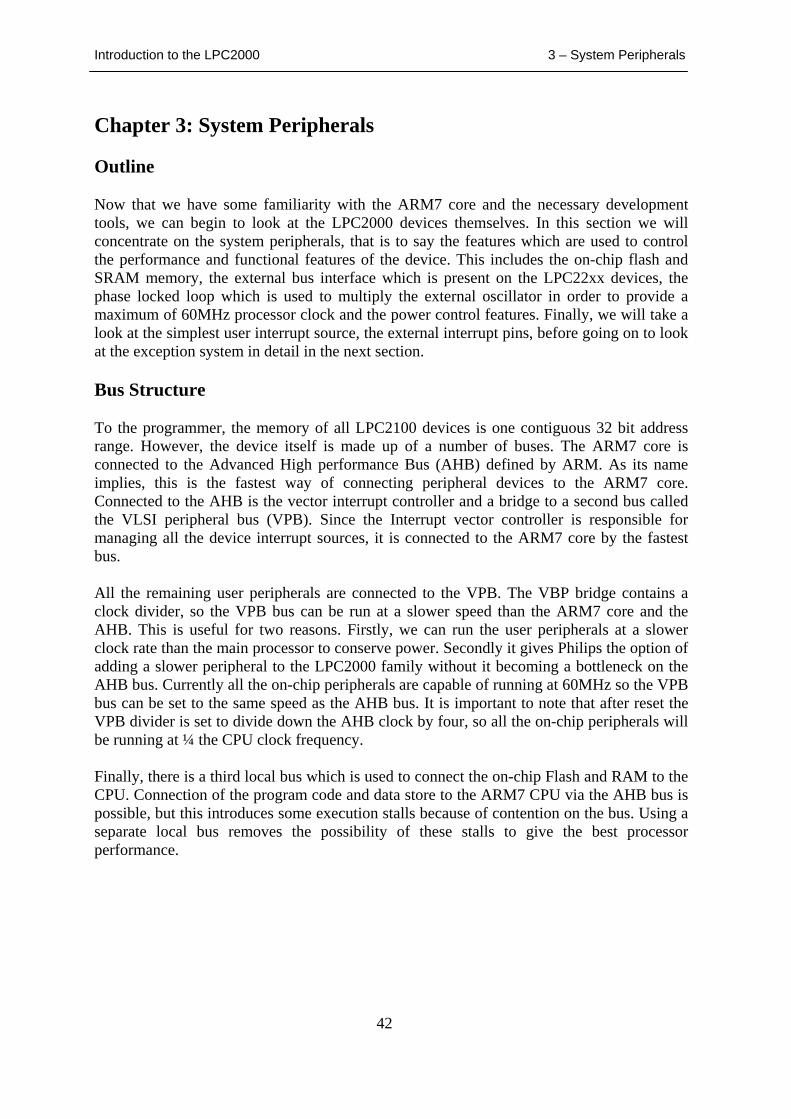
Bus Structure ....................................................................................................................42
Memory Map ....................................................................................................................44
Register Programming.....................................................................................................45
Memory Accelerator Module ..........................................................................................45 Example MAM Configuration .......................................................................................49
FLASH Memory Programming......................................................................................50 Memory Map Control.....................................................................................................50 Bootloader ......................................................................................................................51 Philips ISP Utility...........................................................................................................52 In-Application Programming .........................................................................................53
External Bus Interface .....................................................................................................54 External Memory Interface ............................................................................................54 Using The External Bus Interface ..................................................................................57
Booting From ROM .........................................................................................................58
Phase Locked Loop ..........................................................................................................60
VLSI Peripheral Bus Divider ..........................................................................................62 Example Code: PLL And VPB Configuration........................................................63
Power Control...................................................................................................................64
LPC2000 Interrupt System .............................................................................................66 Pin Connect Block..........................................................................................................66 External Interrupt Pins ...................................................................................................66 Interrupt Structure ..........................................................................................................67 FIQ interrupt...................................................................................................................68 Leaving An FIQ Interrupt ..............................................................................................68
Example Program: FIQ Interrupt ..............................................................................69 Vectored IRQ .................................................................................................................70 Leaving An IRQ Interrupt ..............................................................................................71 Leaving An IRQ Interrupt ..............................................................................................72
Example Program: IRQ interrupt ...............................................................................72 Non-Vectored Interrupts ................................................................................................73 Leaving A Non-Vectored IRQ Interrupt ........................................................................73
Example Program: Non-Vectored Interrupt...............................................................73 Nested Interrupts ............................................................................................................75
Summary...........................................................................................................................76
Chapter 4: User Peripherals........................................................................... 78
Outline ...............................................................................................................................78
Introduction to the LPC2000 Introduction
6
General Purpose I/O ........................................................................................................78
General Purpose Timers..................................................................................................79
PWM Modulator ..............................................................................................................82
Real Time Clock ...............................................................................................................85
Watchdog ..........................................................................................................................88
UART.................................................................................................................................90
I2C Interface.....................................................................................................................94
SPI Interface .....................................................................................................................99
Analog To Digital Converter.........................................................................................101
Digital To Analog Converter.........................................................................................104
CAN Controller ..............................................................................................................105 ISO 7 Layer Model...................................................................................................105
CAN Node Design .......................................................................................................106 CAN Message Objects .................................................................................................107 CAN Bus Arbitration ...................................................................................................109 Bit Timing ....................................................................................................................110 CAN Message Transmission........................................................................................112 CAN Error Containment ..............................................................................................115 CAN Message Reception .............................................................................................118 Acceptance Filtering ....................................................................................................119
Configuring The Acceptance Filter..........................................................................120
Summary.........................................................................................................................122
Chapter 5: Keil Tutorial ............................................................................... 124
Installation ......................................................................................................................124 Using the Keil UVISION IDE .....................................................................................125
Exercise 1: Using the Keil Toolset...................................................................126
Using The Debugger.......................................................................................................133
Using The ULINK Hardware Debugger ......................................................................138 Setting up the ULINK JTAG hardware debugger:.......................................................138
Exercise 2: Startup code...................................................................................141 Exercise 3: Using THUMB code .....................................................................142 Exercise 4: Using STDIO libraries..................................................................144 Exercise 5: Simple interrupt.............................................................................146 Exercise 6: Software Interrupt..........................................................................148 Exercise 7: Memory Accelerator Module ........................................................149 Exercise 8: In-Application programming.........................................................152 Exercise 9: External Bus Interface ...................................................................153 Exercise 10 Phase Locked Loop ......................................................................157 Exercise 11: Fast Interrupt ...............................................................................159 Exercise 12: Vectored Interrupt .......................................................................160 Exercise 13 : Non Vectored Interrupt ..............................................................162 Exercise 14: Nested Interrupts ........................................................................163
Introduction to the LPC2000 Introduction
7
Exercise 15: General purpose IO pins..............................................................164 Exercise 16: Timer Capture..............................................................................165 Exercise 17: Timer Match ................................................................................167 Exercise 18: Dual-Edge (Symmetrical) PWM Generation. .............................170 Exercise 19: Real Time Clock..........................................................................172 Exercise 20: UART ..........................................................................................173 Exercise 21: I2C interface ................................................................................174 Exercise 22: SPI ...............................................................................................175 Exercise 22: SPI ...............................................................................................176 Exercise 23: Analog To Digital Converter.......................................................177 Exercise 24: Digital to Analogue Converter ...................................................178 Exercise 25: Transmitting CAN Data ..............................................................179 Exercise 26: Receiving CAN Data...................................................................180
Chapter 6: Tutorial With GNU Tools ......................................................... 182
Intoduction......................................................................................................................182
GCC Startup Code .........................................................................................................182
Interworking ARM/THUMB Code ..............................................................................182
Accessing Peripherals ....................................................................................................182
Interrupt Service Routines ............................................................................................182 Software Interrupt ........................................................................................................183
Inline Functions ..............................................................................................................183 Exercise 1: Using The Keil Toolset With The GNU Compiler .......................184 Exercise 2: Startup Code ..................................................................................189 Exercise 3: Using THUMB Code.....................................................................190 Exercise 4: Using The GNU Libraries .............................................................192 Exercise 5: Simple Interrupt.............................................................................193 Exercise 6: Software Interrupt..........................................................................195
Appendices ..................................................................................................... 197
Appendix A .....................................................................................................................197 Bibliography.................................................................................................................197 Webliography ...............................................................................................................197
Reference Sites.........................................................................................................197 Tools and Software Development ................................................................................197
Evaluation Boards And Modules ..................................................................................197
Introduction to the LPC2000 Introduction
8
Introduction This book is intended as a hands-on guide for anyone planning to use the Philips LPC2000 family of microcontrollers in a new design. It is laid out both as a reference book and as a tutorial. It is assumed that you have some experience in programming microcontrollers for embedded systems and are familiar with the C language. The bulk of technical information is spread over the first four chapters, which should be read in order if you are completely new to the LPC2000 and the ARM7 CPU. The first chapter gives an introduction to the major features of the ARM7 CPU. Reading this chapter will give you enough understanding to be able to program any ARM7 device. If you want to develop your knowledge further, there are a number of excellent books which describe this architecture and some of these are listed in the bibliography. Chapter Two is a description of how to write C programs to run on an ARM7 processor and, as such, describes specific extensions to the ISO C standard which are necessary for embedded programming. In this book a commercial compiler is used in the main text, however the GCC tools have also been ported to ARM. Appendix A details the ARM-specific features of the GCC tools. Having read the first two chapters you should understand the processor and its development tools. Chapter Three then introduces the LPC2000 system peripherals. This chapter describes the system architecture of the LPC2000 family and how to set the chip up for its best performance. In Chapter Four we look at the on-chip user peripherals and how to configure them for our application code. Throughout these chapters various exercises are listed. Each of these exercises are described in detail in Chapter Five, the Tutorial section. The Tutorial contains a worksheet for each exercise which steps you through an important aspect of the LPC200. All of the exercises can be done with the evaluation compiler and simulator which come on the CD provided with this book. A low-cost starter kit is also available which allows you to download the example code on to some real hardware and “prove” that it does in fact work. It is hoped that by reading the book and doing the exercises you will quickly become familiar with the LPC2000.

Introduction to the LPC2000 Introduction
9
Introduction to the LPC2000 1 - The ARM7 CPU Core
10
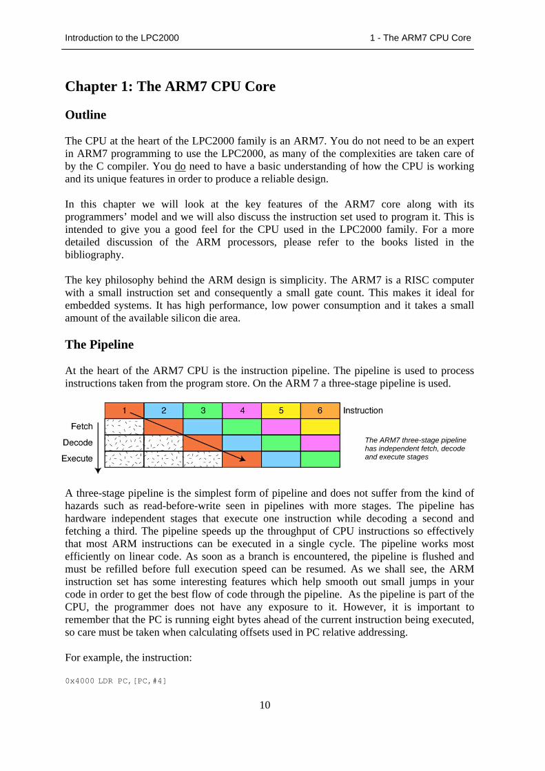
Chapter 1: The ARM7 CPU Core Outline The CPU at the heart of the LPC2000 family is an ARM7. You do not need to be an expert in ARM7 programming to use the LPC2000, as many of the complexities are taken care of by the C compiler. You do need to have a basic understanding of how the CPU is working and its unique features in order to produce a reliable design. In this chapter we will look at the key features of the ARM7 core along with its programmers’ model and we will also discuss the instruction set used to program it. This is intended to give you a good feel for the CPU used in the LPC2000 family. For a more detailed discussion of the ARM processors, please refer to the books listed in the bibliography. The key philosophy behind the ARM design is simplicity. The ARM7 is a RISC computer with a small instruction set and consequently a small gate count. This makes it ideal for embedded systems. It has high performance, low power consumption and it takes a small amount of the available silicon die area. The Pipeline At the heart of the ARM7 CPU is the instruction pipeline. The pipeline is used to process instructions taken from the program store. On the ARM 7 a three-stage pipeline is used.
A three-stage pipeline is the simplest form of pipeline and does not suffer from the kind of hazards such as read-before-write seen in pipelines with more stages. The pipeline has hardware independent stages that execute one instruction while decoding a second and fetching a third. The pipeline speeds up the throughput of CPU instructions so effectively that most ARM instructions can be executed in a single cycle. The pipeline works most efficiently on linear code. As soon as a branch is encountered, the pipeline is flushed and must be refilled before full execution speed can be resumed. As we shall see, the ARM instruction set has some interesting features which help smooth out small jumps in your code in order to get the best flow of code through the pipeline. As the pipeline is part of the CPU, the programmer does not have any exposure to it. However, it is important to remember that the PC is running eight bytes ahead of the current instruction being executed, so care must be taken when calculating offsets used in PC relative addressing. For example, the instruction: 0x4000 LDR PC,[PC,#4]
The ARM7 three-stage pipeline has independent fetch, decode and execute stages
Introduction to the LPC2000 1 - The ARM7 CPU Core
11
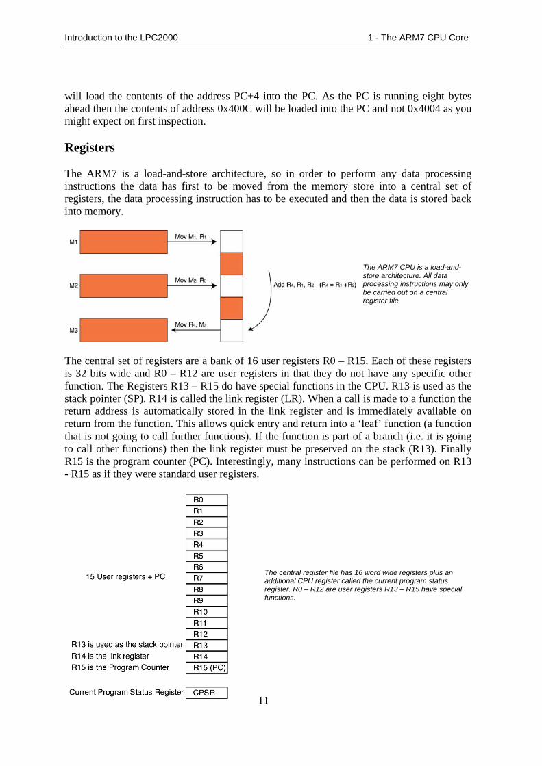
will load the contents of the address PC+4 into the PC. As the PC is running eight bytes ahead then the contents of address 0x400C will be loaded into the PC and not 0x4004 as you might expect on first inspection. Registers The ARM7 is a load-and-store architecture, so in order to perform any data processing instructions the data has first to be moved from the memory store into a central set of registers, the data processing instruction has to be executed and then the data is stored back into memory.
The central set of registers are a bank of 16 user registers R0 – R15. Each of these registers is 32 bits wide and R0 – R12 are user registers in that they do not have any specific other function. The Registers R13 – R15 do have special functions in the CPU. R13 is used as the stack pointer (SP). R14 is called the link register (LR). When a call is made to a function the return address is automatically stored in the link register and is immediately available on return from the function. This allows quick entry and return into a ‘leaf’ function (a function that is not going to call further functions). If the function is part of a branch (i.e. it is going to call other functions) then the link register must be preserved on the stack (R13). Finally R15 is the program counter (PC). Interestingly, many instructions can be performed on R13 - R15 as if they were standard user registers.
The ARM7 CPU is a load-and-store architecture. All data processing instructions may only be carried out on a central register file
The central register file has 16 word wide registers plus an additional CPU register called the current program status register. R0 – R12 are user registers R13 – R15 have special functions.
Introduction to the LPC2000 1 - The ARM7 CPU Core
12
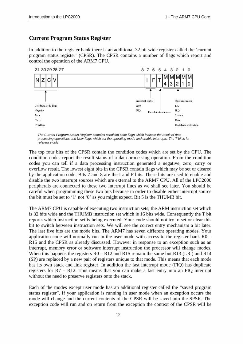
Current Program Status Register In addition to the register bank there is an additional 32 bit wide register called the ‘current program status register’ (CPSR). The CPSR contains a number of flags which report and control the operation of the ARM7 CPU.
The top four bits of the CPSR contain the condition codes which are set by the CPU. The condition codes report the result status of a data processing operation. From the condition codes you can tell if a data processing instruction generated a negative, zero, carry or overflow result. The lowest eight bits in the CPSR contain flags which may be set or cleared by the application code. Bits 7 and 8 are the I and F bits. These bits are used to enable and disable the two interrupt sources which are external to the ARM7 CPU. All of the LPC2000 peripherals are connected to these two interrupt lines as we shall see later. You should be careful when programming these two bits because in order to disable either interrupt source the bit must be set to ‘1’ not ‘0’ as you might expect. Bit 5 is the THUMB bit. The ARM7 CPU is capable of executing two instruction sets; the ARM instruction set which is 32 bits wide and the THUMB instruction set which is 16 bits wide. Consequently the T bit reports which instruction set is being executed. Your code should not try to set or clear this bit to switch between instruction sets. We will see the correct entry mechanism a bit later. The last five bits are the mode bits. The ARM7 has seven different operating modes. Your application code will normally run in the user mode with access to the register bank R0 – R15 and the CPSR as already discussed. However in response to an exception such as an interrupt, memory error or software interrupt instruction the processor will change modes. When this happens the registers R0 – R12 and R15 remain the same but R13 (LR ) and R14 (SP) are replaced by a new pair of registers unique to that mode. This means that each mode has its own stack and link register. In addition the fast interrupt mode (FIQ) has duplicate registers for R7 – R12. This means that you can make a fast entry into an FIQ interrupt without the need to preserve registers onto the stack. Each of the modes except user mode has an additional register called the “saved program status register”. If your application is running in user mode when an exception occurs the mode will change and the current contents of the CPSR will be saved into the SPSR. The exception code will run and on return from the exception the context of the CPSR will be
The Current Program Status Register contains condition code flags which indicate the result of data processing operations and User flags which set the operating mode and enable interrupts. The T bit is for reference only
Introduction to the LPC2000 1 - The ARM7 CPU Core
13
restored from the SPSR allowing the application code to resume execution. The operating modes are listed below.
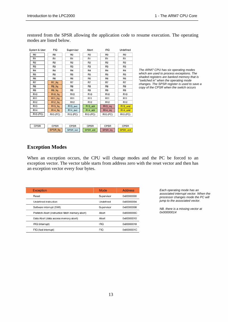
Exception Modes When an exception occurs, the CPU will change modes and the PC be forced to an exception vector. The vector table starts from address zero with the reset vector and then has an exception vector every four bytes.
The ARM7 CPU has six operating modes which are used to process exceptions. The shaded registers are banked memory that is “switched in” when the operating mode changes. The SPSR register is used to save a copy of the CPSR when the switch occurs
Each operating mode has an associated interrupt vector. When the processor changes mode the PC will jump to the associated vector.
NB. there is a missing vector at 0x00000014
Introduction to the LPC2000 1 - The ARM7 CPU Core
14
NB: There is a gap in the vector table because there is a missing vector at 0x00000014. This location was used on an earlier ARM architecture and has been preserved on ARM7 to ensure software compatibility between different ARM architectures. However in the LPC2000 family these four bytes are used for a very special purpose as we shall see later.
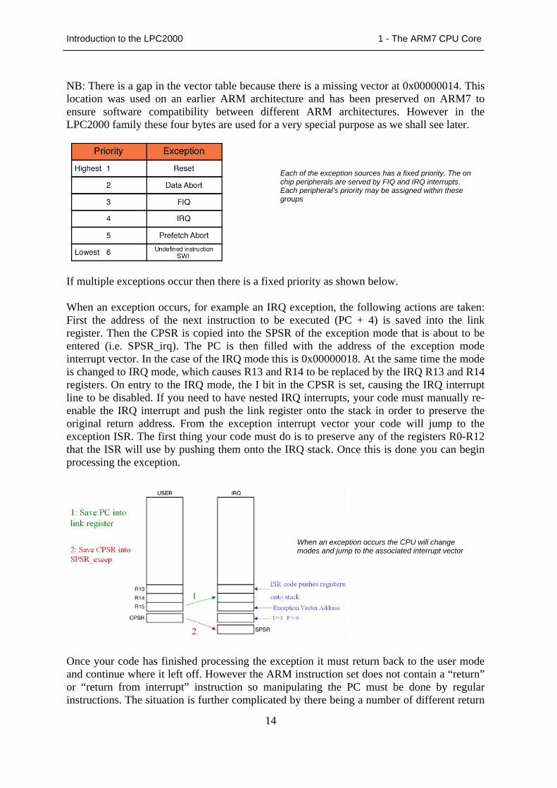
If multiple exceptions occur then there is a fixed priority as shown below. When an exception occurs, for example an IRQ exception, the following actions are taken: First the address of the next instruction to be executed (PC + 4) is saved into the link register. Then the CPSR is copied into the SPSR of the exception mode that is about to be entered (i.e. SPSR_irq). The PC is then filled with the address of the exception mode interrupt vector. In the case of the IRQ mode this is 0x00000018. At the same time the mode is changed to IRQ mode, which causes R13 and R14 to be replaced by the IRQ R13 and R14 registers. On entry to the IRQ mode, the I bit in the CPSR is set, causing the IRQ interrupt line to be disabled. If you need to have nested IRQ interrupts, your code must manually re-enable the IRQ interrupt and push the link register onto the stack in order to preserve the original return address. From the exception interrupt vector your code will jump to the exception ISR. The first thing your code must do is to preserve any of the registers R0-R12 that the ISR will use by pushing them onto the IRQ stack. Once this is done you can begin processing the exception.
Once your code has finished processing the exception it must return back to the user mode and continue where it left off. However the ARM instruction set does not contain a “return” or “return from interrupt” instruction so manipulating the PC must be done by regular instructions. The situation is further complicated by there being a number of different return
Each of the exception sources has a fixed priority. The on chip peripherals are served by FIQ and IRQ interrupts. Each peripheral’s priority may be assigned within these groups
When an exception occurs the CPU will change modes and jump to the associated interrupt vector
Introduction to the LPC2000 1 - The ARM7 CPU Core
15
cases. First of all, consider the SWI instruction. In this case the SWI instruction is executed, the address of the next instruction to be executed is stored in the Link register and the exception is processed. In order to return from the exception all that is necessary is to move the contents of the link register into the PC and processing can continue. However in order to make the CPU switch modes back to user mode, a modified version of the move instruction is used and this is called MOVS (more about this later). Hence for a software interrupt the return instruction is MOVS R15,R14 ; Move Link register into the PC and switch modes.
However, in the case of the FIQ and IRQ instructions, when an exception occurs the current instruction being executed is discarded and the exception is entered. When the code returns from the exception the link register contains the address of the discarded instruction plus four. In order to resume processing at the correct point we need to roll back the value in the Link register by four. In this case we use the subtract instruction to deduct four from the link register and store the results in the PC. As with the move instruction, there is a form of the subtract instruction which will also restore the operating mode. For an IRQ, FIQ or Prog Abort, the return instruction is: SUBS R15, R14,#4
In the case of a data abort instruction, the exception will occur one instruction after execution of the instruction which caused the exception. In this case we will ideally enter the data abort ISR, sort out the problem with the memory and return to reprocess the instruction that caused the exception. In this case we have to roll back the PC by two instructions i.e. the discarded instruction and the instruction that caused the exception. In other words subtract eight from the link register and store the result in the PC. For a data abort exception the return instruction is SUBS R15, R14,#8
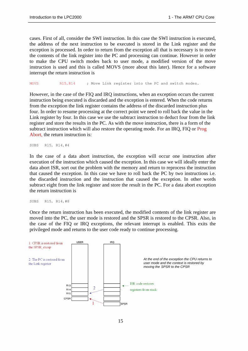
Once the return instruction has been executed, the modified contents of the link register are moved into the PC, the user mode is restored and the SPSR is restored to the CPSR. Also, in the case of the FIQ or IRQ exceptions, the relevant interrupt is enabled. This exits the privileged mode and returns to the user code ready to continue processing.
At the end of the exception the CPU returns to user mode and the context is restored by moving the SPSR to the CPSR
Introduction to the LPC2000 1 - The ARM7 CPU Core
16
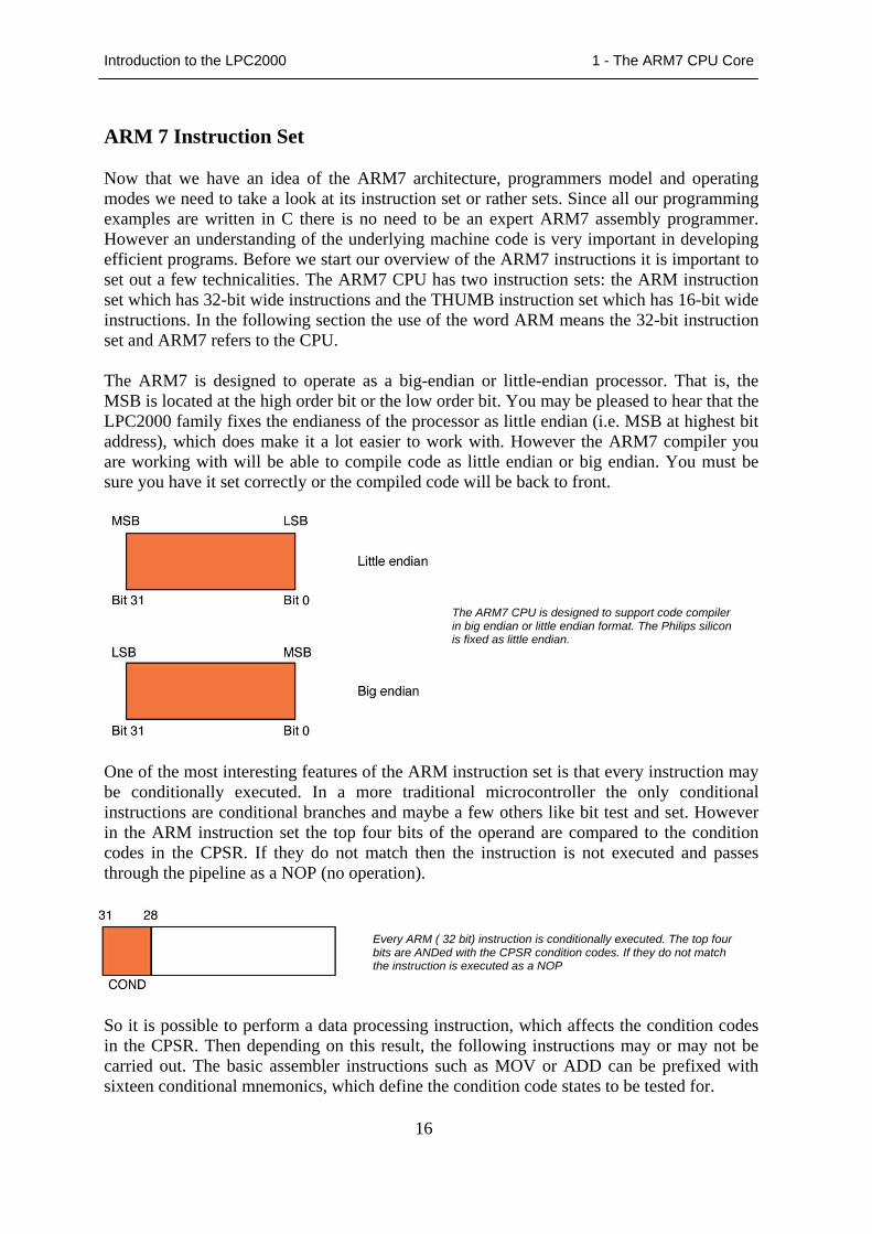
ARM 7 Instruction Set Now that we have an idea of the ARM7 architecture, programmers model and operating modes we need to take a look at its instruction set or rather sets. Since all our programming examples are written in C there is no need to be an expert ARM7 assembly programmer. However an understanding of the underlying machine code is very important in developing efficient programs. Before we start our overview of the ARM7 instructions it is important to set out a few technicalities. The ARM7 CPU has two instruction sets: the ARM instruction set which has 32-bit wide instructions and the THUMB instruction set which has 16-bit wide instructions. In the following section the use of the word ARM means the 32-bit instruction set and ARM7 refers to the CPU. The ARM7 is designed to operate as a big-endian or little-endian processor. That is, the MSB is located at the high order bit or the low order bit. You may be pleased to hear that the LPC2000 family fixes the endianess of the processor as little endian (i.e. MSB at highest bit address), which does make it a lot easier to work with. However the ARM7 compiler you are working with will be able to compile code as little endian or big endian. You must be sure you have it set correctly or the compiled code will be back to front.
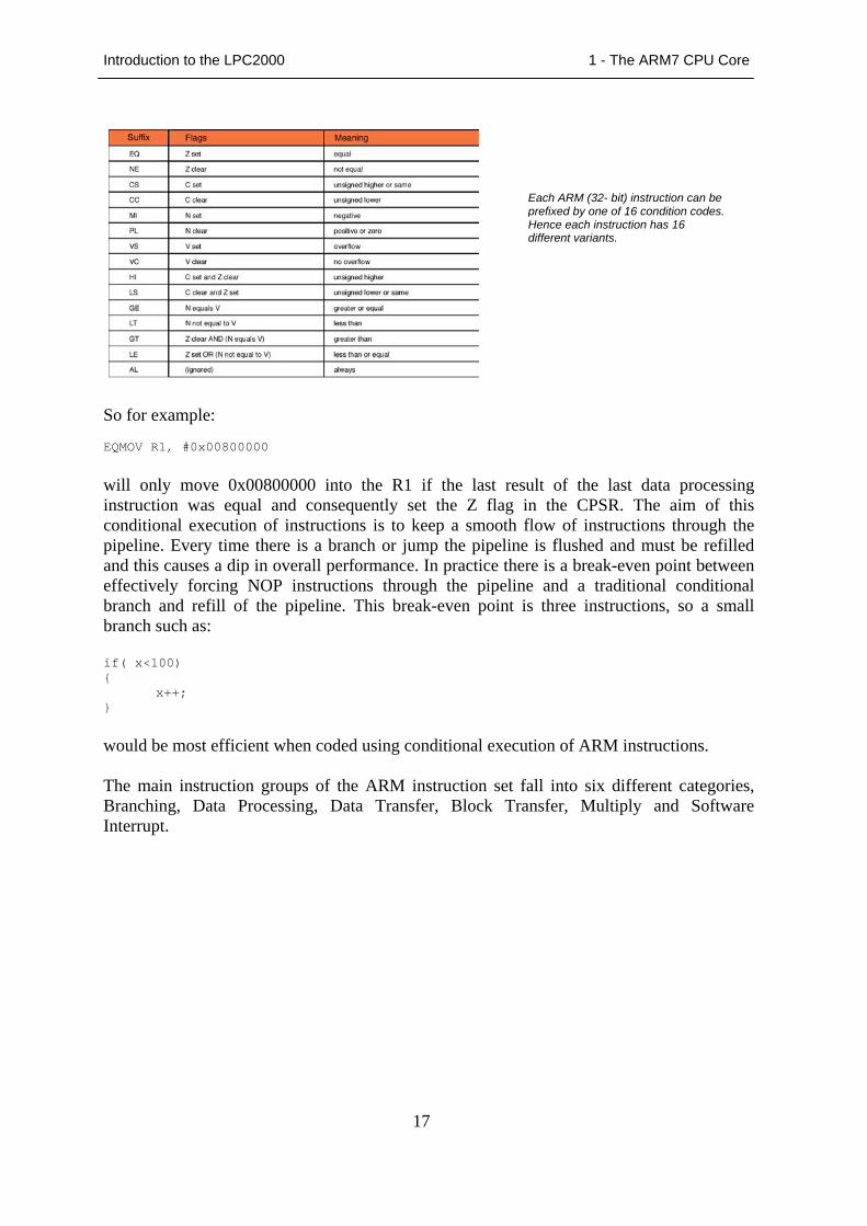
One of the most interesting features of the ARM instruction set is that every instruction may be conditionally executed. In a more traditional microcontroller the only conditional instructions are conditional branches and maybe a few others like bit test and set. However in the ARM instruction set the top four bits of the operand are compared to the condition codes in the CPSR. If they do not match then the instruction is not executed and passes through the pipeline as a NOP (no operation).
So it is possible to perform a data processing instruction, which affects the condition codes in the CPSR. Then depending on this result, the following instructions may or may not be carried out. The basic assembler instructions such as MOV or ADD can be prefixed with sixteen conditional mnemonics, which define the condition code states to be tested for.
The ARM7 CPU is designed to support code compiler in big endian or little endian format. The Philips silicon is fixed as little endian.
Every ARM ( 32 bit) instruction is conditionally executed. The top four bits are ANDed with the CPSR condition codes. If they do not match the instruction is executed as a NOP
Introduction to the LPC2000 1 - The ARM7 CPU Core
17
So for example: EQMOV R1, #0x00800000
will only move 0x00800000 into the R1 if the last result of the last data processing instruction was equal and consequently set the Z flag in the CPSR. The aim of this conditional execution of instructions is to keep a smooth flow of instructions through the pipeline. Every time there is a branch or jump the pipeline is flushed and must be refilled and this causes a dip in overall performance. In practice there is a break-even point between effectively forcing NOP instructions through the pipeline and a traditional conditional branch and refill of the pipeline. This break-even point is three instructions, so a small branch such as: if( x<100) { x++; }
would be most efficient when coded using conditional execution of ARM instructions. The main instruction groups of the ARM instruction set fall into six different categories, Branching, Data Processing, Data Transfer, Block Transfer, Multiply and Software Interrupt.
Each ARM (32- bit) instruction can be prefixed by one of 16 condition codes. Hence each instruction has 16 different variants.
Introduction to the LPC2000 1 - The ARM7 CPU Core
18
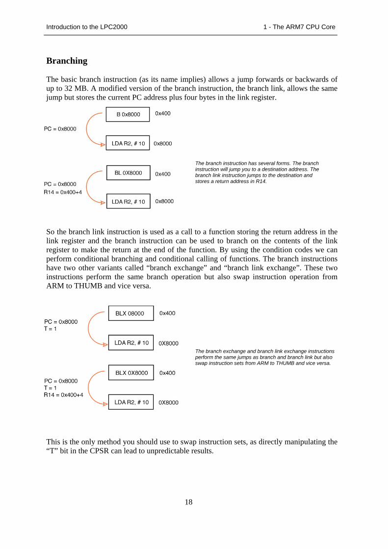
Branching The basic branch instruction (as its name implies) allows a jump forwards or backwards of up to 32 MB. A modified version of the branch instruction, the branch link, allows the same jump but stores the current PC address plus four bytes in the link register.
So the branch link instruction is used as a call to a function storing the return address in the link register and the branch instruction can be used to branch on the contents of the link register to make the return at the end of the function. By using the condition codes we can perform conditional branching and conditional calling of functions. The branch instructions have two other variants called “branch exchange” and “branch link exchange”. These two instructions perform the same branch operation but also swap instruction operation from ARM to THUMB and vice versa.
This is the only method you should use to swap instruction sets, as directly manipulating the “T” bit in the CPSR can lead to unpredictable results.
The branch instruction has several forms. The branch instruction will jump you to a destination address. The branch link instruction jumps to the destination and stores a return address in R14.
The branch exchange and branch link exchange instructions perform the same jumps as branch and branch link but also swap instruction sets from ARM to THUMB and vice versa.
Introduction to the LPC2000 1 - The ARM7 CPU Core
19
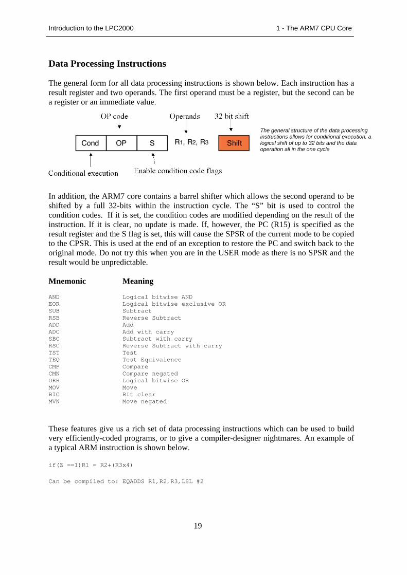
Data Processing Instructions The general form for all data processing instructions is shown below. Each instruction has a result register and two operands. The first operand must be a register, but the second can be a register or an immediate value.
In addition, the ARM7 core contains a barrel shifter which allows the second operand to be shifted by a full 32-bits within the instruction cycle. The “S” bit is used to control the condition codes. If it is set, the condition codes are modified depending on the result of the instruction. If it is clear, no update is made. If, however, the PC (R15) is specified as the result register and the S flag is set, this will cause the SPSR of the current mode to be copied to the CPSR. This is used at the end of an exception to restore the PC and switch back to the original mode. Do not try this when you are in the USER mode as there is no SPSR and the result would be unpredictable. Mnemonic Meaning AND Logical bitwise AND EOR Logical bitwise exclusive OR SUB Subtract RSB Reverse Subtract ADD Add ADC Add with carry SBC Subtract with carry RSC Reverse Subtract with carry TST Test TEQ Test Equivalence CMP Compare CMN Compare negated ORR Logical bitwise OR MOV Move BIC Bit clear MVN Move negated
These features give us a rich set of data processing instructions which can be used to build very efficiently-coded programs, or to give a compiler-designer nightmares. An example of a typical ARM instruction is shown below. if(Z ==1)R1 = R2+(R3x4)
Can be compiled to: EQADDS R1,R2,R3,LSL #2
The general structure of the data processing instructions allows for conditional execution, a logical shift of up to 32 bits and the data operation all in the one cycle
Introduction to the LPC2000 1 - The ARM7 CPU Core
20
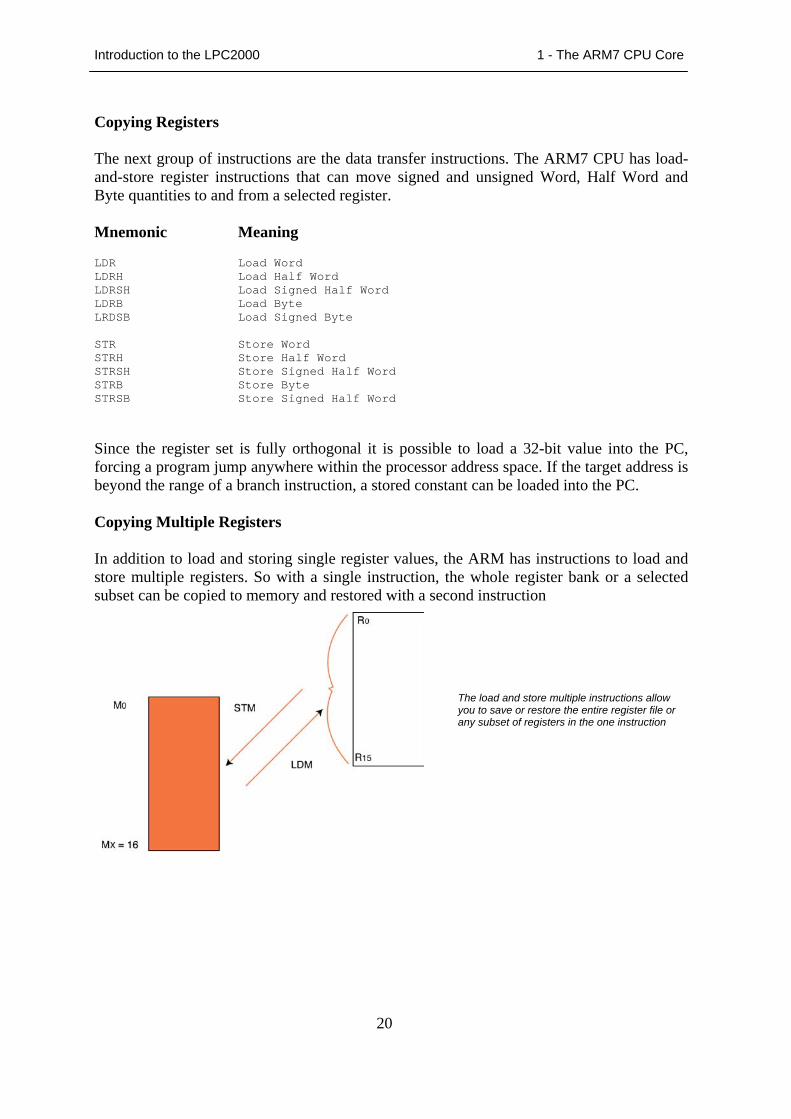
Copying Registers The next group of instructions are the data transfer instructions. The ARM7 CPU has load-and-store register instructions that can move signed and unsigned Word, Half Word and Byte quantities to and from a selected register. Mnemonic Meaning LDR Load Word LDRH Load Half Word LDRSH Load Signed Half Word LDRB Load Byte LRDSB Load Signed Byte STR Store Word STRH Store Half Word STRSH Store Signed Half Word STRB Store Byte STRSB Store Signed Half Word Since the register set is fully orthogonal it is possible to load a 32-bit value into the PC, forcing a program jump anywhere within the processor address space. If the target address is beyond the range of a branch instruction, a stored constant can be loaded into the PC. Copying Multiple Registers In addition to load and storing single register values, the ARM has instructions to load and store multiple registers. So with a single instruction, the whole register bank or a selected subset can be copied to memory and restored with a second instruction
The load and store multiple instructions allow you to save or restore the entire register file or any subset of registers in the one instruction
Introduction to the LPC2000 1 - The ARM7 CPU Core
21
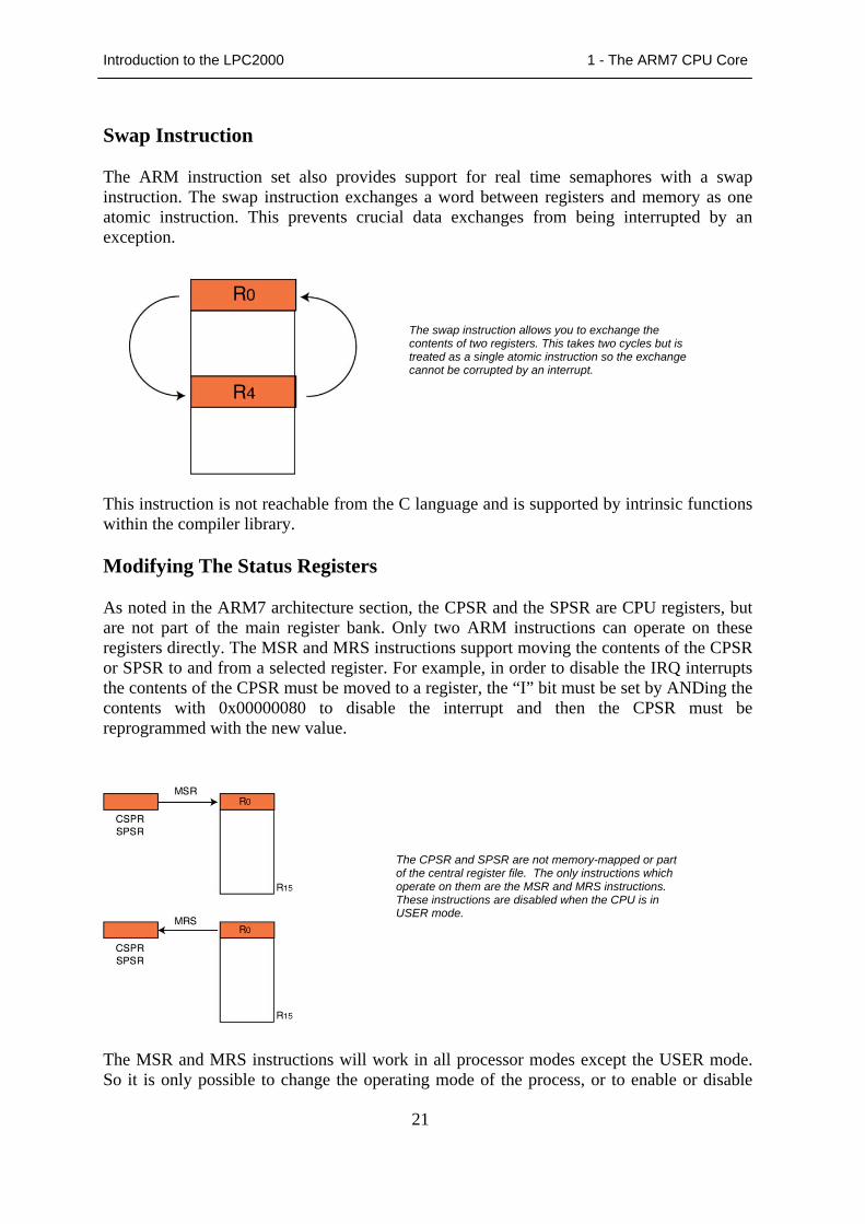
Swap Instruction The ARM instruction set also provides support for real time semaphores with a swap instruction. The swap instruction exchanges a word between registers and memory as one atomic instruction. This prevents crucial data exchanges from being interrupted by an exception.
This instruction is not reachable from the C language and is supported by intrinsic functions within the compiler library. Modifying The Status Registers As noted in the ARM7 architecture section, the CPSR and the SPSR are CPU registers, but are not part of the main register bank. Only two ARM instructions can operate on these registers directly. The MSR and MRS instructions support moving the contents of the CPSR or SPSR to and from a selected register. For example, in order to disable the IRQ interrupts the contents of the CPSR must be moved to a register, the “I” bit must be set by ANDing the contents with 0x00000080 to disable the interrupt and then the CPSR must be reprogrammed with the new value.
The MSR and MRS instructions will work in all processor modes except the USER mode. So it is only possible to change the operating mode of the process, or to enable or disable
The swap instruction allows you to exchange the contents of two registers. This takes two cycles but is treated as a single atomic instruction so the exchange cannot be corrupted by an interrupt.
The CPSR and SPSR are not memory-mapped or part of the central register file. The only instructions which operate on them are the MSR and MRS instructions. These instructions are disabled when the CPU is in USER mode.
Introduction to the LPC2000 1 - The ARM7 CPU Core
22
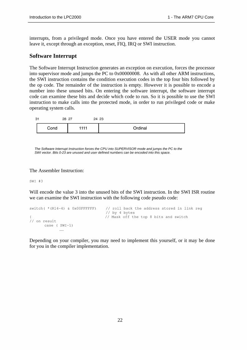
interrupts, from a privileged mode. Once you have entered the USER mode you cannot leave it, except through an exception, reset, FIQ, IRQ or SWI instruction. Software Interrupt The Software Interrupt Instruction generates an exception on execution, forces the processor into supervisor mode and jumps the PC to 0x00000008. As with all other ARM instructions, the SWI instruction contains the condition execution codes in the top four bits followed by the op code. The remainder of the instruction is empty. However it is possible to encode a number into these unused bits. On entering the software interrupt, the software interrupt code can examine these bits and decide which code to run. So it is possible to use the SWI instruction to make calls into the protected mode, in order to run privileged code or make operating system calls.
The Assembler Instruction: SWI #3
Will encode the value 3 into the unused bits of the SWI instruction. In the SWI ISR routine we can examine the SWI instruction with the following code pseudo code: switch( *(R14-4) & 0x00FFFFFF) // roll back the address stored in link reg // by 4 bytes { // Mask off the top 8 bits and switch // on result case ( SWI-1) ……
Depending on your compiler, you may need to implement this yourself, or it may be done for you in the compiler implementation.
The Software Interrupt Instruction forces the CPU into SUPERVISOR mode and jumps the PC to the SWI vector. Bits 0-23 are unused and user defined numbers can be encoded into this space.
Introduction to the LPC2000 1 - The ARM7 CPU Core
23
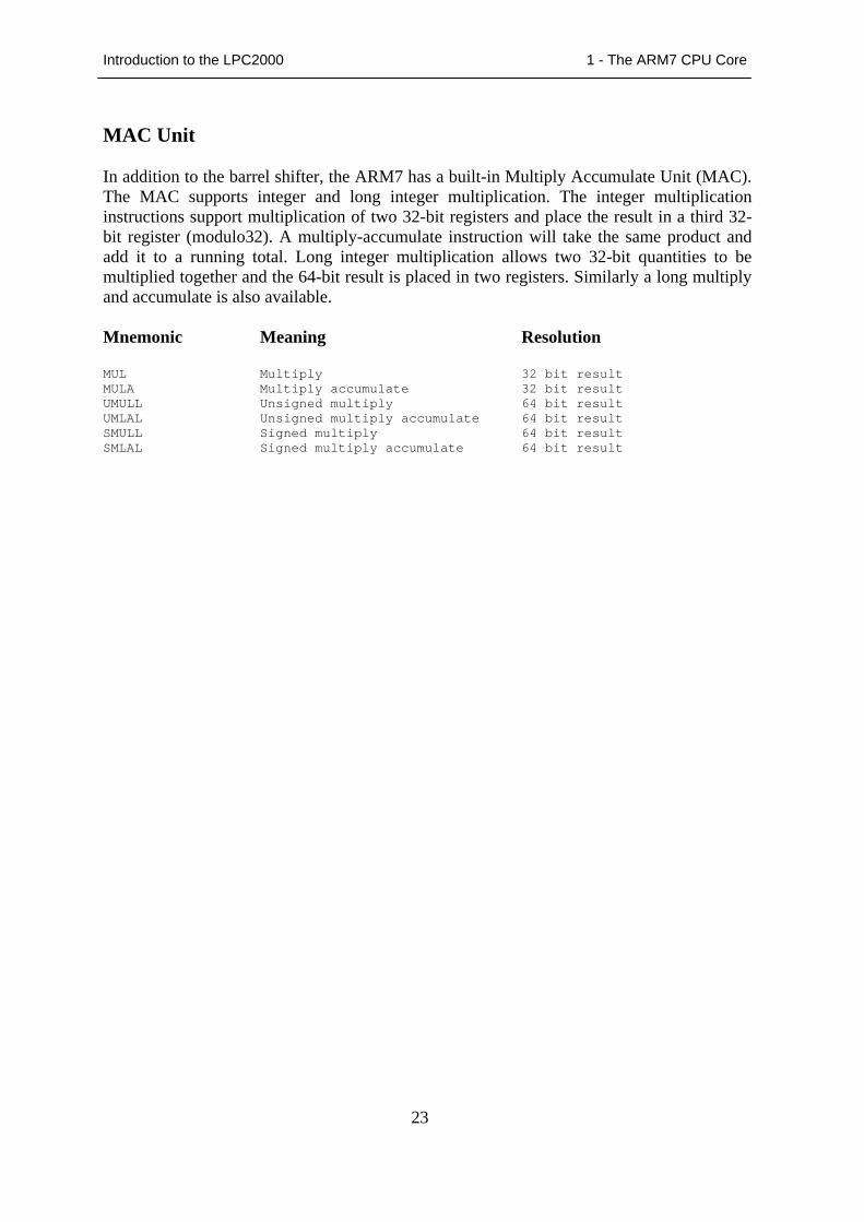
MAC Unit In addition to the barrel shifter, the ARM7 has a built-in Multiply Accumulate Unit (MAC). The MAC supports integer and long integer multiplication. The integer multiplication instructions support multiplication of two 32-bit registers and place the result in a third 32-bit register (modulo32). A multiply-accumulate instruction will take the same product and add it to a running total. Long integer multiplication allows two 32-bit quantities to be multiplied together and the 64-bit result is placed in two registers. Similarly a long multiply and accumulate is also available. Mnemonic Meaning Resolution MUL Multiply 32 bit result MULA Multiply accumulate 32 bit result UMULL Unsigned multiply 64 bit result UMLAL Unsigned multiply accumulate 64 bit result SMULL Signed multiply 64 bit result SMLAL Signed multiply accumulate 64 bit result
Introduction to the LPC2000 1 - The ARM7 CPU Core
24
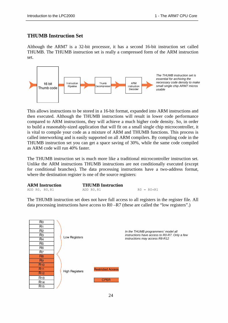
THUMB Instruction Set Although the ARM7 is a 32-bit processor, it has a second 16-bit instruction set called THUMB. The THUMB instruction set is really a compressed form of the ARM instruction set.
This allows instructions to be stored in a 16-bit format, expanded into ARM instructions and then executed. Although the THUMB instructions will result in lower code performance compared to ARM instructions, they will achieve a much higher code density. So, in order to build a reasonably-sized application that will fit on a small single chip microcontroller, it is vital to compile your code as a mixture of ARM and THUMB functions. This process is called interworking and is easily supported on all ARM compilers. By compiling code in the THUMB instruction set you can get a space saving of 30%, while the same code compiled as ARM code will run 40% faster. The THUMB instruction set is much more like a traditional microcontroller instruction set. Unlike the ARM instructions THUMB instructions are not conditionally executed (except for conditional branches). The data processing instructions have a two-address format, where the destination register is one of the source registers: ARM Instruction THUMB Instruction ADD R0, R0,R1 ADD R0,R1 R0 = R0+R1
The THUMB instruction set does not have full access to all registers in the register file. All data processing instructions have access to R0 –R7 (these are called the “low registers”.)
The THUMB instruction set is essential for archiving the necessary code density to make small single chip ARM7 micros usable
In the THUMB programmers’ model all instructions have access to R0-R7. Only a few instructions may access R8-R12
Introduction to the LPC2000 1 - The ARM7 CPU Core
25
However access to R8-R12 (the “high registers”) is restricted to a few instructions: MOV, ADD, CMP
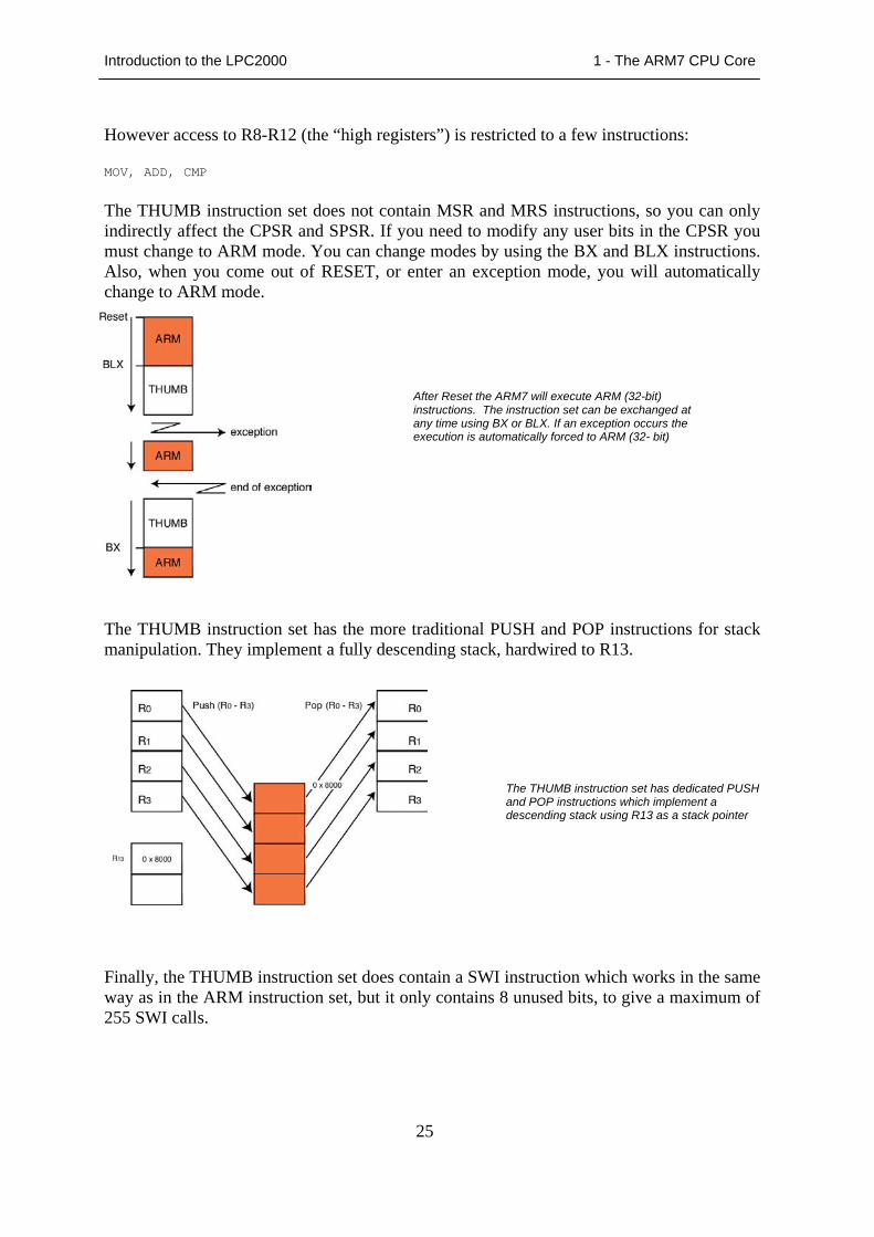
The THUMB instruction set does not contain MSR and MRS instructions, so you can only indirectly affect the CPSR and SPSR. If you need to modify any user bits in the CPSR you must change to ARM mode. You can change modes by using the BX and BLX instructions. Also, when you come out of RESET, or enter an exception mode, you will automatically change to ARM mode.
The THUMB instruction set has the more traditional PUSH and POP instructions for stack manipulation. They implement a fully descending stack, hardwired to R13.
Finally, the THUMB instruction set does contain a SWI instruction which works in the same way as in the ARM instruction set, but it only contains 8 unused bits, to give a maximum of 255 SWI calls.
After Reset the ARM7 will execute ARM (32-bit) instructions. The instruction set can be exchanged at any time using BX or BLX. If an exception occurs the execution is automatically forced to ARM (32- bit)
The THUMB instruction set has dedicated PUSH and POP instructions which implement a descending stack using R13 as a stack pointer

Introduction to the LPC2000 1 - The ARM7 CPU Core
26
Summary At the end of this chapter you should have a basic understanding of the ARM7 CPU. Please see the bibliography for a list of books that address the ARM7 in more detail. Also included on the CD is a copy of the ARM7 user manual.
Introduction to the LPC2000 2 – Software Development
27
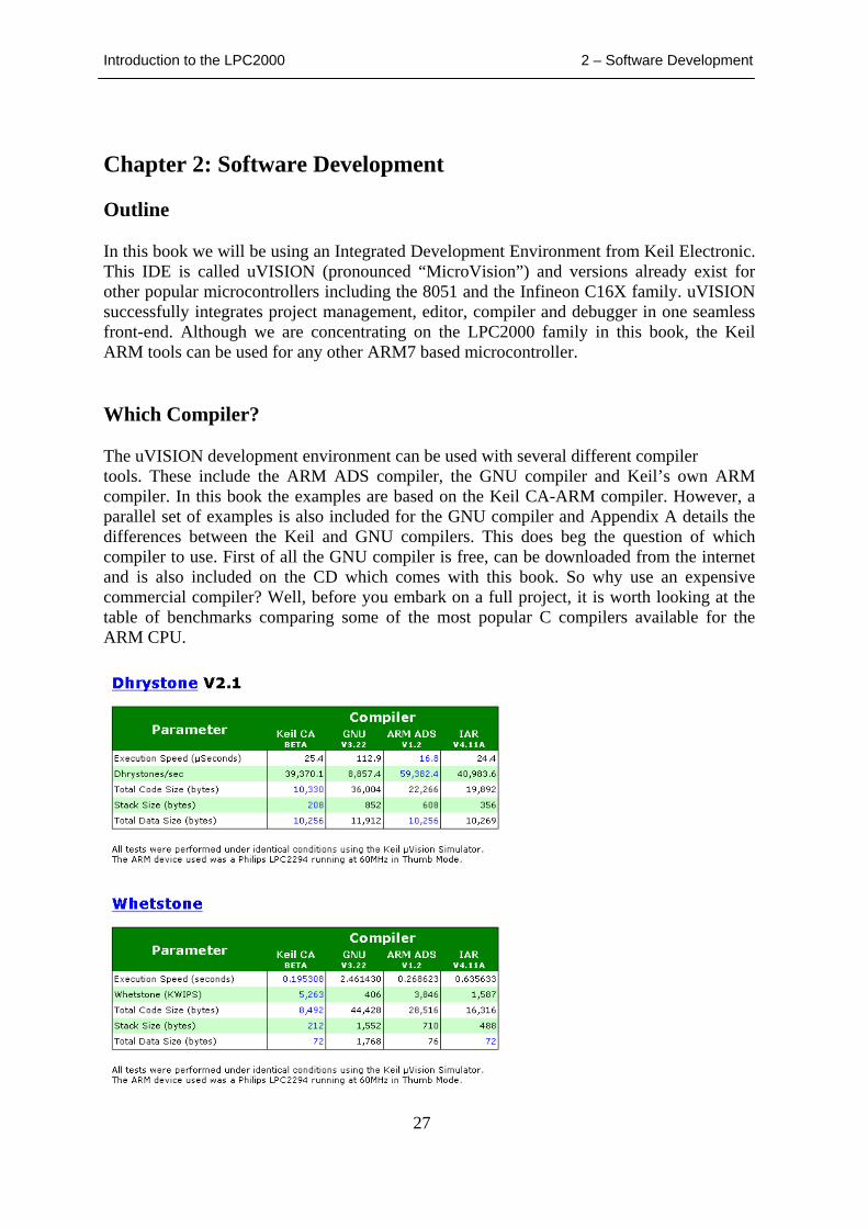
Chapter 2: Software Development Outline In this book we will be using an Integrated Development Environment from Keil Electronic. This IDE is called uVISION (pronounced “MicroVision”) and versions already exist for other popular microcontrollers including the 8051 and the Infineon C16X family. uVISION successfully integrates project management, editor, compiler and debugger in one seamless front-end. Although we are concentrating on the LPC2000 family in this book, the Keil ARM tools can be used for any other ARM7 based microcontroller. Which Compiler? The uVISION development environment can be used with several different compiler tools. These include the ARM ADS compiler, the GNU compiler and Keil’s own ARM compiler. In this book the examples are based on the Keil CA-ARM compiler. However, a parallel set of examples is also included for the GNU compiler and Appendix A details the differences between the Keil and GNU compilers. This does beg the question of which compiler to use. First of all the GNU compiler is free, can be downloaded from the internet and is also included on the CD which comes with this book. So why use an expensive commercial compiler? Well, before you embark on a full project, it is worth looking at the table of benchmarks comparing some of the most popular C compilers available for the ARM CPU.
Introduction to the LPC2000 2 – Software Development
28
We can see from this simple analysis that the commercial compilers are streets ahead of the GNU tools in terms of code density and speed of execution. The reasons to use each of the given compilers can be summed up as follows: if you want the fastest code and standard tools use the ARM compiler, for best code density use the Keil, if you have no budget or a simple project use the GNU. Since we are writing code for a small single-chip microcontroller with limited on-chip resources, the obvious choice for us is the Keil ARM compiler. When deciding on a toolset it is also important to examine how much support is given to a specific ARM7 implementation. Although a toolset may generate code for an ARM7, it may not understand how the ARM7 is being used in a specific system i.e. LPC2000. Using a “raw” ARM7 will generate code, which will run on the LPC2000, but you will have to spend time writing the start-up code and struggle with a debugger, which will not understand the LPC peripherals. This can lead to “fighting” the development tools, which needless to say can be very frustrating. uVISION IDE uVISION also includes two debug tools. Once the code has been compiled and linked, it can be loaded into the uVISION simulator. This debugger simulates the ARM7 core and peripherals of the supported micro. Using the simulator is a very good way of becoming familiar with the LPC2000 devices. Since the simulator gives cycle- accurate simulation of the peripherals, as well as the CPU, it can be a very useful tool for verifying that the chip has been correctly initialised and that the correct values for things such as timer prescaler values have been calculated. However, the simulator can only take you so far and sooner or later you will need to take some inputs from the real world. This can be done to a certain extent with the simulator scripting language, but eventually you will need to run your code on the real target. The simulator front end can be connected to your hardware by the Keil ULINK interface. The ULINK interface connects to the PC via USB and connects to the development hardware by the LPC2000 JTAG interface. The JTAG interface is a separate peripheral on the ARM7 which supports debug commands from a host. By using the JTAG you can use the uVISION simulator to have basic run control of the LPC2000 device. The JTAG allows you to download code onto the target, to single step and run code at full speed, to set breakpoints and view memory locations. Tutorial Included with this book is a demonstration version of the Keil uVISION IDE. The installation comes with two compilers, the Keil ARM compiler and the GNU tools. The tutorial section talks you through example programs illustrating the major features of the LPC2000. These examples can be run on the simulator, or if you have the starter kit they can be downloaded and run on the MCB2100 evaluation board. There are two sets of examples on the CD, one for the Keil compiler and one for the GNU. The main text concentrates on the Keil compiler. However, Appendix A describes how to use the GNU compiler and also
Introduction to the LPC2000 2 – Software Development
29
describes the GNU version of the exercises up to exercise 6. After exercise 6 you can use the exercise descriptions in the main text. As you read through the rest of the book, at the end of each section there will be an exercise described in the tutorial section which illustrates what has been discussed. The best way to use this book is to read each section, then jump to the tutorial and do the exercise. This way, by the time you have worked through the book you will have a firm grasp of the ARM7, its tools and the LPC2000 microcontroller.
Startup Code
In our example project we have a number of source files. In practice the .c files are your source code, but the file startup.s is an assembler module provided by Keil. As its name implies, the startup code is located to run from the reset vector. It provides the exception vector table as well as initialising the stack pointer for the different operating modes. It also initialises some of the on-chip system peripherals and the on- chip RAM before it jumps to the main function in your C code. The startup code will vary, depending on which ARM7 device you are using and which compiler you are using, so for your own project it is important to make sure that you are using the correct file. The startup code for the Keil compiler may be found in C:\keil\ARM\startup and for the GNU use the files in C:\keil\GNU\startup. First of all the startup code provides the exception vector table as shown below
The vector table is located at 0x00000000 and provides a jump to interrupt service routines (ISR) on each vector. To ensure that the full address range of the processor is available, the LDR (Load Register) instruction is used. This loads a constant from a table stored immediately above the vector table. The vector table and the constants table take up the first 64 bytes of memory. On the LPC2000 this first 64 bytes can be mapped from several
Exercise 1: Configuring A New ProjectThe first exercise covers installing the uVISION software and setting up a first project.
Introduction to the LPC2000 2 – Software Development
30
sources, depending on the operating mode of the LPC2000. (This is discussed more fully later on.) The NOP instruction is used to pad out the vector table at location 0x00000014 which is the location of the ‘missing’ vector. Again this location is used by the LPC2000 bootloader (discussed again later.) You are responsible for managing the vector table in the startup code as it is not done automatically by the compiler. The startup code is also responsible for configuring the stack pointers for each of the operating modes.
Since each operating mode has a unique R13 there are effectively six stacks in the ARM7. The strategy used by the compiler is to locate user variables from the start of the on-chip RAM and grow upwards. The stacks are located at the top of memory and grow downwards. The startup code enters each different mode of the ARM7 and loads each R13 with the starting address of the stack
Like the vector table you are responsible for configuring the stack size. This can be done by editing the startup code directly, however Keil provide a graphical editor that allows you to more easily configure the stack spaces. In addition the graphical editor allows you to configure some of the LPC2000 system peripherals. We will see these in more detail later but remember that they can be configured directly in the startup code.
The six on chip stack pointers (R13) are initialised at the top of on chip memory. Care must be taken to allocate enough memory for the maximum size of each stack
Exercise 2: Startup code The second exercise in the tutorial takes you through allocating space for each processor stack and examines the vector table.
Introduction to the LPC2000 2 – Software Development
31
Interworking ARM/THUMB Code One of the most important things that we need to do in our application code is to interwork the ARM and THUMB instruction sets. In order to allow this interoperability, ARM have defined a standard called the ARM THUMB Procedure Call Standard ( ATPCS). The ATPCS defines among other things how functions call one another, how parameters are passed and how stacks are handled. The APCS adds a veneer of assembler code to support various compiler features. The more you use, the larger these veneers get. In theory the APCS allows code built in different toolsets to work together so that you can take a library compiled by a different compiler and use it with the Keil toolset.
The APCS splits the register file into a number of regions: R0 to R3 are used for parameter passing between functions. If you need to pass more than 16 bytes then spilled parameters are passed via the stack. Local variables are allocated R4 – R11 and R12 is reserved as a memory location for the intra-call veneer code. In the Keil compiler all code is built for interworking and the global instruction set is the THUMB, so all code will be compiled as THUMB instructions (except for interrupt code which defaults to ARM.) This global default can be changed in the “Options for Target” menu. In the CC tab uncheck the “use THUMB code” box and the default instruction set will be ARM.
The ARM procedure call standard defines how the user CPU registers should be used by compilers. Adhering to this standard allows interworking between different manufacturers tools
Introduction to the LPC2000 2 – Software Development
32
In addition the programmer can force a given function to be compiled as ARM or THUMB code. This is done with the two programming directives #Pragma ARM and #pragma THUMB as shown below. The main function is compiled as ARM code and calls a function called THUMB_function, (No prizes for guessing that this function is compiled in the 16 bit instruction set.) #pragma ARM // Switch to ARM instructions int main(void) { while(1) { THUMB_function(); //Call THUMB function } } #pragma THUMB //Switch to THUMB instructions void THUMB_function(void) { unsigned long i,delay; for (i = 0x00010000;i < 0x01000000 ;i = i<<1) //LED FLASHer { for (delay = 0;delay<0x000100000;delay++) //simple delay loop { ; } IOSET1 = i; //Set the next led } } It is also possible to declare individual functions as either ARM or THUMB functions by using the following declarations on the function prototype: int ARM_FUNCTION ( int my_var) __THUMB { …. } int THUMB_FUNCTION ( int my_var) __THUMB { …. }
STDIO Libraries The high-level, formatted IO functions in the STDIO library, such as printf and scanf, are directed at UART0 on the LPC2000. It is up to the programmer to initialise the UART to the correct BAUD rate. Once this is done it is possible to use these high- level functions to stream data to a terminal program on a PC for example. The STDIO functions use two low-level drivers to send and receive a single character to the conio, the UART in this case. The two functions are called putchar and getchar and the source for them is available in serial.c in the Keil lib directory. By adding this file to your project the default library version is
Exercise 3: Interworking The next exercise demonstrates setting up a project which interworks ARM and THUMB code.
Introduction to the LPC2000 2 – Software Development
33
ignored and the code in serial.c is used in its place. So, by rewriting the putchar and getchar routines, the high level printf and scanf function can be redirected to any IO device you want to use, such as an LCD and keypad. Bear in mind that the high level STDIO functions are quite bulky and should only be used if your application is very I/O driven.
Accessing Peripherals Once we have built some code and got it running on an LPC2000 device, it will at some point be necessary to access the special function registers (SFR) in the peripherals. As all the peripherals are memory-mapped, they can be accessed as normal memory locations. Each SFR location can be accessed by ‘hardwiring’ a volatile pointer to its memory location as shown below. #define SFR (*((volatile unsigned long *) 0xFFFFF000)) The Keil compiler comes with a set of include files which define all the SFR’s in the different LPC2000 variants. Just include the correct file and you can directly access the peripheral SFR’s from your C code. The names of the include files are: LPC21xx.h LPC22xx.h LPC210x.h
Exercise 4: STDIOThis exercise demonstrates the low-level routines used by printf and scanf and configures them to read and write to the on-chip UART.
Introduction to the LPC2000 2 – Software Development
34
Interrupt Service Routines In addition to accessing the on-chip peripherals, your C code will have to service interrupt requests. It is possible to convert a standard function into an ISR, as shown below: void fiqint (void) __fiq { IOSET1 = 0x00FF0000; // Set the LED pins EXTINT = 0x00000002; // Clear the peripheral interrupt flag } The keyword __fiq defines the function as a fast interrupt request service routine and so will use the correct return mechanism. Other types of interrupt are supported by the keywords __IRQ, __SWI, __ABORT. As well as declaring a C function as an interrupt routine, you must link the interrupt vector to the function. Vectors: LDR PC,Reset_Addr LDR PC,Undef_Addr LDR PC,SWI_Addr LDR PC,PAbt_Addr LDR PC,DAbt_Addr NOP /* Reserved Vector */ ; LDR PC,IRQ_Addr LDR PC,[PC, #-0x0FF0] /* Vector from VicVectAddr */ LDR PC,FIQ_Addr Reset_Addr: DD Reset_Handler Undef_Addr: DD Undef_Handler?A SWI_Addr: DD SWI_Handler?A PAbt_Addr: DD PAbt_Handler?A DAbt_Addr: DD DAbt_Handler?A DD 0 /* Reserved Address */ IRQ_Addr: DD IRQ_Handler?A FIQ_Addr: DD FIQ_Handler?A
The vector table is in two parts. First there is the physical vector table, which has a Load Register Instruction (LDR) on each vector. This loads the contents of a 32-bit wide memory location into the PC, forcing a jump to any location within the processor’s address space. These values are held in the second half of the vector table, or the constants table which follows immediately after the vector table. This means that the complete vector table takes the first 64 bytes of memory. The Keil startup code contains predefined names for the Interrupt Service Routines (ISR). You can link your ISR functions to each interrupt vector by using the same name as your C function name. The table below shows the constants table symbols and the corresponding C function prototypes which should be used. Exception source Constants table C function prototype Undefined Instruction Undef_Handler?A void Undef_Handler (void) __abort Prefetch Abort PAbt_Handler?A void Pabt_Handler (void) __abort Data Abort DAbt_Handler?A void Dabt_Handler (void) __abort Fast Interrupt FIQ_Handler?A void FIQ_Handler (void) __fiq The SWI and IRQ exceptions are special cases, as we will see later. The ?A is used to tell the linker that the corresponding function should be compiled with the ARM instruction set ?T is used for the THUMB instruction set. Only the IRQ and FIQ interrupt sources can be disabled. The protection exceptions (Undefined instruction, Prefetch Abort, and Data abort)
Introduction to the LPC2000 2 – Software Development
35
are always enabled. Consequently these exceptions must always be trapped. If you do not declare a corresponding C function for these interrupt sources, then the compiler will default to using a tight loop to trap any entry to these exceptions. Pabt_Handler:
B Pabt Handler
Default handling of exceptions for which no C function has been declared
Exercise 5: Exception HandlingIn this exercise we configure a C routine to be a simple interrupt and see it working in the debugger. Later on we will see how the LPC2000 hardware is configured to service interrupts.
Introduction to the LPC2000 2 – Software Development
36
Software Interrupt The Software Interrupt exception is a special case. As we have seen, it is possible to encode an integer into the unused portion of the SWI opcode. #define SWIcall2 asm{ swi#2} However, in the Keil CA ARM compiler, there is a more elegant method of handling software interrupts. A function can be defined as a software interrupt by using the following non ANSI keyword adjacent to the function prototype: int Syscall2 (int pattern) __swi(2) { ………. } In addition the assembler file SWI_VEC.S must be included as part of the project. Now when a call is made to the function an SWI instruction is used, causing the processor to enter the supervisor privileged mode and execute the code in the SWI_VEC.S file. This code determines which function has been called and handles the necessary parameter passing. This mechanism makes it very easy to take advantage of the exception structure of the ARM7 processor and to partition code which is non-critical code running in user mode, or privileged code such as a BIOS or operating system. In the tutorial section we will take a closer look at how this works.
Locating Code In RAM As we shall see later, the main performance bottleneck for the ARM7 CPU is fetching the instructions to execute from the FLASH memory. The LPC2000 has special hardware to solve this problem for the on-chip FLASH. However if you are running from external FLASH you are stuck with the access time of the external FLASH. One trick is to boot the executable code into fast RAM and then run from this RAM. This means that you need to compile position-independent code which can be copied into the RAM, or compile code so that it runs in the RAM and is loaded by a separate bootloader program. Both of these solutions will work, but require extra effort to develop. Fortunately the Keil compiler has a directive which defines a function as a RAM function. The startup code will copy the function into RAM and the linker will resolve all calls to it as being located in the defined RAM area. The function declaration is shown below int RAM_FUNCTION (int my_VAR) __ram { …. } It is also necessary to define which section of memory will be used to hold these functions. This is done by declaring a section of the RAM as executable RAM or ERAM. This declaration makes use of the classes directive to allocate a region of RAM to contain all the executable RAM functions.
Exercise 6: Software InterruptThe SWI support in the Keil compiler is demonstrated in this example. You can easily partition code to run in either the user mode or in supervisor mode.
Introduction to the LPC2000 2 – Software Development
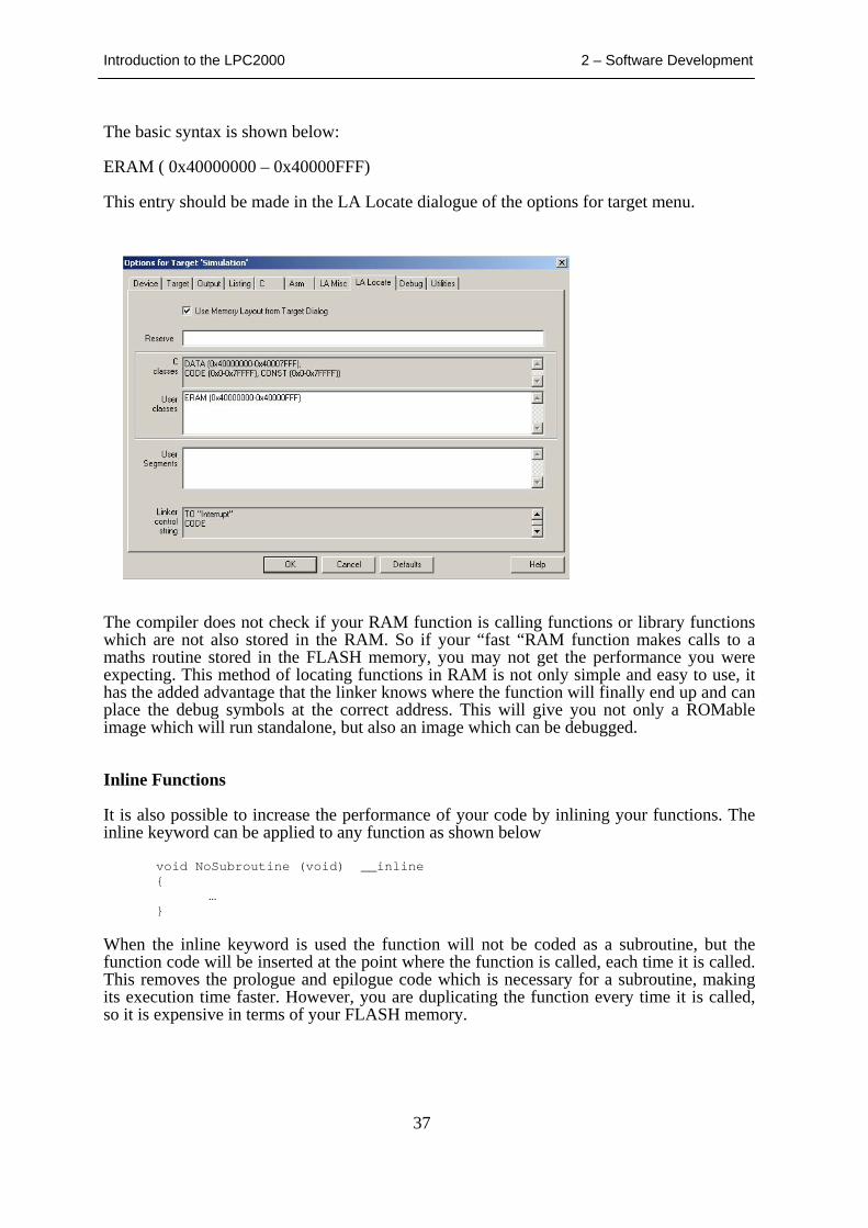
37
The basic syntax is shown below: ERAM ( 0x40000000 – 0x40000FFF) This entry should be made in the LA Locate dialogue of the options for target menu.
The compiler does not check if your RAM function is calling functions or library functions which are not also stored in the RAM. So if your “fast “RAM function makes calls to a maths routine stored in the FLASH memory, you may not get the performance you were expecting. This method of locating functions in RAM is not only simple and easy to use, it has the added advantage that the linker knows where the function will finally end up and can place the debug symbols at the correct address. This will give you not only a ROMable image which will run standalone, but also an image which can be debugged. Inline Functions It is also possible to increase the performance of your code by inlining your functions. The inline keyword can be applied to any function as shown below void NoSubroutine (void) __inline { … } When the inline keyword is used the function will not be coded as a subroutine, but the function code will be inserted at the point where the function is called, each time it is called. This removes the prologue and epilogue code which is necessary for a subroutine, making its execution time faster. However, you are duplicating the function every time it is called, so it is expensive in terms of your FLASH memory.

Introduction to the LPC2000 2 – Software Development
38
Operating System Support If you are using an operating system for the LPC2000, the OS is likely to take care of the system stacks and context switching. To avoid duplicating this by the compiler, it is possible to declare a function as a task within the operating system. This causes the compiler to just translate the code within the function and not to add the normal prologue and epilogue code which saves and restores registers to the stack. A function may be declared as a task as shown below void AnalogueSample(void) __task { …. } Fixing Objects At Absolute Locations The compiler also allows you to fix any C object, such as a variable or a function at any absolute memory location. The compiler has an extension to the C language as shown below int checksum __at 0x40000000; Variables declared using this keyword cannot be initialised by the startup code. You must also be careful to fix variables on the correct boundaries, or you will get a memory abort. (For example if an integer is located at an uneven memory address.) Inline Assembler The compiler also allows you to use ARM or THUMB Assembler instructions within a C file. This can be done as shown below: __asm { mov r15,r2; }
This can be useful if you need to use features which are not supported by the C language, for example the MRS and MSR instructions.
Introduction to the LPC2000 2 – Software Development
39
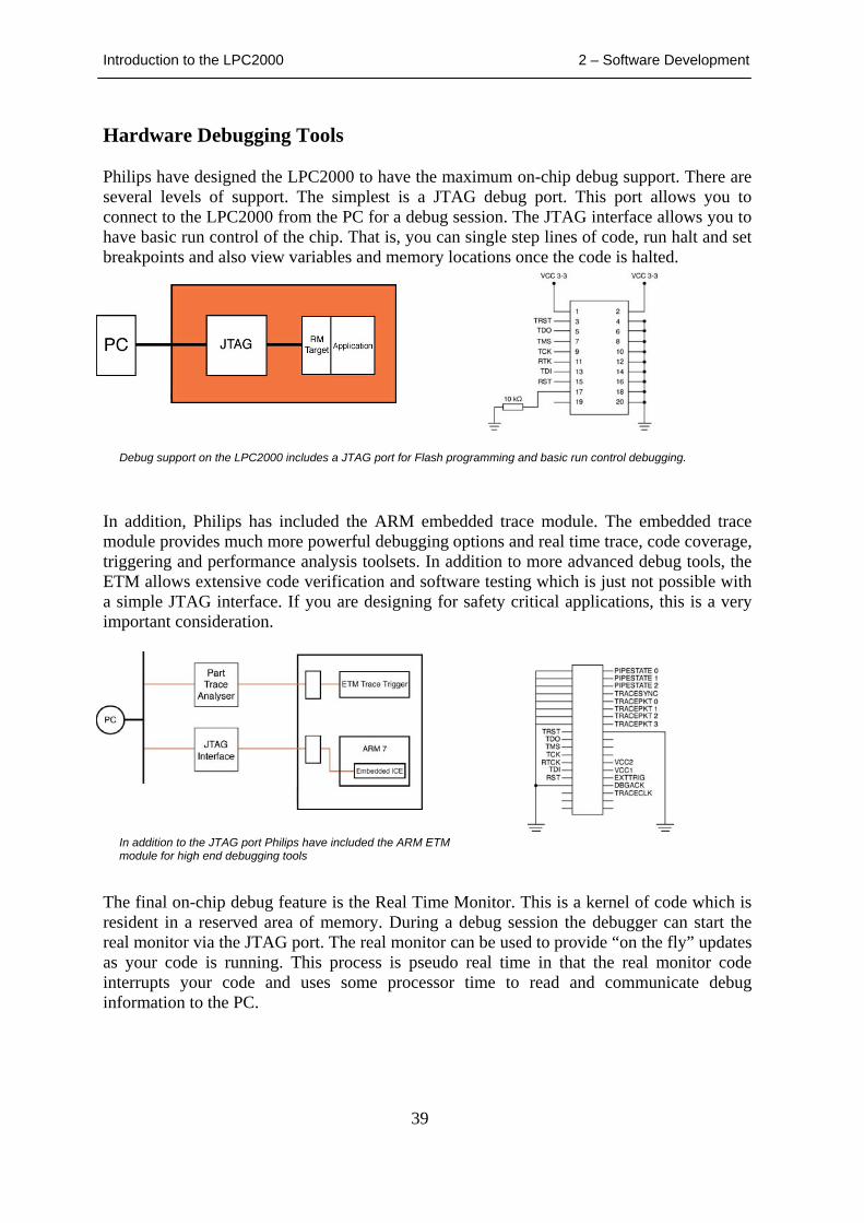
Hardware Debugging Tools Philips have designed the LPC2000 to have the maximum on-chip debug support. There are several levels of support. The simplest is a JTAG debug port. This port allows you to connect to the LPC2000 from the PC for a debug session. The JTAG interface allows you to have basic run control of the chip. That is, you can single step lines of code, run halt and set breakpoints and also view variables and memory locations once the code is halted.
In addition, Philips has included the ARM embedded trace module. The embedded trace module provides much more powerful debugging options and real time trace, code coverage, triggering and performance analysis toolsets. In addition to more advanced debug tools, the ETM allows extensive code verification and software testing which is just not possible with a simple JTAG interface. If you are designing for safety critical applications, this is a very important consideration.
The final on-chip debug feature is the Real Time Monitor. This is a kernel of code which is resident in a reserved area of memory. During a debug session the debugger can start the real monitor via the JTAG port. The real monitor can be used to provide “on the fly” updates as your code is running. This process is pseudo real time in that the real monitor code interrupts your code and uses some processor time to read and communicate debug information to the PC.
Debug support on the LPC2000 includes a JTAG port for Flash programming and basic run control debugging.
In addition to the JTAG port Philips have included the ARM ETM module for high end debugging tools
Introduction to the LPC2000 2 – Software Development
40
Important! The JTAG and ETM tools simply provide a fairly “dumb” serial debug connection to the ARM7 core. A generic ARM JTAG tool does not have any understanding of the overall LPC2000 architecture. This means that a generic tool will always enter the bootloader after reset because it does not write the “program signature” into the FLASH (this feature is discussed later) and consequently will never run your code. If you are new to the LPC2000 this is likely to catch you out and be very frustrating. Since the Keil tools are developed for ARM7 based general purpose microcontrollers MicroVision (“uVISION”) understands the LPC2000 memory architecture and will debug the device seamlessly. Even More Important As mentioned above, the JTAG port is a simple serial debug connection to the ARM7 device. It is very important to understand its behaviour during reset. If the ARM7 CPU is reset, all of the peripherals including the JTAG are reset. When this happens the ULINK debugger loses control of the chip and has to re-establish control once the LPC2000 device comes out of reset. This will take a finite number of clock cycles. While this is happening, any code which is on the chip will be run as normal. Once the ULINK gets back control of the chip, it performs a soft reset by forcing the PC back to address zero. However, the on-chip peripherals are no longer in the reset condition ie peripherals will be initialised, interrupt enabled etc. You must bear this in mind if the application you are developing could be adversely affected by this. A quick solution is to place a simple delay loop in the startup code or at the beginning of main(). After a reset occurs, the CPU will be trapped in this loop until the ULINK regains control of the chip. None of the application code will have run, leaving the LPC2000 in its initialised condition. Summary So, by the end of this section you should be able to set up a project in the Keil uVISION IDE, select the compiler and LPC2000 variant you want to use, configure the startup code, be able to interwork the ARM and THUMB instruction sets, access the LPC2000 peripherals and write C functions to handle exceptions. With this grounding we can now have a look at the LPC2000 system peripherals.

Introduction to the LPC2000 2 – Software Development
41
Introduction to the LPC2000 3 – System Peripherals
42
Chapter 3: System Peripherals Outline Now that we have some familiarity with the ARM7 core and the necessary development tools, we can begin to look at the LPC2000 devices themselves. In this section we will concentrate on the system peripherals, that is to say the features which are used to control the performance and functional features of the device. This includes the on-chip flash and SRAM memory, the external bus interface which is present on the LPC22xx devices, the phase locked loop which is used to multiply the external oscillator in order to provide a maximum of 60MHz processor clock and the power control features. Finally, we will take a look at the simplest user interrupt source, the external interrupt pins, before going on to look at the exception system in detail in the next section. Bus Structure To the programmer, the memory of all LPC2100 devices is one contiguous 32 bit address range. However, the device itself is made up of a number of buses. The ARM7 core is connected to the Advanced High performance Bus (AHB) defined by ARM. As its name implies, this is the fastest way of connecting peripheral devices to the ARM7 core. Connected to the AHB is the vector interrupt controller and a bridge to a second bus called the VLSI peripheral bus (VPB). Since the Interrupt vector controller is responsible for managing all the device interrupt sources, it is connected to the ARM7 core by the fastest bus. All the remaining user peripherals are connected to the VPB. The VBP bridge contains a clock divider, so the VPB bus can be run at a slower speed than the ARM7 core and the AHB. This is useful for two reasons. Firstly, we can run the user peripherals at a slower clock rate than the main processor to conserve power. Secondly it gives Philips the option of adding a slower peripheral to the LPC2000 family without it becoming a bottleneck on the AHB bus. Currently all the on-chip peripherals are capable of running at 60MHz so the VPB bus can be set to the same speed as the AHB bus. It is important to note that after reset the VPB divider is set to divide down the AHB clock by four, so all the on-chip peripherals will be running at ¼ the CPU clock frequency. Finally, there is a third local bus which is used to connect the on-chip Flash and RAM to the CPU. Connection of the program code and data store to the ARM7 CPU via the AHB bus is possible, but this introduces some execution stalls because of contention on the bus. Using a separate local bus removes the possibility of these stalls to give the best processor performance.
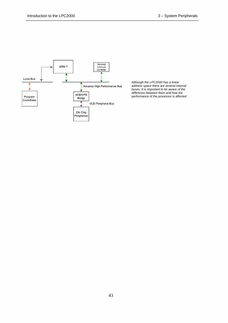
Introduction to the LPC2000 3 – System Peripherals
43
Although the LPC2000 has a linear address space there are several internal buses. It is important to be aware of the difference between them and how the performance of the processor is affected
Introduction to the LPC2000 3 – System Peripherals
44
Memory Map Despite the number of internal buses, the LPC2000 has a completely linear memory map. The general layout is shown below.
The on-chip flash is fixed at 0x00000000 upwards with the user RAM fixed at 0x4000000 upwards. The LPC2000 is pre-programmed at manufacture with a FLASH bootloader and the ARM real monitor debug program. These programs are placed in the region 0x7FFFFFF – 0x8000000. The region between 0x8000000 and 0xE000000 is reserved for external memory. Currently the LPC22xx devices are capable of addressing external memory via four chipselects each with a 16 Mbyte page.
The user peripherals located on the VPB are all mapped into the region between 0xE000000 and 0xE020000 and each peripheral is allocated a 16K memory page. Finally the Vector Interrupt Unit is located at the top of the address range at 0xFFFFF000.
The memory map of the LPC2000 includes regions for on chip flash memory user SRAM, a pre- programmed bootloader, external bus and user peripherals.
All the user peripherals are located on the VLSI peripheral bus. Each peripheral has a 16K address range for its registers.
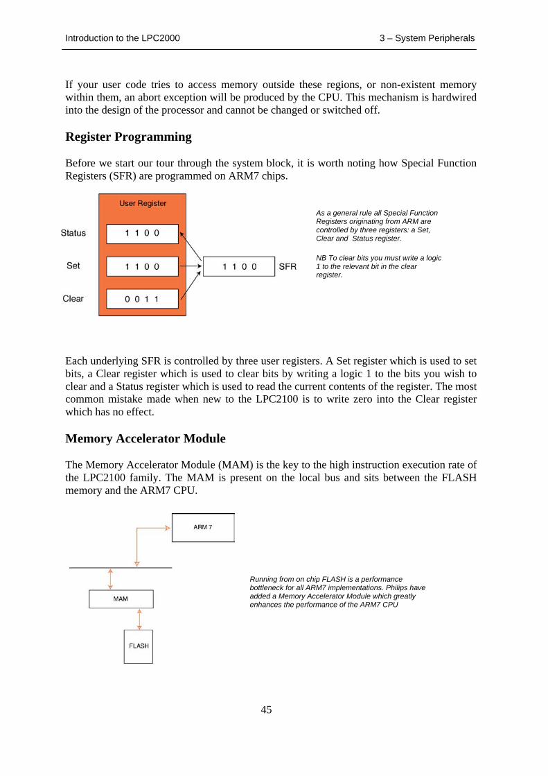
Introduction to the LPC2000 3 – System Peripherals
45
If your user code tries to access memory outside these regions, or non-existent memory within them, an abort exception will be produced by the CPU. This mechanism is hardwired into the design of the processor and cannot be changed or switched off. Register Programming Before we start our tour through the system block, it is worth noting how Special Function Registers (SFR) are programmed on ARM7 chips.
Each underlying SFR is controlled by three user registers. A Set register which is used to set bits, a Clear register which is used to clear bits by writing a logic 1 to the bits you wish to clear and a Status register which is used to read the current contents of the register. The most common mistake made when new to the LPC2100 is to write zero into the Clear register which has no effect. Memory Accelerator Module The Memory Accelerator Module (MAM) is the key to the high instruction execution rate of the LPC2100 family. The MAM is present on the local bus and sits between the FLASH memory and the ARM7 CPU.
As a general rule all Special Function Registers originating from ARM are controlled by three registers: a Set, Clear and Status register.
NB To clear bits you must write a logic 1 to the relevant bit in the clear register.
Running from on chip FLASH is a performance bottleneck for all ARM7 implementations. Philips have added a Memory Accelerator Module which greatly enhances the performance of the ARM7 CPU
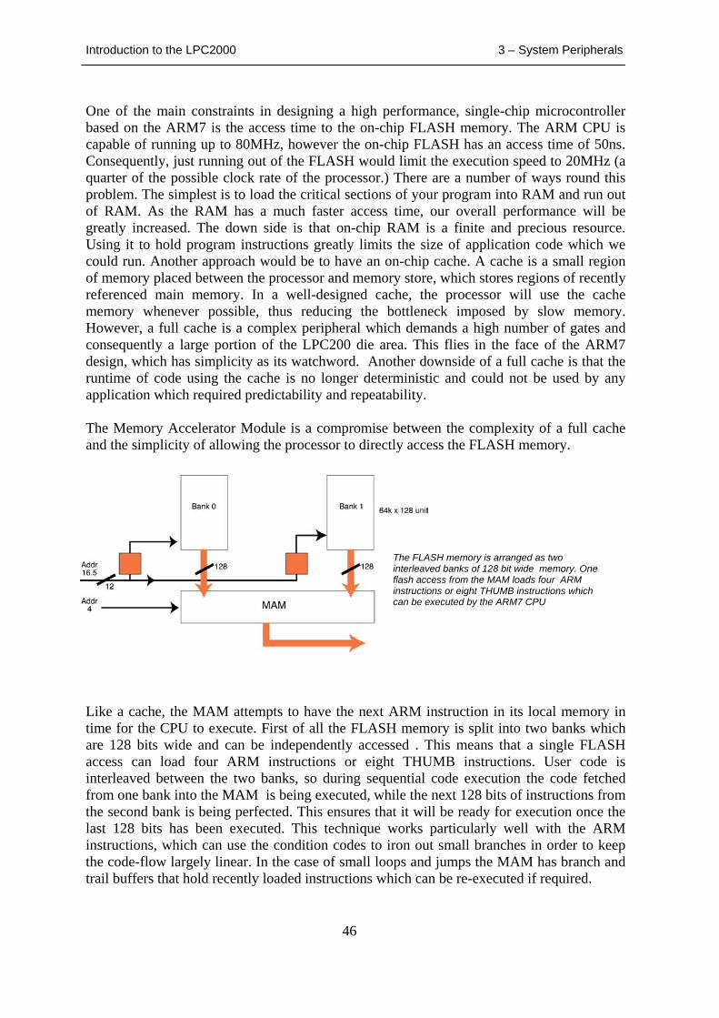
Introduction to the LPC2000 3 – System Peripherals
46
One of the main constraints in designing a high performance, single-chip microcontroller based on the ARM7 is the access time to the on-chip FLASH memory. The ARM CPU is capable of running up to 80MHz, however the on-chip FLASH has an access time of 50ns. Consequently, just running out of the FLASH would limit the execution speed to 20MHz (a quarter of the possible clock rate of the processor.) There are a number of ways round this problem. The simplest is to load the critical sections of your program into RAM and run out of RAM. As the RAM has a much faster access time, our overall performance will be greatly increased. The down side is that on-chip RAM is a finite and precious resource. Using it to hold program instructions greatly limits the size of application code which we could run. Another approach would be to have an on-chip cache. A cache is a small region of memory placed between the processor and memory store, which stores regions of recently referenced main memory. In a well-designed cache, the processor will use the cache memory whenever possible, thus reducing the bottleneck imposed by slow memory. However, a full cache is a complex peripheral which demands a high number of gates and consequently a large portion of the LPC200 die area. This flies in the face of the ARM7 design, which has simplicity as its watchword. Another downside of a full cache is that the runtime of code using the cache is no longer deterministic and could not be used by any application which required predictability and repeatability. The Memory Accelerator Module is a compromise between the complexity of a full cache and the simplicity of allowing the processor to directly access the FLASH memory.
Like a cache, the MAM attempts to have the next ARM instruction in its local memory in time for the CPU to execute. First of all the FLASH memory is split into two banks which are 128 bits wide and can be independently accessed . This means that a single FLASH access can load four ARM instructions or eight THUMB instructions. User code is interleaved between the two banks, so during sequential code execution the code fetched from one bank into the MAM is being executed, while the next 128 bits of instructions from the second bank is being perfected. This ensures that it will be ready for execution once the last 128 bits has been executed. This technique works particularly well with the ARM instructions, which can use the condition codes to iron out small branches in order to keep the code-flow largely linear. In the case of small loops and jumps the MAM has branch and trail buffers that hold recently loaded instructions which can be re-executed if required.
The FLASH memory is arranged as two interleaved banks of 128 bit wide memory. One flash access from the MAM loads four ARM instructions or eight THUMB instructions which can be executed by the ARM7 CPU
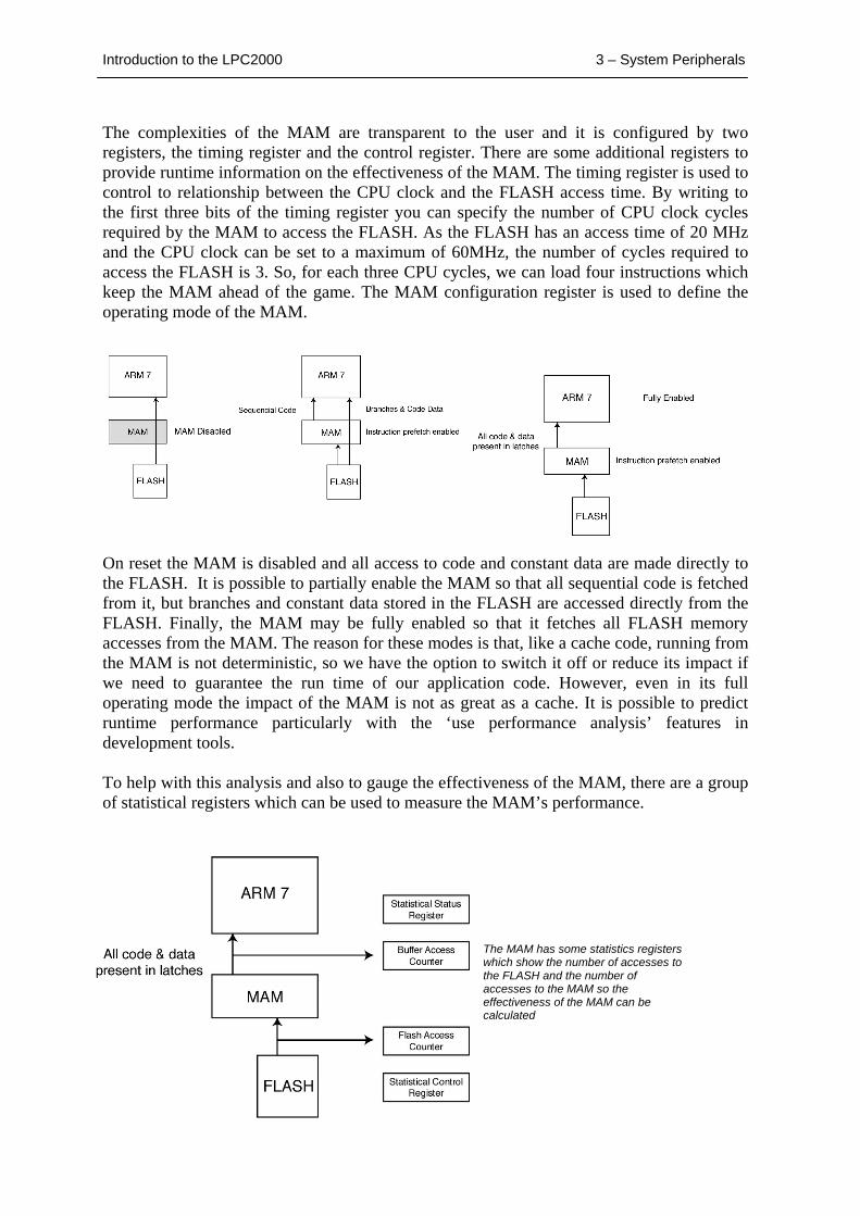
Introduction to the LPC2000 3 – System Peripherals
47
The complexities of the MAM are transparent to the user and it is configured by two registers, the timing register and the control register. There are some additional registers to provide runtime information on the effectiveness of the MAM. The timing register is used to control to relationship between the CPU clock and the FLASH access time. By writing to the first three bits of the timing register you can specify the number of CPU clock cycles required by the MAM to access the FLASH. As the FLASH has an access time of 20 MHz and the CPU clock can be set to a maximum of 60MHz, the number of cycles required to access the FLASH is 3. So, for each three CPU cycles, we can load four instructions which keep the MAM ahead of the game. The MAM configuration register is used to define the operating mode of the MAM.
On reset the MAM is disabled and all access to code and constant data are made directly to the FLASH. It is possible to partially enable the MAM so that all sequential code is fetched from it, but branches and constant data stored in the FLASH are accessed directly from the FLASH. Finally, the MAM may be fully enabled so that it fetches all FLASH memory accesses from the MAM. The reason for these modes is that, like a cache code, running from the MAM is not deterministic, so we have the option to switch it off or reduce its impact if we need to guarantee the run time of our application code. However, even in its full operating mode the impact of the MAM is not as great as a cache. It is possible to predict runtime performance particularly with the ‘use performance analysis’ features in development tools. To help with this analysis and also to gauge the effectiveness of the MAM, there are a group of statistical registers which can be used to measure the MAM’s performance.
The MAM has some statistics registers which show the number of accesses to the FLASH and the number of accesses to the MAM so the effectiveness of the MAM can be calculated

Introduction to the LPC2000 3 – System Peripherals
48
The Statistics registers are based around two counters which record the accesses made to the FLASH and the accesses made to the MAM buffers. The statistical control register can further refine the type of access which will cause the counters to increment. By configuring the statistical control register we can differentiate between code constant and instruction fetches, so it is possible to determine the instruction or data hit rate or the combined instruction and data hit rate. These metrics can give us some information on the efficacy of the MAM with our application. On the CD there is a simple example which demonstrates the use of the MAM, its statistical registers and demonstrates how vital it is to the overall performance of the LPC2000 family.
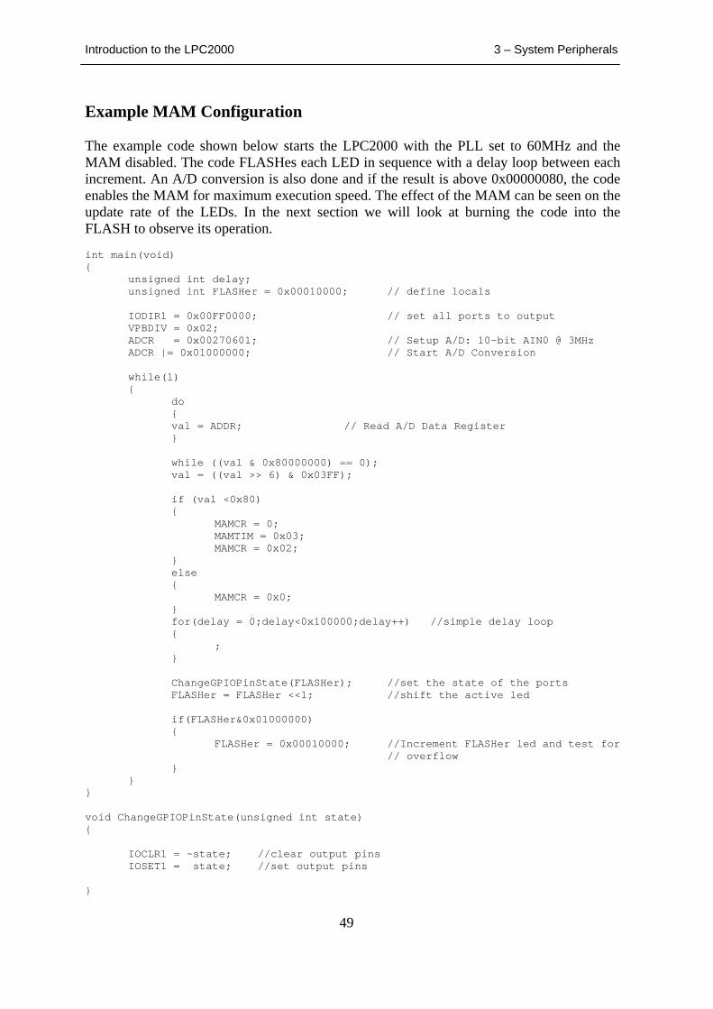
Introduction to the LPC2000 3 – System Peripherals
49
Example MAM Configuration The example code shown below starts the LPC2000 with the PLL set to 60MHz and the MAM disabled. The code FLASHes each LED in sequence with a delay loop between each increment. An A/D conversion is also done and if the result is above 0x00000080, the code enables the MAM for maximum execution speed. The effect of the MAM can be seen on the update rate of the LEDs. In the next section we will look at burning the code into the FLASH to observe its operation. int main(void) {
unsigned int delay; unsigned int FLASHer = 0x00010000; // define locals
IODIR1 = 0x00FF0000; // set all ports to output VPBDIV = 0x02; ADCR = 0x00270601; // Setup A/D: 10-bit AIN0 @ 3MHz ADCR |= 0x01000000; // Start A/D Conversion
while(1) {
do { val = ADDR; // Read A/D Data Register }
while ((val & 0x80000000) == 0); val = ((val >> 6) & 0x03FF);
if (val <0x80) {
MAMCR = 0; MAMTIM = 0x03; MAMCR = 0x02;
} else {
MAMCR = 0x0; } for(delay = 0;delay<0x100000;delay++) //simple delay loop {
; }
ChangeGPIOPinState(FLASHer); //set the state of the ports FLASHer = FLASHer <<1; //shift the active led
if(FLASHer&0x01000000) {
FLASHer = 0x00010000; //Increment FLASHer led and test for // overflow
} }
} void ChangeGPIOPinState(unsigned int state) {
IOCLR1 = ~state; //clear output pins IOSET1 = state; //set output pins
}
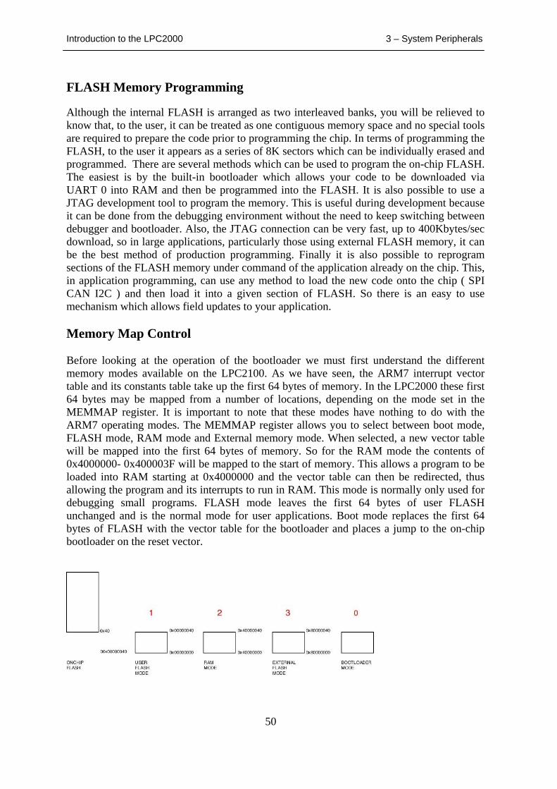
Introduction to the LPC2000 3 – System Peripherals
50
FLASH Memory Programming Although the internal FLASH is arranged as two interleaved banks, you will be relieved to know that, to the user, it can be treated as one contiguous memory space and no special tools are required to prepare the code prior to programming the chip. In terms of programming the FLASH, to the user it appears as a series of 8K sectors which can be individually erased and programmed. There are several methods which can be used to program the on-chip FLASH. The easiest is by the built-in bootloader which allows your code to be downloaded via UART 0 into RAM and then be programmed into the FLASH. It is also possible to use a JTAG development tool to program the memory. This is useful during development because it can be done from the debugging environment without the need to keep switching between debugger and bootloader. Also, the JTAG connection can be very fast, up to 400Kbytes/sec download, so in large applications, particularly those using external FLASH memory, it can be the best method of production programming. Finally it is also possible to reprogram sections of the FLASH memory under command of the application already on the chip. This, in application programming, can use any method to load the new code onto the chip ( SPI CAN I2C ) and then load it into a given section of FLASH. So there is an easy to use mechanism which allows field updates to your application. Memory Map Control Before looking at the operation of the bootloader we must first understand the different memory modes available on the LPC2100. As we have seen, the ARM7 interrupt vector table and its constants table take up the first 64 bytes of memory. In the LPC2000 these first 64 bytes may be mapped from a number of locations, depending on the mode set in the MEMMAP register. It is important to note that these modes have nothing to do with the ARM7 operating modes. The MEMMAP register allows you to select between boot mode, FLASH mode, RAM mode and External memory mode. When selected, a new vector table will be mapped into the first 64 bytes of memory. So for the RAM mode the contents of 0x4000000- 0x400003F will be mapped to the start of memory. This allows a program to be loaded into RAM starting at 0x4000000 and the vector table can then be redirected, thus allowing the program and its interrupts to run in RAM. This mode is normally only used for debugging small programs. FLASH mode leaves the first 64 bytes of user FLASH unchanged and is the normal mode for user applications. Boot mode replaces the first 64 bytes of FLASH with the vector table for the bootloader and places a jump to the on-chip bootloader on the reset vector.
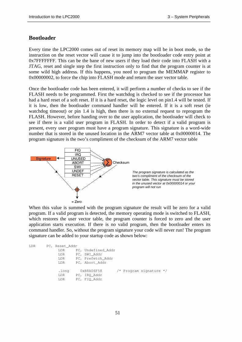
Introduction to the LPC2000 3 – System Peripherals
51
Bootloader Every time the LPC2000 comes out of reset its memory map will be in boot mode, so the instruction on the reset vector will cause it to jump into the bootloader code entry point at 0x7FFFFFFF. This can be the bane of new users if they load their code into FLASH with a JTAG, reset and single step the first instruction only to find that the program counter is at some wild high address. If this happens, you need to program the MEMMAP register to 0x00000002, to force the chip into FLASH mode and return the user vector table. Once the bootloader code has been entered, it will perform a number of checks to see if the FLASH needs to be programmed. First the watchdog is checked to see if the processor has had a hard reset of a soft reset. If it is a hard reset, the logic level on pin1.4 will be tested. If it is low, then the bootloader command handler will be entered. If it is a soft reset (ie watchdog timeout) or pin 1.4 is high, then there is no external request to reprogram the FLASH. However, before handing over to the user application, the bootloader will check to see if there is a valid user program in FLASH. In order to detect if a valid program is present, every user program must have a program signature. This signature is a word-wide number that is stored in the unused location in the ARM7 vector table at 0x00000014. The program signature is the two’s compliment of the checksum of the ARM7 vector table
When this value is summed with the program signature the result will be zero for a valid program. If a valid program is detected, the memory operating mode is switched to FLASH, which restores the user vector table, the program counter is forced to zero and the user application starts execution. If there is no valid program, then the bootloader enters its command handler. So, without the program signature your code will never run! The program signature can be added to your startup code as shown below: LDR PC, Reset_Addr LDR PC, Undefined_Addr LDR PC, SWI_Addr LDR PC, Prefetch_Addr LDR PC, Abort_Addr .long 0xB8A06F58 /* Program signature */ LDR PC, IRQ_Addr LDR PC, FIQ_Addr
The program signature is calculated as the two’s compliment of the checksum of the vector table. This signature must be stored in the unused vector at 0x00000014 or your program will not run
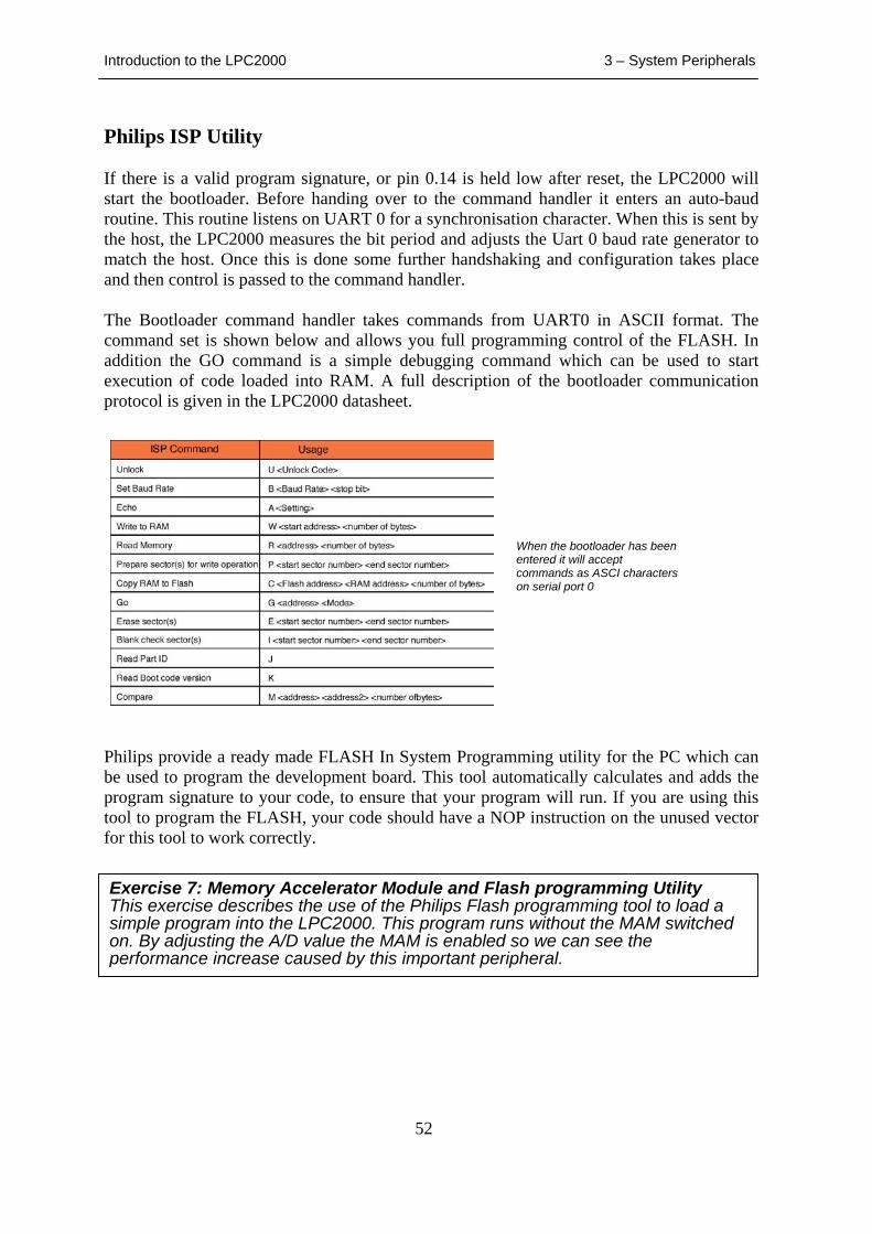
Introduction to the LPC2000 3 – System Peripherals
52
Philips ISP Utility If there is a valid program signature, or pin 0.14 is held low after reset, the LPC2000 will start the bootloader. Before handing over to the command handler it enters an auto-baud routine. This routine listens on UART 0 for a synchronisation character. When this is sent by the host, the LPC2000 measures the bit period and adjusts the Uart 0 baud rate generator to match the host. Once this is done some further handshaking and configuration takes place and then control is passed to the command handler. The Bootloader command handler takes commands from UART0 in ASCII format. The command set is shown below and allows you full programming control of the FLASH. In addition the GO command is a simple debugging command which can be used to start execution of code loaded into RAM. A full description of the bootloader communication protocol is given in the LPC2000 datasheet.
Philips provide a ready made FLASH In System Programming utility for the PC which can be used to program the development board. This tool automatically calculates and adds the program signature to your code, to ensure that your program will run. If you are using this tool to program the FLASH, your code should have a NOP instruction on the unused vector for this tool to work correctly.
When the bootloader has been entered it will accept commands as ASCI characters on serial port 0
Exercise 7: Memory Accelerator Module and Flash programming Utility This exercise describes the use of the Philips Flash programming tool to load a simple program into the LPC2000. This program runs without the MAM switched on. By adjusting the A/D value the MAM is enabled so we can see the performance increase caused by this important peripheral.
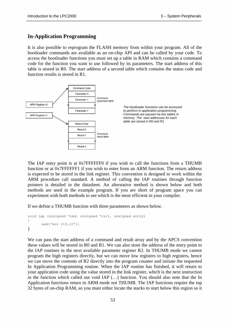
Introduction to the LPC2000 3 – System Peripherals
53
In-Application Programming It is also possible to reprogram the FLASH memory from within your program. All of the bootloader commands are available as an on-chip API and can be called by your code. To access the bootloader functions you must set up a table in RAM which contains a command code for the function you want to use followed by its parameters. The start address of this table is stored in R0. The start address of a second table which contains the status code and function results is stored in R1.
The IAP entry point is at 0x7FFFFFF0 if you wish to call the functions from a THUMB function or at 0x7FFFFFF1 if you wish to enter from an ARM function. The return address is expected to be stored in the link register. This convention is designed to work within the ARM procedure call standard. A method of calling the IAP routines through function pointers is detailed in the datasheet. An alternative method is shown below and both methods are used in the example program. If you are short of program space you can experiment with both methods to see which is the most efficient in your compiler. If we define a THUMB function with three parameters as shown below. void iap (unsigned *cmd, unsigned *rslt, unsigned entry) { asm("mov r15,r2");
} We can pass the start address of a command and result array and by the APCS convention these values will be stored in R0 and R1. We can also store the address of the entry point to the IAP routines in the next available parameter register R2. In THUMB mode we cannot program the high registers directly, but we can move low registers to high registers, hence we can move the contents of R2 directly into the program counter and initiate the requested In Application Programming routine. When the IAP routine has finished, it will return to your application code using the value stored in the link register, which is the next instruction in the function which called our void IAP (…) function. You should also note that the In Application functions return in ARM mode not THUMB. The IAP functions require the top 32 bytes of on-chip RAM, so you must either locate the stacks to start below this region so it
The bootloader functions can be accessed to perform In application programming. Commands are passed via two tables in memory. The start addresses for each table are stored in R0 and R1
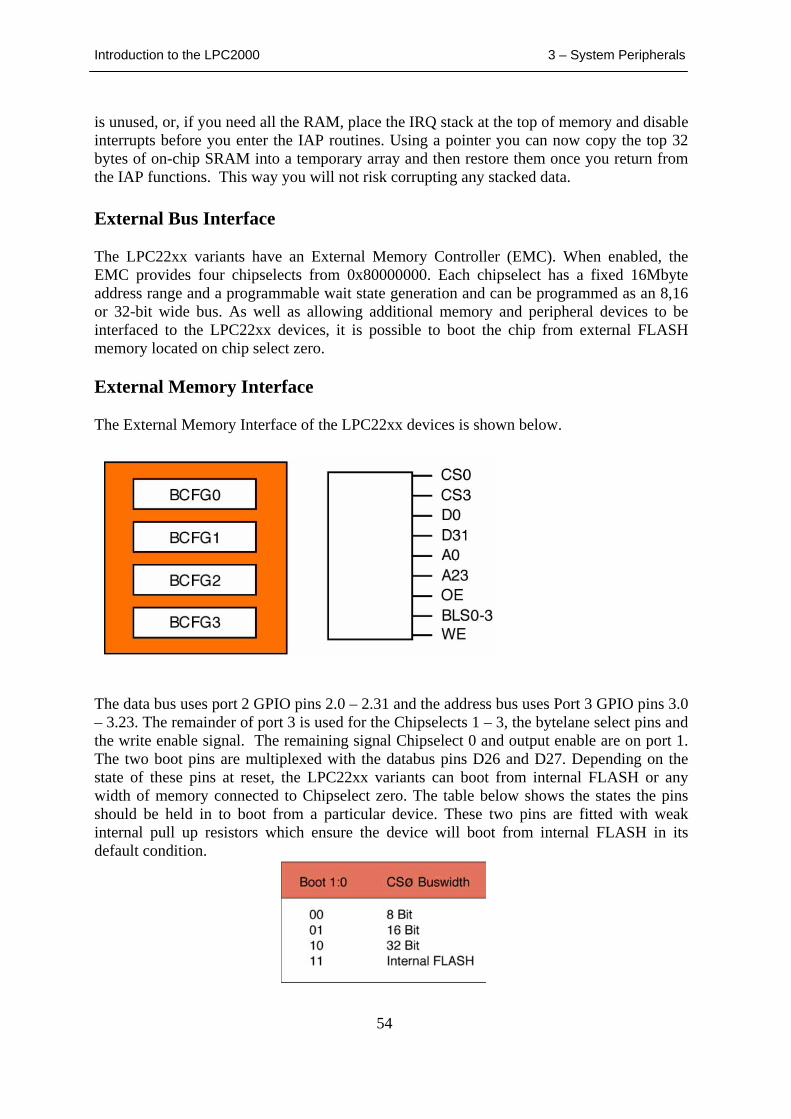
Introduction to the LPC2000 3 – System Peripherals
54
is unused, or, if you need all the RAM, place the IRQ stack at the top of memory and disable interrupts before you enter the IAP routines. Using a pointer you can now copy the top 32 bytes of on-chip SRAM into a temporary array and then restore them once you return from the IAP functions. This way you will not risk corrupting any stacked data. External Bus Interface The LPC22xx variants have an External Memory Controller (EMC). When enabled, the EMC provides four chipselects from 0x80000000. Each chipselect has a fixed 16Mbyte address range and a programmable wait state generation and can be programmed as an 8,16 or 32-bit wide bus. As well as allowing additional memory and peripheral devices to be interfaced to the LPC22xx devices, it is possible to boot the chip from external FLASH memory located on chip select zero. External Memory Interface The External Memory Interface of the LPC22xx devices is shown below.
The data bus uses port 2 GPIO pins 2.0 – 2.31 and the address bus uses Port 3 GPIO pins 3.0 – 3.23. The remainder of port 3 is used for the Chipselects 1 – 3, the bytelane select pins and the write enable signal. The remaining signal Chipselect 0 and output enable are on port 1. The two boot pins are multiplexed with the databus pins D26 and D27. Depending on the state of these pins at reset, the LPC22xx variants can boot from internal FLASH or any width of memory connected to Chipselect zero. The table below shows the states the pins should be held in to boot from a particular device. These two pins are fitted with weak internal pull up resistors which ensure the device will boot from internal FLASH in its default condition.
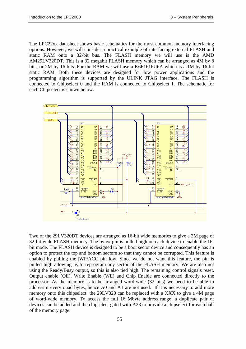
Introduction to the LPC2000 3 – System Peripherals
55
The LPC22xx datasheet shows basic schematics for the most common memory interfacing options. However, we will consider a practical example of interfacing external FLASH and static RAM onto a 32-bit bus. The FLASH memory we will use is the AMD AM29LV320DT. This is a 32 megabit FLASH memory which can be arranged as 4M by 8 bits, or 2M by 16 bits. For the RAM we will use a K6F1616U6A which is a 1M by 16 bit static RAM. Both these devices are designed for low power applications and the programming algorithm is supported by the ULINK JTAG interface. The FLASH is connected to Chipselect 0 and the RAM is connected to Chipselect 1. The schematic for each Chipselect is shown below.
Two of the 29LV320DT devices are arranged as 16-bit wide memories to give a 2M page of 32-bit wide FLASH memory. The byte# pin is pulled high on each device to enable the 16-bit mode. The FLASH device is designed to be a boot sector device and consequently has an option to protect the top and bottom sectors so that they cannot be corrupted. This feature is enabled by pulling the |WP/ACC pin low. Since we do not want this feature, the pin is pulled high allowing us to reprogram any sector of the FLASH memory. We are also not using the Ready/Busy output, so this is also tied high. The remaining control signals reset, Output enable (OE), Write Enable (WE) and Chip Enable are connected directly to the processor. As the memory is to be arranged word-wide (32 bits) we need to be able to address it every quad bytes, hence A0 and A1 are not used. If it is necessary to add more memory onto this chipselect the 29LV320 can be replaced with a XXX to give a 4M page of word-wide memory. To access the full 16 Mbyte address range, a duplicate pair of devices can be added and the chipselect gated with A23 to provide a chipselect for each half of the memory page.
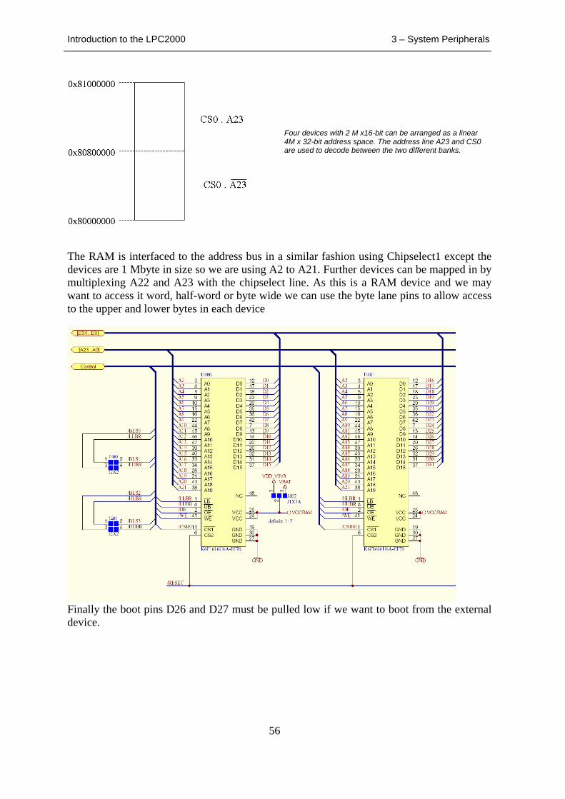
Introduction to the LPC2000 3 – System Peripherals
56
The RAM is interfaced to the address bus in a similar fashion using Chipselect1 except the devices are 1 Mbyte in size so we are using A2 to A21. Further devices can be mapped in by multiplexing A22 and A23 with the chipselect line. As this is a RAM device and we may want to access it word, half-word or byte wide we can use the byte lane pins to allow access to the upper and lower bytes in each device
Finally the boot pins D26 and D27 must be pulled low if we want to boot from the external device.
Four devices with 2 M x16-bit can be arranged as a linear 4M x 32-bit address space. The address line A23 and CS0 are used to decode between the two different banks.
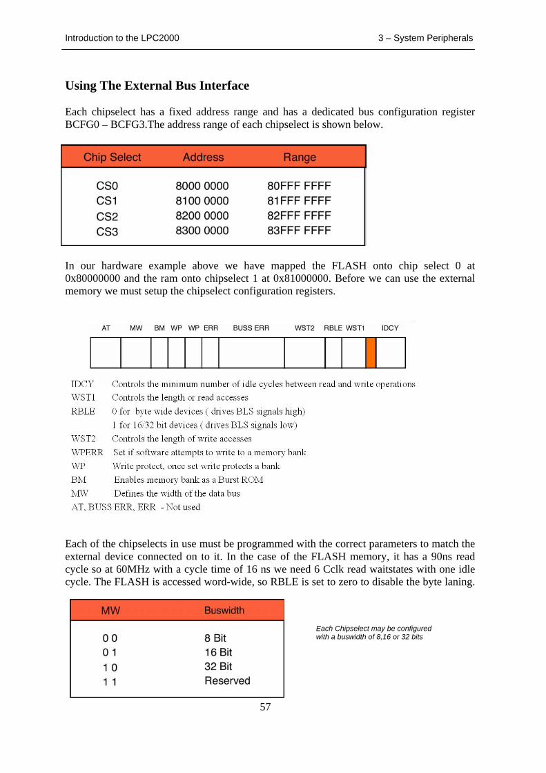
Introduction to the LPC2000 3 – System Peripherals
57
Using The External Bus Interface Each chipselect has a fixed address range and has a dedicated bus configuration register BCFG0 – BCFG3.The address range of each chipselect is shown below.
In our hardware example above we have mapped the FLASH onto chip select 0 at 0x80000000 and the ram onto chipselect 1 at 0x81000000. Before we can use the external memory we must setup the chipselect configuration registers.
Each of the chipselects in use must be programmed with the correct parameters to match the external device connected on to it. In the case of the FLASH memory, it has a 90ns read cycle so at 60MHz with a cycle time of 16 ns we need 6 Cclk read waitstates with one idle cycle. The FLASH is accessed word-wide, so RBLE is set to zero to disable the byte laning.
Each Chipselect may be configured with a buswidth of 8,16 or 32 bits
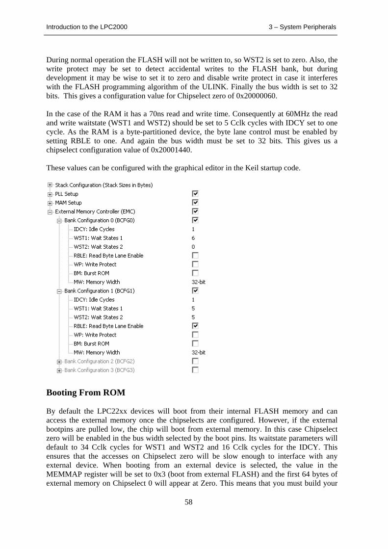
Introduction to the LPC2000 3 – System Peripherals
58
During normal operation the FLASH will not be written to, so WST2 is set to zero. Also, the write protect may be set to detect accidental writes to the FLASH bank, but during development it may be wise to set it to zero and disable write protect in case it interferes with the FLASH programming algorithm of the ULINK. Finally the bus width is set to 32 bits. This gives a configuration value for Chipselect zero of 0x20000060. In the case of the RAM it has a 70ns read and write time. Consequently at 60MHz the read and write waitstate (WST1 and WST2) should be set to 5 Cclk cycles with IDCY set to one cycle. As the RAM is a byte-partitioned device, the byte lane control must be enabled by setting RBLE to one. And again the bus width must be set to 32 bits. This gives us a chipselect configuration value of 0x20001440. These values can be configured with the graphical editor in the Keil startup code.
Booting From ROM By default the LPC22xx devices will boot from their internal FLASH memory and can access the external memory once the chipselects are configured. However, if the external bootpins are pulled low, the chip will boot from external memory. In this case Chipselect zero will be enabled in the bus width selected by the boot pins. Its waitstate parameters will default to 34 Cclk cycles for WST1 and WST2 and 16 Cclk cycles for the IDCY. This ensures that the accesses on Chipselect zero will be slow enough to interface with any external device. When booting from an external device is selected, the value in the MEMMAP register will be set to 0x3 (boot from external FLASH) and the first 64 bytes of external memory on Chipselect 0 will appear at Zero. This means that you must build your
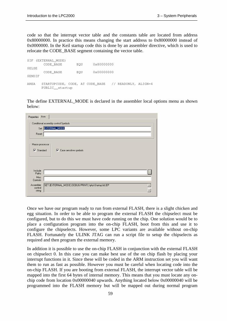
Introduction to the LPC2000 3 – System Peripherals
59
code so that the interrupt vector table and the constants table are located from address 0x80000000. In practice this means changing the start address to 0x80000000 instead of 0x0000000. In the Keil startup code this is done by an assembler directive, which is used to relocate the CODE_BASE segment containing the vector table. $IF (EXTERNAL_MODE) CODE_BASE EQU 0x80000000 $ELSE CODE_BASE EQU 0x00000000 $ENDIF AREA STARTUPCODE, CODE, AT CODE_BASE // READONLY, ALIGN=4 PUBLIC__startup The define EXTERNAL_MODE is declared in the assembler local options menu as shown below:
Once we have our program ready to run from external FLASH, there is a slight chicken and egg situation. In order to be able to program the external FLASH the chipselect must be configured, but to do this we must have code running on the chip. One solution would be to place a configuration program into the on-chip FLASH, boot from this and use it to configure the chipselects. However, some LPC variants are available without on-chip FLASH. Fortunately the ULINK JTAG can run a script file to setup the chipselects as required and then program the external memory. In addition it is possible to use the on-chip FLASH in conjunction with the external FLASH on chipselect 0. In this case you can make best use of the on chip flash by placing your interrupt functions in it. Since these will be coded in the ARM instruction set you will want them to run as fast as possible. However you must be careful when locating code into the on-chip FLASH. If you are booting from external FLASH, the interrupt vector table will be mapped into the first 64 bytes of internal memory. This means that you must locate any on-chip code from location 0x00000040 upwards. Anything located below 0x00000040 will be programmed into the FLASH memory but will be mapped out during normal program
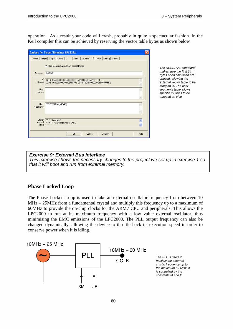
Introduction to the LPC2000 3 – System Peripherals
60
operation. As a result your code will crash, probably in quite a spectacular fashion. In the Keil compiler this can be achieved by reserving the vector table bytes as shown below
Phase Locked Loop The Phase Locked Loop is used to take an external oscillator frequency from between 10 MHz – 25MHz from a fundamental crystal and multiply this frequency up to a maximum of 60MHz to provide the on-chip clocks for the ARM7 CPU and peripherals. This allows the LPC2000 to run at its maximum frequency with a low value external oscillator, thus minimising the EMC emissions of the LPC2000. The PLL output frequency can also be changed dynamically, allowing the device to throttle back its execution speed in order to conserve power when it is idling.
The PLL is used to multiply the external crystal frequency up to the maximum 60 MHz. It is controlled by the constants M and P
Exercise 9: External Bus InterfaceThis exercise shows the necessary changes to the project we set up in exercise 1 so that it will boot and run from external memory.
The RESERVE command makes sure the first 64 bytes of on chip flash are unused, allowing the external vector table to be mapped in. The user segments table allows specific routines to be mapped on chip
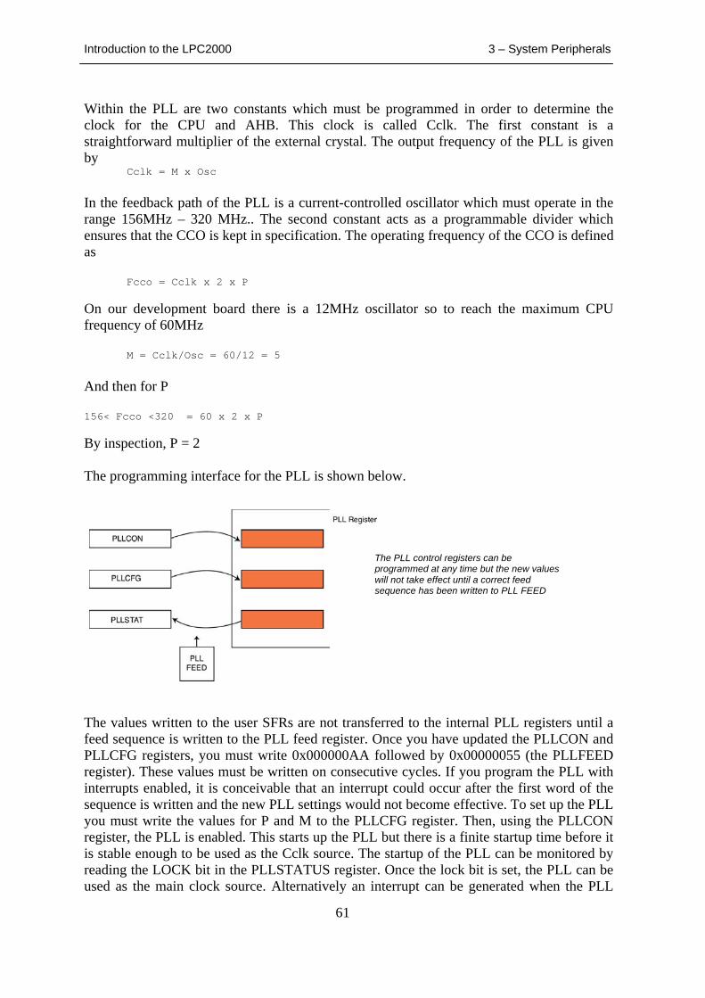
Introduction to the LPC2000 3 – System Peripherals
61
Within the PLL are two constants which must be programmed in order to determine the clock for the CPU and AHB. This clock is called Cclk. The first constant is a straightforward multiplier of the external crystal. The output frequency of the PLL is given by Cclk = M x Osc
In the feedback path of the PLL is a current-controlled oscillator which must operate in the range 156MHz – 320 MHz.. The second constant acts as a programmable divider which ensures that the CCO is kept in specification. The operating frequency of the CCO is defined as Fcco = Cclk x 2 x P
On our development board there is a 12MHz oscillator so to reach the maximum CPU frequency of 60MHz M = Cclk/Osc = 60/12 = 5
And then for P 156< Fcco <320 = 60 x 2 x P
By inspection, P = 2 The programming interface for the PLL is shown below.
The values written to the user SFRs are not transferred to the internal PLL registers until a feed sequence is written to the PLL feed register. Once you have updated the PLLCON and PLLCFG registers, you must write 0x000000AA followed by 0x00000055 (the PLLFEED register). These values must be written on consecutive cycles. If you program the PLL with interrupts enabled, it is conceivable that an interrupt could occur after the first word of the sequence is written and the new PLL settings would not become effective. To set up the PLL you must write the values for P and M to the PLLCFG register. Then, using the PLLCON register, the PLL is enabled. This starts up the PLL but there is a finite startup time before it is stable enough to be used as the Cclk source. The startup of the PLL can be monitored by reading the LOCK bit in the PLLSTATUS register. Once the lock bit is set, the PLL can be used as the main clock source. Alternatively an interrupt can be generated when the PLL
The PLL control registers can be programmed at any time but the new values will not take effect until a correct feed sequence has been written to PLL FEED
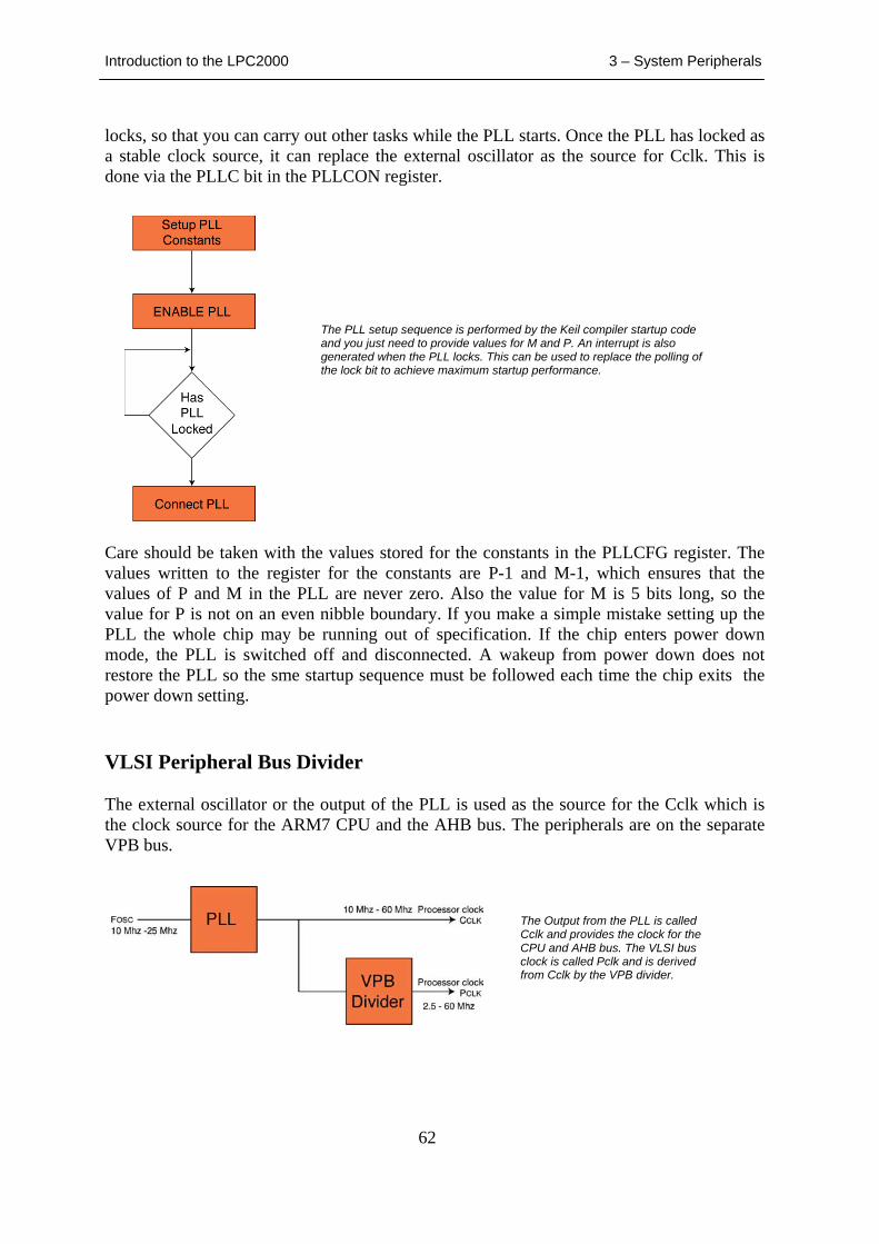
Introduction to the LPC2000 3 – System Peripherals
62
locks, so that you can carry out other tasks while the PLL starts. Once the PLL has locked as a stable clock source, it can replace the external oscillator as the source for Cclk. This is done via the PLLC bit in the PLLCON register.
Care should be taken with the values stored for the constants in the PLLCFG register. The values written to the register for the constants are P-1 and M-1, which ensures that the values of P and M in the PLL are never zero. Also the value for M is 5 bits long, so the value for P is not on an even nibble boundary. If you make a simple mistake setting up the PLL the whole chip may be running out of specification. If the chip enters power down mode, the PLL is switched off and disconnected. A wakeup from power down does not restore the PLL so the sme startup sequence must be followed each time the chip exits the power down setting. VLSI Peripheral Bus Divider The external oscillator or the output of the PLL is used as the source for the Cclk which is the clock source for the ARM7 CPU and the AHB bus. The peripherals are on the separate VPB bus.
The Output from the PLL is called Cclk and provides the clock for the CPU and AHB bus. The VLSI bus clock is called Pclk and is derived from Cclk by the VPB divider.
The PLL setup sequence is performed by the Keil compiler startup code and you just need to provide values for M and P. An interrupt is also generated when the PLL locks. This can be used to replace the polling of the lock bit to achieve maximum startup performance.
Introduction to the LPC2000 3 – System Peripherals
63
The clock on the VPB bus is called Pclk. This clock is derived from Cclk via the VPB bridge. The VPB bridge contains a divider which can divide down the Cclk by a factor of 1,2 or 4. The VPB divider register can be programmed by your application at any time. At reset it is set to the maximum value of four, so the Pclk is running at a quarter of the Cclk value at startup. Currently all the peripherals on the LPC2000 derivatives can run at the full 60MHz, so the VPB divider is principally used for power-saving by running the VPB clock at the slowest speed acceptable for your application. Example Code: PLL And VPB Configuration The code below demonstrates how to configure the PLL to give 60MHz Cclk and 30 MHz Pclk with an external crystal of 12MHz. void init_PLL(void) {
PLLCFG = 0x00000024; // Set multiplier and divider of PLL to // give 60.00 MHz
PLLCON = 0x00000001; // Enable the PLL
PLLFEED = 0x000000AA; // Update PLL registers with feed sequence PLLFEED = 0x00000055;
while (!(PLLSTAT & 0x00000400)); // test Lock bit
PLLCON = 0x00000003; // Connect the PLL
PLLFEED = 0x000000AA; //Update PLL registers PLLFEED = 0x00000055;
VPBDIV = 0x00000002; //Set the VLSI peripheral bus to 30.000MHz
}
Exercise 10: Phase Locked LoopIn this exercise we configure the PLL to generate a Cclk of 60MHz and a Pclk of 30MHz
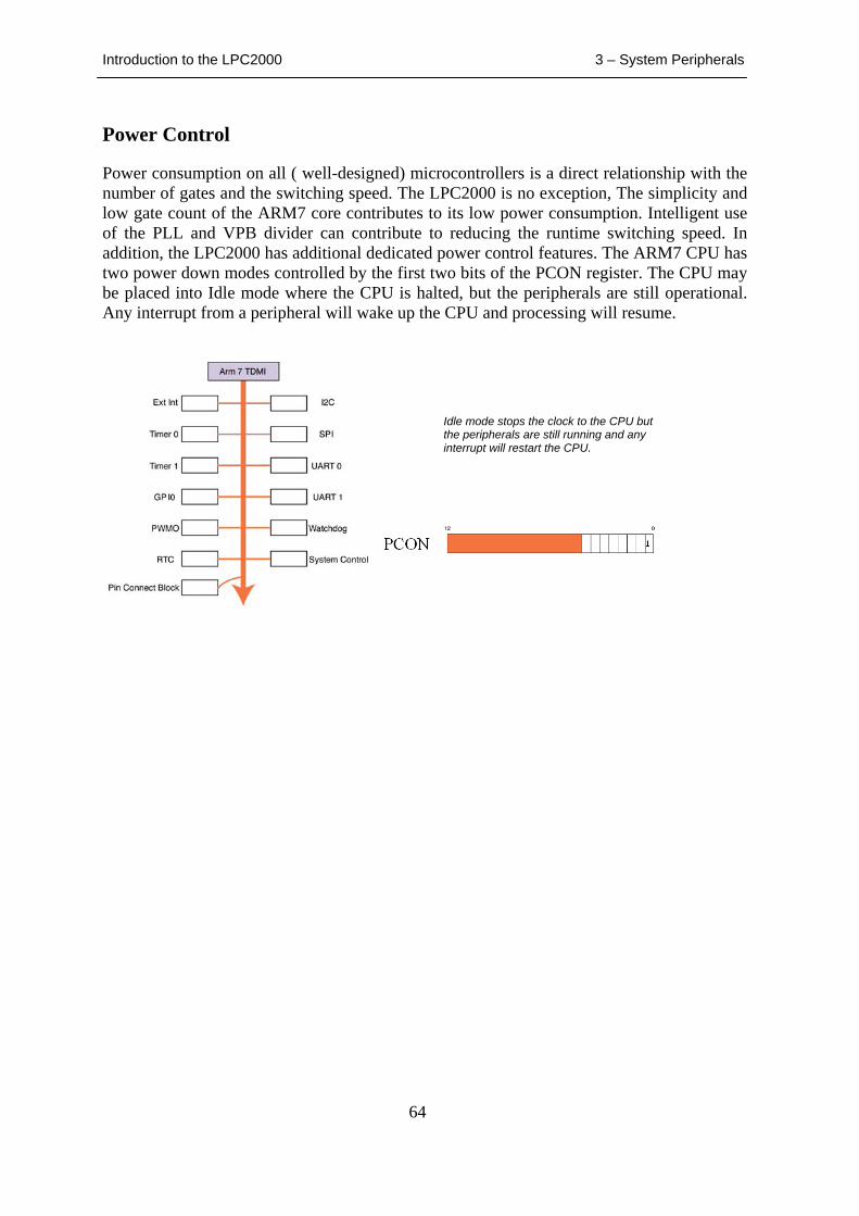
Introduction to the LPC2000 3 – System Peripherals
64
Power Control Power consumption on all ( well-designed) microcontrollers is a direct relationship with the number of gates and the switching speed. The LPC2000 is no exception, The simplicity and low gate count of the ARM7 core contributes to its low power consumption. Intelligent use of the PLL and VPB divider can contribute to reducing the runtime switching speed. In addition, the LPC2000 has additional dedicated power control features. The ARM7 CPU has two power down modes controlled by the first two bits of the PCON register. The CPU may be placed into Idle mode where the CPU is halted, but the peripherals are still operational. Any interrupt from a peripheral will wake up the CPU and processing will resume.
Idle mode stops the clock to the CPU but the peripherals are still running and any interrupt will restart the CPU.
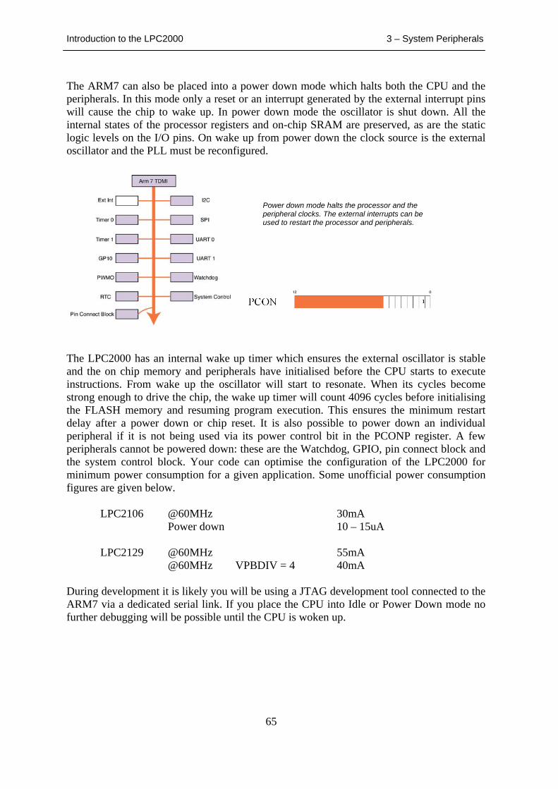
Introduction to the LPC2000 3 – System Peripherals
65
The ARM7 can also be placed into a power down mode which halts both the CPU and the peripherals. In this mode only a reset or an interrupt generated by the external interrupt pins will cause the chip to wake up. In power down mode the oscillator is shut down. All the internal states of the processor registers and on-chip SRAM are preserved, as are the static logic levels on the I/O pins. On wake up from power down the clock source is the external oscillator and the PLL must be reconfigured.
The LPC2000 has an internal wake up timer which ensures the external oscillator is stable and the on chip memory and peripherals have initialised before the CPU starts to execute instructions. From wake up the oscillator will start to resonate. When its cycles become strong enough to drive the chip, the wake up timer will count 4096 cycles before initialising the FLASH memory and resuming program execution. This ensures the minimum restart delay after a power down or chip reset. It is also possible to power down an individual peripheral if it is not being used via its power control bit in the PCONP register. A few peripherals cannot be powered down: these are the Watchdog, GPIO, pin connect block and the system control block. Your code can optimise the configuration of the LPC2000 for minimum power consumption for a given application. Some unofficial power consumption figures are given below. LPC2106 @60MHz 30mA Power down 10 – 15uA LPC2129 @60MHz 55mA @60MHz VPBDIV = 4 40mA During development it is likely you will be using a JTAG development tool connected to the ARM7 via a dedicated serial link. If you place the CPU into Idle or Power Down mode no further debugging will be possible until the CPU is woken up.
Power down mode halts the processor and the peripheral clocks. The external interrupts can be used to restart the processor and peripherals.
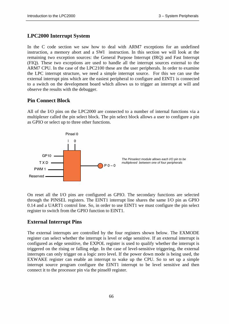
Introduction to the LPC2000 3 – System Peripherals
66
LPC2000 Interrupt System In the C code section we saw how to deal with ARM7 exceptions for an undefined instruction, a memory abort and a SWI instruction. In this section we will look at the remaining two exception sources: the General Purpose Interrupt (IRQ) and Fast Interrupt (FIQ). These two exceptions are used to handle all the interrupt sources external to the ARM7 CPU. In the case of the LPC2100 these are the user peripherals. In order to examine the LPC interrupt structure, we need a simple interrupt source. For this we can use the external interrupt pins which are the easiest peripheral to configure and EINT1 is connected to a switch on the development board which allows us to trigger an interrupt at will and observe the results with the debugger. Pin Connect Block All of the I/O pins on the LPC2000 are connected to a number of internal functions via a multiplexer called the pin select block. The pin select block allows a user to configure a pin as GPIO or select up to three other functions.
On reset all the I/O pins are configured as GPIO. The secondary functions are selected through the PINSEL registers. The EINT1 interrupt line shares the same I/O pin as GPIO 0.14 and a UART1 control line. So, in order to use EINT1 we must configure the pin select register to switch from the GPIO function to EINT1. External Interrupt Pins The external interrupts are controlled by the four registers shown below. The EXMODE register can select whether the interrupt is level or edge sensitive. If an external interrupt is configured as edge sensitive, the EXPOL register is used to qualify whether the interrupt is triggered on the rising or falling edge. In the case of level-sensitive triggering, the external interrupts can only trigger on a logic zero level. If the power down mode is being used, the EXWAKE register can enable an interrupt to wake up the CPU. So to set up a simple interrupt source program configure the EINT1 interrupt to be level sensitive and then connect it to the processor pin via the pinsel0 register.
The Pinselect module allows each I/O pin to be multiplexed between one of four peripherals
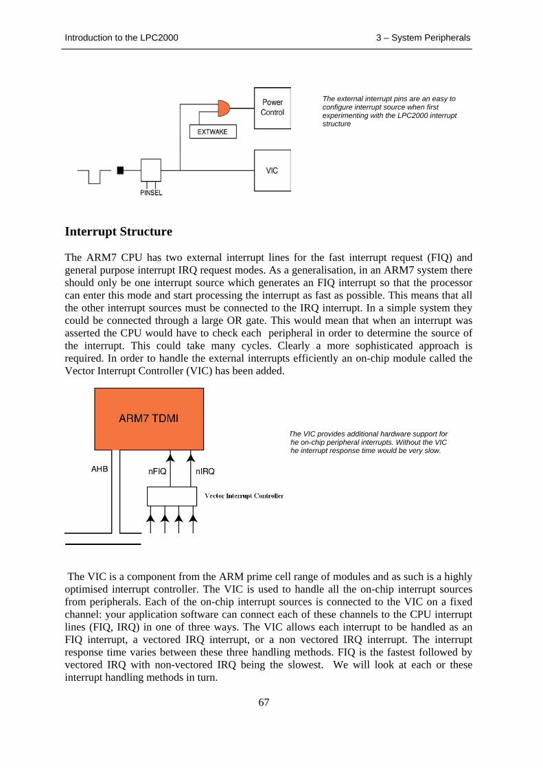
Introduction to the LPC2000 3 – System Peripherals
67
Interrupt Structure The ARM7 CPU has two external interrupt lines for the fast interrupt request (FIQ) and general purpose interrupt IRQ request modes. As a generalisation, in an ARM7 system there should only be one interrupt source which generates an FIQ interrupt so that the processor can enter this mode and start processing the interrupt as fast as possible. This means that all the other interrupt sources must be connected to the IRQ interrupt. In a simple system they could be connected through a large OR gate. This would mean that when an interrupt was asserted the CPU would have to check each peripheral in order to determine the source of the interrupt. This could take many cycles. Clearly a more sophisticated approach is required. In order to handle the external interrupts efficiently an on-chip module called the Vector Interrupt Controller (VIC) has been added.
The VIC is a component from the ARM prime cell range of modules and as such is a highly optimised interrupt controller. The VIC is used to handle all the on-chip interrupt sources from peripherals. Each of the on-chip interrupt sources is connected to the VIC on a fixed channel: your application software can connect each of these channels to the CPU interrupt lines (FIQ, IRQ) in one of three ways. The VIC allows each interrupt to be handled as an FIQ interrupt, a vectored IRQ interrupt, or a non vectored IRQ interrupt. The interrupt response time varies between these three handling methods. FIQ is the fastest followed by vectored IRQ with non-vectored IRQ being the slowest. We will look at each or these interrupt handling methods in turn.
The VIC provides additional hardware support for the on-chip peripheral interrupts. Without the VIC the interrupt response time would be very slow.
The external interrupt pins are an easy to configure interrupt source when first experimenting with the LPC2000 interrupt structure
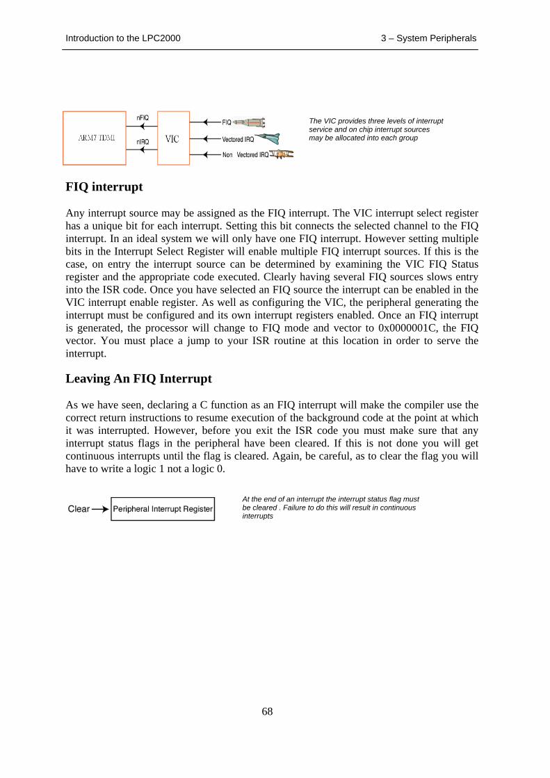
Introduction to the LPC2000 3 – System Peripherals
68
FIQ interrupt Any interrupt source may be assigned as the FIQ interrupt. The VIC interrupt select register has a unique bit for each interrupt. Setting this bit connects the selected channel to the FIQ interrupt. In an ideal system we will only have one FIQ interrupt. However setting multiple bits in the Interrupt Select Register will enable multiple FIQ interrupt sources. If this is the case, on entry the interrupt source can be determined by examining the VIC FIQ Status register and the appropriate code executed. Clearly having several FIQ sources slows entry into the ISR code. Once you have selected an FIQ source the interrupt can be enabled in the VIC interrupt enable register. As well as configuring the VIC, the peripheral generating the interrupt must be configured and its own interrupt registers enabled. Once an FIQ interrupt is generated, the processor will change to FIQ mode and vector to 0x0000001C, the FIQ vector. You must place a jump to your ISR routine at this location in order to serve the interrupt. Leaving An FIQ Interrupt As we have seen, declaring a C function as an FIQ interrupt will make the compiler use the correct return instructions to resume execution of the background code at the point at which it was interrupted. However, before you exit the ISR code you must make sure that any interrupt status flags in the peripheral have been cleared. If this is not done you will get continuous interrupts until the flag is cleared. Again, be careful, as to clear the flag you will have to write a logic 1 not a logic 0.
The VIC provides three levels of interrupt service and on chip interrupt sources may be allocated into each group
At the end of an interrupt the interrupt status flag must be cleared . Failure to do this will result in continuous interrupts
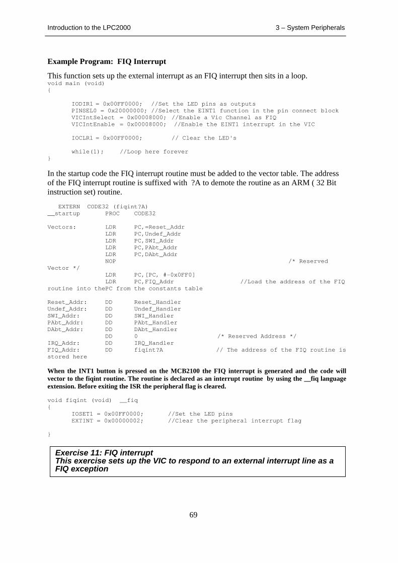
Introduction to the LPC2000 3 – System Peripherals
69
Example Program: FIQ Interrupt This function sets up the external interrupt as an FIQ interrupt then sits in a loop. void main (void) {
IODIR1 = 0x00FF0000; //Set the LED pins as outputs PINSEL0 = 0x20000000; //Select the EINT1 function in the pin connect block VICIntSelect = 0x00008000; //Enable a Vic Channel as FIQ VICIntEnable = 0x00008000; //Enable the EINT1 interrupt in the VIC
IOCLR1 = 0x00FF0000; // Clear the LED's
while(1); //Loop here forever
}
In the startup code the FIQ interrupt routine must be added to the vector table. The address of the FIQ interrupt routine is suffixed with ?A to demote the routine as an ARM ( 32 Bit instruction set) routine. EXTERN CODE32 (fiqint?A) __startup PROC CODE32 Vectors: LDR PC,=Reset_Addr LDR PC,Undef_Addr LDR PC,SWI_Addr LDR PC,PAbt_Addr LDR PC,DAbt_Addr NOP /* Reserved Vector */ LDR PC,[PC, #-0x0FF0] LDR PC,FIQ_Addr //Load the address of the FIQ routine into thePC from the constants table Reset_Addr: DD Reset_Handler Undef_Addr: DD Undef_Handler SWI_Addr: DD SWI_Handler PAbt_Addr: DD PAbt_Handler DAbt_Addr: DD DAbt_Handler DD 0 /* Reserved Address */ IRQ_Addr: DD IRQ_Handler FIQ_Addr: DD fiqint?A // The address of the FIQ routine is stored here When the INT1 button is pressed on the MCB2100 the FIQ interrupt is generated and the code will vector to the fiqint routine. The routine is declared as an interrupt routine by using the __fiq language extension. Before exiting the ISR the peripheral flag is cleared. void fiqint (void) __fiq {
IOSET1 = 0x00FF0000; //Set the LED pins EXTINT = 0x00000002; //Clear the peripheral interrupt flag
}
Exercise 11: FIQ interrupt This exercise sets up the VIC to respond to an external interrupt line as a FIQ exception
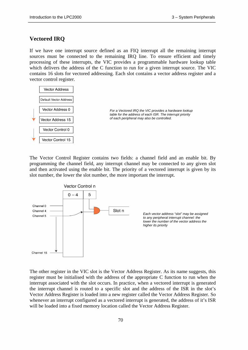
Introduction to the LPC2000 3 – System Peripherals
70
Vectored IRQ If we have one interrupt source defined as an FIQ interrupt all the remaining interrupt sources must be connected to the remaining IRQ line. To ensure efficient and timely processing of these interrupts, the VIC provides a programmable hardware lookup table which delivers the address of the C function to run for a given interrupt source. The VIC contains 16 slots for vectored addressing. Each slot contains a vector address register and a vector control register.
The Vector Control Register contains two fields: a channel field and an enable bit. By programming the channel field, any interrupt channel may be connected to any given slot and then activated using the enable bit. The priority of a vectored interrupt is given by its slot number, the lower the slot number, the more important the interrupt.
The other register in the VIC slot is the Vector Address Register. As its name suggests, this register must be initialised with the address of the appropriate C function to run when the interrupt associated with the slot occurs. In practice, when a vectored interrupt is generated the interrupt channel is routed to a specific slot and the address of the ISR in the slot’s Vector Address Register is loaded into a new register called the Vector Address Register. So whenever an interrupt configured as a vectored interrupt is generated, the address of it’s ISR will be loaded into a fixed memory location called the Vector Address Register.
For a Vectored IRQ the VIC provides a hardware lookup table for the address of each ISR. The interrupt priority of each peripheral may also be controlled.
Each vector address “slot” may be assigned to any peripheral interrupt channel: the lower the number of the vector address the higher its priority
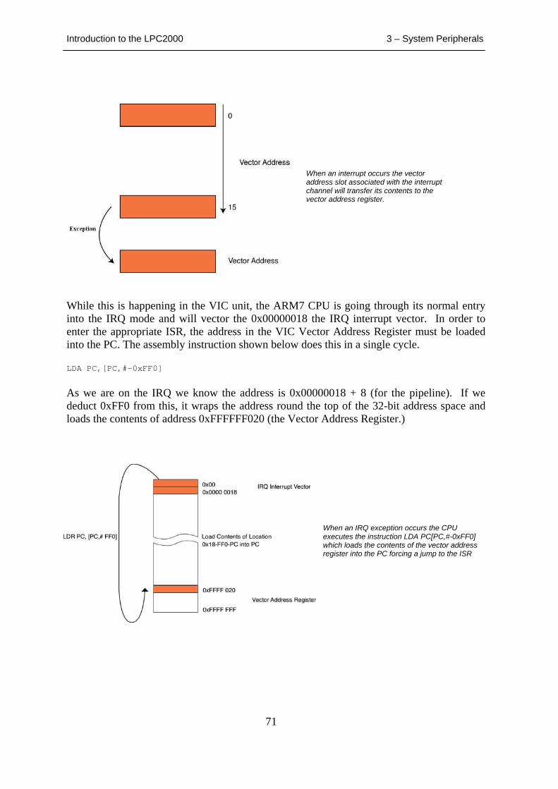
Introduction to the LPC2000 3 – System Peripherals
71
While this is happening in the VIC unit, the ARM7 CPU is going through its normal entry into the IRQ mode and will vector the 0x00000018 the IRQ interrupt vector. In order to enter the appropriate ISR, the address in the VIC Vector Address Register must be loaded into the PC. The assembly instruction shown below does this in a single cycle. LDA PC,[PC,#-0xFF0]
As we are on the IRQ we know the address is 0x00000018 + 8 (for the pipeline). If we deduct 0xFF0 from this, it wraps the address round the top of the 32-bit address space and loads the contents of address 0xFFFFFF020 (the Vector Address Register.)
When an IRQ exception occurs the CPU executes the instruction LDA PC[PC,#-0xFF0] which loads the contents of the vector address register into the PC forcing a jump to the ISR
When an interrupt occurs the vector address slot associated with the interrupt channel will transfer its contents to the vector address register.
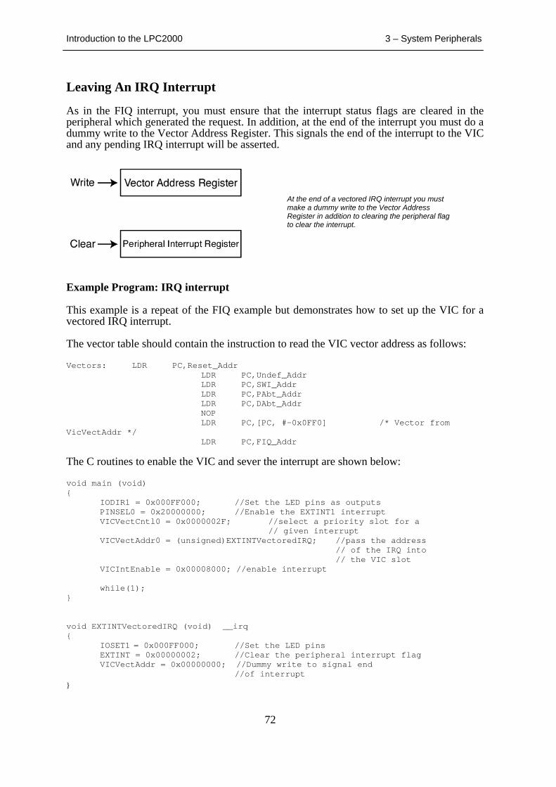
Introduction to the LPC2000 3 – System Peripherals
72
Leaving An IRQ Interrupt As in the FIQ interrupt, you must ensure that the interrupt status flags are cleared in the peripheral which generated the request. In addition, at the end of the interrupt you must do a dummy write to the Vector Address Register. This signals the end of the interrupt to the VIC and any pending IRQ interrupt will be asserted.
Example Program: IRQ interrupt This example is a repeat of the FIQ example but demonstrates how to set up the VIC for a vectored IRQ interrupt. The vector table should contain the instruction to read the VIC vector address as follows: Vectors: LDR PC,Reset_Addr LDR PC,Undef_Addr LDR PC,SWI_Addr LDR PC,PAbt_Addr LDR PC,DAbt_Addr NOP LDR PC,[PC, #-0x0FF0] /* Vector from VicVectAddr */ LDR PC,FIQ_Addr The C routines to enable the VIC and sever the interrupt are shown below: void main (void) {
IODIR1 = 0x000FF000; //Set the LED pins as outputs PINSEL0 = 0x20000000; //Enable the EXTINT1 interrupt VICVectCntl0 = 0x0000002F; //select a priority slot for a
// given interrupt VICVectAddr0 = (unsigned)EXTINTVectoredIRQ; //pass the address
// of the IRQ into // the VIC slot
VICIntEnable = 0x00008000; //enable interrupt
while(1); } void EXTINTVectoredIRQ (void) __irq {
IOSET1 = 0x000FF000; //Set the LED pins EXTINT = 0x00000002; //Clear the peripheral interrupt flag VICVectAddr = 0x00000000; //Dummy write to signal end
//of interrupt }
At the end of a vectored IRQ interrupt you must make a dummy write to the Vector Address Register in addition to clearing the peripheral flag to clear the interrupt.
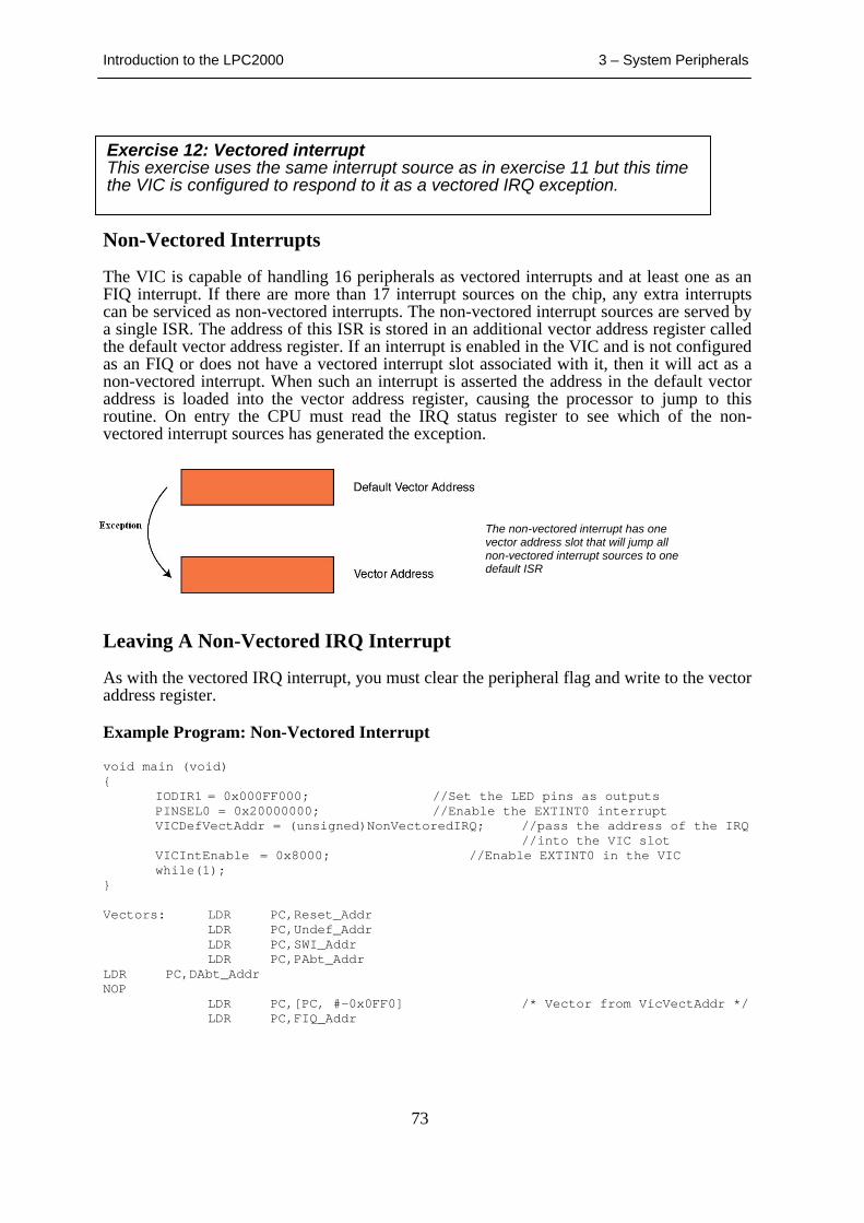
Introduction to the LPC2000 3 – System Peripherals
73
Non-Vectored Interrupts The VIC is capable of handling 16 peripherals as vectored interrupts and at least one as an FIQ interrupt. If there are more than 17 interrupt sources on the chip, any extra interrupts can be serviced as non-vectored interrupts. The non-vectored interrupt sources are served by a single ISR. The address of this ISR is stored in an additional vector address register called the default vector address register. If an interrupt is enabled in the VIC and is not configured as an FIQ or does not have a vectored interrupt slot associated with it, then it will act as a non-vectored interrupt. When such an interrupt is asserted the address in the default vector address is loaded into the vector address register, causing the processor to jump to this routine. On entry the CPU must read the IRQ status register to see which of the non-vectored interrupt sources has generated the exception.
Leaving A Non-Vectored IRQ Interrupt As with the vectored IRQ interrupt, you must clear the peripheral flag and write to the vector address register. Example Program: Non-Vectored Interrupt void main (void) {
IODIR1 = 0x000FF000; //Set the LED pins as outputs PINSEL0 = 0x20000000; //Enable the EXTINT0 interrupt VICDefVectAddr = (unsigned)NonVectoredIRQ; //pass the address of the IRQ
//into the VIC slot VICIntEnable = 0x8000; //Enable EXTINT0 in the VIC while(1);
} Vectors: LDR PC,Reset_Addr LDR PC,Undef_Addr LDR PC,SWI_Addr LDR PC,PAbt_Addr LDR PC,DAbt_Addr NOP LDR PC,[PC, #-0x0FF0] /* Vector from VicVectAddr */ LDR PC,FIQ_Addr
The non-vectored interrupt has one vector address slot that will jump all non-vectored interrupt sources to one default ISR
Exercise 12: Vectored interruptThis exercise uses the same interrupt source as in exercise 11 but this time the VIC is configured to respond to it as a vectored IRQ exception.
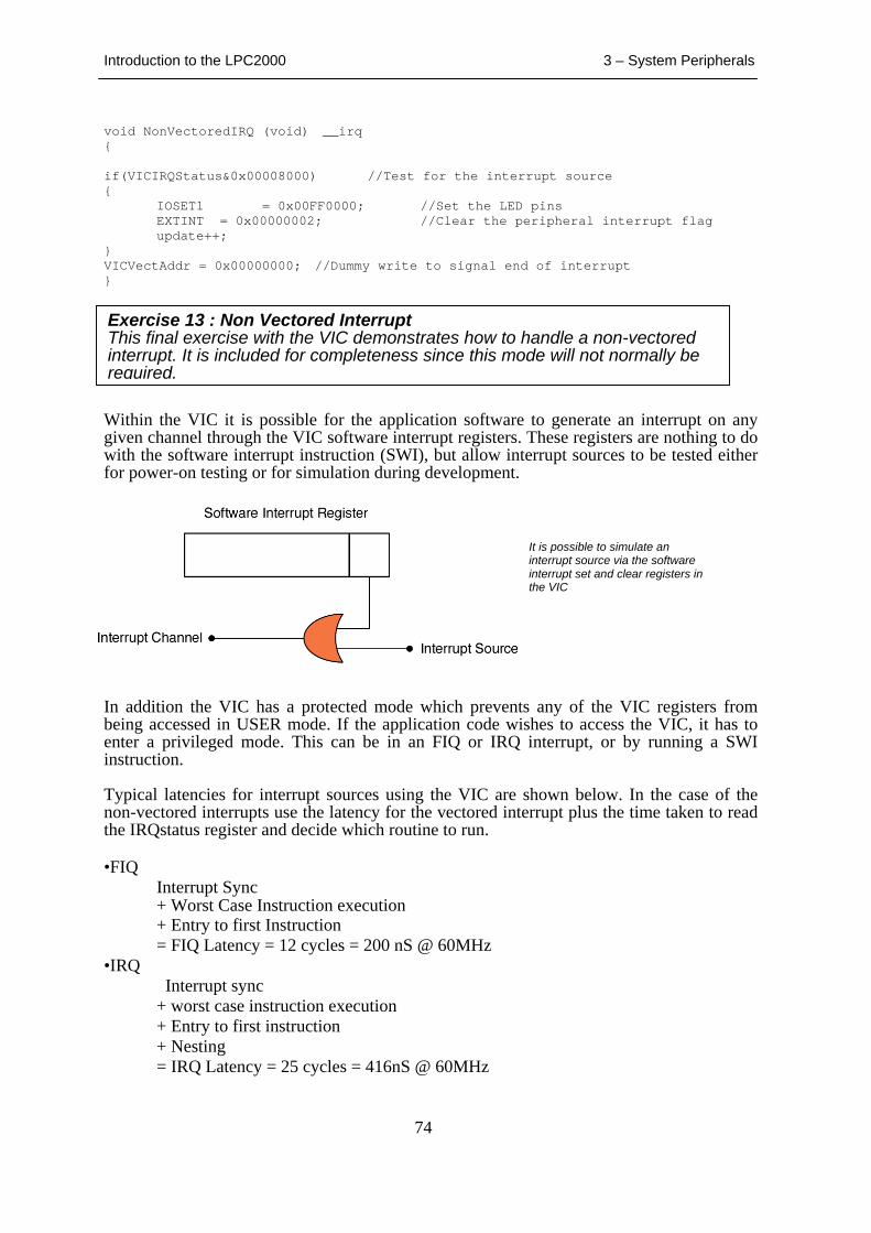
Introduction to the LPC2000 3 – System Peripherals
74
void NonVectoredIRQ (void) __irq { if(VICIRQStatus&0x00008000) //Test for the interrupt source { IOSET1 = 0x00FF0000; //Set the LED pins EXTINT = 0x00000002; //Clear the peripheral interrupt flag update++; } VICVectAddr = 0x00000000; //Dummy write to signal end of interrupt } Within the VIC it is possible for the application software to generate an interrupt on any given channel through the VIC software interrupt registers. These registers are nothing to do with the software interrupt instruction (SWI), but allow interrupt sources to be tested either for power-on testing or for simulation during development.
In addition the VIC has a protected mode which prevents any of the VIC registers from being accessed in USER mode. If the application code wishes to access the VIC, it has to enter a privileged mode. This can be in an FIQ or IRQ interrupt, or by running a SWI instruction. Typical latencies for interrupt sources using the VIC are shown below. In the case of the non-vectored interrupts use the latency for the vectored interrupt plus the time taken to read the IRQstatus register and decide which routine to run. •FIQ Interrupt Sync
+ Worst Case Instruction execution + Entry to first Instruction = FIQ Latency = 12 cycles = 200 nS @ 60MHz
•IRQ Interrupt sync + worst case instruction execution + Entry to first instruction + Nesting = IRQ Latency = 25 cycles = 416nS @ 60MHz
It is possible to simulate an interrupt source via the software interrupt set and clear registers in the VIC
Exercise 13 : Non Vectored InterruptThis final exercise with the VIC demonstrates how to handle a non-vectored interrupt. It is included for completeness since this mode will not normally be required.
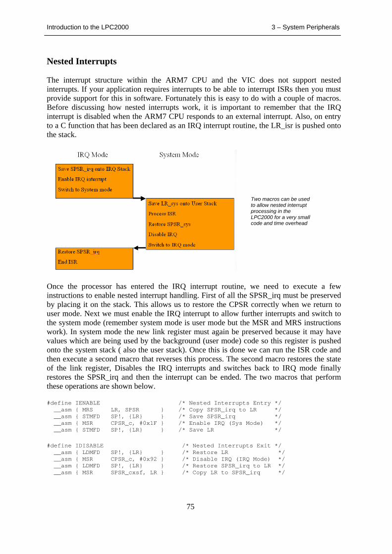
Introduction to the LPC2000 3 – System Peripherals
75
Nested Interrupts The interrupt structure within the ARM7 CPU and the VIC does not support nested interrupts. If your application requires interrupts to be able to interrupt ISRs then you must provide support for this in software. Fortunately this is easy to do with a couple of macros. Before discussing how nested interrupts work, it is important to remember that the IRQ interrupt is disabled when the ARM7 CPU responds to an external interrupt. Also, on entry to a C function that has been declared as an IRQ interrupt routine, the LR_isr is pushed onto the stack.
Once the processor has entered the IRQ interrupt routine, we need to execute a few instructions to enable nested interrupt handling. First of all the SPSR_irq must be preserved by placing it on the stack. This allows us to restore the CPSR correctly when we return to user mode. Next we must enable the IRQ interrupt to allow further interrupts and switch to the system mode (remember system mode is user mode but the MSR and MRS instructions work). In system mode the new link register must again be preserved because it may have values which are being used by the background (user mode) code so this register is pushed onto the system stack ( also the user stack). Once this is done we can run the ISR code and then execute a second macro that reverses this process. The second macro restores the state of the link register, Disables the IRQ interrupts and switches back to IRQ mode finally restores the SPSR_irq and then the interrupt can be ended. The two macros that perform these operations are shown below. #define IENABLE /* Nested Interrupts Entry */ __asm { MRS LR, SPSR } /* Copy SPSR_irq to LR */ __asm { STMFD SP!, {LR} } /* Save SPSR_irq */ __asm { MSR CPSR_c, #0x1F } /* Enable IRQ (Sys Mode) */ __asm { STMFD SP!, {LR} } /* Save LR */
#define IDISABLE /* Nested Interrupts Exit */ __asm { LDMFD SP!, {LR} } /* Restore LR */ __asm { MSR CPSR_c, #0x92 } /* Disable IRQ (IRQ Mode) */ __asm { LDMFD SP!, {LR} } /* Restore SPSR_irq to LR */ __asm { MSR SPSR_cxsf, LR } /* Copy LR to SPSR_irq */
Two macros can be used to allow nested interrupt processing in the LPC2000 for a very small code and time overhead
Introduction to the LPC2000 3 – System Peripherals
76
The total code overhead is 8 instructions or 32 Bytes for ARM code and execution of both macros takes a total of 230 nSec. This scheme allows any interrupt to interrupt any other interrupt. If you need to prioritise interrupt nesting then the macros would need to block low priority interrupts by disabling the lower priority interrupt sources in the VIC. Summary This is the most important chapter in this book as it describes the system architecture of the LPC2000 family. You must be familiar with all the topics in this chapter in order to be able to successfully configure the LPC2000 for its best performance and to avoid many of the common pitfalls which trap people new to this family of devices.
Exercise 14: Nested InterruptsOK, one last interrupt exercise. This exercise demonstrates setting a timer to generate a regular periodic interrupt which must run. It also configures an interrupt which is triggered by Eint1. The external interrupt uses the above technique to allow the timer interrupt to run even if the external interrupt routine is active.

Introduction to the LPC2000 4 – User Peripherals
77
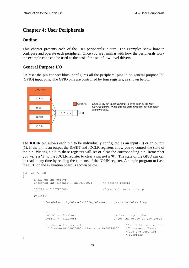
Introduction to the LPC2000 4 – User Peripherals
78
Chapter 4: User Peripherals Outline This chapter presents each of the user peripherals in turn. The examples show how to configure and operate each peripheral. Once you are familiar with how the peripherals work the example code can be used as the basis for a set of low-level drivers. General Purpose I/O
On reset the pin connect block configures all the peripheral pins to be general purpose I/O (GPIO) input pins. The GPIO pins are controlled by four registers, as shown below.
The IODIR pin allows each pin to be individually configured as an input (0) or an output (1). If the pin is an output the IOSET and IOCLR registers allow you to control the state of the pin. Writing a ‘1’ to these registers will set or clear the corresponding pin. Remember you write a ‘1’ to the IOCLR register to clear a pin not a ‘0’. The state of the GPIO pin can be read at any time by reading the contents of the IOPIN register. A simple program to flash the LED on the evaluation board is shown below. int main(void) {
unsigned int delay; unsigned int flasher = 0x00010000; // define locals
IODIR1 = 0x00FF0000; // set all ports to output
while(1) {
for(delay = 0;delay<0x10000;delay++) //simple delay loop {
; } IOCLR1 = ~flasher; //clear output pins IOSET1 = flasher; //set the state of the ports
flasher = flasher <<1; //shift the active led if(flasher&0x01000000) flasher = 0x00010000; //Increment flasher
//led and test for } //overflow
}
Each GPIO pin is controlled by a bit in each of the four GPIO registers. These bits are data direction, set and clear and pin status.
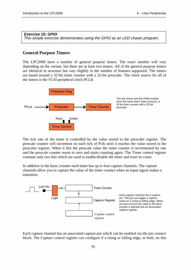
Introduction to the LPC2000 4 – User Peripherals
79
General Purpose Timers The LPC2000 have a number of general purpose timers. The exact number will vary depending on the variant, but there are at least two timers. All of the general purpose timers are identical in structure but vary slightly in the number of features supported. The timers are based around a 32-bit timer counter with a 32-bit prescaler. The clock source for all of the timers is the VLSI peripheral clock PCLK
The tick rate of the timer is controlled by the value stored in the prescaler register. The prescale counter will increment on each tick of Pclk until it reaches the value stored in the prescaler register. When it hits the prescale value the timer counter is incremented by one and the prescale counter resets to zero and starts counting again. The Timer control register contains only two bits which are used to enable/disable the timer and reset its count. In addition to the basic counter each timer has up to four capture channels. The capture channels allow you to capture the value of the timer counter when an input signal makes a transition.
Each capture channel has an associated capture pin which can be enabled via the pin connect block. The Capture control register can configure if a rising or falling edge, or both, on this
The two timers and the PWM module have the same basic timer structure. A 32-bit timer counter with a 32-bit prescaler
Each capture channel has a capture pin. This pin can trigger a capture event on a rising or falling edge. When an event occurs the value in the timer counter is latched into an associated capture register
Exercise 15: GPIOThis simple exercise demonstrates using the GPIO as an LED chaser program.
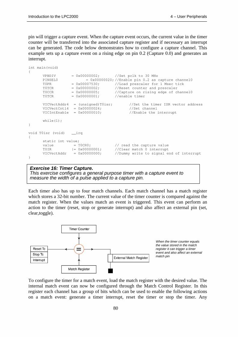
Introduction to the LPC2000 4 – User Peripherals
80
pin will trigger a capture event. When the capture event occurs, the current value in the timer counter will be transferred into the associated capture register and if necessary an interrupt can be generated. The code below demonstrates how to configure a capture channel. This example sets up a capture event on a rising edge on pin 0.2 (Capture 0.0) and generates an interrupt. int main(void) {
VPBDIV = 0x00000002; //Set pclk to 30 MHz PINSEL0 = 0x00000020; //Enable pin 0.2 as capture channel0 T0PR = 0x00007530; //Load prescaler for 1 Msec tick T0TCR = 0x00000002; //Reset counter and prescaler T0CCR = 0x00000005; //Capture on rising edge of channel0 T0TCR = 0x00000001; //enable timer
VICVectAddr4 = (unsigned)T0isr; //Set the timer ISR vector address VICVectCntl4 = 0x00000024; //Set channel VICIntEnable = 0x00000010; //Enable the interrupt
while(1);
} void T0isr (void) __irq {
static int value; value = T0CR0; // read the capture value T0IR |= 0x00000001; //Clear match 0 interrupt VICVectAddr = 0x00000000; //Dummy write to signal end of interrupt
}
Each timer also has up to four match channels. Each match channel has a match register which stores a 32-bit number. The current value of the timer counter is compared against the match register. When the values match an event is triggered. This event can perform an action to the timer (reset, stop or generate interrupt) and also affect an external pin (set, clear,toggle).
To configure the timer for a match event, load the match register with the desired value. The internal match event can now be configured through the Match Control Register. In this register each channel has a group of bits which can be used to enable the following actions on a match event: generate a timer interrupt, reset the timer or stop the timer. Any
When the timer counter equals the value stored in the match register it can trigger a timer event and also affect an external match pin
Exercise 16: Timer Capture. This exercise configures a general purpose timer with a capture event to measure the width of a pulse applied to a capture pin.
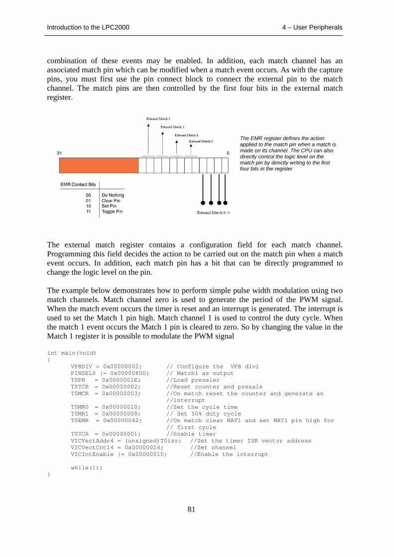
Introduction to the LPC2000 4 – User Peripherals
81
combination of these events may be enabled. In addition, each match channel has an associated match pin which can be modified when a match event occurs. As with the capture pins, you must first use the pin connect block to connect the external pin to the match channel. The match pins are then controlled by the first four bits in the external match register.
The external match register contains a configuration field for each match channel. Programming this field decides the action to be carried out on the match pin when a match event occurs. In addition, each match pin has a bit that can be directly programmed to change the logic level on the pin. The example below demonstrates how to perform simple pulse width modulation using two match channels. Match channel zero is used to generate the period of the PWM signal. When the match event occurs the timer is reset and an interrupt is generated. The interrupt is used to set the Match 1 pin high. Match channel 1 is used to control the duty cycle. When the match 1 event occurs the Match 1 pin is cleared to zero. So by changing the value in the Match 1 register it is possible to modulate the PWM signal int main(void) {
VPBDIV = 0x00000002; // Configure the VPB divi PINSEL0 |= 0x00000800; // Match1 as output T0PR = 0x0000001E; //Load presaler T0TCR = 0x00000002; //Reset counter and presale T0MCR = 0x00000003; //On match reset the counter and generate an
//interrupt T0MR0 = 0x00000010; //Set the cycle time T0MR1 = 0x00000008; // Set 50% duty cycle T0EMR = 0x00000042; //On match clear MAT1 and set MAT1 pin high for
// first cycle T0TCR = 0x00000001; //Enable timer VICVectAddr4 = (unsigned)T0isr; //Set the timer ISR vector address VICVectCntl4 = 0x00000024; //Set channel VICIntEnable |= 0x00000010; //Enable the interrupt
while(1);
}
The EMR register defines the action applied to the match pin when a match is made on its channel. The CPU can also directly control the logic level on the match pin by directly writing to the first four bits in the register
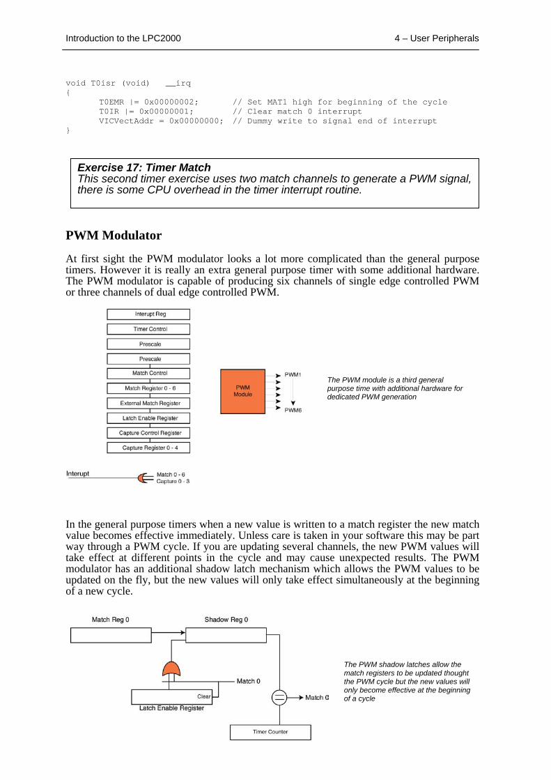
Introduction to the LPC2000 4 – User Peripherals
82
void T0isr (void) __irq {
T0EMR |= 0x00000002; // Set MAT1 high for beginning of the cycle T0IR |= 0x00000001; // Clear match 0 interrupt VICVectAddr = 0x00000000; // Dummy write to signal end of interrupt
}
PWM Modulator At first sight the PWM modulator looks a lot more complicated than the general purpose timers. However it is really an extra general purpose timer with some additional hardware. The PWM modulator is capable of producing six channels of single edge controlled PWM or three channels of dual edge controlled PWM.
In the general purpose timers when a new value is written to a match register the new match value becomes effective immediately. Unless care is taken in your software this may be part way through a PWM cycle. If you are updating several channels, the new PWM values will take effect at different points in the cycle and may cause unexpected results. The PWM modulator has an additional shadow latch mechanism which allows the PWM values to be updated on the fly, but the new values will only take effect simultaneously at the beginning of a new cycle.
The PWM module is a third general purpose time with additional hardware for dedicated PWM generation
The PWM shadow latches allow the match registers to be updated thought the PWM cycle but the new values will only become effective at the beginning of a cycle
Exercise 17: Timer Match This second timer exercise uses two match channels to generate a PWM signal, there is some CPU overhead in the timer interrupt routine.
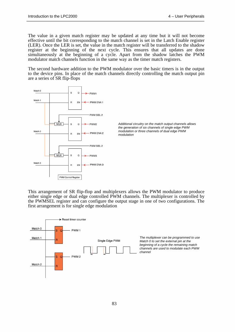
Introduction to the LPC2000 4 – User Peripherals
83
The value in a given match register may be updated at any time but it will not become effective until the bit corresponding to the match channel is set in the Latch Enable register (LER). Once the LER is set, the value in the match register will be transferred to the shadow register at the beginning of the next cycle. This ensures that all updates are done simultaneously at the beginning of a cycle. Apart from the shadow latches the PWM modulator match channels function in the same way as the timer match registers. The second hardware addition to the PWM modulator over the basic timers is in the output to the device pins. In place of the match channels directly controlling the match output pin are a series of SR flip-flops
This arrangement of SR flip-flop and multiplexers allows the PWM modulator to produce either single edge or dual edge controlled PWM channels. The multiplexer is controlled by the PWMSEL register and can configure the output stage in one of two configurations. The first arrangement is for single edge modulation
Additional circuitry on the match output channels allows the generation of six channels of single edge PWM modulation or three channels of dual edge PWM modulation
The multiplexer can be programmed to use Match 0 to set the external pin at the beginning of a cycle the remaining match channels are used to modulate each PWM channel
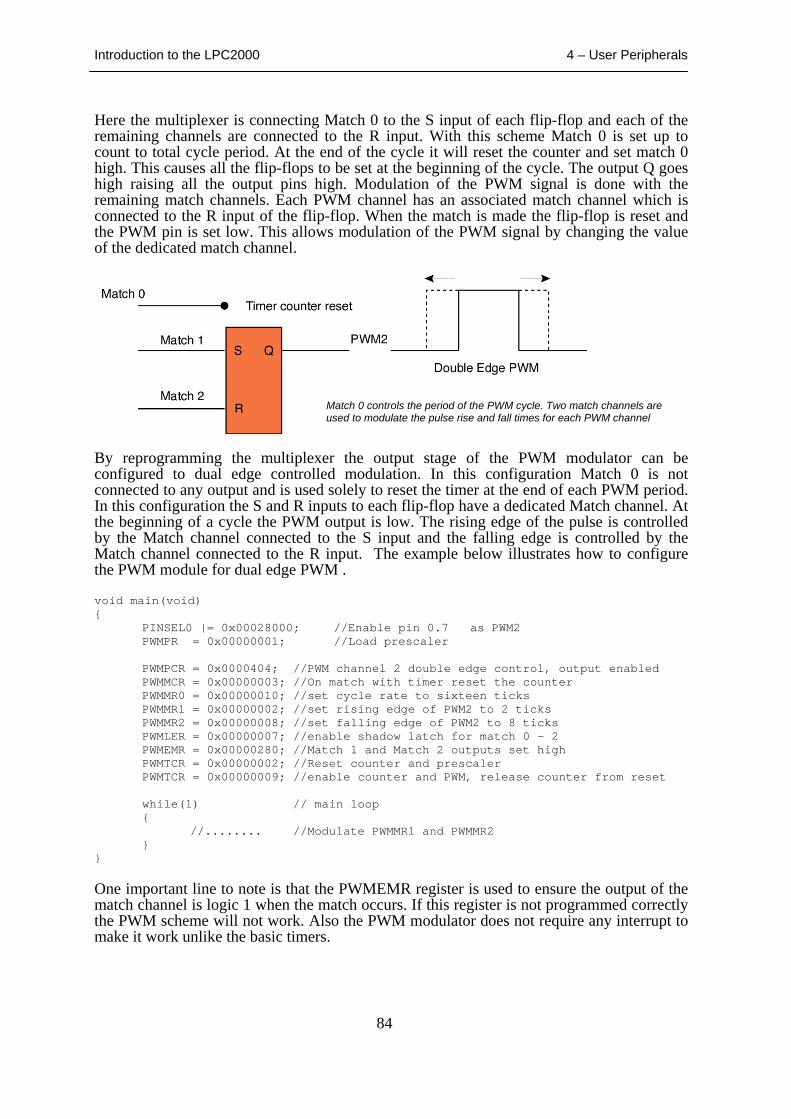
Introduction to the LPC2000 4 – User Peripherals
84
Here the multiplexer is connecting Match 0 to the S input of each flip-flop and each of the remaining channels are connected to the R input. With this scheme Match 0 is set up to count to total cycle period. At the end of the cycle it will reset the counter and set match 0 high. This causes all the flip-flops to be set at the beginning of the cycle. The output Q goes high raising all the output pins high. Modulation of the PWM signal is done with the remaining match channels. Each PWM channel has an associated match channel which is connected to the R input of the flip-flop. When the match is made the flip-flop is reset and the PWM pin is set low. This allows modulation of the PWM signal by changing the value of the dedicated match channel.
By reprogramming the multiplexer the output stage of the PWM modulator can be configured to dual edge controlled modulation. In this configuration Match 0 is not connected to any output and is used solely to reset the timer at the end of each PWM period. In this configuration the S and R inputs to each flip-flop have a dedicated Match channel. At the beginning of a cycle the PWM output is low. The rising edge of the pulse is controlled by the Match channel connected to the S input and the falling edge is controlled by the Match channel connected to the R input. The example below illustrates how to configure the PWM module for dual edge PWM . void main(void) {
PINSEL0 |= 0x00028000; //Enable pin 0.7 as PWM2 PWMPR = 0x00000001; //Load prescaler
PWMPCR = 0x0000404; //PWM channel 2 double edge control, output enabled PWMMCR = 0x00000003; //On match with timer reset the counter PWMMR0 = 0x00000010; //set cycle rate to sixteen ticks PWMMR1 = 0x00000002; //set rising edge of PWM2 to 2 ticks PWMMR2 = 0x00000008; //set falling edge of PWM2 to 8 ticks PWMLER = 0x00000007; //enable shadow latch for match 0 - 2 PWMEMR = 0x00000280; //Match 1 and Match 2 outputs set high PWMTCR = 0x00000002; //Reset counter and prescaler PWMTCR = 0x00000009; //enable counter and PWM, release counter from reset
while(1) // main loop {
//........ //Modulate PWMMR1 and PWMMR2 }
} One important line to note is that the PWMEMR register is used to ensure the output of the match channel is logic 1 when the match occurs. If this register is not programmed correctly the PWM scheme will not work. Also the PWM modulator does not require any interrupt to make it work unlike the basic timers.
Match 0 controls the period of the PWM cycle. Two match channels are used to modulate the pulse rise and fall times for each PWM channel
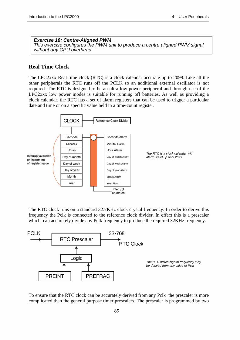
Introduction to the LPC2000 4 – User Peripherals
85
Real Time Clock The LPC2xxx Real time clock (RTC) is a clock calendar accurate up to 2099. Like all the other peripherals the RTC runs off the PCLK so an additional external oscillator is not required. The RTC is designed to be an ultra low power peripheral and through use of the LPC2xxx low power modes is suitable for running off batteries. As well as providing a clock calendar, the RTC has a set of alarm registers that can be used to trigger a particular date and time or on a specific value held in a time-count register.
The RTC clock runs on a standard 32.7KHz clock crystal frequency. In order to derive this frequency the Pclk is connected to the reference clock divider. In effect this is a prescaler whicht can accurately divide any Pclk frequency to produce the required 32KHz frequency.
To ensure that the RTC clock can be accurately derived from any Pclk the prescaler is more complicated than the general purpose timer prescalers. The prescaler is programmed by two
The RTC is a clock calendar with alarm valid up until 2099
The RTC watch crystal frequency may be derived from any value of Pclk
Exercise 18: Centre-Aligned PWMThis exercise configures the PWM unit to produce a centre aligned PWM signal without any CPU overhead.
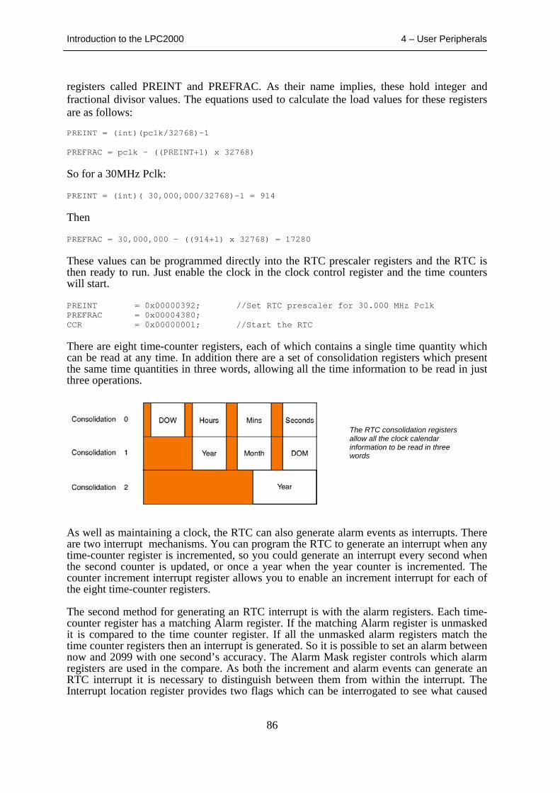
Introduction to the LPC2000 4 – User Peripherals
86
registers called PREINT and PREFRAC. As their name implies, these hold integer and fractional divisor values. The equations used to calculate the load values for these registers are as follows: PREINT = (int)(pclk/32768)-1 PREFRAC = pclk – ((PREINT+1) x 32768) So for a 30MHz Pclk: PREINT = (int)( 30,000,000/32768)-1 = 914 Then PREFRAC = 30,000,000 – ((914+1) x 32768) = 17280 These values can be programmed directly into the RTC prescaler registers and the RTC is then ready to run. Just enable the clock in the clock control register and the time counters will start. PREINT = 0x00000392; //Set RTC prescaler for 30.000 MHz Pclk PREFRAC = 0x00004380; CCR = 0x00000001; //Start the RTC There are eight time-counter registers, each of which contains a single time quantity which can be read at any time. In addition there are a set of consolidation registers which present the same time quantities in three words, allowing all the time information to be read in just three operations.
As well as maintaining a clock, the RTC can also generate alarm events as interrupts. There are two interrupt mechanisms. You can program the RTC to generate an interrupt when any time-counter register is incremented, so you could generate an interrupt every second when the second counter is updated, or once a year when the year counter is incremented. The counter increment interrupt register allows you to enable an increment interrupt for each of the eight time-counter registers. The second method for generating an RTC interrupt is with the alarm registers. Each time- counter register has a matching Alarm register. If the matching Alarm register is unmasked it is compared to the time counter register. If all the unmasked alarm registers match the time counter registers then an interrupt is generated. So it is possible to set an alarm between now and 2099 with one second’s accuracy. The Alarm Mask register controls which alarm registers are used in the compare. As both the increment and alarm events can generate an RTC interrupt it is necessary to distinguish between them from within the interrupt. The Interrupt location register provides two flags which can be interrogated to see what caused
The RTC consolidation registers allow all the clock calendar information to be read in three words
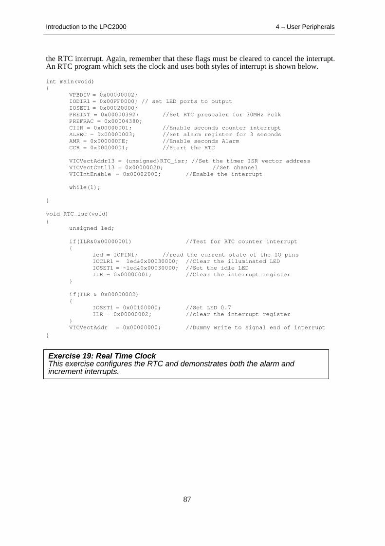
Introduction to the LPC2000 4 – User Peripherals
87
the RTC interrupt. Again, remember that these flags must be cleared to cancel the interrupt. An RTC program which sets the clock and uses both styles of interrupt is shown below. int main(void) {
VPBDIV = 0x00000002; IODIR1 = 0x00FF0000; // set LED ports to output IOSET1 = 0x00020000; PREINT = 0x00000392; //Set RTC prescaler for 30MHz Pclk PREFRAC = 0x00004380; CIIR = 0x00000001; //Enable seconds counter interrupt ALSEC = 0x00000003; //Set alarm register for 3 seconds AMR = 0x000000FE; //Enable seconds Alarm CCR = 0x00000001; //Start the RTC
VICVectAddr13 = (unsigned)RTC_isr; //Set the timer ISR vector address VICVectCntl13 = 0x0000002D; //Set channel VICIntEnable = 0x00002000; //Enable the interrupt
while(1);
} void RTC_isr(void) {
unsigned led;
if(ILR&0x00000001) //Test for RTC counter interrupt {
led = IOPIN1; //read the current state of the IO pins IOCLR1 = led&0x00030000; //Clear the illuminated LED IOSET1 = ~led&0x00030000; //Set the idle LED ILR = 0x00000001; //Clear the interrupt register
}
if(ILR & 0x00000002) {
IOSET1 = 0x00100000; //Set LED 0.7 ILR = 0x00000002; //clear the interrupt register
} VICVectAddr = 0x00000000; //Dummy write to signal end of interrupt
}
Exercise 19: Real Time Clock This exercise configures the RTC and demonstrates both the alarm and increment interrupts.
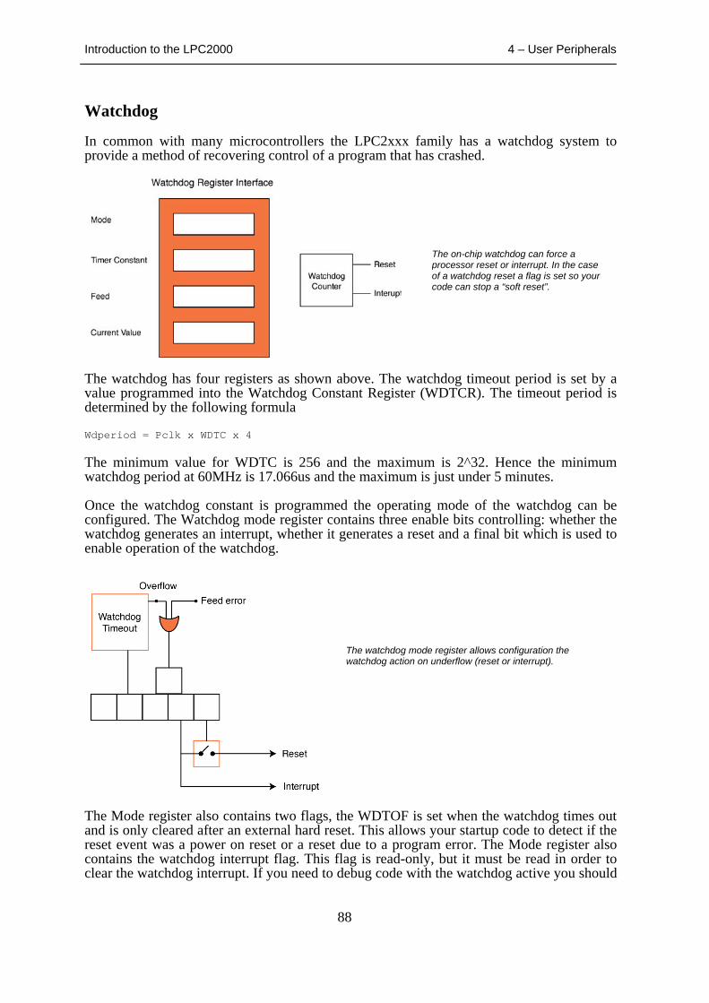
Introduction to the LPC2000 4 – User Peripherals
88
Watchdog In common with many microcontrollers the LPC2xxx family has a watchdog system to provide a method of recovering control of a program that has crashed.
The watchdog has four registers as shown above. The watchdog timeout period is set by a value programmed into the Watchdog Constant Register (WDTCR). The timeout period is determined by the following formula Wdperiod = Pclk x WDTC x 4 The minimum value for WDTC is 256 and the maximum is 2^32. Hence the minimum watchdog period at 60MHz is 17.066us and the maximum is just under 5 minutes. Once the watchdog constant is programmed the operating mode of the watchdog can be configured. The Watchdog mode register contains three enable bits controlling: whether the watchdog generates an interrupt, whether it generates a reset and a final bit which is used to enable operation of the watchdog.
The Mode register also contains two flags, the WDTOF is set when the watchdog times out and is only cleared after an external hard reset. This allows your startup code to detect if the reset event was a power on reset or a reset due to a program error. The Mode register also contains the watchdog interrupt flag. This flag is read-only, but it must be read in order to clear the watchdog interrupt. If you need to debug code with the watchdog active you should
The on-chip watchdog can force a processor reset or interrupt. In the case of a watchdog reset a flag is set so your code can stop a “soft reset”.
The watchdog mode register allows configuration the watchdog action on underflow (reset or interrupt).
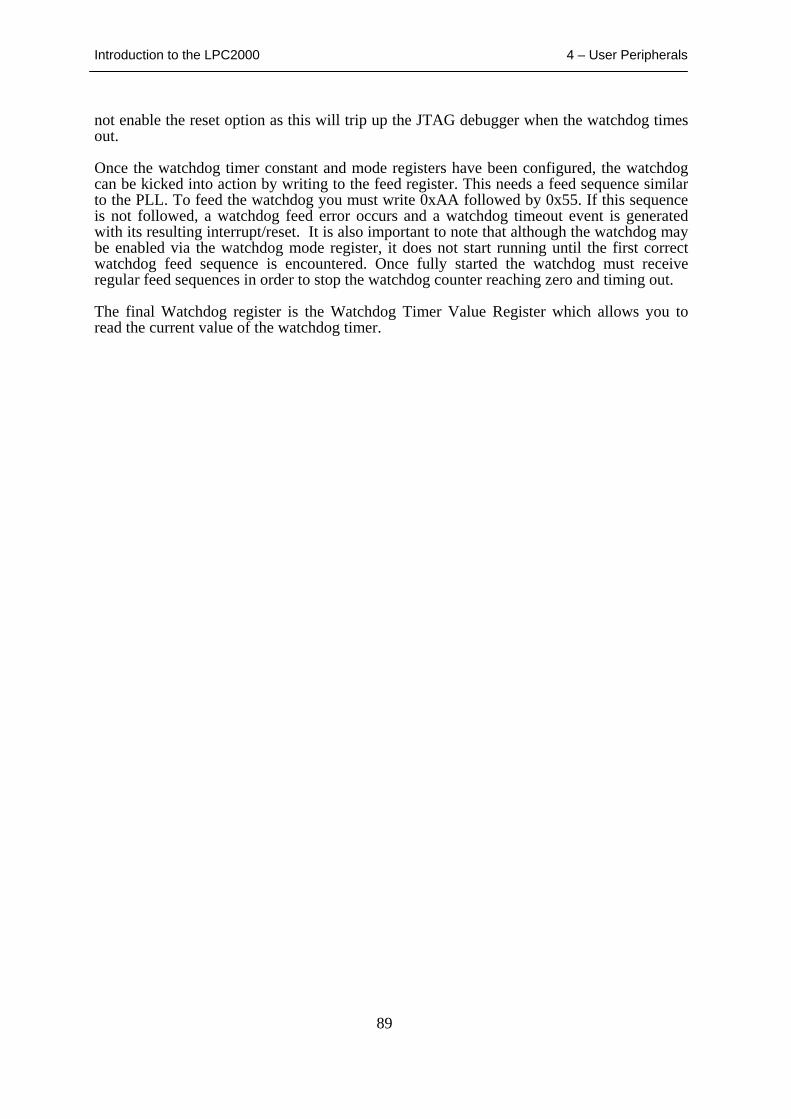
Introduction to the LPC2000 4 – User Peripherals
89
not enable the reset option as this will trip up the JTAG debugger when the watchdog times out. Once the watchdog timer constant and mode registers have been configured, the watchdog can be kicked into action by writing to the feed register. This needs a feed sequence similar to the PLL. To feed the watchdog you must write 0xAA followed by 0x55. If this sequence is not followed, a watchdog feed error occurs and a watchdog timeout event is generated with its resulting interrupt/reset. It is also important to note that although the watchdog may be enabled via the watchdog mode register, it does not start running until the first correct watchdog feed sequence is encountered. Once fully started the watchdog must receive regular feed sequences in order to stop the watchdog counter reaching zero and timing out. The final Watchdog register is the Watchdog Timer Value Register which allows you to read the current value of the watchdog timer.
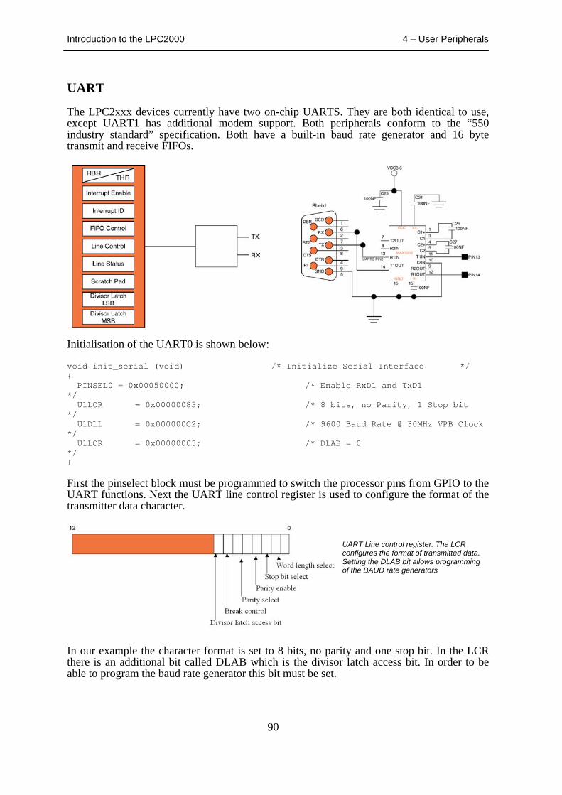
Introduction to the LPC2000 4 – User Peripherals
90
UART The LPC2xxx devices currently have two on-chip UARTS. They are both identical to use, except UART1 has additional modem support. Both peripherals conform to the “550 industry standard” specification. Both have a built-in baud rate generator and 16 byte transmit and receive FIFOs.
Initialisation of the UART0 is shown below: void init_serial (void) /* Initialize Serial Interface */ { PINSEL0 = 0x00050000; /* Enable RxD1 and TxD1 */ U1LCR = 0x00000083; /* 8 bits, no Parity, 1 Stop bit */ U1DLL = 0x000000C2; /* 9600 Baud Rate @ 30MHz VPB Clock */ U1LCR = 0x00000003; /* DLAB = 0 */ } First the pinselect block must be programmed to switch the processor pins from GPIO to the UART functions. Next the UART line control register is used to configure the format of the transmitter data character.
In our example the character format is set to 8 bits, no parity and one stop bit. In the LCR there is an additional bit called DLAB which is the divisor latch access bit. In order to be able to program the baud rate generator this bit must be set.
UART Line control register: The LCR configures the format of transmitted data. Setting the DLAB bit allows programming of the BAUD rate generators
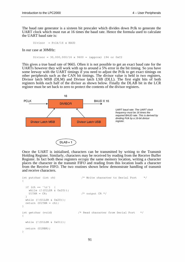
Introduction to the LPC2000 4 – User Peripherals
91
The baud rate generator is a sixteen bit prescaler which divides down Pclk to generate the UART clock which must run at 16 times the baud rate. Hence the formula used to calculate the UART baud rate is: Divisor = Pclk/16 x BAUD In our case at 30MHz: Divisor = 30,000,000/16 x 9600 = (approx) 194 or 0xC2 This gives a true baud rate of 9665. Often it is not possible to get an exact baud rate for the UARTs however they will work with up to around a 5% error in the bit timing. So you have some leeway with the UART timings if you need to adjust the Pclk to get exact timings on other peripherals such as the CAN bit timings. The divisor value is held in two registers, Divisor latch MSB (DLM) and Divisor latch LSB (DLL). The first eight bits of both registers holds each half of the divisor as shown below. Finally the DLAB bit in the LCR register must be set back to zero to protect the contents of the divisor registers.
Once the UART is initialised, characters can be transmitted by writing to the Transmit Holding Register. Similarly, characters may be received by reading from the Receive Buffer Register. In fact both these registers occupy the same memory location, writing a character places the character in the transmit FIFO and reading from this location loads a character from the Receive FIFO. The two routines shown below demonstrate handling of transmit and receive characters. int putchar (int ch) /* Write character to Serial Port */ { if (ch == '\n') { while (!(U1LSR & 0x20)); U1THR = CR; /* output CR */ } while (!(U1LSR & 0x20)); return (U1THR = ch); } int getchar (void) /* Read character from Serial Port */ { while (!(U1LSR & 0x01)); return (U1RBR); }
UART baud rate: The UART clock frequency must be 16 times the required BAUD rate. This is derived by dividing Pclk by a 16-bit divisor register.
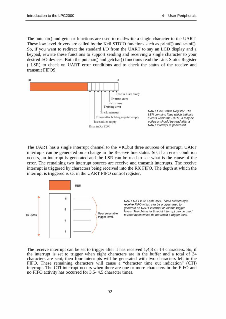
Introduction to the LPC2000 4 – User Peripherals
92
The putchar() and getchar functions are used to read/write a single character to the UART. These low level drivers are called by the Keil STDIO functions such as printf() and scanf(). So, if you want to redirect the standard I/O from the UART to say an LCD display and a keypad, rewrite these functions to support sending and receiving a single character to your desired I/O devices. Both the putchar() and getchar() functions read the Link Status Register ( LSR) to check on UART error conditions and to check the status of the receive and transmit FIFOS.
The UART has a single interrupt channel to the VIC,but three sources of interrupt. UART interrupts can be generated on a change in the Receive line status. So, if an error condition occurs, an interrupt is generated and the LSR can be read to see what is the cause of the error. The remaining two interrupt sources are receive and transmit interrupts. The receive interrupt is triggered by characters being received into the RX FIFO. The depth at which the interrupt is triggered is set in the UART FIFO control register.
The receive interrupt can be set to trigger after it has received 1,4,8 or 14 characters. So, if the interrupt is set to trigger when eight characters are in the buffer and a total of 34 characters are sent, then four interrupts will be generated with two characters left in the FIFO. These remaining characters will cause a “character time out indication” (CTI) interrupt. The CTI interrupt occurs when there are one or more characters in the FIFO and no FIFO activity has occurred for 3.5- 4.5 character times.
UART Line Status Register: The LSR contains flags which indicate events within the UART. It may be polled or should be read after a UART interrupt is generated.
UART RX FIFO: Each UART has a sixteen byte receive FIFO which can be programmed to generate an UART interrupt at various trigger levels. The character timeout interrupt can be used to read bytes which do not reach a trigger level.
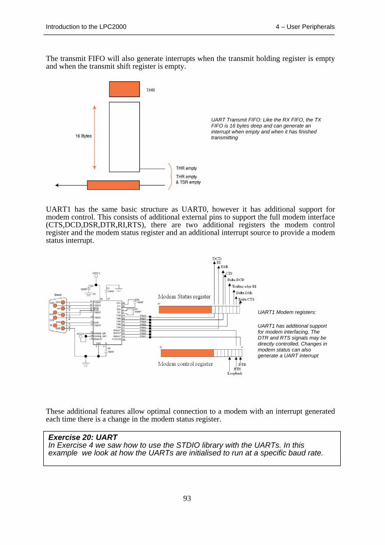
Introduction to the LPC2000 4 – User Peripherals
93
The transmit FIFO will also generate interrupts when the transmit holding register is empty and when the transmit shift register is empty.
UART1 has the same basic structure as UART0, however it has additional support for modem control. This consists of additional external pins to support the full modem interface (CTS,DCD,DSR,DTR,RI,RTS), there are two additional registers the modem control register and the modem status register and an additional interrupt source to provide a modem status interrupt.
These additional features allow optimal connection to a modem with an interrupt generated each time there is a change in the modem status register.
UART Transmit FIFO: Like the RX FIFO, the TX FIFO is 16 bytes deep and can generate an interrupt when empty and when it has finished transmitting
UART1 Modem registers:
UART1 has additional support for modem interfacing. The DTR and RTS signals may be directly controlled. Changes in modem status can also generate a UART interrupt
Exercise 20: UARTIn Exercise 4 we saw how to use the STDIO library with the UARTs. In this example we look at how the UARTs are initialised to run at a specific baud rate.
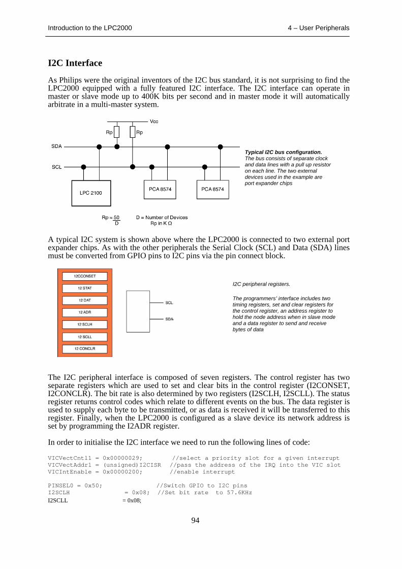
Introduction to the LPC2000 4 – User Peripherals
94
I2C Interface As Philips were the original inventors of the I2C bus standard, it is not surprising to find the LPC2000 equipped with a fully featured I2C interface. The I2C interface can operate in master or slave mode up to 400K bits per second and in master mode it will automatically arbitrate in a multi-master system.
A typical I2C system is shown above where the LPC2000 is connected to two external port expander chips. As with the other peripherals the Serial Clock (SCL) and Data (SDA) lines must be converted from GPIO pins to I2C pins via the pin connect block.
The I2C peripheral interface is composed of seven registers. The control register has two separate registers which are used to set and clear bits in the control register (I2CONSET, I2CONCLR). The bit rate is also determined by two registers (I2SCLH, I2SCLL). The status register returns control codes which relate to different events on the bus. The data register is used to supply each byte to be transmitted, or as data is received it will be transferred to this register. Finally, when the LPC2000 is configured as a slave device its network address is set by programming the I2ADR register. In order to initialise the I2C interface we need to run the following lines of code: VICVectCntl1 = 0x00000029; //select a priority slot for a given interrupt VICVectAddr1 = (unsigned)I2CISR //pass the address of the IRQ into the VIC slot VICIntEnable = 0x00000200; //enable interrupt PINSEL0 = 0x50; //Switch GPIO to I2C pins I2SCLH = 0x08; //Set bit rate to 57.6KHz I2SCLL = 0x08;
I2C peripheral registers.
The programmers’ interface includes two timing registers, set and clear registers for the control register, an address register to hold the node address when in slave mode and a data register to send and receive bytes of data
Typical I2C bus configuration. The bus consists of separate clock and data lines with a pull up resistor on each line. The two external devices used in the example are port expander chips
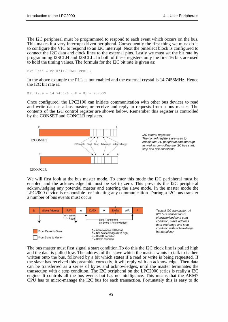
Introduction to the LPC2000 4 – User Peripherals
95
The I2C peripheral must be programmed to respond to each event which occurs on the bus. This makes it a very interrupt-driven peripheral. Consequently the first thing we must do is to configure the VIC to respond to an I2C interrupt. Next the pinselect block is configured to connect the I2C data and clock lines to the external pins. Lastly we must set the bit rate by programming I2SCLH and I2SCLL. In both of these registers only the first 16 bits are used to hold the timing values. The formula for the I2C bit rate is given as: Bit Rate = Pclk/(I2SCLH+I2CSLL) In the above example the PLL is not enabled and the external crystal is 14.7456MHz. Hence the I2C bit rate is: Bit Rate = 14.7456/B ( 8 + 8) = 937500 Once configured, the LPC2100 can initiate communication with other bus devices to read and write data as a bus master, or receive and reply to requests from a bus master. The contents of the I2C control register are shown below. Remember this register is controlled by the CONSET and CONCLR registers.
We will first look at the bus master mode. To enter this mode the I2C peripheral must be enabled and the acknowledge bit must be set to zero. This prevents the I2C peripheral acknowledging any potential master and entering the slave mode. In the master mode the LPC2000 device is responsible for initiating any communication. During a I2C bus transfer a number of bus events must occur.
The bus master must first signal a start condition.To do this the I2C clock line is pulled high and the data is pulled low. The address of the slave which the master wants to talk to is then written onto the bus, followed by a bit which states if a read or write is being requested. If the slave has received this preamble correctly, it will reply with an acknowledge. Then data can be transferred as a series of bytes and acknowledges, until the master terminates the transaction with a stop condition. The I2C peripheral on the LPC2000 series is really a I2C engine. It controls all the bus events but has no intelligence. This means that the ARM7 CPU has to micro-manage the I2C bus for each transaction. Fortunately this is easy to do
I2C control registers: The control registers are used to enable the I2C peripheral and interrupt as well as controlling the I2C bus start, stop and ack conditions.
Typical I2C transaction :A I2C bus transaction is characterised by a start condition, slave address data exchange and stop condition with acknowledge handshaking
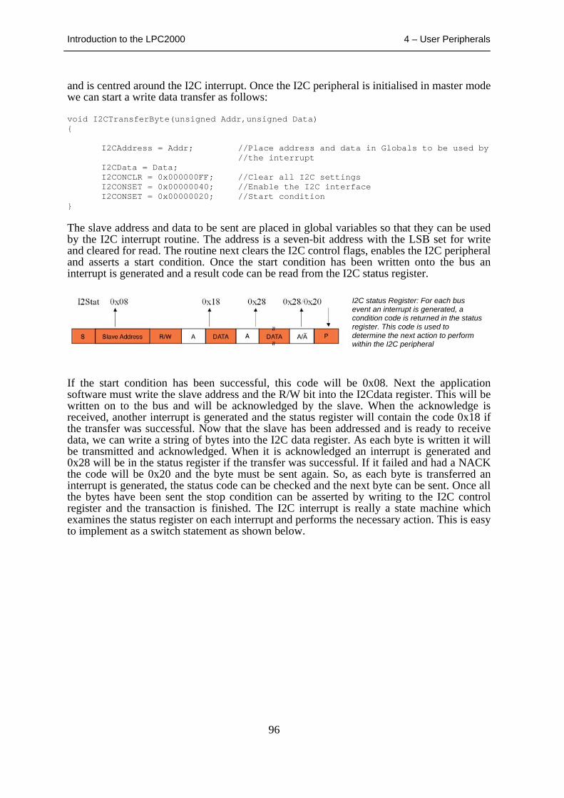
Introduction to the LPC2000 4 – User Peripherals
96
and is centred around the I2C interrupt. Once the I2C peripheral is initialised in master mode we can start a write data transfer as follows: void I2CTransferByte(unsigned Addr,unsigned Data) {
I2CAddress = Addr; //Place address and data in Globals to be used by //the interrupt
I2CData = Data; I2CONCLR = 0x000000FF; //Clear all I2C settings I2CONSET = 0x00000040; //Enable the I2C interface I2CONSET = 0x00000020; //Start condition
} The slave address and data to be sent are placed in global variables so that they can be used by the I2C interrupt routine. The address is a seven-bit address with the LSB set for write and cleared for read. The routine next clears the I2C control flags, enables the I2C peripheral and asserts a start condition. Once the start condition has been written onto the bus an interrupt is generated and a result code can be read from the I2C status register.
If the start condition has been successful, this code will be 0x08. Next the application software must write the slave address and the R/W bit into the I2Cdata register. This will be written on to the bus and will be acknowledged by the slave. When the acknowledge is received, another interrupt is generated and the status register will contain the code 0x18 if the transfer was successful. Now that the slave has been addressed and is ready to receive data, we can write a string of bytes into the I2C data register. As each byte is written it will be transmitted and acknowledged. When it is acknowledged an interrupt is generated and 0x28 will be in the status register if the transfer was successful. If it failed and had a NACK the code will be 0x20 and the byte must be sent again. So, as each byte is transferred an interrupt is generated, the status code can be checked and the next byte can be sent. Once all the bytes have been sent the stop condition can be asserted by writing to the I2C control register and the transaction is finished. The I2C interrupt is really a state machine which examines the status register on each interrupt and performs the necessary action. This is easy to implement as a switch statement as shown below.
I2C status Register: For each bus event an interrupt is generated, a condition code is returned in the status register. This code is used to determine the next action to perform within the I2C peripheral
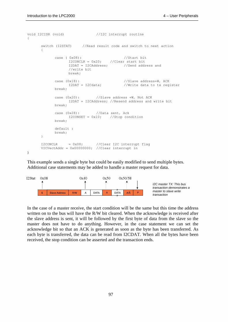
Introduction to the LPC2000 4 – User Peripherals
97
void I2CISR (void) //I2C interrupt routine {
switch (I2STAT) //Read result code and switch to next action {
case ( 0x08): //Start bit
I2CONCLR = 0x20; //Clear start bit I2DAT = I2CAddress; //Send address and //write bit break;
case (0x18): //Slave address+W, ACK
I2DAT = I2Cdata; //Write data to tx register break;
case (0x20): //Slave address +W, Not ACK
I2DAT = I2CAddress; //Resend address and write bit break;
case (0x28): //Data sent, Ack
I2CONSET = 0x10; //Stop condition break;
default : break;
}
I2CONCLR = 0x08; //Clear I2C interrupt flag VICVectAddr = 0x00000000; //Clear interrupt in
} This example sends a single byte but could be easily modified to send multiple bytes. Additional case statements may be added to handle a master request for data.
In the case of a master receive, the start condition will be the same but this time the address written on to the bus will have the R/W bit cleared. When the acknowledge is received after the slave address is sent, it will be followed by the first byte of data from the slave so the master does not have to do anything. However, in the case statement we can set the acknowledge bit so that an ACK is generated as soon as the byte has been transferred. As each byte is transferred, the data can be read from I2CDAT. When all the bytes have been received, the stop condition can be asserted and the transaction ends.
I2C master TX: This bus transaction demonstrates a master to slave write transaction
Introduction to the LPC2000 4 – User Peripherals
98
The same I2CtransferByte() function can be used to start a read transaction and the additional case statements required in the interrupt are shown below. case (0x40) : //Slave Address +R, ACK
I2CONSET = 0x04; //Enable ACK for data byte break; case (0x48) : //Slave Address +R, Not Ack
I2CONSET = 0x20; //Resend Start condition break; case (0x50) : //Data Received, ACK
message = I2DAT; I2CONSET = 0x10; //Stop condition
lock = 0; //Signal end of I2C activity break; case (0x58): //Data Received, Not Ack
I2CONSET = 0x20; // Resend Start condition break;
Exercise 21: I2C This exercise demonstrates how to use the I2C interface to communicate to an I2C EEROM.
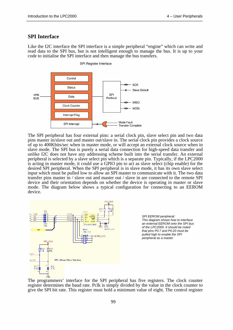
Introduction to the LPC2000 4 – User Peripherals
99
SPI Interface Like the I2C interface the SPI interface is a simple peripheral “engine” which can write and read data to the SPI bus, but is not intelligent enough to manage the bus. It is up to your code to initialise the SPI interface and then manage the bus transfers.
The SPI peripheral has four external pins: a serial clock pin, slave select pin and two data pins master in/slave out and master out/slave in. The serial clock pin provides a clock source of up to 400Kbits/sec when in master mode, or will accept an external clock source when in slave mode. The SPI bus is purely a serial data connection for high-speed data transfer and unlike I2C does not have any addressing scheme built into the serial transfer. An external peripheral is selected by a slave select pin which is a separate pin. Typically, if the LPC2000 is acting in master mode, it could use a GPIO pin to act as slave select (chip enable) for the desired SPI peripheral. When the SPI peripheral is in slave mode, it has its own slave select input which must be pulled low to allow an SPI master to communicate with it. The two data transfer pins master in / slave out and master out / slave in are connected to the remote SPI device and their orientation depends on whether the device is operating in master or slave mode. The diagram below shows a typical configuration for connecting to an EEROM device.
The programmers’ interface for the SPI peripheral has five registers. The clock counter register determines the baud rate. Pclk is simply divided by the value in the clock counter to give the SPI bit rate. This register must hold a minimum value of eight. The control register
SPI EEROM peripheral: This diagram shows how to interface an external EEROM onto the SPI bus of the LPC2000. It should be noted that pins P0.7 and P0.20 must be pulled high to enable the SPI peripheral as a master
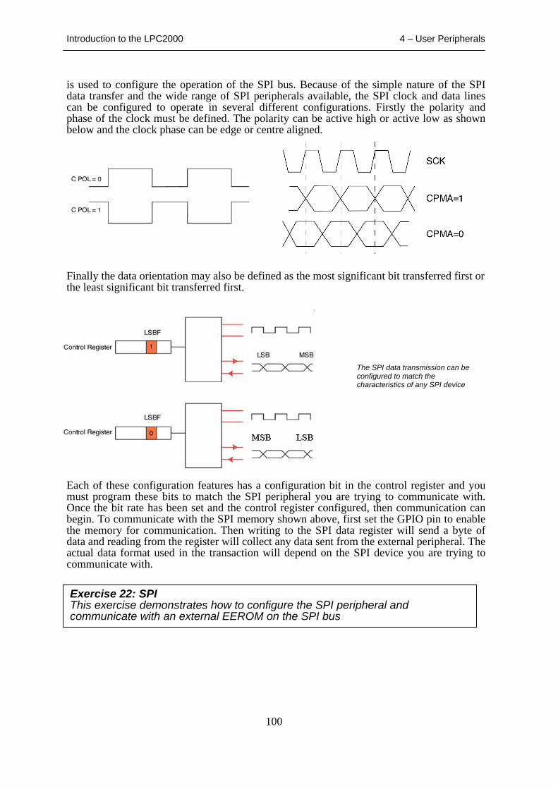
Introduction to the LPC2000 4 – User Peripherals
100
is used to configure the operation of the SPI bus. Because of the simple nature of the SPI data transfer and the wide range of SPI peripherals available, the SPI clock and data lines can be configured to operate in several different configurations. Firstly the polarity and phase of the clock must be defined. The polarity can be active high or active low as shown below and the clock phase can be edge or centre aligned. Finally the data orientation may also be defined as the most significant bit transferred first or the least significant bit transferred first.
Each of these configuration features has a configuration bit in the control register and you must program these bits to match the SPI peripheral you are trying to communicate with. Once the bit rate has been set and the control register configured, then communication can begin. To communicate with the SPI memory shown above, first set the GPIO pin to enable the memory for communication. Then writing to the SPI data register will send a byte of data and reading from the register will collect any data sent from the external peripheral. The actual data format used in the transaction will depend on the SPI device you are trying to communicate with.
The SPI data transmission can be configured to match the characteristics of any SPI device
Exercise 22: SPI This exercise demonstrates how to configure the SPI peripheral and communicate with an external EEROM on the SPI bus
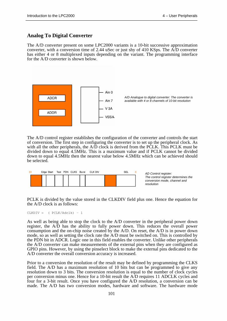
Introduction to the LPC2000 4 – User Peripherals
101
Analog To Digital Converter The A/D converter present on some LPC2000 variants is a 10-bit successive approximation converter, with a conversion time of 2.44 uSec or just shy of 410 KSps. The A/D converter has either 4 or 8 multiplexed inputs depending on the variant. The programming interface for the A/D converter is shown below.
The A/D control register establishes the configuration of the converter and controls the start of conversion. The first step in configuring the converter is to set up the peripheral clock. As with all the other peripherals, the A/D clock is derived from the PCLK. This PCLK must be divided down to equal 4.5MHz. This is a maximum value and if PCLK cannot be divided down to equal 4.5MHz then the nearest value below 4.5MHz which can be achieved should be selected.
PCLK is divided by the value stored in the CLKDIV field plus one. Hence the equation for the A/D clock is as follows: CLKDIV = ( PCLK/Adclk) - 1
As well as being able to stop the clock to the A/D converter in the peripheral power down register, the A/D has the ability to fully power down. This reduces the overall power consumption and the on-chip noise created by the A/D. On reset, the A/D is in power down mode, so as well as setting the clock rate the A/D must be switched on. This is controlled by the PDN bit in ADCR. Logic one in this field enables the converter. Unlike other peripherals the A/D converter can make measurements of the external pins when they are configured as GPIO pins. However, by using the pinselect block to make the external pins dedicated to the A/D converter the overall conversion accuracy is increased. Prior to a conversion the resolution of the result may be defined by programming the CLKS field. The A/D has a maximum resolution of 10 bits but can be programmed to give any resolution down to 3 bits. The conversion resolution is equal to the number of clock cycles per conversion minus one. Hence for a 10-bit result the A/D requires 11 ADCLK cycles and four for a 3-bit result. Once you have configured the A/D resolution, a conversion can be made. The A/D has two conversion modes, hardware and software. The hardware mode
A/D Analogue to digital converter: The converter is available with 4 or 8 channels of 10-bit resolution
AD Control register: The control register determines the conversion mode, channel and resolution
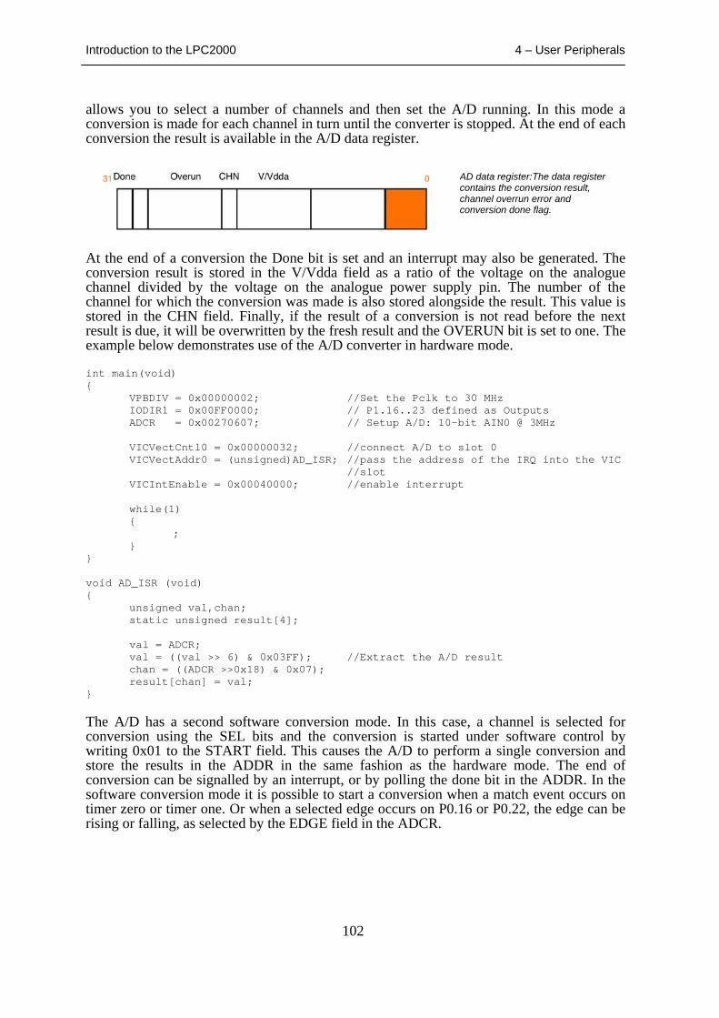
Introduction to the LPC2000 4 – User Peripherals
102
allows you to select a number of channels and then set the A/D running. In this mode a conversion is made for each channel in turn until the converter is stopped. At the end of each conversion the result is available in the A/D data register.
At the end of a conversion the Done bit is set and an interrupt may also be generated. The conversion result is stored in the V/Vdda field as a ratio of the voltage on the analogue channel divided by the voltage on the analogue power supply pin. The number of the channel for which the conversion was made is also stored alongside the result. This value is stored in the CHN field. Finally, if the result of a conversion is not read before the next result is due, it will be overwritten by the fresh result and the OVERUN bit is set to one. The example below demonstrates use of the A/D converter in hardware mode. int main(void) {
VPBDIV = 0x00000002; //Set the Pclk to 30 MHz IODIR1 = 0x00FF0000; // P1.16..23 defined as Outputs ADCR = 0x00270607; // Setup A/D: 10-bit AIN0 @ 3MHz
VICVectCntl0 = 0x00000032; //connect A/D to slot 0 VICVectAddr0 = (unsigned)AD_ISR; //pass the address of the IRQ into the VIC
//slot VICIntEnable = 0x00040000; //enable interrupt
while(1) {
; } } void AD_ISR (void) {
unsigned val,chan; static unsigned result[4];
val = ADCR; val = ((val >> 6) & 0x03FF); //Extract the A/D result chan = ((ADCR >>0x18) & 0x07); result[chan] = val;
} The A/D has a second software conversion mode. In this case, a channel is selected for conversion using the SEL bits and the conversion is started under software control by writing 0x01 to the START field. This causes the A/D to perform a single conversion and store the results in the ADDR in the same fashion as the hardware mode. The end of conversion can be signalled by an interrupt, or by polling the done bit in the ADDR. In the software conversion mode it is possible to start a conversion when a match event occurs on timer zero or timer one. Or when a selected edge occurs on P0.16 or P0.22, the edge can be rising or falling, as selected by the EDGE field in the ADCR.
AD data register:The data register contains the conversion result, channel overrun error and conversion done flag.
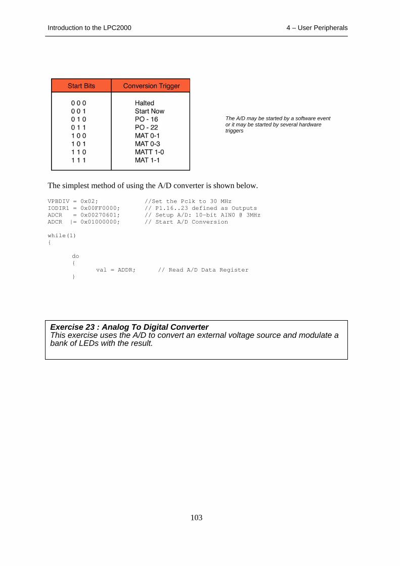
Introduction to the LPC2000 4 – User Peripherals
103
The simplest method of using the A/D converter is shown below. VPBDIV = 0x02; //Set the Pclk to 30 MHz IODIR1 = 0x00FF0000; // P1.16..23 defined as Outputs ADCR = 0x00270601; // Setup A/D: 10-bit AIN0 @ 3MHz ADCR |= 0x01000000; // Start A/D Conversion while(1) {
do {
val = ADDR; // Read A/D Data Register }
Exercise 23 : Analog To Digital ConverterThis exercise uses the A/D to convert an external voltage source and modulate a bank of LEDs with the result.
The A/D may be started by a software event or it may be started by several hardware triggers
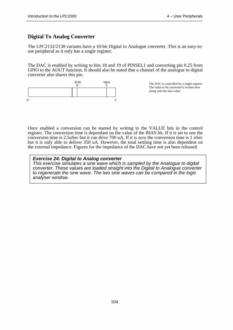
Introduction to the LPC2000 4 – User Peripherals
104
Digital To Analog Converter The LPC2132/2138 variants have a 10-bit Digital to Analogue converter. This is an easy-to-use peripheral as it only has a single register. The DAC is enabled by writing to bits 18 and 19 of PINSEL1 and converting pin 0.25 from GPIO to the AOUT function. It should also be noted that a channel of the analogue to digital converter also shares this pin.
Once enabled a conversion can be started by writing to the VALUE bits in the control register. The conversion time is dependant on the value of the BIAS bit. If it is set to one the conversion time is 2.5uSec but it can drive 700 uA. If it is zero the conversion time is 1 uSec but it is only able to deliver 350 uA. However, the total settling time is also dependent on the external impedance. Figures for the impedance of the DAC have not yet been released.
Exercise 24: Digital to Analog converterThis exercise simulates a sine wave which is sampled by the Analogue to digital converter. These values are loaded straight into the Digital to Analogue converter to regenerate the sine wave. The two sine waves can be compared in the logic analyser window.
The DAC is controlled by a single register. The value to be converted is written here along with the bias value
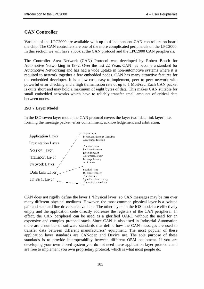
Introduction to the LPC2000 4 – User Peripherals
105
CAN Controller Variants of the LPC2000 are available with up to 4 independent CAN controllers on board the chip. The CAN controllers are one of the more complicated peripherals on the LPC2000. In this section we will have a look at the CAN protocol and the LPC2000 CAN peripherals. The Controller Area Network (CAN) Protocol was developed by Robert Bosch for Automotive Networking in 1982. Over the last 22 Years CAN has become a standard for Automotive Networking and has had a wide uptake in non-automotive systems where it is required to network together a few embedded nodes. CAN has many attractive features for the embedded developer. It is a low-cost, easy-to-implement, peer to peer network with powerful error checking and a high transmission rate of up to 1 Mbit/sec. Each CAN packet is quite short and may hold a maximum of eight bytes of data. This makes CAN suitable for small embedded networks which have to reliably transfer small amounts of critical data between nodes. ISO 7 Layer Model In the ISO seven layer model the CAN protocol covers the layer two ‘data link layer’, i.e. forming the message packet, error containment, acknowledgement and arbitration.
CAN does not rigidly define the layer 1 ‘Physical layer’ so CAN messages may be run over many different physical mediums. However, the most common physical layer is a twisted pair and standard line drivers are available. The other layers in the IOS model are effectively empty and the application code directly addresses the registers of the CAN peripheral. In effect, the CAN peripheral can be used as a glorified UART without the need for an expensive and complex protocol stack. Since CAN is also used in Industrial Automation there are a number of software standards that define how the CAN messages are used to transfer data between different manufacturers’ equipment. The most popular of these application layer standards are CANopen and Device net. The sole purpose of these standards is to provide interoperability between different OEM equipment. If you are developing your own closed system you do not need these application layer protocols and are free to implement you own proprietary protocol, which is what most people do.
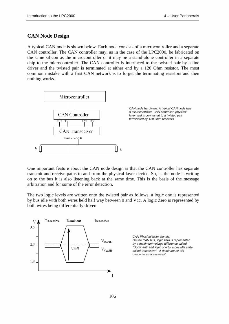
Introduction to the LPC2000 4 – User Peripherals
106
CAN Node Design A typical CAN node is shown below. Each node consists of a microcontroller and a separate CAN controller. The CAN controller may, as in the case of the LPC2000, be fabricated on the same silicon as the microcontroller or it may be a stand-alone controller in a separate chip to the microcontroller. The CAN controller is interfaced to the twisted pair by a line driver and the twisted pair is terminated at either end by a 120 Ohm resistor. The most common mistake with a first CAN network is to forget the terminating resistors and then nothing works.
One important feature about the CAN node design is that the CAN controller has separate transmit and receive paths to and from the physical layer device. So, as the node is writing on to the bus it is also listening back at the same time. This is the basis of the message arbitration and for some of the error detection. The two logic levels are written onto the twisted pair as follows, a logic one is represented by bus idle with both wires held half way between 0 and Vcc. A logic Zero is represented by both wires being differentially driven.
CAN node hardware: A typical CAN node has a microcontroller, CAN controller, physical layer and is connected to a twisted pair terminated by 120 Ohm resistors.
CAN Physical layer signals: On the CAN bus, logic zero is represented by a maximum voltage difference called “Dominant” and logic one by a bus idle state called “recessive”. A dominant bit will overwrite a recessive bit.
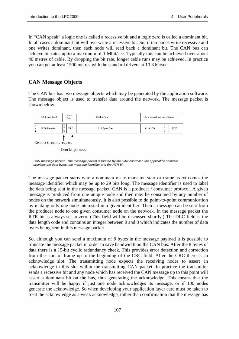
Introduction to the LPC2000 4 – User Peripherals
107
In “CAN speak” a logic one is called a recessive bit and a logic zero is called a dominant bit. In all cases a dominant bit will overwrite a recessive bit. So, if ten nodes write recessive and one writes dominant, then each node will read back a dominant bit. The CAN bus can achieve bit rates up to a maximum of 1 Mbit/sec. Typically this can be achieved over about 40 metres of cable. By dropping the bit rate, longer cable runs may be achieved. In practice you can get at least 1500 metres with the standard drivers at 10 Kbit/sec. CAN Message Objects The CAN bus has two message objects which may be generated by the application software. The message object is used to transfer data around the network. The message packet is shown below.
The message packet starts with a dominant bit to mark the start of frame. Next comes the message identifier which may be up to 29 bits long. The message identifier is used to label the data being sent in the message packet. CAN is a producer / consumer protocol. A given message is produced from one unique node and then may be consumed by any number of nodes on the network simultaneously. It is also possible to do point-to-point communication by making only one node interested in a given identifier. Then a message can be sent from the producer node to one given consumer node on the network. In the message packet the RTR bit is always set to zero. (This field will be discussed shortly.) The DLC field is the data length code and contains an integer between 0 and 8 which indicates the number of data bytes being sent in this message packet. So, although you can send a maximum of 8 bytes in the message payload it is possible to truncate the message packet in order to save bandwidth on the CAN bus. After the 8 bytes of data there is a 15-bit cyclic redundancy check. This provides error detection and correction from the start of frame up to the beginning of the CRC field. After the CRC there is an acknowledge slot. The transmitting node expects the receiving nodes to assert an acknowledge in this slot within the transmitting CAN packet. In practice the transmitter sends a recessive bit and any node which has received the CAN message up to this point will assert a dominant bit on the bus, thus generating the acknowledge. This means that the transmitter will be happy if just one node acknowledges its message, or if 100 nodes generate the acknowledge. So when developing your application layer care must be taken to treat the acknowledge as a weak acknowledge, rather than confirmation that the message has
CAN message packet : The message packet is formed by the CAN controller, the application software provides the data bytes, the message identifier and the RTR bit
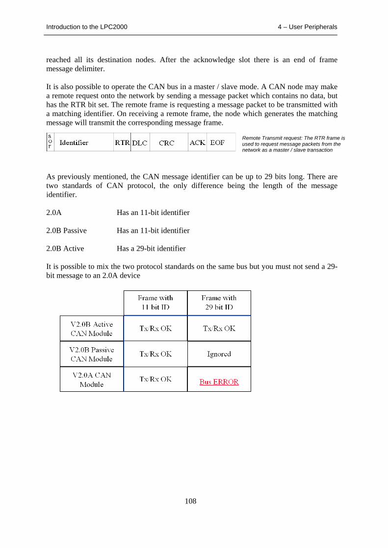
Introduction to the LPC2000 4 – User Peripherals
108
reached all its destination nodes. After the acknowledge slot there is an end of frame message delimiter. It is also possible to operate the CAN bus in a master / slave mode. A CAN node may make a remote request onto the network by sending a message packet which contains no data, but has the RTR bit set. The remote frame is requesting a message packet to be transmitted with a matching identifier. On receiving a remote frame, the node which generates the matching message will transmit the corresponding message frame.
As previously mentioned, the CAN message identifier can be up to 29 bits long. There are two standards of CAN protocol, the only difference being the length of the message identifier. 2.0A Has an 11-bit identifier 2.0B Passive Has an 11-bit identifier 2.0B Active Has a 29-bit identifier It is possible to mix the two protocol standards on the same bus but you must not send a 29- bit message to an 2.0A device
Remote Transmit request: The RTR frame is used to request message packets from the network as a master / slave transaction
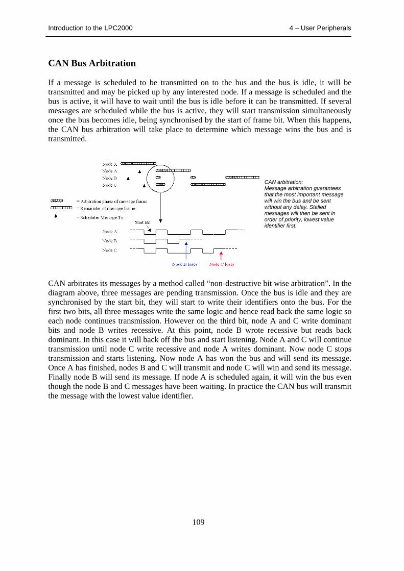
Introduction to the LPC2000 4 – User Peripherals
109
CAN Bus Arbitration If a message is scheduled to be transmitted on to the bus and the bus is idle, it will be transmitted and may be picked up by any interested node. If a message is scheduled and the bus is active, it will have to wait until the bus is idle before it can be transmitted. If several messages are scheduled while the bus is active, they will start transmission simultaneously once the bus becomes idle, being synchronised by the start of frame bit. When this happens, the CAN bus arbitration will take place to determine which message wins the bus and is transmitted.
CAN arbitrates its messages by a method called “non-destructive bit wise arbitration”. In the diagram above, three messages are pending transmission. Once the bus is idle and they are synchronised by the start bit, they will start to write their identifiers onto the bus. For the first two bits, all three messages write the same logic and hence read back the same logic so each node continues transmission. However on the third bit, node A and C write dominant bits and node B writes recessive. At this point, node B wrote recessive but reads back dominant. In this case it will back off the bus and start listening. Node A and C will continue transmission until node C write recessive and node A writes dominant. Now node C stops transmission and starts listening. Now node A has won the bus and will send its message. Once A has finished, nodes B and C will transmit and node C will win and send its message. Finally node B will send its message. If node A is scheduled again, it will win the bus even though the node B and C messages have been waiting. In practice the CAN bus will transmit the message with the lowest value identifier.
CAN arbitration: Message arbitration guarantees that the most important message will win the bus and be sent without any delay. Stalled messages will then be sent in order of priority, lowest value identifier first.
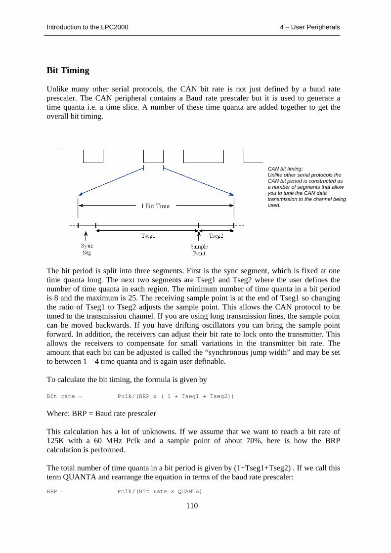
Introduction to the LPC2000 4 – User Peripherals
110
Bit Timing Unlike many other serial protocols, the CAN bit rate is not just defined by a baud rate prescaler. The CAN peripheral contains a Baud rate prescaler but it is used to generate a time quanta i.e. a time slice. A number of these time quanta are added together to get the overall bit timing.
The bit period is split into three segments. First is the sync segment, which is fixed at one time quanta long. The next two segments are Tseg1 and Tseg2 where the user defines the number of time quanta in each region. The minimum number of time quanta in a bit period is 8 and the maximum is 25. The receiving sample point is at the end of Tseg1 so changing the ratio of Tseg1 to Tseg2 adjusts the sample point. This allows the CAN protocol to be tuned to the transmission channel. If you are using long transmission lines, the sample point can be moved backwards. If you have drifting oscillators you can bring the sample point forward. In addition, the receivers can adjust their bit rate to lock onto the transmitter. This allows the receivers to compensate for small variations in the transmitter bit rate. The amount that each bit can be adjusted is called the “synchronous jump width” and may be set to between 1 – 4 time quanta and is again user definable. To calculate the bit timing, the formula is given by Bit rate = Pclk/(BRP x ( 1 + Tseg1 + Tseg2))
Where: BRP = Baud rate prescaler This calculation has a lot of unknowns. If we assume that we want to reach a bit rate of 125K with a 60 MHz Pclk and a sample point of about 70%, here is how the BRP calculation is performed. The total number of time quanta in a bit period is given by (1+Tseg1+Tseg2) . If we call this term QUANTA and rearrange the equation in terms of the baud rate prescaler: BRP = Pclk/(Bit rate x QUANTA)
CAN bit timing: Unlike other serial protocols the CAN bit period is constructed as a number of segments that allow you to tune the CAN data transmission to the channel being used.

Introduction to the LPC2000 4 – User Peripherals
111
Using our known values: BRP = 60 MHz/(125K x QUANTA)
Now we know that we can have between 8 and 25 time quanta in the bit period, so using a spreadsheet we can substitute in integer values between 8 and 25 for QUANTA until we get an integer value for BRP. In this case when QUANTA = 16 BRP = 30; Then 16 = Quanta = ( 1+Tseg1+Tseg2) So we can adjust the ratio between Tseg1 and Tseg2 to give us the desired sample point. Sample point = (QUANTA x 70)/100 Hence 16 *0.7 = 11.2. This gives Tseg 1 = 10, Tseg2 = 5 and the sample point = 68.8% The value for the synchronous jump width may be calculated via the following rule of thumb. Tseg2 >= 5 Tq then program SJW to 4 Tseg2 < 5 Tq then program SJW to (Tseg2 - 1) Tq In this case SJW = 4.
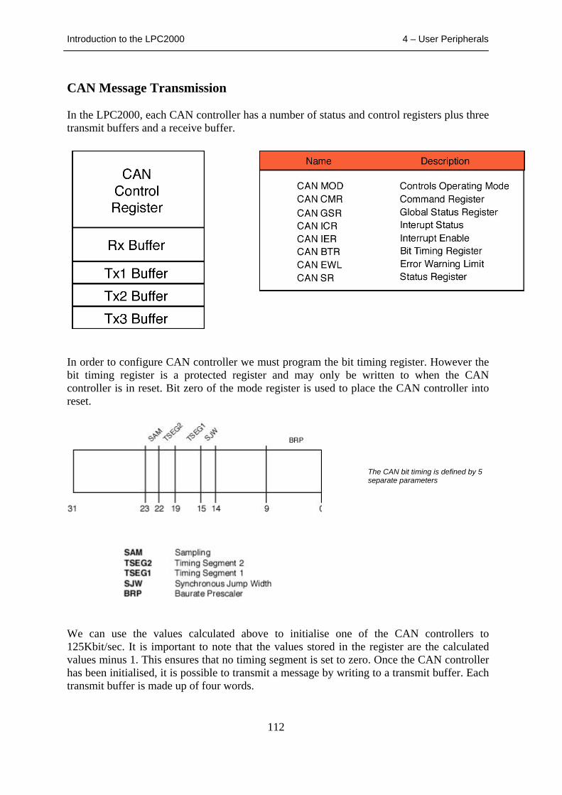
Introduction to the LPC2000 4 – User Peripherals
112
CAN Message Transmission In the LPC2000, each CAN controller has a number of status and control registers plus three transmit buffers and a receive buffer.
In order to configure CAN controller we must program the bit timing register. However the bit timing register is a protected register and may only be written to when the CAN controller is in reset. Bit zero of the mode register is used to place the CAN controller into reset.
We can use the values calculated above to initialise one of the CAN controllers to 125Kbit/sec. It is important to note that the values stored in the register are the calculated values minus 1. This ensures that no timing segment is set to zero. Once the CAN controller has been initialised, it is possible to transmit a message by writing to a transmit buffer. Each transmit buffer is made up of four words.
The CAN bit timing is defined by 5 separate parameters
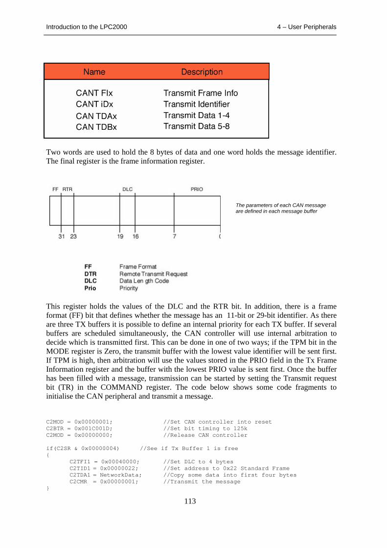
Introduction to the LPC2000 4 – User Peripherals
113
Two words are used to hold the 8 bytes of data and one word holds the message identifier. The final register is the frame information register.
This register holds the values of the DLC and the RTR bit. In addition, there is a frame format (FF) bit that defines whether the message has an 11-bit or 29-bit identifier. As there are three TX buffers it is possible to define an internal priority for each TX buffer. If several buffers are scheduled simultaneously, the CAN controller will use internal arbitration to decide which is transmitted first. This can be done in one of two ways; if the TPM bit in the MODE register is Zero, the transmit buffer with the lowest value identifier will be sent first. If TPM is high, then arbitration will use the values stored in the PRIO field in the Tx Frame Information register and the buffer with the lowest PRIO value is sent first. Once the buffer has been filled with a message, transmission can be started by setting the Transmit request bit (TR) in the COMMAND register. The code below shows some code fragments to initialise the CAN peripheral and transmit a message. C2MOD = 0x00000001; //Set CAN controller into reset C2BTR = 0x001C001D; //Set bit timing to 125k C2MOD = 0x00000000; //Release CAN controller if(C2SR & 0x00000004) //See if Tx Buffer 1 is free {
C2TFI1 = 0x00040000; //Set DLC to 4 bytes C2TID1 = 0x00000022; //Set address to 0x22 Standard Frame C2TDA1 = NetworkData; //Copy some data into first four bytes C2CMR = 0x00000001; //Transmit the message
}
The parameters of each CAN message are defined in each message buffer

Introduction to the LPC2000 4 – User Peripherals
114
Exercise 25: CAN Transmit This exercise configures the second CAN channel for 125K bits\second and repeatedly transmits a CAN message frame.
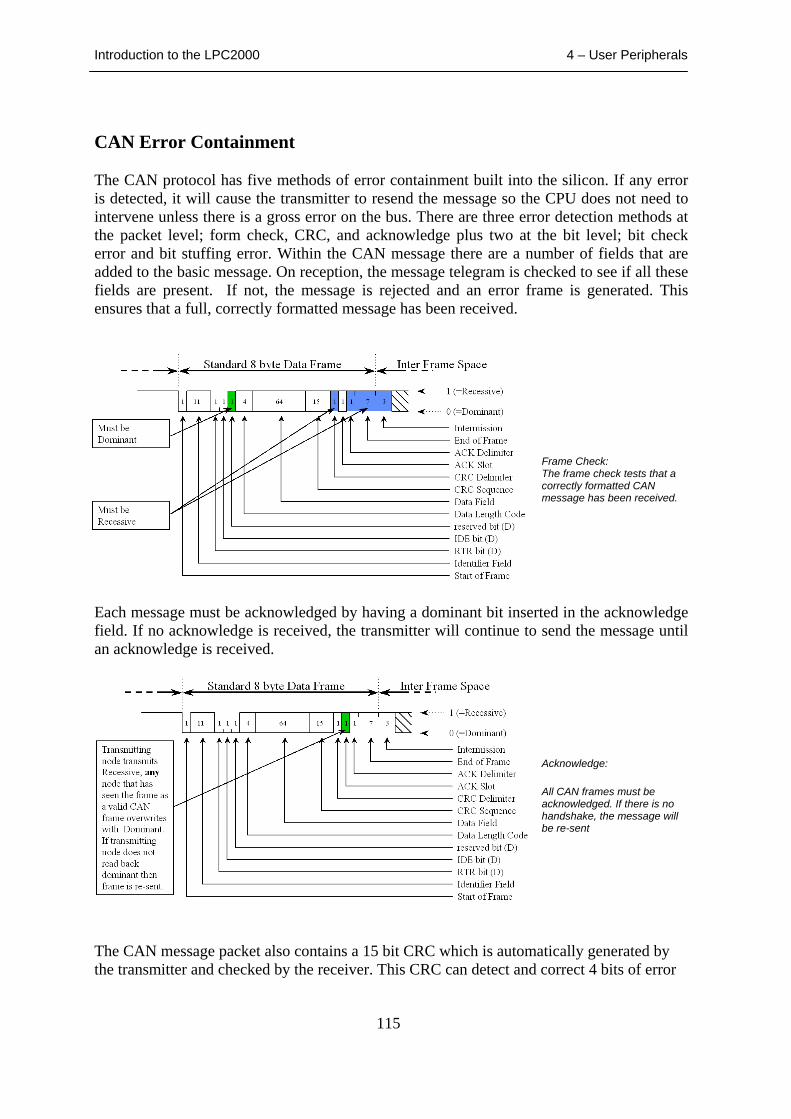
Introduction to the LPC2000 4 – User Peripherals
115
CAN Error Containment The CAN protocol has five methods of error containment built into the silicon. If any error is detected, it will cause the transmitter to resend the message so the CPU does not need to intervene unless there is a gross error on the bus. There are three error detection methods at the packet level; form check, CRC, and acknowledge plus two at the bit level; bit check error and bit stuffing error. Within the CAN message there are a number of fields that are added to the basic message. On reception, the message telegram is checked to see if all these fields are present. If not, the message is rejected and an error frame is generated. This ensures that a full, correctly formatted message has been received.
Each message must be acknowledged by having a dominant bit inserted in the acknowledge field. If no acknowledge is received, the transmitter will continue to send the message until an acknowledge is received.
The CAN message packet also contains a 15 bit CRC which is automatically generated by the transmitter and checked by the receiver. This CRC can detect and correct 4 bits of error
Frame Check: The frame check tests that a correctly formatted CAN message has been received.
Acknowledge:
All CAN frames must be acknowledged. If there is no handshake, the message will be re-sent
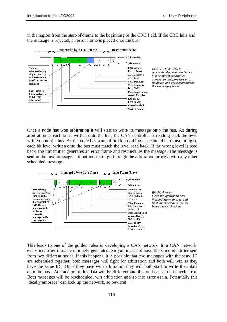
Introduction to the LPC2000 4 – User Peripherals
116
in the region from the start-of-frame to the beginning of the CRC field. If the CRC fails and the message is rejected, an error frame is placed onto the bus.
Once a node has won arbitration it will start to write its message onto the bus. As during arbitration as each bit is written onto the bus, the CAN controller is reading back the level written onto the bus. As the node has won arbitration nothing else should be transmitting so each bit level written onto the bus must match the level read back. If the wrong level is read back, the transmitter generates an error frame and reschedules the message. The message is sent in the next message slot but must still go through the arbitration process with any other scheduled message.
This leads to one of the golden rules in developing a CAN network. In a CAN network, every identifier must be uniquely generated. So you must not have the same identifier sent from two different nodes. If this happens, it is possible that two messages with the same ID are scheduled together, both messages will fight for arbitration and both will win as they have the same ID. Once they have won arbitration they will both start to write their data onto the bus. At some point this data will be different and this will cause a bit check error. Both messages will be rescheduled, win arbitration and go into error again. Potentially this ‘deadly embrace’ can lock up the network, so beware!
CRC: A 15 bit CRC is automatically generated which is a weighted polynomial checksum that provides error detection and correction across the message packet
Bit check error: Once the arbitration has finished the write and read back mechanism is use for bitwise error checking
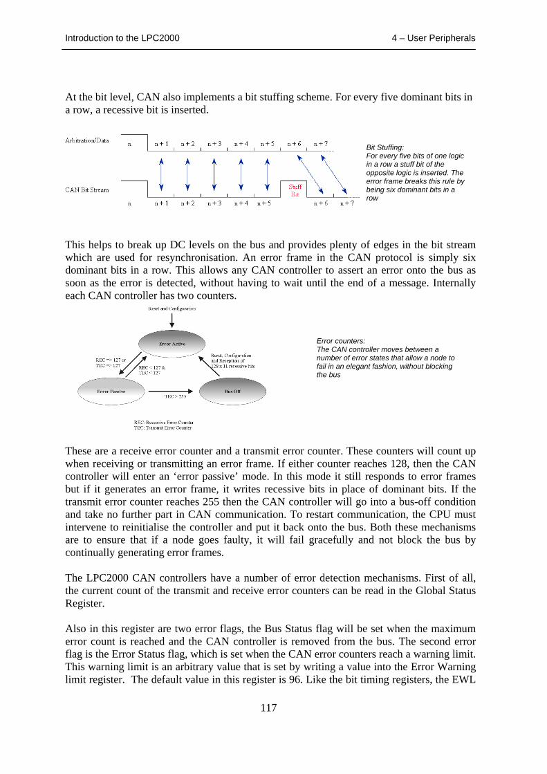
Introduction to the LPC2000 4 – User Peripherals
117
At the bit level, CAN also implements a bit stuffing scheme. For every five dominant bits in a row, a recessive bit is inserted.
This helps to break up DC levels on the bus and provides plenty of edges in the bit stream which are used for resynchronisation. An error frame in the CAN protocol is simply six dominant bits in a row. This allows any CAN controller to assert an error onto the bus as soon as the error is detected, without having to wait until the end of a message. Internally each CAN controller has two counters.
These are a receive error counter and a transmit error counter. These counters will count up when receiving or transmitting an error frame. If either counter reaches 128, then the CAN controller will enter an ‘error passive’ mode. In this mode it still responds to error frames but if it generates an error frame, it writes recessive bits in place of dominant bits. If the transmit error counter reaches 255 then the CAN controller will go into a bus-off condition and take no further part in CAN communication. To restart communication, the CPU must intervene to reinitialise the controller and put it back onto the bus. Both these mechanisms are to ensure that if a node goes faulty, it will fail gracefully and not block the bus by continually generating error frames. The LPC2000 CAN controllers have a number of error detection mechanisms. First of all, the current count of the transmit and receive error counters can be read in the Global Status Register. Also in this register are two error flags, the Bus Status flag will be set when the maximum error count is reached and the CAN controller is removed from the bus. The second error flag is the Error Status flag, which is set when the CAN error counters reach a warning limit. This warning limit is an arbitrary value that is set by writing a value into the Error Warning limit register. The default value in this register is 96. Like the bit timing registers, the EWL
Bit Stuffing: For every five bits of one logic in a row a stuff bit of the opposite logic is inserted. The error frame breaks this rule by being six dominant bits in a row
Error counters: The CAN controller moves between a number of error states that allow a node to fail in an elegant fashion, without blocking the bus
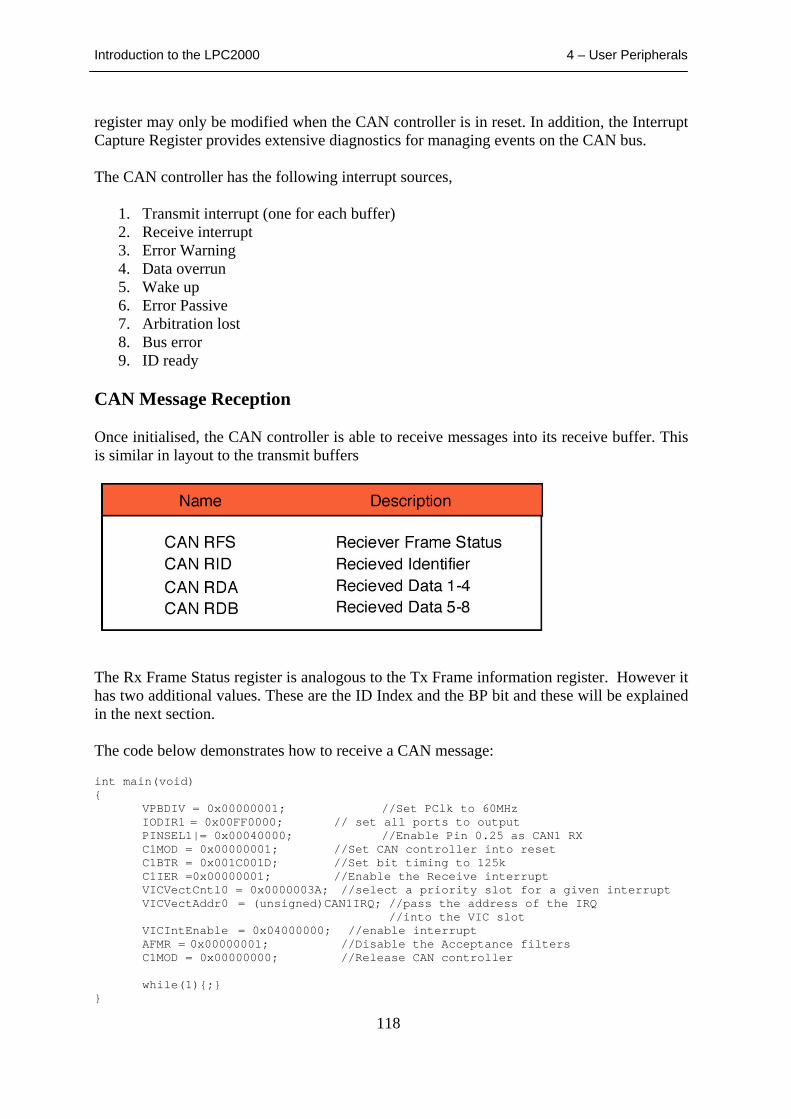
Introduction to the LPC2000 4 – User Peripherals
118
register may only be modified when the CAN controller is in reset. In addition, the Interrupt Capture Register provides extensive diagnostics for managing events on the CAN bus. The CAN controller has the following interrupt sources,
1. Transmit interrupt (one for each buffer) 2. Receive interrupt 3. Error Warning 4. Data overrun 5. Wake up 6. Error Passive 7. Arbitration lost 8. Bus error 9. ID ready
CAN Message Reception Once initialised, the CAN controller is able to receive messages into its receive buffer. This is similar in layout to the transmit buffers
The Rx Frame Status register is analogous to the Tx Frame information register. However it has two additional values. These are the ID Index and the BP bit and these will be explained in the next section. The code below demonstrates how to receive a CAN message: int main(void) {
VPBDIV = 0x00000001; //Set PClk to 60MHz IODIR1 = 0x00FF0000; // set all ports to output PINSEL1|= 0x00040000; //Enable Pin 0.25 as CAN1 RX C1MOD = 0x00000001; //Set CAN controller into reset C1BTR = 0x001C001D; //Set bit timing to 125k C1IER =0x00000001; //Enable the Receive interrupt VICVectCntl0 = 0x0000003A; //select a priority slot for a given interrupt VICVectAddr0 = (unsigned)CAN1IRQ; //pass the address of the IRQ
//into the VIC slot VICIntEnable = 0x04000000; //enable interrupt AFMR = 0x00000001; //Disable the Acceptance filters C1MOD = 0x00000000; //Release CAN controller
while(1){;}
}
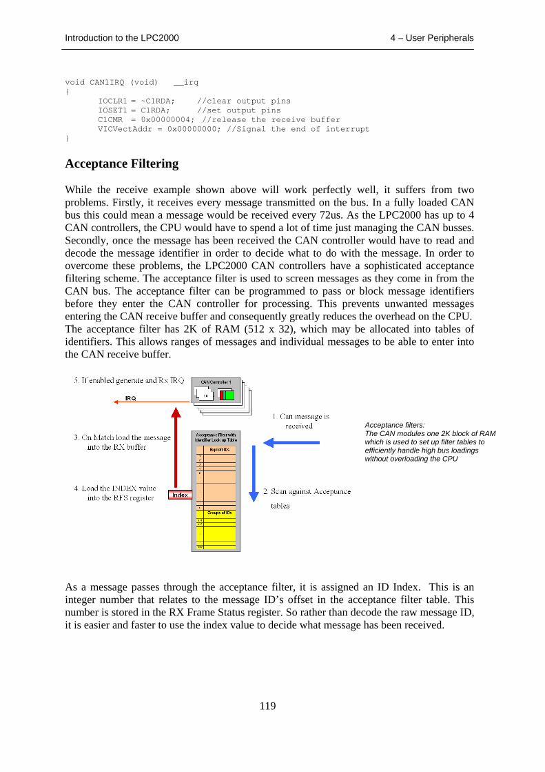
Introduction to the LPC2000 4 – User Peripherals
119
void CAN1IRQ (void) __irq {
IOCLR1 = ~C1RDA; //clear output pins IOSET1 = C1RDA; //set output pins C1CMR = 0x00000004; //release the receive buffer VICVectAddr = 0x00000000; //Signal the end of interrupt
}
Acceptance Filtering While the receive example shown above will work perfectly well, it suffers from two problems. Firstly, it receives every message transmitted on the bus. In a fully loaded CAN bus this could mean a message would be received every 72us. As the LPC2000 has up to 4 CAN controllers, the CPU would have to spend a lot of time just managing the CAN busses. Secondly, once the message has been received the CAN controller would have to read and decode the message identifier in order to decide what to do with the message. In order to overcome these problems, the LPC2000 CAN controllers have a sophisticated acceptance filtering scheme. The acceptance filter is used to screen messages as they come in from the CAN bus. The acceptance filter can be programmed to pass or block message identifiers before they enter the CAN controller for processing. This prevents unwanted messages entering the CAN receive buffer and consequently greatly reduces the overhead on the CPU. The acceptance filter has 2K of RAM (512 x 32), which may be allocated into tables of identifiers. This allows ranges of messages and individual messages to be able to enter into the CAN receive buffer.
As a message passes through the acceptance filter, it is assigned an ID Index. This is an integer number that relates to the message ID’s offset in the acceptance filter table. This number is stored in the RX Frame Status register. So rather than decode the raw message ID, it is easier and faster to use the index value to decide what message has been received.
Acceptance filters: The CAN modules one 2K block of RAM which is used to set up filter tables to efficiently handle high bus loadings without overloading the CPU
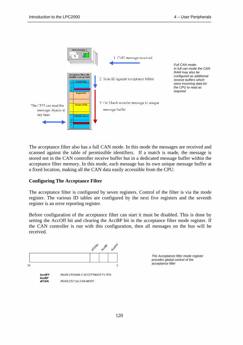
Introduction to the LPC2000 4 – User Peripherals
120
The acceptance filter also has a full CAN mode. In this mode the messages are received and scanned against the table of permissible identifiers. If a match is made, the message is stored not in the CAN controller receive buffer but in a dedicated message buffer within the acceptance filter memory. In this mode, each message has its own unique message buffer at a fixed location, making all the CAN data easily accessible from the CPU. Configuring The Acceptance Filter The acceptance filter is configured by seven registers. Control of the filter is via the mode register. The various ID tables are configured by the next five registers and the seventh register is an error reporting register. Before configuration of the acceptance filter can start it must be disabled. This is done by setting the AccOff bit and clearing the AccBP bit in the acceptance filter mode register. If the CAN controller is run with this configuration, then all messages on the bus will be received.
The Acceptance filter mode register provides global control of the acceptance filter
Full CAN mode: In full can mode the CAN RAM may also be configured as additional receive buffers which store incoming data for the CPU to read as required
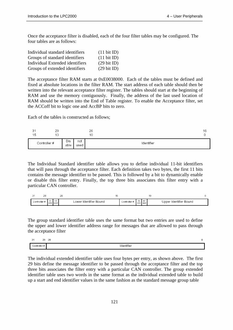
Introduction to the LPC2000 4 – User Peripherals
121
Once the acceptance filter is disabled, each of the four filter tables may be configured. The four tables are as follows: Individual standard identifiers (11 bit ID) Groups of standard identifiers (11 bit ID) Individual Extended identifiers (29 bit ID) Groups of extended identifiers (29 bit ID) The acceptance filter RAM starts at 0xE0038000. Each of the tables must be defined and fixed at absolute locations in the filter RAM. The start address of each table should then be written into the relevant acceptance filter register. The tables should start at the beginning of RAM and use the memory contiguously. Finally, the address of the last used location of RAM should be written into the End of Table register. To enable the Acceptance filter, set the ACCoff bit to logic one and AccBP bits to zero. Each of the tables is constructed as follows;
The Individual Standard identifier table allows you to define individual 11-bit identifiers that will pass through the acceptance filter. Each definition takes two bytes, the first 11 bits contains the message identifier to be passed. This is followed by a bit to dynamically enable or disable this filter entry. Finally, the top three bits associates this filter entry with a particular CAN controller.
The group standard identifier table uses the same format but two entries are used to define the upper and lower identifier address range for messages that are allowed to pass through the acceptance filter
The individual extended identifier table uses four bytes per entry, as shown above. The first 29 bits define the message identifier to be passed through the acceptance filter and the top three bits associates the filter entry with a particular CAN controller. The group extended identifier table uses two words in the same format as the individual extended table to build up a start and end identifier values in the same fashion as the standard message group table
Introduction to the LPC2000 4 – User Peripherals
122
The following code shows how the acceptance filters may be configured for the basic CAN mode. unsigned int StandardFilter[2] _at_ 0xE0038000; //Declare the standard //acceptance filter table unsigned int GroupStdFilter[2] _at_ 0xE0038008; //Next the standard Group //filter table unsigned int IndividualExtFilter[2] _at_ 0xE0038010; //Now the extended filter //table unsigned int GroupExtFilter[2] _at_ 0xE0038018; //Finally the Group extended //filter table AFMR = 0x00000001; //Disable the Acceptance filters StandardFilter[0] = 0x20012002; //Setup the standard filter table StandardFilter[1] = 0x20032004; //Allow Ids 1,2,3 & 4 SFF_sa = 0x00000000; //Set start address of Standard table SFF_GRP_sa = 0x00000008; //Set start address of Standard group table EFF_sa = 0x00000008; //Set start address of Extended table EFF_GRP_sa = 0x00000008; //Set start address of Extended group table ENDofTable = 0x00000008; //Set end of table address AFMR = 0x00000000; //Enable Acceptance filters C1MOD = 0x00000000; //Release CAN controller Summary This chapter is a bit of a moving target! The LPC2000 is a rapidly growing family with new variants being released on a regular basis. Check the CD that came with this book for a .PDF update to this chapter or keep an eye on the web at http://www.hitex.co.uk/arm/lpcbook If you have worked through this and the proceeding chapters, you should now have a firm grasp of the LPC2000 family the ARM7 CPU and the necessary development tools. Appendix B lists further reading and web resources for the ARM7 and the LPC2000 in particular.
Exercise 26 CAN Receive Like the last exercise this example configures the CAN peripheral for 125Kbits/sec and sets the acceptance filters to receive one of three message frames.

Introduction to the LPC2000 4 – User Peripherals
123
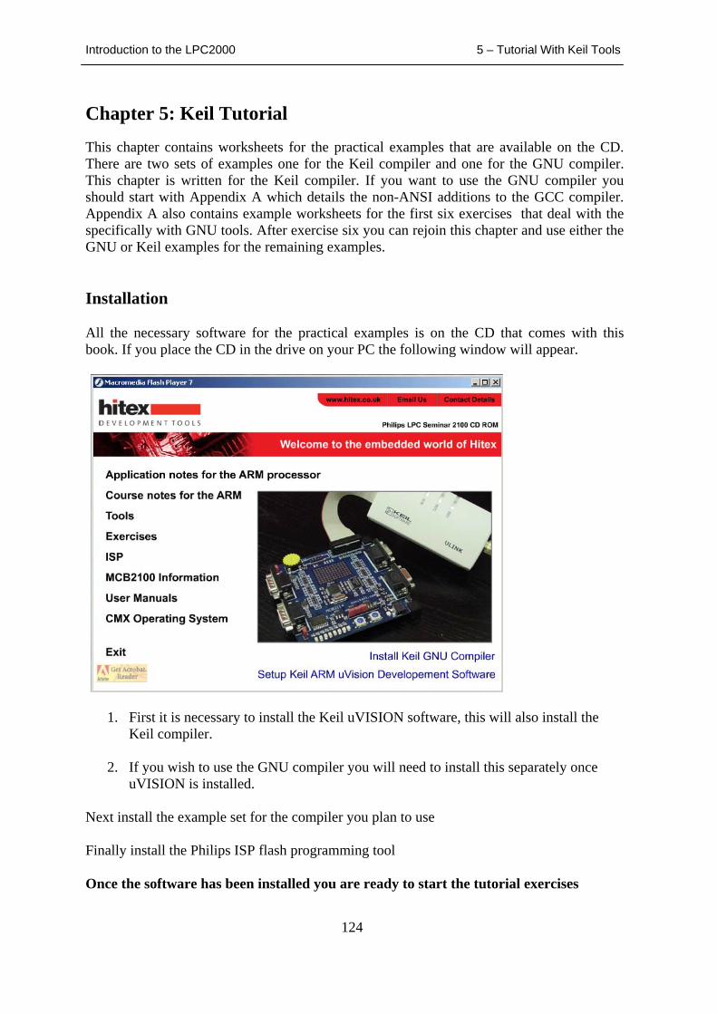
Introduction to the LPC2000 5 – Tutorial With Keil Tools
124
Chapter 5: Keil Tutorial This chapter contains worksheets for the practical examples that are available on the CD. There are two sets of examples one for the Keil compiler and one for the GNU compiler. This chapter is written for the Keil compiler. If you want to use the GNU compiler you should start with Appendix A which details the non-ANSI additions to the GCC compiler. Appendix A also contains example worksheets for the first six exercises that deal with the specifically with GNU tools. After exercise six you can rejoin this chapter and use either the GNU or Keil examples for the remaining examples. Installation All the necessary software for the practical examples is on the CD that comes with this book. If you place the CD in the drive on your PC the following window will appear.
1. First it is necessary to install the Keil uVISION software, this will also install the
Keil compiler.
2. If you wish to use the GNU compiler you will need to install this separately once uVISION is installed.
Next install the example set for the compiler you plan to use Finally install the Philips ISP flash programming tool Once the software has been installed you are ready to start the tutorial exercises
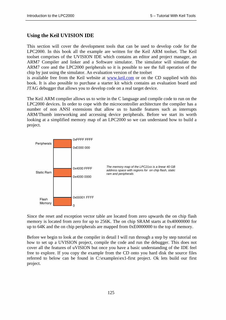
Introduction to the LPC2000 5 – Tutorial With Keil Tools
125
Using the Keil UVISION IDE This section will cover the development tools that can be used to develop code for the LPC2000. In this book all the example are written for the Keil ARM toolset. The Keil toolset comprises of the UVISION IDE which contains an editor and project manager, an ARM7 Compiler and linker and a Software simulator. The simulator will simulate the ARM7 core and the LPC2000 peripherals so it is possible to see the full operation of the chip by just using the simulator. An evaluation version of the toolset is available free from the Keil website at www.keil.com or on the CD supplied with this book. It is also possible to purchase a starter kit which contains an evaluation board and JTAG debugger that allows you to develop code on a real target device. The Keil ARM compiler allows us to write in the C language and compile code to run on the LPC2000 devices. In order to cope with the microcontroller architecture the compiler has a number of non ANSI extensions that allow us to handle features such as interrupts ARM/Thumb interworking and accessing device peripherals. Before we start its worth looking at a simplified memory map of an LPC2000 so we can understand how to build a project.
Since the reset and exception vector table are located from zero upwards the on chip flash memory is located from zero for up to 256K. The on chip SRAM starts at 0x40000000 for up to 64K and the on chip peripherals are mapped from 0xE0000000 to the top of memory. Before we begin to look at the compiler in detail I will run through a step by step tutorial on how to set up a UVISION project, compile the code and run the debugger. This does not cover all the features of uVISION but once you have a basic understanding of the IDE feel free to explore. If you copy the example from the CD onto you hard disk the source files referred to below can be found in C:\examples\ex1-first project. Ok lets build our first project.
The memory map of the LPC21xx is a linear 40 GB address space with regions for on chip flash, static ram and peripherals
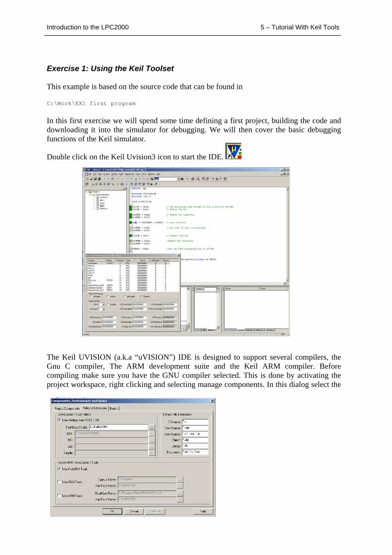
Introduction to the LPC2000 5 – Tutorial With Keil Tools
126
Exercise 1: Using the Keil Toolset This example is based on the source code that can be found in C:\Work\EX1 first program
In this first exercise we will spend some time defining a first project, building the code and downloading it into the simulator for debugging. We will then cover the basic debugging functions of the Keil simulator.
Double click on the Keil Uvision3 icon to start the IDE. The Keil UVISION (a.k.a “uVISION”) IDE is designed to support several compilers, the Gnu C compiler, The ARM development suite and the Keil ARM compiler. Before compiling make sure you have the GNU compiler selected. This is done by activating the project workspace, right clicking and selecting manage components. In this dialog select the
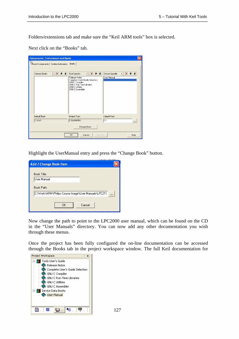
Introduction to the LPC2000 5 – Tutorial With Keil Tools
127
Folders/extensions tab and make sure the “Keil ARM tools” box is selected. Next click on the “Books” tab.
Highlight the UserManual entry and press the “Change Book” button.
Now change the path to point to the LPC2000 user manual, which can be found on the CD in the “User Manuals” directory. You can now add any other documentation you wish through these menus. Once the project has been fully configured the on-line documentation can be accessed through the Books tab in the project workspace window. The full Keil documentation for
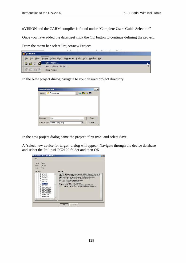
Introduction to the LPC2000 5 – Tutorial With Keil Tools
128
uVISION and the CARM compiler is found under “Complete Users Guide Selection” Once you have added the datasheet click the OK button to continue defining the project. From the menu bar select Project\new Project.
In the New project dialog navigate to your desired project directory.
In the new project dialog name the project “first.uv2” and select Save. A ‘select new device for target’ dialog will appear. Navigate through the device database and select the Philips\LPC2129 folder and then OK.
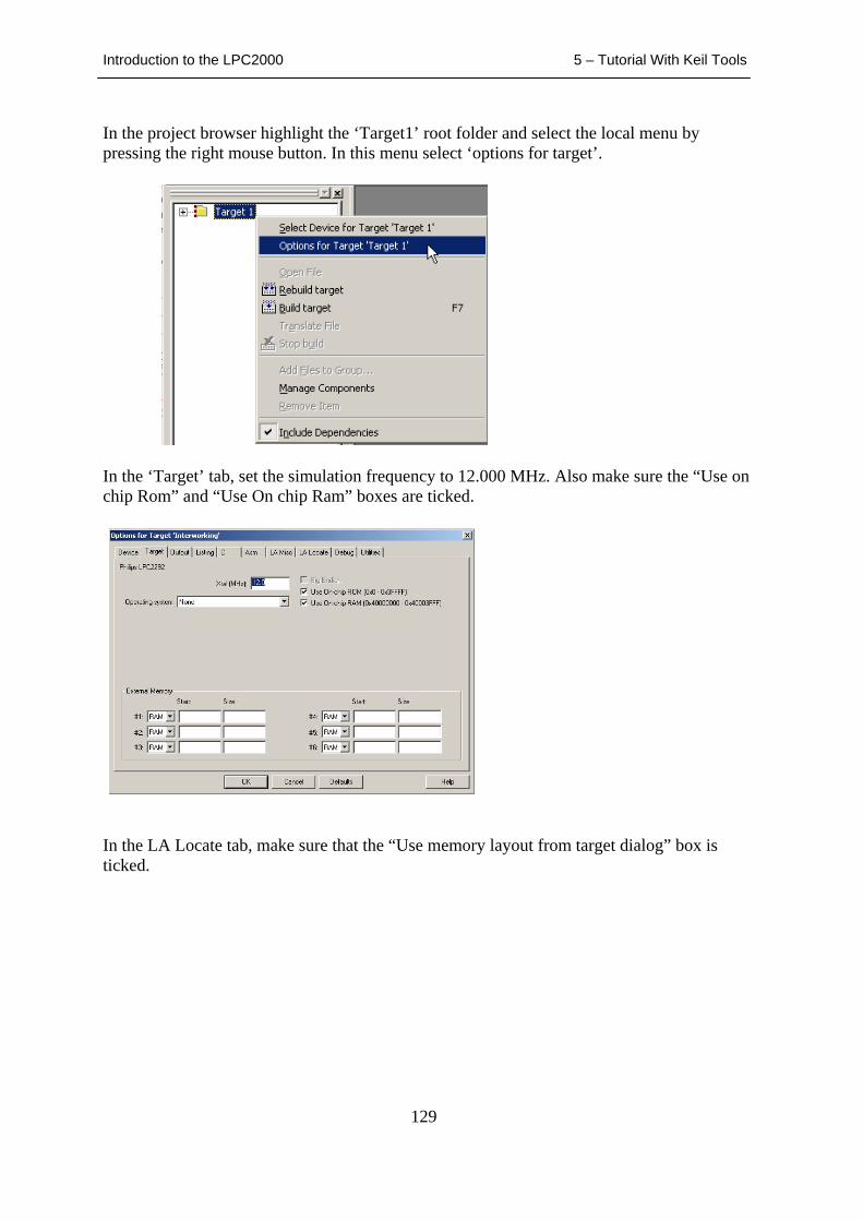
Introduction to the LPC2000 5 – Tutorial With Keil Tools
129
In the project browser highlight the ‘Target1’ root folder and select the local menu by pressing the right mouse button. In this menu select ‘options for target’.
In the ‘Target’ tab, set the simulation frequency to 12.000 MHz. Also make sure the “Use on chip Rom” and “Use On chip Ram” boxes are ticked.
In the LA Locate tab, make sure that the “Use memory layout from target dialog” box is ticked.
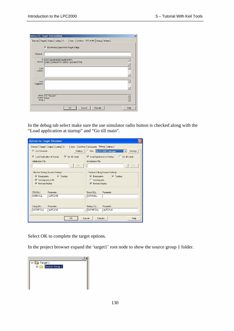
Introduction to the LPC2000 5 – Tutorial With Keil Tools
130
In the debug tab select make sure the use simulator radio button is checked along with the “Load application at startup” and “Go till main”.
Select OK to complete the target options. In the project browser expand the ‘target1’ root node to show the source group 1 folder.
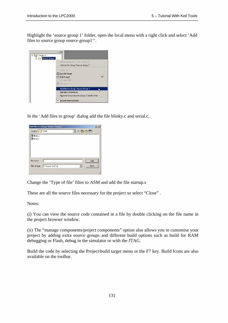
Introduction to the LPC2000 5 – Tutorial With Keil Tools
131
Highlight the ‘source group 1’ folder, open the local menu with a right click and select ‘Add files to source group source group1’’.
In the ‘Add files to group’ dialog add the file blinky.c and serial.c.
Change the ‘Type of file’ filter to ASM and add the file startup.s These are all the source files necessary for the project so select “Close” . Notes: (i) You can view the source code contained in a file by double clicking on the file name in the project browser window. (ii) The “manage components/project components” option also allows you to customise your project by adding extra source groups and different build options such as build for RAM debugging or Flash, debug in the simulator or with the JTAG. Build the code by selecting the Project\build target menu or the F7 key. Build Icons are also available on the toolbar.

Introduction to the LPC2000 5 – Tutorial With Keil Tools
132
For the rest of the tutorial, the projects will be defined but relevant bits of code will be missing. A complete copy of the exercise can be found in the solution directory. All the example code is included on your CD.
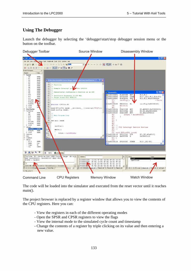
Introduction to the LPC2000 5 – Tutorial With Keil Tools
133
Using The Debugger Launch the debugger by selecting the ‘debugger\start/stop debugger session menu or the button on the toolbar.
The code will be loaded into the simulator and executed from the reset vector until it reaches main(). The project browser is replaced by a register window that allows you to view the contents of the CPU registers. Here you can: - View the registers in each of the different operating modes - Open the SPSR and CPSR registers to view the flags - View the internal mode to the simulated cycle count and timestamp
- Change the contents of a register by triple clicking on its value and then entering a new value.
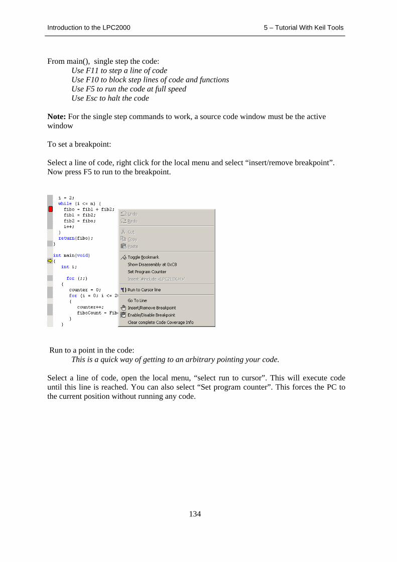
Introduction to the LPC2000 5 – Tutorial With Keil Tools
134
From main(), single step the code: Use F11 to step a line of code Use F10 to block step lines of code and functions
Use F5 to run the code at full speed Use Esc to halt the code Note: For the single step commands to work, a source code window must be the active window To set a breakpoint: Select a line of code, right click for the local menu and select “insert/remove breakpoint”. Now press F5 to run to the breakpoint.
Run to a point in the code: This is a quick way of getting to an arbitrary pointing your code. Select a line of code, open the local menu, “select run to cursor”. This will execute code until this line is reached. You can also select “Set program counter”. This forces the PC to the current position without running any code.
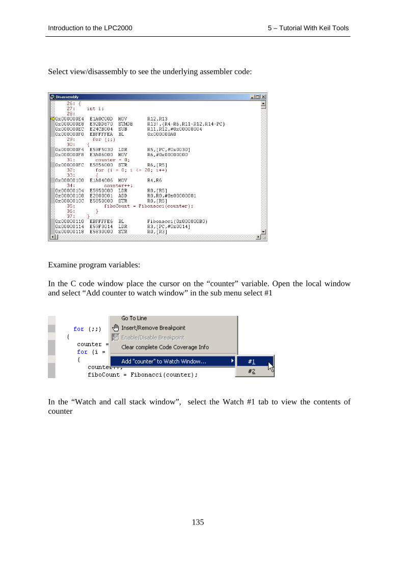
Introduction to the LPC2000 5 – Tutorial With Keil Tools
135
Select view/disassembly to see the underlying assembler code:
Examine program variables: In the C code window place the cursor on the “counter” variable. Open the local window and select “Add counter to watch window” in the sub menu select #1
In the “Watch and call stack window”, select the Watch #1 tab to view the contents of counter
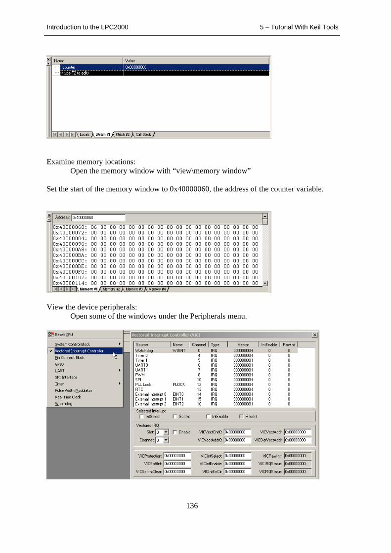
Introduction to the LPC2000 5 – Tutorial With Keil Tools
136
Examine memory locations: Open the memory window with “view\memory window” Set the start of the memory window to 0x40000060, the address of the counter variable.
View the device peripherals: Open some of the windows under the Peripherals menu.

Introduction to the LPC2000 5 – Tutorial With Keil Tools
137
The debugger has many mode functions but the above debugging tools will allow you to run the course exercises. The simulator can also be replaced by a JTAG debugger and the same front end can be used to debug real hardware.
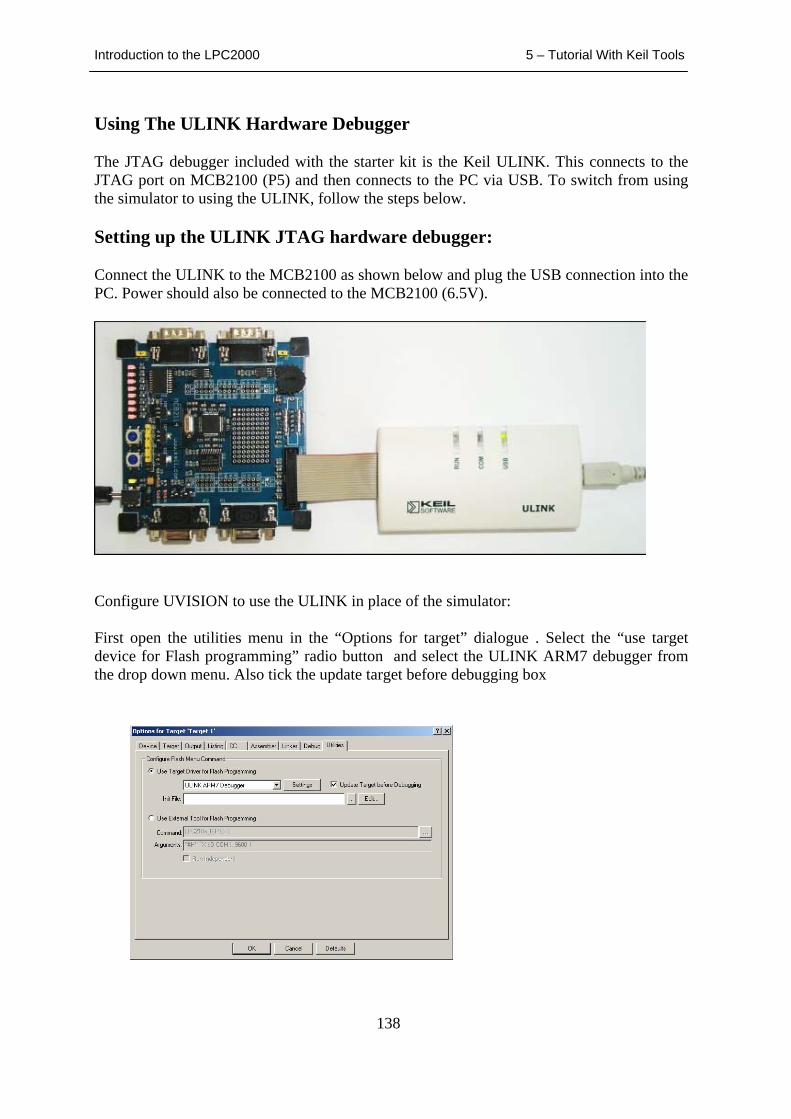
Introduction to the LPC2000 5 – Tutorial With Keil Tools
138
Using The ULINK Hardware Debugger The JTAG debugger included with the starter kit is the Keil ULINK. This connects to the JTAG port on MCB2100 (P5) and then connects to the PC via USB. To switch from using the simulator to using the ULINK, follow the steps below. Setting up the ULINK JTAG hardware debugger: Connect the ULINK to the MCB2100 as shown below and plug the USB connection into the PC. Power should also be connected to the MCB2100 (6.5V).
Configure UVISION to use the ULINK in place of the simulator: First open the utilities menu in the “Options for target” dialogue . Select the “use target device for Flash programming” radio button and select the ULINK ARM7 debugger from the drop down menu. Also tick the update target before debugging box
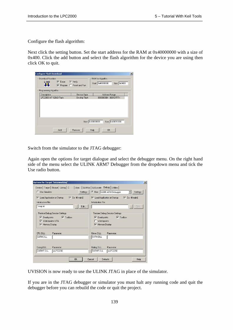
Introduction to the LPC2000 5 – Tutorial With Keil Tools
139
Configure the flash algorithm: Next click the setting button. Set the start address for the RAM at 0x40000000 with a size of 0x400. Click the add button and select the flash algorithm for the device you are using then click OK to quit.
Switch from the simulator to the JTAG debugger: Again open the options for target dialogue and select the debugger menu. On the right hand side of the menu select the ULINK ARM7 Debugger from the dropdown menu and tick the Use radio button.
UVISION is now ready to use the ULINK JTAG in place of the simulator. If you are in the JTAG debugger or simulator you must halt any running code and quit the debugger before you can rebuild the code or quit the project.
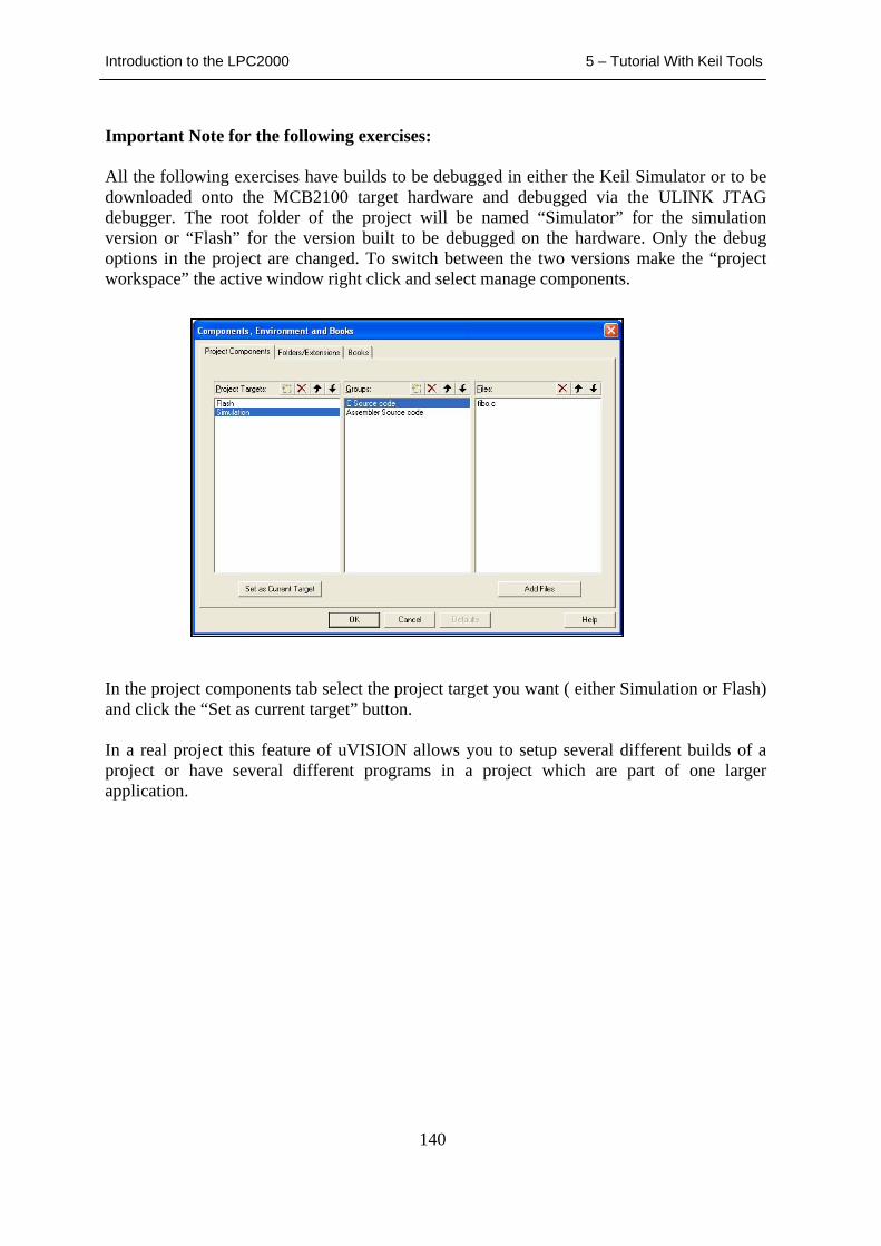
Introduction to the LPC2000 5 – Tutorial With Keil Tools
140
Important Note for the following exercises: All the following exercises have builds to be debugged in either the Keil Simulator or to be downloaded onto the MCB2100 target hardware and debugged via the ULINK JTAG debugger. The root folder of the project will be named “Simulator” for the simulation version or “Flash” for the version built to be debugged on the hardware. Only the debug options in the project are changed. To switch between the two versions make the “project workspace” the active window right click and select manage components.
In the project components tab select the project target you want ( either Simulation or Flash) and click the “Set as current target” button. In a real project this feature of uVISION allows you to setup several different builds of a project or have several different programs in a project which are part of one larger application.
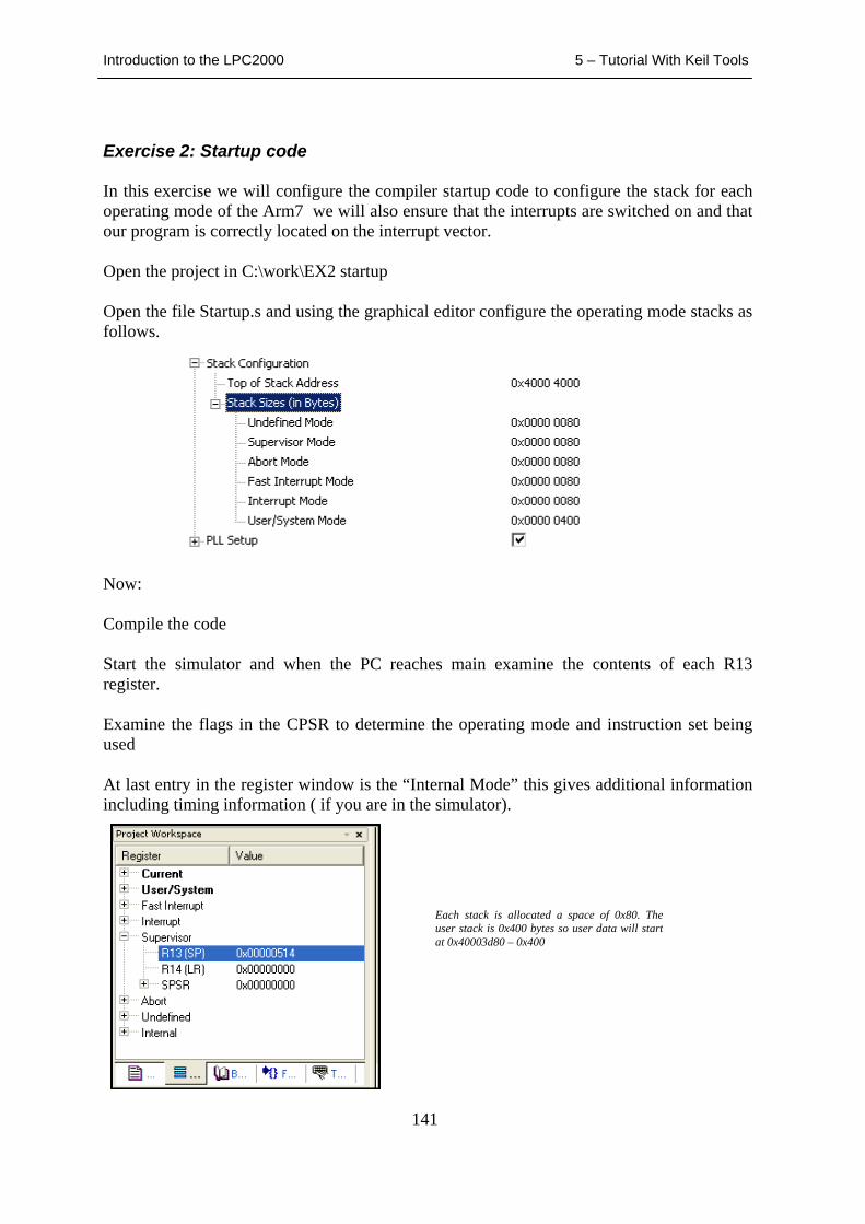
Introduction to the LPC2000 5 – Tutorial With Keil Tools
141
Exercise 2: Startup code In this exercise we will configure the compiler startup code to configure the stack for each operating mode of the Arm7 we will also ensure that the interrupts are switched on and that our program is correctly located on the interrupt vector. Open the project in C:\work\EX2 startup Open the file Startup.s and using the graphical editor configure the operating mode stacks as follows.
Now: Compile the code Start the simulator and when the PC reaches main examine the contents of each R13 register. Examine the flags in the CPSR to determine the operating mode and instruction set being used At last entry in the register window is the “Internal Mode” this gives additional information including timing information ( if you are in the simulator).
Each stack is allocated a space of 0x80. Theuser stack is 0x400 bytes so user data will startat 0x40003d80 – 0x400
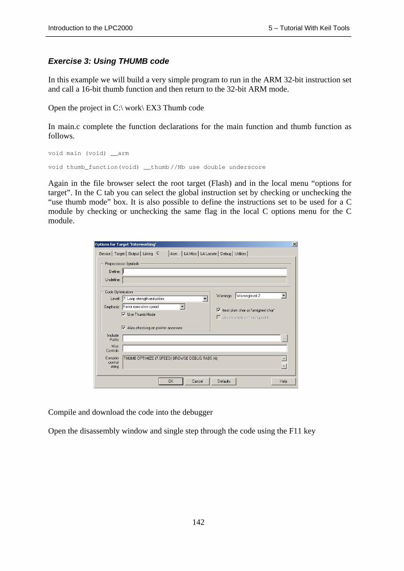
Introduction to the LPC2000 5 – Tutorial With Keil Tools
142
Exercise 3: Using THUMB code In this example we will build a very simple program to run in the ARM 32-bit instruction set and call a 16-bit thumb function and then return to the 32-bit ARM mode. Open the project in C:\ work\ EX3 Thumb code In main.c complete the function declarations for the main function and thumb function as follows. void main (void) __arm void thumb_function(void) __thumb //Nb use double underscore Again in the file browser select the root target (Flash) and in the local menu “options for target”. In the C tab you can select the global instruction set by checking or unchecking the “use thumb mode” box. It is also possible to define the instructions set to be used for a C module by checking or unchecking the same flag in the local C options menu for the C module.
Compile and download the code into the debugger Open the disassembly window and single step through the code using the F11 key
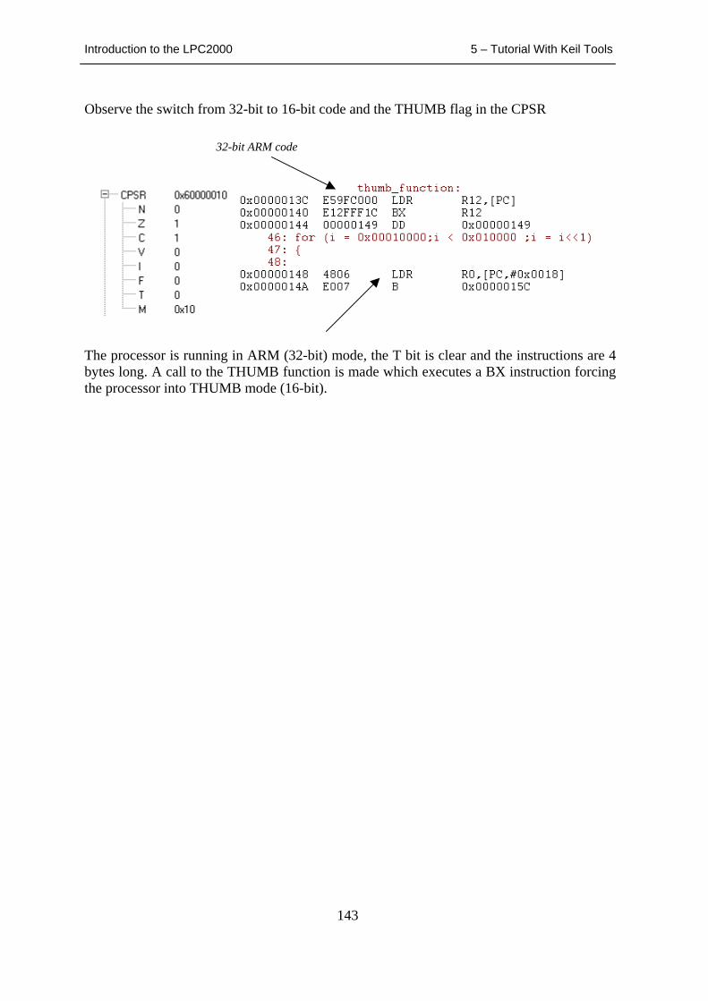
Introduction to the LPC2000 5 – Tutorial With Keil Tools
143
Observe the switch from 32-bit to 16-bit code and the THUMB flag in the CPSR
The processor is running in ARM (32-bit) mode, the T bit is clear and the instructions are 4 bytes long. A call to the THUMB function is made which executes a BX instruction forcing the processor into THUMB mode (16-bit).
32-bit ARM code
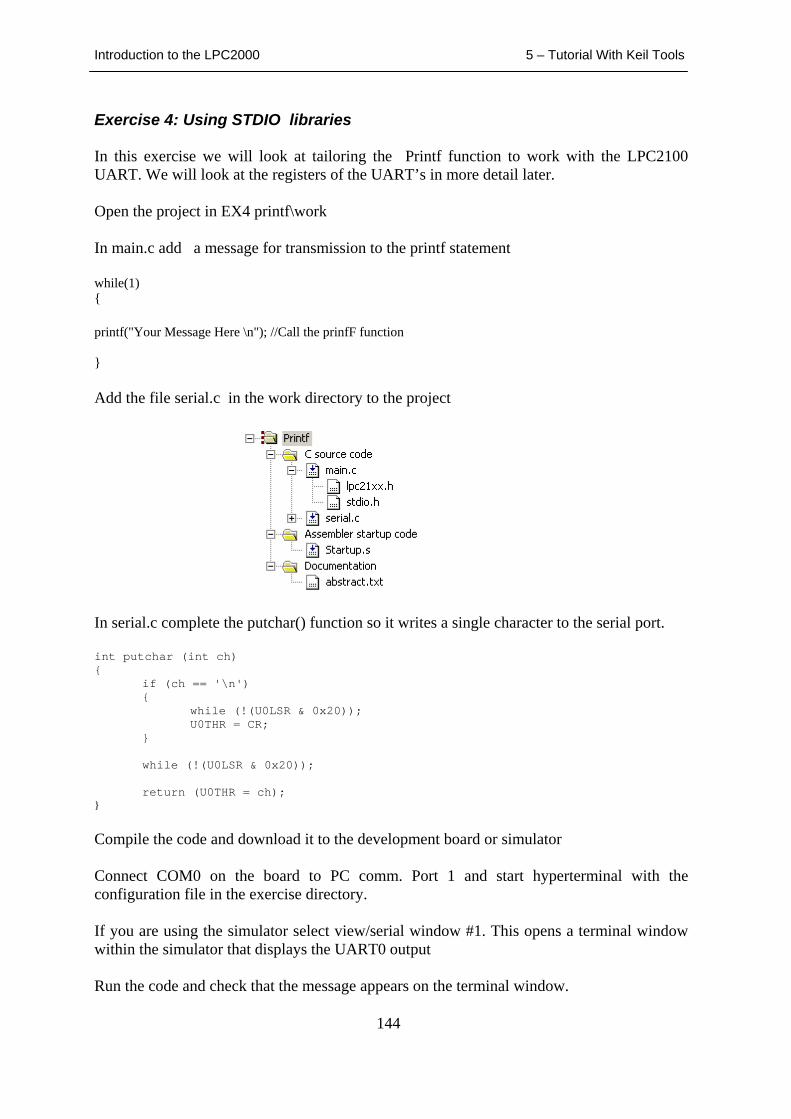
Introduction to the LPC2000 5 – Tutorial With Keil Tools
144
Exercise 4: Using STDIO libraries In this exercise we will look at tailoring the Printf function to work with the LPC2100 UART. We will look at the registers of the UART’s in more detail later. Open the project in EX4 printf\work In main.c add a message for transmission to the printf statement while(1) { printf("Your Message Here \n"); //Call the prinfF function } Add the file serial.c in the work directory to the project
In serial.c complete the putchar() function so it writes a single character to the serial port. int putchar (int ch) {
if (ch == '\n') {
while (!(U0LSR & 0x20)); U0THR = CR;
} while (!(U0LSR & 0x20)); return (U0THR = ch); } Compile the code and download it to the development board or simulator Connect COM0 on the board to PC comm. Port 1 and start hyperterminal with the configuration file in the exercise directory. If you are using the simulator select view/serial window #1. This opens a terminal window within the simulator that displays the UART0 output Run the code and check that the message appears on the terminal window.
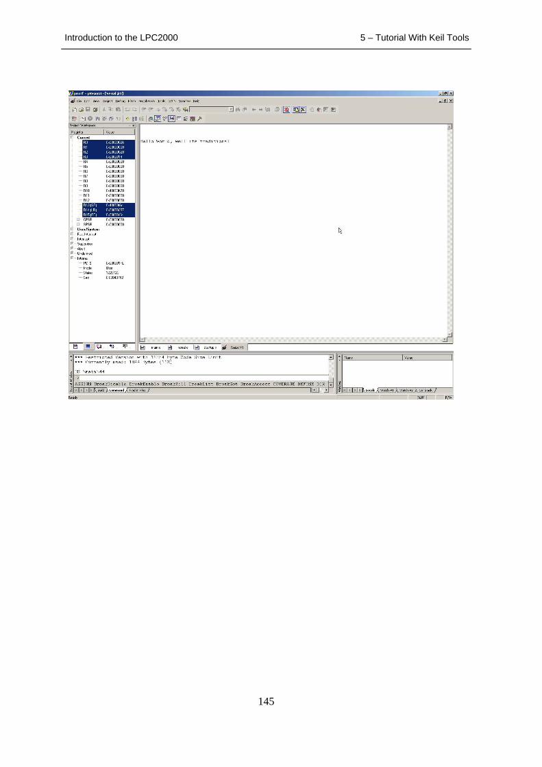
Introduction to the LPC2000 5 – Tutorial With Keil Tools
145
Introduction to the LPC2000 5 – Tutorial With Keil Tools
146
Exercise 5: Simple interrupt In this exercise we will setup a basic FIQ interrupt and see it serviced. Open the project in C:\work\EX5-Interrupt In main.c complete the definition of the FIQ_Handler function to define it as the FIQ interrupt service routine void FIQ_Handler (void) __fiq
In startup.s complete the vector constants table to define EXTintFIQ as the FIQ ISR. __startup PROC CODE32 Vectors: LDR PC,=Reset_Addr LDR PC,Undef_Addr LDR PC,SWI_Addr LDR PC,PAbt_Addr LDR PC,DAbt_Addr NOP /* Reserved Vector */ LDR PC,[PC, #--0x0FF0] LDR PC,FIQ_Addr Reset_Addr: DD Reset_Handler Undef_Addr: DD Undef_Handler SWI_Addr: DD SWI_Handler PAbt_Addr: DD PAbt_Handler DAbt_Addr: DD DAbt_Handler DD 0 /* Reserved Address */ IRQ_Addr: DD IRQ_Handler FIQ_Addr: DD FIQ_Handler?A Compile the code and download it onto the board. Step through the code until you reach the while loop Set a breakpoint in the FIQ_Handler function Press F5 to set the program running On the MCB2100 board press the INT button to generate the interrupt.
The FIQ interrupt vector, the instruction loads the address of the c routine into the PC
The constants table holds the address of the FIQ C routine
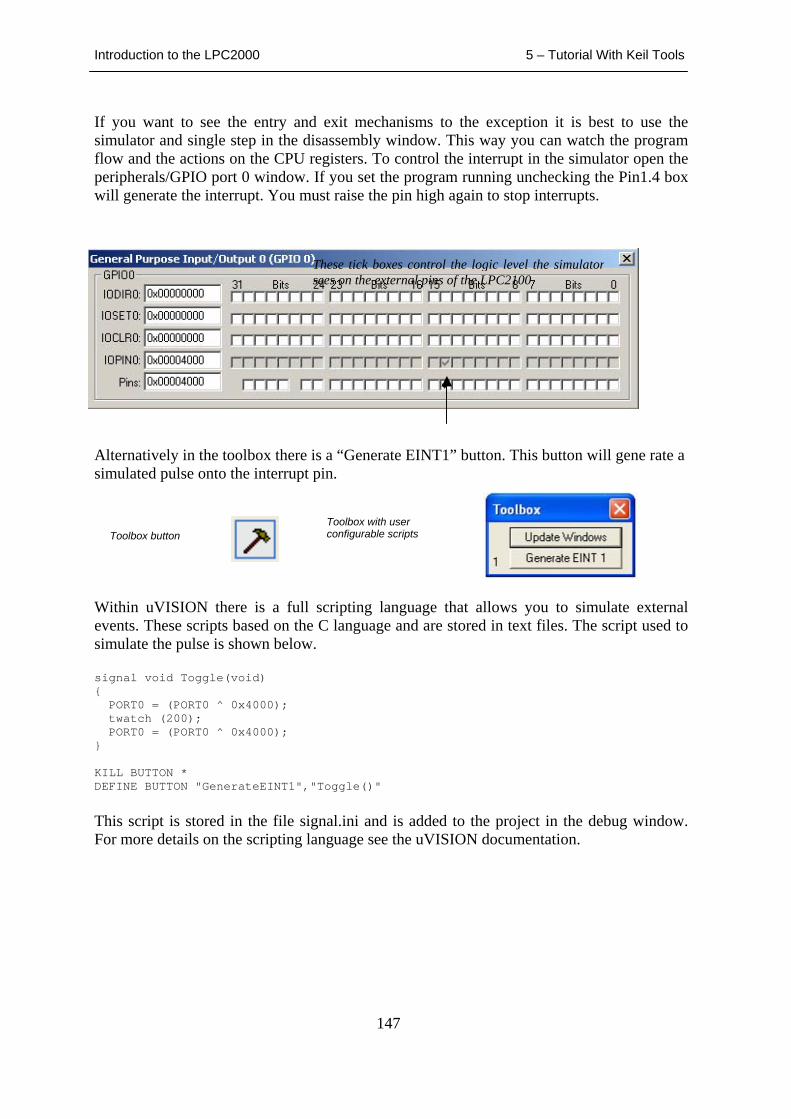
Introduction to the LPC2000 5 – Tutorial With Keil Tools
147
If you want to see the entry and exit mechanisms to the exception it is best to use the simulator and single step in the disassembly window. This way you can watch the program flow and the actions on the CPU registers. To control the interrupt in the simulator open the peripherals/GPIO port 0 window. If you set the program running unchecking the Pin1.4 box will generate the interrupt. You must raise the pin high again to stop interrupts.
Alternatively in the toolbox there is a “Generate EINT1” button. This button will gene rate a simulated pulse onto the interrupt pin.
Within uVISION there is a full scripting language that allows you to simulate external events. These scripts based on the C language and are stored in text files. The script used to simulate the pulse is shown below. signal void Toggle(void) { PORT0 = (PORT0 ^ 0x4000); twatch (200); PORT0 = (PORT0 ^ 0x4000); } KILL BUTTON * DEFINE BUTTON "GenerateEINT1","Toggle()"
This script is stored in the file signal.ini and is added to the project in the debug window. For more details on the scripting language see the uVISION documentation.
These tick boxes control the logic level the simulatorsees on the external pins of the LPC2100
Toolbox button Toolbox with user configurable scripts
Introduction to the LPC2000 5 – Tutorial With Keil Tools
148
Exercise 6: Software Interrupt In this exercise we will define an inline assembler function to call a software interrupt and place the value 0x02 in the calling instruction. In the Software interrupt SWI we will decode the instruction to see which SWI function has been called and then use a case statement to run the appropriate code. Open the project in C:\work\EX6 SWI\ Add the file SWI_VEC.S to the project In Main.c declare the two function as SWI functions as follows void SWI_Call1(int pattern) __swi(8) { … } void SWI_Call2(void) __swi(9) { … }
Compile and download the code into the debugger Step the code and observe the SWI being serviced In the disassembly window we can see the call to the first function. This passes the parameter and generates an SWI which is packed with the integer 8. In the register window we can read the CPSR which shows we are in user mode.
Once we have generated the software interrupt the chip will change modes run the code in vectors.s and then enter our number 8 SWI function .
Branch to function is replaced by answi instruction User mode
Supervisor mode
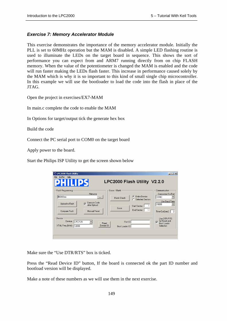
Introduction to the LPC2000 5 – Tutorial With Keil Tools
149
Exercise 7: Memory Accelerator Module This exercise demonstrates the importance of the memory accelerator module. Initially the PLL is set to 60MHz operation but the MAM is disabled. A simple LED flashing routine is used to illuminate the LEDs on the target board in sequence. This shows the sort of performance you can expect from and ARM7 running directly from on chip FLASH memory. When the value of the potentiometer is changed the MAM is enabled and the code will run faster making the LEDs flash faster. This increase in performance caused solely by the MAM which is why it is so important to this kind of small single chip microcontroller. In this example we will use the bootloader to load the code into the flash in place of the JTAG. Open the project in exercises/EX7-MAM In main.c complete the code to enable the MAM In Options for target/output tick the generate hex box Build the code Connect the PC serial port to COM0 on the target board Apply power to the board. Start the Philips ISP Utility to get the screen shown below
Make sure the “Use DTR/RTS” box is ticked. Press the “Read Device ID” button, If the board is connected ok the part ID number and bootload version will be displayed. Make a note of these numbers as we will use them in the next exercise.
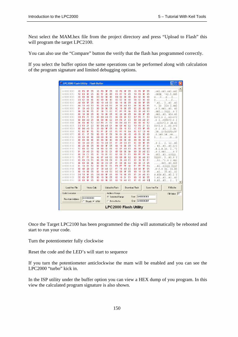
Introduction to the LPC2000 5 – Tutorial With Keil Tools
150
Next select the MAM.hex file from the project directory and press “Upload to Flash” this will program the target LPC2100. You can also use the “Compare” button the verify that the flash has programmed correctly. If you select the buffer option the same operations can be performed along with calculation of the program signature and limited debugging options.
Once the Target LPC2100 has been programmed the chip will automatically be rebooted and start to run your code. Turn the potentiometer fully clockwise Reset the code and the LED’s will start to sequence If you turn the potentiometer anticlockwise the mam will be enabled and you can see the LPC2000 “turbo” kick in. In the ISP utility under the buffer option you can view a HEX dump of you program. In this view the calculated program signature is also shown.

Introduction to the LPC2000 5 – Tutorial With Keil Tools
151
If you reconnect the JTAG and start the debugger without downloading the program you can examine the interrupt vector table. As we have programmed the flash with the Philips ISP tool the program signature has been added in location 0x00000014 which exists as a NOP in the startup code.
Introduction to the LPC2000 5 – Tutorial With Keil Tools
152
Exercise 8: In-Application programming This example demonstrates how to call the bootloader API from within your application programs. The code makes a call into the bootloader functions to run the “Read\Part ID” function. This example has only been built to work with the MCB2100 evaluation board. Open the project in C:\work\ EX8 IAP Add the following lines of code to main.c command[0] = 0x36; iap(command,result,0x7FFFFFF0);
Add the following lines to API.c #pragma asm mov r15,r2; //move entry address into PC #pragma endasm
Now make sure that main is compiled as ARM code and API is built as Thumb code Build the code and start the debugger Run the code up to the first call to the IAP function. Set a breakpoint on the line of code after this function Step into the IAP function Look at the contents of R0-R2, These registers should contain the addresses of the command table, the results table and the entry address of the bootloader functions. Also R14 should contain the return address to the main function. Step the line of assembly code which will jump you to 0x7FFFFFFF. This is the entry to the bootloader code. Now run the code at full speed, it will execute the bootloader function called and return to the address held in R14 ( the next line in main.c). When the code hits the breakpoint examine the CPSR to see which instruction set is now being used. Take a look at the result table and read the PartID number returned by the bootloader. Compare this to the value returned in the previous example. Run the next call to the Bootloader API and check that the correct bootloader version is returned.
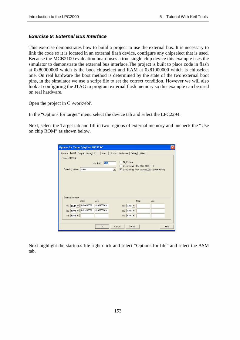
Introduction to the LPC2000 5 – Tutorial With Keil Tools
153
Exercise 9: External Bus Interface This exercise demonstrates how to build a project to use the external bus. It is necessary to link the code so it is located in an external flash device, configure any chipselect that is used. Because the MCB2100 evaluation board uses a true single chip device this example uses the simulator to demonstrate the external bus interface.The project is built to place code in flash at 0x80000000 which is the boot chipselect and RAM at 0x81000000 which is chipselect one. On real hardware the boot method is determined by the state of the two external boot pins, in the simulator we use a script file to set the correct condition. However we will also look at configuring the JTAG to program external flash memory so this example can be used on real hardware. Open the project in C:\work\ebi\ In the “Options for target” menu select the device tab and select the LPC2294. Next, select the Target tab and fill in two regions of external memory and uncheck the “Use on chip ROM” as shown below.
Next highlight the startup.s file right click and select “Options for file” and select the ASM tab.
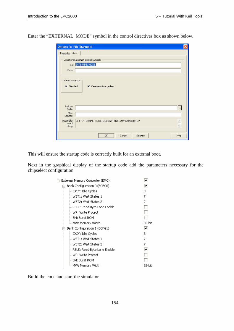
Introduction to the LPC2000 5 – Tutorial With Keil Tools
154
Enter the “EXTERNAL_MODE” symbol in the control directives box as shown below.
This will ensure the startup code is correctly built for an external boot. Next in the graphical display of the startup code add the parameters necessary for the chipselect configuration
Build the code and start the simulator
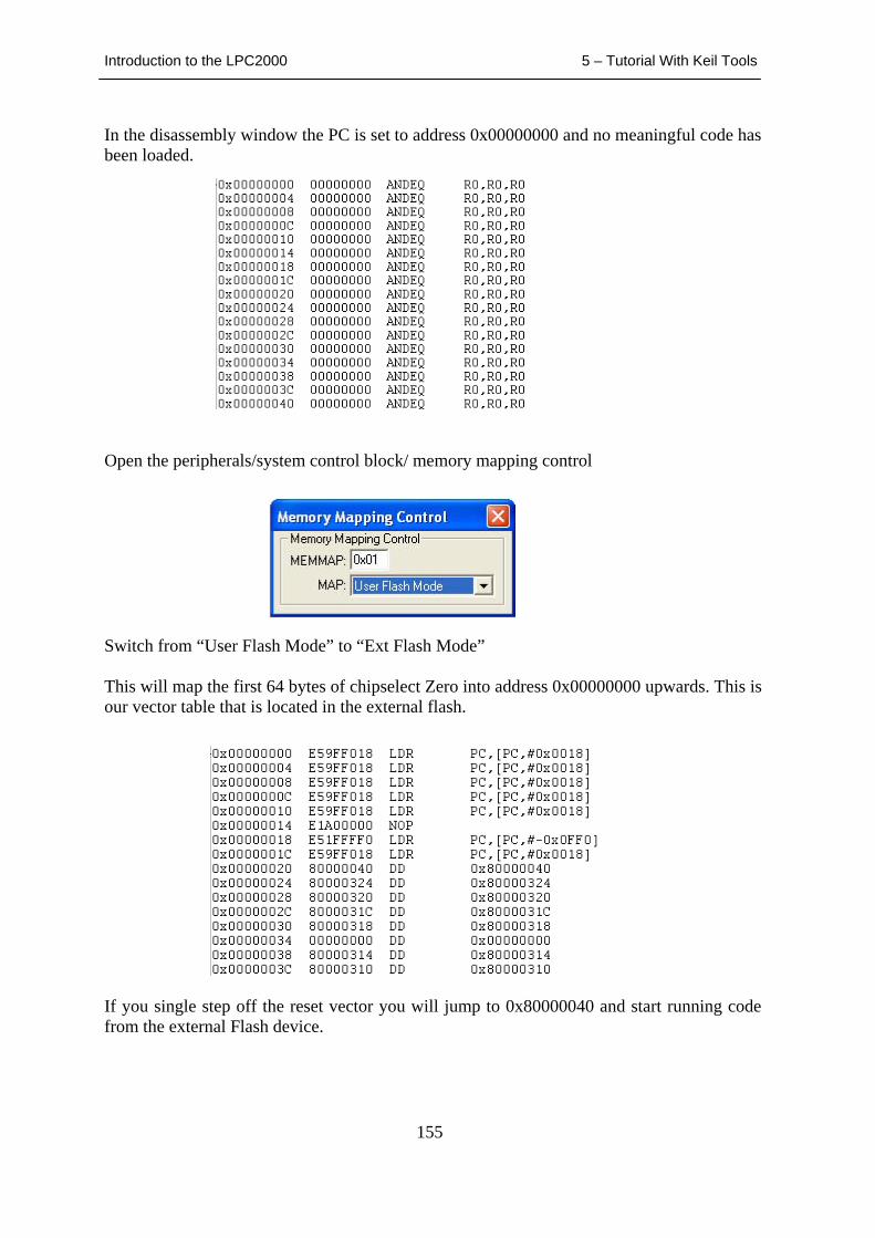
Introduction to the LPC2000 5 – Tutorial With Keil Tools
155
In the disassembly window the PC is set to address 0x00000000 and no meaningful code has been loaded.
Open the peripherals/system control block/ memory mapping control
Switch from “User Flash Mode” to “Ext Flash Mode” This will map the first 64 bytes of chipselect Zero into address 0x00000000 upwards. This is our vector table that is located in the external flash.
If you single step off the reset vector you will jump to 0x80000040 and start running code from the external Flash device.
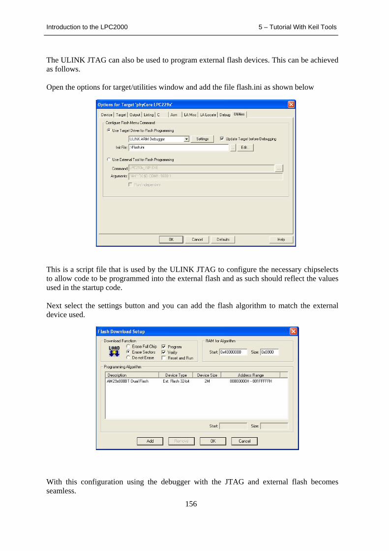
Introduction to the LPC2000 5 – Tutorial With Keil Tools
156
The ULINK JTAG can also be used to program external flash devices. This can be achieved as follows. Open the options for target/utilities window and add the file flash.ini as shown below
This is a script file that is used by the ULINK JTAG to configure the necessary chipselects to allow code to be programmed into the external flash and as such should reflect the values used in the startup code. Next select the settings button and you can add the flash algorithm to match the external device used.
With this configuration using the debugger with the JTAG and external flash becomes seamless.
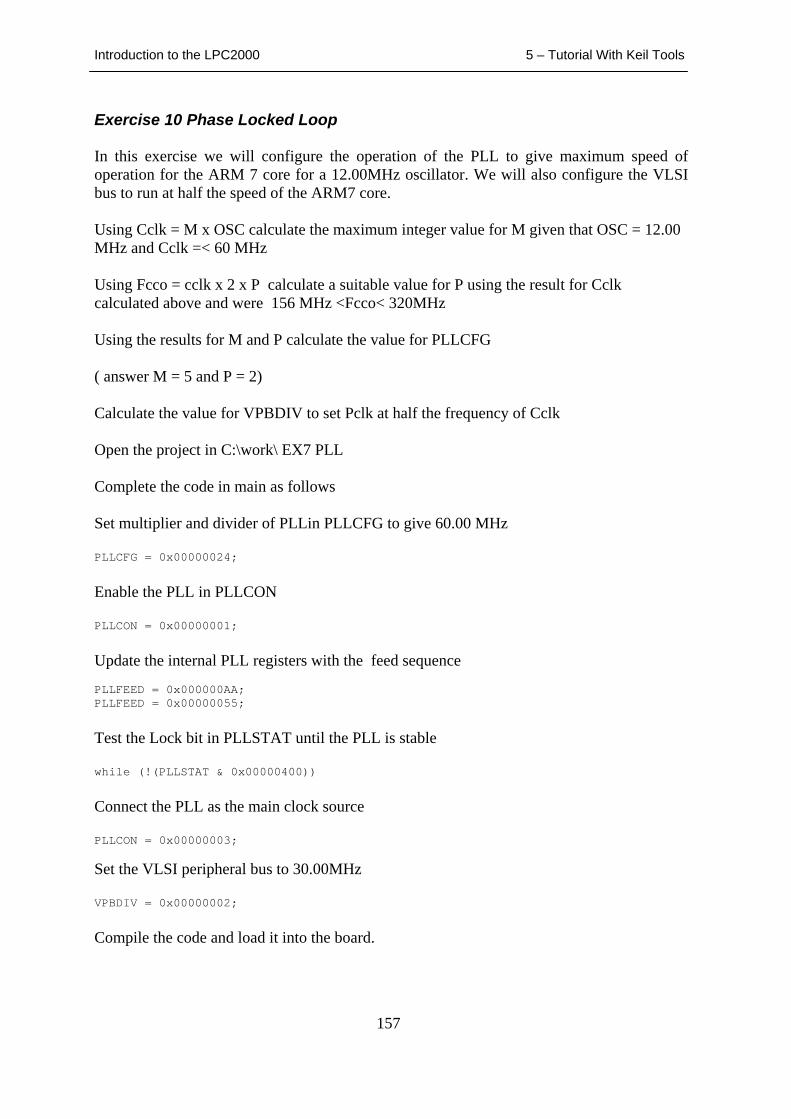
Introduction to the LPC2000 5 – Tutorial With Keil Tools
157
Exercise 10 Phase Locked Loop In this exercise we will configure the operation of the PLL to give maximum speed of operation for the ARM 7 core for a 12.00MHz oscillator. We will also configure the VLSI bus to run at half the speed of the ARM7 core. Using Cclk = M x OSC calculate the maximum integer value for M given that OSC = 12.00 MHz and Cclk =< 60 MHz Using Fcco = cclk x 2 x P calculate a suitable value for P using the result for Cclk calculated above and were 156 MHz <Fcco< 320MHz Using the results for M and P calculate the value for PLLCFG ( answer M = 5 and P = 2) Calculate the value for VPBDIV to set Pclk at half the frequency of Cclk Open the project in C:\work\ EX7 PLL Complete the code in main as follows Set multiplier and divider of PLLin PLLCFG to give 60.00 MHz PLLCFG = 0x00000024;
Enable the PLL in PLLCON PLLCON = 0x00000001;
Update the internal PLL registers with the feed sequence PLLFEED = 0x000000AA; PLLFEED = 0x00000055;
Test the Lock bit in PLLSTAT until the PLL is stable while (!(PLLSTAT & 0x00000400))
Connect the PLL as the main clock source PLLCON = 0x00000003; Set the VLSI peripheral bus to 30.00MHz VPBDIV = 0x00000002;
Compile the code and load it into the board.
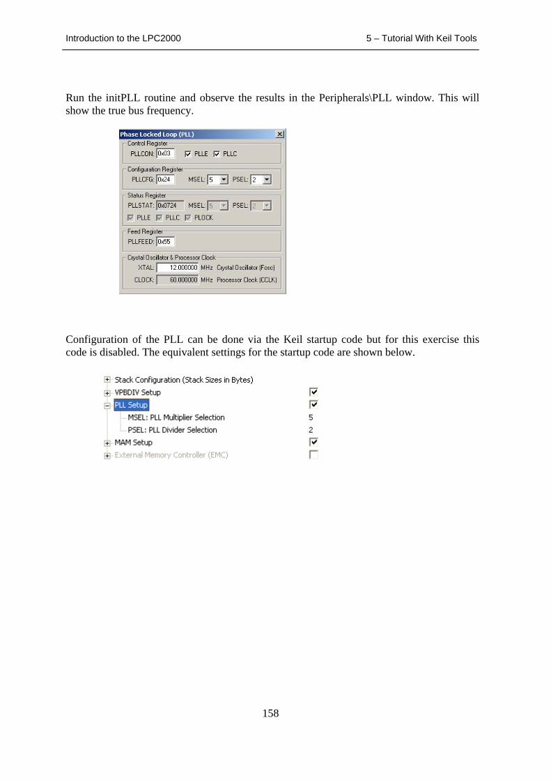
Introduction to the LPC2000 5 – Tutorial With Keil Tools
158
Run the initPLL routine and observe the results in the Peripherals\PLL window. This will show the true bus frequency.
Configuration of the PLL can be done via the Keil startup code but for this exercise this code is disabled. The equivalent settings for the startup code are shown below.
Introduction to the LPC2000 5 – Tutorial With Keil Tools
159
Exercise 11: Fast Interrupt In this exercise we will configure an the external interrupt to be handled as an FIQ. This code was used in exercise 5 to show the C handling of an interrupt function. This time we will see how to configure the hardware for an FIQ interrupt. Open the project in EX12 Interrupt vectored\work Configure the external interrupt as an FIQ by programming the IntSelect register VICIntSelect = 0x00008000;
Compile the code and start the debugger and check the interrupt works as in exercise 5. The name of the FIQ ISR must match the name in the vector constant table in startup.s. The default name given by Keil is FIQ_Handler. If you are using the simulator the interrupt can be triggered by setting pin 0.14 low in the peripherals/GPIO window or by using the “Generate EINT1” button in the toolbox
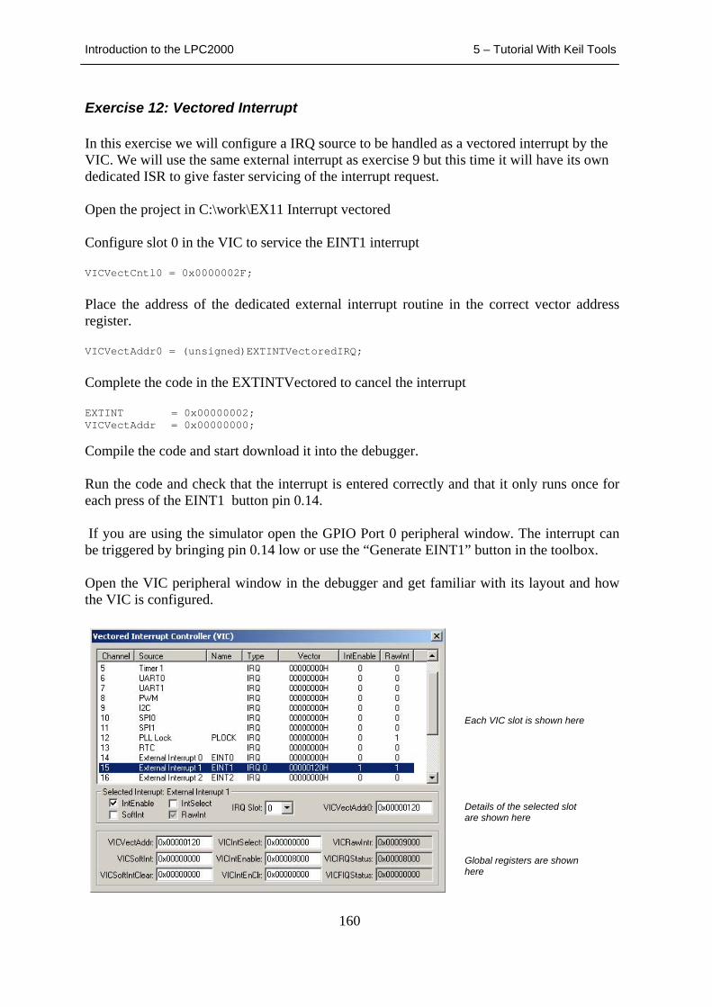
Introduction to the LPC2000 5 – Tutorial With Keil Tools
160
Exercise 12: Vectored Interrupt In this exercise we will configure a IRQ source to be handled as a vectored interrupt by the VIC. We will use the same external interrupt as exercise 9 but this time it will have its own dedicated ISR to give faster servicing of the interrupt request. Open the project in C:\work\EX11 Interrupt vectored Configure slot 0 in the VIC to service the EINT1 interrupt VICVectCntl0 = 0x0000002F;
Place the address of the dedicated external interrupt routine in the correct vector address register. VICVectAddr0 = (unsigned)EXTINTVectoredIRQ;
Complete the code in the EXTINTVectored to cancel the interrupt EXTINT = 0x00000002; VICVectAddr = 0x00000000; Compile the code and start download it into the debugger. Run the code and check that the interrupt is entered correctly and that it only runs once for each press of the EINT1 button pin 0.14. If you are using the simulator open the GPIO Port 0 peripheral window. The interrupt can be triggered by bringing pin 0.14 low or use the “Generate EINT1” button in the toolbox. Open the VIC peripheral window in the debugger and get familiar with its layout and how the VIC is configured.
Each VIC slot is shown here
Details of the selected slot are shown here
Global registers are shown here

Introduction to the LPC2000 5 – Tutorial With Keil Tools
161
In the simulator use the cycle counter in the register window calculate how long the device takes to enter to the first line of your code in the interrupt routine
Introduction to the LPC2000 5 – Tutorial With Keil Tools
162
Exercise 13 : Non Vectored Interrupt In this exercise we will use the Vector interrupt unit to generate the slowest form of interrupt response a non vectored interrupt . We will use External interrupt one EINT1 to generate an interrupt. The VIC will respond to this interrupt event by providing the address of a general purpose ISR for the processor to jump to. On entry to this routine the ISR must calculate the source of the interrupt, take appropriate action and then correctly exit the ISR and resume normal processing. Open the project in EX9-Interrupt Non Vectored\work In Startup.s add the correct assembly code to the IRQ interrupt vector LDR PC,[PC, #-0xFF0]
In main.c configure the Pin Connect Block to enable P0.14 as an External interrupt. PINSEL0 = 0x20000000;
Place the address of the NonVectored ISR into the Default vector address register. Note in C this can be done as follows: VICDefVectAddr = (unsigned)<Name of ISR routine>;
Enable the External interrupt channel in the VIC VICIntEnable = 0x8000;
In the interrupt routine check the IRQ status register to find the source of the interrupt if(VICIRQStatus&0x00008000)
At the end of the ISR clear the interrupt flag in EINT0 register and perform dummy write to the correct register in the VIC to clear the interrupt source EXTINT = 0x00000002;
VICVectAddr = 0x00000000;
Compile the code and start the debugger Run the code and check that the interrupt is entered correctly and that it only runs once for each press of the EINT1 button pin 0.14. If you are using the simulator open the GPIO Port 0 peripheral window. The interrupt can be triggered by bringing pin 0.14 low. Alternatively open the toolbox and use the “Generate EINT1” button. In the simulator use the cycle counter in the register window calculate how long the device takes to enter to the first line of your code in the interrupt routine
Introduction to the LPC2000 5 – Tutorial With Keil Tools
163
Exercise 14: Nested Interrupts In this exercise we will setup two interrupt sources. First timer0 which sets a port pin high for the duration of the interrupt and secondly external interrupt one which also sets a second port pin high for the duration of the interrupt. Under normal operation both interrupts would block each other while they are running. However by adding the appropriate macros to the External interrupt routine we can allow the timer interrupt to interrupt the external interrupt routine so it will be guaranteed to run every 10ms. This can be observed on the LEDS on theMCB2100 or in the logic analyser of the simulator. Open the project in EX14-Interrupt Non Vectored\work In Main.c complete the two IENABLE and IDISABLE macros #define IENABLE // Nested Interrupts Entry __asm { MRS LR, SPSR } // Copy SPSR_irq to LR __asm { STMFD SP!, {LR} } // Save SPSR_irq __asm { MSR CPSR_c, #0x1F } // Enable IRQ (Sys Mode) __asm { STMFD SP!, {LR} } // Save LR #define IDISABLE // Nested Interrupts Exit __asm { LDMFD SP!, {LR} } // Restore LR __asm { MSR CPSR_c, #0x92 } // Disable IRQ (IRQ Mode) __asm { LDMFD SP!, {LR} } // Restore SPSR_irq to LR __asm { MSR SPSR_cxsf, LR } // Copy LR to SPSR_irq
Add the two macros to the External interrupt service routine void EXINT1_ISR (void) __irq { EXTINT = 2; // Clear EINT1 interrupt flag IENABLE; // allow nested interrupts IOSET1 = 0x00010000; // Switch on an LED delay (0x500000); // wait a long time IOCLR1 = 0x00010000; // Switch off the LED IDISABLE; // disable interrupt nesting VICVectAddr = 0; // Acknowledge Interrupt } Build the project and download it to the debugger If you are using the MCB2100 run the code at full speed. One LED will flash for the period it is in the timer interrupt. Press the INT1 button and the second led will illuminate for the longer period it is in the External interrupt routine. However the timer led will continue to flash because the interrupt is not blocked. If you are using the simulator the same behaviour can be observed using the logic analyser. Remove the IDISABLE and IENABLE macros and observe the new behaviour.
Introduction to the LPC2000 5 – Tutorial With Keil Tools
164
Exercise 15: General purpose IO pins In this exercise we will use the GPIO pins. A group of pins will be set as outputs and then each will be flashed sequentially. Open the project in EX12 GPIO\work Add the include file for the LPC21xx SFR’s #include <LPC21xx.H>
Program the data direction register to enable pins 1.16 – 1.23 as output IODIR1 = 0x00FF0000;
Complete the ChangeGPIOPinState function to clear and set the relevant pins IOCLR1 = ~state; IOSET1 = state;
Compile the code and download it into the debugger Run the code on the MCB2100 to see the LED chaser. If you are using the simulator step through the code and check it works by examining the state of the IO pins via the GPIO peripheral window
Introduction to the LPC2000 5 – Tutorial With Keil Tools
165
Exercise 16: Timer Capture In this exercise we will use timer 0 in a simple compare mode to measure the time between starting the timer and getting a rising edge on pin 0.02. Because the MCB2100 does not have a button on a capture channel to generate the pulse this exercise is based on the Simulator. A target version is included but you would need to modify the MCB2100 hardware and observe the output on an oscilloscope. Pclk = 30 MHz Pclock tick = 0.033MHz
Open the project in EX18 Timer capture\work In main.c complete the code as follows Enable pin 0.2 as capture channel 0: PINSEL0 = 0x00000020; Load prescaler with 1 micro second tick value: T0PR = 0x0000001E; Reset timer counter and prescaler counter registers: T0TCR = 0x00000002; Configure capture channel 0 to capture on the rising edge: T0CCR = 0x00000005; Enable the timer: T0TCR = 0x00000001; In the interrupt routine copy the capture value into a dummy variable: Value = T0CR0; Compile and load the code into the debugger Run the program and check the following Test the capture interrupt is working by setting a breakpoint on the timer ISR, and running the code. In the simulator a script has been added to the toolbox to generate a pulse on 0.02. If you are using the MCB2100 you need to pull the port pin up to Vcc via a 10K resistor.
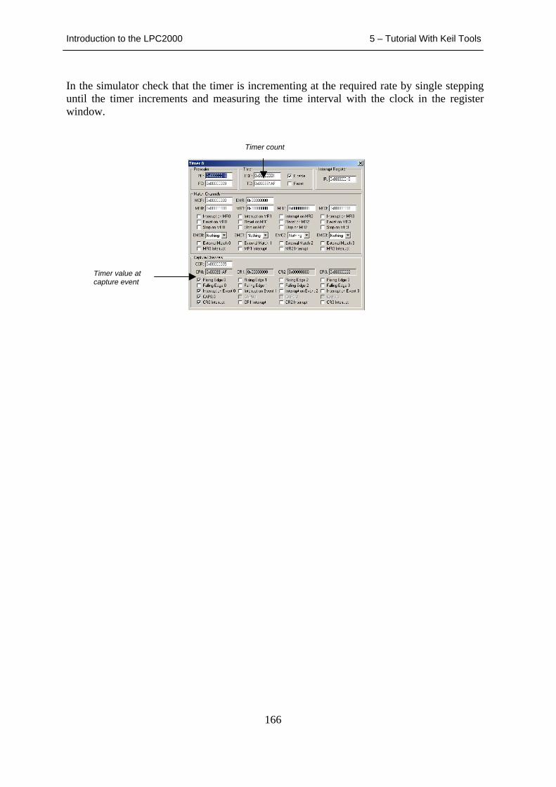
Introduction to the LPC2000 5 – Tutorial With Keil Tools
166
In the simulator check that the timer is incrementing at the required rate by single stepping until the timer increments and measuring the time interval with the clock in the register window.
Timer value at capture event
Timer count
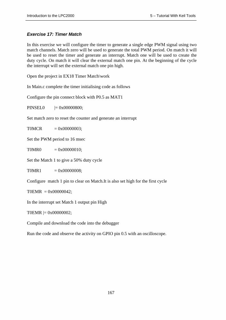
Introduction to the LPC2000 5 – Tutorial With Keil Tools
167
Exercise 17: Timer Match In this exercise we will configure the timer to generate a single edge PWM signal using two match channels. Match zero will be used to generate the total PWM period. On match it will be used to reset the timer and generate an interrupt. Match one will be used to create the duty cycle. On match it will clear the external match one pin. At the beginning of the cycle the interrupt will set the external match one pin high. Open the project in EX18 Timer Match\work In Main.c complete the timer initialising code as follows Configure the pin connect block with P0.5 as MAT1 PINSEL0 |= 0x00000800; Set match zero to reset the counter and generate an interrupt T0MCR = 0x00000003; Set the PWM period to 16 msec T0MR0 = 0x00000010; Set the Match 1 to give a 50% duty cycle T0MR1 = 0x00000008; Configure match 1 pin to clear on Match.It is also set high for the first cycle T0EMR = 0x00000042; In the interrupt set Match 1 output pin High T0EMR |= 0x00000002; Compile and download the code into the debugger Run the code and observe the activity on GPIO pin 0.5 with an oscilloscope.
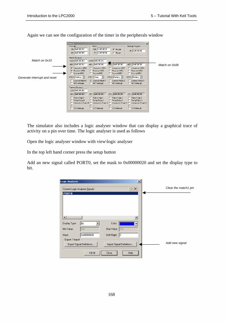
Introduction to the LPC2000 5 – Tutorial With Keil Tools
168
Again we can see the configuration of the timer in the peripherals window
The simulator also includes a logic analyser window that can display a graphical trace of activity on a pin over time. The logic analyser is used as follows Open the logic analyser window with view\logic analyser In the top left hand corner press the setup button Add an new signal called PORT0, set the mask to 0x00000020 and set the display type to bit.
Match on 0x10 Match on 0x08
Generate interrupt and reset
Clear the match1 pin
Add new signal
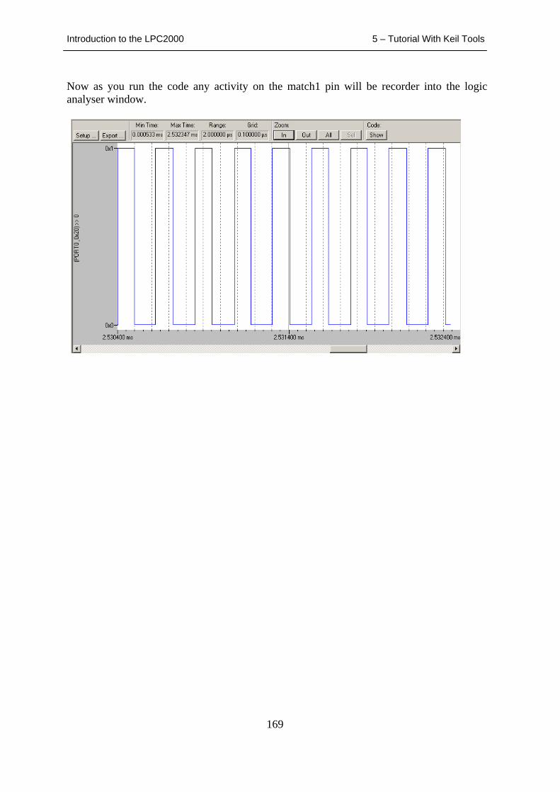
Introduction to the LPC2000 5 – Tutorial With Keil Tools
169
Now as you run the code any activity on the match1 pin will be recorder into the logic analyser window.
Introduction to the LPC2000 5 – Tutorial With Keil Tools
170
Exercise 18: Dual-Edge (Symmetrical) PWM Generation. In this exercise we will use the PWM module to generate a single channel of symmetrically modulated PWM signal. This will use the MAT0 channel to generate to total signal period and will be configured to reset the timer. MAT1 will be user to generate the turn on off and MAT2 will generate the turn off point. The PWM duty cycle can then be modulated by the +- keys in serial window 2. Open the project in C:\work\ EX20 PWMModule In main.c complete the code as follows Enable pin 0.7 as PWM2 PINSEL0 |= 0x00008000; Configure PWM channel two to double edge control, output enabled PWMPCR = 0x0000404; Configure Timer 0 reset to the counter PWMMCR = 0x00000003; Set the reload values of mat1 and mat2 to give an initial “spike” which is gradually broadened in the main loop as the code runs. PWMMR0 = 0x000000FF; PWMMR1 = 0x00000080; PWMMR2 = 0x00000080; enable shadow latch for match 0 - 2 PWMLER = 0x00000007; Reset counter and prescaler and enable PWM mode PWMTCR = 0x00000002; enable timer with PWM enabled PWMTCR = 0x00000009; In the main while loop enable the shadow latch to update the match registers when a new values are available. PWMLER = 0x0000006;
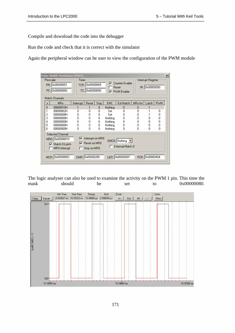
Introduction to the LPC2000 5 – Tutorial With Keil Tools
171
Compile and download the code into the debugger Run the code and check that it is correct with the simulator Again the peripheral window can be user to view the configuration of the PWM module
The logic analyser can also be used to examine the activity on the PWM 1 pin. This time the mask should be set to 0x00000080.
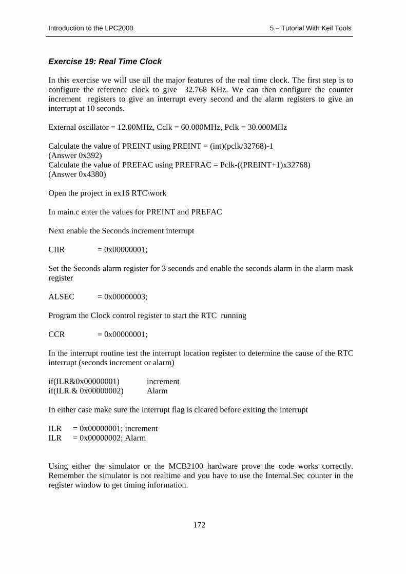
Introduction to the LPC2000 5 – Tutorial With Keil Tools
172
Exercise 19: Real Time Clock In this exercise we will use all the major features of the real time clock. The first step is to configure the reference clock to give 32.768 KHz. We can then configure the counter increment registers to give an interrupt every second and the alarm registers to give an interrupt at 10 seconds. External oscillator = 12.00MHz, Cclk = 60.000MHz, Pclk = 30.000MHz Calculate the value of PREINT using PREINT = (int)(pclk/32768)-1 (Answer 0x392) Calculate the value of PREFAC using PREFRAC = Pclk-((PREINT+1)x32768) (Answer 0x4380) Open the project in ex16 RTC\work In main.c enter the values for PREINT and PREFAC Next enable the Seconds increment interrupt CIIR = 0x00000001; Set the Seconds alarm register for 3 seconds and enable the seconds alarm in the alarm mask register ALSEC = 0x00000003; Program the Clock control register to start the RTC running CCR = 0x00000001; In the interrupt routine test the interrupt location register to determine the cause of the RTC interrupt (seconds increment or alarm) if(ILR&0x00000001) increment if(ILR & 0x00000002) Alarm In either case make sure the interrupt flag is cleared before exiting the interrupt ILR = 0x00000001; increment ILR = 0x00000002; Alarm Using either the simulator or the MCB2100 hardware prove the code works correctly. Remember the simulator is not realtime and you have to use the Internal.Sec counter in the register window to get timing information.
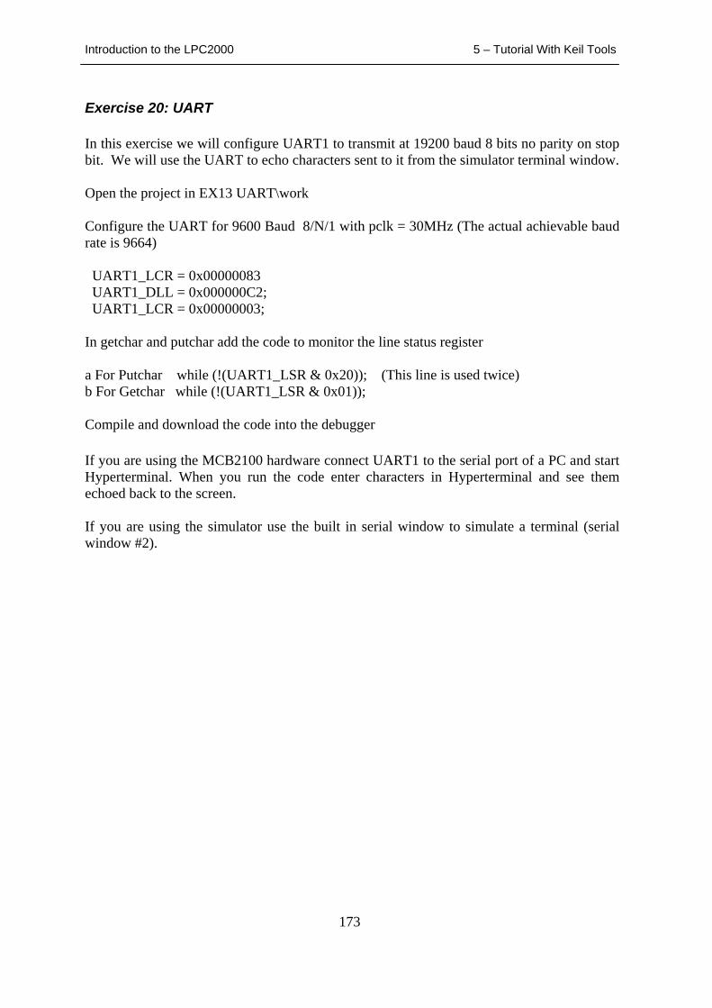
Introduction to the LPC2000 5 – Tutorial With Keil Tools
173
Exercise 20: UART In this exercise we will configure UART1 to transmit at 19200 baud 8 bits no parity on stop bit. We will use the UART to echo characters sent to it from the simulator terminal window. Open the project in EX13 UART\work Configure the UART for 9600 Baud 8/N/1 with pclk = 30MHz (The actual achievable baud rate is 9664) UART1_LCR = 0x00000083 UART1_DLL = 0x000000C2; UART1_LCR = 0x00000003; In getchar and putchar add the code to monitor the line status register a For Putchar while (!(UART1_LSR & 0x20)); (This line is used twice) b For Getchar while (!(UART1_LSR & 0x01)); Compile and download the code into the debugger If you are using the MCB2100 hardware connect UART1 to the serial port of a PC and start Hyperterminal. When you run the code enter characters in Hyperterminal and see them echoed back to the screen. If you are using the simulator use the built in serial window to simulate a terminal (serial window #2).
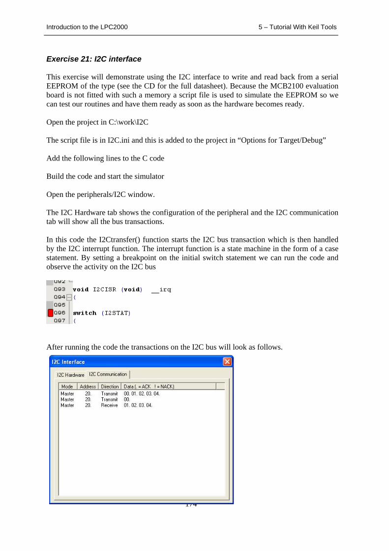
Introduction to the LPC2000 5 – Tutorial With Keil Tools
174
Exercise 21: I2C interface This exercise will demonstrate using the I2C interface to write and read back from a serial EEPROM of the type (see the CD for the full datasheet). Because the MCB2100 evaluation board is not fitted with such a memory a script file is used to simulate the EEPROM so we can test our routines and have them ready as soon as the hardware becomes ready. Open the project in C:\work\I2C The script file is in I2C.ini and this is added to the project in “Options for Target/Debug” Add the following lines to the C code Build the code and start the simulator Open the peripherals/I2C window. The I2C Hardware tab shows the configuration of the peripheral and the I2C communication tab will show all the bus transactions. In this code the I2Ctransfer() function starts the I2C bus transaction which is then handled by the I2C interrupt function. The interrupt function is a state machine in the form of a case statement. By setting a breakpoint on the initial switch statement we can run the code and observe the activity on the I2C bus
After running the code the transactions on the I2C bus will look as follows.
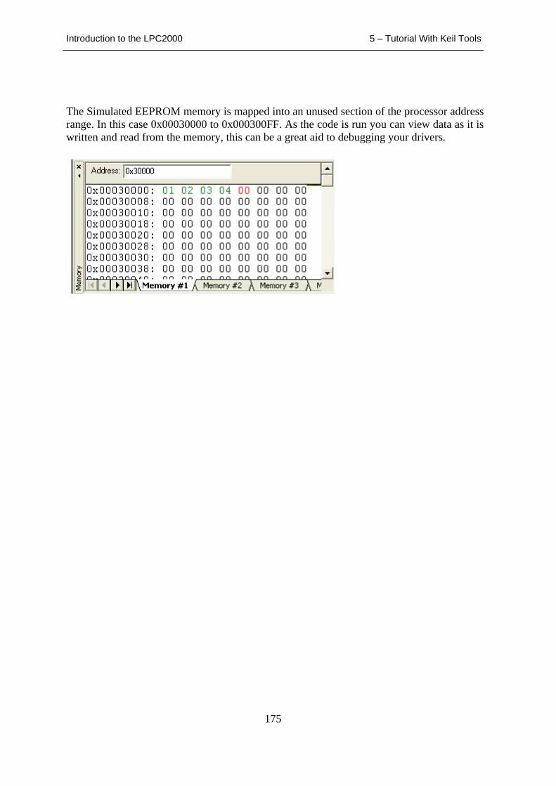
Introduction to the LPC2000 5 – Tutorial With Keil Tools
175
The Simulated EEPROM memory is mapped into an unused section of the processor address range. In this case 0x00030000 to 0x000300FF. As the code is run you can view data as it is written and read from the memory, this can be a great aid to debugging your drivers.
Introduction to the LPC2000 5 – Tutorial With Keil Tools
176
Exercise 22: SPI Like the I2C example this example uses the SPI interface to communicate to a serial EEPROM and demonstrates how to write and read data to such a device. Since the MCB2100 is not fitted with such a memory this example uses the simulator with a script file to simulate the EEPROM. Open the project in C:\work\EX16-SPI The script file is in SPI.ini and this is added to the project in “Options for Target/Debug” The script maps some memory for the SPI EEPROM at 0x700000-0x7000FF In Main.c add the following lines of Code Configure the operation mode and bit timing. S0SPCCR = 0x000000FF; S0SPCR = 0x000000A0;
Kick off an SPI transfer SPI_write(output_buffer,8);
Use a case statement for each state of the transaction case (0x01): //Send Write opcode
S0SPDR = 0x00000005; status = 0x02; //set next state
break; Compile the code and start the simulator Set a breakpoint on the switch statement in the SPI ISR Run the code and examine the state of the virtual EEPROM memory and the debug output in the message window.
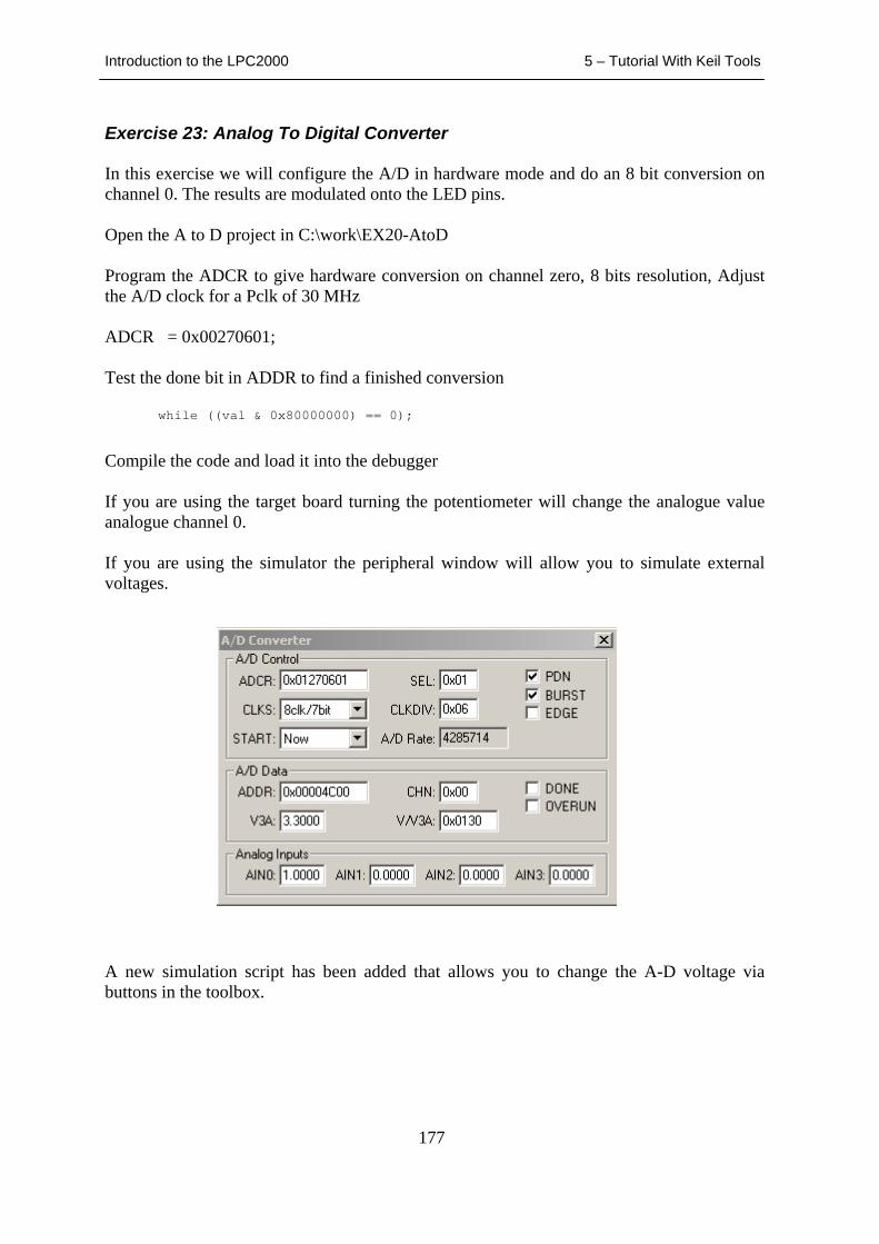
Introduction to the LPC2000 5 – Tutorial With Keil Tools
177
Exercise 23: Analog To Digital Converter In this exercise we will configure the A/D in hardware mode and do an 8 bit conversion on channel 0. The results are modulated onto the LED pins. Open the A to D project in C:\work\EX20-AtoD Program the ADCR to give hardware conversion on channel zero, 8 bits resolution, Adjust the A/D clock for a Pclk of 30 MHz ADCR = 0x00270601; Test the done bit in ADDR to find a finished conversion while ((val & 0x80000000) == 0);
Compile the code and load it into the debugger If you are using the target board turning the potentiometer will change the analogue value analogue channel 0. If you are using the simulator the peripheral window will allow you to simulate external voltages.
A new simulation script has been added that allows you to change the A-D voltage via buttons in the toolbox.

Introduction to the LPC2000 5 – Tutorial With Keil Tools
178
Exercise 24: Digital to Analogue Converter In this exercise we will setup the A-D to make a conversion every 50uSec (20 KHz) by using a timer match channel to trigger the conversion. As soon as the conversion is made the converted value is fed into the Digital to Analogue converter. If you have access to a signal generator and a scope you can compare the input and output waveforms or use the simulator and the Logic analyzer. Open the AtoD project in C:\work\EX20-AtoD Configure the A/D so it is triggered by timer0 match channel Copy the A/D result into the DAC register Build the project and start the debugger If you are using the MCB2100 connect a signal generator to the A/D input channel and an oscilloscope to the output. Run the code and compare the two waveforms Vary the input frequency and find the frequency at which aliasing occurs If you are using the simulator an input script is provided in the toolbox and the input /output signals can be compared in the logic analyser window.

Introduction to the LPC2000 5 – Tutorial With Keil Tools
179
Exercise 25: Transmitting CAN Data In the next two exercises we are going to look at transmitting and receiving CAN messages. In order for a CAN network to work we need a minimum of two nodes. Fortunately the LPC2194 has two independent CAN controllers which are brought out to two D-Type connectors on the evaluation board. For our examples we will connect the two channels together and send data from one channel to the other. Setup the evaluation board with the JTAG debugger and connect Pin 2 ( CAN low) of socket P3 to pin 2 of socket P4. Do the same with pin7 (CAN High) Open the project in c:\examples\work\EX22- TXCAN Calculate the bit timing values for 125 Mbit/sec withPclk = 60 MHz Complete the lines of code in the example Program the bit timing register C2BTR = 0x001C001D To transmit the data set the Data length code to four bytes C2TFI1 = 0x00040000; Set the address to message 22 and a standard 11 bit identifier C2TID1 = 0x00000022; Copy the A/D result into the first byte of the TX buffer C2TDA1 = val; Schedule the message for transmission C2CMR = 0x00000001; Build the code and start the debugger Once the code is running the A/D conversion will be transmitted from the CAN2 module and received by CAN1. The received data is then written to the GPIO to modulate the LED’s In the simulator the two CAN channels are looped back by a script file and the CAN traffic may be observed in the Peripherals/CAN/communication window.
Introduction to the LPC2000 5 – Tutorial With Keil Tools
180
Exercise 26: Receiving CAN Data This is the same code as in the previous example but this time it is presented from the receive point of view. Open the project in C:\work\EX24-CANRX In main.c add the following lines to configure the acceptance filter to receive messages Declare an array in the filter memory unsigned int StandardFilter[2] _at_ 0xE0038000; Configure the standard message filter table AFMR = 0x00000001; StandardFilter[0] = 0x20012002; StandardFilter[1] = 0x20032004; SFF_sa = 0x00000000; SFF_GRP_sa = 0x00000008; Release the receive buffer before leaving the ISR C1CMR = 0x00000004; Build the code and start the debugger. Run the code as far as initialising the CAN peripherals. Examine the Acceptance filter memory in peripherals/CAN/Acceptance filter This view shows you which messages may be received by the CAN peripherals. Continue to run the code and receive a message. Check that the message ID matches the Index assigned in the Acceptance filter.

Introduction to the LPC2000 5 – Tutorial With Keil Tools
181
Introduction to the LPC2000 6 – Tutorial With GNU Tools
182
Chapter 6: Tutorial With GNU Tools Intoduction The following tutorial demonstrates how to setup a project in uVISION for the GNU compiler. Exercises 1 – 6 are repeated to show the non-ANSI aspects of the GNU compiler. Once you are familiar with these exercises, you can rejoin the main tutorial but use the exercise examples in the GCC directory. GCC Startup Code The startup code used in the GNU project is different in that the Keil Assembler has different directives and naming conventions. However, it is performing the same operations. It is up to the programmer to edit the vector table as discussed in the section on the Keil compiler startup code. The graphical editor allows you to configure the processor stacks and system peripherals in the same way as the Keil compiler startup code. Interworking ARM/THUMB Code The GCC compiler also supports the ARM procedure calling standard and allows interworking between the ARM and THUMB instruction sets. However, unlike the Keil compiler, it is not possible to select individual functions as ARM or THUMB. In the GCC compiler all ARM code must be in one module or modules and the THUMB code must be in separate modules. These modules are compiled as ARM or THUMB as required and then linked together. This process is described in example 3 in this section. Accessing Peripherals The Keil and GNU compilers can use the same include files to access the on-chip SFR registers. Interrupt Service Routines The GCC compiler has a set of non-ANSI extensions which allow functions to be declared as interrupt routines. The general form of the declaration is shown below void IRQ_Routine (void) __attribute__ ((interrupt("IRQ")));
The following keywords are available to define the exception source required: FIQ,IRQ,SWI,UNDEF.
This function declaration is only required on the function prototype and should not be used on the main body of the function. An interrupt service routine is shown in example 5.
Introduction to the LPC2000 6 – Tutorial With GNU Tools
183
Software Interrupt There is no real software interrupt support in the GCC compiler. To generate a software interrupt you must use inline Assembler as shown below: #define SoftwareInterrupt2 asm (" swi #02")
This will place a SWI instruction encoded with the value 2 in your code. Next it is possible to declare a pointer to a CPU register using the non-ANSI register keyword as shown below: register unsigned * link_ptr asm ("r14");
This allows us to read the contents of the link register when we enter the ISR. When the SWI instruction is executed, the CPU will enter supervisor mode and jump to the SWI vector. The address of the SWI instruction plus four will be stored in the link register. On entry to the software interrupt ISR the following line of code is executed: temp = *(link_ptr-1) & 0x00FFFFFF;
The address stored in the link register is rolled back by one instruction (word-wide pointer i.e. four bytes) so that it is pointing at the address of the SWI instruction which generated the exception. The top eight bits of the SWI instruction are masked off and bits 0-23 are copied into the temp variable. This in effect loads the number 2 into the temp variable. A switch statement can now be used to run the desired code. This method of handling software interrupts is shown in example 6. Inline Functions Within the GNU compiler functions may be declared as inline functions as follows: inline int fast_function(char param1)
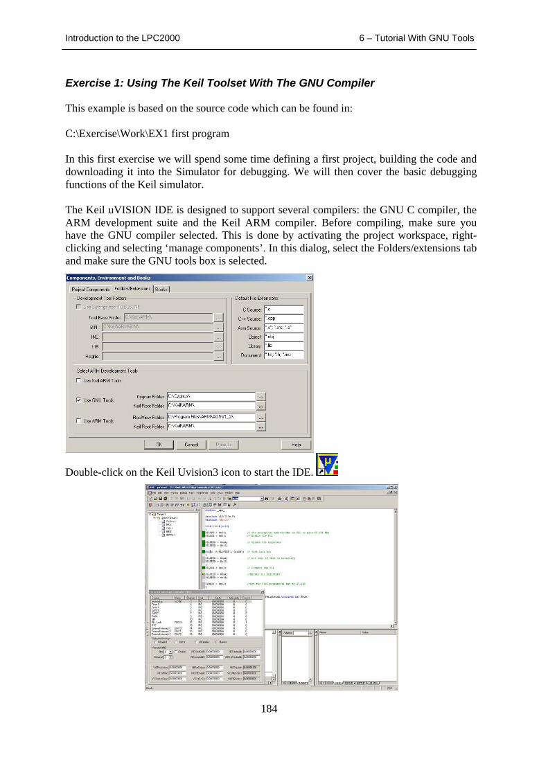
Introduction to the LPC2000 6 – Tutorial With GNU Tools
184
Exercise 1: Using The Keil Toolset With The GNU Compiler This example is based on the source code which can be found in: C:\Exercise\Work\EX1 first program In this first exercise we will spend some time defining a first project, building the code and downloading it into the Simulator for debugging. We will then cover the basic debugging functions of the Keil simulator. The Keil uVISION IDE is designed to support several compilers: the GNU C compiler, the ARM development suite and the Keil ARM compiler. Before compiling, make sure you have the GNU compiler selected. This is done by activating the project workspace, right-clicking and selecting ‘manage components’. In this dialog, select the Folders/extensions tab and make sure the GNU tools box is selected.
Double-click on the Keil Uvision3 icon to start the IDE.
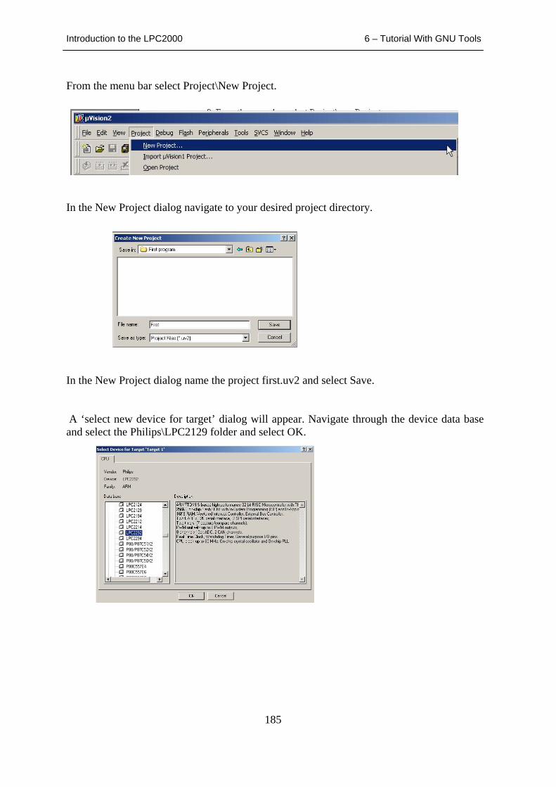
Introduction to the LPC2000 6 – Tutorial With GNU Tools
185
From the menu bar select Project\New Project.
In the New Project dialog navigate to your desired project directory.
In the New Project dialog name the project first.uv2 and select Save. A ‘select new device for target’ dialog will appear. Navigate through the device data base and select the Philips\LPC2129 folder and select OK.
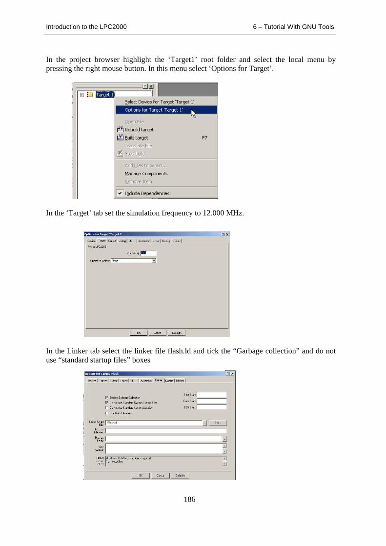
Introduction to the LPC2000 6 – Tutorial With GNU Tools
186
In the project browser highlight the ‘Target1’ root folder and select the local menu by pressing the right mouse button. In this menu select ‘Options for Target’.
In the ‘Target’ tab set the simulation frequency to 12.000 MHz.
In the Linker tab select the linker file flash.ld and tick the “Garbage collection” and do not use “standard startup files” boxes
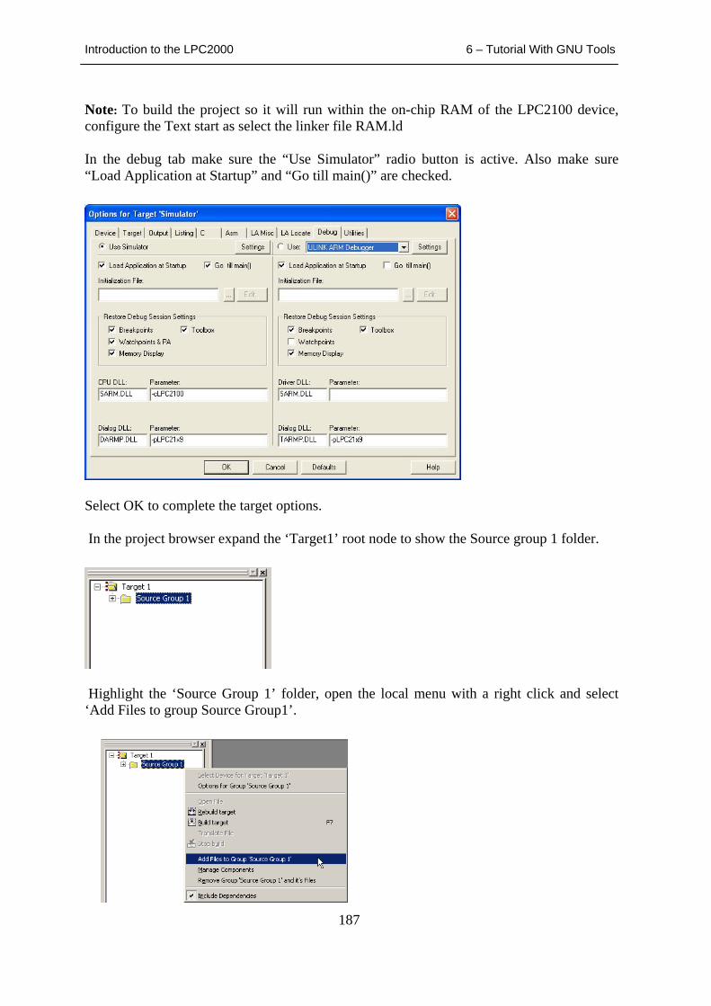
Introduction to the LPC2000 6 – Tutorial With GNU Tools
187
Note: To build the project so it will run within the on-chip RAM of the LPC2100 device, configure the Text start as select the linker file RAM.ld In the debug tab make sure the “Use Simulator” radio button is active. Also make sure “Load Application at Startup” and “Go till main()” are checked.
Select OK to complete the target options. In the project browser expand the ‘Target1’ root node to show the Source group 1 folder.
Highlight the ‘Source Group 1’ folder, open the local menu with a right click and select ‘Add Files to group Source Group1’.
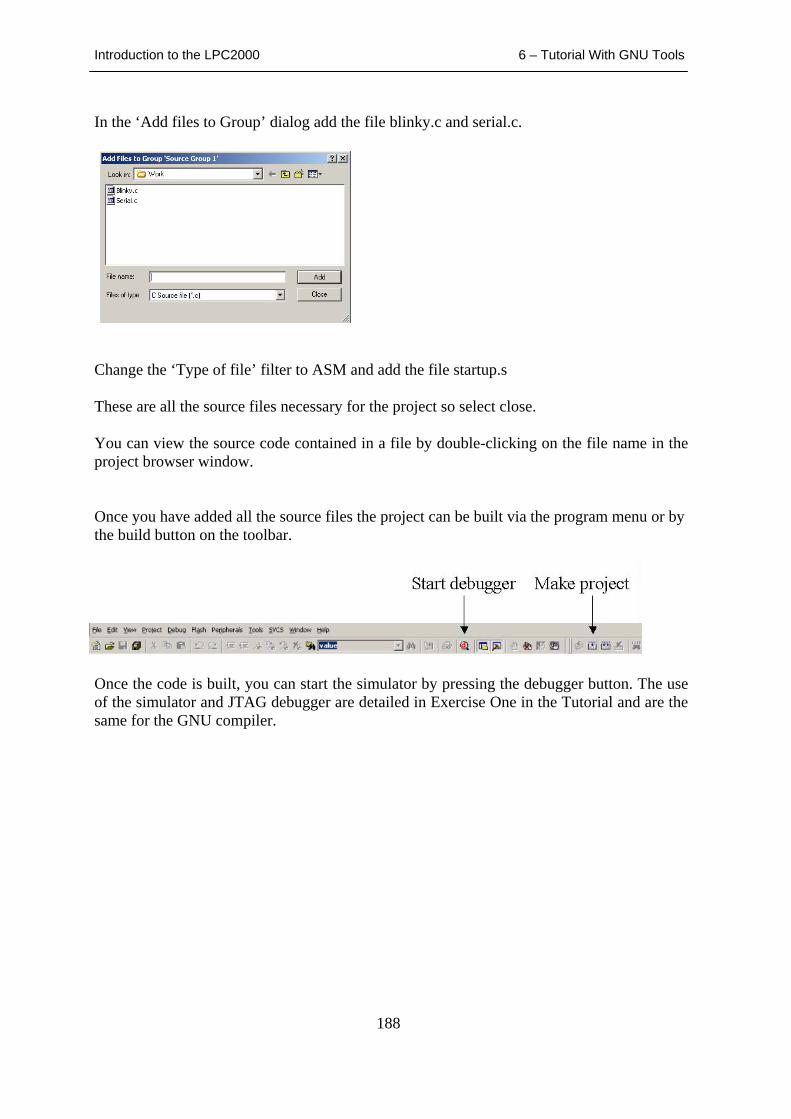
Introduction to the LPC2000 6 – Tutorial With GNU Tools
188
In the ‘Add files to Group’ dialog add the file blinky.c and serial.c.
Change the ‘Type of file’ filter to ASM and add the file startup.s These are all the source files necessary for the project so select close. You can view the source code contained in a file by double-clicking on the file name in the project browser window. Once you have added all the source files the project can be built via the program menu or by the build button on the toolbar.
Once the code is built, you can start the simulator by pressing the debugger button. The use of the simulator and JTAG debugger are detailed in Exercise One in the Tutorial and are the same for the GNU compiler.
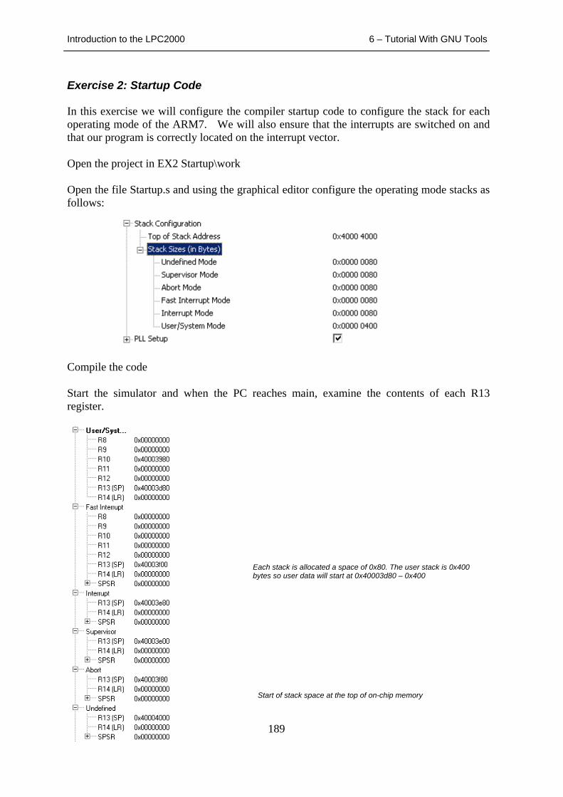
Introduction to the LPC2000 6 – Tutorial With GNU Tools
189
Exercise 2: Startup Code In this exercise we will configure the compiler startup code to configure the stack for each operating mode of the ARM7. We will also ensure that the interrupts are switched on and that our program is correctly located on the interrupt vector. Open the project in EX2 Startup\work Open the file Startup.s and using the graphical editor configure the operating mode stacks as follows:
Compile the code Start the simulator and when the PC reaches main, examine the contents of each R13 register.
Start of stack space at the top of on-chip memory
Each stack is allocated a space of 0x80. The user stack is 0x400 bytes so user data will start at 0x40003d80 – 0x400
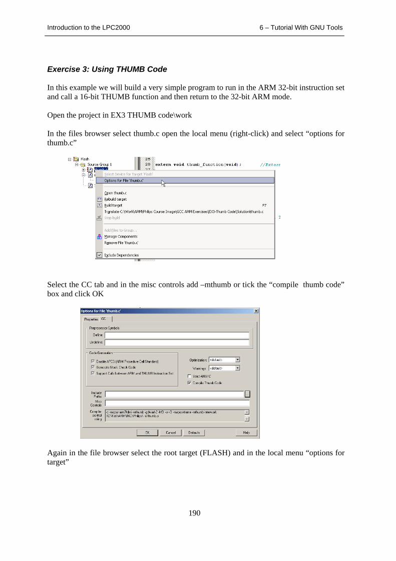
Introduction to the LPC2000 6 – Tutorial With GNU Tools
190
Exercise 3: Using THUMB Code In this example we will build a very simple program to run in the ARM 32-bit instruction set and call a 16-bit THUMB function and then return to the 32-bit ARM mode. Open the project in EX3 THUMB code\work In the files browser select thumb.c open the local menu (right-click) and select “options for thumb.c”
Select the CC tab and in the misc controls add –mthumb or tick the “compile thumb code” box and click OK
Again in the file browser select the root target (FLASH) and in the local menu “options for target”
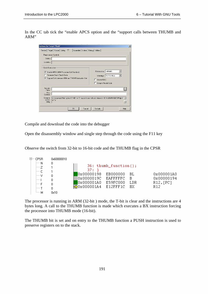
Introduction to the LPC2000 6 – Tutorial With GNU Tools
191
In the CC tab tick the “enable APCS option and the “support calls between THUMB and ARM”
Compile and download the code into the debugger Open the disassembly window and single step through the code using the F11 key Observe the switch from 32-bit to 16-bit code and the THUMB flag in the CPSR
The processor is running in ARM (32-bit ) mode, the T-bit is clear and the instructions are 4 bytes long. A call to the THUMB function is made which executes a BX instruction forcing the processor into THUMB mode (16-bit). The THUMB bit is set and on entry to the THUMB function a PUSH instruction is used to preserve registers on to the stack.
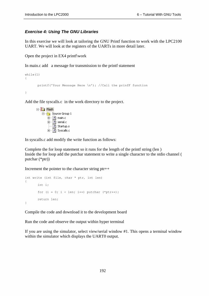
Introduction to the LPC2000 6 – Tutorial With GNU Tools
192
Exercise 4: Using The GNU Libraries In this exercise we will look at tailoring the GNU Printf function to work with the LPC2100 UART. We will look at the registers of the UARTs in more detail later. Open the project in EX4 printf\work In main.c add a message for transmission to the printf statement while(1) {
printf("Your Message Here \n"); //Call the prinfF function }
Add the file syscalls.c in the work directory to the project.
In syscalls.c add modify the write function as follows: Complete the for loop statement so it runs for the length of the printf string (len ) Inside the for loop add the putchar statement to write a single character to the stdio channel ( putchar (*ptr)) Increment the pointer to the character string ptr++ int write (int file, char * ptr, int len) { int i; for (i = 0; i < len; i++) putchar (*ptr++);
return len; }
Compile the code and download it to the development board Run the code and observe the output within hyper terminal If you are using the simulator, select view/serial window #1. This opens a terminal window within the simulator which displays the UART0 output.
Introduction to the LPC2000 6 – Tutorial With GNU Tools
193
Exercise 5: Simple Interrupt 1. In this exercise we will setup a basic FIQ interrupt and see it serviced. 2. Open the project in EX5-Interrupt\work 3. In main.c complete the definition of the EXTintFIQ function prototype to define it as the FIQ interrupt service routine void EXTintFIQ (void) __attribute__ ((interrupt("FIQ")));
In startup.s complete the vector constants table to define EXTintFIQ as the FIQ ISR. .global EXTintFIQ Declare the name of the C ISR function as a global .global _startup .func _startup _startup: Vectors: LDR PC, Reset_Addr LDR PC, Undef_Addr LDR PC, SWI_Addr LDR PC, PAbt_Addr Vector Table LDR PC, DAbt_Addr .long 0xB8A06F58 LDR PC, [PC, #-0xFF0] LDR PC, FIQ_Addr Reset_Addr: .word Reset_Handler Undef_Addr: .word Undef_Handler SWI_Addr: .word SWI_Handler Constants table PAbt_Addr: .word PAbt_Handler DAbt_Addr: .word DAbt_Handler .word 0 IRQ_Addr: .word IRQ_Handler FIQ_Addr: .word EXTintFIQ
Insert the name of the C ISR function in the constants table 5. Compile the code and download it onto the board. 6. Step through the code and observe the following using the disassembly window and the registers window. Step through the code until you reach the while loop c. Set a breakpoint in the EXTintFIQ function Press F5 to set the program running On the MCB2100 board press the INT button to generate the interrupt. If you want to see the entry and exit mechanisms to the exception, it is best to use the simulator and single step in the disassembly window. This way you can watch the program flow and the actions on the CPU registers.
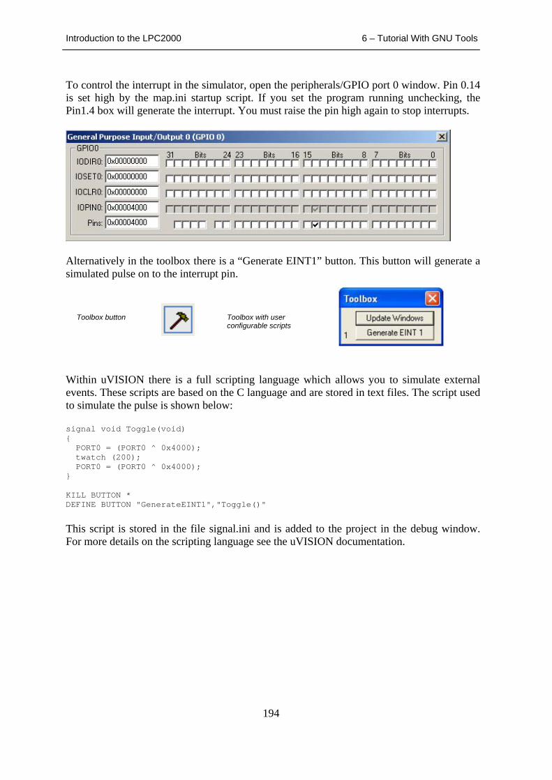
Introduction to the LPC2000 6 – Tutorial With GNU Tools
194
To control the interrupt in the simulator, open the peripherals/GPIO port 0 window. Pin 0.14 is set high by the map.ini startup script. If you set the program running unchecking, the Pin1.4 box will generate the interrupt. You must raise the pin high again to stop interrupts.
Alternatively in the toolbox there is a “Generate EINT1” button. This button will generate a simulated pulse on to the interrupt pin.
Within uVISION there is a full scripting language which allows you to simulate external events. These scripts are based on the C language and are stored in text files. The script used to simulate the pulse is shown below: signal void Toggle(void) { PORT0 = (PORT0 ^ 0x4000); twatch (200); PORT0 = (PORT0 ^ 0x4000); } KILL BUTTON * DEFINE BUTTON "GenerateEINT1","Toggle()"
This script is stored in the file signal.ini and is added to the project in the debug window. For more details on the scripting language see the uVISION documentation.
Toolbox button Toolbox with user configurable scripts
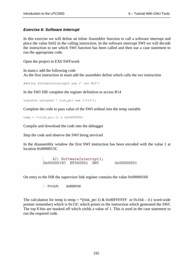
Introduction to the LPC2000 6 – Tutorial With GNU Tools
195
Exercise 6: Software Interrupt In this exercise we will define an inline Assembler function to call a software interrupt and place the value 0x02 in the calling instruction. In the software interrupt SWI we will decode the instruction to see which SWI function has been called and then use a case statement to run the appropriate code. Open the project in EX6 SWI\work In main.c add the following code As the first instruction in main add the assembler define which calls the swi instruction #define SoftwareInterrupt2 asm (" swi #02")
In the SWI ISR complete the register definition to access R14 register unsigned * link_ptr asm ("r14");
Complete the code to pass value of the SWI ordinal into the temp variable temp = *(link_ptr-1) & 0x00FFFFFF;
Compile and download the code into the debugger Step the code and observe the SWI being serviced In the disassembly window the first SWI instruction has been encoded with the value 1 at location 0x0000015C
On entry to the ISR the supervisor link register contains the value 0x00000160
The calculation for temp is temp = *(link_ptr-1) & 0x00FFFFFF or 0x164 – 4 ( word-wide pointer remember) which is 0x15C which points to the instruction which generated the SWI. The top 8 bits are masked off which yields a value of 1. This is used in the case statement to run the required code.

Introduction to the LPC2000 6 – Tutorial With GNU Tools
196

197
Appendices Appendix A Bibliography ARM7TDMI datasheet ARM LPC2119/2129/2194/2292/2294 User Manual Philips ARM System on chip architecture Steve Furber Architecture Reference Manual David Seal ARM System developers guide Andrew N. Sloss,
Domonic Symes, Chris Wright
MicroC/OS-II Jean J. Labrosse GCC The complete reference Arthur Griffith Webliography Reference Sites http://www.arm.com http://www.philips.com http://www.lpc2000.com Tools and Software Development http://ww.hitex.co.uk http://www.keil.co.uk http://www.ucos-ii.com http://www.ristancase.com http://gcc.gnu.org/onlinedocs/gcc/ Evaluation Boards And Modules http://www.phytec.co.uk http://www.embeddedartists.com

198

The LPC2000 family from Philips semiconductors is the first of a new generation of microcontrollers based on the ARM7-TDMI 16/32-bit RISC processor. This book is written as both an introduction to the ARM7-TDMI processor and the LPC2000 microcontroller architecture. The content is based on a series of one day seminars held for professional engineers interested in learning how to use the LPC2000 family as quickly as possible.
Topics covered in this book include:
- Introduction to the ARM7 processor- Software development tools- LPC2000 system architecture- LPC2000 peripherals
In addition a comprehensive tutorial is included that takes you through practical exercises to reinforce the topics discussed in the main text. By reading this book and performing the accompanying exercises, you will quickly become well versed in the ARM7 processor and the LPC2000 microcontroller.
The CD accompanying the book includes an evaluation version of the popular uVISION3 IDE and compiler from Keil Elektronik plus all the example exercises for both the Keil CARM and the GCC ARM compilers.
www.hitex.co.uk/arm
Hitex (UK) Ltd., Sir William Lyons Road, Science Park, Coventry, UK, CV4 7EZ. Tel +44 (0) 2476 692066
9 7 8 0 9 5 4 9 9 8 8 1 3
ISBN 0 - 9549988 - 1 - 2
Related Documents