1 G. Betti Beneventi Technology Computer Aided Design (TCAD) Laboratory Lecture 4, the ideal diode (pn-junction) Giovanni Betti Beneventi E-mail: [email protected] ; [email protected] Office: Engineering faculty, ARCES lab. (Ex. 3.2 room), viale del Risorgimento 2, Bologna Phone: +39-051-209-3773 Advanced Research Center on Electronic Systems (ARCES) University of Bologna, Italy [Source: Synopsys]

Welcome message from author
This document is posted to help you gain knowledge. Please leave a comment to let me know what you think about it! Share it to your friends and learn new things together.
Transcript
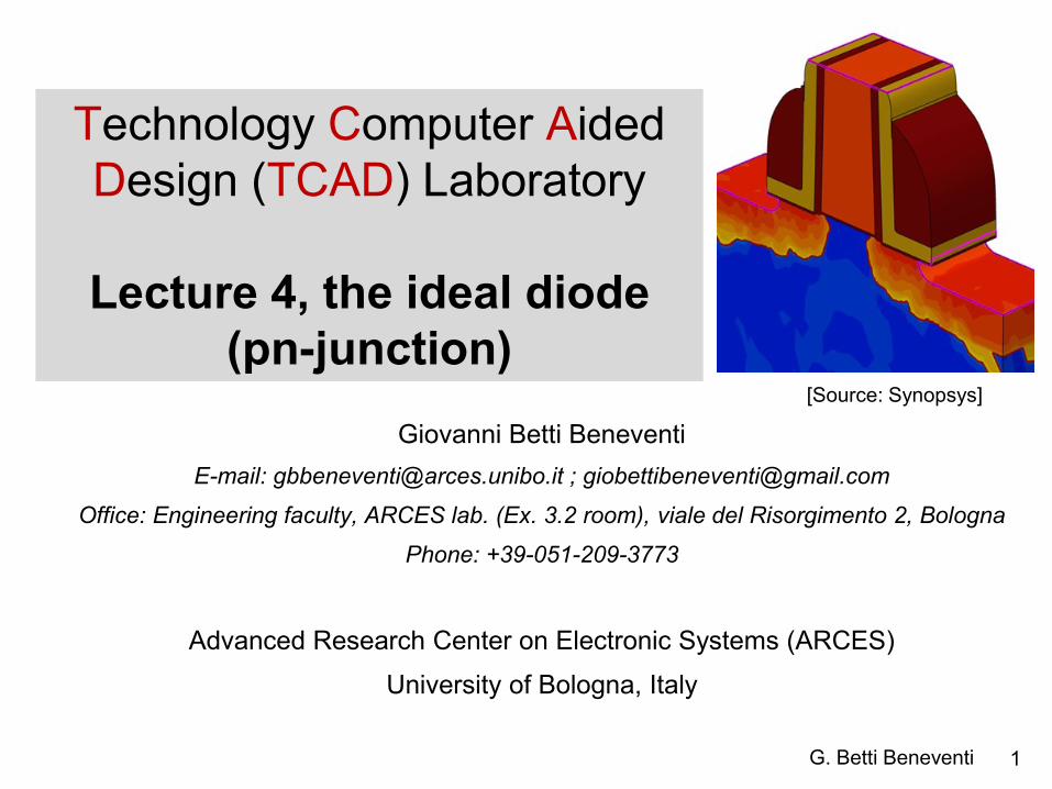
1 G. Betti Beneventi
Technology Computer Aided
Design (TCAD) Laboratory
Lecture 4, the ideal diode
(pn-junction)
Giovanni Betti Beneventi
E-mail: [email protected] ; [email protected]
Office: Engineering faculty, ARCES lab. (Ex. 3.2 room), viale del Risorgimento 2, Bologna
Phone: +39-051-209-3773
Advanced Research Center on Electronic Systems (ARCES)
University of Bologna, Italy
[Source: Synopsys]
2 G. Betti Beneventi
Outline
• Review of basic properties of the diode
• Sentaurus Workbench setup (SWB)
• Implementation of Input files
– Sentaurus Structure Editor (SDE) command file
– Sentaurus Device (SDevice)
• command file
• parameter file
• Run the simulation
• Post-processing of results
3 G. Betti Beneventi
Outline
Review of basic properties of the diode
• Sentaurus Workbench setup (SWB)
• Implementation of Input files
– Sentaurus Structure Editor (SDE) command file
– Sentaurus Device (SDevice)
• command file
• parameter file
• Run the simulation
• Post-processing of results
4 G. Betti Beneventi
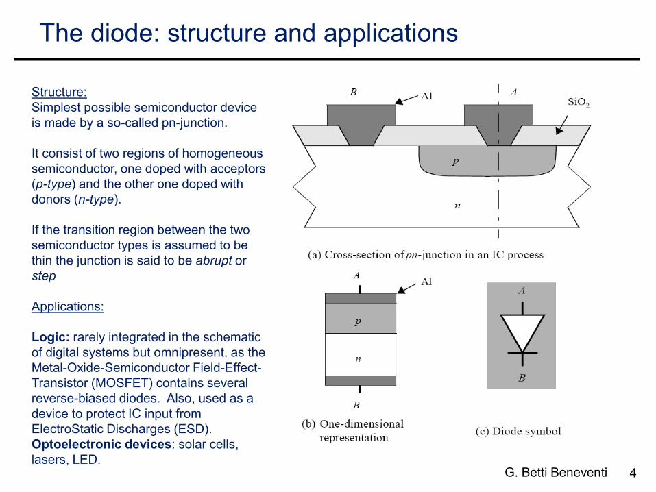
The diode: structure and applications
Structure:
Simplest possible semiconductor device
is made by a so-called pn-junction.
It consist of two regions of homogeneous
semiconductor, one doped with acceptors
(p-type) and the other one doped with
donors (n-type).
If the transition region between the two
semiconductor types is assumed to be
thin the junction is said to be abrupt or
step
Applications:
Logic: rarely integrated in the schematic
of digital systems but omnipresent, as the
Metal-Oxide-Semiconductor Field-Effect-
Transistor (MOSFET) contains several
reverse-biased diodes. Also, used as a
device to protect IC input from
ElectroStatic Discharges (ESD).
Optoelectronic devices: solar cells,
lasers, LED.
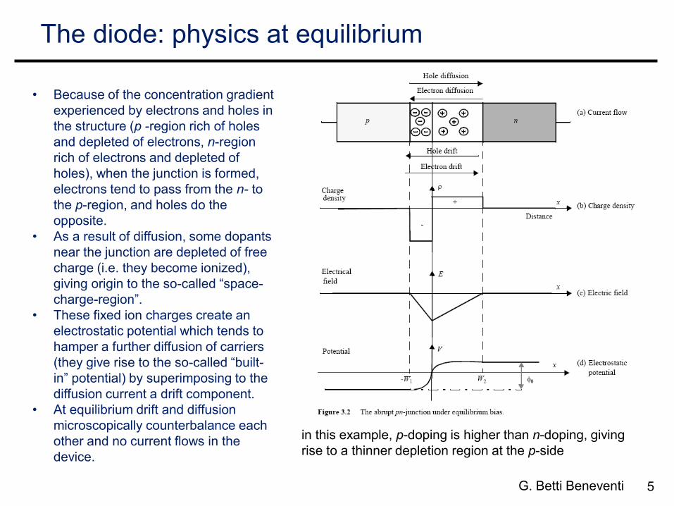
5 G. Betti Beneventi
The diode: physics at equilibrium
• Because of the concentration gradient
experienced by electrons and holes in
the structure (p -region rich of holes
and depleted of electrons, n-region
rich of electrons and depleted of
holes), when the junction is formed,
electrons tend to pass from the n- to
the p-region, and holes do the
opposite.
• As a result of diffusion, some dopants
near the junction are depleted of free
charge (i.e. they become ionized),
giving origin to the so-called “space-
charge-region”.
• These fixed ion charges create an
electrostatic potential which tends to
hamper a further diffusion of carriers
(they give rise to the so-called “built-
in” potential) by superimposing to the
diffusion current a drift component.
• At equilibrium drift and diffusion
microscopically counterbalance each
other and no current flows in the
device.
in this example, p-doping is higher than n-doping, giving
rise to a thinner depletion region at the p-side
6 G. Betti Beneventi
The diode: built-in potential
• If 𝑁𝐴 is the concentration of acceptors
at the p-side, and 𝑁𝐷 is the
concentration of donors art the n-side,
it can be shown that, if the
semiconductors are non-
degenerate, the built-in potential 𝜑0
is given by the formula (1), where the
thermal voltage 𝜑𝑇= 𝑘𝑇/𝑞= 26mV at
room temperature, and where 𝑛𝑖 is the
semiconductor intrinsic carrier
density, which is a material property
(depends on density of states and on
band-gap)
• Therefore, the higher the product of
the p and n doping, the higher 𝝋𝟎
• The built-in potential is “built-in” since
it is an intrinsic property of the
junction. It represents the energy
barrier that majority carriers (electron
in n-region, holes in p-region) have to
overcome in order to obtain a net
current flow by diffusion
𝜑0 = 𝜑𝑇 ln𝑁𝐴𝑁𝐷
𝑛𝑖2
Example (Silicon)
If 𝑁𝐴 = 1016𝑐𝑚−3, and 𝑁𝐷 = 1016𝑐𝑚−3 , 𝑛𝑖 ≅ 1.5𝑥1010 𝑐𝑚−3, 𝜑0 = 697 mV
(1)
• By modulating the built-in voltage using an external
battery it is possible to modulate the behavior of the
device. In particular:
• The application of a positive voltage at the p-region
(or, equivalently, a negative voltage at the n-region)
lowers the potential barriers, and current can flow by
diffusion through the space-charge region. In this
regime, current increases exponentially with voltage
and the diode is said to be forward biased.
• The application of a negative voltage at the p-region
(or, equivalently, a positive voltage at the n-region)
further increases the potential barrier, current can flow
only by drift of minority carriers, it is very weak and
almost independent by voltage. In this regime, the
diode is said to be reverse biased.
7 G. Betti Beneventi
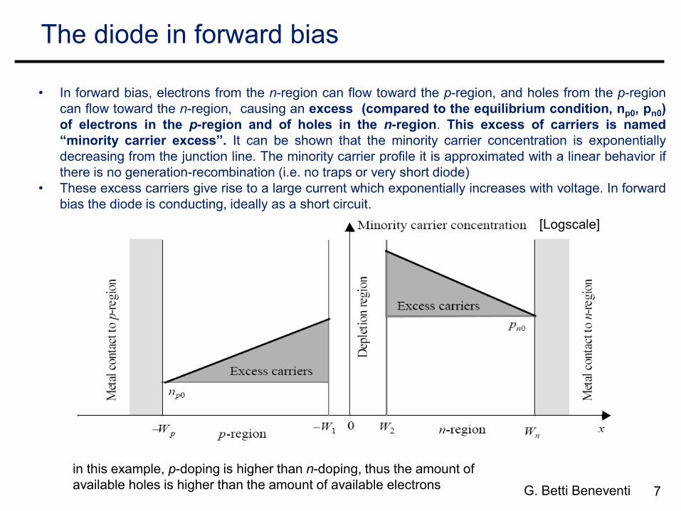
The diode in forward bias
• In forward bias, electrons from the n-region can flow toward the p-region, and holes from the p-region
can flow toward the n-region, causing an excess (compared to the equilibrium condition, np0, pn0)
of electrons in the p-region and of holes in the n-region. This excess of carriers is named
“minority carrier excess”. It can be shown that the minority carrier concentration is exponentially
decreasing from the junction line. The minority carrier profile it is approximated with a linear behavior if
there is no generation-recombination (i.e. no traps or very short diode)
• These excess carriers give rise to a large current which exponentially increases with voltage. In forward
bias the diode is conducting, ideally as a short circuit.
in this example, p-doping is higher than n-doping, thus the amount of
available holes is higher than the amount of available electrons
[Logscale]
8 G. Betti Beneventi
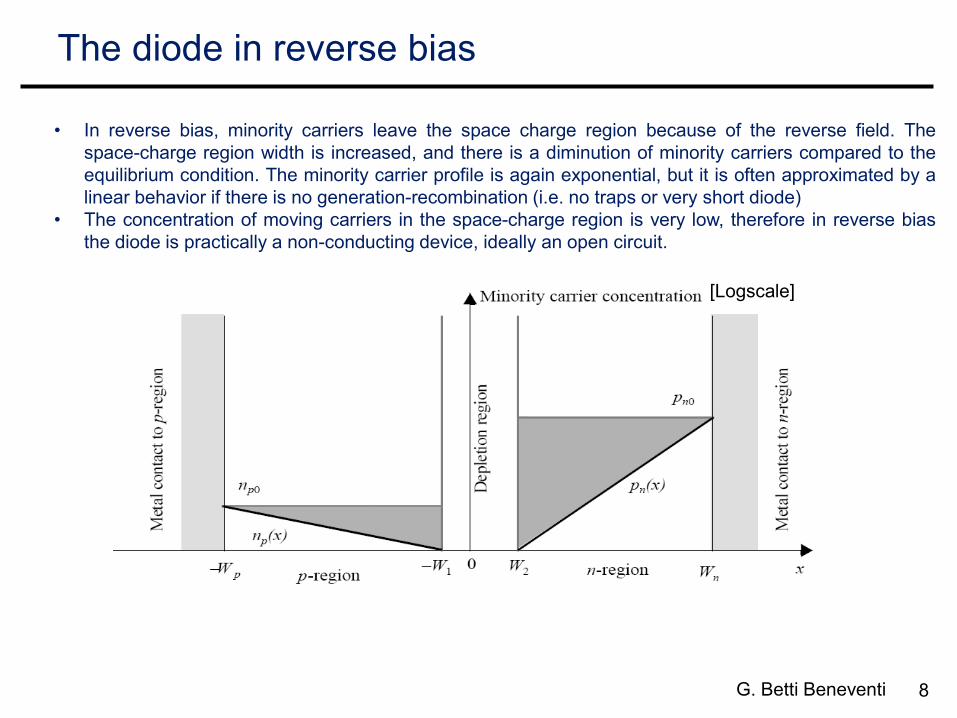
The diode in reverse bias
• In reverse bias, minority carriers leave the space charge region because of the reverse field. The
space-charge region width is increased, and there is a diminution of minority carriers compared to the
equilibrium condition. The minority carrier profile is again exponential, but it is often approximated by a
linear behavior if there is no generation-recombination (i.e. no traps or very short diode)
• The concentration of moving carriers in the space-charge region is very low, therefore in reverse bias
the diode is practically a non-conducting device, ideally an open circuit.
[Logscale]
9 G. Betti Beneventi
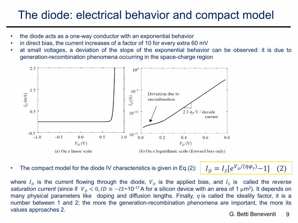
• the diode acts as a one-way conductor with an exponential behavior
• in direct bias, the current increases of a factor of 10 for every extra 60 mV
• at small voltages, a deviation of the slope of the exponential behavior can be observed: it is due to
generation-recombination phenomena occurring in the space-charge region
• The compact model for the diode IV characteristics is given in Eq.(2):
where 𝐼𝐷 is the current flowing through the diode, 𝑉𝐷 is the applied bias, and 𝐼𝑆 is called the reverse
saturation current (since if 𝑉𝐷 < 0, 𝐼𝐷 ≅ −𝐼𝑆~10-17 A for a silicon device with an area of 1 mm2). It depends on
many physical parameters like doping and diffusion lengths. Finally, 𝜂 is called the ideality factor, it is a
number between 1 and 2; the more the generation-recombination phenomena are important, the more its
values approaches 2.
The diode: electrical behavior and compact model
𝐼𝐷 = 𝐼𝑆[𝑒𝑉𝐷
/(𝜂𝜑𝑇)−1] (2)
10 G. Betti Beneventi
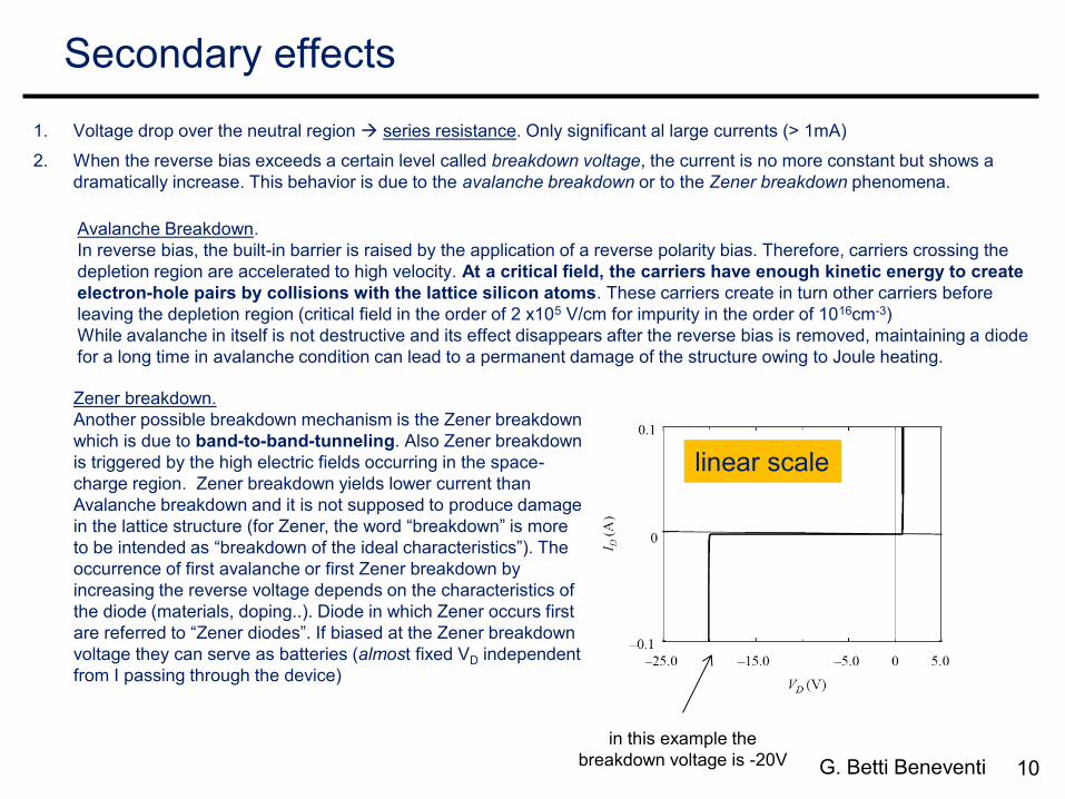
Secondary effects
1. Voltage drop over the neutral region series resistance. Only significant al large currents (> 1mA)
2. When the reverse bias exceeds a certain level called breakdown voltage, the current is no more constant but shows a
dramatically increase. This behavior is due to the avalanche breakdown or to the Zener breakdown phenomena.
Avalanche Breakdown.
In reverse bias, the built-in barrier is raised by the application of a reverse polarity bias. Therefore, carriers crossing the
depletion region are accelerated to high velocity. At a critical field, the carriers have enough kinetic energy to create
electron-hole pairs by collisions with the lattice silicon atoms. These carriers create in turn other carriers before
leaving the depletion region (critical field in the order of 2 x10⁵ V/cm for impurity in the order of 1016cm-3)
While avalanche in itself is not destructive and its effect disappears after the reverse bias is removed, maintaining a diode
for a long time in avalanche condition can lead to a permanent damage of the structure owing to Joule heating.
Zener breakdown.
Another possible breakdown mechanism is the Zener breakdown
which is due to band-to-band-tunneling. Also Zener breakdown
is triggered by the high electric fields occurring in the space-
charge region. Zener breakdown yields lower current than
Avalanche breakdown and it is not supposed to produce damage
in the lattice structure (for Zener, the word “breakdown” is more
to be intended as “breakdown of the ideal characteristics”). The
occurrence of first avalanche or first Zener breakdown by
increasing the reverse voltage depends on the characteristics of
the diode (materials, doping..). Diode in which Zener occurs first
are referred to “Zener diodes”. If biased at the Zener breakdown
voltage they can serve as batteries (almost fixed VD independent
from I passing through the device)
in this example the
breakdown voltage is -20V
linear scale
11 G. Betti Beneventi
Outline
• Review of basic properties of the diode
Sentaurus Workbench setup (SWB)
• Implementation of Input files
– Sentaurus Structure Editor (SDE) command file
– Sentaurus Device (SDevice)
• command file
• parameter file
• Run the simulation
• Post-processing of results
12 G. Betti Beneventi
SWB: project tools & parameters (1)
OPEN SWB FROM THE LINUX COMMAND LINE swb &
STARTING (AND SAVING) A NEW SWB PROJECT Project New New Project
Project Save as Project pn_ideale
ADD TOOLS left click on No tools right click Add Name, scroll for Sde select Batch Ok
left click on Sde right click Add Name scroll for Sdevice Ok
BATCH MODE MEANS “COMMAND FILE MODE”, i.e. NOT INTERACTIVE
ADD PARAMETERS (WITH THEIR DEFAULT VALUES): SDE /GEOMETRY AND DOPING Right click in the box just below SDE tool SRH default value 0
Parameter Add Parameter material default value Silicon Ok
Right click on material Add Parameter Wp default value 10
IN SENTAURUS, THE GEOMETRICAL DIMENSIONS ARE INTENDED IN MICRON (=1x10⁻⁶ m) Right click on Wp Add Parameter Wn default value 50
Right click on Wn Add Parameter p_doping default value 1e16
IN SENTAURUS, DOPING IS INTENDED IN cm-3 Right click on p_doping Add Parameter n_doping1e16
ADD PARAMETERS (WITH THEIR DEFAULT VALUES): SDEVICE /MODELS AND VOLTAGES Right click in the box just below Sdevice tool SRH default value 0
FLAG FOR ACTIVATING SHOCKLEY-READ-HALL GENERATION-RECOMBINATION MODEL
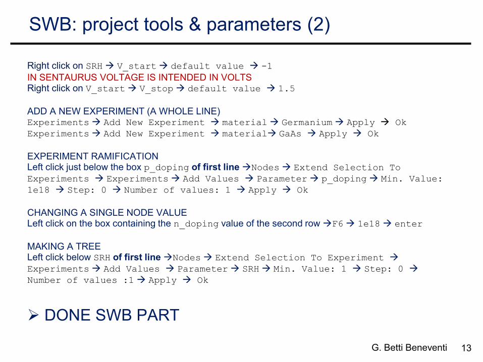
13 G. Betti Beneventi
SWB: project tools & parameters (2)
Right click on SRH V_start default value -1
IN SENTAURUS VOLTAGE IS INTENDED IN VOLTS Right click on V_start V_stop default value 1.5
ADD A NEW EXPERIMENT (A WHOLE LINE) Experiments Add New Experiment material Germanium Apply Ok
Experiments Add New Experiment material GaAs Apply Ok
EXPERIMENT RAMIFICATION Left click just below the box p_doping of first line Nodes Extend Selection To
Experiments Experiments Add Values Parameter p_doping Min. Value:
1e18 Step: 0 Number of values: 1 Apply Ok
CHANGING A SINGLE NODE VALUE Left click on the box containing the n_doping value of the second row F6 1e18 enter
MAKING A TREE Left click below SRH of first line Nodes Extend Selection To Experiment
Experiments Add Values Parameter SRH Min. Value: 1 Step: 0
Number of values :1 Apply Ok
DONE SWB PART
14 G. Betti Beneventi
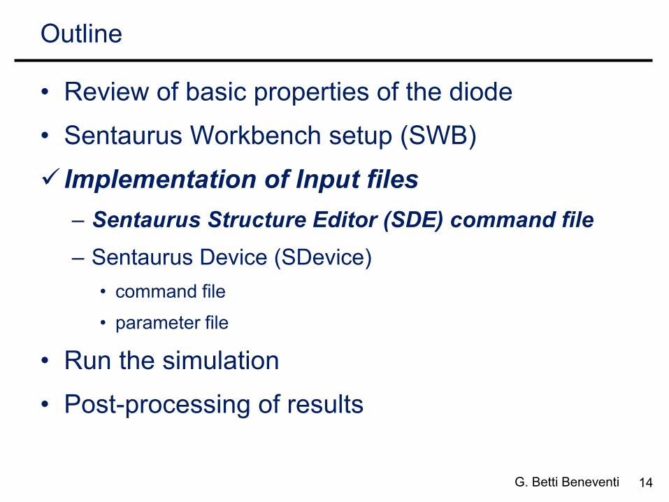
Outline
• Review of basic properties of the diode
• Sentaurus Workbench setup (SWB)
Implementation of Input files
– Sentaurus Structure Editor (SDE) command file
– Sentaurus Device (SDevice)
• command file
• parameter file
• Run the simulation
• Post-processing of results
15 G. Betti Beneventi
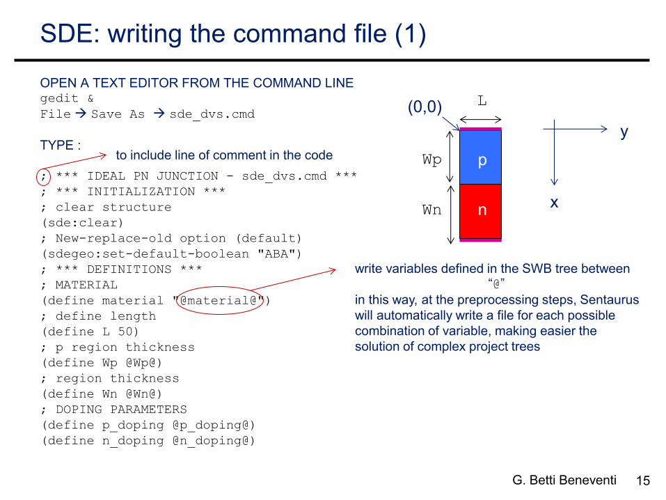
SDE: writing the command file (1)
OPEN A TEXT EDITOR FROM THE COMMAND LINE gedit &
File Save As sde_dvs.cmd
TYPE :
; *** IDEAL PN JUNCTION - sde_dvs.cmd ***
; *** INITIALIZATION ***
; clear structure
(sde:clear)
; New-replace-old option (default)
(sdegeo:set-default-boolean "ABA")
; *** DEFINITIONS ***
; MATERIAL
(define material "@material@")
; define length
(define L 50)
; p region thickness
(define Wp @Wp@)
; region thickness
(define Wn @Wn@)
; DOPING PARAMETERS
(define p_doping @p_doping@)
(define n_doping @n_doping@)
to include line of comment in the code
write variables defined in the SWB tree between “@”
in this way, at the preprocessing steps, Sentaurus
will automatically write a file for each possible
combination of variable, making easier the
solution of complex project trees
L
Wp
Wn
p
n
y
x
(0,0)
16 G. Betti Beneventi
SDE command file (2)
; MESH PARAMETERS
(define xmax 10)
(define xmin 0.1)
(define ymax 1)
(define ymin 0.1) ; *** GEOMETRY ***
; convention: x=length y=thickness
; create p region
(sdegeo:create-rectangle (position 0 0 0) (position L Wp 0) material "p-region")
; create n region
(sdegeo:create-rectangle (position 0 Wp 0) (position L (+ Wn Wp) 0) material "n-
region")
; *** CONTACTS ***
; a) SET VERTEXES
; 1st vertex on p_contact
(sdegeo:insert-vertex (position 0 0 0))
; 2nd vertex on p_contact
(sdegeo:insert-vertex (position L 0 0))
; 1st vertex on n_contact
(sdegeo:insert-vertex (position 0 (+ Wn Wp) 0))
; 2nd vertex on n_contact
(sdegeo:insert-vertex (position L (+ Wn Wp) 0))
17 G. Betti Beneventi
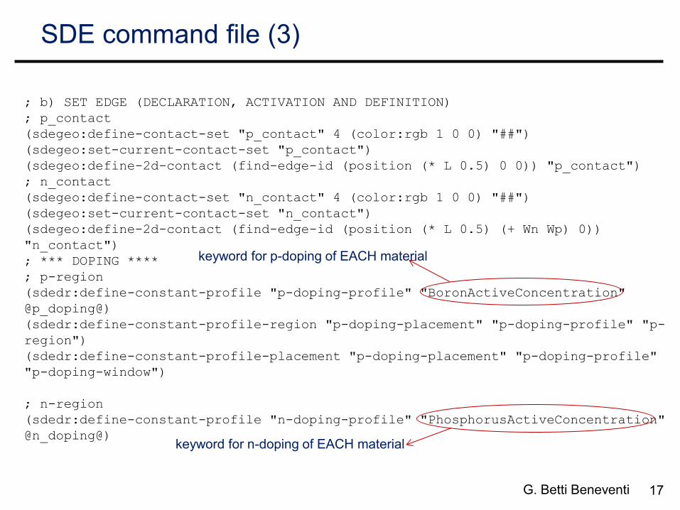
SDE command file (3)
; b) SET EDGE (DECLARATION, ACTIVATION AND DEFINITION)
; p_contact
(sdegeo:define-contact-set "p_contact" 4 (color:rgb 1 0 0) "##")
(sdegeo:set-current-contact-set "p_contact")
(sdegeo:define-2d-contact (find-edge-id (position (* L 0.5) 0 0)) "p_contact")
; n_contact
(sdegeo:define-contact-set "n_contact" 4 (color:rgb 1 0 0) "##")
(sdegeo:set-current-contact-set "n_contact")
(sdegeo:define-2d-contact (find-edge-id (position (* L 0.5) (+ Wn Wp) 0))
"n_contact")
; *** DOPING ****
; p-region
(sdedr:define-constant-profile "p-doping-profile" "BoronActiveConcentration"
@p_doping@)
(sdedr:define-constant-profile-region "p-doping-placement" "p-doping-profile" "p-
region")
(sdedr:define-constant-profile-placement "p-doping-placement" "p-doping-profile"
"p-doping-window")
; n-region
(sdedr:define-constant-profile "n-doping-profile" "PhosphorusActiveConcentration"
@n_doping@)
keyword for p-doping of EACH material
keyword for n-doping of EACH material
18 G. Betti Beneventi
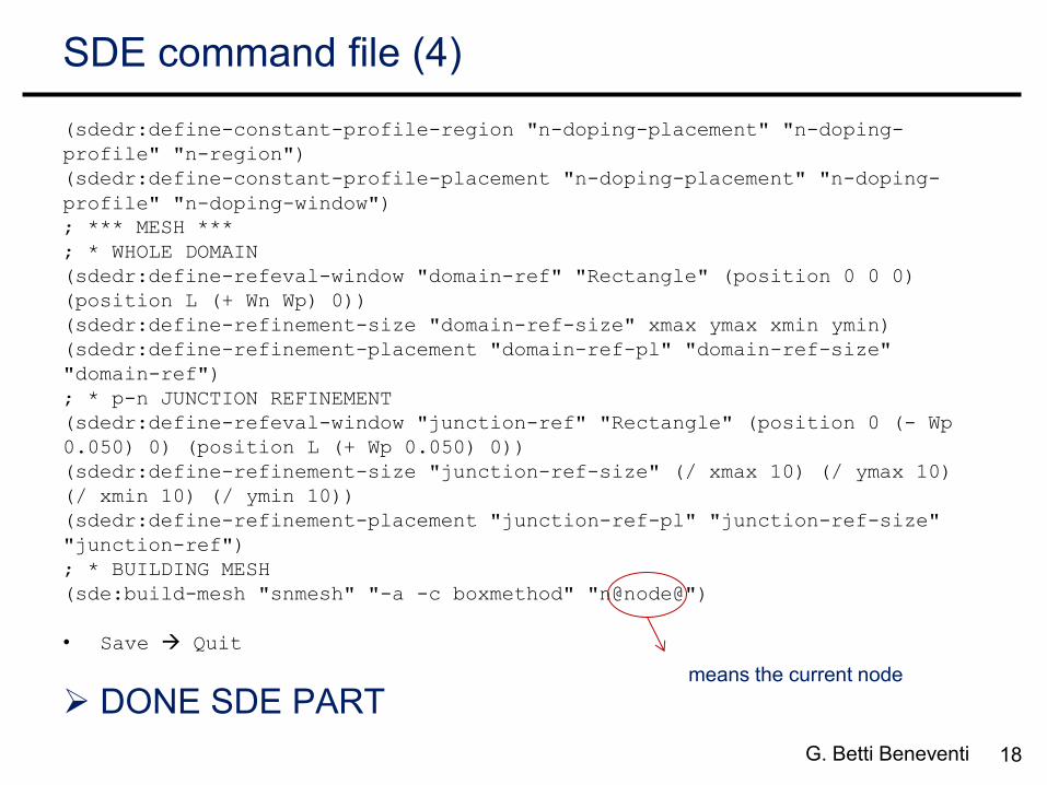
SDE command file (4)
(sdedr:define-constant-profile-region "n-doping-placement" "n-doping-
profile" "n-region")
(sdedr:define-constant-profile-placement "n-doping-placement" "n-doping-
profile" "n-doping-window") ; *** MESH ***
; * WHOLE DOMAIN
(sdedr:define-refeval-window "domain-ref" "Rectangle" (position 0 0 0)
(position L (+ Wn Wp) 0))
(sdedr:define-refinement-size "domain-ref-size" xmax ymax xmin ymin)
(sdedr:define-refinement-placement "domain-ref-pl" "domain-ref-size"
"domain-ref")
; * p-n JUNCTION REFINEMENT
(sdedr:define-refeval-window "junction-ref" "Rectangle" (position 0 (- Wp
0.050) 0) (position L (+ Wp 0.050) 0))
(sdedr:define-refinement-size "junction-ref-size" (/ xmax 10) (/ ymax 10)
(/ xmin 10) (/ ymin 10))
(sdedr:define-refinement-placement "junction-ref-pl" "junction-ref-size"
"junction-ref")
; * BUILDING MESH
(sde:build-mesh "snmesh" "-a -c boxmethod" "n@node@")
• Save Quit
DONE SDE PART
means the current node
19 G. Betti Beneventi
Outline
• Review of basic properties of the diode
• Sentaurus Workbench setup (SWB)
Implementation of Input files
– Sentaurus Structure Editor (SDE) command file
– Sentaurus Device (SDevice)
• command file
• parameter file
• Run the simulation
• Post-processing of results
20 G. Betti Beneventi
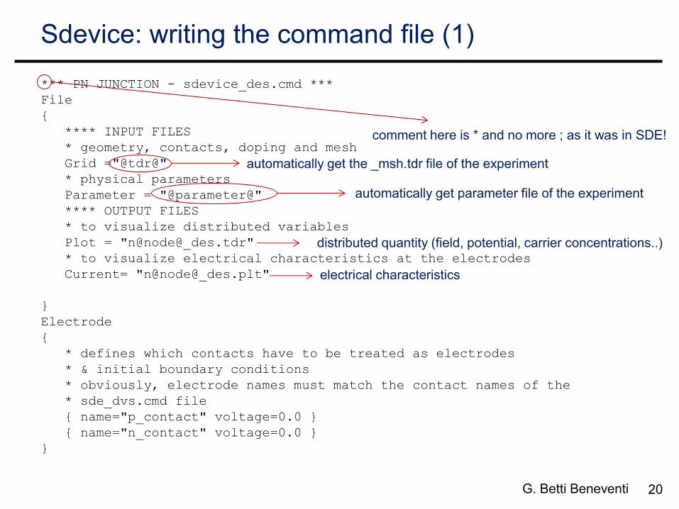
Sdevice: writing the command file (1)
*** PN JUNCTION - sdevice_des.cmd ***
File
{
**** INPUT FILES
* geometry, contacts, doping and mesh
Grid ="@tdr@"
* physical parameters
Parameter = "@parameter@"
**** OUTPUT FILES
* to visualize distributed variables
Plot = "n@node@_des.tdr"
* to visualize electrical characteristics at the electrodes
Current= "n@node@_des.plt"
}
Electrode
{
* defines which contacts have to be treated as electrodes
* & initial boundary conditions
* obviously, electrode names must match the contact names of the
* sde_dvs.cmd file
{ name="p_contact" voltage=0.0 }
{ name="n_contact" voltage=0.0 }
}
comment here is * and no more ; as it was in SDE!
automatically get the _msh.tdr file of the experiment
automatically get parameter file of the experiment
distributed quantity (field, potential, carrier concentrations..)
electrical characteristics
21 G. Betti Beneventi
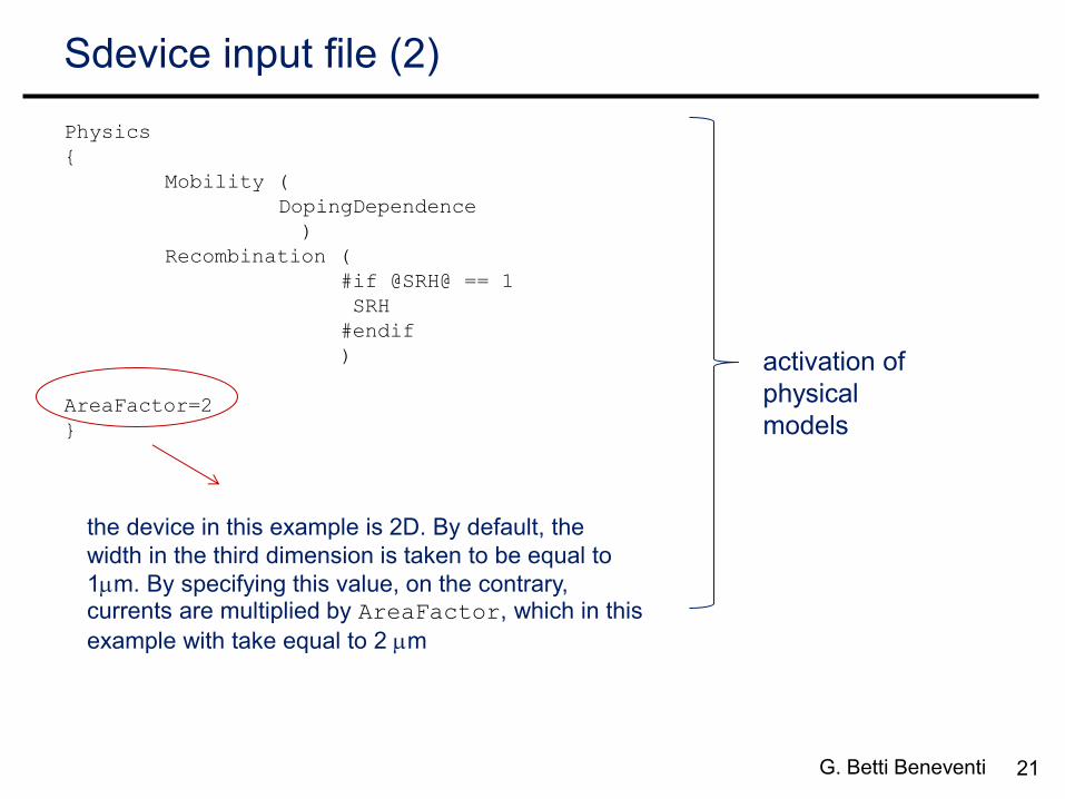
Sdevice input file (2)
Physics
{
Mobility (
DopingDependence
)
Recombination (
#if @SRH@ == 1
SRH
#endif
)
AreaFactor=2
}
activation of
physical
models
the device in this example is 2D. By default, the
width in the third dimension is taken to be equal to
1mm. By specifying this value, on the contrary, currents are multiplied by AreaFactor, which in this
example with take equal to 2 mm
22 G. Betti Beneventi
Sdevice command file (3)
Plot
{
* On-mesh-defined variables to be saved in the .tdr output file
*- Doping Profiles
Doping DonorConcentration AcceptorConcentration
*- Charge, field, potential and potential energy
SpaceCharge
ElectricField/Vector Potential
BandGap EffectiveBandGap BandGapNarrowing ElectronAffinity
ConductionBandEnergy ValenceBandEnergy
*- Carrier Densities:
EffectiveIntrinsicDensity IntrinsicDensity
eDensity hDensity
eQuasiFermiEnergy hQuasiFermiEnergy
*- Currents and current components:
eGradQuasiFermi/Vector hGradQuasiFermi/Vector
eMobility hMobility eVelocity hVelocity
Current/Vector eCurrent/Vector hCurrent/Vector
eDriftVelocity/Vector hDriftVelocity/Vector
*- SRH & interfacial traps
SRHrecombination
tSRHrecombination
These keywords under the Plot
section allow plotting the distributed
quantities simulated (both scalar
and vectors).
Some of the keywords refer to
quantities that are calculated only if
the respective physical model are
activated. Anyway, the keywords
can be included in the Plot section
command file even if the respective
models have not been activated
(useful to have a standard template
of Plot section)
23 G. Betti Beneventi
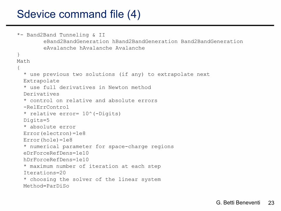
Sdevice command file (4)
*- Band2Band Tunneling & II
eBand2BandGeneration hBand2BandGeneration Band2BandGeneration
eAvalanche hAvalanche Avalanche
}
Math
{
* use previous two solutions (if any) to extrapolate next
Extrapolate
* use full derivatives in Newton method
Derivatives
* control on relative and absolute errors
-RelErrControl
* relative error= 10^(-Digits)
Digits=5
* absolute error
Error(electron)=1e8
Error(hole)=1e8
* numerical parameter for space-charge regions
eDrForceRefDens=1e10
hDrForceRefDens=1e10
* maximum number of iteration at each step
Iterations=20
* choosing the solver of the linear system
Method=ParDiSo
24 G. Betti Beneventi
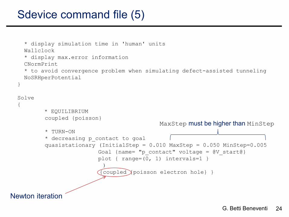
Sdevice command file (5)
* display simulation time in 'human' units
Wallclock
* display max.error information
CNormPrint
* to avoid convergence problem when simulating defect-assisted tunneling
NoSRHperPotential
}
Solve
{
* EQUILIBRIUM
coupled {poisson}
* TURN-ON
* decreasing p_contact to goal
quasistationary (InitialStep = 0.010 MaxStep = 0.050 MinStep=0.005
Goal {name= "p_contact" voltage = @V_start@}
plot { range=(0, 1) intervals=1 }
)
{coupled {poisson electron hole} }
Newton iteration
MaxStep must be higher than MinStep
25 G. Betti Beneventi
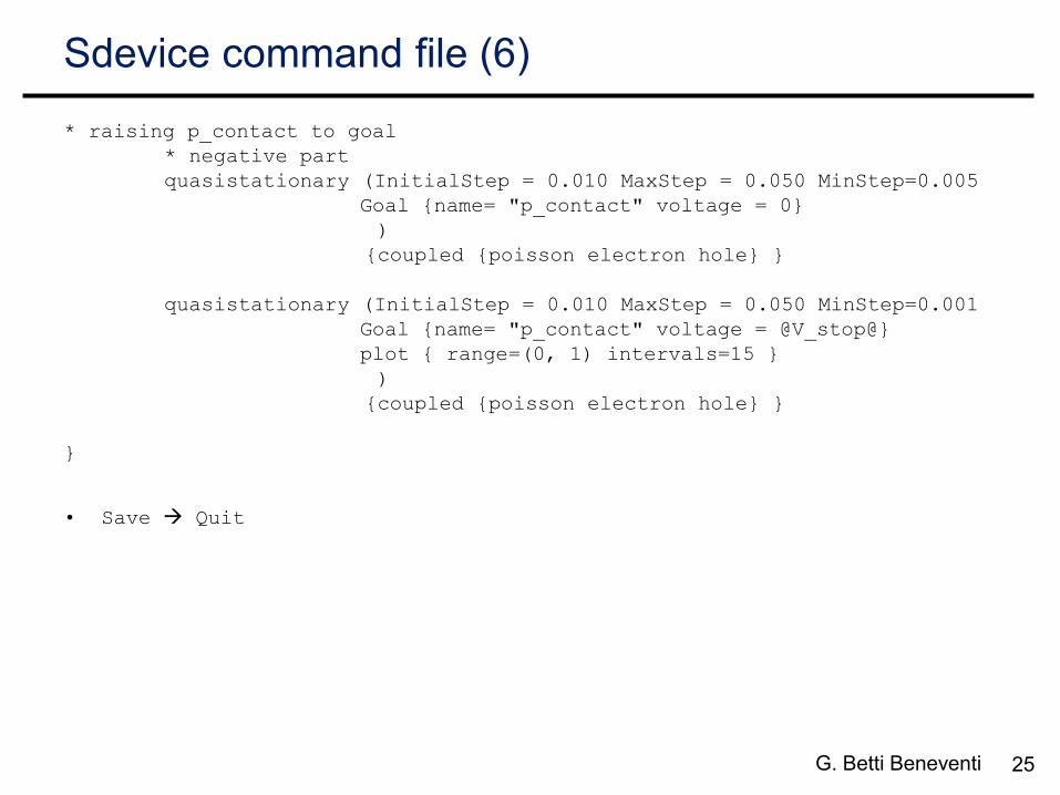
Sdevice command file (6)
* raising p_contact to goal
* negative part
quasistationary (InitialStep = 0.010 MaxStep = 0.050 MinStep=0.005
Goal {name= "p_contact" voltage = 0}
)
{coupled {poisson electron hole} }
quasistationary (InitialStep = 0.010 MaxStep = 0.050 MinStep=0.001
Goal {name= "p_contact" voltage = @V_stop@}
plot { range=(0, 1) intervals=15 }
)
{coupled {poisson electron hole} }
}
• Save Quit
26 G. Betti Beneventi
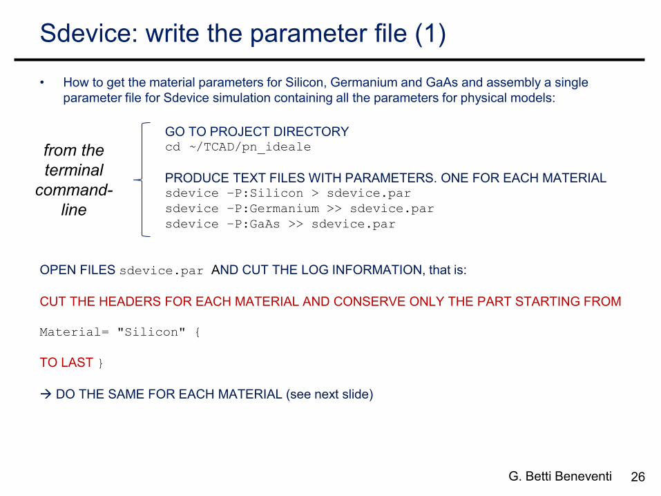
Sdevice: write the parameter file (1)
• How to get the material parameters for Silicon, Germanium and GaAs and assembly a single
parameter file for Sdevice simulation containing all the parameters for physical models:
GO TO PROJECT DIRECTORY cd ~/TCAD/pn_ideale
PRODUCE TEXT FILES WITH PARAMETERS. ONE FOR EACH MATERIAL sdevice –P:Silicon > sdevice.par
sdevice –P:Germanium >> sdevice.par
sdevice –P:GaAs >> sdevice.par
OPEN FILES sdevice.par AND CUT THE LOG INFORMATION, that is:
CUT THE HEADERS FOR EACH MATERIAL AND CONSERVE ONLY THE PART STARTING FROM
Material= "Silicon" {
TO LAST }
DO THE SAME FOR EACH MATERIAL (see next slide)
from the
terminal
command-
line
27 G. Betti Beneventi
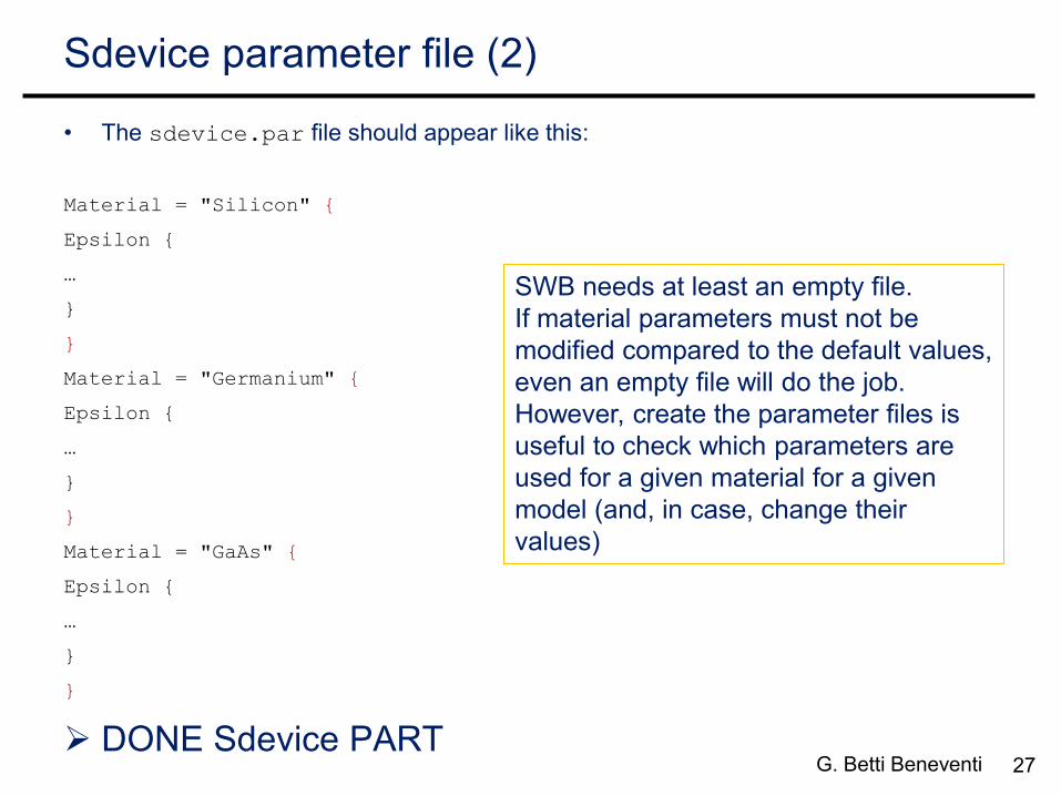
Sdevice parameter file (2)
• The sdevice.par file should appear like this:
Material = "Silicon" {
Epsilon {
…
}
}
Material = "Germanium" {
Epsilon {
…
}
}
Material = "GaAs" {
Epsilon {
…
}
}
DONE Sdevice PART
SWB needs at least an empty file.
If material parameters must not be
modified compared to the default values,
even an empty file will do the job.
However, create the parameter files is
useful to check which parameters are
used for a given material for a given
model (and, in case, change their
values)
28 G. Betti Beneventi
Outline
• Review of basic properties of the diode
• Sentaurus Workbench setup (SWB)
• Implementation of Input files
– Sentaurus Structure Editor (SDE) command file
– Sentaurus Device (SDevice)
• command file
• parameter file
Run the simulation
• Post-processing of results
29 G. Betti Beneventi
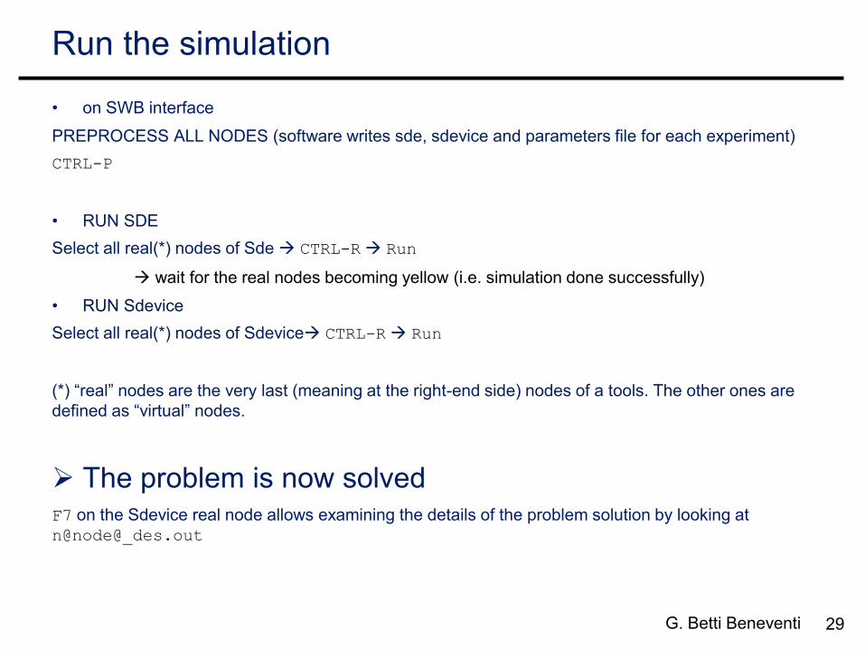
Run the simulation
• on SWB interface
PREPROCESS ALL NODES (software writes sde, sdevice and parameters file for each experiment)
CTRL-P
• RUN SDE
Select all real(*) nodes of Sde CTRL-R Run
wait for the real nodes becoming yellow (i.e. simulation done successfully)
• RUN Sdevice
Select all real(*) nodes of Sdevice CTRL-R Run
(*) “real” nodes are the very last (meaning at the right-end side) nodes of a tools. The other ones are
defined as “virtual” nodes.
The problem is now solved F7 on the Sdevice real node allows examining the details of the problem solution by looking at n@node@_des.out
30 G. Betti Beneventi
Simulation output file
• Select Standard Output to explore:
– Host name (machine used), process ID
– used models and material parameters
– monitoring of the boundary conditions (like bias sweeps)
– information about numerical convergence
Error column:
indication of
convergence.
It is a “normalized”
error indication.
Convergence is
achieved if error is
smaller than one.
The coordinate of
maximum error for
each equation is
also specified
thanks to the use
of the keyword CNormPrint in the
Sdevice command
file. This
information is
particularly useful
in case of non-
convergence, since
it gives indication of
where the
numerical mesh
could need revision
applied voltage total current
saving of .tdr file
relative to the
above voltage
conditions simulation duration
to understand
cause of errors
31 G. Betti Beneventi
Outline
• Review of basic properties of the diode
• Sentaurus Workbench setup (SWB)
• Implementation of Input files
– Sentaurus Structure Editor (SDE) command file
– Sentaurus Device (SDevice)
• command file
• parameter file
• Run the simulation
Post-processing of results
32 G. Betti Beneventi
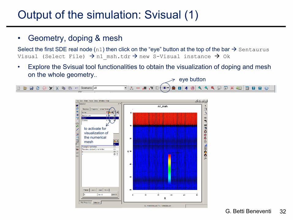
Output of the simulation: Svisual (1)
• Geometry, doping & mesh
Select the first SDE real node (n1) then click on the “eye” button at the top of the bar Sentaurus
Visual (Select File) n1_msh.tdr new S-Visual instance Ok
• Explore the Svisual tool functionalities to obtain the visualization of doping and mesh
on the whole geometry..
to activate for
visualization of
the numerical
mesh
eye button
33 G. Betti Beneventi
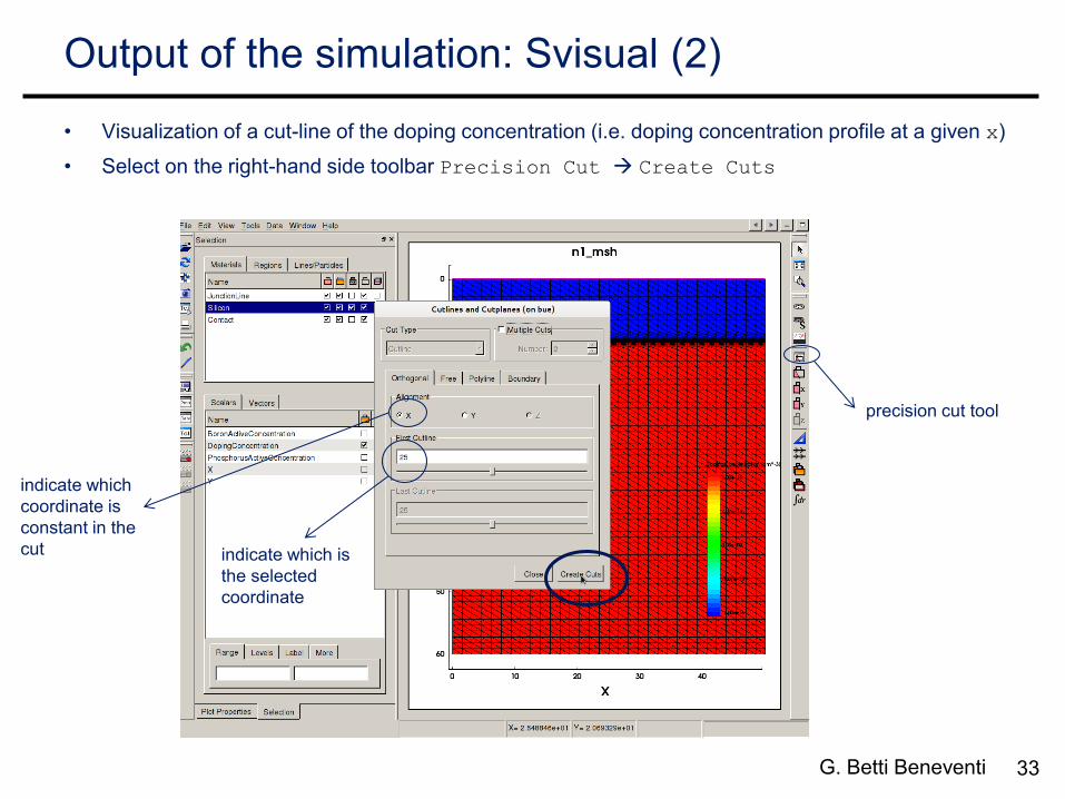
Output of the simulation: Svisual (2)
• Visualization of a cut-line of the doping concentration (i.e. doping concentration profile at a given x)
• Select on the right-hand side toolbar Precision Cut Create Cuts
precision cut tool
indicate which
coordinate is
constant in the
cut indicate which is
the selected
coordinate
34 G. Betti Beneventi
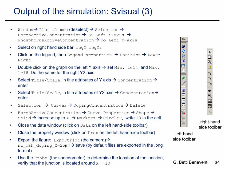
Output of the simulation: Svisual (3)
• Window Plot_n1_msh (deselect) Selection
BoronActiveConcentration To Left Y-Axis
PhosphorusActiveConcentration To Left Y-Axis
• Select on right hand side bar, logY, logY2
• Click on the legend, then Legend properties Position Lower Right
• Double click on the graph on the left Y axis set Min. 1e14 and Max.
1e18. Do the same for the right Y2 axis
• Select Title/Scale, in title attributes of Y axis Concentration
enter
• Select Title/Scale, in title attributes of Y2 axis Concentration
enter
• Selection Curves DopingConcentration Delete
• BoronActiveConcentration Curve Properties Shape
Solid increase up to 4 Markers CircleF, write 10 in the cell
• Close the data window (click on Data on the left hand-side toolbar)
• Close the property window (click on Prop on the left hand-side toolbar)
• Export the figure: ExportPlot (the camera)
n1_msh_doping_X=25mm save (by default files are exported in the .png
format)
• Use the Probe (the speedometer) to determine the location of the junction,
verify that the junction is located around X ~ 10
left-hand
side toolbar
right-hand
side toolbar
35 G. Betti Beneventi
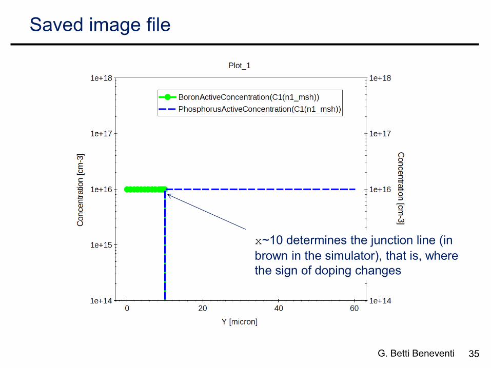
Saved image file
x~10 determines the junction line (in
brown in the simulator), that is, where
the sign of doping changes
36 G. Betti Beneventi
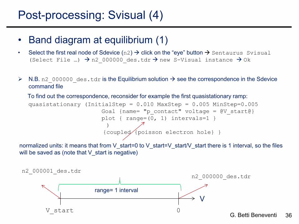
Post-processing: Svisual (4)
• Band diagram at equilibrium (1) • Select the first real node of Sdevice (n2) click on the “eye” button Sentaurus Svisual
(Select File …) n2_000000_des.tdr new S-Visual instance Ok
N.B. n2_000000_des.tdr is the Equilibrium solution see the correspondence in the Sdevice
command file
To find out the correspondence, reconsider for example the first quasistationary ramp:
quasistationary (InitialStep = 0.010 MaxStep = 0.005 MinStep=0.005
Goal {name= "p_contact" voltage = @V_start@}
plot { range=(0, 1) intervals=1 }
)
{coupled {poisson electron hole} }
normalized units: it means that from V_start=0 to V_start=V_start/V_start there is 1 interval, so the files
will be saved as (note that V_start is negative)
V
0 V_start
range= 1 interval
n2_000001_des.tdr n2_000000_des.tdr
37 G. Betti Beneventi
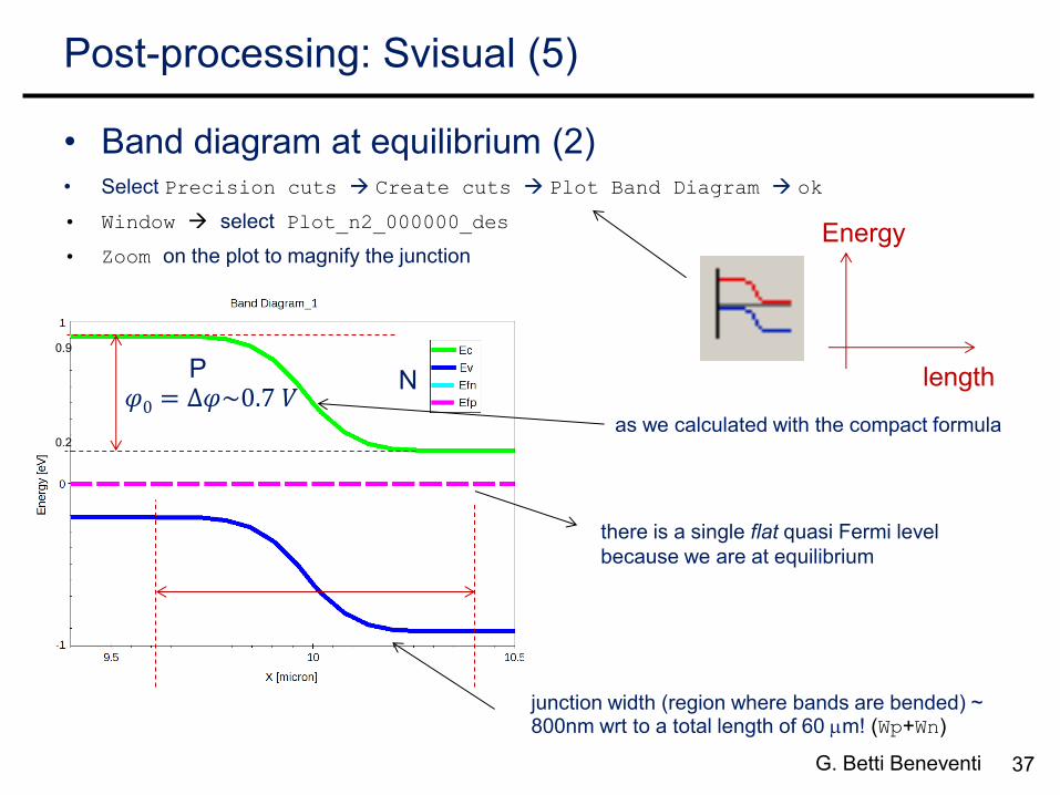
Post-processing: Svisual (5)
• Band diagram at equilibrium (2) • Select Precision cuts Create cuts Plot Band Diagram ok
• Window select Plot_n2_000000_des
• Zoom on the plot to magnify the junction
0.2
𝜑0 = ∆𝜑~0.7 𝑉 as we calculated with the compact formula
junction width (region where bands are bended) ~ 800nm wrt to a total length of 60 mm! (Wp+Wn)
P N
Energy
length
there is a single flat quasi Fermi level
because we are at equilibrium
0.9
38 G. Betti Beneventi
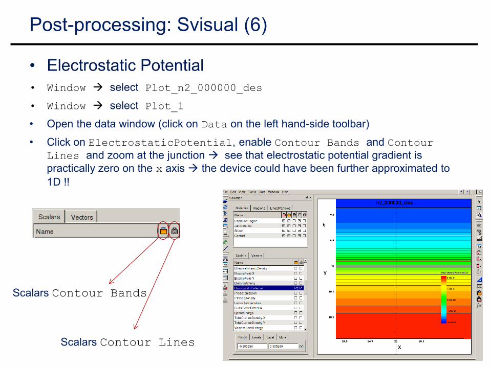
Post-processing: Svisual (6)
• Electrostatic Potential
• Window select Plot_n2_000000_des
• Window select Plot_1
• Open the data window (click on Data on the left hand-side toolbar)
• Click on ElectrostaticPotential, enable Contour Bands and Contour
Lines and zoom at the junction see that electrostatic potential gradient is
practically zero on the x axis the device could have been further approximated to
1D !!
Scalars Contour Lines
Scalars Contour Bands
39 G. Betti Beneventi
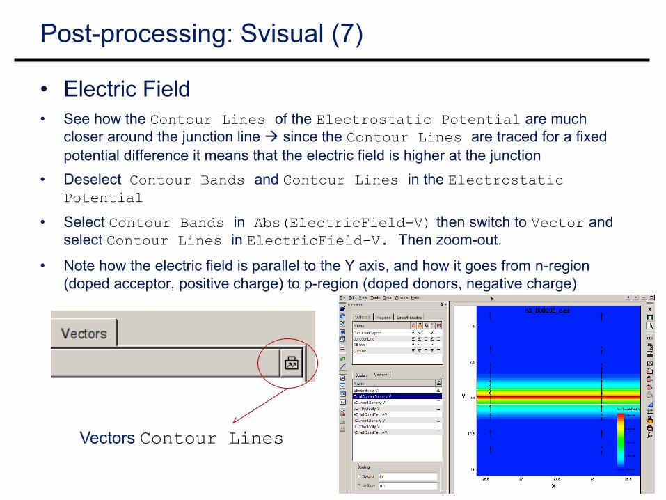
Post-processing: Svisual (7)
• Electric Field
• See how the Contour Lines of the Electrostatic Potential are much
closer around the junction line since the Contour Lines are traced for a fixed
potential difference it means that the electric field is higher at the junction
• Deselect Contour Bands and Contour Lines in the Electrostatic
Potential
• Select Contour Bands in Abs(ElectricField-V) then switch to Vector and
select Contour Lines in ElectricField-V. Then zoom-out.
• Note how the electric field is parallel to the Y axis, and how it goes from n-region
(doped acceptor, positive charge) to p-region (doped donors, negative charge)
Vectors Contour Lines
40 G. Betti Beneventi
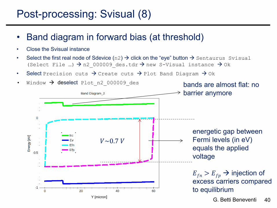
Post-processing: Svisual (8)
• Band diagram in forward bias (at threshold) • Close the Svisual instance
• Select the first real node of Sdevice (n2) click on the “eye” button Sentaurus Svisual
(Select File …) n2_000009_des.tdr new S-Visual instance Ok
• Select Precision cuts Create cuts Plot Band Diagram Ok
• Window deselect Plot_n2_000009_des
energetic gap between
Fermi levels (in eV)
equals the applied
voltage
𝐸𝑓𝑛 > 𝐸𝑓𝑝 injection of
excess carriers compared
to equilibrium
bands are almost flat: no
barrier anymore
𝑉~0.7 𝑉
Y [micron]
41 G. Betti Beneventi
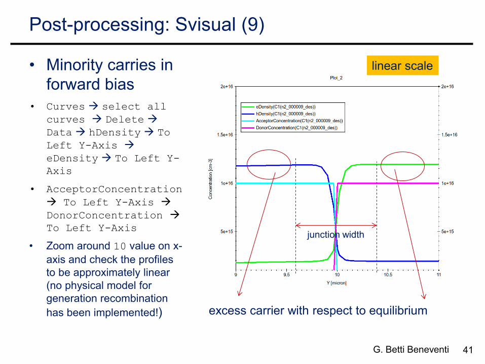
Post-processing: Svisual (9)
• Minority carries in
forward bias
• Curves select all
curves Delete
Data hDensity To
Left Y-Axis
eDensity To Left Y-
Axis
• AcceptorConcentration
To Left Y-Axis
DonorConcentration
To Left Y-Axis
• Zoom around 10 value on x-
axis and check the profiles
to be approximately linear
(no physical model for
generation recombination
has been implemented!)
excess carrier with respect to equilibrium
linear scale
junction width
42 G. Betti Beneventi
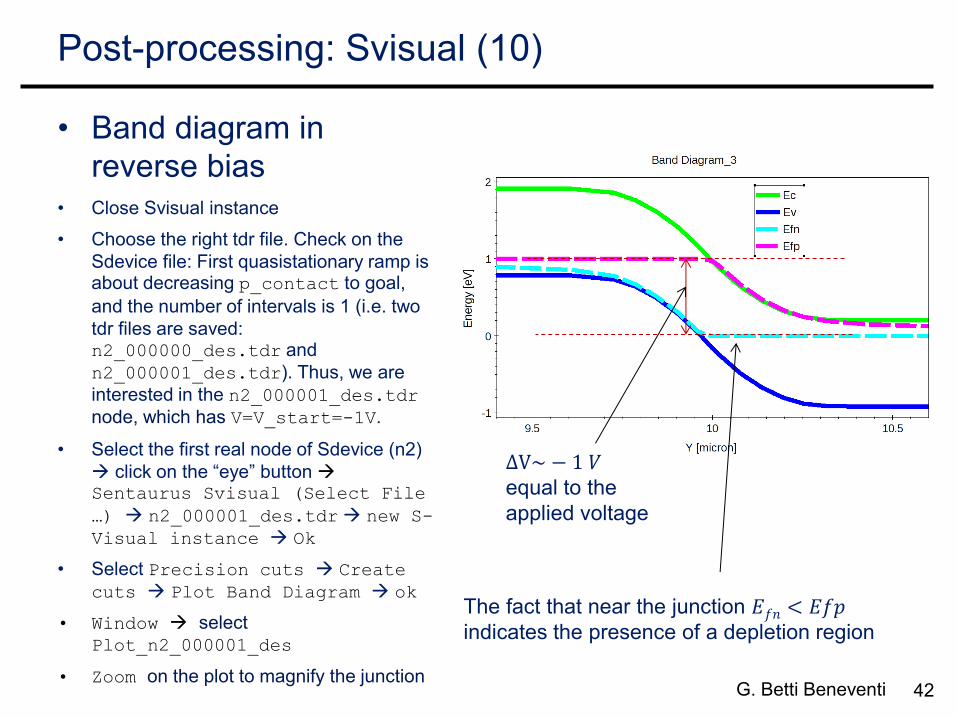
Post-processing: Svisual (10)
• Band diagram in
reverse bias • Close Svisual instance
• Choose the right tdr file. Check on the
Sdevice file: First quasistationary ramp is about decreasing p_contact to goal,
and the number of intervals is 1 (i.e. two
tdr files are saved: n2_000000_des.tdr and
n2_000001_des.tdr). Thus, we are
interested in the n2_000001_des.tdr
node, which has V=V_start=-1V.
• Select the first real node of Sdevice (n2)
click on the “eye” button Sentaurus Svisual (Select File
…) n2_000001_des.tdr new S-
Visual instance Ok
• Select Precision cuts Create
cuts Plot Band Diagram ok
• Window select Plot_n2_000001_des
• Zoom on the plot to magnify the junction
∆V~ − 1 𝑉 equal to the
applied voltage
The fact that near the junction 𝐸𝑓𝑛 < 𝐸𝑓𝑝
indicates the presence of a depletion region
43 G. Betti Beneventi
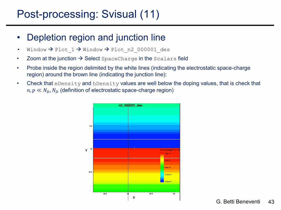
Post-processing: Svisual (11)
• Depletion region and junction line • Window Plot_1 Window Plot_n2_000001_des
• Zoom at the junction Select SpaceCharge in the Scalars field
• Probe inside the region delimited by the white lines (indicating the electrostatic space-charge
region) around the brown line (indicating the junction line):
• Check that eDensity and hDensity values are well below the doping values, that is check that
𝑛, 𝑝 ≪ 𝑁𝐷, 𝑁𝐷 (definition of electrostatic space-charge region)
44 G. Betti Beneventi
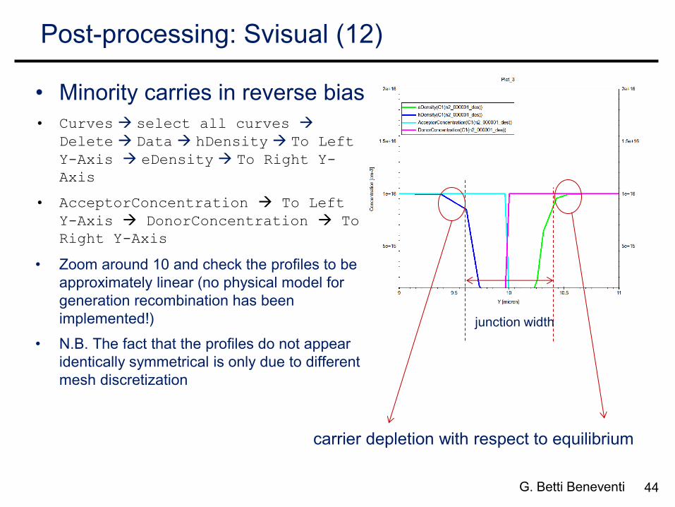
Post-processing: Svisual (12)
• Minority carries in reverse bias
• Curves select all curves
Delete Data hDensity To Left
Y-Axis eDensity To Right Y-
Axis
• AcceptorConcentration To Left
Y-Axis DonorConcentration To
Right Y-Axis
• Zoom around 10 and check the profiles to be
approximately linear (no physical model for
generation recombination has been
implemented!)
• N.B. The fact that the profiles do not appear
identically symmetrical is only due to different
mesh discretization
carrier depletion with respect to equilibrium
junction width
45 G. Betti Beneventi
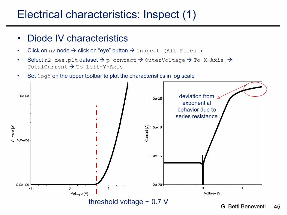
Electrical characteristics: Inspect (1)
• Diode IV characteristics • Click on n2 node click on “eye” button Inspect (All Files…)
• Select n2_des.plt dataset p_contact OuterVoltage To X-Axis
TotalCurrent To Left-Y-Axis
• Set logY on the upper toolbar to plot the characteristics in log scale
threshold voltage ~ 0.7 V
deviation from
exponential
behavior due to
series resistance
46 G. Betti Beneventi
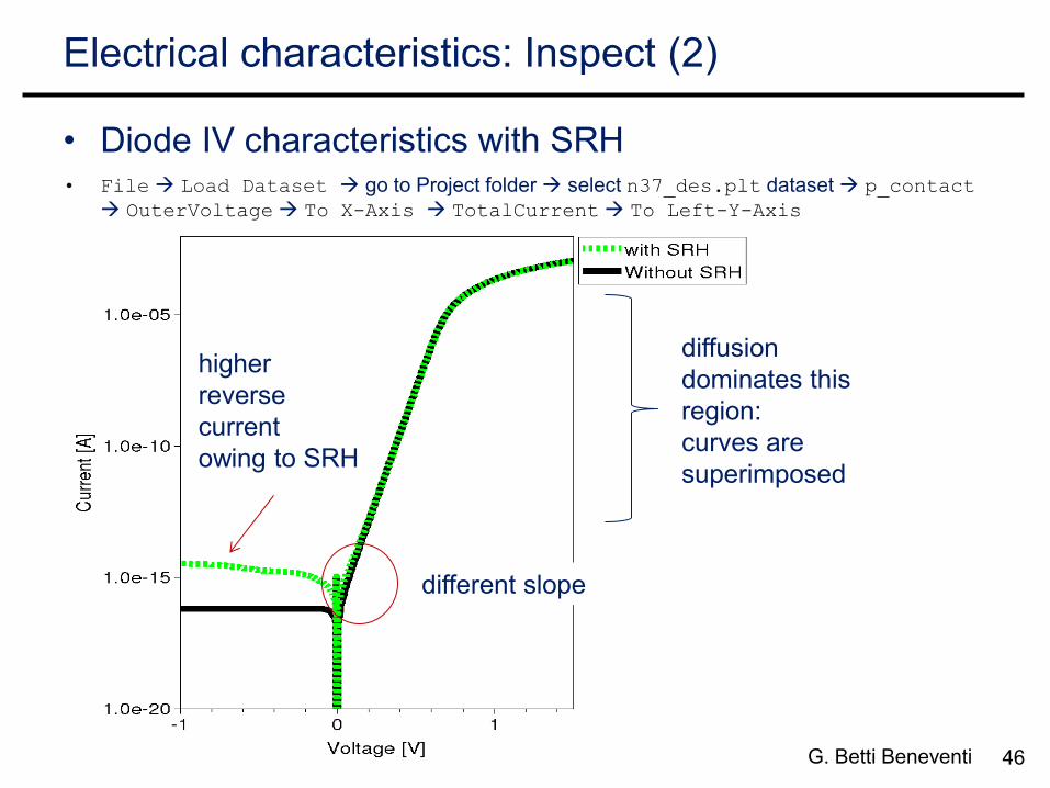
Electrical characteristics: Inspect (2)
• Diode IV characteristics with SRH • File Load Dataset go to Project folder select n37_des.plt dataset p_contact
OuterVoltage To X-Axis TotalCurrent To Left-Y-Axis
different slope
higher
reverse
current
owing to SRH
diffusion
dominates this
region:
curves are
superimposed
47 G. Betti Beneventi
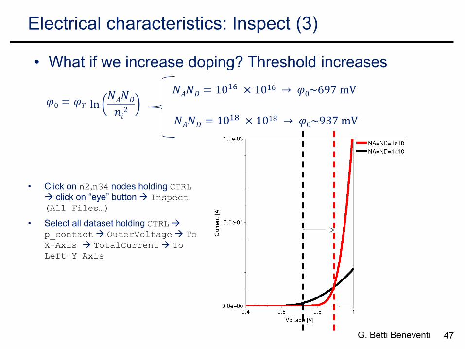
Electrical characteristics: Inspect (3)
• Click on n2,n34 nodes holding CTRL
click on “eye” button Inspect (All Files…)
• Select all dataset holding CTRL
p_contact OuterVoltage To
X-Axis TotalCurrent To Left-Y-Axis
𝜑0 = 𝜑𝑇 ln𝑁𝐴𝑁𝐷
𝑛𝑖2
𝑁𝐴𝑁𝐷 = 1016 × 1016 → 𝜑0~697 mV
𝑁𝐴𝑁𝐷 = 1018 × 1018 → 𝜑0~937 mV
• What if we increase doping? Threshold increases
48 G. Betti Beneventi
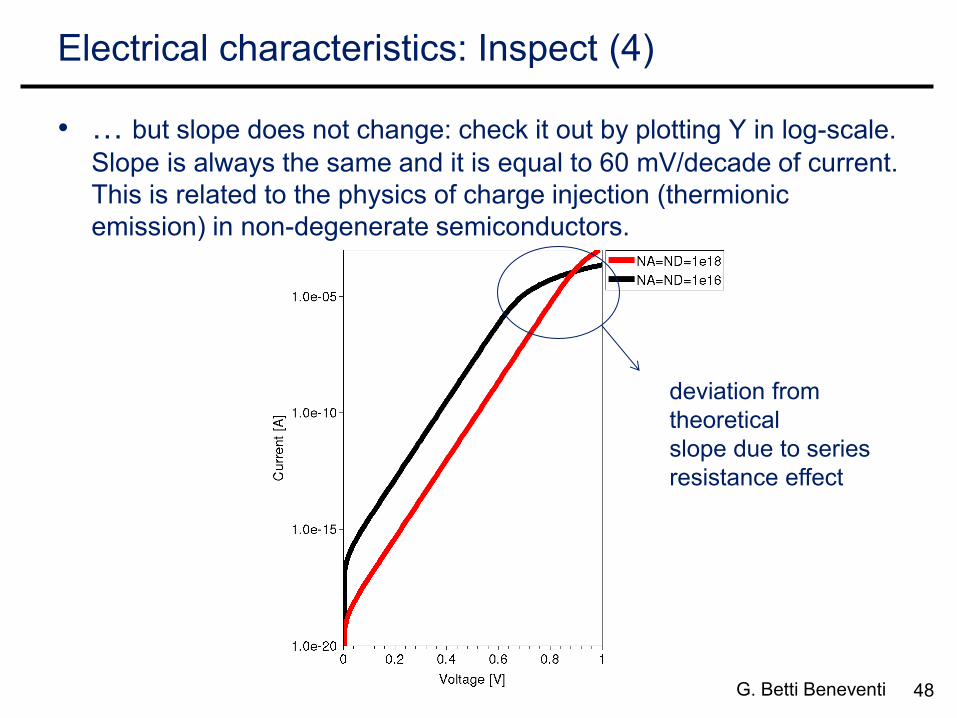
Electrical characteristics: Inspect (4)
• … but slope does not change: check it out by plotting Y in log-scale.
Slope is always the same and it is equal to 60 mV/decade of current.
This is related to the physics of charge injection (thermionic
emission) in non-degenerate semiconductors.
deviation from
theoretical
slope due to series
resistance effect
49 G. Betti Beneventi
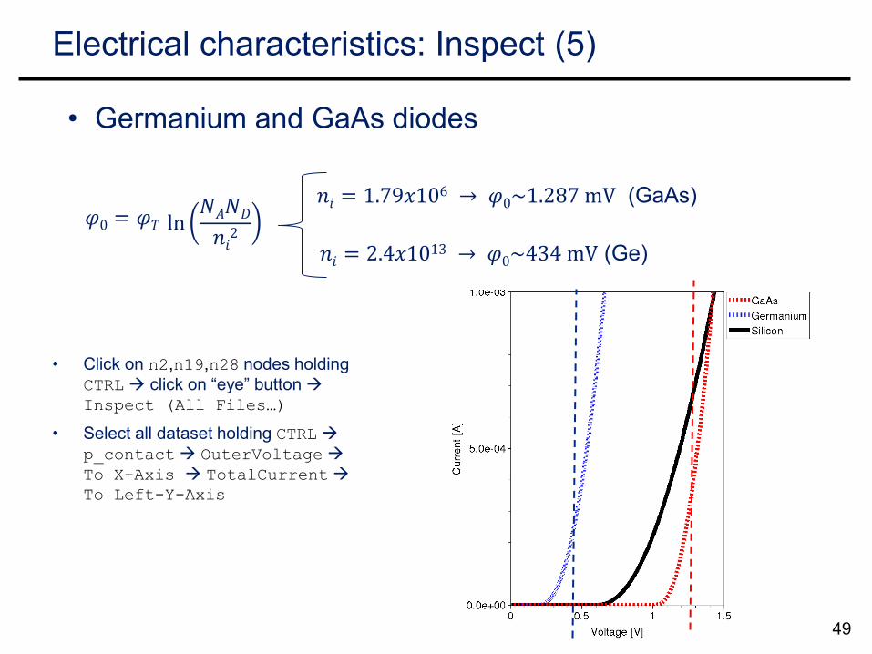
Electrical characteristics: Inspect (5)
• Click on n2,n19,n28 nodes holding
CTRL click on “eye” button Inspect (All Files…)
• Select all dataset holding CTRL
p_contact OuterVoltage
To X-Axis TotalCurrent To Left-Y-Axis
𝜑0 = 𝜑𝑇 ln𝑁𝐴𝑁𝐷
𝑛𝑖2
𝑛𝑖 = 1.79𝑥106 → 𝜑0~1.287 mV (GaAs)
𝑛𝑖 = 2.4𝑥1013 → 𝜑0~434 mV (Ge)
• Germanium and GaAs diodes
50 G. Betti Beneventi
Uniform doping: resistors (1)
• From SWB interface double click on SDE symbol Input Files Edit…
• Go to p-region doping section
• Modify (sdedr:define-constant-profile "p-doping-profile"
BoronActiveConcentration @p_doping@) into(sdedr:define-constant-
profile "p-doping-profile" "@p_doping_type@" @p_doping@)
• From SWB interface, click on p_doping right click Add Parameter
p_doping_type Default value BoronActiveConcentration ok
• Click on n29 node PhosphorusActiveConcentration
• Click on n30 CTRL-R Yes Run
• Click on n34 CTRL-R Run
no junction
anymore,
uniform n-doping
51 G. Betti Beneventi
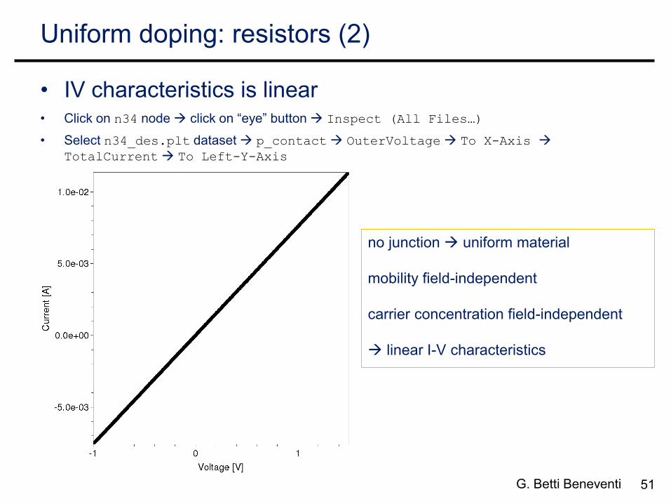
Uniform doping: resistors (2)
• IV characteristics is linear • Click on n34 node click on “eye” button Inspect (All Files…)
• Select n34_des.plt dataset p_contact OuterVoltage To X-Axis
TotalCurrent To Left-Y-Axis
no junction uniform material
mobility field-independent
carrier concentration field-independent
linear I-V characteristics
52 G. Betti Beneventi
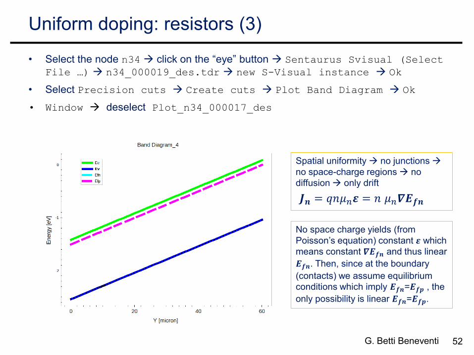
Uniform doping: resistors (3)
• Select the node n34 click on the “eye” button Sentaurus Svisual (Select
File …) n34_000019_des.tdr new S-Visual instance Ok
• Select Precision cuts Create cuts Plot Band Diagram Ok
• Window deselect Plot_n34_000017_des
No space charge yields (from
Poisson’s equation) constant 𝜺 which
means constant 𝜵𝑬𝒇𝒏 and thus linear
𝑬𝒇𝒏. Then, since at the boundary
(contacts) we assume equilibrium
conditions which imply 𝑬𝒇𝒏=𝑬𝒇𝒑 , the
only possibility is linear 𝑬𝒇𝒏=𝑬𝒇𝒑.
𝑱𝒏 = 𝑞𝑛𝜇𝑛𝜺 = 𝑛 𝜇𝑛𝜵𝑬𝒇𝒏
Spatial uniformity no junctions
no space-charge regions no
diffusion only drift
53 G. Betti Beneventi
Bibliography
• J.M. Rabaey, A. Chandrakasan, B. Nikolic, Digitial Integrated Circuits: A Design
Perspective, Prentice Hall, 2003.
• Giovanni Ghione, Dispositivi per la Microelettronica, McGraw-Hill, 1998.
• Sentaurus Synopys User’s guides
Related Documents


![VARI: CERVENKAetal.: TCAD SIMULATION OF … · The 143 process simulations have been set up in Sentaurus Workbench (SWB) of the TCAD simulation package of SYN-OPSYS [3].](https://static.cupdf.com/doc/110x72/5b5687f07f8b9a022e8c9fb2/vari-cervenkaetal-tcad-simulation-of-the-143-process-simulations-have-been.jpg)


![TCAD for reliability - Semantic Scholar · PDF fileTCAD for reliability ... opsys Sentaurus TCAD [1], are well established for modeling semi-conductor fabrication process, and device](https://static.cupdf.com/doc/110x72/5a9cd7257f8b9aba4a8e7433/tcad-for-reliability-semantic-scholar-for-reliability-opsys-sentaurus-tcad.jpg)