IEEE TRANSACTIONS ON CIRCUITS AND SYSTEMS—I: REGULAR PAPERS, VOL. 55, NO. 2, MARCH 2008 687 Switched-Capacitor/Switched-Inductor Structures for Getting Transformerless Hybrid DC–DC PWM Converters Boris Axelrod, Yefim Berkovich, Member, IEEE, and Adrian Ioinovici, Fellow, IEEE Abstract—A few simple switching structures, formed by either two capacitors and two-three diodes (C-switching), or two in- ductors and two-three diodes (L-switching) are proposed. These structures can be of two types: “step-down” and “step-up.” These blocks are inserted in classical converters: buck, boost, buck–boost, C ´ uk, Zeta, Sepic. The “step-down” C- or L-switching structures can be combined with the buck, buck–boost, C ´ uk, Zeta, Sepic converters in order to get a step-down function. When the active switch of the converter is on, the inductors in the L-switching blocks are charged in series or the capacitors in the C-switching blocks are discharged in parallel. When the active switch is off, the inductors in the L-switching blocks are discharged in parallel or the capacitors in the C-switching blocks are charged in series. The “step-up” C- or L-switching structures are combined with the boost, buck–boost, C ´ uk, Zeta, Sepic converters, to get a step-up function. The steady-state analysis of the new hybrid converters allows for determing their dc line-to-output voltage ratio. The gain formula shows that the hybrid converters are able to reduce/increase the line voltage more times than the original, classical converters. The proposed hybrid converters contain the same number of elements as the quadratic converters. Their performances (dc gain, voltage and current stresses on the active switch and diodes, currents through the inductors) are compared to those of the available quadratic converters. The superiority of the new, hybrid converters is mainly based on less energy in the magnetic field, leading to saving in the size and cost of the inductors, and less current stresses in the switching elements, leading to smaller conduction losses. Experimental results confirm the theoretical analysis. Index Terms—DC–DC hybrid converter, switched capacitor, switched inductor, steady-state analysis. I. INTRODUCTION T HE basic dc–dc converters, buck (whose ideal line-to- output voltage ratio is being the duty cycle), boost , buck–boost, C ´ uk, Sepic, and Zeta can not provide a steep step-down, respectively step-up of the line voltage, as required by many modern applications. The today integrated circuits (ICs) are drawing their power from less than 5-V power supplies. It is estimated that the supply voltage for future microprocessors Manuscript received August 15, 2005; revised January 13, 2006. This paper was presented in part at the International Symposium on Circuits and Systems, Kobe, Japan, May 23–26, 2005, and at the International Symposium on Circuits and Systems, Kos Island, Greece, May 21–24, 2006. This paper was recom- mended by Associate Editor M. K. Kazimierczuk. The authors are with Holon Institute of Technology, Holon 58102, Israel (e-mail: [email protected]). Digital Object Identifier 10.1109/TCSI.2008.916403 will decrease from 3.5 to 1 V, and even lower, in order to decrease the power loss of modern high power consumption CPUs [1]. Power supplies able to reduce the standard voltage of 12 V (or 48 V) to about 1 V are necessary [1]. When using telecom standard equipment for providing Internet services, the 48 V of the dc battery plant has to be boosted to a 380-V intermediate dc bus [3]. The high intensity discharge lamps (HID) for automobile head lamps require at their start-up the increase of the voltage from the battery’s 12 V to more then 100 V, at 35-W power [3]. In order to provide such a high voltage-conversion ratio , the basic converters would have to operate with an extreme value of the duty cycle, smaller than 0.1 in voltage-step-down converters, higher than 0.9 in voltage-step-up converters. An extreme duty cycle impairs the efficiency and imposes obstacles for the transient response [4]. Also, to generate such an extreme duty cycle, the control circuit must incorporate a very fast, ex- pensive comparator. The extreme duty cycle may even cause malfunctions at high switching frequency due to the very short conduction time of the diode (self-driven transistor) in step-up converters, or of the active transistor in step-down converters. An obvious solution would be the use of transformers to get the desired voltage conversion ratio, like in forward or flyback converters. However, if the industrial application does not require for dc isolation, the use of a transformer would only increase the cost, the volume, and the losses. Moreover, a large transformer turns ratio would increase the voltage stress on the primary elements, impossing a heavy penalty on the efficiency. Voltage regulators have recently been developed for getting a sub-1-V supply voltage needed in microprocessors [5]. These converters, purposely designed for high load current and fast dynamics, are still in the development phase for answering the tough requirements. The switched-capacitor converters, proposed in the 1990’s, can provide any steep conversion ratio (a tutorial on these cir- cuits can be found in [6]). However, they operate with a rela- tively low efficiency, and put challenges in the charging path of the capacitors. Use of cascade of converters for getting the desired voltage ratio is a no-solution in the today’s energy-saving conscious world, as this procedure implies an overall efficiency equal to the product of the efficiencies of each circuit. Quadratic converters can somehow alleviate the efficiency problem of cascade circuits by using a single driven transistor [7], [8], but they may present voltage or current overstresses. 1549-8328/$25.00 © 2008 IEEE Authorized licensed use limited to: Politehnica Timisoara. Downloaded on January 16, 2010 at 08:08 from IEEE Xplore. Restrictions apply.

Welcome message from author
This document is posted to help you gain knowledge. Please leave a comment to let me know what you think about it! Share it to your friends and learn new things together.
Transcript
IEEE TRANSACTIONS ON CIRCUITS AND SYSTEMS—I: REGULAR PAPERS, VOL. 55, NO. 2, MARCH 2008 687
Switched-Capacitor/Switched-InductorStructures for Getting Transformerless
Hybrid DC–DC PWM ConvertersBoris Axelrod, Yefim Berkovich, Member, IEEE, and Adrian Ioinovici, Fellow, IEEE
Abstract—A few simple switching structures, formed by eithertwo capacitors and two-three diodes (C-switching), or two in-ductors and two-three diodes (L-switching) are proposed. Thesestructures can be of two types: “step-down” and “step-up.”These blocks are inserted in classical converters: buck, boost,buck–boost, Cuk, Zeta, Sepic. The “step-down” C- or L-switchingstructures can be combined with the buck, buck–boost, Cuk,Zeta, Sepic converters in order to get a step-down function. Whenthe active switch of the converter is on, the inductors in theL-switching blocks are charged in series or the capacitors in theC-switching blocks are discharged in parallel. When the activeswitch is off, the inductors in the L-switching blocks are dischargedin parallel or the capacitors in the C-switching blocks are chargedin series. The “step-up” C- or L-switching structures are combinedwith the boost, buck–boost, Cuk, Zeta, Sepic converters, to geta step-up function. The steady-state analysis of the new hybridconverters allows for determing their dc line-to-output voltageratio. The gain formula shows that the hybrid converters are ableto reduce/increase the line voltage more times than the original,classical converters. The proposed hybrid converters containthe same number of elements as the quadratic converters. Theirperformances (dc gain, voltage and current stresses on the activeswitch and diodes, currents through the inductors) are comparedto those of the available quadratic converters. The superiorityof the new, hybrid converters is mainly based on less energy inthe magnetic field, leading to saving in the size and cost of theinductors, and less current stresses in the switching elements,leading to smaller conduction losses. Experimental results confirmthe theoretical analysis.
Index Terms—DC–DC hybrid converter, switched capacitor,switched inductor, steady-state analysis.
I. INTRODUCTION
THE basic dc–dc converters, buck (whose ideal line-to-output voltage ratio is being the duty
cycle), boost , buck–boost, Cuk, Sepic, andZeta can not provide a steep step-down,respectively step-up of the line voltage, as required by manymodern applications. The today integrated circuits (ICs) aredrawing their power from less than 5-V power supplies. It isestimated that the supply voltage for future microprocessors
Manuscript received August 15, 2005; revised January 13, 2006. This paperwas presented in part at the International Symposium on Circuits and Systems,Kobe, Japan, May 23–26, 2005, and at the International Symposium on Circuitsand Systems, Kos Island, Greece, May 21–24, 2006. This paper was recom-mended by Associate Editor M. K. Kazimierczuk.
The authors are with Holon Institute of Technology, Holon 58102, Israel(e-mail: [email protected]).
Digital Object Identifier 10.1109/TCSI.2008.916403
will decrease from 3.5 to 1 V, and even lower, in order todecrease the power loss of modern high power consumptionCPUs [1]. Power supplies able to reduce the standard voltageof 12 V (or 48 V) to about 1 V are necessary [1]. When usingtelecom standard equipment for providing Internet services,the 48 V of the dc battery plant has to be boosted to a 380-Vintermediate dc bus [3]. The high intensity discharge lamps(HID) for automobile head lamps require at their start-up theincrease of the voltage from the battery’s 12 V to more then100 V, at 35-W power [3].
In order to provide such a high voltage-conversion ratio ,the basic converters would have to operate with an extremevalue of the duty cycle, smaller than 0.1 in voltage-step-downconverters, higher than 0.9 in voltage-step-up converters. Anextreme duty cycle impairs the efficiency and imposes obstaclesfor the transient response [4]. Also, to generate such an extremeduty cycle, the control circuit must incorporate a very fast, ex-pensive comparator. The extreme duty cycle may even causemalfunctions at high switching frequency due to the very shortconduction time of the diode (self-driven transistor) in step-upconverters, or of the active transistor in step-down converters.
An obvious solution would be the use of transformers toget the desired voltage conversion ratio, like in forward orflyback converters. However, if the industrial application doesnot require for dc isolation, the use of a transformer wouldonly increase the cost, the volume, and the losses. Moreover, alarge transformer turns ratio would increase the voltagestress on the primary elements, impossing a heavy penalty onthe efficiency.
Voltage regulators have recently been developed for gettinga sub-1-V supply voltage needed in microprocessors [5]. Theseconverters, purposely designed for high load current and fastdynamics, are still in the development phase for answering thetough requirements.
The switched-capacitor converters, proposed in the 1990’s,can provide any steep conversion ratio (a tutorial on these cir-cuits can be found in [6]). However, they operate with a rela-tively low efficiency, and put challenges in the chargingpath of the capacitors.
Use of cascade of converters for getting the desired voltageratio is a no-solution in the today’s energy-saving consciousworld, as this procedure implies an overall efficiency equal tothe product of the efficiencies of each circuit.
Quadratic converters can somehow alleviate the efficiencyproblem of cascade circuits by using a single driven transistor[7], [8], but they may present voltage or current overstresses.
1549-8328/$25.00 © 2008 IEEE
Authorized licensed use limited to: Politehnica Timisoara. Downloaded on January 16, 2010 at 08:08 from IEEE Xplore. Restrictions apply.
688 IEEE TRANSACTIONS ON CIRCUITS AND SYSTEMS—I: REGULAR PAPERS, VOL. 55, NO. 2, MARCH 2008
Starting from the switched-capacitor cells, switched inductor-capacitor circuits have been developed in [9].
A systematic, topological-based way of designing new struc-tures of converters, was proposed for the first time in [10]. Usingthe duality between a switching-capacitor cell and a switching-inductor cell, as well as the duality between a voltage-drivenconverters and a current-driven one, new converters have beenproposed. General topological formulas allowed for calculatingthe voltage ratio of each converter. However, [10] limits itself topower supplies containing maximum two switches, and are notnecessarily providers of large conversion ratios.
One structure allowing only a high step-up of the line, usingthose switches is given in [11], it contains a capacitor-diodevoltage multiplier, similar to the multistage capacitor dividerused in [12] for getting large step down voltage ratios. Thesesingular schemes can provide large ratios, but they are accom-panied by the inherent disadvantages of the switched-capacitorcircuits [6].
A new approach is proposed in this paper: simple switchingdual structures, formed by either two capacitors and 2–3diodes, or two inductors and 2–3 diodes are defined. Thesecircuit blocks can provide either a step-down of the inputvoltage or a step-up of it. They are inserted in classical buck,boost, buck–boost, Cuk, Sepic, Zeta converters to providenew power supplies with a steep voltage conversion ratio. Astheir complexity in terms of circuit elements is comparable tothat of the quadratic converters, their performances (voltageratio, stresses, efficiency) will be compared to that of availablequadratic circuits.
The step-down and step-up switching-capacitor/switching in-ductor structures will be presented in Section II. The realiza-tion of new hybrid, transformerless dc–dc pulsewidth-modu-lated (PWM) converters will be aim of Section III, where anapproximate dc analysis (losses neglected) will be performedto get the voltage conversion ratio for each new circuit. One ofthe new converters, the hybrid Cuk converter, was implementedin the laboratory and the experimental results will be shown inSection IV. Section V will be devoted to a comparison of thenew hybrid converters and with the quadratic ones. Conclusionswill end the paper.
II. SWITCHED CAPACITOR/SWITCHED INDUCTOR
STEP-DOWN/STEP-UP STRUCTURES
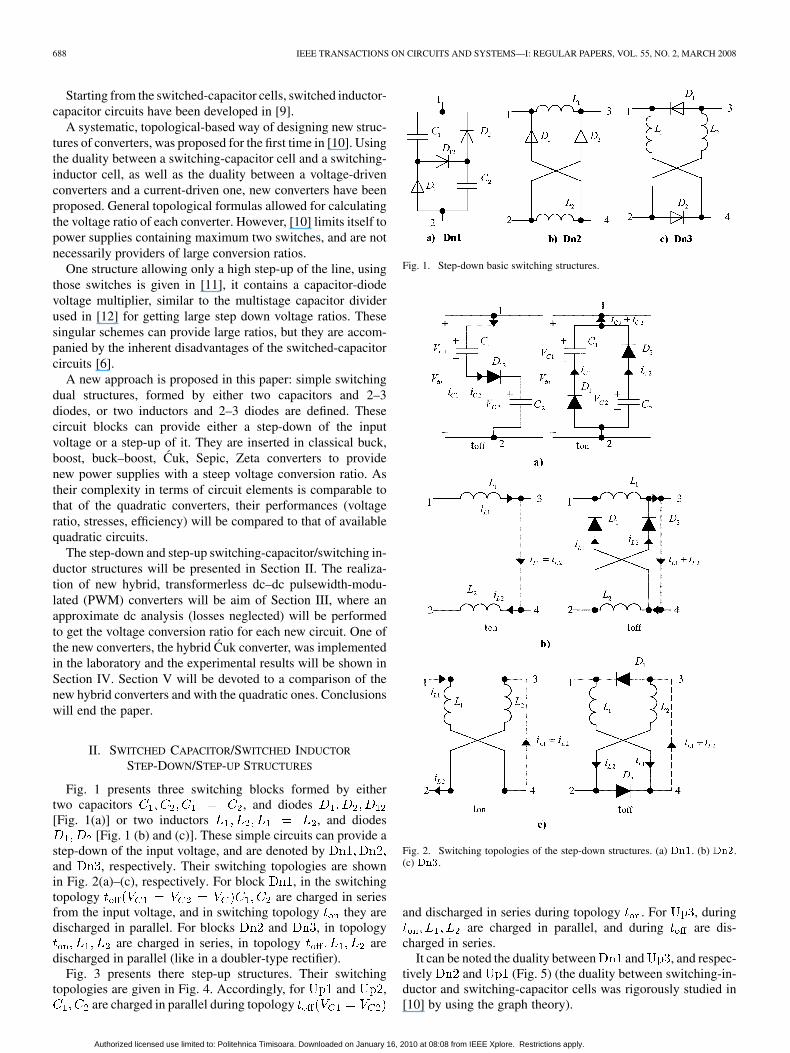
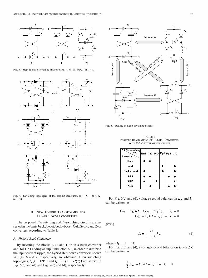
Fig. 1 presents three switching blocks formed by eithertwo capacitors , and diodes[Fig. 1(a)] or two inductors , and diodes
[Fig. 1 (b) and (c)]. These simple circuits can provide astep-down of the input voltage, and are denoted byand , respectively. Their switching topologies are shownin Fig. 2(a)–(c), respectively. For block , in the switchingtopology are charged in seriesfrom the input voltage, and in switching topology they aredischarged in parallel. For blocks and , in topology
are charged in series, in topology aredischarged in parallel (like in a doubler-type rectifier).
Fig. 3 presents there step-up structures. Their switchingtopologies are given in Fig. 4. Accordingly, for and ,
are charged in parallel during topology
Fig. 1. Step-down basic switching structures.
Fig. 2. Switching topologies of the step-down structures. (a) Dn1. (b) Dn2.(c) Dn3.
and discharged in series during topology . For , duringare charged in parallel, and during are dis-
charged in series.It can be noted the duality between and , and respec-
tively and (Fig. 5) (the duality between switching-in-ductor and switching-capacitor cells was rigorously studied in[10] by using the graph theory).
Authorized licensed use limited to: Politehnica Timisoara. Downloaded on January 16, 2010 at 08:08 from IEEE Xplore. Restrictions apply.
AXELROD et al.: SWITCHED-CAPACITOR/SWITCHED-INDUCTOR STRUCTURES 689
Fig. 3. Step-up basic switching structures. (a) Up1. (b) Up2. (c) Up3.
Fig. 4. Switching topologies of the step-up structures. (a) Up1. (b) Up2.(c) Up3.
III. NEW HYBRID TRANSFORMERLESS
DC–DC PWM CONVERTERS
The proposed -switching and -switching circuits are in-serted in the basic buck, boost, buck–boost, Cuk, Sepic, and Zetaconverters according to Table I.
A. Hybrid Buck Converter.
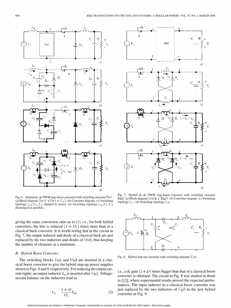
By inserting the blocks and in a buck converterand, for adding an input inductor, , in order to diminishthe input current ripple, the hybrid step-down converters shownin Figs. 6 and 7, respectively, are obtained. Their switchingtopologies, and are shown inFig. 6(c) and (d) and Fig. 7(c) and (d), respectively.
Fig. 5. Duality of basic switching blocks.
TABLE IPOSSIBLE REALIZATIONS OF HYBRID CONVERTERS
WITH C-/L-SWITCHING STRUCTURES
For Fig. 6(c) and (d), voltage-second balances on andcan be written as
giving
(1)
where .For Fig. 7(c) and (d), a voltage-second balance on (or )
can be written as
Authorized licensed use limited to: Politehnica Timisoara. Downloaded on January 16, 2010 at 08:08 from IEEE Xplore. Restrictions apply.
690 IEEE TRANSACTIONS ON CIRCUITS AND SYSTEMS—I: REGULAR PAPERS, VOL. 55, NO. 2, MARCH 2008
Fig. 6. Hybrid dc–dc PWM step-down converter with switching structureDn1.(a) Block diagram (buck+Dn1+L ). (b) Converter diagram. (c) Switchingtopology t (C ;C charged in series). (d) Switching topology t (C ;Cdischarged in parallel).
giving the same conversion ratio as in (1), i.e., for both hybridconverters, the line is reduced times more than in aclassical buck converter. It is worth noting that in the circuit inFig. 7, the output inductor and diode of a classical buck are justreplaced by the two inductors and diodes of , thus keepingthe number of elements at a minimum.
B. Hybrid Boost Converter
The switching blocks and are inserted in a clas-sical boost converter to give the hybrid step-up power suppliesshown in Figs. 8 and 9, respectively. For reducing the output cur-rent ripple, an output inductor is inserted after . Voltage-second balance on the inductors lead to
(2)
Fig. 7. Hybrid dc–dc PWM step-down converter with switching structureDn2. (a) Block diagram (buck +Dn2). (b) Converter diagram. (c) Switchingtopology t . (d) Switching topology t .
Fig. 8. Hybrid step-up converter with switching structure Up1.
i.e., a dc gain times bigger than that of a classical boostconverter is obtained. The circuit in Fig. 8 was studied in detailin [13], where experimental results proved the expected perfor-mances. The input inductor in a classical boost converter wasjust replaced by the two inductors of in the new hybridconverter in Fig. 9.
Authorized licensed use limited to: Politehnica Timisoara. Downloaded on January 16, 2010 at 08:08 from IEEE Xplore. Restrictions apply.
AXELROD et al.: SWITCHED-CAPACITOR/SWITCHED-INDUCTOR STRUCTURES 691
Fig. 9. Hybrid step-up converter with switching structure Up3.
Fig. 10. Hybrid buck–boost converter in step-down mode.
Fig. 11. Hybrid buck–boost converter in step-up mode using Up1.
C. Hybrid Buck–Boost Converter
As shown in Table I, three buck–boost type hybrid converterscan be obtained: for a step-down operation, is inserted as inFig. 10. An input inductor is added to smooth the input currentripple (i.e., together with the capacitors of the blockact as a low-pass filter). For a step-up operation, the switchingblocks , are inserted as in Figs. 11 and 12, respectively.
From the switching topologies of the converter shownin Fig. 10, one gets the voltage balance equations on and ,which lead to
(3)
i.e., the line-to-load ratio is reduced times more thanin a classical buck–boost converter.
Similarly, for the converters in Figs. 11 and 12, one gets
(4)
Fig. 12. Hybrid buck–boost converter in step-up mode using Up3.
Fig. 13. Hybrid Cuk converter in step-down mode using Dn1.
Fig. 14. Hybrid Cuk converter in step-down mode using Dn2.
i.e., the double of the conversion ratio of the classicalbuck–boost converter. In the hybrid converter shown inFig. 12, the inductor of a classical buck–boost converter is justreplaced by the two inductors, of , thus minimizing thenumber of elements.
D. Hybrid Cuk Converter
Four new converters can be constructed by inserting eitherthe step-down switching blocks , , or step-up switchingstructures , in a classical Cuk converter (Figs. 13–16).
In the converter shown in Fig. 13, the input capacitor of theclassical Cuk converter is not necessary, and in Fig. 14 theoutput diode and inductor in a classical Cuk converter are notnecessary.
The voltage-second balance equations on the inductors leadto
(5)
i.e., a step-down two times steeper than that provided by theclassical Cuk converter is obtained.
Authorized licensed use limited to: Politehnica Timisoara. Downloaded on January 16, 2010 at 08:08 from IEEE Xplore. Restrictions apply.

692 IEEE TRANSACTIONS ON CIRCUITS AND SYSTEMS—I: REGULAR PAPERS, VOL. 55, NO. 2, MARCH 2008
Fig. 15. Hybrid Cuk converter in step-up mode, using Up2. (a) block diagram(Cuk+Up2). (b) Converter diagram. (c) Switching topology t (L charged,C ;C discharged in series). (d) Switching topology t (L discharged,C ;C charged in parallel).
For the step-up converters, the input capacitor of a classicalCuk converter becomes redundant if block is used (Fig. 15)and the input inductor becomes unnecessary if block isused (Fig. 16), thus saving one passive element.
The voltage balances on and in Fig. 15 (c) and (d)gives
giving
(6)
Fig. 16. Hybrid Cuk converter in step-up mode using Up3. (a) block diagram(Cuk+Up3). (b) Converter diagram. (c) Switching topology t ; (L ;Lcharged in parallel, L charged). (d) Switching topology t ((L ;L dis-charged in series, L discharged).
The voltage balance on and in Fig. 16 (c) and (d) gives
resulting in
(7)
i.e., a step-up times more than in a classical Cuk con-verter is obtained.
Authorized licensed use limited to: Politehnica Timisoara. Downloaded on January 16, 2010 at 08:08 from IEEE Xplore. Restrictions apply.
AXELROD et al.: SWITCHED-CAPACITOR/SWITCHED-INDUCTOR STRUCTURES 693
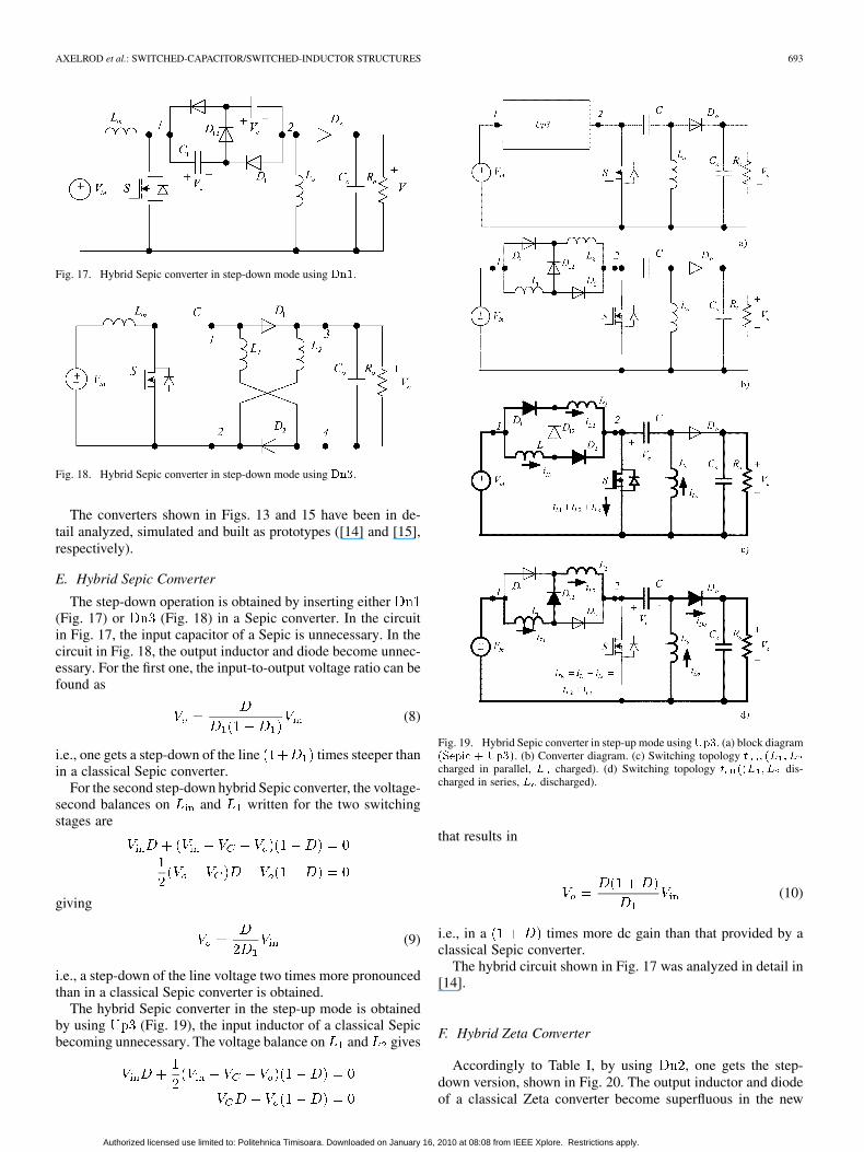
Fig. 17. Hybrid Sepic converter in step-down mode using Dn1.
Fig. 18. Hybrid Sepic converter in step-down mode using Dn3.
The converters shown in Figs. 13 and 15 have been in de-tail analyzed, simulated and built as prototypes ([14] and [15],respectively).
E. Hybrid Sepic Converter
The step-down operation is obtained by inserting either(Fig. 17) or (Fig. 18) in a Sepic converter. In the circuitin Fig. 17, the input capacitor of a Sepic is unnecessary. In thecircuit in Fig. 18, the output inductor and diode become unnec-essary. For the first one, the input-to-output voltage ratio can befound as
(8)
i.e., one gets a step-down of the line times steeper thanin a classical Sepic converter.
For the second step-down hybrid Sepic converter, the voltage-second balances on and written for the two switchingstages are
giving
(9)
i.e., a step-down of the line voltage two times more pronouncedthan in a classical Sepic converter is obtained.
The hybrid Sepic converter in the step-up mode is obtainedby using (Fig. 19), the input inductor of a classical Sepicbecoming unnecessary. The voltage balance on and gives
Fig. 19. Hybrid Sepic converter in step-up mode using Up3. (a) block diagram(Sepic + Up3). (b) Converter diagram. (c) Switching topology t ; (L ;L
charged in parallel, L charged). (d) Switching topology t ((L ;L dis-charged in series, L discharged).
that results in
(10)
i.e., in a times more dc gain than that provided by aclassical Sepic converter.
The hybrid circuit shown in Fig. 17 was analyzed in detail in[14].
F. Hybrid Zeta Converter
Accordingly to Table I, by using , one gets the step-down version, shown in Fig. 20. The output inductor and diodeof a classical Zeta converter become superfluous in the new
Authorized licensed use limited to: Politehnica Timisoara. Downloaded on January 16, 2010 at 08:08 from IEEE Xplore. Restrictions apply.

694 IEEE TRANSACTIONS ON CIRCUITS AND SYSTEMS—I: REGULAR PAPERS, VOL. 55, NO. 2, MARCH 2008
Fig. 20. Hybrid Zeta converter in step-down mode using Dn2.
Fig. 21. Hybrid Zeta converter in step-up mode using Up2.
Fig. 22. Hybrid Zeta converter in step-up mode using Up3.
power supply. From the voltage balance equations on andwritten for the two switching stages, one gets
(11)
which shows a two times steeper reduction of the line comparedwith the performance of a classical Zeta converter.
Two step-up hybrid Zeta power supplies are obtained by in-serting (Fig. 21), in which case the input capacitor of a Zetaconverter becomes unnecessary, or (Fig. 22), in which casethe input inductor of a Zeta converter becomes superfluous. Forthe two converters, one gets, respectively
(12)
(13)
Therefore, the new power supplies offer an output voltagedouble, and respectively times larger than that providedby a Zeta converter for the same line.
Fig. 23. Experimental voltage waveforms of the hybrid Cuk converter withDn1.
Fig. 24. Experimental voltage waveforms of the hybrid Cuk converter withUp2.
IV. EXPERIMENTAL RESULTS
The hybrid Cuk converter with the step-down switching block(Fig. 13) was implemented in the laboratory. The experi-
mental results are given in Fig. 23. The circuit parameters wereas follows:
V W H H
kHz. The switchwas a MOSFET IRF 540 and , were diodesMBR 1640.
The hybrid Cuk converter with the step-up switching blockUp2 (Fig. 15) and with the same circuit parameters and
was also built and tested. The experimental results aregiven in Fig. 24, they agree with the theoretical analysis.
V. COMPARISON OF PROPOSED CONVERTERS
WITH QUADRATIC CONVERTERS I [7]
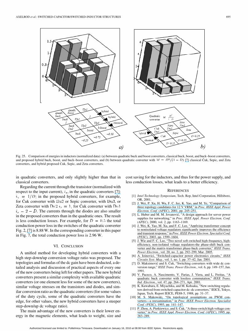
As the number of elements and voltage stresses across thetransistor and diodes are similar for the two types of converters,the comparison is focused on the total energy in the magneticfield of the inductors. For the same value of the inductors (i.e.,the same current ripple), the currents through the inductorsin the proposed converters are significantly lower than in thequadratic converters. In Fig. 25, the total (normalized) energyin inductors in the quadratic, classical and proposed hybridconverters is given. For all the proposed converters, the totalenergy in the magnetic field of the inductors is lower than that
Authorized licensed use limited to: Politehnica Timisoara. Downloaded on January 16, 2010 at 08:08 from IEEE Xplore. Restrictions apply.
AXELROD et al.: SWITCHED-CAPACITOR/SWITCHED-INDUCTOR STRUCTURES 695
Fig. 25. Comparison of energies in inductors (normalized data): (a) between quadratic buck and boost converters, classical buck, boost, and buck–boost converters,and proposed hybrid buck, boost, and buck–boost converters, and (b) between quadratic converter with M = D =(1 � D) [7] classical Cuk, Sepic, and Zetaconverters, and hybrid proposed Cuk, Sepic, and Zeta converters.
in quadratic converters, and only slightly higher than that inclassical converters.
Regarding the current through the transistor (normalized withrespect to the input current), , in the quadratic converters [7]:
in the proposed hybrid converters, for example,for Cuk converter with or Sepic converter, with , orZeta converter with for Cuk converter with
. The currents through the diodes are also smallerin the proposed converters than in the quadratic ones. The resultis less conduction losses. For example, for the totalconduction power loss in the switches of the quadratic converterFig. 2, [7] is 8.88 W. In the corresponding converter in this paperin Fig. 7, the total conduction power loss is 2.96 W.
VI. CONCLUSION
A unified method for developing hybrid converters with ahigh step-down/up conversion voltage ratio was proposed. Thetopologies and formulas of the dc gain have been deducted, a de-tailed analysis and discussion of practical aspects of every oneof the new converters being left for other papers. The new hybridconverters present a similar complexity with available quadraticconverters (or one element less for some of the new converters),similar voltage stresses on the transistors and diodes, and sim-ilar conversion ratio as the quadratic converters (for some valuesof the duty cycle, some of the quadratic converters have theedge, for other values, the new hybrid converters have a steeperstep-down/up dc voltage ratio).
The main advantage of the new converters is their lower en-ergy in the magnetic elements, what leads to weight, size and
cost saving for the inductors, and thus for the power supply, andless conduction losses, what leads to a better efficiency.
REFERENCES
[1] Intel Technology Symposium, Tech. Rep, Intel Corporation, Hillsboro,OR, 2001.
[2] J. Wei, P. Xu, H. Wu, F. C. Jee, K. Yao, and M. Ye, “Comparison ofthree topology candidates for 12 V VRM,” in Proc. IEEE Appl. PowerElectron. Conf. (APEC), 2001, pp. 245–251.
[3] L. Huber and M. M. Jovanovic, “A design approach for server powersupplies for networking,” in Proc. IEEE Appl. Power Electron. Conf.(APEC), 2000, vol. 2, pp. 1163–1169.
[4] J. Wei, K. Yao, M. Xu, and F. C. Lee, “Applying transformer conceptto nonisolated voltage regulators significantly improves the efficiencyand transient response,” in Proc. IEEE Power Electron. Specialist Conf.(PESC), 2003, pp. 1599–1604.
[5] J. Wie and F. C. Lee, “Two novel soft-switched high-frequency, high-efficiency, non-isolated voltage regulators-the phase-shift buck con-verter and the matrix-transformer phase-buck converter,” IEEE Trans.Power Electron., vol. 20, no. 2, pp. 292–299, Mar. 2005.
[6] A. Ioinovici, “Switched-capacitor power electronics circuits,” IEEECircuits Syst. Mag., vol. 1, no. 1, pp. 37–42, Jan. 2001.
[7] D. Maksimovic and S. Cuk, “Switching converters with wide dc con-version range,” IEEE Trans. Power Electron., vol. 6, pp. 149–157, Jan.1991.
[8] V. Paceco, A. Nascimento, V. Farias, J. Viera, and L. Freitas, “Aquadratic buck converter with lossless commutation,” IEEE Trans.Ind. Electron., vol. 47, pp. 264–271, Apr. 2001.
[9] K. Kuwabara, E. Miyachika, and M. Kohsaka, “New switching regula-tors derived from switched-capacitor dc–dc converters,” IEICE, Tokyo,Japan, Tech. Report IEICE, PE88-5, 1988, pp. 31–37.
[10] M. S. Makowski, “On topological assumptions on PWM con-verters—a reexamination,” in Proc. IEEE Power Electron. SpecialistConf. (PESC), 1993, pp. 141–147.
[11] P. Zhou, A. Pietkiewicz, and S. Cuk, “A three-switch high voltage con-verter,” in Proc. IEEE Appl. Power Electron. Conf. (APEC), 1995, pp.283–289.
Authorized licensed use limited to: Politehnica Timisoara. Downloaded on January 16, 2010 at 08:08 from IEEE Xplore. Restrictions apply.
696 IEEE TRANSACTIONS ON CIRCUITS AND SYSTEMS—I: REGULAR PAPERS, VOL. 55, NO. 2, MARCH 2008
[12] R. D. Middlebrook, “Transformerless dc-to-dc converters with largeconversion ratios,” IEEE Trans. Power Electron., vol. 3, no. 4, pp.484–488, Oct. 1988.
[13] B. Axelrod, Y. Berkovich, and A. Ioinovici, “Transformerless dc–dcconverters with a very high dc line-to-load voltage ratio,” J. Circuits,Syst. Comput., vol. 13, no. 3, pp. 467–475, Jun. 2004.
[14] B. Axelrod, Y. Berkovich, and A. Ioinovici, “Switched -capacitor(SC) switched-inductor (SL) structures for getting hybrid step-downCuk/Zeta/Sepic converters,” in Proc. IEEE Int. Symp. Circuits Syst.(ISCAS), Kos Island, Greece, May 21–24, 2006, pp. 5063–5066.
[15] B. Axelrod, Y. Berkovich, and A. Ioinovici, “Hybrid switched-ca-pacitor Cuk/Zeta/Sepic converters in step-up mode,” in Proc. IEEEInt. Symp. Circuits Syst. (ISCAS), Kobe, Japan, May 23–26, 2005, pp.1310–1313.
Boris Axelrod was born in Ukraine in 1949. Hereceived the M.S. and Ph.D. degrees in electricalengineering from the Technological Institute,Dnepropetrovsk, Ukraine, in 1972 and 1981,respectively.
Until his emigration to Israel in 1990, he was aSenior Scientific Officer and a Docent of the Elec-trical Faculty, Technological Institute. In 1991 hejoined the Department of Electrical and ElectronicsEngineering Holon Academic Institute of Tech-nology, Holon, Israel, as a Researcher and Lecturer
in Electronics. He has authored more than 30 published papers.
Yefim Berkovich (M’01) was born in Ukraine in1937. He received the electrical engineer diplomafrom the Lvov Polytechnic Institute, Lvov, U.S.S.R.,in 1959, the Candidate of Technical Sciences de-gree from the All-Union Electrotechnical Institute,Moscow, U.S.S.R., in 1975, and the Doctor ofTechnical Sciences degree from the Institute ofElectrodynamics, Kiev, U.S.S.R., in 1990.
During the period 1959–1966 he worked at theSpecial Design Bureau of Power Electronics, Mor-dovia, U.S.S.R., and during the period 1966–1996,
with the Electrotechnical Works of Power Electronics, Tallinn, Estonia. From1995 to 1996, he was also as Professor at Tallinn Polytechnic University,Tallinn, Estonia. Since 1997, he has been with in Academic Institute ofTechnology, Holon, Israel. His research interests include power electronicssystems such a dc–dc, ac–dc and ac–ac converters. He has published over 100papers in electrical engineering.
Adrian Ioinovici (M’84–SM’85–F’04) receivedthe degree in electrical engineering and the Doctor-Engineer degree from Polytechnic University, Iasi,Romania, in 1974 and 1981, respectively.
In 1982, he joined the Holon Institute of Tech-nology, Holon, Israel, where he is currently aProfessor in the Electrical and Electronics Engi-neering Department. During 1990–1995 he wasa Reader and then a Professor in the ElectricalEngineering Department, Hong Kong PolytechnicUniversity. His research interests are in simulation of
power electronics circuits, switched-capacitor-based converters and inverters,soft-switching dc power supplies, and three-level converters. He is the authorof the book Computer-Aided Analysis of Active Circuits (Marcel Dekker, 1990)and of the chapter “Power Electronics” in the Encyclopedia of Physical Scienceand Technology (Academic, 2001). He has published more than 100 papers incircuit theory and power electronics.
Prof. Ioinovici has served a few terms as Chairman of the TechnicalCommittee on Power Systems and Power Electronics of the IEEE Circuitsand Systems Society (CAS-S). He served repetitive terms as an AssociateEditor for Power Electronics of the IEEE TRANSACTIONS ON CIRCUITS AND
SYSTEMS—I: REGULAR PAPERS and presently serves as an Associate Editorfor Power Electronics of the Journal of Circuits, Systems, and Computers.He has been an Overseas Advisor of the IEICE Transactions, Japan. He waschairman of the Israeli chapter of the IEEE CAS-S between 1985 and 1990.and served as General Chairman of the Conferences ISCSC’86, ISCSC’88(Herzlya, Israel), SPEC’94 (Hong Kong), organized and chaired special ses-sions in Power Electronics at ISCAS’91, ISCAS’92, ISCAS’95, ISCAS’2000,and was a member of the Technical Program Committee at the ConferencesISCAS’91–ISCAS’95, ISCAS’06, PESC’92–PESC’95, track chairman atISCAS’96, ISCAS’99- ISCAS’2005, co-chairman of the Special Session’sCommittee at ISCAS’97, co-chairman of the Tutorial Committee at ISCAS’06,and designed co-chair, Special Session Committee at ISCAS’10,Paris. He wasa Guest Editor of special issues of IEEE TRANSACTIONS ON CIRCUITS AND
SYSTEMS—I: REGULAR PAPERS (August 1997 and August 2003) and a specialissue on Power Electronics of Journal of Circuits, System and Computers(August 2003).
Authorized licensed use limited to: Politehnica Timisoara. Downloaded on January 16, 2010 at 08:08 from IEEE Xplore. Restrictions apply.
Related Documents