A Transformerless High Step-Up DC-DC Converter for DC Interconnects by Theodore Soong A thesis submitted in conformity with the requirements for the degree of Master of Applied Science Graduate Department of Electrical and Computer Engineering University of Toronto Copyright c 2012 by Theodore Soong

Welcome message from author
This document is posted to help you gain knowledge. Please leave a comment to let me know what you think about it! Share it to your friends and learn new things together.
Transcript

A Transformerless High Step-Up DC-DC Converter for DCInterconnects
by
Theodore Soong
A thesis submitted in conformity with the requirementsfor the degree of Master of Applied Science
Graduate Department of Electrical and Computer EngineeringUniversity of Toronto
Copyright c© 2012 by Theodore Soong

Abstract
A Transformerless High Step-Up DC-DC Converter for DC Interconnects
Theodore Soong
Master of Applied Science
Graduate Department of Electrical and Computer Engineering
University of Toronto
2012
The proliferation of distributed energy resources (DER)s has prompted interest in the
expansion of DC power systems. The technological limitations that hinder the expansion
of DC power systems are the absence of DC circuit breakers and high step-up/high step-
down DC converters for interconnecting DC systems.
This thesis presents a transformerless high step-up DC-DC converter intended for use
as an interconnect between DC systems. The converter is required to operate at medium
to high voltage (>1kV) and provide high voltage gain (>5).
This work details the steady state operation and dynamic model of the proposed
converter. The component ratings are identified and converter design limitations are
investigated. A 100V:1kV/4kW prototype is produced to verify the analytic steady state
model and measure efficiency. An experimental efficiency of 90% was achieved at a step-
up ratio of 1:10, however efficiency at low power is limited due to the need to circulate
power.
ii

Acknowledgements
First, and foremost, I’d like to thank my family for their unconditional love and support
in whatever path I choose. I would also like to thank my teacher, Khinbu, for all the
wisdom he has imparted to me over our brief meetings.
I would like to express my gratitude to my supervisor, Professor Peter Lehn, for his
guidance, patience, and insight, without which this thesis would not be possible. In
addition, I would like to thank him for allowing me the opportunity to continue my
studies. I would also like express my appreciation to Professor Aleksander Prodic for
encouraging me to start this journey into graduate studies.
Furthermore, I would like to thank everyone in the lab group, especially Damien
Frost, Gregor Simeonov, and John Zong, for their advice, and company.
iii

Contents
1 Introduction and Background 1
1.1 Background . . . . . . . . . . . . . . . . . . . . . . . . . . . . . . . . . . 1
1.2 Literature Overview . . . . . . . . . . . . . . . . . . . . . . . . . . . . . 2
1.3 Objective and Scope of Thesis . . . . . . . . . . . . . . . . . . . . . . . . 6
2 Transformerless High Step-Up DC-DC Converter 7
2.1 Converter Topology and Overview . . . . . . . . . . . . . . . . . . . . . . 7
2.2 Steady State Analysis . . . . . . . . . . . . . . . . . . . . . . . . . . . . . 12
2.2.1 Assumptions . . . . . . . . . . . . . . . . . . . . . . . . . . . . . . 12
2.2.2 Initial Conditions . . . . . . . . . . . . . . . . . . . . . . . . . . . 12
2.2.3 Steady State Operation of Proposed Converter . . . . . . . . . . . 13
2.2.4 State Equation Verification . . . . . . . . . . . . . . . . . . . . . 20
2.3 Deadtime Requirement and Soft Switching Characteristics . . . . . . . . 21
2.4 Energy Balance . . . . . . . . . . . . . . . . . . . . . . . . . . . . . . . . 22
2.4.1 Control Variable . . . . . . . . . . . . . . . . . . . . . . . . . . . 22
2.4.2 Energy Balance Calculation . . . . . . . . . . . . . . . . . . . . . 23
2.4.3 Verification of Iin . . . . . . . . . . . . . . . . . . . . . . . . . . . 24
2.5 Maximum Switching Frequency Limitation . . . . . . . . . . . . . . . . . 25
3 Converter Dynamics and Control 28
3.1 Converter Dynamics . . . . . . . . . . . . . . . . . . . . . . . . . . . . . 28
iv

3.2 Current Compensator . . . . . . . . . . . . . . . . . . . . . . . . . . . . . 36
4 Converter Design 42
4.1 Refinement in Iin . . . . . . . . . . . . . . . . . . . . . . . . . . . . . . . 42
4.1.1 Verification of the Refinement to Iin . . . . . . . . . . . . . . . . . 45
4.2 Switch Requirements and Ratings . . . . . . . . . . . . . . . . . . . . . . 47
4.2.1 Switch Currents . . . . . . . . . . . . . . . . . . . . . . . . . . . . 48
4.2.2 Switch Ratings . . . . . . . . . . . . . . . . . . . . . . . . . . . . 49
4.3 Passive Component Ratings . . . . . . . . . . . . . . . . . . . . . . . . . 53
4.4 Theoretical Efficiency . . . . . . . . . . . . . . . . . . . . . . . . . . . . . 55
4.5 Design Considerations and Component Sizing . . . . . . . . . . . . . . . 57
5 Experimental Results 59
5.1 Experiment Setup . . . . . . . . . . . . . . . . . . . . . . . . . . . . . . . 60
5.1.1 Prototype Parameters . . . . . . . . . . . . . . . . . . . . . . . . 61
5.2 Switching Scheme . . . . . . . . . . . . . . . . . . . . . . . . . . . . . . . 61
5.3 Experiment Results . . . . . . . . . . . . . . . . . . . . . . . . . . . . . . 62
5.3.1 Waveform Verification . . . . . . . . . . . . . . . . . . . . . . . . 65
5.3.2 Efficiency . . . . . . . . . . . . . . . . . . . . . . . . . . . . . . . 69
5.4 Summary and Comparison . . . . . . . . . . . . . . . . . . . . . . . . . . 75
5.4.1 Boost Comparison . . . . . . . . . . . . . . . . . . . . . . . . . . 75
5.4.2 Voltage-Based Resonant Converter Comparison . . . . . . . . . . 77
5.4.3 Limitations . . . . . . . . . . . . . . . . . . . . . . . . . . . . . . 79
6 Conclusion 81
6.1 Future Work . . . . . . . . . . . . . . . . . . . . . . . . . . . . . . . . . . 82
Appendices 84
A Compensator and Current Filter Design 84
v

B Magnetic Loss Measurement 86
C Rectifying Diode Loss 89
D Boost & Current-Based Resonant Converter Efficiency 91
D.1 Current-Based Resonant Converter . . . . . . . . . . . . . . . . . . . . . 92
D.2 Boost Converter . . . . . . . . . . . . . . . . . . . . . . . . . . . . . . . . 93
E Current-Based Resonant Converter: Voltage Sharing 95
vi

List of Tables
2.1 List of Initial Conditions for Each State . . . . . . . . . . . . . . . . . . . 13
2.2 Simulated Converter Properties . . . . . . . . . . . . . . . . . . . . . . . 20
2.3 Simulated Converter values for Initial Conditions and State Durations for
a switching frequency of 2kHz . . . . . . . . . . . . . . . . . . . . . . . . 20
2.4 Simulated Converter Properties . . . . . . . . . . . . . . . . . . . . . . . 24
2.5 Simulated Verification of Iin with different values of Lin, and fsw . . . . . 25
2.6 Simulated Verification of fmax . . . . . . . . . . . . . . . . . . . . . . . . 27
3.1 Simulated Converter Properties . . . . . . . . . . . . . . . . . . . . . . . 32
3.2 Converter Properties for Current Compensator Simulation . . . . . . . . 39
4.1 Simulated Converter Properties . . . . . . . . . . . . . . . . . . . . . . . 46
4.2 Simulated Verification of the refined version of Iin. Rated Iin is 19.9A . . 47
4.3 Converter Properties used to verify current ratings . . . . . . . . . . . . 50
4.4 Verification of Switch Ratings . . . . . . . . . . . . . . . . . . . . . . . . 53
4.5 Verification of Passive Component Ratings . . . . . . . . . . . . . . . . . 55
5.1 Experimental Specifications . . . . . . . . . . . . . . . . . . . . . . . . . 60
5.2 Experimental Component Values . . . . . . . . . . . . . . . . . . . . . . 61
5.3 Switching Components used in Experiment . . . . . . . . . . . . . . . . . 62
5.4 Comparison of measured and theoretical durations of each state. . . . . . 66
vii

5.5 Comparison of measured and theoretical initial conditions for iLv(t) and
vCv(t). . . . . . . . . . . . . . . . . . . . . . . . . . . . . . . . . . . . . . 68
5.6 Converter operating point used to investigate efficiency. . . . . . . . . . . 71
5.7 Breakdown of Power for Operating Point indicated in Figure 5.15 for Pin
of 2632.0 W. . . . . . . . . . . . . . . . . . . . . . . . . . . . . . . . . . . 74
5.8 Converter Specifications from [1] . . . . . . . . . . . . . . . . . . . . . . . 77
5.9 Current-Based Resonant Converter Component Values and Operating Point
for Comparison to [1] . . . . . . . . . . . . . . . . . . . . . . . . . . . . . 77
B.1 Inductor Specifications . . . . . . . . . . . . . . . . . . . . . . . . . . . . 86
B.2 Temperature of various points on both inductors. . . . . . . . . . . . . . 86
C.1 Converter operating point used to investigate efficiency. . . . . . . . . . . 90
D.1 Switching components used in comparison of Boost and Current-Based
Resonant Converter. . . . . . . . . . . . . . . . . . . . . . . . . . . . . . 91
D.2 Experimental Component Properties . . . . . . . . . . . . . . . . . . . . 92
D.3 Current-Based Resonant Converter Component Properties and Operating
Point . . . . . . . . . . . . . . . . . . . . . . . . . . . . . . . . . . . . . . 92
D.4 Switching losses for switches used in comparison. . . . . . . . . . . . . . 93
D.5 Boost Converter Component Properties and Operating Point . . . . . . . 94
E.1 Components of the two module Current-Based Resonant Converter . . . 97
viii

List of Figures
1.1 Converter presented in [2] . . . . . . . . . . . . . . . . . . . . . . . . . . 4
1.2 Converter presented in [1] . . . . . . . . . . . . . . . . . . . . . . . . . . 5
2.1 Proposed Transformerless High Step-Up DC-DC Converter . . . . . . . . 8
2.2 Converter presented in [1] . . . . . . . . . . . . . . . . . . . . . . . . . . 9
2.3 Two module version of the converter presented in [1] . . . . . . . . . . . 10
2.4 Proposed Converter topology and important waveforms over a single period. 14
2.5 Current paths of State 1. Arrows on the branches indicate current direction. 15
2.6 The rectifying current, iDrect(t), and the currents that it is composed of
iLv(t) and Iin . . . . . . . . . . . . . . . . . . . . . . . . . . . . . . . . . 17
2.7 Current paths of State 2. The current direction during the state is indi-
cated by the arrows. The current of Lv changes polarity during this state,
thus a bidirectional arrow is used. . . . . . . . . . . . . . . . . . . . . . . 17
2.8 Current paths of State 3. The current direction during the state is indi-
cated by the arrows. . . . . . . . . . . . . . . . . . . . . . . . . . . . . . 18
2.9 Current paths of States 4. Arrows on the branches indicate current direction. 19
2.10 Soft switching instances are shown on the waveforms of iLv(t), vCv(t), and
iin(t). Gating signals to S1 and S2 are also depicted with negative deadtime. 22
2.11 Waveforms of iLv(t), vCv(t), and iin(t) with ripple added to iin(t). . . . . 26
ix

3.1 Step Response of iin(t) due to a step in switching frequency from 4kHz to
1kHz . . . . . . . . . . . . . . . . . . . . . . . . . . . . . . . . . . . . . . 33
3.2 Step Response of vout(t) due to a step in switching frequency from 4kHz
to 1kHz . . . . . . . . . . . . . . . . . . . . . . . . . . . . . . . . . . . . 33
3.3 Step Response of iin(t) due to a step in vin(t) from 100V to 200V . . . . 34
3.4 Step Response of vout(t) due to a step in vin(t) from 100V to 200V . . . . 34
3.5 Step Response of iin(t) due to a step in switching frequency from 4kHz to
1kHz with Lin of 50mH . . . . . . . . . . . . . . . . . . . . . . . . . . . . 35
3.6 Step Response of vout(t) due to a step in switching frequency from 4kHz
to 1kHz with Lin of 50mH . . . . . . . . . . . . . . . . . . . . . . . . . . 35
3.7 Complete Control Loop . . . . . . . . . . . . . . . . . . . . . . . . . . . . 38
3.8 Analytic Model . . . . . . . . . . . . . . . . . . . . . . . . . . . . . . . . 39
3.9 Simulation response comparing iin(t) of the Analytic model and PSCAD
simulations when a step in reference input current from 10A to 50A is
applied. . . . . . . . . . . . . . . . . . . . . . . . . . . . . . . . . . . . . 40
3.10 Simulation response comparing iin(t) of the Analytic model and PSCAD
simulations when a step in input voltage from 100V to 110V is applied. . 40
3.11 Simulation response comparing iin(t) of the Analytic model and PSCAD
simulations when a step in output voltage from 1kV to 1.1kV is applied. 41
4.1 Waveforms of iLv(t), vCv(t), and iin(t) with ripple added to iin(t). . . . . 43
4.2 Comparison of original and refined average input current to the simulated
average input current. . . . . . . . . . . . . . . . . . . . . . . . . . . . . 46
4.3 Current paths of States 4. Arrows on the branches indicate current direction. 47
4.4 Switch currents for S1 and D2. . . . . . . . . . . . . . . . . . . . . . . . . 48
4.5 Inductor Currents and Resonant Capacitor Voltage using parameters from
Table 4.3 . . . . . . . . . . . . . . . . . . . . . . . . . . . . . . . . . . . . 50
x

4.6 The rectifying current, iDrect(t), and the currents that it is composed of
iLv(t) and Iin . . . . . . . . . . . . . . . . . . . . . . . . . . . . . . . . . 52
4.7 Current waveforms for all passive components. . . . . . . . . . . . . . . . 54
5.1 Experimental Lab Setup . . . . . . . . . . . . . . . . . . . . . . . . . . . 59
5.2 Schematic for Experimental Setup . . . . . . . . . . . . . . . . . . . . . . 61
5.3 Waveforms of iLv(t), vCv(t), and iin(t) with Regular PWM Scheme. vCv(t)
is shown in Ch1. iin(t) is shown in Ch3. iLv(t) is shown in Ch4. . . . . . 63
5.4 Waveforms of iLv(t), vCv(t), and iin(t) with Alternate PWM Scheme.
vCv(t) is shown in Ch1. iin(t) is shown in Ch3. iLv(t) is shown in Ch4. . . 63
5.5 Switch current waveform when oscillations occur. . . . . . . . . . . . . . 64
5.6 Alternative Switching Waveform . . . . . . . . . . . . . . . . . . . . . . . 64
5.7 Efficiency Curve comparing the two PWM Schemes while the converter is
operating with a Vin:Vout of 120V:1200V . . . . . . . . . . . . . . . . . . 65
5.8 Waveforms of iLv(t), vCv(t), and iin(t) shown over multiple switching pe-
riods. Ch1, Ch2, and Ch4 are vCv(t), iLv(t) and iin(t) respectively. . . . 66
5.9 Waveforms of iLv(t), vCv(t), and iin(t) over a single switching period, but
the second charging state, State 8, is omitted. Ch1, Ch2, and Ch3 are
vCv(t), iLv(t) and iin(t) respectively. . . . . . . . . . . . . . . . . . . . . . 67
5.10 Close up of States 1 to 3. Ch1(Bottom), Ch2(Middle), and Ch3(Top) are
vCv(t), iLv(t) and iin(t) respectively. . . . . . . . . . . . . . . . . . . . . . 67
5.11 Efficiency curves for step-up ratios of 5, 8.3 and 10 plotted against input
current. . . . . . . . . . . . . . . . . . . . . . . . . . . . . . . . . . . . . 70
5.12 Efficiency curves for step-up ratios of 5, 8.3 and 10 plotted against output
current. . . . . . . . . . . . . . . . . . . . . . . . . . . . . . . . . . . . . 70
5.13 Theoretical and Actual Efficiency Curves at a step-up ratio of 10:1. . . . 72
5.14 These curves compare the two different efficiencies achieved with a Cv of
25nF and 100nF . . . . . . . . . . . . . . . . . . . . . . . . . . . . . . . . 73
xi

5.15 Theoretical and Actual Efficiency Curves for Cv = 100nF with a step-up
ratio of 1:10. . . . . . . . . . . . . . . . . . . . . . . . . . . . . . . . . . . 73
5.16 Comparison of Theoretical Efficiency between Boost Converter and Current-
Based Resonant Converter . . . . . . . . . . . . . . . . . . . . . . . . . . 76
5.17 Comparison of Theoretical Efficiency between Voltage-Based and Current-
Based Resonant Converter . . . . . . . . . . . . . . . . . . . . . . . . . . 78
A.1 Bode Plot of Loop . . . . . . . . . . . . . . . . . . . . . . . . . . . . . . 85
B.1 The different temperature measurement locations for the inductors are
indicated here. . . . . . . . . . . . . . . . . . . . . . . . . . . . . . . . . . 87
C.1 Voltage across the rectifying diode with the assumed current in the diode. 90
E.1 Two module version of the Current-Based Resonant Converter . . . . . . 96
E.2 Voltage sharing between modules of Two Module Current-Based Resonant
Converter with mismatch between Lv components. . . . . . . . . . . . . . 97
E.3 Voltage sharing between modules of Two Module Current-Based Reso-
nant Converter. The following non-idealities have been added: mismatch
between Lv components, delay in gating signals, and parasitic capacitance. 98
xii

List of Abbreviations
BTB Back to Back
CCM Continuous Conduction Mode
DCM Discontinuous Conduction Mode
DER Distributed Energy Resource
ESR Equivalent Series Resistance
HVDC High Voltage Direct Current
IGBT Insulated Gate Bipolar Transistor
LVDC Low Voltage Direct Current
MVDC Medium Voltage Direct Current
PI Proportional Integral Controller
PTP Point to Point
PWM Pulse Width Modulation
ZCS Zero Current Switching
ZVS Zero Voltage Switching
xiii

Notation
x(t) time dependent quantity
X DC Component of x(t)
x Small signal quantity
X(s) Continuous time transfer function
〈x(t)〉τsw Time-averaged value of v(t) over a period τsw
xiv

Symbols
Lin Input Inductor
Lv Resonant Inductor
Cv Resonant Capacitor
iin Input Current
Iin Average Input Current
∆iinpk−pk Input Ripple Current from peak to peak
∆iinavg−pk Input Ripple Current average to peak
iLv Resonant Inductor Current
vCv Resonant Capacitor Voltage
Vout Output Voltage
Vin Input Voltage
tx Time tx
τx Duration of State x
ILtx Resonant Inductor Current at time tx
SX Switch ’X’ of the Converter
DX Freewheeling Diode of Switch ’X’ of the Converter
Drect Rectifying Diode
VFtyp Typical Forward Voltage Drop of Switch
Rsw Switch “ON” State Resistance
RLin Parasitic Resistance of the Input Inductor
RLv Parasitic Resistance of the Resonant Inductor
RCesr Parasitic Resistance of the Resonant Capacitor
Eout Energy delivered to the output overone switching period.
Ein Input energy over one switching period.
xv

tsw Switching Period
fsw Switching frequency of Converter
fres Resonant Frequency
fmax Maximum Switching Frequency of Converter
Ires Resonant Current as defined in Equation 4.2.2
xvi

Chapter 1
Introduction and Background
This chapter introduces the main topic of this work, a transformerless high step-up DC-
DC converter for interconnecting DC systems. The focus of this work is to develop
a converter adapted from [1]. The modification results in better utilization of IGBT
technology while maintaining soft switching characteristics.
1.1 Background
Current DC networks are primarily two terminal High Voltage DC (HVDC) systems or
distribution systems limited to specific applications like shipboard power systems [3],
and telecommunications [4]. The two terminal HVDC systems are used for Point To
Point (PTP), or Back To Back (BTB) applications. The former is used to transfer
power over long distances, where HVDC lines will outperform AC transmission lines at
distances above 450km [5]. The latter has both converter stations at the same location,
and generally acts as an interconnect between two AC grids of different frequencies [5].
Motivation for expanding the use of DC power systems to DC distribution networks
has recently been spurred by the increasing penetration of Distributed Energy Resources
(DER)s such as photovoltaic (PV) arrays, fuel cells, wind turbines, and battery energy
storage systems (BESS). Resources like PV arrays, and fuel cells are inherently DC, but
1

Chapter 1. Introduction and Background 2
have a wide output voltage range. These could be connected to an AC grid with a single
DC/AC converter, but it is common to have a DC/DC stage to provide a regulated
voltage for a DC/AC stage to use in connecting to the grid. Connecting these resources
directly to a DC grid would save an additional conversion stage [6], [7]. Application of
DC networks is not only limited to DERs, both [6] and [7] envision an expansion of DC
networks to Medium Voltage DC (MVDC) collector networks that interconnect LVDC
networks and wind farms.
Development and expansion of DC networks have been hindered by DC circuit break-
ers limitations and a lack of efficient high gain high voltage DC-DC converters, as iden-
tified in [8], [9]. DC circuit breakers are used to protect a DC system from faults or
unit failures, and the high gain DC-DC converters are used to interconnect DC networks
of different voltages. The high gain converters would be used to either connect new re-
sources to existing HVDC lines where the additional power from the resources would not
require changes to the transmission line [10] or used in MV/HV DC systems to intercon-
nect two DC grids as studied by [8], [9]. The absence of efficient high gain high voltage
DC-DC converters is the focus of this work.
1.2 Literature Overview
High gain converters can be classified into four major groups defined by two character-
istics. The first characteristic is contingent on whether the converter topology utilizes
a transformer / coupled inductor. The second characteristic depends on the converter’s
ability to provide soft switching to its devices at turn “on” or turn “off”.
Transformer and coupled inductor based converters can enable high conversion ratios
with common topologies adapting boost converters. However, the leakage inductance
of transformers often cause voltage spikes during switching events, which can become

Chapter 1. Introduction and Background 3
more severe as the operating voltage rises. Many topologies exist to mitigate the effect
of leakage inductance, and examples of these topologies are given in [11], [12], and [13].
All three topologies attempt to use the leakage inductance of the transformer. The
topology presented in [11] uses the leakage inductance of a coupled inductor to control
diode reverse recovery losses of the output diode. Reference [12] employs a transformer
to combine a flyback and boost topology, and is able to mitigate leakage inductance by
allowing the energy to be transferred to the output, and [13] mitigates leakage inductances
of a transformer by using active voltage clamps.
In high power and high voltage applications, magnetics are typically the largest com-
ponents. To reduce the size of the magnetics, the transformer is operated at medium
frequencies (500Hz to 3kHz). However, for high voltage applications, insulation require-
ments hinder the size reduction of the magnetics [15]. Another issue is the parasitic
inductance and capacitance of the transformer. Parasitic inductance increases with the
number of windings, and the number of windings must increase with operating voltage to
prevent saturation. In addition, high step-up applications may require high turn ratios
between different legs of the transformer, thus contributing to the parasitic inductance,
and results in larger voltage spikes. Parasitic capacitance can be a large source of loss in
a transformer, and material selection can be difficult because good dielectric materials
must be chosen to minimize losses in the parasitic capacitance [16]. While use of trans-
formers can facilitate high conversion ratios, if galvanic isolation is not necessary then
a transformerless converter should be considered to avoid the difficulties of high voltage
transformers.
Soft switching topologies achieve zero voltage switching (ZVS) and/or zero current
switching (ZCS) to reduce switching losses when compared to hard switched converters.
Converters that achieve soft switching are important for high voltage applications because
IGBTs have switching times that are several times longer than MOSFETs [17]. Thus,
switching losses are the primary limitation to the switching frequency of the IGBT. Soft

Chapter 1. Introduction and Background 4
Module
Multiplier
Vin S1
Lb C1
C1
C1
C1
C1
Vout
+
-
Lin
S1
C12
D12
Lr
D11
C11
C22
D22D21
C21
Do
Vin Vout
Vin Vout
S2 S1
S1 S2
Cr
Lr
Vin Vout
D5 D6
D5D6
L1
Lr
Cr
Do
Vin Vout
S1Resonant
Switch
Figure 1.1: Converter presented in [2]
switching of diodes are also important because of reverse recovery losses and EMI issues
that increase with operating voltage.
Soft switching topologies reduce switching losses with the use of L-C networks in
exchange for larger conduction losses due to higher peak currents. Examples of trans-
formerless soft switching topologies are [2] and [1]. These two topologies are shown in
Figure 1.1 and 1.2 respectively.
Reference [2] presents a high voltage step-up converter that uses a resonant capacitor
connected to an H-bridge and a rectifier. The resonant capacitor stores energy from cycle
to cycle to aid in the step-up process, and operates by “rotating” the resonant capacitor’s
polarity with the H-bridge to incite current flow in the resonant inductor. The converter
presented in [1] operates with a similar method, but is able to achieve a modular structure.
Modularity in high voltage converters is important because the voltage rating of switches
is extended by placing devices in series. During operation, voltage balance between the
series devices must be maintained by using passive snubbers, voltage clamps, or active
gate control, which all result in loss [18]. The topology of [1] is able to increase voltage
blocking capabilities by using additional modules and was able to show voltage balance
during a switching period.

Chapter 1. Introduction and Background 5
Switching Module
Switching Module
Resonant Inductor
Input Source Resonant Capacitor
Vin
Lin
Vout
Drect
Lv
Cv
Resonant Inductor
Input Source
Resonant Capacitor
Vin
Lres
Vout
D1
Cres
Vin+
Lr+
Vout+
D+
Cv+S1
S2 S1
S2
Cv-S1
S2 S1
S2
Lr-
Vin-
D-
Vout-
Vin
S1 S2
L1 L2
D1
CB
D2
CF RL Vout
+
-
+
-
vm
vCres
+ -
iLres
iin
iLv
+
-
vCv
SA
SA
SB
SA
S1
S2 S1
S2
Figure 1.2: Converter presented in [1]
Through resonance, both [2] and [1] are both transformerless and provide soft switch-
ing opportunities for their switches. However, they utilize thyristor technology, which is
able to provide low conduction losses, but limits the maximum frequency of operation
due to the thyristor turn “off” time. This results in increased component size and cost.
Two other main types of active switches are MOSFETs, and IGBTs, and both are able
to switch at higher frequencies in comparison to thyristors. MOSFETs can be switched
at the highest frequency and have lower switching losses compared to IGBTs, but their
voltage blocking and current carrying capabilities are comparatively low to thyristors
and IGBTs. In addition, to create an equivalent IGBT from MOSFETs would require
the MOSFETs to be placed in series and parallel. Snubbers would be required to ensure
voltage balance across the series connected MOSFETs, which increases complexity, cost,
and reduces reliability. Thus, IGBTs are preferred because they have a higher maximum
switching frequency compared to thyristors, reducing resonant component size, and they

Chapter 1. Introduction and Background 6
have higher voltage and current ratings in comparison to MOSFETs. For high volt-
age and high power applications, the converter topology should be transformerless and
soft-switching while utilizing the V-I characteristics of IGBTs.
1.3 Objective and Scope of Thesis
The purpose of this thesis is to develop a transformerless high step-up DC-DC converter
to facilitate interconnection between DC networks. The converter is required to provide
high gain, and operate at medium to high voltage (>1kV). High gain is defined as gains
greater than that of a typical boost converter (>5). Galvanic isolation and bidirectional
power transfer is not posed as a requirement since it is not required of all applications [9].
This work studies a single module converter derived from the converter presented
in [1], and completes the following objectives:
1. Derive the proposed converter from the converter presented in [1] to exploit V-I
characteristics of IGBT devices.
2. Develop steady state relations and verify by experiment.
3. Produce dynamic model and current controller and verify with PSCAD / EMTDC.
4. Identify component ratings and converter limitations.
5. Measure and scrutinize experimental converter efficiency.

Chapter 2
Transformerless High Step-Up
DC-DC Converter
This chapter introduces the proposed converter, and is separated into four sections. The
first section outlines the relation between the family of converters presented by [1] and the
proposed converter. The second section develops steady state equations for the proposed
converter. The third section applies energy balance to develop the power equation of
the converter, and the final section highlights the frequency limitation of the proposed
converter.
2.1 Converter Topology and Overview
The converter studied in this work utilizes a resonant capacitor and inductor, Cv and
Lv, to achieve high step-up operation, and is shown in Figure 2.1. This topology is a
modification of the step-up converter presented in [1], which was chosen for its modular
structure. The switch type used in [1] is limited to thyristors or IGBTs with a series
diode. As mentioned in Section 1.2, use of IGBT technology is preferred to allow for
higher frequency operation with smaller components, and the modification made to [1]
presented in this work would allow for the use of IGBTs without a series diode.
7

Chapter 2. Transformerless High Step-Up DC-DC Converter 8
Switching Module
Switching Module
Resonant Inductor
Input Source Resonant Capacitor
Vin
Lin
Vout
Drect
Lv
Cv
Resonant Inductor
Input Source
Resonant Capacitor
Vin
Lres
Vout
D1
Cres
Vin+
Lr+
Vout+
D+
Cv+S1
S2 S1
S2
Cv-S1
S2 S1
S2
Lr-
Vin-
D-
Vout-
Vin
S1 S2
L1 L2
D1
CB
D2
CF RL Vout
+
-
+
-
vm
vCres
+ -
iLres
iin
iLv
+
-
vCv
SA
SA
SB
SA
S1
S2 S1
S2
Figure 2.1: Proposed Transformerless High Step-Up DC-DC Converter
For comparison purposes, a single module step-up version of [1] is shown in Figure
2.2. For the remainder of this work, the converter in Figure 2.2 will be referred to as
the voltage-based resonant converter, and the proposed converter will be referred to as
the current-based resonant converter. The two active switches labelled S1 in Figure 2.1
are referred to as a single switch S1 because they operate in unison. The active switches
labelled S2 in the same figure are referred to as the switch S2. A similar nomenclature
is applied Figure 2.2 to the switches labelled SA and SB. The term resonant network
is used to refer to the combination of the switching module and resonant capacitor of
Figure 2.1.
The voltage-based resonant converter, shown in Figure 2.2, utilizes a switching module
that consist of an H-bridge with a capacitor between the two half bridges. Switch SA
or SB can be turned “on” to “rotate” the capacitor’s polarity. The operation of this
converter is limited to discontinuous conduction mode (DCM) to accomplish ZCS turn
“off” of diode D1 and ZCS turn “on” for switches SA and SB. The turn “off” transition
of SA and SB is classified as ZVS for this topology .
The theory of operation for the voltage-based resonant converter is to use the switch-
ing module to aid in the turn “on” and “off” of the rectifying diode. At the end of

Chapter 2. Transformerless High Step-Up DC-DC Converter 9
the each period, in steady state, the resonant capacitor , Cres, sustains a voltage equal
to the negative of the output voltage,−Vout. No current conducts through the resonant
inductor, Lres, and all switches are disabled. Assuming the switch SB was used in the
previous cycle, SA is activated to initiate the next period.
The switch type used in the voltage-based resonant converter requires unidirectional
current conduction, and bidirectional voltage blocking. This limits switching technology
to thyristors or IGBTs with series diodes. If thyristors are utilized, a minimum turn
“off” time is required. This limits the minimum size of the resonant components. Smaller
component sizes can be realized by using IGBTs with a series diode, but this results in
twice the conduction losses.
Switching Module
Switching Module
Resonant Inductor
Input Source Resonant Capacitor
Vin
Lin
Vout
Drect
Lv
Cv
Resonant Inductor
Input Source
Resonant Capacitor
Vin
Lres
Vout
D1
Cres
Vin+
Lr+
Vout+
D+
Cv+S1
S2 S1
S2
Cv-S1
S2 S1
S2
Lr-
Vin-
D-
Vout-
Vin
S1 S2
L1 L2
D1
CB
D2
CF RL Vout
+
-
+
-
vm
vCres
+ -
iLres
iin
iLv
+
-
vCv
SA
SA
SB
SA
S1
S2 S1
S2
Figure 2.2: Converter presented in [1]
When SA is turned “on” at the beginning of the period, the capacitor is “rotated”,
and the voltage across the switching module, vm(t), is equal to −Vout. At the same time,
positive voltage is applied to the resonant inductor and causes it to charge the resonant
capacitor from −Vout to Vout. When the resonant capacitor reaches Vout, the rectifying
diode, D1, becomes forward biased after which the current of the resonant inductor,
ILres is transferred to the output. This ceases when the resonant inductor no longer
contains any energy, and SA is subsequently turned “off”. This completes the first half

Chapter 2. Transformerless High Step-Up DC-DC Converter 10
of a switching period for the voltage-based resonant converter. The second half of the
period is identical, except the capacitor’s voltage is Vout instead of −Vout, and switch SB
is used instead of SA .
Switchin
g M
odule 2
Switchin
g M
odule 1
Vin
Lres
Vout
D1
Switching Module 1
Switching Module 2
+
-vm2
+
-
vm1
Vin
Lres
Vout
D1
Switching
Module 1
Switching
Module 2
+
-Vm2
+
-
Vm1
Cp
Vin
Lin
Lv1
Vout
Drect
Cv
D1S1
D2S2
D1S1
D2S2
Lv2
D1S1
D2S2
D1S1
D2S2
+
-
vm1
+
-
vm1
Figure 2.3: Two module version of the converter presented in [1]
The voltage-based resonant converter is able to extend its output voltage by adding
additional switching modules in series with the first, a two module version is depicted
in Figure 2.3. Reference [1] experimentally showed voltage sharing during a switching
period, but the switch voltage stresses may be larger than expected during the time
period where the switching devices are turning “on”. This can be illustrated with Figure
2.3. Before the period begins, all switches are off, and Lres is not conducting current. At
the beginning of the period, identical gate signals are sent to both switching modules.
If there is a delay in gate signals between the two modules then one module would turn
“on” before the other. If switching module 1 begins “rotating” before module 2 then the
voltage rating across module 2 is momentarily Vin + Vout. In this case, the module may
have enough voltage blocking capabilities, but placing additional modules in series would
exacerbate the situation, and the voltage rating of switches would be exceeded.
Transforming the voltage-based resonant converter to the current-based resonant con-
verter results in Figure 2.1. By comparing Figure 2.1 and Figure 2.2, each equivalent

Chapter 2. Transformerless High Step-Up DC-DC Converter 11
component can be seen. The input source becomes a current source that is realized
by a large input inductor, Lin, in series with the input voltage source. The switching
module “rotates” the resonant inductor, Lv, instead of the resonant capacitor, Cres, and
effectively changes the current direction of the switching module instead of its voltage po-
larity. The resonant inductor, Lres, of Figure 2.2 is replaced with the resonant capacitor,
Cv.
The theory of operation for the current-based resonant converter is similar to the
voltage-based resonant topology. The switching modules of both converters are meant
to control the turn “on” and “off” process of the rectifying diode. At the end of each
period the resonant inductor current, iLv(t) is non-zero. The resonant capacitor voltage,
vCv(t), is at 0V, and Switch S2 is “on”. The start of each period begins when S1 turns
“on” and S2 turns “off”.
iLv(t) will “reverse” direction, and charge the resonant capacitor, Cv, in conjunction
with the input current, iin(t). When the resonant capacitor voltage reaches the out-
put voltage, Vout, the rectifying diode Drect is enabled, and both iin(t) and iLv(t) are
transferred to the output. The process that determines the end of the rectifying stage.
Eventually, energy is no longer delivered to the output, and the resonant inductor, Lv,
discharges Cv to 0V. This ends the first half of the switching period. The second half of
the period is identical except that switch S1 is used and the resonant inductor’s polarity
is changed.
As a parallel to the voltage-based resonant converter, the current-based resonant
converter operates in continuous conduction mode (CCM), and utilize IGBTs. Instead
of storing energy in the resonant capacitor the current-based resonant converter stores
the energy from period to period in the resonant inductor.

Chapter 2. Transformerless High Step-Up DC-DC Converter 12
2.2 Steady State Analysis
The results of the steady state analysis are presented in this section. However, assump-
tions and unknowns are outlined before detailing the operation of the converter.
2.2.1 Assumptions
Several assumptions are made to simplify steady state analysis of this proposed converter.
The assumptions are:
1. All components are ideal.
2. All sources are constant over a period.
3. The ratio between the input inductor, Lin, and resonant inductor, Lv, should be
much greater than 1, LinLv
>> 1, such that the input inductor can be assumed to be
a constant current source.
The first and second assumptions are standard assumptions for preliminary converter
analysis. The third assumption ensures that Lin is sufficiently large to be approximated
as a current source. A LinLv
ratio of 10 is sufficient to maintain the third assumption.
2.2.2 Initial Conditions
Due to the third assumption, input current, iin(t), is assumed to be a constant value
denoted as, Iin. This reduces the number of state variables to the resonant inductor
current, iLv(t), and resonant capacitor voltage, vCv(t). The waveforms for these two
passive components of the converter are shown in Figure 2.4. From Figure 2.4, it should
be noted that analysis is only required for States 1 to 4 of the converter, because States
5 to 8 are identical except that the direction of iLv(t) is inverted.
For each state of the converter, some of the initial conditions for the resonant inductor,
Lv and resonant capacitor, Cv can be inferred from Figure 2.4. iLv(t) is equal to Iin at

Chapter 2. Transformerless High Step-Up DC-DC Converter 13
State Initial ConditionVCv ILv
1 0 Unknown2 Vout Unknown3 Vout Iin4 0 Unknown
Table 2.1: List of Initial Conditions for Each State
the beginning of State 3, and the initial conditions of vCv(t) for all states is either the
output voltage, Vout, or 0V. Table 2.1 lists the initial conditions and their values based
on Figure 2.4.
2.2.3 Steady State Operation of Proposed Converter
With the assumptions and initial conditions identified, the operation of the converter in
steady state can be discussed. A single switching period for the current-based resonant
converter can be divided into eight distinct states of the converter. Figure 2.4 shows
the ideal waveforms of the resonant network, and indicates each state of the switching
period. The duration of the states are also labelled on the waveforms and are denoted
by τ1 to τ8 for State 1 to State 8 respectively.
State 1 [ t0, t1]
A switching period for the converter begins with State 1, and the associated current paths
are shown in Figure 2.5. The previous switching period ended with a non-zero value for
iLv(t), switch S2 turned “on”, and vCv(t) equal to 0V. At the beginning of State 1, switch
S2 is turned “off” and S1 is turned “on”. iLv(t) is now redirected into Cv, and both Iin
and iLv(t) charge Cv from 0V to Vout. When vCv(t) reaches Vout, State 1 transitions to
State 2.
The vCv(t) rises according to the resonant frequency, ωres, of the resonant components.

Chapter 2. Transformerless High Step-Up DC-DC Converter 14
iLv
vCv
iin
S1
S2
1 43 58 2 6 7 8 1State
Vout
iDrect
𝜏1 𝜏2 𝜏3 𝜏4 𝜏5 𝜏6 𝜏7 𝜏8
t0 t1 t2 t3 t4t5 t6 t7 t8
t
t
t
t
(a) Waveforms of iLv(t), iDrect(t), vCv(t), and Iin. Switching signals and converter states are alsoshown.
Vin
Lin
Lv
Vout
Drect
Cv
D1
-
S1+
D2
-
S2+
D1
-
S1+
D2
-
S2+
Vin
Lin
Lv
Vout
Drect
Cv
iin
iLv
D1
-
S1+
D2
-
S2+
D1
-
S1+
D2
-
S2+
Vin
Lin
Lv
Vout
Drect
Cv
D1
-
S1+
D2
-
S2+
D1
-
S1+
D2
-
S2+
Vin
Lin
Lv
Vout
Drect
Cv
D1
-
S1+
D2
-
S2+
D1
-
S1+
D2
-
S2+
Vin
Lin
Lv
Vout
Drect
Cv
D1
-
S1+
D2
-
S2+
D1
-
S1+
D2
-
S2+
Vin
Lin
Lv Vout
Drect
Cv
D1
-
S1+
D2
-
S2+
D1
-
S1+
D2
-
S2+ + -
+ -
+ -
+ - + -
+
-
vCv
(b) Transformerless High Step-Up DC-DC Converter
Figure 2.4: Proposed Converter topology and important waveforms over a single period.

Chapter 2. Transformerless High Step-Up DC-DC Converter 15
Vin
Lin
Lv
Vout
Drect
Cv
D1
-
S1+
D2
-
S2+
D1
-
S1+
D2
-
S2+
Vin
Lin
Lv
Vout
Drect
Cv
iin
iLv
D1
-
S1+
D2
-
S2+
D1
-
S1+
D2
-
S2+
Vin
Lin
Lv
Vout
Drect
Cv
D1
-
S1+
D2
-
S2+
D1
-
S1+
D2
-
S2+
Vin
Lin
Lv
Vout
Drect
Cv
D1
-
S1+
D2
-
S2+
D1
-
S1+
D2
-
S2+
Vin
Lin
Lv
Vout
Drect
Cv
D1
-
S1+
D2
-
S2+
D1
-
S1+
D2
-
S2+
Vin
Lin
Lv Vout
Drect
Cv
D1
-
S1+
D2
-
S2+
D1
-
S1+
D2
-
S2+ + -
+ -
+ -
+ - + -
+
-
vCv
Figure 2.5: Current paths of State 1. Arrows on the branches indicate current direction.
Equations (2.2.1) and (2.2.2) describe vCv(t) and iLv(t) respectively, during this state.
vCv(t) = (Iin − ILt0)√LvCvsin(ωres(t− t0)) (2.2.1)
iLv(t) = Iin − (Iin − ILt0)cos(ωres(t− t0)) (2.2.2)
where ωres is the resonant frequency and ILt0 is the initial condition of Lv for State 1.
These quantities are defined as
ωres =1√LvCv
(2.2.3)
ILt0 = −
(Iin +
√CvLvVout
)(2.2.4)
Based on initial and final conditions of vCv(t) for State 1, the duration of the state, τ1,
can be determined.
τ1 = t1 − t0 (2.2.5)
=1
ωressin−1
Vout
√CvLv
2Iin + Vout
√CvLv
(2.2.6)

Chapter 2. Transformerless High Step-Up DC-DC Converter 16
State 2 [ t1, t2]
State 2 begins when vCv(t) reaches Vout, and the rectifying diode, Drect, is forward biased.
Both Iin and iLv(t) then conduct through the rectifying diode to the output. The resulting
current directions for State 2 are depicted in Figure 2.7. For the duration of this state,
Vout is applied across the resonant inductor, Lv. Thus, iLv(t) is changing at a constant
rate. Figure 2.6 shows how the diode current is comprised of iLv(t) and Iin. As iLv(t)
changes, it passes the zero crossing and starts to divert Iin from the rectifying diode.
When iLv(t) equates to the input current, power is no longer delivered to the output,
and the rectifying diode subsequently turns “off”, thus ending State 2.
The time domain equations for iLv(t) and vCv(t) during this state are:
vCv(t) = Vout (2.2.7)
iLv(t) =VoutLv
(t− t1) + ILt1 (2.2.8)
where ILt1 is the resonant inductor’s current at the beginning of State 2.
ILt1 = Iin −
√4(I2in + Iin
√CvLvVout) (2.2.9)
The output pulse length, τ2, can be determined with the initial and end conditions of
iLv(t) for State 2, and results in Equation (2.2.11).
τ2 = t2 − t1 (2.2.10)
=2LvVout
√I2in + Iin
√CvLvVout (2.2.11)
State 3 [ t2, t3]
As previously mentioned, the rectifying diode is no longer conducting at the beginning of
State 3, but Cv is still charged at Vout. This applies a voltage across Lv causing its current

Chapter 2. Transformerless High Step-Up DC-DC Converter 17
iLv
vCv
iin
1 438t
2State
iLv
vCv
iin
1 438
t
2State
iDrect
𝜏1 𝜏2 𝜏3 𝜏4
Vout
t
Figure 2.6: The rectifying current, iDrect(t), and the currents that it is composed of iLv(t)and Iin
Vin
Lin
Lv
Vout
Drect
Cv
D1
-
S1+
D2
-
S2+
D1
-
S1+
D2
-
S2+
Vin
Lin
Lv
Vout
Drect
Cv
iin
iLv
D1
-
S1+
D2
-
S2+
D1
-
S1+
D2
-
S2+
Vin
Lin
Lv
Vout
Drect
Cv
D1
-
S1+
D2
-
S2+
D1
-
S1+
D2
-
S2+
Vin
Lin
Lv
Vout
Drect
Cv
D1
-
S1+
D2
-
S2+
D1
-
S1+
D2
-
S2+
Vin
Lin
Lv
Vout
Drect
Cv
D1
-
S1+
D2
-
S2+
D1
-
S1+
D2
-
S2+
Vin
Lin
Lv Vout
Drect
Cv
D1
-
S1+
D2
-
S2+
D1
-
S1+
D2
-
S2+ + -
+ -
+ -
+ - + -
+
-
vCv
Figure 2.7: Current paths of State 2. The current direction during the state is indicatedby the arrows. The current of Lv changes polarity during this state, thus a bidirectionalarrow is used.
to increase while discharging Cv. When Cv reaches 0V, voltage is no longer applied to
Lv, and iLv(t) stays constant. When vCv(t) reaches 0V, it signifies the beginning of State
Chapter 2. Transformerless High Step-Up DC-DC Converter 18
Vin
Lin
Lv
Vout
Drect
Cv
D1
-
S1+
D2
-
S2+
D1
-
S1+
D2
-
S2+
Vin
Lin
Lv
Vout
Drect
Cv
iin
iLv
D1
-
S1+
D2
-
S2+
D1
-
S1+
D2
-
S2+
Vin
Lin
Lv
Vout
Drect
Cv
D1
-
S1+
D2
-
S2+
D1
-
S1+
D2
-
S2+
Vin
Lin
Lv
Vout
Drect
Cv
D1
-
S1+
D2
-
S2+
D1
-
S1+
D2
-
S2+
Vin
Lin
Lv
Vout
Drect
Cv
D1
-
S1+
D2
-
S2+
D1
-
S1+
D2
-
S2+
Vin
Lin
Lv Vout
Drect
Cv
D1
-
S1+
D2
-
S2+
D1
-
S1+
D2
-
S2+ + -
+ -
+ -
+ - + -
+
-
vCv
Figure 2.8: Current paths of State 3. The current direction during the state is indicatedby the arrows.
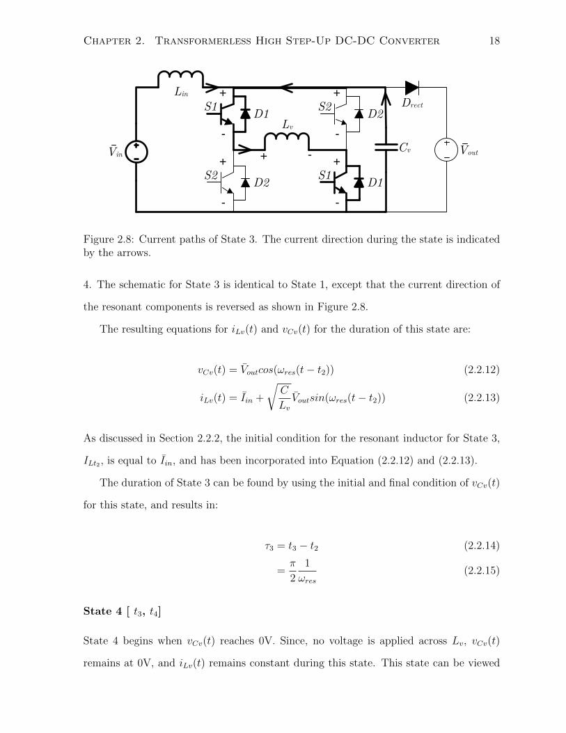
4. The schematic for State 3 is identical to State 1, except that the current direction of
the resonant components is reversed as shown in Figure 2.8.
The resulting equations for iLv(t) and vCv(t) for the duration of this state are:
vCv(t) = Voutcos(ωres(t− t2)) (2.2.12)
iLv(t) = Iin +
√C
LvVoutsin(ωres(t− t2)) (2.2.13)
As discussed in Section 2.2.2, the initial condition for the resonant inductor for State 3,
ILt2 , is equal to Iin, and has been incorporated into Equation (2.2.12) and (2.2.13).
The duration of State 3 can be found by using the initial and final condition of vCv(t)
for this state, and results in:
τ3 = t3 − t2 (2.2.14)
=π
2
1
ωres(2.2.15)
State 4 [ t3, t4]
State 4 begins when vCv(t) reaches 0V. Since, no voltage is applied across Lv, vCv(t)
remains at 0V, and iLv(t) remains constant during this state. This state can be viewed

Chapter 2. Transformerless High Step-Up DC-DC Converter 19
Vin
Lin
Lv
Vout
Drect
Cv
D1
-
S1+
D2
-
S2+
D1
-
S1+
D2
-
S2+
Vin
Lin
Lv
Vout
Drect
Cv
iin
iLv
D1
-
S1+
D2
-
S2+
D1
-
S1+
D2
-
S2+
Vin
Lin
Lv
Vout
Drect
Cv
D1
-
S1+
D2
-
S2+
D1
-
S1+
D2
-
S2+
Vin
Lin
Lv
Vout
Drect
Cv
D1
-
S1+
D2
-
S2+
D1
-
S1+
D2
-
S2+
Vin
Lin
Lv
Vout
Drect
Cv
D1
-
S1+
D2
-
S2+
D1
-
S1+
D2
-
S2+
Vin
Lin
Lv Vout
Drect
Cv
D1
-
S1+
D2
-
S2+
D1
-
S1+
D2
-
S2+ + -
+ -
+ -
+ - + -
+
-
vCv
Figure 2.9: Current paths of States 4. Arrows on the branches indicate current direction.
as a hold state because the state of the resonant components are unchanging. Figure 2.9
depicts the current flow in the circuit during State 4. iLv(t) is shown to flow through all
switches, and the reason is discussed later in Section 4.2.1. Therefore, the state equations
are
vCv(t) = 0 (2.2.16)
iLv(t) = ILt3 (2.2.17)
for the duration of this state. ILt3 is the initial condition of the resonant inductor current
defined in Equation (2.2.18).
ILt3 = Iin +
√CvLvVout (2.2.18)
The duration of State 4, τ4, is left as a variable used to control the power delivered to
the output.
State 5 to State 8
State 5 begins by turning switches S1 “off”, and S2 “on”. This starts the process of
charging Cv with Iin and iLv(t). States 5 to 8 maintain the same order of events as State

Chapter 2. Transformerless High Step-Up DC-DC Converter 20
1 to 4, but iLv(t) conducts through the opposite half of the H-bridge. This causes iLv(t)
to be inverted, as shown in Figure 2.4.
2.2.4 State Equation Verification
State equations were verified with simulation in PSCAD/EMTDC. In this simulation, an
ideal current source was used, and the system parameters that were used are shown in
Table 2.2.
Converter Property ValueLv 500 µHCv 0.025µFfsw 2kHzVout 1kVIin 50A
Table 2.2: Simulated Converter Properties
The analytic expressions were verified by comparing the simulated and calculated
values for the initial conditions and durations of the States 1 to 4. The simulated and
calculated values are presented in Table 2.2. With a simulation time step of 0.01µs, the
analytic equations all match simulation.
Unknown Simulated Calculatedτ1 2.41µs 2.34µsτ2 53.40µs 53.42µsτ3 5.46µs 5.55µsτ4 189.75µs 188.69 µsILt0 -57.06A -57.07AILt1 -56.82A -56.84AILt2 49.98A 50.00AILt3 57.07A 57.07A
Table 2.3: Simulated Converter values for Initial Conditions and State Durations for aswitching frequency of 2kHz

Chapter 2. Transformerless High Step-Up DC-DC Converter 21
2.3 Deadtime Requirement and Soft Switching Char-
acteristics
In the presented analysis, the converter operates the switch S1 with a 50% duty cycle,
and the inverted signal is applied to S2. This allows the switches to maintain a current
path for the resonant inductor current, iLv(t), during the switching period. To ensure a
current path for iLv(t) during the switch transitions from S1 to S2 or S2 to S1, a negative
deadtime is required. A short circuit is avoided because switch transitions occur while
0V is applied across the switches as can be seen in Figure 2.10.
With the negative deadtime, the proposed converter is capable of providing soft
switching opportunities to its switching devices, as identified in Figure 2.10. The ac-
tive switches, S1 and S2, achieve ZVS at their turn “on” and turn “off”. Using S1 as
an example, during State 8, the resonant capacitor voltage, vCv(t), is 0V, and ZVS turn
“on” is guaranteed by the negative deadtime. At the end of State 4, S1 is turned “off”
while vCv(t) is still 0V; this achieves ZVS.
For the rectifying diode, Drect, it has a ZVS turn “off”, but the turn “on” process
is a hard turn “on”. Turn “off” for the rectifying diode occurs at the end of State 2
when iLv(t) has diverted the average input current, Iin, from the rectifying diode and
current is no longer transferred to the output. During State 3, the resonant inductor, Lv,
discharges the resonant capacitor, Cv, causing iLv(t) to increase and vCv(t) to decrease to
0V. The rectifying diode is gradually reverse biased during the transition from State 2 to
State 3, and ZVS is achieved because Lv provides a current path to extract the reverse
recovery charge, Qrr, from the rectifying diode before discharging Cv during State 3.
The rectifying diode is turned “on” at the end of State 1 and beginning of State 2,
and is required to conduct iLv(t) and Iin at turn “on”. The forward recovery of the
diode causes iLv(t) and Iin to continue charging Cv, thus causing overshoot and turn
“on” losses. The overshoot can be minimized with a larger Cv.

Chapter 2. Transformerless High Step-Up DC-DC Converter 22
iLv
vCv
iin
S1
S2
State 1State 2
State 3State 4
Vout
Drect ZVS
S1 ZVS Turn “on”
Drect Turn On
State 8
S1 ZVS Turn “off”
t
t
t
t
State 5
Figure 2.10: Soft switching instances are shown on the waveforms of iLv(t), vCv(t), andiin(t). Gating signals to S1 and S2 are also depicted with negative deadtime.
2.4 Energy Balance
Using the state equations, energy balance can be applied across the input inductor to
relate the output power to the control variable, the switching frequency. Energy balance
results in a solution for the average input current given that the application will specify
the input and output voltage.
2.4.1 Control Variable
As previously mentioned, the switching frequency, fsw, is used as a control variable to
control power delivery to the output. In most converters, increasing this hold state implies
that power delivered to the output is less frequent. However, this converter’s hold states,

Chapter 2. Transformerless High Step-Up DC-DC Converter 23
State 4 and State 8, are used to maintain the volt-sec balance for the input inductor,
Lin. A lower fsw implies a longer State 4 and State 8, which increases the average input
current, Iin, and an increase in the power delivered during the next period. By varying
fsw, the volt-second balance can be adjusted to attain a specific Iin. Therefore, this state
should be referred to as the input inductor charging state instead of a holding state, and
the remainder of this thesis refers to State 4 and 8 as the input inductor charging states.
2.4.2 Energy Balance Calculation
To relate the output power to the control variable, the energy delivered to the output per
period, Eout is derived and equated to the input energy per period, Ein. First solving for
Eout, the only states that deliver energy to the output are State 2 and 6. These are the
rectifying states in a single switching period. Calculating the energy delivered by one of
rectifying states only describes half the energy delivered from a single period. Based on
the circuit diagram of State 2 in Figure 2.6, the energy delivered to the output from a
single rectification state is:
Eout2
=
∫ τ2
0
Vout(Iin − iLv(t))dt (2.4.1)
Substituting Equations (2.2.8), (2.2.9), and (2.2.11) from State 2, Eout becomes
Eout = 4Lv
(I2in + Iin
√CvLvVout
)(2.4.2)
To solve for the input energy per period, the input voltage source, Vin is observed. Since,
Vin is always connected to the input inductor, Lin, then Ein results in
Ein =VinIinfsw
(2.4.3)

Chapter 2. Transformerless High Step-Up DC-DC Converter 24
where fsw is the switching frequency of the converter, and is defined as follows
fsw =1
τsw=
1
2(τ1 + τ2 + τ3 + τ4)(2.4.4)
Since the converter is assumed ideal, Ein can be equated to Eout, and this results in:
Ein = Eout (2.4.5)
Vinfsw
= 4Lv Iin + 2√CvLvVout (2.4.6)
Solving for Iin gives:
Iin =Vin
4Lvfsw−√CvLvVout (2.4.7)
With Equation (2.4.7), Iin, iLv(t), and vCv(t) are determined during a switching period
in steady state.
2.4.3 Verification of Iin
In Section 2.2.4, simulations were performed with an ideal current source. However,
in the actual system, an input inductor, Lin, is used to approximate a current source.
Therefore, the calculated average input current should be verified against the simulated
input current value. The converter components used for the simulations are shown in
Table 2.4, the input inductor and switching frequency are used as variables.
Converter Property ValueLv 500 µHCv 0.025 µHVin 100VVout 1kV
Table 2.4: Simulated Converter Properties

Chapter 2. Transformerless High Step-Up DC-DC Converter 25
It is shown that as the ratio between Lin and resonant inductor, Lv, increases, Lin
better approximates a current source and converges upon the original solution to the
average input current, Iin. Table 2.5 shows a comparison of Iin to the simulated Iin,
as the ratio between Lin and Lv is increased. As expected, the simulated average input
current matches the analytic solution as the ratio LinLv
is increased.
Simulated IinSwitching Frequency Calculated Iin
LinLv
: 10 LinLv
: 100 LinLv
: 1000
4 kHz 5.43A 6.26A 5.52A 5.45A2 kHz 17.92A 19.9A 18.13A 17.96A
Table 2.5: Simulated Verification of Iin with different values of Lin, and fsw
For lower values of LinLv
, the ripple of the input inductor causes an offset in the solution
of the average input current. This situation is presented in Figure 2.11, and shows that
the solution to the average input current would always underestimate the true average
input current.
2.5 Maximum Switching Frequency Limitation
The operation of the proposed converter is limited by a maximum switching frequency,
which occurs when the resonant capacitor voltage, vCv(t), reaches a maximum of Vout in
State 1, and immediately transitions to State 3. To determine the frequency limit, volt
second balance is applied to the input inductor, Lin, over States 1 to 4, and results in
Equation (2.5.1)
∫ τsw2
t0
Vindt =
∫ t1
t0
vCv(t)dt+
∫ t2
t1
vCv(t)dt+
∫ t3
t2
vCv(t)dt+
∫ t4
t3
vCv(t)dt (2.5.1)
As previously mentioned, the converter immediately transfers from State 1 to State 3
when vCv(t) reaches the output voltage, Vout. Thus, State 2 does not exist in the case of

Chapter 2. Transformerless High Step-Up DC-DC Converter 26
iLv
vCv
iin
1 438 2
Vout
State
iin via Energy Balance
Actual iin
t
t
Figure 2.11: Waveforms of iLv(t), vCv(t), and iin(t) with ripple added to iin(t).
the maximum frequency limit, and does not need to be considered in Equation (2.5.1).
In addition, vCv(t) is 0V for the duration of State 4, and its integral equates to 0. Using
these facts, Equation (2.5.1) becomes
∫ τsw2
t0
Vindt =
∫ t1
t0
vCv(t)dt+
∫ t2
t1
vCv(t)dt (2.5.2)
Substituting the state equations for vCv(t) into Equation (2.5.2) would result in
∫ τsw2
t0
Vindt =
∫ t1
t0
(2Iin
√LvCv
+ Vout)sin(ωres(t− t0)dt
+
∫ t3
t2
Voutcos(ωres(t− t2))dt(2.5.3)
During the maximum frequency limit, power is not delivered to the output and the
system is in steady state. Therefore, the average input current, Iin is 0A. This simplifies

Chapter 2. Transformerless High Step-Up DC-DC Converter 27
Equation (2.5.3) to Equation (2.5.4)
∫ τsw2
t0
Vindt =
∫ t1
t0
Voutsin(ωres(t− t0))dt+
∫ t3
t2
Voutcos(ωres(t− t2))dt (2.5.4)
To evaluate the integrals, the end conditions for each state must be revisited. State
1 ends when vCv(t) equals Vout, and State 3 ends when vCv(t) reaches 0V. Using these
facts to evaluate the integral, and solving for the inverse of the switching period results
in
1
τsw= fmax =
VinVout
π
2fres (2.5.5)
where
fres =1
2π√LvCv
(2.5.6)
and fmax is the maximum switching frequency
Verification of fmax was accomplished through simulation with two different ratios of
the input inductor to the resonant inductor, LinLv
. Using the same converter components
as Table 2.4, results of the simulation are presented in Table 2.6.
fmax with fmax with fmax withCurrent Source Lin
Lv= 10 Lin
Lv= 100
7.07 kHz 7.40kHz 7.09kHz
Table 2.6: Simulated Verification of fmax

Chapter 3
Converter Dynamics and Control
This chapter expands upon the analysis of the proposed converter by developing a dy-
namic model. A controller is then developed to regulate input current. Verification
of both the model and controller is accomplished by comparing the analytic model to
PSCAD simulation.
3.1 Converter Dynamics
Resonant converter dynamics cannot be directly obtained with standard state-space av-
eraging methods [19]. The state-space averaging method assumes the following:
1. The switching frequency is much higher than the natural frequency of the converter.
2. All inputs are constant for the duration of the switching period.
Both assumptions do not apply to the proposed converter. The first assumption does
not apply because of the maximum allowable switching frequency, fmax, is below the
resonant frequency of the converter. This is seen from Equation (2.5.5) and is repeated
as Equation (3.1.1) for convenience.
fmax =VinVout
π
2fres (3.1.1)
28

Chapter 3. Converter Dynamics and Control 29
The second assumption is invalid because the resonant component states are inputs to
the system, which are not constant, but vary at the resonant frequency.
Instead, the dynamic model of the current-based resonant converter is obtained by
applying time-averaging to the input inductor and output filter capacitor. This method
assumes the dynamics of the resonant network, Lv and Cv, can be ignored for two reasons.
The first reason is a consequence of assuming the input voltage, output voltage, and input
current are constant for steady state analysis. The filter components required to realize
the assumption are large enough that the energy delivered to the filters in a single period
have negligible effect on their average values. This is a similar assumption to that made
in [20]. The second reason is a result of fmax given by Equation (3.1.1). For high step-
up ratios, Equation (3.1.1) guarantees that the switching frequency is slower than the
resonant frequency of the resonant inductor and capacitor. Thus, the dynamics caused
by the resonant components can be ignored.
The assumptions for the dynamic model are identical to the assumptions used for
steady state analysis with the addition that the internal dynamics can be ignored. These
assumptions are:
1. All components are ideal.
2. The ratio between the input inductor, Lin, and resonant inductor, Lv, should be
much greater than 1, LinLv
>> 1, such that the input inductor can be assumed to be
a constant current source.
3. All sources are constant over a switching period.
4. Energy balance is maintained between the input and output of the converter.
5. Internal dynamics of the resonant tank are much faster than the switching period
and can be ignored or, equivalently, the energy stored in the tank elements is much
smaller than that stored in the input inductor, Lin.

Chapter 3. Converter Dynamics and Control 30
The dynamics included in the model are the input inductor, Lin, and output capacitor
Cout. The dynamic equation for the input inductor is derived by averaging the voltage
applied across it over one switching period, τsw. Similarly, the dynamic equation for the
output capacitor is produced by averaging the current flow into the output capacitor over
a switching period.
Referring to Figure 2.4, time averaging is applied across the input inductor would
result in the dynamic equation for Lin, Equation (3.1.2).
Lind〈iin(t)〉τsw
dt= 〈vin(t)〉τsw − 〈vCv(t)〉τsw (3.1.2)
where the following notation is employed
〈x(t)〉τsw =1
τsw
∫ τsw
0
x(t)dt (3.1.3)
Assuming that the input sources are constant over a switching period implies that the
dynamic waveforms for the resonant capacitor and inductor do not differ much from
the steady state waveforms. Thus, the steady state equations for the resonant capacitor
voltage developed in Chapter 2 can be used to express the averaged resonant capacitor
voltage in terms of system quantities and state variables, and results in Equation (3.1.4)
Lind〈iin(t)〉τsw
dt= 〈vin(t)〉τsw − 4Lvfsw
[〈iin(t)〉τsw +
√CvLv〈vout(t)〉τsw
](3.1.4)
Averaging the current into the output capacitor can be described as
Coutd〈vout(t)〉τsw
dt=
Pout〈vout(t)〉τsw
− 〈vout(t)〉τswRLoad
(3.1.5)
where Pout is the energy delivered to the output over a switching period. Pout is found by
using Equation (2.4.2), which is the energy delivered to the output over half a switching

Chapter 3. Converter Dynamics and Control 31
period, Eout. The output power delivered during a switching period would be
Pout = fswEout (3.1.6)
Substituting Eout into Pout and using that result in the dynamic equation of the output
capacitor produces
Coutd〈vout(t)〉τsw
dt=
4Lvfsw〈vout(t)〉τsw
(〈iin(t)〉2τsw +
√CvLv〈vout(t)〉τsw〈iin(t)〉τsw
)
− 〈vout(t)〉τswRLoad
(3.1.7)
It should be noted that the dynamic equation assumes an ideal current source. How-
ever, as discussed in Section 2.4.3, when an input inductor is used instead of an ideal
current source, the solution for the average input current is offset due to the input cur-
rent ripple. Thus, it is expected that the dynamic equations would produce an input
current lower than that of the simulated converter. The predicted output voltage from
the analytic equations would also be lower due to the lower input current.
To verify the accuracy of the dynamic equations, a step-response was performed with
the analytic model, and compared to the PSCAD simulation. A step in the input voltage,
vin(t), and the switching frequency, fsw, was provided to the dynamic equations, which
are the input variables of Equation (3.1.4) and (3.1.7). Both step responses start with
an input voltage of 100V and a switching frequency of 4kHz.
The step response for the input voltage provides a step input from 100V to 200V,
and a separate step response changes the switching frequency from 4kHz to 1kHz. The
converter properties for simulation are listed in Table 3.1 and the step responses are
shown in Figure 3.1 to 3.4

Chapter 3. Converter Dynamics and Control 32
Converter Property ValueCout 500µFLin 5 mHLv 500 µHCv 0.025µFRLoad 1800Ω
Table 3.1: Simulated Converter Properties
Both step responses show the analytic model and PSCAD simulations are similar, but
the analytic model is offset from the averaged value of the PSCAD simulation. Similar to
the steady state analysis, the analytic model under estimates the value of both the input
current and output voltage. For comparison, Figure 3.5 and 3.6 use a input inductor to
resonant inductor ratio, LinLv
, of 100 instead of 10 to better approximate an ideal current
source. The figures show the simulation and analytic model converging and implies that
the dynamic equations can be used for control.

Chapter 3. Converter Dynamics and Control 33
Figure 3.1: Step Response of iin(t) due to a step in switching frequency from 4kHz to1kHz
Figure 3.2: Step Response of vout(t) due to a step in switching frequency from 4kHz to1kHz

Chapter 3. Converter Dynamics and Control 34
Figure 3.3: Step Response of iin(t) due to a step in vin(t) from 100V to 200V
Figure 3.4: Step Response of vout(t) due to a step in vin(t) from 100V to 200V

Chapter 3. Converter Dynamics and Control 35
Figure 3.5: Step Response of iin(t) due to a step in switching frequency from 4kHz to1kHz with Lin of 50mH
Figure 3.6: Step Response of vout(t) due to a step in switching frequency from 4kHz to1kHz with Lin of 50mH

Chapter 3. Converter Dynamics and Control 36
3.2 Current Compensator
This section develops a method of control for the input current while the input and output
voltage are assumed constant. The purpose of this section is to determine a method to
manage the nonlinear aspects of the dynamic equations.
The first option is to apply perturbation and linearization to the plant. The input
current and switching frequency are perturbed while the input and output voltage are
held constant. Small signal AC quantities of the perturbation are represented by x.
Lind
dt(Iin + iin) = Vin − 4Lv(fsw + fsw)
[(Iin + iin) +
√CvLvVout
](3.2.1)
Separating the DC and AC terms of Equation (3.2.1) would result in the following
equations
Lind
dtIin = 0 = Vin − 4Lvfsw
[Iin +
√CvLvVout
](3.2.2)
Lind
dtiin = 4Lv(fsw iin + fswIin + fsw iin)− 4Lv
√CvLv
¯Voutfsw (3.2.3)
From Equation (3.2.3), a small signal plant can be found by linearizing and rearranging
terms to solve the small signal input current in terms of the small signal switching
frequency. The resulting plant equation is
iin = Gp1
sωp
+ 1fsw (3.2.4)
with coefficients of
Gp = − Vin4Lvf 2
sw
(3.2.5)
ωp = 4LvLbfsw (3.2.6)

Chapter 3. Converter Dynamics and Control 37
The operating point can be substituted into the plant to highlight the dependence on
the state variable iin(t). This resulting equation for Gp is
Gp =
(Iin +
√CvLv
)24Lv
Vin(3.2.7)
The gain, Gp, is shown to be dependent upon the linearized operating point. The plant
may be compensated assuming the highest possible value of Gp. However, in this case
the system would display excessively slow dynamics over a large portion of the operating
range. This is not acceptable because the response of the compensated converter should
be independent of its operating point.
Another approach is used to mitigate the nonlinear aspect of the dynamic equation,
(3.1.4). In Equation (3.1.4), the switching frequency, which is the control variable, is
multiplied by the state, the input current. To mitigate the nonlinearity, an input variable
u is created, and is defined as
u = 4Lvfsw
[〈iin(t)〉τsw +
√CvLvVout
](3.2.8)
The resulting dynamic equation becomes
Lind〈iin(t)〉τsw
dt= Vin − u (3.2.9)
By transforming the system into the Laplace domain, the plant becomes
Iin(s) =1
Lins[Vin − u] (3.2.10)
In Equation (3.2.10), the modified system is simply an integrator with the input voltage
as a disturbance.
The complete control model is shown in Figure 3.7. The output of the system is
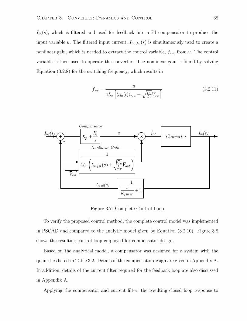
Chapter 3. Converter Dynamics and Control 38
Iin(s), which is filtered and used for feedback into a PI compensator to produce the
input variable u. The filtered input current, Iin fil(s) is simultaneously used to create a
nonlinear gain, which is needed to extract the control variable, fsw, from u. The control
variable is then used to operate the converter. The nonlinear gain is found by solving
Equation (3.2.8) for the switching frequency, which results in
fsw =u
4Lv
[〈iin(t)〉τsw +
√CvLvVout
] (3.2.11)
𝐾𝑝 +𝐾𝑖𝑠
1
𝐿𝑖𝑛𝑠
Vin
1𝑠
𝜔𝑓𝑖𝑙𝑡𝑒𝑟+ 1
uIref
-
-
Converter𝐾𝑝 +𝐾𝑖𝑠
1𝑠
𝜔𝑓𝑖𝑙𝑡𝑒𝑟+ 1
Iin fil(s)
Iref(s)
-
Iin(s)X
1
4𝐿𝑣 𝐼𝑖𝑛 𝑓𝑖𝑙 (𝑠) + 𝐶𝑣𝐿𝑣
𝑉𝑜𝑢𝑡
Vout
u fsw
Compensator
Nonlinear Gain
Figure 3.7: Complete Control Loop
To verify the proposed control method, the complete control model was implemented
in PSCAD and compared to the analytic model given by Equation (3.2.10). Figure 3.8
shows the resulting control loop employed for compensator design.
Based on the analytical model, a compensator was designed for a system with the
quantities listed in Table 3.2. Details of the compensator design are given in Appendix A.
In addition, details of the current filter required for the feedback loop are also discussed
in Appendix A.
Applying the compensator and current filter, the resulting closed loop response to

Chapter 3. Converter Dynamics and Control 39
𝐾𝑝 +𝐾𝑖𝑠
1
𝐿𝑖𝑛𝑠
Vin
1𝑠
𝜔𝑓𝑖𝑙𝑡𝑒𝑟+ 1
uIref
-
-
Converter𝐾𝑝 +𝐾𝑖𝑠
1𝑠
𝜔𝑓𝑖𝑙𝑡𝑒𝑟+ 1
Iin fil(s)
Iref(s)
-
Iin(s)X
1
4𝐿𝑣 𝐼𝑖𝑛 𝑓𝑖𝑙 (𝑠) + 𝐶𝑣𝐿𝑣
𝑉𝑜𝑢𝑡
Vout
u fsw
Compensator
Nonlinear Gain
Figure 3.8: Analytic Model
Converter Property ValueLin 5mHLv 500 µHCv 0.025 µHVin 100VVout 1kV
Table 3.2: Converter Properties for Current Compensator Simulation
disturbances and a step in the input current reference is shown in Figure 3.9 to Figure
3.11. All three responses show good matching between the analytic model and simulation.
The unfiltered response of the input current for both the analytic model and simulation
are plotted against each other for all three figures. Figure 3.9 shows a step response
of the input current set point from 10A to 50A. Figure 3.10 shows the response of the
system due to a disturbance of the input voltage, which was changed from 100V to 110V.
The last figure, Figure 3.11, shows the response of the system due to a disturbance on
the output voltage for a change of 1kV to 1.1kV. The analytic model does not contain
a dependence on the output voltage, and simulation shows that the output voltage does
have little effect on the input current.

Chapter 3. Converter Dynamics and Control 40
Figure 3.9: Simulation response comparing iin(t) of the Analytic model and PSCADsimulations when a step in reference input current from 10A to 50A is applied.
Figure 3.10: Simulation response comparing iin(t) of the Analytic model and PSCADsimulations when a step in input voltage from 100V to 110V is applied.

Chapter 3. Converter Dynamics and Control 41
Figure 3.11: Simulation response comparing iin(t) of the Analytic model and PSCADsimulations when a step in output voltage from 1kV to 1.1kV is applied.

Chapter 4
Converter Design
This chapter develops the component ratings, theoretical efficiency, and design procedure
by using the state equations developed in Chapter 2. However, a refinement to the aver-
age input inductor current is first introduced to improve the accuracy of the component
ratings and theoretical efficiency. These topics are discussed in five sections. The first
section introduces a refinement to the solution of the average input inductor current. The
second section examines the waveforms of the switches, and develops switch character-
istics and requirements. The third section develops the passive component ratings. The
fourth section uses the information from the previous sections to estimate the efficiency
of the converter, and the final section details the design methodology for choosing each
component.
4.1 Refinement in Iin
In the analysis from Chapter 2, the input inductor was assumed large enough to mimic
a constant current source, as such the ripple of the input current has been omitted from
analysis. This results in an offset in the estimated average value of the input current.
Once again using Figure 2.11, and repeating it as Figure 4.1, it is shown how the original
average input current found through energy balance would differ from the actual input
42

Chapter 4. Converter Design 43
current. For reference, the original equation for the average input current, Equation
(2.4.7), is repeated as Equation (4.1.1)
Iin =Vin
4Lvfsw−√CvLvVout (4.1.1)
iLv
vCv
iin
1 438 2
Vout
State
iin via Energy Balance
Actual iin
t
t
Figure 4.1: Waveforms of iLv(t), vCv(t), and iin(t) with ripple added to iin(t).
By inspecting Figure 4.1, a refinement to the estimated average input current can be
made by utilizing the ripple of the input current. The original averaged input current,
Iin, was solved by assuming the input current, iin(t) and resonant inductor current,
iLv(t), intersected at Iin. Instead, it can be assumed that energy balance solved for the
resonant inductor’s initial current at State 3 instead of Iin, as depicted in Figure 4.1, and
the initial current at State 3 is assumed to be offset from the average input current by
half the peak to peak input current. From these assumptions, Equation (4.1.1) becomes
Equation (4.1.2).

Chapter 4. Converter Design 44
Iin −1
2∆iinpk−pk =
Vin4Lvfsw
−√CvLvVout (4.1.2)
Before solving for the refined average input current, an assumption was made about
the input current ripple. Since voltage balance across the input inductor, Lin depends on
the resonant capacitor voltage, vCv(t) and input voltage, Vin. A simple approximation of
the ripple is to only use the states with constant voltage applied across Lin to estimate
the ripple.
This approximation is justified because the switching module’s purpose is to aid in the
turn “on” and turn “off” process of the rectifying diode, Drect. State 2 is the rectifying
state where energy is transferred to the output, and State 4 is the input inductor charging
state required to maintain volt-sec balance across Lin. State 1 and State 3 can be viewed
as transition states where the module aids in turning Drect “on” and “off”, and can be
assumed to be short in duration. Thus, the ripple can be calculated through State 2
or State 4. State 2 is chosen to calculate the ripple because the duration of State 4 is
dependent on the duration of States 1 to 3. Therefore, using State 4 would not yield a
simpler expression for the input current ripple.
The peak to peak input ripple current can be approximated by
∆iinpk−pk ≈Vin − Vout
Linτ2 (4.1.3)
Using Equation (2.2.11) to replace τ2 results in the full expression as follows
∆iinpk−pk ≈ 2LvLin
(VinVout− 1
)√I2in + Iin
√CvLvVout (4.1.4)

Chapter 4. Converter Design 45
By substituting Equation (4.1.4) into Equation(4.1.2) results in
Iin −LvLin
(VinVout− 1
)√I2in + Iin
√CvLvVout =
Vin4Lvfsw
−√CvLvVout (4.1.5)
Rearranging the terms into quadratic form.
aI2in + bIin + c = 0 (4.1.6)
where
a =
[1−
((VinVout− 1)
LvLin
)2]
(4.1.7)
b = −
[2
(Vin
4Lvfsw−√CvLvVout
)+
((VinVout− 1
)LvLin
)2√CvLvVout
](4.1.8)
c =
(Vin
4Lvfsw−√CvLvVout
)2
(4.1.9)
The final solution for the refined Iin is the larger solution of the quadratic equation. The
refinement to Iin is based on the assumption that State 2 is much longer than States
1 and 3. Since State 2 is also the rectifying state then the refined Iin should only be
considered valid near maximum power transfer to maintain this assumption.
4.1.1 Verification of the Refinement to Iin
The original Iin and the refined Iin are verified against the simulated input current. The
converter components used for the simulations are shown in Table 4.1. Figure 4.2 plots
the original and refined Iin against the simulated values, and Table 4.2 shows the error
between the calculated Iin and simulated.
The refined version of Iin is not exact due to the omission of State 1 and 3, but is a bet-
ter approximation to the simulated values than the original solution for Iin. The original

Chapter 4. Converter Design 46
Converter Property ValueLin 5mHLv 500 µHCv 0.025 µHVin 100VVout 1kV
Table 4.1: Simulated Converter Properties
Figure 4.2: Comparison of original and refined average input current to the simulatedaverage input current.
solution yields simpler equations and provides more insight into the relationship between
converter components and operating specifications while the refined version should be
used in calculating component ratings.

Chapter 4. Converter Design 47
Error in % Error in %of Rated Iin
Switching Original Refined Original RefinedFrequency Iin (%) Iin (%) Iin (%) Iin (%)
7 kHz 82.93 58.54 1.71 1.216 kHz 24.42 6.98 2.11 0.605 kHz 17.00 1.42 3.02 0.254 kHz 13.26 0.16 4.17 0.053 kHz 11.11 0.46 6.03 0.252 kHz 9.95 0.60 9.95 0.60
Table 4.2: Simulated Verification of the refined version of Iin. Rated Iin is 19.9A
4.2 Switch Requirements and Ratings
This section specifies the switch ratings required by the switches in the proposed con-
verter. The following discussion on switch requirements and ratings is heavily dependent
on State 4 and 8, and the current that conducts through the resonant inductor during
these states. The circuit diagram of State 4, and the resonant inductor current equa-
tion during State 4 are repeated here for convenience, as they will be referred to in the
following sub-sections.
Vin
Lin
Lv
Vout
Drect
Cv
D1
-
S1+
D2
-
S2+
D1
-
S1+
D2
-
S2+
Vin
Lin
Lv
Vout
Drect
Cv
iin
iLv
D1
-
S1+
D2
-
S2+
D1
-
S1+
D2
-
S2+
Vin
Lin
Lv
Vout
Drect
Cv
D1
-
S1+
D2
-
S2+
D1
-
S1+
D2
-
S2+
Vin
Lin
Lv
Vout
Drect
Cv
D1
-
S1+
D2
-
S2+
D1
-
S1+
D2
-
S2+
Vin
Lin
Lv
Vout
Drect
Cv
D1
-
S1+
D2
-
S2+
D1
-
S1+
D2
-
S2+
Vin
Lin
Lv Vout
Drect
Cv
D1
-
S1+
D2
-
S2+
D1
-
S1+
D2
-
S2+ + -
+ -
+ -
+ - + -
+
-
vCv
Figure 4.3: Current paths of States 4. Arrows on the branches indicate current direction.
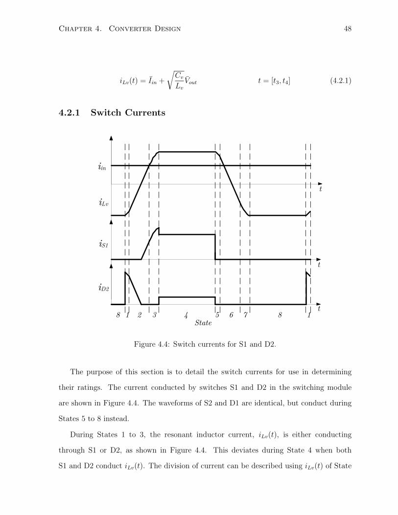
Chapter 4. Converter Design 48
iLv(t) = Iin +
√CvLvVout t = [t3, t4] (4.2.1)
4.2.1 Switch Currents
iLv
iin
1 438 2State
iD2
iS1
5 6 7 8 1t
t
t
Figure 4.4: Switch currents for S1 and D2.
The purpose of this section is to detail the switch currents for use in determining
their ratings. The current conducted by switches S1 and D2 in the switching module
are shown in Figure 4.4. The waveforms of S2 and D1 are identical, but conduct during
States 5 to 8 instead.
During States 1 to 3, the resonant inductor current, iLv(t), is either conducting
through S1 or D2, as shown in Figure 4.4. This deviates during State 4 when both
S1 and D2 conduct iLv(t). The division of current can be described using iLv(t) of State

Chapter 4. Converter Design 49
4, Equation (4.2.1), and Figure 4.3.
State 4 is the input inductor charging period. The resonant capacitor voltage, vCv(t),
is 0V for the duration of the state, and iLv(t) is constant. iLv(t) during this state,
Equation (4.2.1), can be decoupled into two components. The average input current,
Iin, and a second component. The second component is the current required to charge
the resonant capacitor, Cv, from 0V to Vout. This current is referred to as the resonant
current, Ires, and is defined as:
Ires =
√CvLvVout (4.2.2)
By using Figure 4.3 the paths of the different currents can be highlighted. Iin must
conduct through switch S1 and the resonant inductor, Lv. However, Lv must also conduct
Ires. Since the switches are assumed ideal, Ires flows through the high-side S1 and D2
and low-side S1 and D2 equally. Therefore, the current flowing through S1 in State 4 is
IS1 = Iin +1
2
√CvLvVout t = [t3, t4] (4.2.3)
and the current in D2 during State 4 is
ID2 =1
2
√CvLvVout t = [t3, t4] (4.2.4)
4.2.2 Switch Ratings
This section develops the voltage and current ratings of all the switches in this converter.
The current ratings for switches S1, and S2 can be defined with Figure 4.4. The peak
switch current occurs at the end of State 3 and is equal in magnitude to Equation (4.2.1).
The RMS current could be directly integrated, but an approximation can be made in
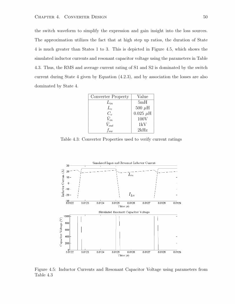
Chapter 4. Converter Design 50
the switch waveform to simplify the expression and gain insight into the loss sources.
The approximation utilizes the fact that at high step up ratios, the duration of State
4 is much greater than States 1 to 3. This is depicted in Figure 4.5, which shows the
simulated inductor currents and resonant capacitor voltage using the parameters in Table
4.3. Thus, the RMS and average current rating of S1 and S2 is dominated by the switch
current during State 4 given by Equation (4.2.3), and by association the losses are also
dominated by State 4.
Converter Property ValueLin 5mHLv 500 µHCv 0.025 µHVin 100VVout 1kVfsw 2kHz
Table 4.3: Converter Properties used to verify current ratings
Figure 4.5: Inductor Currents and Resonant Capacitor Voltage using parameters fromTable 4.3

Chapter 4. Converter Design 51
Utilizing the approximation, it is assumed that S1 and S2 each conduct the current
given by Equation (4.2.3) for half the duration of the switching period. The resulting
RMS current rating for S1 and S2 is
IswRMS =1√2
(Iin +
√CvLv
Vout2
)(4.2.5)
As a consequence, the average current is
IswAV G =1
2
(Iin +
√CvLv
Vout2
)(4.2.6)
The average and RMS current of D1 and D2 is also dominated by the current conducted
during State 4. This results in
IswdRMS =1√2
(√CvLv
Vout2
)(4.2.7)
IswdAV G =1
2
(√CvLv
Vout2
)(4.2.8)
The switch rating of the rectifying diode, Drect, depends upon State 2 and 5. From
Figure 4.6, which is a repeat of Figure 2.6, the peak and average current can be inferred.
The peak current is the combination of Iin and iLv(t) at the beginning of State 2 or 5, and
is given in Equation (4.2.9). The diode current decreases linearly over the rectifying state,
and a direct integration results in the average and RMS current presented in Equation
(4.2.10), and Equation (4.2.11) respectively.

Chapter 4. Converter Design 52
iLv
vCv
iin
1 438t
2State
iLv
vCv
iin
1 438
t
2State
iDrect
𝜏1 𝜏2 𝜏3 𝜏4
Vout
t
Figure 4.6: The rectifying current, iDrect(t), and the currents that it is composed of iLv(t)and Iin
Idpeak = 2
√I2in + Iin
√CvLvVout (4.2.9)
Idavg = 4fLvVout
(I2in + Iin
√CvLvVout
)(4.2.10)
Idrms =
√√√√16
3fsw
LvVout
(I2in + Iin
√CvLvVout
)(4.2.11)
The voltage rating of Drect, S1, S2, D1, and D2 all depend on the resonant capacitor
voltage, vCv(t). From Figure 4.6, it can be seen that vCv(t) varies from 0V to Vout, thus
all switches must be rated for Vout. Since the peak rectifying current is approximately
twice that of the average input current, overshoot should be expected. Thus, a safety
margin of 50% of Vout is used.

Chapter 4. Converter Design 53
The switch ratings were verified with simulation and the results of comparison can
be found in Table 4.4. The values were calculated using components listed in Table 4.3.
Since all quantities are in terms of Iin, the original and refined versions of Iin were used
for comparison. Due to the approximation that State 4 and State 8 dominate the current
rating of the switches, the ratings which use the refined Iin tend to over estimate the
simulated values, but still shows closer agreement to the simulated values.
Switch RatingSwitch Original Iin Refined Iin SimulatedS1/S2 15.18 Arms 16.64 Arms 15.2 Arms
10.37Aavg 10.74Aavg 11.77AavgD1/D2 2.5Arms 2.5Arms 2.92Arms
1.77 Aavg 1.77Aavg 1.45AavgDrect 42.34 Apk 46.54 Apk 45.56 Apk
1.79Aavg 2.17 Aavg 1.96 Aavg7.10Arms 8.20Arms 7.78 Arms
Table 4.4: Verification of Switch Ratings
4.3 Passive Component Ratings
This section will discuss the ratings for the input inductor, resonant inductor and reso-
nant capacitor. Similar to the switch voltage ratings, the voltage rating of the resonant
inductor is dependent on the resonant capacitor voltage, vCv(t), thus both the resonant in-
ductor and capacitor should be rated at Vout with the same safety margin as the switches.
The voltage rating for the input inductor is dependent on the difference between Vin and
vCv(t). Therefore the voltage rating of the input inductor is equal to Vout - Vin with a
safety margin.
The current ratings for the passive components can be explained with the aid of
Figure 4.7. For the input inductor, Iin is defined by system requirements. However, the
ripple component of the input current, ∆iinpk−pk , has previously been discussed in the
refinement of Iin and is given in Equation (4.1.4).

Chapter 4. Converter Design 54
iLv
iin
1 438 2State
iCv
5 6 7 8 1
t
t
iLv
iin
1 438 2State
iCv
5 6 7 8 1
t
t
Figure 4.7: Current waveforms for all passive components.
For the resonant inductor, Lv, the peak current is the current that conducts through
Lv during the input inductor charging states, States 4 and 8, and is given by Equation
(4.2.1). In addition, it is assumed that the current ratings are dominated by State 4 and
State 8 for the same reasons used in determining the switch ratings. As a result, the
RMS and average current of Lv is equal to the peak current.
The current requirements of the resonant capacitor, Cv, are determined by State 1 and
3. These are the only two states that charge is delivered or removed from the capacitor
as depicted in Figure 4.7. In State 1, iLv(t) and Iin are directed into Cv, and both are
at their peak values. Therefore, the peak current for the capacitor is at the beginning of
State 1, and is shown in Equation (4.3.2). There are no simplifying methods to determine
the RMS current of the capacitor, and the RMS current is computed and presented in
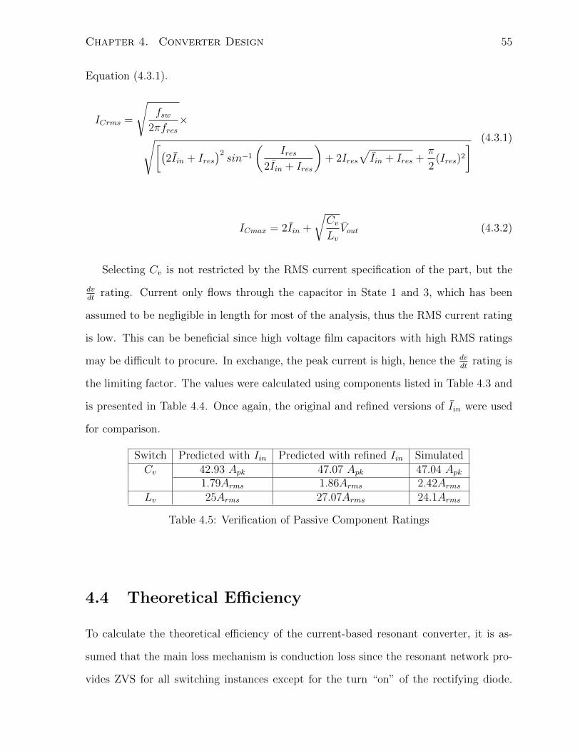
Chapter 4. Converter Design 55
Equation (4.3.1).
ICrms =
√fsw
2πfres×√[(
2Iin + Ires)2sin−1
(Ires
2Iin + Ires
)+ 2Ires
√Iin + Ires +
π
2(Ires)2
] (4.3.1)
ICmax = 2Iin +
√CvLvVout (4.3.2)
Selecting Cv is not restricted by the RMS current specification of the part, but the
dvdt
rating. Current only flows through the capacitor in State 1 and 3, which has been
assumed to be negligible in length for most of the analysis, thus the RMS current rating
is low. This can be beneficial since high voltage film capacitors with high RMS ratings
may be difficult to procure. In exchange, the peak current is high, hence the dvdt
rating is
the limiting factor. The values were calculated using components listed in Table 4.3 and
is presented in Table 4.4. Once again, the original and refined versions of Iin were used
for comparison.
Switch Predicted with Iin Predicted with refined Iin SimulatedCv 42.93 Apk 47.07 Apk 47.04 Apk
1.79Arms 1.86Arms 2.42ArmsLv 25Arms 27.07Arms 24.1Arms
Table 4.5: Verification of Passive Component Ratings
4.4 Theoretical Efficiency
To calculate the theoretical efficiency of the current-based resonant converter, it is as-
sumed that the main loss mechanism is conduction loss since the resonant network pro-
vides ZVS for all switching instances except for the turn “on” of the rectifying diode.

Chapter 4. Converter Design 56
Core loss is also assumed to be negligible. Before dividing the losses into the different
components, the output power is derived. From energy balance, it is known that the
energy delivered to the output over a switching period, Eout, is given in Equation (2.4.2).
Dividing Eout by the switching period results in Pout as follows
Pout = 4Lvfsw
(I2in + Iin
√CvLvVout
)(4.4.1)
For the efficiency calculation, the following conduction losses are included:
1. Resonant Inductor and Input Inductor Winding Resistance
2. Equivalent series resistance (ESR) of the resonant capacitor
3. Switch conduction losses
IGBTs are used as the active switch, and “on” state conduction is modelled by a
constant voltage drop with a resistance in series. The “on” state of the rectifying diode,
and free-wheeling diodes of the IGBTs are modelled in the same manner as a constant
voltage drop with series resistor. The losses of the converter can be summarized as follows
PIGBTLoss = 2VdropIGBT (IswAV G) + 2RonIGBT (IswRMS)2 (4.4.2)
PIGBTDiodeLoss = 2VdropIGBTdiodeIswdAV G + 2RonIGBTdiode(IswdRMS)2 (4.4.3)
PDrectLoss = VdropDrectIdavg +RonDrectIdrms (4.4.4)
Pcomponentloss = RLvI2Lrms +RLinI
2in +RCesri
2Crms (4.4.5)
Of the listed losses, it is expected that the IGBT, and inductor losses will dominate, and
that the ESR of Cv will have negligible effect.

Chapter 4. Converter Design 57
4.5 Design Considerations and Component Sizing
For the proposed converter, three components require sizing, the input inductor, reso-
nant inductor, and resonant capacitor. The sizing of the resonant inductor, Lv and the
resonant capacitor, Cv, should be used to minimize conduction losses by reducing the
currents during the input inductor charging state (State 4 and 8).
During State 4 and 8, the resonant inductor current is constant, and conducts a
current of magnitude equal to Equation (4.2.1), which is composed of the average input
current, Iin, and the resonant current, Ires. The input current cannot be changed, but
Ires can be minimized by reducing the resonant capacitor, Cv, and increasing the resonant
inductor, Lv. Minimizing Ires only constrains the ratio between Cv and Lv.
A constraint can be placed on Lv by examining Iin. From Equation (4.1.1), the size of
Lv directly affects the switching frequency, fsw, assuming Vin and Vout are predetermined.
Therefore, the size of Lv can either limit Ires, or be used to determine the full load
switching frequency.
Several considerations must also be taken into account when choosing the resonant
inductor and capacitor. For the resonant capacitor, Cv, the dvdt
rating will be the limiting
factor for Cv as opposed to the RMS current rating, as discussed in Section 4.3. Although
Lv conducts a constant current during the longest states, State 4 and 8, the transition
states contain high frequencies components. This can be seen in Figure 4.5, thus the
inductor must still be a high frequency inductor to minimize losses.
The size of the input inductor, Lin, is determined by the ripple requirement of iin(t).
The motivation for the sizing is from Equation (4.1.4) where the ripple component of
iin(t) is shown to be proportional to the ratio of Lv to Lin. However, Lin must be
large enough to maintain the constant current source assumption of iin(t). Thus, Lin is
restricted to be at least 10x larger than Lv.
Finding the optimal component size is outside the scope of this thesis, but several
relationships are developed in this discussion. To summarize the relations,

Chapter 4. Converter Design 58
1. The ratio of the resonant inductor, Lv, to the input inductor, Lin, is used to satisfy
input ripple constraint and maintain the constant input current assumption.
2. The ratio of the resonant capacitor to the resonant inductor is used to minimize
conduction loss by reducing the resonant inductor current during State 4 and State
8.
3. The size of Lv is used to either set the frequency of operation or to minimize the
resonant inductor current, Ires.
4. No minimum size restriction exists for the resonant capacitor, Cv. However, it
should be larger than the parasitic capacitance of the switching module.

Chapter 5
Experimental Results
Figure 5.1: Experimental Lab Setup
A prototype of the current-based resonant converter was designed and implemented
to validate the analysis and investigate the losses. This chapter provides details of the
experiment system and results. The first chapter section details the components used
for the converter, and the experimental equipment. The second section discusses an
improvement made to the switching scheme of the converter. The third section covers
experimental results, which includes verifying waveforms and presenting efficiency results.
Improvement to the converter are also suggested and validated in the results section.
59

Chapter 5. Experimental Results 60
The chapter concludes with a summary and comparison of the current-based resonant
converter to the boost converter and voltage-based resonant converter.
5.1 Experiment Setup
A 4kW prototype of the current-based resonant converter was developed and operated
based on open loop control of the converter switching frequency. A circuit diagram of
the experimental setup is given in Figure 5.2, and operating ranges are given in Table
5.1. The prototype’s operation was tested at multiple input voltages with a fixed output
voltage of 1kV. The input voltage for the converter was provided by a DC generator
when Vin was below 130V. For voltages above 130V, the filtered output of a 3-phase
rectifier was used. The rectifier was fed by a transformer connected to the AC grid. Both
input and output voltages were supported by a capacitor bank, both sized at 4.8mF. As
a safety precaution, the output capacitor was over-sized to ensure that a dump of energy
from the inductor at full load would only cause the output voltage to rise by 100V.
Efficiency measurements were performed with four Tektronix TX1 high precision mul-
timeters. Input voltage and output current were measured directly with the multimeters,
while the multimeters measured the input current through a shunt resistor, and the out-
put voltage through a calibrated resistor divider.
Converter Specifications ValueVin 100 - 200 VVout 1 kVfsw 12 - 1 kHz
Poutrated 4 kW
Table 5.1: Experimental Specifications

Chapter 5. Experimental Results 61
Current-Based Resonant Converter
Vin
Lin
Lv
Drect
Cv
D1
-
S1+
D2
-
S2+
D1
-
S1+
D2
-
S2+
Cin
Cout
RLoad
100A Fuse
100ACircuit Breaker
Rsense
M
M
M Multimeter
M
500V
50mV
10A
RDiv1
RDiv2 M
500V
MCUComputer
Gating SignalsIsolated RS232
Vout
+
-
Figure 5.2: Schematic for Experimental Setup
5.1.1 Prototype Parameters
The components chosen for this prototype can be found in Tables 5.2 and 5.3. The tables
detail the passive components and switching components respectively, and includes their
loss mechanics. The loss mechanics were either measured or found from the datasheets.
The rectifying diode, Drect, only specified a forward voltage drop, and no series resistance
value could be extrapolated from the datasheet. RLin also includes the wiring and contact
Converter Component Value PropertiesLv 500 µH RLv = 13.37mΩ, Imax = 182ACv 0.025 µF RCesr = 37.6mΩ, C di
dt= 160A
Lin 5mH RLin = 18.6mΩ, Imax = 75A
Table 5.2: Experimental Component Values
resistance from the input inductor to Drect.
5.2 Switching Scheme
During preliminary operation of the converter, an oscillation in the resonant capacitor
voltage during zero voltage States 4 and 8 was encountered, as shown in Figure 5.3.

Chapter 5. Experimental Results 62
Switch Manufacturer Voltage Current PropertiesNumber Rating Rating
Drect DSDI 60-16A 1600V 63Aavg VFtyp = 2.6VS1 / S2 FS100R17KE3 1700V 100Aavg VFtyp = 0.94V, Rsw = 15mΩD1 / D2 FS100R17KE3 1700V 100Aavg VFtyp = 1.1V, Rsw = 11.6mΩ
Table 5.3: Switching Components used in Experiment
This phenomenon occurred while a switching scheme with a 50% duty cycle and negative
deadtime was utilized, as detailed in Section 2.3.
The resonant inductor current, iLv(t) and input inductor current, iin(t), in State 4 are
analyzed to understand the reason for the oscillations. Figure 5.5 depicts the currents
in this situation. During States 4, iLv(t), is circulating through the switches and slowly
dissipating. Meanwhile, iin(t), is increasing at a constant rate, storing energy for the next
period. At higher power, State 4 increase in duration, and the two currents eventually
coincide. When this occurs, D2 turns “off” and the reverse recovery charge of D2 creates
the oscillations as shown in Figure 5.3.
The oscillations can be removed by activating all four IGBTS during State 4, lead-
ing to alternative switching signals shown in Figure 5.6. The result of the alternative
switching signals on converter operation is shown in Figure 5.4. With the alternative
switching scheme, when iin(t) exceeds iLv(t), the difference between iin(t) and iLv(t) has
an alternative conduction path through S2, and D2 has a source to provide the reverse
recovery charge. The alternative PWM scheme also leads to an improvement in converter
efficiency. Figure 5.7 compares efficiency curves of the two different switching schemes.
5.3 Experiment Results
This section examines the measured waveforms and compares them to the expected
waveforms used in analysis. Efficiency curves are presented in this section, but show a
discrepancy between theoretical and experimental curves. This difference is examined

Chapter 5. Experimental Results 63
Figure 5.3: Waveforms of iLv(t), vCv(t), and iin(t) with Regular PWM Scheme. vCv(t) isshown in Ch1. iin(t) is shown in Ch3. iLv(t) is shown in Ch4.
Figure 5.4: Waveforms of iLv(t), vCv(t), and iin(t) with Alternate PWM Scheme. vCv(t)is shown in Ch1. iin(t) is shown in Ch3. iLv(t) is shown in Ch4.

Chapter 5. Experimental Results 64
iLv
iin
1 438 2State
iD3
iS1
5 6 7 8 1
Oscillations in VCv willoccur in this region.
t
t
t
Figure 5.5: Switch current waveform when oscillations occur.
S1
S2
S3
S4
State 1State 2
State 3State 4
Vout
vCv
t
t
t
t
t
Figure 5.6: Alternative Switching Waveform

Chapter 5. Experimental Results 65
Figure 5.7: Efficiency Curve comparing the two PWM Schemes while the converter isoperating with a Vin:Vout of 120V:1200V
and improvements are suggested and validated.
5.3.1 Waveform Verification
Analysis of the converter’s experimental operation was performed while it operated with
a Vin of 96.8V and Vout of 968V, and delivered 2.14kW.
Waveform Analysis
A comparison of the ideal and actual waveforms found in the experimental setup can
be performed. Experimental waveforms are shown in Figures 5.8, 5.9, and 5.10. The
first figure shows the waveforms of the input inductor current, resonant inductor current,
and resonant capacitor voltage over multiple periods. Figure 5.9 shows a single period
and Figure 5.10 is a close up of States 1 to 3. The resonant inductor current,iLv(t),
and resonant capacitor voltage, vCv(t) is measured at the beginning of each state and

Chapter 5. Experimental Results 66
compared to their theoretical value in Table 5.5 while the duration of each state is
measured and presented in Table 5.4.
Figure 5.8: Waveforms of iLv(t), vCv(t), and iin(t) shown over multiple switching periods.Ch1, Ch2, and Ch4 are vCv(t), iLv(t) and iin(t) respectively.
State Duration Analytic Value Experimental Valueτ1 0.42µs 1.1µsτ2 28.9 µs 24.5µsτ3 5.6 µs 5.0µsτ4 541.2 µs 566.8µs
Table 5.4: Comparison of measured and theoretical durations of each state.
Examining the presented figures, and tables, these waveforms generally match with
the theoretical values. However, there are several notable differences between the ex-
pected and the actual waveforms that need to be addressed.
1. Measured and Theoretical values for the resonant inductor current, iLv(t), at the
beginning of State 3 differ, as shown in Table 5.5
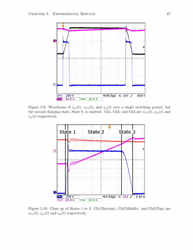
Chapter 5. Experimental Results 67
Figure 5.9: Waveforms of iLv(t), vCv(t), and iin(t) over a single switching period, butthe second charging state, State 8, is omitted. Ch1, Ch2, and Ch3 are vCv(t), iLv(t) andiin(t) respectively.
Figure 5.10: Close up of States 1 to 3. Ch1(Bottom), Ch2(Middle), and Ch3(Top) arevCv(t), iLv(t) and iin(t) respectively.

Chapter 5. Experimental Results 68
ILv Iin VCvStart of Expected Measured Expected Measured Expected MeasuredState 1 -31.6A -28.8A 27.3 27.2A 0V -16VState 2 -26.0A -28.8A 27.3 27.2A 968V 1110VState 3 22.8A 16.8A 22.3A 22.8A 968V 972VState 4 -31.6A 28.8A 22.3A 22.4A 0V -16V
Table 5.5: Comparison of measured and theoretical initial conditions for iLv(t) and vCv(t).
2. Measured and Theoretical values differ for the duration of State 1, τ1, as shown in
Table 5.4
3. Resonant Capacitor Voltage, vCv(t), overshoots Vout as apparent in Figure 5.9 and
5.10
The discrepancy between the measured and expected value of iLv(t) at the beginning
of State 3 is discussed first. In Figure 5.10, the waveforms of the converter should
transition from State 2 to State 3 when iLv(t) intersects with the input current, iin(t).
When measured, the two waveforms are 6A apart. The main reason is due to the tracking
error of the current sensors. With a bandwidth of 100kHz, the expected output of the
sensor when tracking the ramp rate of iLv(t) during State 2 is iLv(t) - 3.2A. At the same
time, iin(t) is decreasing at a constant rate, and the sensor would output the signal iin(t)
+ 0.3A. The resulting difference between the actual currents should be at maximum
2.5A, and is attributed to dc offsets in the sensors.
The second issue is that the duration of τ1 does not match the theoretical value. τ1 is
elongated in the experiment due to the fall time of the IGBT, which is given as 0.18µs
from its datasheet. The length of the fall time is over one third the theoretical duration
of State 1, which is 0.41 µs. As a consequence, ZVS is not achieved for the full duration
of the IGBT’s turn “off”.
Part of the IGBT’s turn “off” still occurs under ZVS. Two intervals exist during the
IGBT turn “off” transition, the turn “off” delay and the fall time. The turn “off” delay
is the time it takes for the collector current of the IGBT to reach 90% of its on state

Chapter 5. Experimental Results 69
current after the gate signal is removed. During this period, the majority of the IGBT
current does not change. The fall time is defined as the time it takes for the current of
the IGBT to fall from 90% to 10%.
For the proposed converter, ZVS is not achieved for the complete turn “off” of the
IGBT. However, between the turn “off” delay and fall time, the fall time is the dominant
source of switching losses of the two turn “off” intervals. During the turn “off” delay
the current conducted by the IGBT does not change much during the delay, and the
converter continues to operates as if it is in State 4 or 8. Thus, most of this period of
the IGBT turn “off” still achieves ZVS. During the fall time, the current conducted by
the IGBT begins to decrease, and iLv(t) is redirected into Cv. Thereby initiating State 1
or State 5 while the IGBT is still turning “off”, and resulting in switching losses.
The third concern is that the resonant capacitor voltage, vCv(t), overshoots Vout. This
was previously discussed in Section 2.3, and is expected. vCv(t) overshoots Vout because
of the forward recovery of the rectifying diode, Drect. Thus, the diode has a hard turn
“on”, and causes minor ringing in the circuit.
5.3.2 Efficiency
The efficiency curves of the experimental converter are presented in this section. Shown
in Figure 5.11 and 5.12 are the efficiency curves for different conversion ratios. The
first figure plots the efficiency against the input current since losses are assumed to be
dominated by conduction loss. The second figure plots the efficiency against output
current to compare the efficiency curves at equal output power. For these curves, Vout
was set to 1kV, and none of the passive components were changed from curve to curve.
As a result, components like the input inductor, Lin, and resonant inductor, Lv, are
overrated, and the conduction loss is somewhat lower than a properly rated inductor,
but core loss is higher. As expected, lower conversion ratios allow for higher efficiency,
and the efficiency for this prototype typically peaks around an Iin of 30A.

Chapter 5. Experimental Results 70
Figure 5.11: Efficiency curves for step-up ratios of 5, 8.3 and 10 plotted against inputcurrent.
Figure 5.12: Efficiency curves for step-up ratios of 5, 8.3 and 10 plotted against outputcurrent.

Chapter 5. Experimental Results 71
To compare the theoretical efficiency to the measured efficiency, the converter was
operated with an input voltage of 100V at a 1:10 step up ratio using the components
of Table 5.2. Figure 5.13 shows resulting theoretical and measured efficiency curves. A
difference of 3.5% or greater was measured between the theoretical and experimental
curves.
To investigate the losses, the converter was set to deliver 2.37kW with two different
parameter sets listed in Table 5.6. The major difference is that parameter set 1 uses a
Cv of 25nF and parameter set 2 uses a Cv of 100nF.
ValueConverter Property Parameter Set 1 Parameter Set 2
Vin 100V 100VVout 1kV 1kVfsw 1.7kHz 1.4kHzPout 2.37kW 2.37kWLin 5 mH 5mHLv 500 µH 500 µHCv 25 nF 100 nF
Table 5.6: Converter operating point used to investigate efficiency.
In the theoretical efficiency calculation, the only losses that have been accounted
for are conduction losses. The two most plausible sources of loss are core losses in the
magnetics, and switching losses. Regarding switching losses, Section 5.3.1 highlighted
that the turn “off” of the IGBT would produce loss. Another source of switching loss is
the turn “on” sequence for the rectifying diode,Drect.
IGBT Switching Loss
In Section 5.3.1, it was deduced that the IGBT turn “off” caused losses due to the short
duration of State 1 compared to the fall time for the IGBT. The current in each IGBT
could not be measured to estimate turn “off” loss. Therefore, the duration of State 1 was
extended by increasing the resonant capacitor, Cv. The theoretical duration of State 1

Chapter 5. Experimental Results 72
Figure 5.13: Theoretical and Actual Efficiency Curves at a step-up ratio of 10:1.
was lengthened by 1.1µs increasing the expected τ1 from 0.4 µs to 1.5 µs by changing Cv
from 25nF to 100nF.
When tested, the measured duration of State 1 increased from 1.1µs to 2.2µs. The
duration still does not match the theoretical value, but it did increase by 1.1µs, which
matches the expected change in τ1. Efficiency was found to increase despite increased
resonant inductor conduction losses that resulted from the change in Cv. Figure 5.14
shows the experimental efficiency for the two values of Cv.
The efficiency of the operating point under analysis is shown to improve by nearly a
percent, even though its expected efficiency has been reduced, as can be seen by compar-
ing Figure 5.15 and 5.13. Figure 5.15 also shows better agreement between the theoretical
and experimental efficiency curves than Figure 5.13.

Chapter 5. Experimental Results 73
Figure 5.14: These curves compare the two different efficiencies achieved with a Cv of25nF and 100nF
Figure 5.15: Theoretical and Actual Efficiency Curves for Cv = 100nF with a step-upratio of 1:10.

Chapter 5. Experimental Results 74
Diode Switching Loss
The rectifying turn “on” loss is not unique to this converter, thus the calculation method
has been placed in Appendix C. The rectifying diode turn “on” loss was found by
assuming the diode was fully conducting by the peak of the voltage overshoot. The
calculated loss of the rectifying diode turn on was 3.4W for the converter with Cv of
100nF. This represents only 0.1% loss at the investigated operating point.
Magnetic Loss
The magnetic loss had to be found experimentally due to lack of information. Loss
was found by recording temperature rise and is detailed in Appendix B. The resonant
inductor’s loss was not significant enough to measure, but the input inductor’s core loss is
estimated to be 40.9W and represents a loss of 1.6% for the converter with Cv of 100nF.
Power Loss Summary
A summary of power loss is presented in Table 5.7. This breakdown is for the converter
operating with a Cv of 100nF as specified in Table 5.6.
Power (W) Percentage of PinPout 2366.8 W 89.92%
IGBT Conduction Loss 116.8 W 4.44%IGBT - Diode Conduction Loss 19.9 W 0.76%Rectifying Diode Turn-on Loss 4.9 W 0.13%
Rectifying Diode Conduction Loss 7.4 W 0.28%Cv Conduction Loss 0.1 W NegligibleCout Conduction Loss 5.8 W 0.22 %Lin Conduction Loss 13.0 W 0.49%Lv Conduction Loss 22.0 W 0.84%
Lin Core Loss 40.9 W 1.56%Unaccounted Loss 34.4 W 1.37%
Table 5.7: Breakdown of Power for Operating Point indicated in Figure 5.15 for Pin of2632.0 W.
Unaccounted losses could be attributed to many different sources like the core losses

Chapter 5. Experimental Results 75
from Lv, unaccounted core loss from Lin, inductive heating of metal surrounding the
converter, and unaccounted switching losses, which were reduced but not eliminated by
increasing Cv.
5.4 Summary and Comparison
From the experimental setup, the analysis has been verified and efficiency curves have
been measured. For a step up ratio of 1:10, a peak efficiency of 89.9% is achieved. From
the experimental setup, an additional constraint on the length of State 1 is required to
reduce switching losses at the IGBT turn “off”, which roughly proportional to Cv.
5.4.1 Boost Comparison
The current-based resonant converter can be compared to an equivalent medium voltage
boost converter using 6.5kV IGBTs from Infineon. The converters are to operate at
an input voltage of 360V at a 1 to 10 step-up, and maximum input current of 625A.
Switching losses of the boost converter are included in the efficiency estimate, with a
relatively low switching frequency of 1kHz selected to constrain switching losses [9]. The
inductor is sized for 20% ripple and the sizing of the parasitic resistance for the inductor
is based on the LR
ratio of the input inductor used in the experimental setup.
The current-based resonant converter was assumed to operate without switching loss,
and τ1 was chosen to be approximately 5x larger than the IGBT fall time when the
converter is operated at full load to satisfy this assumption. This constraint is based on
the experimental sizing of Cv in Section 5.3.2.
For the current-based resonant converter. The ripple on the input current is set by
the relative size of Lin and Lv. Since a minimum ratio of 10:1 between Lin and Lv
is required, an input ripple from average to peak of approximately 10% results. The
parasitic resistances of the inductors are based on the LR
ratios of the inductors used in

Chapter 5. Experimental Results 76
the experimental setup.
Component sizes, and details on the efficiency calculation can be found in Appendix D.
The efficiency curve comparison between the boost converter and current-based resonant
converter is shown in Figure 5.16
Figure 5.16: Comparison of Theoretical Efficiency between Boost Converter and Current-Based Resonant Converter
Figure 5.16 shows the proposed converter is able to outperform a standard boost
topology. However, magnetic and switching losses of the current based resonant con-
verter have not been included due to the lack of core material information and access
to individual switches. Magnetic losses of the proposed converter would also apply to
the boost converter. Switching loss for the IGBT fall time are not included, but switch-
ing losses for the boost converter are also a conservative estimate based upon a switch
temperature of 25C. Therefore, the current-based resonant converter is expected to
outperform an equivalent boost converter.

Chapter 5. Experimental Results 77
5.4.2 Voltage-Based Resonant Converter Comparison
The comparison between the current-based resonant converter and the voltage-based res-
onant converter of [1] should also be performed. The experimental system specifications
used in [1] are presented in Table 5.8, and specifications for the current-based resonant
converter used for comparison are presented in Table 5.9. Figure 5.17 shows the com-
parison of the efficiency curves of the two converter types. The efficiency curves show
that the voltage-based resonant converter has a more consistent efficiency across the load
range, while the current-based resonant converter is able to achieve higher efficiencies at
higher loads.
Vin 115VVout 620VLres 500µHCres 10µF
Input Power 5kW
Table 5.8: Converter Specifications from [1]
Vin 200VVout 1000VLin 5mHLv 500 µHCv 25nF
Table 5.9: Current-Based Resonant Converter Component Values and Operating Pointfor Comparison to [1]
The efficiency of the voltage-based resonant converter is limited by its switching
component. It requires voltage bidirectional two-quadrant switches, where an IGBT and
diode are used in series. Thyristors can be used for the voltage-based resonant converter,
however the maximum switching frequency will be limited by the thyristor turn “off”
time, and larger resonant components would be required. In contrast, the current-based
resonant converter is able to better utilize the V-I characteristics of IGBTs. The current-

Chapter 5. Experimental Results 78
Figure 5.17: Comparison of Theoretical Efficiency between Voltage-Based and Current-Based Resonant Converter
based resonant converter also utilizes smaller component sizes, but requires an additional
input inductor. However, this input inductor is only required to handle DC currents
allowing its cost and size to be optimized.
An important quality of [1] is that it is potentially a modular converter. Voltage
capabilities can be increased by simply adding additional switching modules, and [1]
shows that static voltage sharing is possible. However, during the switching instances,
the transient voltage across each module may exceed the switch’s rating, and further
research is required.
For the current-based resonant converter, additional switching modules could be
added, but the parasitic inductance between the modules and the rectifying diode would
increase.
Using two switching modules in series allows a limited increase in the parasitic induc-
tance. Simulation shows equal voltage balancing is achievable with ideal components.

Chapter 5. Experimental Results 79
Component mismatch, parasitic capacitance of IGBTs, and switching signal delays cause
oscillations in the voltage across the modules, but the oscillations appear to be bounded
for a two module converter. Appendix E details the preliminary simulations. The multi-
module version of the current-based resonant converter shows promise in sharing voltage
between modules without the need for active voltage balancing techniques, however pre-
liminary analysis shows that parasitic inductance will severely limit the number of series
modules.
The switching module of the voltage-based resonant converter was developed into a
family of converters in [1]. Considering the waveforms and preliminary investigations of
the current-based resonant converter, an equivalent step-down topology equivalent to a
buck converter can be developed, and it is presumed that an equivalent current-based
family of converters exists.
5.4.3 Limitations
The current-based resonant converter is a topology that can utilize IGBT technology,
allowing for faster switching frequencies and smaller tank components. From the com-
parisons, and experimental setup, additional design constraints can be added to those
developed in Section 4.5. These additional constraints are based on the assumption that
inductor resistance scales with inductor size. All the constraints or limitations are listed
as follows:
1. The ratio of the resonant inductor,Lv, to input inductor, Lin, is used to satisfy
input ripple constraint and maintain the constant input current assumption.
2. IGBT turn “off” losses can be reduced by choosing an appropriate duration, τ1,
for State 1. τ1 can be set using the resonant capacitor, Cv, which is roughly
proportional to τ1. However, a larger Cv would also result in higher conduction
losses.

Chapter 5. Experimental Results 80
3. The ratio of Cv to Lv is used to minimize conduction loss by reducing the resonant
current, Ires. However, increasing Lv and Lin may reduce efficiency by increasing
parasitic resistance.
4. The size of Lv is used to either set the frequency of operation or to set Ires for a
given Cv.
5. Cv is limited by dvdt
rating and not the RMS current rating.

Chapter 6
Conclusion
This research identified a need for efficient high voltage high step-up converters to in-
terconnect DC power systems. To address this problem, a transformerless high step-up
DC/DC converter was presented in this work. The proposed converter is based on [1],
and was referred to as a current-based resonant converter within this work.
The steady state and dynamic models for the proposed converter were presented
and verified against a PSCAD/EMTDC simulation. The analytic models were shown
to well approximate the simulation. From the dynamic model, a method of control was
developed to manage the nonlinear aspects of the model, and simulation was used for
verification.
A refinement to the analytic model was made to improve upon the solution found
through energy balance and was shown to better capture the actual current stresses of
the components. The proposed system was realized as a 100V:1kV/4kW experimental
setup. The experimental waveforms and losses were analyzed to better understand the
limitations of the converter.
In comparison to [1], the proposed converter was found to better utilize the V-I
characteristics of IGBT technology, and would be able to operate at higher switching
frequencies and reduce component size. The current-based resonant converter was shown
81

Chapter 6. Conclusion 82
to outperform the voltage-based resonant converter in efficiency at higher loads. The
proposed converter was also compared to a boost converter and was shown to provide
higher efficiency over the operating range. Based on these comparisons, the current-
based resonant converter shows promise to operate at high voltage and high gain as a
DC interconnect.
6.1 Future Work
Future work is focused on expanding the capabilities of the proposed converter, and
assessing it for use as a DC interconnect.
1. Verify control methodology with a lab setup.
2. Investigate the two module extension of this topology. Preliminary simulations
show voltage sharing is possible, even with non-idealities.
3. Reference [1] developed a family of converters. The same idea can be applied to the
current-based resonant converter to develop step-down and bidirectional converters.
4. Investigate fault propagation with the family of converters, and its operation as a
node of a DC system.

Appendices
83

Appendix A
Compensator and Current Filter
Design
In this appendix, the design of the current filter and compensator used in Section 3.2
is detailed. The current filter is used to filter the ripple of iin(t) for feedback, and a
first order low-pass filter is used. The pole of the filter was selected to filter the ripple
at the lowest operating frequency. For a converter with the properties of Table 3.2 and
maximum Iin of 50A, the minimum operating frequency is 876Hz. While the minimum
switching frequency is 876Hz, the ripple has a frequency that is two times larger because
power is delivered twice during a single switching period. As a result, the pole of the
filter is chosen as 400Hz to filter a ripple of approximately 1.8kHz.
The compensator design was performed with the analytic model. The converter pa-
rameters of Table 3.2 were used with the current filter’s pole was placed at 400Hz as
discussed. A PI controller was chosen for use with gains Kp and Ki to achieve a phase
margin of 70. The compensator values of Kp, and Ki were chosen to be -1.5 and -94.25
respectively. These values are negative because the plant contains a negative itself, and
negative feedback requires the gains be negative. The resulting bode plot of the Loop
gain is shown in Figure A.1.
84

Appendix A. Compensator and Current Filter Design 85
Figure A.1: Bode Plot of Loop

Appendix B
Magnetic Loss Measurement
Magnetic losses for the two inductors were found by recording temperature rise at various
points on the inductors as indicated in Figure B. Specifications for both inductors are
shown in Table B.1. The temperature values were measured in 15 minute intervals after
the first hour and are given in Table B.2.
At the start of the test, it was suspected that Lv would be the main source of loss,
and the starting temperature was not recorded for Lin. It was then assumed that Lin
started at ambient, similar to the rest of the system.
Inductor Value Irated Manufacturer / Part Number Type WeightLin 5000µH 75A Hammond 195G75 DC 45.4kgLv 500µH 100Arms Custom - In Lab High Freq. 27.2kg
Table B.1: Inductor Specifications
Time (min.) Lv (C) Lin AmbientLoc. 1 Loc. 2 Loc. 3 Loc. 4 Loc. 5 Loc. 6
0 28.2 28.3 28.3 28.1 27.9 27.960 37.6 37.8 33.9 33.0 31.6 39.1 37 28.575 39.6 40.2 34.6 33.6 32.0 38.4 38.4 28.890 40.2 41.0 35.1 34.5 32.3 39.1 40.1 28.9
Table B.2: Temperature of various points on both inductors.
86

Appendix B. Magnetic Loss Measurement 87
Figure B.1: The different temperature measurement locations for the inductors are indi-cated here.
From the data it is apparent that core loss in Lv is not significant enough to noticeably
heat the inductor. Comparing the temperature of Location 5 to the other measurements
on Lv, it is possible that the wiring, Location 6, is heating the surrounding area. There-
fore, the measured rise in temperature is likely not caused by core loss in Lv. Of the
points measured on Lv, the aluminium bars, Location 1 and 2, rose in temperature by
approximately 11.7C in comparison to the final ambient temperature. However, this
heating only results in 0.92W of loss through the aluminium.
The temperature of Lin increases almost regularly, and rises in temperature by 11.2C
compared to the final ambient temperature at the end of the test. The rise in temperature
results in 40.9W of loss from the loss of the input inductor. Several approximations were
used to calculate the loss. The inductor’s weight used in calculation includes the wiring
and any other mounting brackets, and the specific heat capacity of the inductor’s core
material is unknown. The inductor is most likely made from electrical steel, but a specific

Appendix B. Magnetic Loss Measurement 88
heat capacity could not be found.
Using [21] as reference, the specific heat capacity for various types of steel range from
434 JkgK
to 480 JkgK
. Thus, a specific heat capacity of 434 JkgK
was used to estimate the
core loss.

Appendix C
Rectifying Diode Loss
The rectifying diode turn “on” loss can be measured by using the voltage across the
rectifying diode, which is shown in Figure C.1. Figure C.1 is the diode voltage for
operating parameter set 1 of Table C.1. The figure also shows the assumed current that
passes through the rectifying diode for this loss calculation.
The duration of the voltage overshoot is measured as 440ns, and the diode voltage
reaches a peak value of 112V from the zero crossing in 160ns. Using a theoretical value
for the current at the beginning of State 2, it was assumed that the diode current reaches
a maximum of 59.8A at turn “on”, calculated by using Equation 4.2.9. For the diode
turn “on” loss calculation, the current is assumed to stay constant once the diode is fully
turned “on”, as indicated in Figure C.1. From these assumptions, the diode turn “on”
loss for operating parameter set 1 is calculated to be 4.4W.
The rectifying diode loss can also be calculated for operating parameter set 2 assuming
that the overshoot duration does not change. The overshoot voltage is measured to be
96V, and peak diode current is calculated with Equation 4.2.9 to be 65.4A. From this
information, the rectifying diode loss for operating parameter set 2 is estimated to be
3.4W.
89

Appendix C. Rectifying Diode Loss 90
ValueConverter Property Operating Parameter Set 1 Operating Parameter Set 2
Vin 100V 100VVout 1kV 1kVfsw 1.7kHz 1.4kHzIin 26.6A 26.4APout 2.37kW 2.37kWLin 5 mH 5mHLv 500 µH 500 µHCv 0.025 µF 0.100 µF
Table C.1: Converter operating point used to investigate efficiency.
Figure C.1: Voltage across the rectifying diode with the assumed current in the diode.

Appendix D
Boost & Current-Based Resonant
Converter Efficiency
This appendix covers the efficiency calculation, and presents the component choices for
the current-based resonant converter and the boost converter comparison. Design of the
current-based resonant converter is covered first, and is followed by the boost converter
design. Both converters have an input and output voltage of 360V and 3.6kV respectively.
3.6kV was chosen such that the calculated values for energy loss per switching instance
could be used from the datasheet. Both converters use the same IGBT data, which is
displayed in Table D.1. Parasitic resistances of passive components were estimated by
maintaining LR
and 1CR
ratios from the experimental setup. The components used in the
experiment are repeated in Table D.2 for convenience.
Switch Manufacturer Voltage Current PropertiesNumber Rating Rating
Rectifier DD750S65K3T 6500V 750A VFtyp = 3V at 25CActive Switch FZ750R65KE3 6500V 750A VFtyp = 3V at 25C
Active Switch Diode FZ750R65KE3 6500V 750A VFtyp = 3V at 25C
Table D.1: Switching components used in comparison of Boost and Current-Based Res-onant Converter.
91

Appendix D. Boost & Current-Based Resonant Converter Efficiency 92
Converter Component Value Parasitic Resistance XR
at 60 HzLv 500 µH RLv = 13.37mΩ 14Cv 0.025 µF RCesr = 37.6mΩ 2.8e6Lin 5mH RLin = 18.6mΩ 101
Table D.2: Experimental Component Properties
D.1 Current-Based Resonant Converter
The loss calculation for the resonant converter is calculated with the method described in
Section 4.4, and only accounts for conduction losses. Components were chosen iteratively,
with the input inductor, Lin, constrained to be 10x larger than the resonant inductor,
Lv. Lv was used to set the resonant current, Ires such that S1 and S2 would conduct the
switch’s rated current during the input inductor charging states, State 4 and State 8.
To achieve low switching losses, the resonant capacitor, Cv, was used to constrain the
duration , τ1, of State 1. τ1 was set to be 5x larger than the fall time of the IGBT when
the converter is operating at rated input current. Therefore, τ1 is restricted to be at least
2µs in duration for the selected IGBTs. The resulting component values are shown in
Table D.3
Converter Quantity ValueIin 625A
∆iinavg−pk 66.6 AIres 250ALin 1.7mHLv 170 µHCv 0.82 µFRLin 4.5 mΩRLv 4.5 mΩRCesr 1.1 mΩτ1 2.0µs
fsw Min. 655 HzηRes at Iinrated 94.9%
Table D.3: Current-Based Resonant Converter Component Properties and OperatingPoint

Appendix D. Boost & Current-Based Resonant Converter Efficiency 93
D.2 Boost Converter
The efficiency of the boost converter was calculated by including conduction and switch-
ing losses. For conduction losses, the efficiency can be calculated with
ηConduction =
(1− Vf
Vin
)(1
1 + RLRLoad(1−D)2
)(D.2.1)
Switch conduction loss is accounted for in the first term where Vf is the voltage drop due
to the IGBT and diode since they have identical Vf and one is conducting at all times.
The second term is due to the conduction losses of the inductor parasitic resistance.
Switching losses from the IGBT and output diode were both included in efficiency
calculations. IGBT turn “on” and turn “off” losses were calculated using Equation D.2.2,
and D.2.3 respectively. The IGBT switching losses were assumed to scale with the input
current. Thus, the maximum switch current, IswMAX , is used to normalize the turn “on”
and turn “off” energy. The input current ripple also affects the amount of current the
IGBT conducts during switch transitions, therefore the ripple, ∆Iin is included in the
switching loss estimate. The diode reverse recovery loss was included by using Equation
D.2.4.
The energy lost during the turn “on”, EIGBTTurn−on, and turn “off”, EIGBTTurn−off ,
transitions were found from the IGBT’s datasheet, and is provided in Table D.4. The
reverse recovery charge, Qrr, of the diode is also included in Table D.4.
Switching Losses ValueEIGBTTurn−on 4.2J at 25C and VCE of 3.6kVEIGBTTurn−off 3.6J at 25C and VCE of 3.6kV
Qrr 850 µC at 25C
Table D.4: Switching losses for switches used in comparison.

Appendix D. Boost & Current-Based Resonant Converter Efficiency 94
PLossTurn“on” = fswEIGBTTurn−onIswMAX
(Iin −∆Iin) (D.2.2)
PLossTurn“off” = fswEIGBTTurn−off
IswMAX
(Iin + ∆Iin) (D.2.3)
PLossQrr = fswQrrVout (D.2.4)
The component parameters and the operating point at rated output power is sum-
marized in Table D.5.
Converter Quantity valueIinrated 625A∆Iin 125 ALBoost 1.3mHRLBoost 4.8 mΩD 0.9f 1 kHz
ηBoost at Iinrated 94.9%
Table D.5: Boost Converter Component Properties and Operating Point

Appendix E
Current-Based Resonant Converter:
Voltage Sharing
This appendix details the preliminary investigation for the two module current-based
resonant converter. The circuit diagram of the two module converter is shown in Figure
E.1. For this investigation, the converter was simulated with the operating point and
components listed in Table E.1.
Two cases were simulated for the converter. One simulation compares the voltage
sharing of the modules due to mismatch in resonant inductors, and the second simulation
added parasitic capacitance of the switches, and delayed gating signals in addition to the
mismatch in resonant inductors. For an output voltage of 2kV , Vm1 and Vm2 should
ideally have a maximum value of 1kV.
Results of first simulation case with the mismatch between Lv1 and Lv2 are shown in
Figure E.2. The two modules are shown to provide a mismatch in voltage sharing, but
does not differ significantly from the expected value.
The result of the second simulation case is presented in Figure E.3. This simulation
adds parasitic capacitances of 0.5 nF across each IGBT, and a gate delay of 0.4µs between
switching module 1 and switching module 2. This means that S1 of switching module 1
95
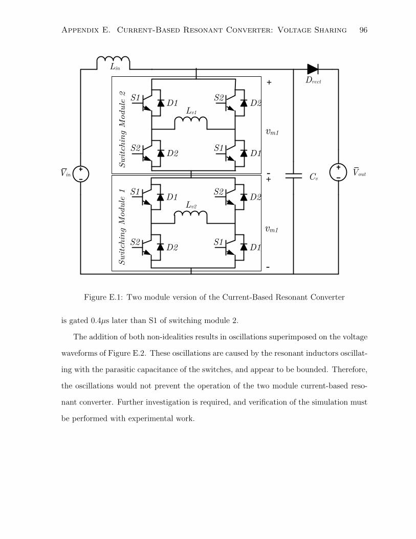
Appendix E. Current-Based Resonant Converter: Voltage Sharing 96
Switchin
g M
odule 2
Switchin
g M
odule 1
Vin
Lres
Vout
D1
Switching Module 1
Switching Module 2
+
-vm2
+
-
vm1
Vin
Lres
Vout
D1
Switching
Module 1
Switching
Module 2
+
-Vm2
+
-
Vm1
Cp
Vin
Lin
Lv1
Vout
Drect
Cv
D1S1
D2S2
D1S1
D2S2
Lv2
D1S1
D2S2
D1S1
D2S2
+
-
vm1
+
-
vm1
Figure E.1: Two module version of the Current-Based Resonant Converter
is gated 0.4µs later than S1 of switching module 2.
The addition of both non-idealities results in oscillations superimposed on the voltage
waveforms of Figure E.2. These oscillations are caused by the resonant inductors oscillat-
ing with the parasitic capacitance of the switches, and appear to be bounded. Therefore,
the oscillations would not prevent the operation of the two module current-based reso-
nant converter. Further investigation is required, and verification of the simulation must
be performed with experimental work.

Appendix E. Current-Based Resonant Converter: Voltage Sharing 97
Converter Quantity valueVin 200VVout 2kVfsw 3.5kHzLin 5mHLv1 225µHLv2 250µHCv 0.1µF
Table E.1: Components of the two module Current-Based Resonant Converter
Figure E.2: Voltage sharing between modules of Two Module Current-Based ResonantConverter with mismatch between Lv components.

Appendix E. Current-Based Resonant Converter: Voltage Sharing 98
Figure E.3: Voltage sharing between modules of Two Module Current-Based ResonantConverter. The following non-idealities have been added: mismatch between Lv compo-nents, delay in gating signals, and parasitic capacitance.

Bibliography
[1] A. Hagar, “A new family of transformerless modular dc-dc converters for high power
applications,” Ph.D. dissertation, University of Toronto, 2010.
[2] D. Jovcic, “Step-up dc-dc converter for megawatt size applications,” Power Elec-
tronics, IET, vol. 2, no. 6, pp. 675 –685, 2009.
[3] J. Ciezki and R. Ashton, “Selection and stability issues associated with a navy
shipboard dc zonal electric distribution system,” Power Delivery, IEEE Transactions
on, vol. 15, no. 2, pp. 665 –669, apr 2000.
[4] K. Mizuguchi, S. Muroyama, Y. Kuwata, and Y. Ohashi, “A new decentralized
dc power system for telecommunications systems,” in Telecommunications Energy
Conference, 1990. INTELEC ’90., 12th International, oct 1990, pp. 55 –62.
[5] C. Kim, V. Sood, G. Jang, S. Lim, and S. Lee, HVDC transmission: power conver-
sion applications in power systems. John Wiley & Sons, 2009.
[6] D. Nilsson and A. Sannino, “Efficiency analysis of low- and medium- voltage dc
distribution systems,” in Power Engineering Society General Meeting, 2004. IEEE,
june 2004, pp. 2315 –2321 Vol.2.
[7] M. Saeedifard, M. Graovac, R. Dias, and R. Iravani, “Dc power systems: Challenges
and opportunities,” in Power and Energy Society General Meeting, 2010 IEEE, july
2010, pp. 1 –7.
99

Bibliography 100
[8] D. Jovcic and B. Ooi, “Developing dc transmission networks using dc transformers,”
Power Delivery, IEEE Transactions on, vol. 25, no. 4, pp. 2535 –2543, oct. 2010.
[9] N. Denniston, A. Massoud, S. Ahmed, and P. Enjeti, “Multiple module high gain
high voltage dc-dc transformers for offshore wind energy systems,” Industrial Elec-
tronics, IEEE Transactions on, 2010.
[10] D. Jovcic and B. T. Ooi, “Tapping on hvdc lines using dc transformers,” Electric
Power Systems Research, vol. 81, no. 2, pp. 561 – 569, 2011. [Online]. Available:
http://www.sciencedirect.com/science/article/pii/S0378779610002609
[11] W. Li, Y. Zhao, Y. Deng, and X. He, “Interleaved converter with voltage multi-
plier cell for high step-up and high-efficiency conversion,” Power Electronics, IEEE
Transactions on, vol. 25, no. 9, pp. 2397 –2408, 2010.
[12] K. Tseng and T. Liang, “Novel high-efficiency step-up converter,” Electric Power
Applications, IEE Proceedings -, vol. 151, no. 2, pp. 182 – 190, Mar. 2004.
[13] J.-M. Kwon and B.-H. Kwon, “High step-up active-clamp converter with input-
current doubler and output-voltage doubler for fuel cell power systems,” Power
Electronics, IEEE Transactions on, vol. 24, no. 1, pp. 108 –115, 2009.
[14] D. Vinnikov, J. Laugis, and I. Galkin, “Middle-frequency isolation transformer de-
sign issues for the high-voltage dc/dc converter,” in Power Electronics Specialists
Conference, 2008. PESC 2008. IEEE, 2008, pp. 1930 –1936.
[15] J. Liu, L. Sheng, J. Shi, Z. Zhang, and X. He, “Design of high voltage, high power and
high frequency transformer in lcc resonant converter,” in Applied Power Electronics
Conference and Exposition, 2009. APEC 2009. Twenty-Fourth Annual IEEE, 2009,
pp. 1034 –1038.

Bibliography 101
[16] M. Perez, C. Blanco, M. Rico, and F. Linera, “A new topology for high voltage, high
frequency transformers,” in Applied Power Electronics Conference and Exposition,
1995. APEC ’95. Conference Proceedings 1995., Tenth Annual, no. 0, Mar. 1995,
pp. 554 –559 vol.2.
[17] D. M. Robert W. Erickson, Fundamentals of Power Electronics, Second Edition.
New York : Kluwar Academic, 2004.
[18] R. Withanage, W. Crookes, and N. Shammas, “Novel voltage balancing technique
for series connection of igbts,” in Power Electronics and Applications, 2007 European
Conference on, sept. 2007, pp. 1 –10.
[19] B. Baha and M. O. Tokhi, “Dynamic modelling and con-
trol of resonant switch mode converters,” Control Engineering Prac-
tice, vol. 5, no. 11, pp. 1533 – 1542, 1997. [Online]. Available:
http://www.sciencedirect.com/science/article/pii/S0967066197100077
[20] C. Hahn, “Modeling and control design for high power resonant dc-dc converter
topologies,” Department of Electrical and Computer Engineering, University of
Toronto and Institute of Electrical Power Systems of the University of Erlangen-
Nuremberg, Tech. Rep., 2011, studienarbeit.
[21] F. Incropera and D. DeWitt, Fundamentals of heat and mass transfer. John Wiley,
2007.
Related Documents


![A Buck Boost Transformerless DC–DC Converter Based on … · 1 School of Engineering, Computing and Mathematics,Oxford Brookes University, Wheatley campus, ... In [11] a study dedicated](https://static.cupdf.com/doc/110x72/603dd271fe60e17e817595e3/a-buck-boost-transformerless-dcadc-converter-based-on-1-school-of-engineering.jpg)