S1 Supporting Information Quantitatively Enhanced Reliability and Uniformity of High‐κ Dielectrics on Graphene Enabled by Self‐Assembled Seeding Layers Vinod K. Sangwan 1 , Deep Jariwala 1 , Stephen A. Filippone 1# , Hunter J. Karmel 1 , James E. Johns 1 , Justice M. P. Alaboson 1 , Tobin J. Marks 1,2 *, Lincoln J. Lauhon 1 *, Mark C. Hersam 1,2,3 * 1 Department of Materials Science and Engineering, Northwestern University, Evanston, Illinois 60208 2 Department of Chemistry, Northwestern University, Evanston, Illinois 60208 3 Department of Medicine, Northwestern University, Evanston, Illinois 60208 *t‐[email protected]; [email protected]; m‐[email protected] # Present address: Department of Materials Science and Engineering, Johns Hopkins University, Baltimore, MD, 21218 Section S1: Dielectric Growth a. Graphitization of SiC: Capacitors were fabricated on epitaxially grown graphene on n‐type (nitrogen doped, resistivity = 0.013 – 2 ohm‐cm) 4H‐SiC (0001) substrates (Cree, Inc.). EG‐SiC was chosen over CVD graphene due to the atomic level smoothness of the sample over large areas, which minimizes the extrinsic effects of surface roughness. The SiC wafers were first diced into 9 mm x 4.5 mm substrates (American Precision Dicing) and cleaned via ultra‐sonication in acetone and isopropanol. The substrates were then loaded

Welcome message from author
This document is posted to help you gain knowledge. Please leave a comment to let me know what you think about it! Share it to your friends and learn new things together.
Transcript

S1
Supporting Information
Quantitatively Enhanced Reliability and Uniformity of High‐κ
Dielectrics on Graphene Enabled by Self‐Assembled Seeding Layers
Vinod K. Sangwan1, Deep Jariwala1, Stephen A. Filippone1#, Hunter J. Karmel1, James E. Johns1, Justice M. P. Alaboson1, Tobin J. Marks1,2*, Lincoln J. Lauhon1*, Mark C. Hersam1,2,3*
1Department of Materials Science and Engineering, Northwestern University, Evanston, Illinois 60208
2Department of Chemistry, Northwestern University, Evanston, Illinois 60208
3Department of Medicine, Northwestern University, Evanston, Illinois 60208
*t‐[email protected]; [email protected]; m‐[email protected]
# Present address: Department of Materials Science and Engineering, Johns Hopkins University,
Baltimore, MD, 21218
Section S1: Dielectric Growth
a. Graphitization of SiC:
Capacitors were fabricated on epitaxially grown graphene on n‐type (nitrogen doped, resistivity
= 0.013 – 2 ohm‐cm) 4H‐SiC (0001) substrates (Cree, Inc.). EG‐SiC was chosen over CVD graphene due to
the atomic level smoothness of the sample over large areas, which minimizes the extrinsic effects of
surface roughness. The SiC wafers were first diced into 9 mm x 4.5 mm substrates (American Precision
Dicing) and cleaned via ultra‐sonication in acetone and isopropanol. The substrates were then loaded
S2
into an ultra‐high vacuum (UHV) scanning tunneling microscope (STM) chamber (base pressure ~ 5 x 10‐
11 Torr). The samples were outgassed at 550 ̊C overnight. Graphitization was achieved by direct‐
current heating of the samples at 1270 ̊C for 20 min. The samples were cooled down gradually over
several minutes. The graphitization process results in a mixture of single‐layer and bilayer epitaxial
graphene on SiC.1 Depending on the annealing conditions, graphitization of the silicon face of SiC under
UHV conditions can result in a mixture of layer numbers, n, with 0 < n < 2. Consequently, graphitization
was performed for a sufficient duration to ensure that n > 1 over the entire sample and eliminated
patches of ungraphitized 6 x 6 SiC surface. Representative X‐ray photoelectron spectroscopy
(XPS) and Raman spectroscopy (after subtracting the Raman signal from the underlying SiC substrate) of
the graphitized SiC is shown in Fig. S1. Measurement at several positions on the wafers confirmed full
graphitization.
b. Evaporation of PTCDA:
Perylene‐3,4,9,10‐tetracarboxylic dianhydride (PTCDA) (97% purity, Sigma Aldrich) was
evaporated on EG‐SiC substrates in a thermal evaporator (< 10‐6 Torr) dedicated to the evaporation of
organic compounds. The samples were slowly heated up to 150 ̊C prior to PTCDA evaporation to
facilitate the formation of large grains of PTCDA. The PTCDA powder was slowly heated in an alumina
crucible until a stable deposition rate of 0.1 Å/sec was achieved on the quartz crystal thickness monitor.
The source material was then allowed to degas for an additional 10 min to minimize contamination. A
total deposition time of 40 sec attained a nominal PTCDA thickness of 0.4‐0.5 nm (~1‐2 ML thick).
The resulting film was characterized with Raman spectroscopy and atomic force microscopy
(AFM). Raman spectroscopy allows verification of the sub‐2 ML thickness of the deposited PTCDA
layers.1 In particular, PTCDA photoluminescence is quenched by the graphene substrate when the
thickness is less than 2 MLs, whereas PTCDA films thicker than 2 MLs lead to the onset of a fluorescence
S3
background in the Raman spectra beyond 1200 cm‐1. The Raman spectra of the PTCDA evaporated on
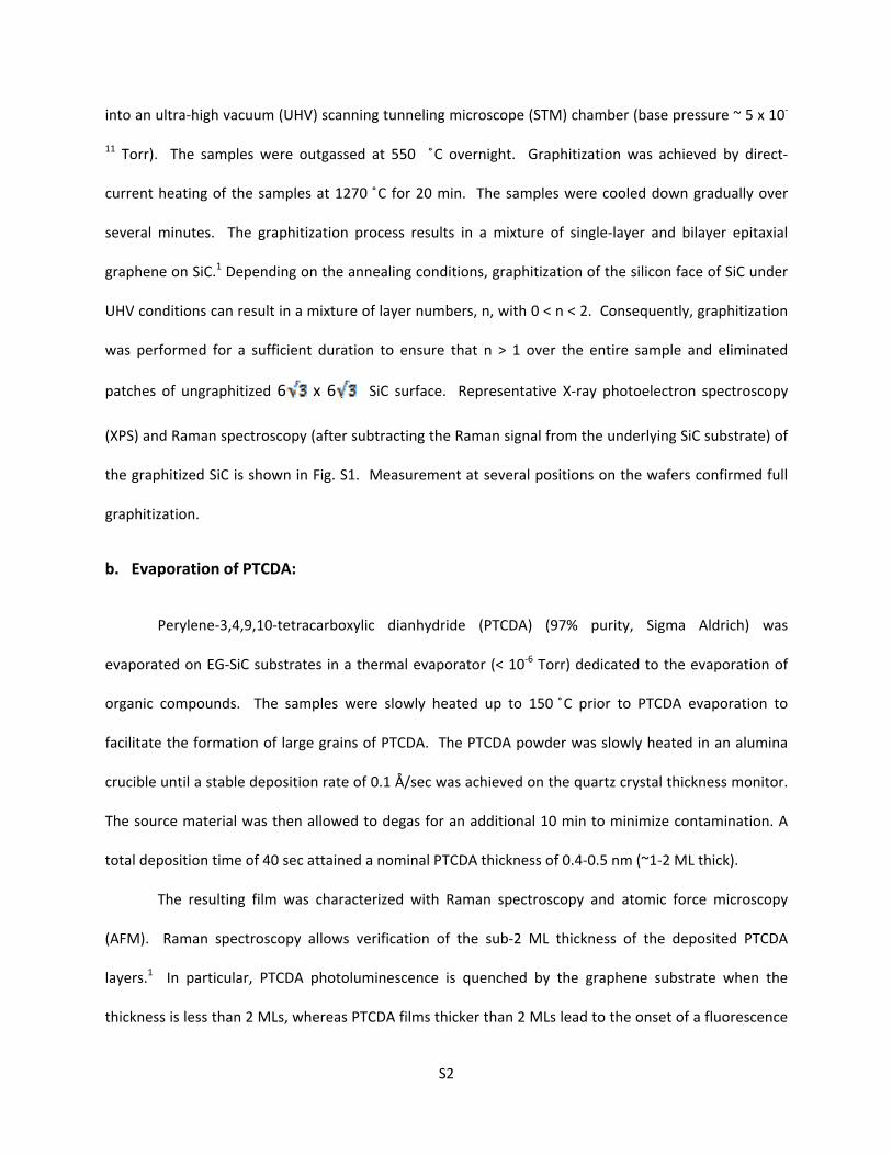
EG‐SiC samples showed an indiscernible fluorescence background (Fig. S2), which verifies the sub‐2 ML
PTCDA thickness.1 AFM images of thicker PTCDA films (> 3 MLs) showed increasingly rougher
topography due to vertical growth in segregated islands. Consequently, the observed smooth surface
morphology in the AFM images of the PTCDA‐coated EG‐SiC substrate also suggested <2 ML thickness.
Evaporation of PTCDA for less than 30 sec yielded incomplete coverage (< 1 ML). The presence of
PTCDA was also confirmed by AFM images following dielectric growth by atomic layer deposition (ALD).
ALD growth of 2 nm Al2O3 on a sub‐monolayer coverage of PTCDA led to a rougher surface morphology
(Fig. S2b) compared to Al2O3 grown on 1‐2 MLs of PTCDA (Fig. S2c), similar to that reported in Ref2.
Therefore, the optimized growth conditions produced a PTCDA coverage between 1 and 2 MLs.
a b
Figure S1. (a) X‐ray photoelectron spectroscopy (XPS) and (b) Raman spectroscopy of a graphitized 4H‐
SiC wafer. The integrated intensity from the graphitic carbon at 284.4 eV is ~ 1.6 times larger than the
sum of the integrated intensities for the buffer peaks, consistent with a mixed monolayer/bilayer film.
Raman spectra of EG‐SiC showed the characteristic G and 2D bands of graphene across the entire wafer.
The width of the 2D band was 70 ± 10 cm‐1, intermediate between previously reported values for
monolayer (60 cm‐1) and bilayer (95 cm‐1) epitaxial graphene on 4H‐SiC(0001).3
S4
Figure S2. (a) Raman spectrum of <2 ML PTCDA grown on an EG‐SiC substrate shows the absence of a
fluorescence background. (b) AFM image of 2 nm Al2O3 grown by ALD on sub‐monolayer coverage of
PTCDA. (c) AFM image of 2 nm Al2O3 grown by ALD on 1‐2 MLs of PTCDA.
c. Atomic Layer Deposition:
ALD was performed on the PTCDA‐coated EG‐SiC samples using a Savannah S100 ALD reactor
(Cambridge Nanotech, Cambridge MA). The samples were briefly exposed to air during transfer from
the thermal evaporator to the ALD reactor. The substrates were loaded into the chamber, which was
pre‐heated to 100 C̊ and then the chamber was heated up to 150 ̊C at a ramp rate of 3 ̊C/min to avoid
thermal shock perturbation of the organic seeding layer. The base pressure of the chamber was
maintained at 0.2 Torr with a constant N2 flow rate of 20 sccm. The samples were exposed to sequential
doses of the oxide precursor and deionized water interspersed with dry N2 purge steps between each
precursor dose. The precursors for Al2O3 and HfO2 films were trimethyl aluminum (TMA, Aldrich, 99%)
and tetrakis(dimethylamido)hafnium(IV) (TDEAHf, Aldrich, 99.99%), respectively. For Al2O3 growth, a
S5
single ALD cycle consisted of a TMA pulse for 0.015 s and a 15 s purge, followed by a H2O pulse for 0.015
s and a second 15 s purge. For HfO2 growth, a single ALD cycle consisted of a TDMAHf pulse for 0.25 s
and a 10 s purge, followed by a H2O pulse for 0.015 s and another 10 s purge. During growth, TMA and
TDEAHf precursor bottles were kept at room temperature and 75 ̊C, respectively. Predetermined
growth rates of 0.8 Å/cycle for Al2O3 and 0.95 Å/cycle for HfO2 were used to calculate the required
number of cycles for each oxide thickness.2
Section S2: Capacitance Measurement and Analysis
a. Capacitance‐Voltage Measurements:
Capacitance‐voltage (C‐V) measurements were conducted on area‐3 (80 µm x 80 µm) capacitors
in each sample in ambient using a HP 4192A impedance analyzer. Au pads were contacted by tungsten
cat whisker soft‐probes (Signatone, SE‐SM) to avoid accidental damage to the ultra‐thin dielectrics. C‐V
measurements were conducted on 5 capacitors distributed over ~1 mm2 area on each sample to obtain
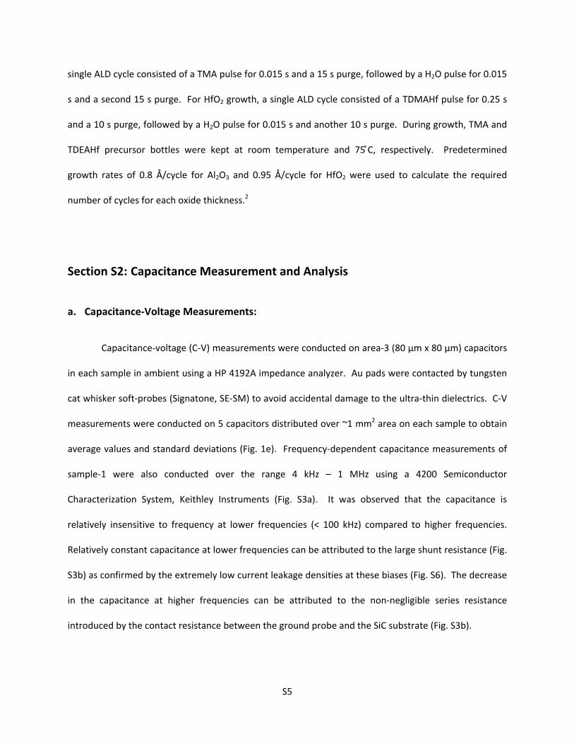
average values and standard deviations (Fig. 1e). Frequency‐dependent capacitance measurements of
sample‐1 were also conducted over the range 4 kHz – 1 MHz using a 4200 Semiconductor
Characterization System, Keithley Instruments (Fig. S3a). It was observed that the capacitance is
relatively insensitive to frequency at lower frequencies (< 100 kHz) compared to higher frequencies.
Relatively constant capacitance at lower frequencies can be attributed to the large shunt resistance (Fig.
S3b) as confirmed by the extremely low current leakage densities at these biases (Fig. S6). The decrease
in the capacitance at higher frequencies can be attributed to the non‐negligible series resistance
introduced by the contact resistance between the ground probe and the SiC substrate (Fig. S3b).
S6
Previously, we utilized a two‐frequency measurement method to extract the intrinsic
capacitance of similar capacitors on EG‐SiC.2 Here, we conduct C‐V measurements at a low frequency of
1 kHz where the measured capacitance is expected to approach the real value. Larger error bars in
sample‐3 capacitors could be due to the thickness variation in the HfO2 layer grown directly on PTCDA.
This is consistent with the increased surface roughness of HfO2 grown directly on PTCDA as reported
previously.2 The C‐V measurements of the control‐1 samples on Si substrates show large capacitance
variation near 0 V due to the formation of a depletion region in the Si substrate, Fig. S4. The capacitance
in the accumulation region (V > 1 V) is thus taken as the capacitance (Cg) of the oxide stack.
Figure S3. (a) Frequency‐dependent capacitance measurement of sample‐1 at frequencies ranging from
4 kHz to 1 MHz. (b) The equivalent RC circuit consists of a shunt resistance and series resistance.

S7
Figure S4. C‐V measurement of a control‐1 capacitor at 1 kHz.
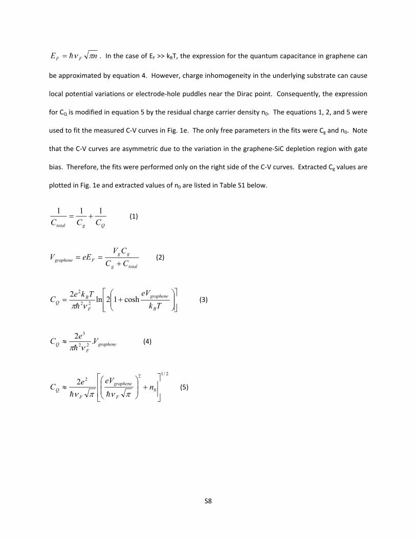
b. Quantum Capacitance Modeling:
Measured C‐V curves of the capacitors consisting of graphene at one of the electrodes have a
broad V‐shape due to the quantum capacitance of graphene. For the sake of simplicity, single‐layer
graphene was assumed instead of the single/bilayer graphene mixture. Since the oxide capacitance (500
– 800 nF/cm2) is approximately an order of magnitude lower than quantum capacitance (CQ) of
graphene at similar Fermi energies the error in the extracted capacitance is expected to be low.4 The
unique electronic structure and finite density of states in graphene at low energies results in carrier
density dependent CQ.4, 5 CQ acts in series with the gate dielectric capacitance (Cg) (Fig. S5) and thus CQ
begins to dominate the total capacitance (Ctotal) for large Cg (equation 1 below). As a result, the Fermi
level of the graphene can be modulated significantly in case of large Cg (equation 2). The analytical
expression for the quantum capacitance is given in equation 3, where kB, e, , vF, T, and Vgraphene are
Boltzmann’s constant, electronic charge, Planck’s constant, Fermi velocity of graphene, temperature,
and graphene potential, respectively. The Fermi level (EF) is related to the carrier concentration (n) by
S8
nE FF . In the case of EF >> kBT, the expression for the quantum capacitance in graphene can
be approximated by equation 4. However, charge inhomogeneity in the underlying substrate can cause
local potential variations or electrode‐hole puddles near the Dirac point. Consequently, the expression
for CQ is modified in equation 5 by the residual charge carrier density n0. The equations 1, 2, and 5 were
used to fit the measured C‐V curves in Fig. 1e. The only free parameters in the fits were Cg and n0. Note
that the C‐V curves are asymmetric due to the variation in the graphene‐SiC depletion region with gate
bias. Therefore, the fits were performed only on the right side of the C‐V curves. Extracted Cg values are
plotted in Fig. 1e and extracted values of n0 are listed in Table S1 below.
Qgtotal CCC
111 (1)
totalg
ggFgraphene CC
CVeEV
(2)
Tk
eVTkeC
B
graphene
F
BQ cosh12ln
222
2
(3)
grapheneF
Q Ve
C .2
22
3
(4)
2/1
0
222
n
eVeC
F
graphene
F
Q (5)

S9
Figure S5. Schematic of the quantum capacitance of graphene in series with the capacitance of the gate
dielectric.
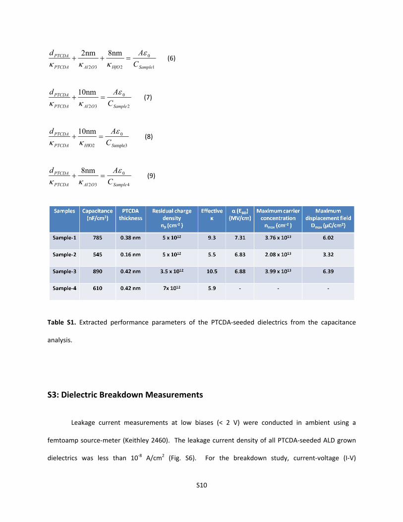
c. Extraction of Dielectric Constants:
The extracted Cg values were used to determine the dielectric constant values of the different
oxide layers as well as the thickness of the PTCDA in each sample following a model of parallel plate
capacitors in series (see equations 6‐9 below). The dielectric constant of PTCDA was taken as 1.9
(perpendicular to the plane). Simultaneous solution of equations 6‐9 yields the dielectric constants of
Al2O3 and HfO2 as 6.5 and 13, respectively, in agreement with literature precedent.2 The thickness of the
PTCDA layer is less than 0.5 nm in all samples (Table S1), in agreement with Raman spectroscopy and
AFM studies, as described in Section S1. Table S1 also includes intrinsic dielectric performance
parameters such as maximum carrier concentration (without accounting for CQ) and the Weibull scale
parameter for maximum displacement field (Dmax = κε0α(EBD), see manuscript) before dielectric
breakdown. The calculation of the Weibull scale parameter (α) for the effective breakdown field (EBD)
was performed from data for area‐3 capacitors on the sample‐1, ‐2, ‐3 and area‐5 capacitors on sample‐
4 (Section S4). Note that the quantum capacitance model fits yield only approximate values of Cg due to
the asymmetry in the C‐V curve caused by varying thickness of the depletion region. Therefore, we also
considered the measured lowest capacitance value near the Dirac point as Cg to extract PTCDA
thickness. The extracted thickness of PTCDA was found to be less than 0.9 nm in all samples.
S10
1
0
232
nm8nm2
SampleHfOOAlPTCDA
PTCDA
C
Ad
(6)
2
0
32
nm10
SampleOAlPTCDA
PTCDA
C
Ad
(7)
ample3
0
fO2
nm10
SHPTCDA
PTCDA
C
Ad
(8)
4
0
32
nm8
SampleOAlPTCDA
PTCDA
C
Ad
(9)
Table S1. Extracted performance parameters of the PTCDA‐seeded dielectrics from the capacitance
analysis.
S3: Dielectric Breakdown Measurements
Leakage current measurements at low biases (< 2 V) were conducted in ambient using a
femtoamp source‐meter (Keithley 2460). The leakage current density of all PTCDA‐seeded ALD grown
dielectrics was less than 10‐8 A/cm2 (Fig. S6). For the breakdown study, current‐voltage (I‐V)
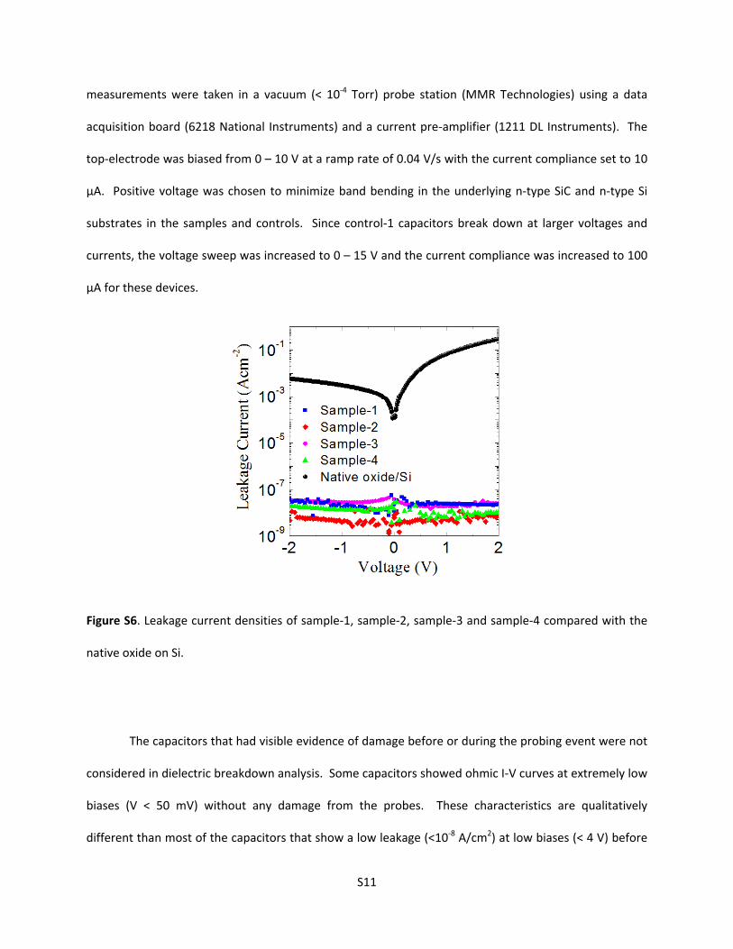
S11
measurements were taken in a vacuum (< 10‐4 Torr) probe station (MMR Technologies) using a data
acquisition board (6218 National Instruments) and a current pre‐amplifier (1211 DL Instruments). The
top‐electrode was biased from 0 – 10 V at a ramp rate of 0.04 V/s with the current compliance set to 10
µA. Positive voltage was chosen to minimize band bending in the underlying n‐type SiC and n‐type Si
substrates in the samples and controls. Since control‐1 capacitors break down at larger voltages and
currents, the voltage sweep was increased to 0 – 15 V and the current compliance was increased to 100
µA for these devices.
Figure S6. Leakage current densities of sample‐1, sample‐2, sample‐3 and sample‐4 compared with the
native oxide on Si.
The capacitors that had visible evidence of damage before or during the probing event were not
considered in dielectric breakdown analysis. Some capacitors showed ohmic I‐V curves at extremely low
biases (V < 50 mV) without any damage from the probes. These characteristics are qualitatively
different than most of the capacitors that show a low leakage (<10‐8 A/cm2) at low biases (< 4 V) before

S12
breakdown. Large leakage currents could be due to local defects from contamination or sub‐optimal
ALD growth. Such capacitors are considered for the breakdown analysis, and they termed as “leaky
capacitors.” Their numbers are listed in Table S2 for all of the samples.
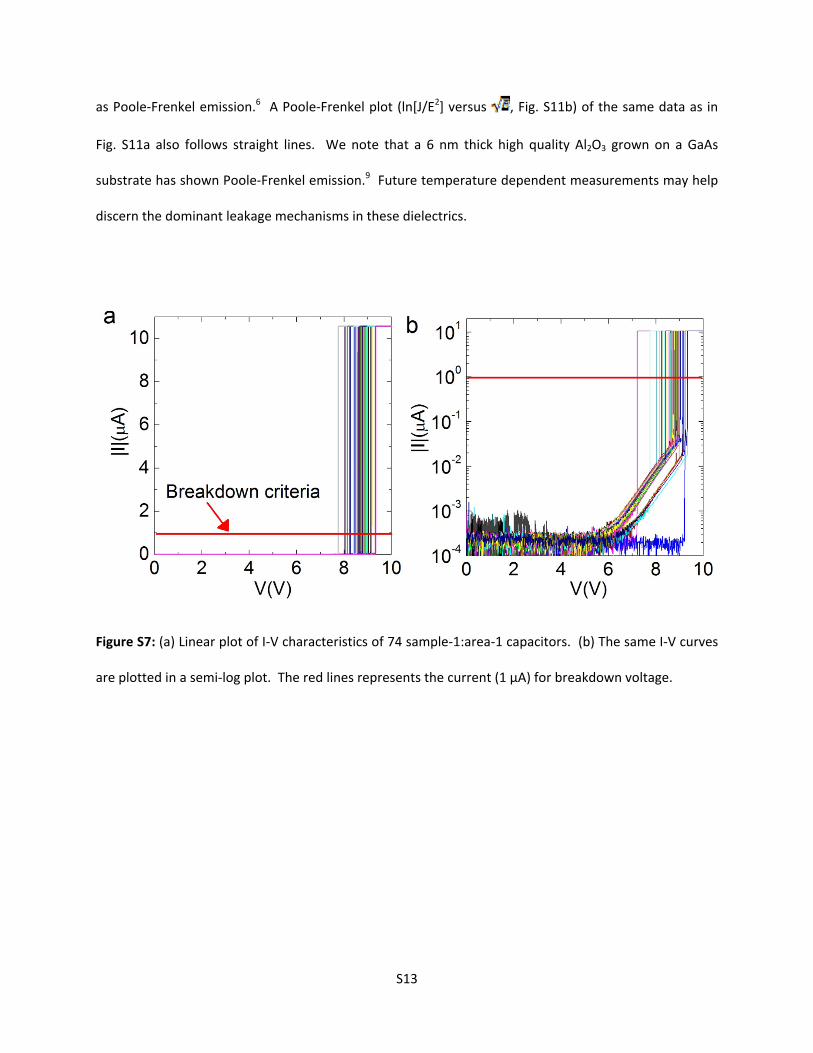
Fig. S7 and Fig. S8 show current‐voltage (I‐V) characteristics of all of the 210 capacitors
measured on the sample‐1 substrate. I‐V curves show the onset of measurable current (0.5 nA) at 6 V
and then the current continues to increase monotonically in the soft‐breakdown regime until there is an
abrupt spike in the current up to the compliance level (10 µA). This catastrophic event is called “hard‐
breakdown.” A current level of 1 µA was taken as the criterion for the breakdown voltage (VBD);
however, the reliability analysis is insensitive to the exact criterion because the sudden increase in the
current occurs within a single voltage ramp step of 0.01 V. The VBD histogram of the devices for three
sizes on the sample‐1 dielectric is plotted and fitted with the Weibull probability function in Fig. S9. As
expected, the mean VBD increases with decreasing sample area. The cumulative probability of the VBD
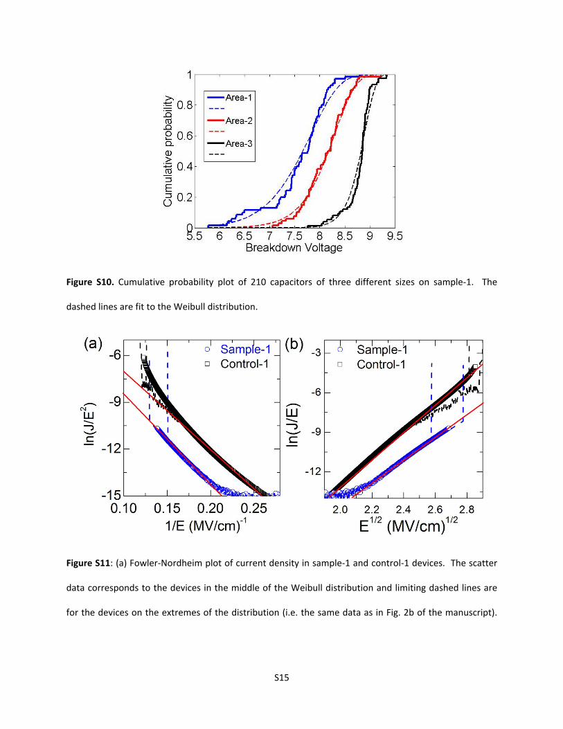
data of sample‐1 is plotted in Fig. S10.
We explored various mechanisms for current leakage preceding the hard breakdown. The
leakage current in ultra‐thin high‐κ dielectrics is commonly explained by Fowler‐Nordheim (F‐N)
tunneling.6 A Fowler‐Nordheim plot is obtained by rearranging the following equation
E
BAEJ FN exp2 , (10)
where the constants A and B depend on intrinsic materials properties such as barrier height and
electron effective mass. The F‐N plots (ln[J/E2] versus 1/E) of leakage current in sample‐1 and control‐1
devices (Fig S11a) show straight lines except for a small deviation at large fields. Although F‐N tunneling
describes our data well at low biases and is in agreement with previous reports of charge transport in
similar oxides on Si substrates7 as well as oxides on 4H‐SiC substrates,8 we note that a linear plot over
several orders of magnitude does not necessarily eliminate possibility of other leakage mechanisms such
S13
as Poole‐Frenkel emission.6 A Poole‐Frenkel plot (ln[J/E2] versus , Fig. S11b) of the same data as in
Fig. S11a also follows straight lines. We note that a 6 nm thick high quality Al2O3 grown on a GaAs
substrate has shown Poole‐Frenkel emission.9 Future temperature dependent measurements may help
discern the dominant leakage mechanisms in these dielectrics.
Figure S7: (a) Linear plot of I‐V characteristics of 74 sample‐1:area‐1 capacitors. (b) The same I‐V curves
are plotted in a semi‐log plot. The red lines represents the current (1 µA) for breakdown voltage.

S14
Figure S8: (a) I‐V characteristics of 68 sample‐1:area‐2 capacitors. (b) I‐V characteristics of 70 sample‐
1:area‐3 capacitors. The red lines represents the current (1 µA) for breakdown voltage.
Figure S9. Histogram of breakdown voltage (VBD) for area‐1, area‐2 and area‐3 capacitors on a sample‐1
substrate. Solid lines are Weibull fits to the distribution.
S15
Figure S10. Cumulative probability plot of 210 capacitors of three different sizes on sample‐1. The
dashed lines are fit to the Weibull distribution.
Figure S11: (a) Fowler‐Nordheim plot of current density in sample‐1 and control‐1 devices. The scatter
data corresponds to the devices in the middle of the Weibull distribution and limiting dashed lines are
for the devices on the extremes of the distribution (i.e. the same data as in Fig. 2b of the manuscript).

S16
Red straight line is to guide the eye. (b) Poole‐Frenkel plot of the same data as in (a). Red straight line is
to guide the eye.
Section S4: Dielectric Breakdown Analysis
First, a 5 nm Al2O3 dielectric grown on PTCDA‐coated EG‐SiC yielded 100% leaky capacitors (out
of 20 measured). Then, an 8 nm Al2O3 dielectric (sample‐4, Fig. 1c) was measured and characteristics
were found to be sub‐optimal for a large‐area reliability study (discussed below). In contrast, a 10 nm
Al2O3 dielectric exhibited leakage I‐V characteristics similar to conventional high‐κ dielectric reliability
studies in the literature; therefore, a total thickness of 10 nm was held constant in the more extensively
studied sample‐1, sample‐2, and sample‐3 (Fig. 1c). The average area of each sample capacitor was
measured from optical microscopy (Fig. S12).
Figure S12. An optical image of an area‐2 capacitor. The red line at the edge of the electrode was
automatically generated by contrast recognition in the optical microscope software to calculate the
area.
S17
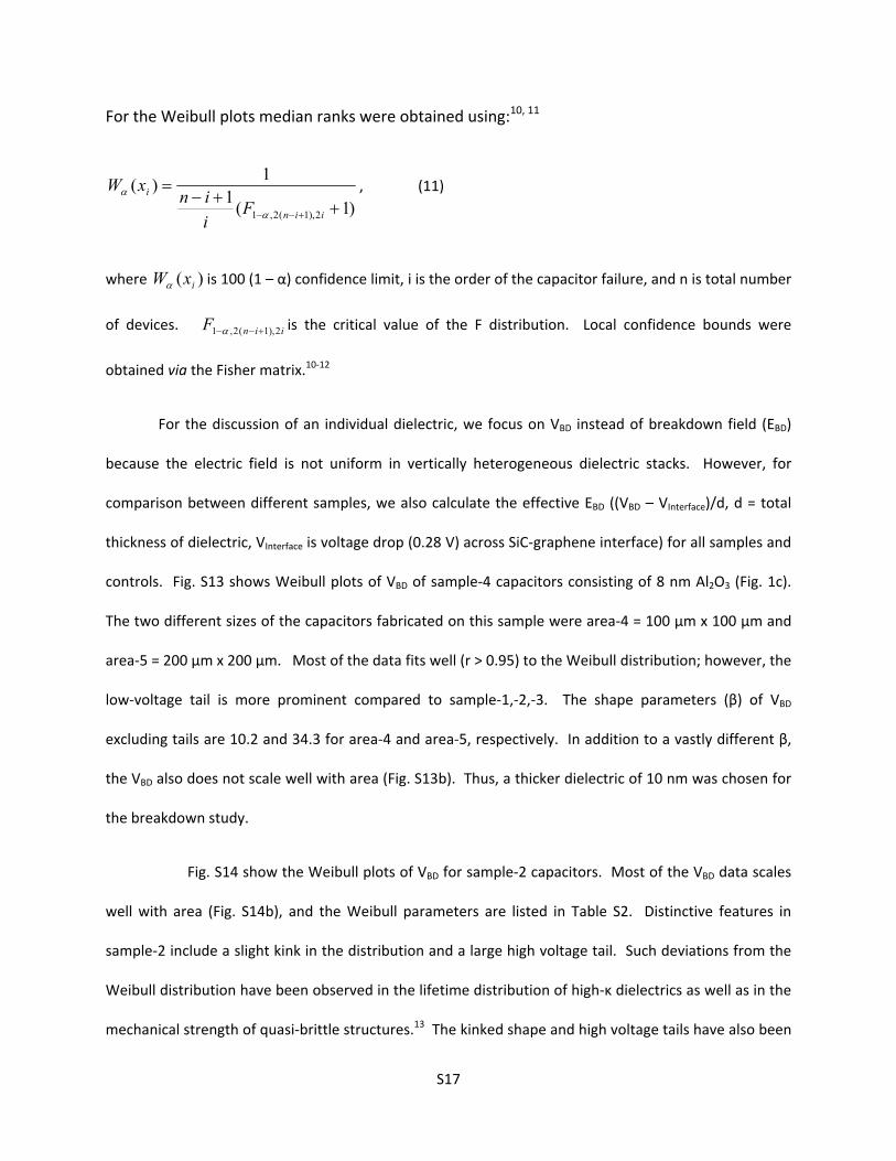
For the Weibull plots median ranks were obtained using:10, 11
)1(1
1)(
2),1(2,1
iin
i
Fi
inxW
, (11)
where )( ixW is 100 (1 – α) confidence limit, i is the order of the capacitor failure, and n is total number
of devices. iinF 2),1(2,1 is the critical value of the F distribution. Local confidence bounds were
obtained via the Fisher matrix.10‐12
For the discussion of an individual dielectric, we focus on VBD instead of breakdown field (EBD)
because the electric field is not uniform in vertically heterogeneous dielectric stacks. However, for
comparison between different samples, we also calculate the effective EBD ((VBD – VInterface)/d, d = total
thickness of dielectric, VInterface is voltage drop (0.28 V) across SiC‐graphene interface) for all samples and
controls. Fig. S13 shows Weibull plots of VBD of sample‐4 capacitors consisting of 8 nm Al2O3 (Fig. 1c).
The two different sizes of the capacitors fabricated on this sample were area‐4 = 100 µm x 100 µm and
area‐5 = 200 µm x 200 µm. Most of the data fits well (r > 0.95) to the Weibull distribution; however, the
low‐voltage tail is more prominent compared to sample‐1,‐2,‐3. The shape parameters (β) of VBD
excluding tails are 10.2 and 34.3 for area‐4 and area‐5, respectively. In addition to a vastly different β,
the VBD also does not scale well with area (Fig. S13b). Thus, a thicker dielectric of 10 nm was chosen for
the breakdown study.
Fig. S14 show the Weibull plots of VBD for sample‐2 capacitors. Most of the VBD data scales
well with area (Fig. S14b), and the Weibull parameters are listed in Table S2. Distinctive features in
sample‐2 include a slight kink in the distribution and a large high voltage tail. Such deviations from the
Weibull distribution have been observed in the lifetime distribution of high‐κ dielectrics as well as in the
mechanical strength of quasi‐brittle structures.13 The kinked shape and high voltage tails have also been

S18
accurately modeled by a probabilistic theory.13 High voltage tails are less relevant from a reliability
perspective since they have been hypothesized to originate from a different breakdown mechanism
dominating at higher voltages. Note that high voltage tails were also previously reported in the
breakdown analysis of solution‐processed ultra‐thin organic‐inorganic hybrid dielectrics.10, 11
Fig. S15 shows Weibull plots of the VBD distribution for sample‐3 capacitors. HfO2 directly grown
on PTCDA was found to be mechanically fragile. The dielectric layer peeled‐off during accidental direct
contact with the probes and thus contamination made the subsequent probe contacts non‐conducting.
Therefore, there is only limited VBD data for the smallest devices (area‐1) where direct contact between
probe and oxide was more frequent than the larger area devices. VBD data of sample‐3 did not show any
low‐voltage or high‐voltage tails; however, occurrences of “leaky capacitors” was higher than both
sample‐1 and sample‐2 (Table S2). In addition, the shape parameter (β) was found to be lower than
both sample‐1 and sample‐2. The VBD data scale well with area (Fig. S15b), and the extracted Weilbull
parameters are listed in Table S2.
Fig. S16 shows Weibull plots of the VBD distribution for control‐1 on a Si substrate. The absence
of any “leaky capacitors” and low voltage tails suggests high quality of ALD growth on the Si substrate, as
expected. The majority of the data excluding high voltage tails scales well with area (Fig. S16b). The
shape parameter (β) of the distribution was found to be more than 150; however, we note that this
number may be overestimated due to an artifact of infinite slope in the cumulative distribution of data
containing identical VBD values due to finite ramp rate step (0.01 V).

S19
Figure S13. (a) Weibull plot of VBD for capacitors of two sizes on the sample‐4 substrate. The dashed
lines show 95 % confidence bounds. (b) Area‐scaled Weibull plot of VBD for sample‐4.
Figure S14. (a) Weibull plot of VBD for capacitors of three sizes on the sample‐2 substrate. The dashed
lines show 95 % confidence bounds. (b) Area‐scaled Weibull plot of VBD for sample‐2.

S20
Figure S15. (a) Weibull plot of VBD for capacitors of three sizes on the sample‐3 substrate. The dashed
lines show 95 % confidence bounds. (b) Area‐scaled Weibull plot of VBD for sample‐3.
Figure S16. (a) Weibull plot of VBD for devices of two sizes on the control‐1 substrate. The dashed lines
show 95 % confidence bounds. (b) Area‐scaled Weibull plot of VBD for control‐1.
S21
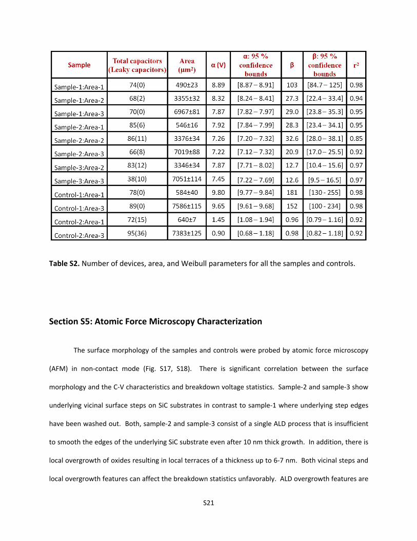
Table S2. Number of devices, area, and Weibull parameters for all the samples and controls.
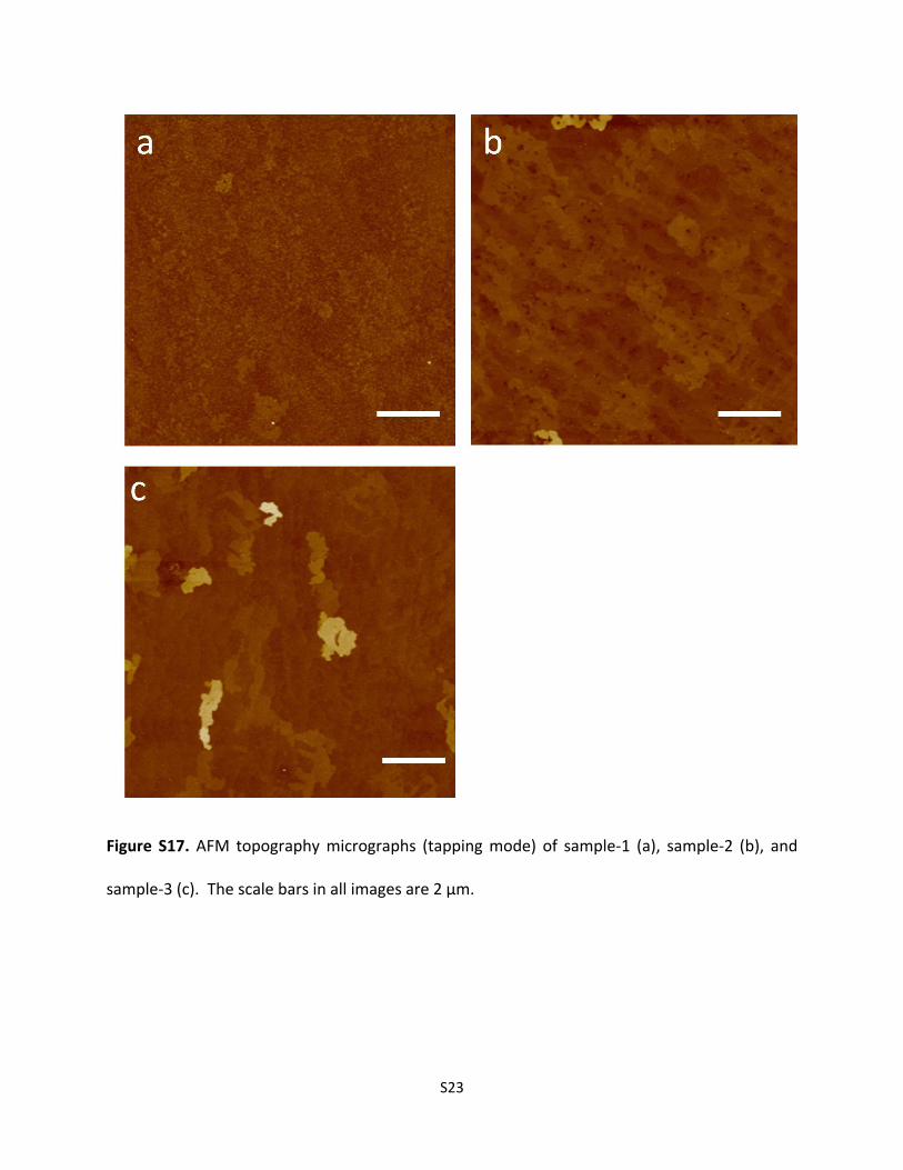
Section S5: Atomic Force Microscopy Characterization
The surface morphology of the samples and controls were probed by atomic force microscopy
(AFM) in non‐contact mode (Fig. S17, S18). There is significant correlation between the surface
morphology and the C‐V characteristics and breakdown voltage statistics. Sample‐2 and sample‐3 show
underlying vicinal surface steps on SiC substrates in contrast to sample‐1 where underlying step edges
have been washed out. Both, sample‐2 and sample‐3 consist of a single ALD process that is insufficient
to smooth the edges of the underlying SiC substrate even after 10 nm thick growth. In addition, there is
local overgrowth of oxides resulting in local terraces of a thickness up to 6‐7 nm. Both vicinal steps and
local overgrowth features can affect the breakdown statistics unfavorably. ALD overgrowth features are
S22
more frequent in the case of sample‐3 compared to sample‐2, resulting in a larger variation in the
capacitance in sample‐3. In contrast, two subsequent ALD processes on sample‐1 effectively wash‐out
the underlying vicinal steps of the SiC substrate. In addition, local overgrowth features were found to be
extremely rare. Therefore, multiple ALD processes can also help in minimizing the density of pin‐holes
throughout the oxide stack. Overall, the surface morphology provides direct evidence that supports the
experimental observation of a larger number of “leaky capacitors” and smaller Weibull scale parameter
(α) and shape parameter (β) in sample‐2 and sample‐3 compared to sample‐1. Note that surface
roughness of the dielectric within a single terrace on SiC is comparable for sample‐1, sample‐2, and
sample‐3 (rms roughness of 0.8 – 1.1 nm).
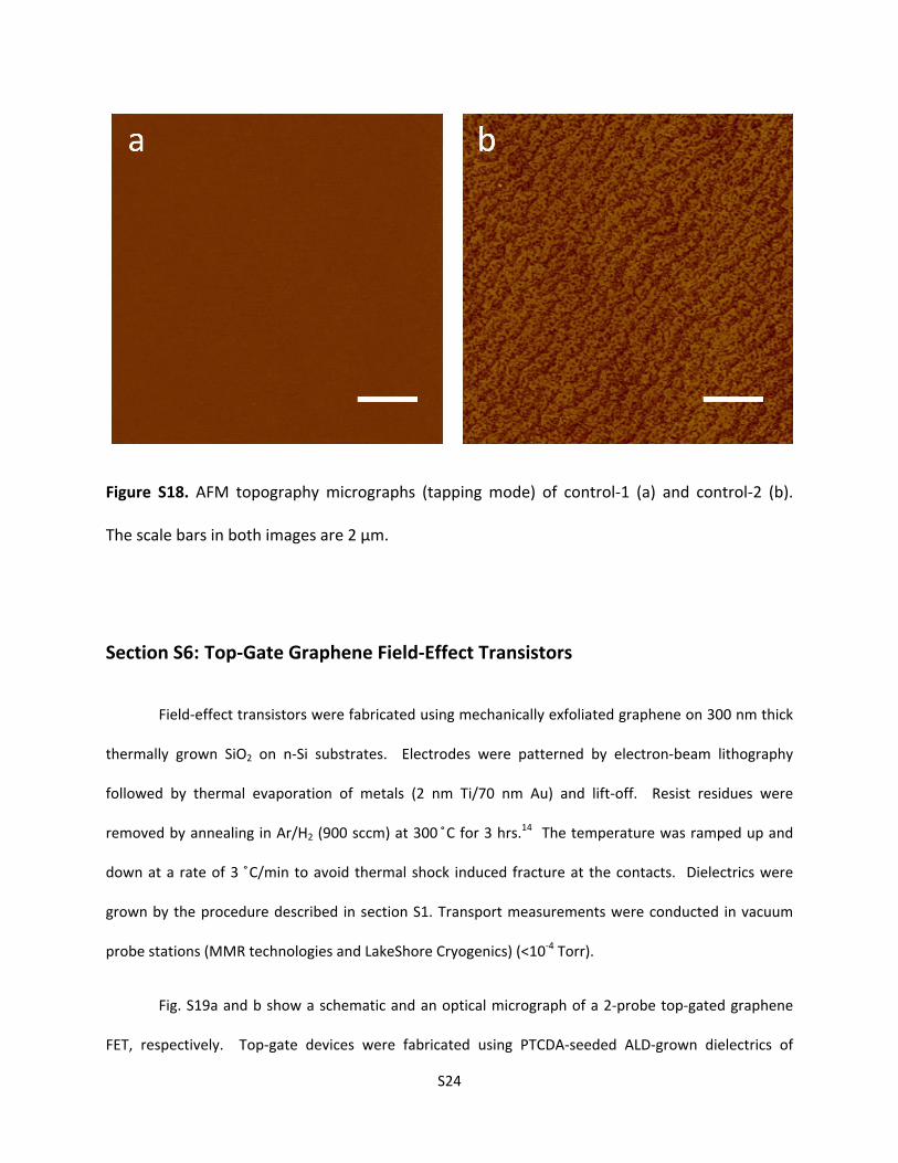
AFM images of control‐1 (Fig. S18a) show an ultra‐smooth surface with rms roughness of 0.25
nm, which is consistent with the absence of any “leaky capacitors” and high reliability and breakdown
strength of control‐1. In contrast, AFM images of control‐2 (Fig. S18b) show not only vicinal steps from
the underlying SiC substrate but also highly rugged oxide growth even within a single terrace, resulting
in rms roughness of 1.8 nm.
S23
Figure S17. AFM topography micrographs (tapping mode) of sample‐1 (a), sample‐2 (b), and
sample‐3 (c). The scale bars in all images are 2 µm.
S24
Figure S18. AFM topography micrographs (tapping mode) of control‐1 (a) and control‐2 (b).
The scale bars in both images are 2 µm.
Section S6: Top‐Gate Graphene Field‐Effect Transistors
Field‐effect transistors were fabricated using mechanically exfoliated graphene on 300 nm thick
thermally grown SiO2 on n‐Si substrates. Electrodes were patterned by electron‐beam lithography
followed by thermal evaporation of metals (2 nm Ti/70 nm Au) and lift‐off. Resist residues were
removed by annealing in Ar/H2 (900 sccm) at 300 ̊C for 3 hrs.14 The temperature was ramped up and
down at a rate of 3 ̊C/min to avoid thermal shock induced fracture at the contacts. Dielectrics were
grown by the procedure described in section S1. Transport measurements were conducted in vacuum
probe stations (MMR technologies and LakeShore Cryogenics) (<10‐4 Torr).
Fig. S19a and b show a schematic and an optical micrograph of a 2‐probe top‐gated graphene
FET, respectively. Top‐gate devices were fabricated using PTCDA‐seeded ALD‐grown dielectrics of

S25
multiple thicknesses: 20 nm Al2O3, 10 nm Al2O3, 4 nm Al2O3 and 2 nm Al2O3/8 nm HfO2. For transport
measurements, a constant drain current of 1 µA was applied, and the drain voltage was measured as a
function of top‐electrode voltage (Vtg) by a lock‐in amplifier while keeping the bottom gate grounded.
Total resistance (Rtotal) versus Vtg characteristics of a device with 4 nm Al2O3 dielectric device is shown in
Fig. S19c. Intrinsic field‐effect mobility (µ) is calculated by fitting the transfer curve with the following
equation:15
22
/
TGo
ctotal
nne
WLRR
, (12)
where Rtotal is total resistance of the device, Rc is the combined resistance of the contacts and the
exposed part of the graphene in the channel, e is electronic charge, n0 is residual carrier concentration,
nTG is carrier density induced by the top‐gate bias, L is top‐gate length, and W is channel width. For low
capacitance gate dielectrics, nTG can be obtained from:
e
VVCn DiracTGTGTG
)( , (13)
where VTG is the top‐gate voltage, VDirac is the charge neutrality point, and cTG is the top‐gate
capacitance. However, in cases of high capacitance dielectrics, the quantum capacitance of graphene
should also be considered to calculate the carrier density. Therefore, the calculation of mobility is
accomplished by obtaining an expression for nTG from the following equation (also see equations 1‐5):
e
n
C
enVV TGF
TG
TGDiracTG
, (14)
where is Planck’s constant divided by 2π, and νF is Fermi velocity of graphene (106 m/s).
The fitting
parameters are Rc, n0, and µ. The extracted field‐effect mobilities of all the measured devices range
S26
between 2000 – 3500 cm2/Vs. The mobility of the 4 nm Al2O3 device was found to be 2405 cm2/Vs
without including quantum capacitance and 3252 cm2/Vs using the quantum capacitance correction (Fig.
S19c). The mobility of these FETs is expected to improve by stricter cleaning protocols and higher
quality graphene flakes. A more relevant parameter for high frequency devices is the transconductance
(gm) defined as TG
m Vg
, where σ is the conductivity of the channel. However, since
transconductance depends on the size of the channel, a more intrinsic transconductance parameter
(gnormalized) defined as TGmnormalized CW
Lgg . should be compared with the literature.16 The highest
gnormalized for 4 nm Al2O3 FET was found to be 3.2 mS, which is among the highest values achieved for
graphene (for example, gnormalized for 155 GHz transistors ~ 1 mS (IBM)17, gnormalized for Y2O3 dielectric ~ 7.9
mS (Peking University)16, gnormalized ~ 4.7 mS (Manchester)18, gnormalized ~ 3.8 mS (UCLA)19 ).

S27
Figure S19. (a) Schematic of a top‐gated graphene FET on an SiO2/Si substrate. (b) Optical micrograph of
a 2‐probe graphene FET with 4 nm Al2O3 top‐gate dielectric with a channel length of 9 µm, top‐gate
length of 8 µm, and channel width of 3 µm. (c) Transfer curve of the GFET‐4 device with bottom
electrode grounded. The red line is a model fit to the data (black circles).
S28
References:
1. Johns, J. E.; Karmel, H. J.; Alaboson, J. M. P.; Hersam, M. C. J. Phys. Chem. Lett. 2012, 3, 1974. 2. Alaboson, J. M. P.; Wang, Q. H.; Emery, J. D.; Lipson, A. L.; Bedzyk, M. J.; Elam, J. W.; Pellin, M. J.; Hersam, M. C. ACS Nano 2011, 5, 5223. 3. Ni, Z. H.; Chen, W.; Fan, X. F.; Kuo, J. L.; Yu, T.; Wee, A. T. S.; Shen, Z. X. Phys. Rev. B 2008, 77, 115416. 4. Xia, J.; Chen, F.; Li, J.; Tao, N. Nat. Nanotech. 2009, 4, 505. 5. Fang, T.; Konar, A.; Xing, H.; Jena, D. Appl. Phys. Lett. 2007, 91, 092109. 6. DiBenedetto, S. A.; Facchetti, A.; Ratner, M. A.; Marks, T. J. Journal of the American Chemical Society 2009, 131, 7158. 7. Groner, M. D.; Elam, J. W.; Fabreguette, F. H.; George, S. M. Thin Solid Films 2002, 413, 186. 8. Cheong, K. Y.; Moon, J. H.; Kim, H. J.; Bahng, W.; Kim, N.‐K. J. Appl. Phys. 2008, 103, 084113. 9. Wu, Y. Q.; Lin, H. C.; Ye, P. D.; Wilk, G. D. Appl. Phys. Lett. 2007, 90, 072105. 10. Schlitz, R. A.; Ha, Y.‐g.; Marks, T. J.; Lauhon, L. J. ACS Nano 2012, 6, 4452. 11. Schlitz, R. A.; Yoon, K.; Fredin, L. A.; Ha, Y.‐g.; Ratner, M. A.; Marks, T. J.; Lauhon, L. J. J. Phys. Chem. Lett. 2010, 1, 3292. 12. Dodson, B., Weibull Analysis. ASQC Quality Press: Milwaukee, WI, 1994. 13. Le, J.‐L.; Bazant, Z. P.; Bazant, M. Z. J. Appl. Phys. 2009, 106, 104119. 14. Ishigami, M.; Chen, J. H.; Cullen, W. G.; Fuhrer, M. S.; Williams, E. D. Nano Lett. 2007, 7, 1643. 15. Kim, S.; Nah, J.; Jo, I.; Shahrjerdi, D.; Colombo, L.; Yao, Z.; Tutuc, E.; Banerjee, S. K. Appl. Phys. Lett. 2009, 94, 062107. 16. Xu, H.; Zhang, Z.; Xu, H.; Wang, Z.; Wang, S.; Peng, L.‐M. ACS Nano 2011, 5, 5031. 17. Wu, Y.; Lin, Y.‐m.; Bol, A. A.; Jenkins, K. A.; Xia, F.; Farmer, D. B.; Zhu, Y.; Avouris, P. Nature 2011, 472, 74. 18. Ponomarenko, L. A.; Yang, R.; Gorbachev, R. V.; Blake, P.; Mayorov, A. S.; Novoselov, K. S.; Katsnelson, M. I.; Geim, A. K. Phys. Rev. Lett. 2010, 105, 136801. 19. Liao, L.; Bai, J.; Qu, Y.; Lin, Y.‐c.; Li, Y.; Huang, Y.; Duan, X. Proc. Natl. Acad. Sci. U.S.A. 2010, 107, 6711.
Related Documents