Click to add presentation title Click to edit Master subtitle Click to add date Study On Two-stage Architecture For Synchronous Buck Converter In High-power-density Computing Power Supplies Tirthajyoti Sarkar, Bhargava C.V., Mona Joshi, Ritu Sodhi, Steve Sapp 11/14/2012 Presenter: Art Black, Fairchild Semiconductor

Welcome message from author
This document is posted to help you gain knowledge. Please leave a comment to let me know what you think about it! Share it to your friends and learn new things together.
Transcript

Click to addpresentation titleClick to edit Master subtitle
Click to add date
Study On Two-stage ArchitectureFor Synchronous Buck ConverterIn High-power-density ComputingPower Supplies
Tirthajyoti Sarkar, Bhargava C.V., Mona
Joshi, Ritu Sodhi, Steve Sapp
11/14/2012
Presenter: Art Black, Fairchild Semiconductor
2
Outline
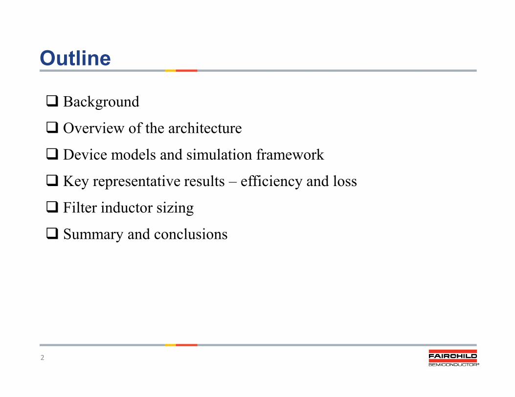
Background
Overview of the architecture
Device models and simulation framework
Key representative results – efficiency and loss
Filter inductor sizing
Summary and conclusions
3
Background Next-generation computing power supplies (for desktops, servers, and notebooks) aspire tohave higher power density. Higher switching frequency is an obviously attractive optiontowards that goal.
Synchronous buck converter, most widely used circuit topology for computing applications,faces some problems in this regard with respect to extremely narrow duty cycles on the high-side (HS) device compared to the low-side (LS) device. Further, their breakdown voltage rating isgoverned by the input voltage whereas the major loss comes from high conduction current ,governed by the output power and low output voltage.
Increased duty-cycle would be a potential solution this issue. Also, by decreasing the inputvoltage and using low-voltage-rating devices, efficiency and power density can be enhanced.However, because common voltage-regulator module (VRM) specifications fix the input andoutput voltage bounds, arbitrary choice of duty cycle or input voltage is not possible with theconventional single-stage topology. In this regard, a two-stage cascaded approach can be adopted.
In this study, we illustrate some results which may yield insights on (a) advantage of the two-stage approach with regard to increasing switching frequency of the stage delivering power tothe load, (b) distribution of loss between the two stages, (c) switching frequency partitionwhich separates the two-stage solution from conventional single-stage approach from power lossstandpoint, and (d) simplified power density comparison among different architectures based onfilter inductor size.
4
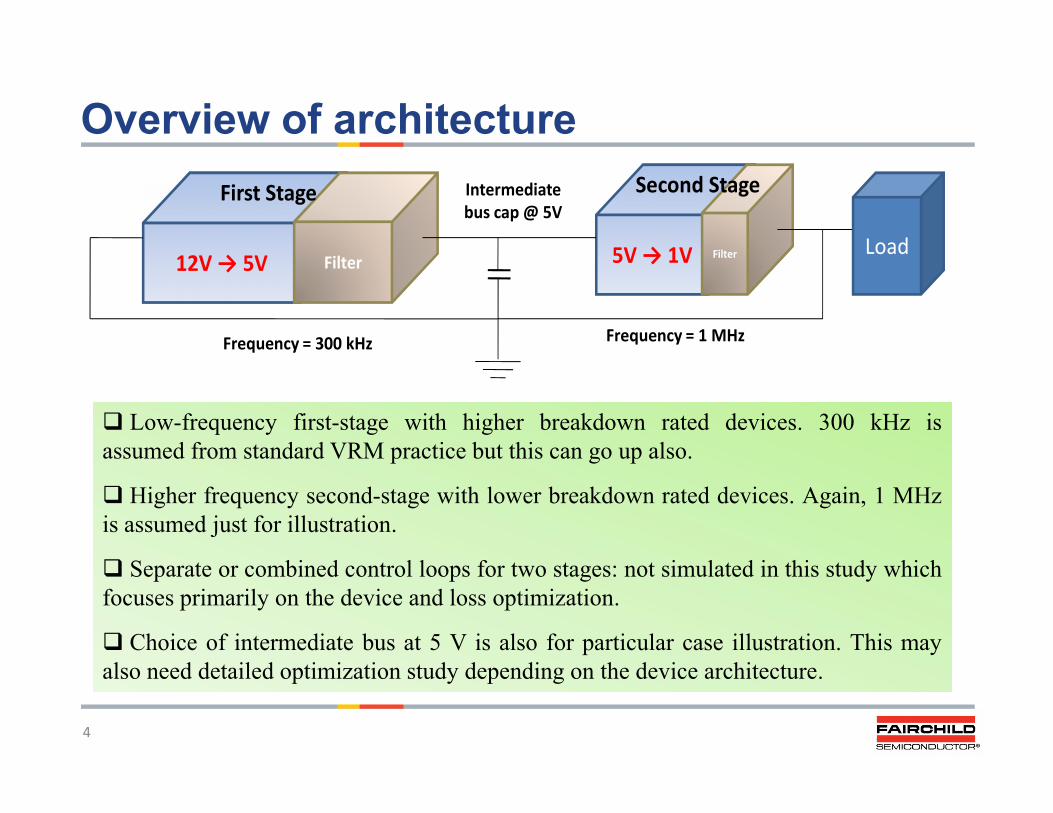
Overview of architecture
12V → 5V 5V → 1V
Intermediatebus cap @ 5V
Frequency = 300 kHz Frequency = 1 MHz
Filter Filter
First Stage Second Stage
Load
Low-frequency first-stage with higher breakdown rated devices. 300 kHz isassumed from standard VRM practice but this can go up also.
Higher frequency second-stage with lower breakdown rated devices. Again, 1 MHzis assumed just for illustration.
Separate or combined control loops for two stages: not simulated in this study whichfocuses primarily on the device and loss optimization.
Choice of intermediate bus at 5 V is also for particular case illustration. This mayalso need detailed optimization study depending on the device architecture.
5
Possible flavors – Case 1 and 2
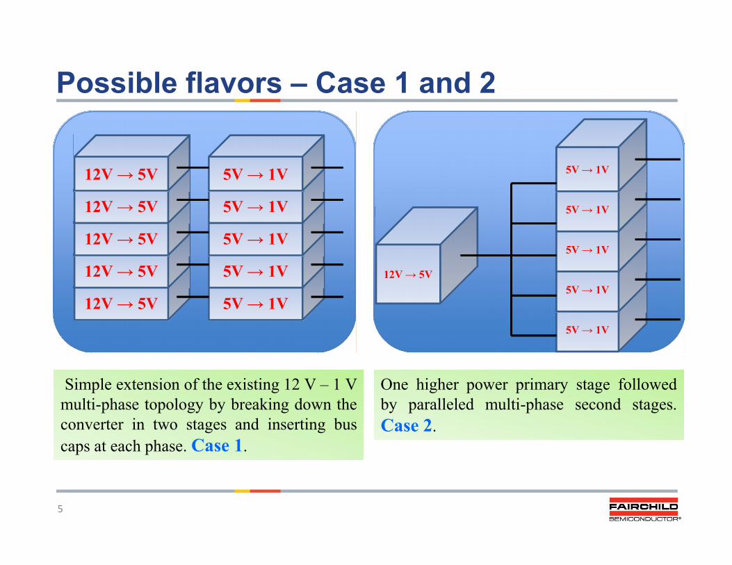
12V → 5V 5V → 1V
12V → 5V 5V → 1V
12V → 5V 5V → 1V
12V → 5V 5V → 1V
12V → 5V 5V → 1V
Simple extension of the existing 12 V – 1 Vmulti-phase topology by breaking down theconverter in two stages and inserting buscaps at each phase. Case 1.
12V → 5V
5V → 1V
5V → 1V
5V → 1V
5V → 1V
5V → 1V
One higher power primary stage followedby paralleled multi-phase second stages.Case 2.
6
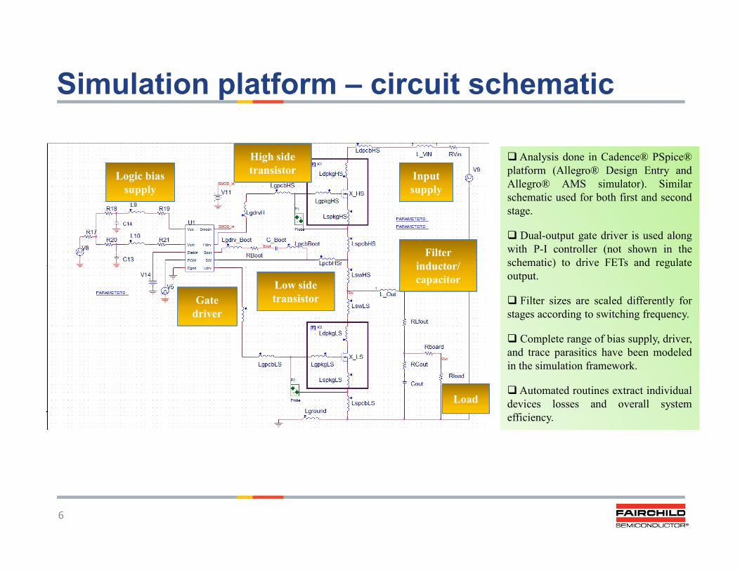
Simulation platform – circuit schematic
High sidetransistorHigh sidetransistor
Low sidetransistorLow sidetransistor
Filterinductor/capacitor
Filterinductor/capacitor
LoadLoad
Logic biassupply
Logic biassupply
GatedriverGate
driver
Analysis done in Cadence® PSpice®platform (Allegro® Design Entry andAllegro® AMS simulator). Similarschematic used for both first and secondstage.
Dual-output gate driver is used alongwith P-I controller (not shown in theschematic) to drive FETs and regulateoutput.
Filter sizes are scaled differently forstages according to switching frequency.
Complete range of bias supply, driver,and trace parasitics have been modeledin the simulation framework.
Automated routines extract individualdevices losses and overall systemefficiency.
InputsupplyInputsupply
7
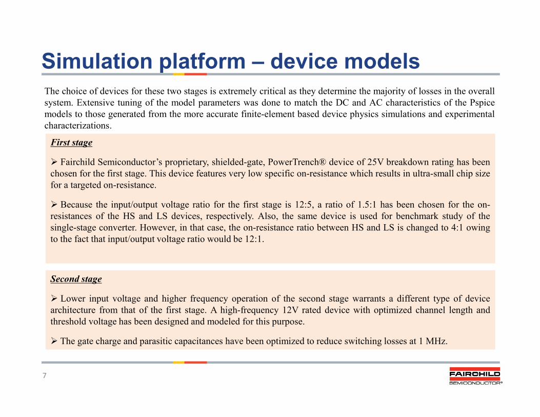
Simulation platform – device modelsThe choice of devices for these two stages is extremely critical as they determine the majority of losses in the overallsystem. Extensive tuning of the model parameters was done to match the DC and AC characteristics of the Pspicemodels to those generated from the more accurate finite-element based device physics simulations and experimentalcharacterizations.
Second stage
Lower input voltage and higher frequency operation of the second stage warrants a different type of devicearchitecture from that of the first stage. A high-frequency 12V rated device with optimized channel length andthreshold voltage has been designed and modeled for this purpose.
The gate charge and parasitic capacitances have been optimized to reduce switching losses at 1 MHz.
First stage
Fairchild Semiconductor’s proprietary, shielded-gate, PowerTrench® device of 25V breakdown rating has beenchosen for the first stage. This device features very low specific on-resistance which results in ultra-small chip sizefor a targeted on-resistance.
Because the input/output voltage ratio for the first stage is 12:5, a ratio of 1.5:1 has been chosen for the on-resistances of the HS and LS devices, respectively. Also, the same device is used for benchmark study of thesingle-stage converter. However, in that case, the on-resistance ratio between HS and LS is changed to 4:1 owingto the fact that input/output voltage ratio would be 12:1.
8
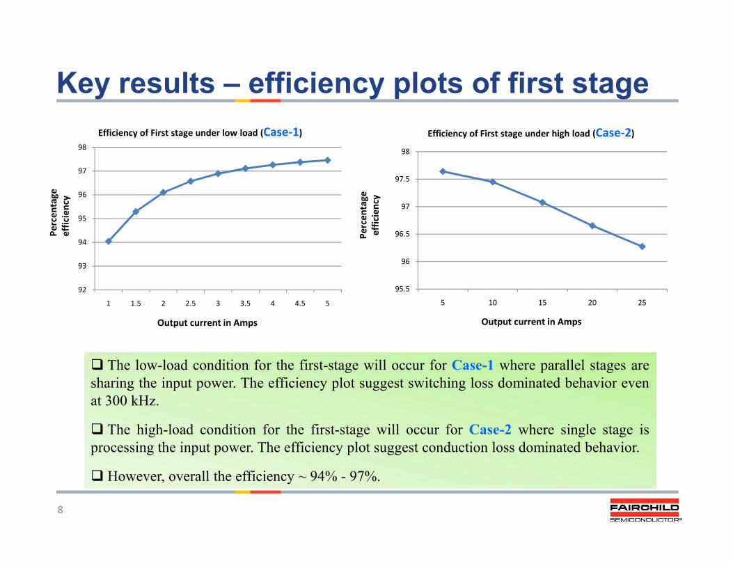
Key results – efficiency plots of first stage
92
93
94
95
96
97
98
1 1.5 2 2.5 3 3.5 4 4.5 5
Efficiency of First stage under low load (Case-1)
Output current in Amps
Perc
enta
geef
ficie
ncy
95.5
96
96.5
97
97.5
98
5 10 15 20 25
Efficiency of First stage under high load (Case-2)
Output current in Amps
Perc
enta
geef
ficie
ncy
The low-load condition for the first-stage will occur for Case-1 where parallel stages aresharing the input power. The efficiency plot suggest switching loss dominated behavior evenat 300 kHz.
The high-load condition for the first-stage will occur for Case-2 where single stage isprocessing the input power. The efficiency plot suggest conduction loss dominated behavior.
However, overall the efficiency ~ 94% - 97%.
9
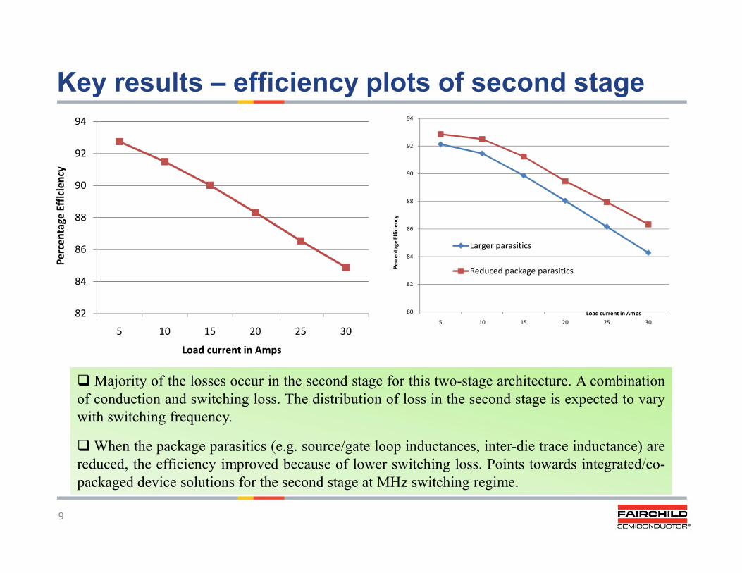
Key results – efficiency plots of second stage
82
84
86
88
90
92
94
5 10 15 20 25 30
Load current in Amps
Perc
enta
ge E
ffici
ency
80
82
84
86
88
90
92
94
5 10 15 20 25 30
Larger parasitics
Reduced package parasitics
Load current in Amps
Perc
enta
ge E
ffici
ency
Majority of the losses occur in the second stage for this two-stage architecture. A combinationof conduction and switching loss. The distribution of loss in the second stage is expected to varywith switching frequency.
When the package parasitics (e.g. source/gate loop inductances, inter-die trace inductance) arereduced, the efficiency improved because of lower switching loss. Points towards integrated/co-packaged device solutions for the second stage at MHz switching regime.
10
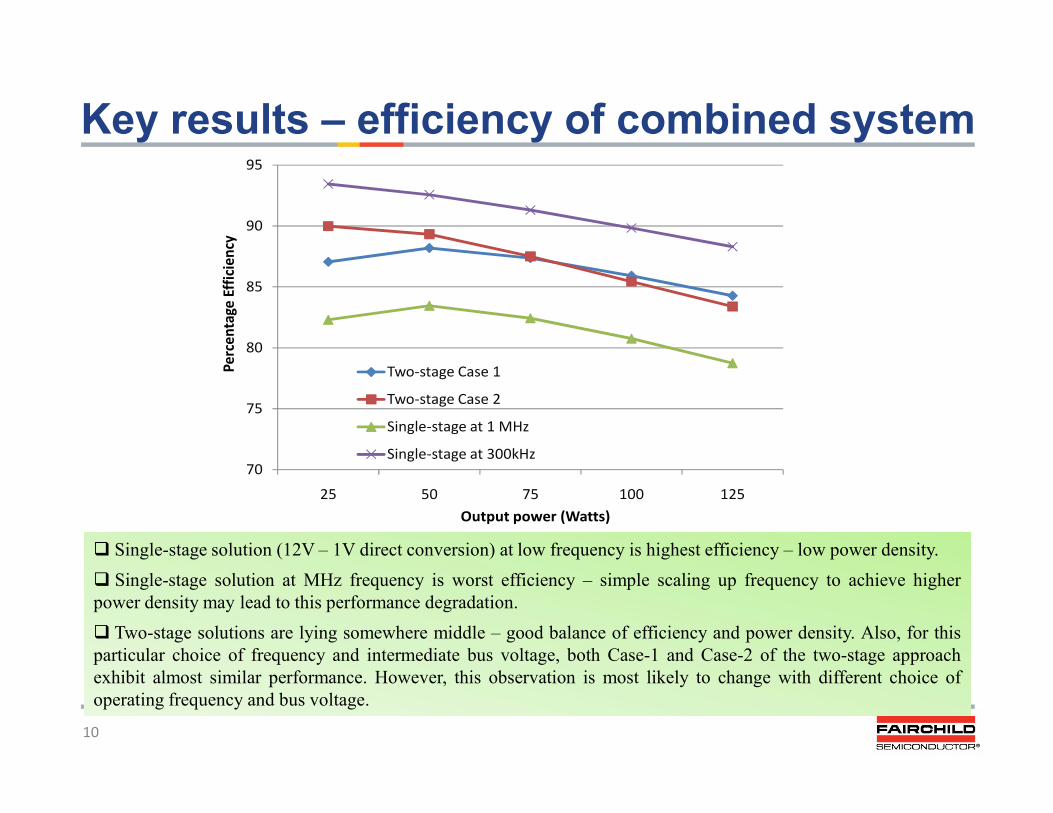
Key results – efficiency of combined system
70
75
80
85
90
95
25 50 75 100 125
Two-stage Case 1
Two-stage Case 2
Single-stage at 1 MHz
Single-stage at 300kHz
Output power (Watts)
Perc
enta
ge E
ffici
ency
Single-stage solution (12V – 1V direct conversion) at low frequency is highest efficiency – low power density. Single-stage solution at MHz frequency is worst efficiency – simple scaling up frequency to achieve higherpower density may lead to this performance degradation. Two-stage solutions are lying somewhere middle – good balance of efficiency and power density. Also, for thisparticular choice of frequency and intermediate bus voltage, both Case-1 and Case-2 of the two-stage approachexhibit almost similar performance. However, this observation is most likely to change with different choice ofoperating frequency and bus voltage.
11
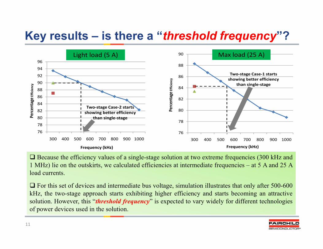
Key results – is there a “threshold frequency”?
7678808284868890929496
300 400 500 600 700 800 900 1000
Frequency (kHz)
Perc
enta
geEf
ficie
ncy
Two-stage Case-2 startsshowing better efficiency
than single-stage
Light load (5 A)
Perc
enta
geEf
ficie
ncy
76
78
80
82
84
86
88
90
300 400 500 600 700 800 900 1000
Two-stage Case-1 startsshowing better efficiency
than single-stage
Max load (25 A)
Frequency (kHz)
Because the efficiency values of a single-stage solution at two extreme frequencies (300 kHz and1 MHz) lie on the outskirts, we calculated efficiencies at intermediate frequencies – at 5 A and 25 Aload currents.
For this set of devices and intermediate bus voltage, simulation illustrates that only after 500-600kHz, the two-stage approach starts exhibiting higher efficiency and starts becoming an attractivesolution. However, this “threshold frequency” is expected to vary widely for different technologiesof power devices used in the solution.
12
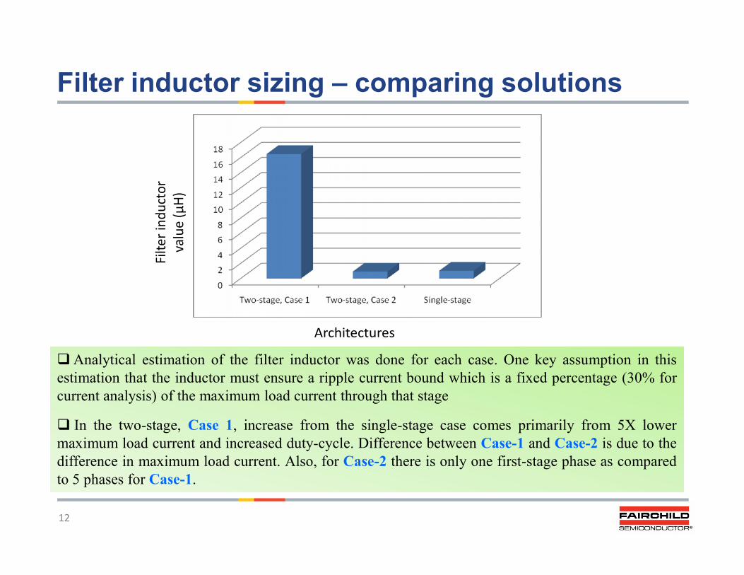
Filter inductor sizing – comparing solutions
Filte
rind
ucto
rva
lue
(µH)
Architectures
Analytical estimation of the filter inductor was done for each case. One key assumption in thisestimation that the inductor must ensure a ripple current bound which is a fixed percentage (30% forcurrent analysis) of the maximum load current through that stage
In the two-stage, Case 1, increase from the single-stage case comes primarily from 5X lowermaximum load current and increased duty-cycle. Difference between Case-1 and Case-2 is due to thedifference in maximum load current. Also, for Case-2 there is only one first-stage phase as comparedto 5 phases for Case-1.
13
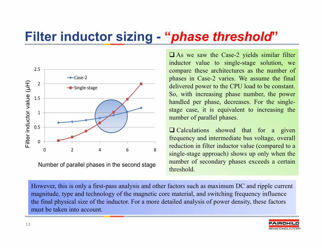
Filter inductor sizing - “phase threshold”
Number of parallel phases in the second stage
Filt
erin
duct
or v
alue
(µH
)
0
0.5
1
1.5
2
2.5
0 2 4 6 8
Case-2
Single-stage
As we saw the Case-2 yields similar filterinductor value to single-stage solution, wecompare these architectures as the number ofphases in Case-2 varies. We assume the finaldelivered power to the CPU load to be constant.So, with increasing phase number, the powerhandled per phase, decreases. For the single-stage case, it is equivalent to increasing thenumber of parallel phases.
Calculations showed that for a givenfrequency and intermediate bus voltage, overallreduction in filter inductor value (compared to asingle-stage approach) shows up only when thenumber of secondary phases exceeds a certainthreshold.
However, this is only a first-pass analysis and other factors such as maximum DC and ripple currentmagnitude, type and technology of the magnetic core material, and switching frequency influencethe final physical size of the inductor. For a more detailed analysis of power density, these factorsmust be taken into account.
14
Summary and Conclusions Two-stage architecture may help in pushing the operating frequency in the MHz range of thefinal stage which will deliver power into the microprocessor, without degrading the efficiency asseverely as in the case of single-stage architecture. However, advantage of two-stage over asingle-stage topology starts showing up only above a certain frequency threshold.
Major loss in the two-stage architecture concentrates around the high-frequency, high-currentsecond stage which needs maximum emphasis from device and circuit optimization point ofview. However, this stage contributes far less volume (from filter standpoint) as compared to thefirst stage.
While adopting two-stage architecture, a simple parallelization of the single-stage architecturemay not be beneficial from power density point of view. A single high-power first-stage followedby multiple parallel-connected second-stages may be the preferred architecture from thestandpoint of filter inductor value. However, actual physical size of the inductor may depend uponother factors and the technology and type of the magnetic core material.
Further, the power density benefit may show up only after the number of parallel secondarystages exceeds a certain threshold. But increasing the parallel phases may affect the powerconversion efficiency. Therefore, the power density optimization must be coupled with overallloss estimation for a better system design.
15
Extension possibilities…
Intermediate bus voltage may have an optimized value for a given choice ofdevice technology. This study assumed one fixed voltage, but the choice is wideopen…
Non-traditional structures for the second stage high-frequency power device– LDMOS? Advanced material? Fully integrated MOSFET and gate driver?
Choice of switching frequencies on the two stages may be separatelyoptimized depending on the device technology and level of integration.
Filter technology for the high-frequency stage need to be carefully selected(high-density thin-film/integrated magnetics? Can these technologies cope withhigh current density?). Thereafter, coupled analysis of power density and losswill lead to better system optimization.

16
Thank You!!
For questions and clarifications please contact Tirthajyoti Sarkar [email protected].
Related Documents