Materials Science in Semiconductor Processing 9 (2006) 1049–1054 Structure analysis of the system Hafnium/Siliconð100Þ by means of X-ray photoelectron spectroscopy and X-ray photoelectron diffraction (XPD) C.R. Flu¨chter a,b, , A. de Siervo c , D. Weier a,b , M. Schu¨rmann a , U. Berges a,b , S. Dreiner a , M.F. Carazzolle d , R. Landers c,d , G.G. Kleiman d , C. Westphal a,b a Experimentelle Physik 1, Universita ¨ t Dortmund, Otto-Hahn-Str.4, D 44221 Dortmund, Germany b DELTA, Universita ¨ t Dortmund, Maria-Goeppert-Mayer-Str. 2, D 44227 Dortmund, Germany c Laborato ´rio Nacional de Luz Sı´ncrotron, C.P. 6192, 13084-971 Campinas, SP, Brazil d Instituto de Fisica, Universidade Estadual de Campinas, C.P. 6165, 13083-970 Campinas, SP, Brazil Available online 7 November 2006 Abstract Due to the ongoing miniaturization of semiconductor devices new gate dielectrics are required for future applications. In this work we investigated hafnium silicide as a pre-system for hafnium oxide, one of the most promising candidates. One of the major problems of HfO 2 -films on silicon is the formation of hafnium silicide at the HfO 2 =Si interface. Therefore, ultrathin films of the system HfSi on Sið100Þ with a systematic varied thickness from 3 to 30 A ˚ were prepared. Measurements were conducted by means of X-ray photoelectron spectroscopy and low energy electron diffraction (LEED). Also full 2p X-ray photoelectron diffraction (XPD) patterns with high spectral resolution were recorded. Against other reports related to thicker films, several heating cycles showed no phase transitions of the ultrathin films. However, above temperatures of 630 C an island formation is strongly indicated. The experimental XPD patterns are compared to simulated patterns of model structures. For the first time we present a modification of the C49 structure a possible structure for ultrathin HfSi 2 -films on bulk Si. As an outlook possibilities for preparing the system HfO 2 =Sið100Þ are introduced. r 2006 Elsevier Ltd. All rights reserved. Keywords: Photoelectron diffraction; Photoelectron spectroscopy; Silicon; High-k 1. Introduction In the past years, the search for new gate dielectrics used in integrated circuits became more and more demanding. Silicon dioxide that has been used for decades will become inefficient with the ongoing miniaturization of these devices. This is caused by increasing tunneling currents for a decreased insulating layer thickness. Below an estimated SiO 2 -film thickness of around 15 A ˚ no further gain in the performance of a MOSFET (metal oxide semiconductor field effect transistor) is expected [1]. Besides the layer thickness of the film, the dielectric constant or k-value of the insulating ARTICLE IN PRESS 1369-8001/$ - see front matter r 2006 Elsevier Ltd. All rights reserved. doi:10.1016/j.mssp.2006.10.022 Corresponding author. E-mail address: christian.fl[email protected] (C.R. Flu¨chter).

Welcome message from author
This document is posted to help you gain knowledge. Please leave a comment to let me know what you think about it! Share it to your friends and learn new things together.
Transcript
ARTICLE IN PRESS
1369-8001/$ - se
doi:10.1016/j.m
�CorrespondE-mail addr
(C.R. Fluchter)
Materials Science in Semiconductor Processing 9 (2006) 1049–1054
Structure analysis of the system Hafnium/Siliconð1 0 0Þby means of X-ray photoelectron spectroscopy and X-ray
photoelectron diffraction (XPD)
C.R. Fluchtera,b,�, A. de Siervoc, D. Weiera,b, M. Schurmanna, U. Bergesa,b,S. Dreinera, M.F. Carazzolled, R. Landersc,d, G.G. Kleimand, C. Westphala,b
aExperimentelle Physik 1, Universitat Dortmund, Otto-Hahn-Str.4, D 44221 Dortmund, GermanybDELTA, Universitat Dortmund, Maria-Goeppert-Mayer-Str. 2, D 44227 Dortmund, Germany
cLaboratorio Nacional de Luz Sıncrotron, C.P. 6192, 13084-971 Campinas, SP, BrazildInstituto de Fisica, Universidade Estadual de Campinas, C.P. 6165, 13083-970 Campinas, SP, Brazil
Available online 7 November 2006
Abstract
Due to the ongoing miniaturization of semiconductor devices new gate dielectrics are required for future applications. In
this work we investigated hafnium silicide as a pre-system for hafnium oxide, one of the most promising candidates. One of
the major problems of HfO2-films on silicon is the formation of hafnium silicide at the HfO2=Si interface. Therefore,ultrathin films of the system HfSi on Sið1 0 0Þ with a systematic varied thickness from 3 to 30 A were prepared.
Measurements were conducted by means of X-ray photoelectron spectroscopy and low energy electron diffraction
(LEED). Also full 2p X-ray photoelectron diffraction (XPD) patterns with high spectral resolution were recorded. Against
other reports related to thicker films, several heating cycles showed no phase transitions of the ultrathin films. However,
above temperatures of 630 �C an island formation is strongly indicated. The experimental XPD patterns are compared to
simulated patterns of model structures. For the first time we present a modification of the C49 structure a possible
structure for ultrathin HfSi2-films on bulk Si. As an outlook possibilities for preparing the system HfO2=Sið1 0 0Þare introduced.
r 2006 Elsevier Ltd. All rights reserved.
Keywords: Photoelectron diffraction; Photoelectron spectroscopy; Silicon; High-k
1. Introduction
In the past years, the search for new gatedielectrics used in integrated circuits became moreand more demanding. Silicon dioxide that has been
e front matter r 2006 Elsevier Ltd. All rights reserved
ssp.2006.10.022
ing author.
ess: [email protected]
.
used for decades will become inefficient with theongoing miniaturization of these devices. This iscaused by increasing tunneling currents for adecreased insulating layer thickness. Below anestimated SiO2-film thickness of around 15 A nofurther gain in the performance of a MOSFET(metal oxide semiconductor field effect transistor) isexpected [1]. Besides the layer thickness of the film,the dielectric constant or k-value of the insulating
.
ARTICLE IN PRESSC.R. Fluchter et al. / Materials Science in Semiconductor Processing 9 (2006) 1049–10541050
layer is significant for the performance of anintegrated circuit device. Therefore, it was proposedrecently [2] to use thick layers of a material with amuch higher dielectric constant than SiO2 in orderto reduce tunneling effects by several orders ofmagnitude without debasing the devices efficiency.As substitutes for silicon dioxide several materialsare under investigation. Herein the oxides ofhafnium and zirconium are the most promisingcandidates as they offer a good tradeoff betweenk-value, band gap and band offset to silicon.
A major concern for future applications is thestructure of the interface of the gate dielectrics tothe bulk silicon. Either SiO2 or HfSi2 formationwould severely deteriorate the dielectric propertiesof the layer.
In this work, we report on an investigation on thesystem HfSi2=Sið1 0 0Þ as a pre-system to determinethe structure of hafnium on silicon and of ultrathinHfSi2 layers. Further first results on the systemHfO2=Sið1 0 0Þ are presented. For this, soft X-raysfrom the synchrotron radiation source DELTAwere used.
2. Experiment
All experiments and preparations were carriedout in a UHV chamber with a base pressure of5� 10�11 mbar. The system was investigated bymeans of X-ray photoelectron spectroscopy (XPS)and low energy electron diffraction (LEED). X-rayphotoelectron diffraction (XPD) patterns wererecorded and compared to computer simulationsin order to solve the structure of the system.
For standard film characterization procedures amagnesium X-ray tube ðhn ¼ 1253:6 eVÞ was used asan excitation source. Synchrotron light in the softX-ray regime ðhn ¼ 180 eVÞ was applied in order toenhance the surface sensitivity for low hafniumcoverage and to obtain high spectral resolution [3].Those experiments were conducted at the synchro-tron radiation source DELTA (beamlines 5 and 11,University of Dortmund).
Rectangular shaped samples of 6� 8mm sizewere cut out from a p-doped Sið1 0 0Þ-wafer. Afterdegassing the samples at a temperature of around700 �C for several hours the native oxide layer wasremoved by flash heating the sample at 1050 �C.After stepwise cooling, the samples showed a ð2� 1Þsurface reconstruction with two domains, aschecked by LEED. The hafnium was evaporatedonto the sample by an electron beam evaporator.
During the evaporation time of 0.5–5 h the pressurewas kept below �2� 10�10 mbar. By this, filmthicknesses of 3–30 A were achieved. The thicknesseswere calculated from the silicon photoelectron signalincluding the inelastically damping of the initiallyamorphous hafnium film [4]. After the evaporationand after each one hour heating cycle, photoelectronspectra and LEED images were taken. Also, XPDpatterns of the half space above the surface wererecorded ð0 �pfo360 �, 0 �pyo80 �). The follow-ing analysis was performed on the silicon 2p andhafnium 4f photoemission signals.
The simulations for the photoelectron diffractionpatterns were carried out with the MSCD programpackage [5] and were compared with the experi-mental results via a reliability factor (R-factor). Therequired atomic potentials for hafnium and siliconwere generated by the PWASCH program [6].Usually up to 4–6 multiple scattering events weretaken into account. In addition, the calculation timewas reduced by using the Rehr–Albers approxima-tion 7,8 up to the forth order for the scatteringmatrices.
3. Results and discussion
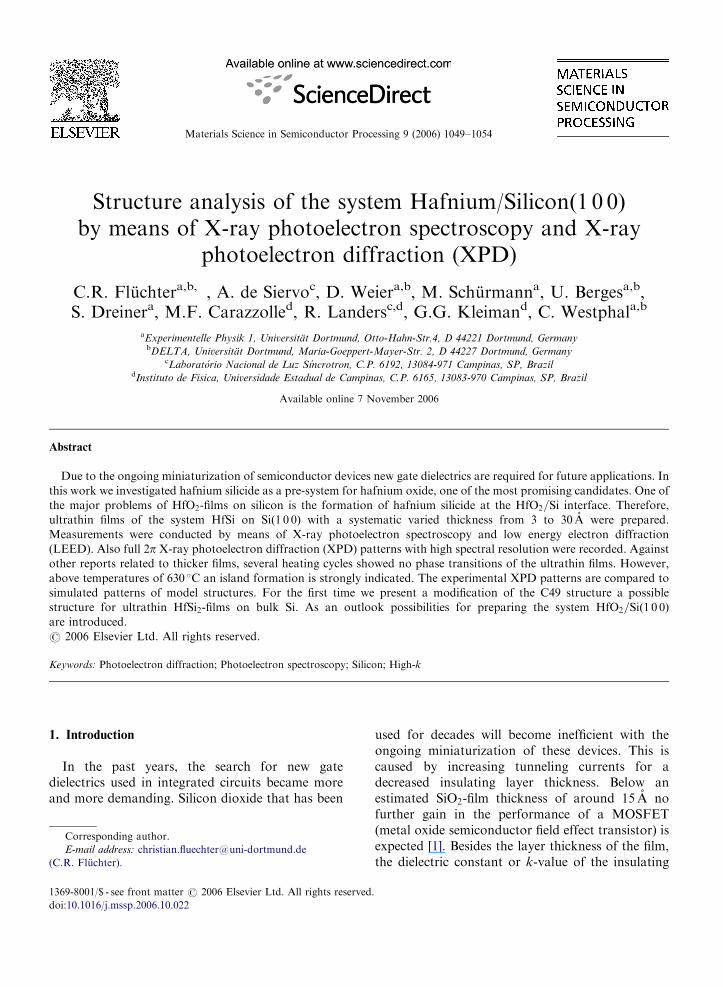
Fig. 1 shows the photoemission lines and normal-ized signal intensities of the Hf 4f and Si 2p signal asa function of the temperature. The thickness of theevaporated hafnium film was �30 A. Peak intensi-ties of the hafnium and silicon signals as a functionof the kinetic energy are displayed after removingthe secondary electrons background. The firstannealing at a temperature of T ¼ 500 �C leads toa 0.4 eV shift in the Hf signal in Fig. 1(a) to higherbinding energies. This can be interpreted as theinitial formation of a hafnium silicide phase [9].During the subsequent nine annealing steps attemperatures up to 945 �C no further shifts in thesignals were observed within the spectral resolutionof 0.7 eV. Fig. 1(a) also displays the Hf 4f signalafter the annealing cycle at T ¼ 880 �C. Chemicalshifts of the signal indicate further phase transitionsof the Hf-film. Such transitions, in this case fromHfSi to HfSi2, have been reported for much thickerfilms [10–12]. The behavior of the silicon signalduring the annealing sequence is shown in Fig. 1(b).In contrast to the hafnium peak a continuous gainof signal can be observed with respect to theannealing temperature. Finally, Fig. 1(c) shows thepeak area of the Si 2p and Hf 4f signals after severalannealing procedures. The annealing time was set to
ARTICLE IN PRESS
6000
4000
2000
0
1234 1236 1238
4000
3000
2000
1000
0
1150 1151 1152 1153
1.0
0.8
0.6
0.4
0.2
500 600 700 800 900
Temperature [°C]Kinetic Energy [eV]Kinetic Energy [eV]
inte
nsity
[arb
. uni
ts]
RT
880°C500°C
RT
880°C500°C
Hf 4f Si 2p Mg Kα
Hafnium 4fSilicon 2pclean Silicon
Nor
mal
ized
pea
k ar
ea
(a) (b) (c)
Fig. 1. Hf 4f (a) and Si 2p (b) XPS signals after annealing cycles of 60min. Peak area of Si and Hf signals as function of temperature (c).
C.R. Fluchter et al. / Materials Science in Semiconductor Processing 9 (2006) 1049–1054 1051
one hour for each cycle. Above a temperature ofaround 600 �C a sudden decrease in the hafniumsignal, together with an increase of the siliconsignal, is observed. Above 800 �C the slope of Sicurve flattens while there is a continuous loss of Hfsignal. For the high temperatures, the LEED imagesshowed a ð2� 1Þ reconstructed surface (not shown)with spot positions identical to the reconstructedsurface of clean silicon. A possible explanation isthat the annealing at temperatures above �630 �Cleads to the formation of HfSi2 islands on the siliconsurface. Between those islands, areas of exposedclean Si surface may appear, which would lead tothe ð2� 1Þ diffraction spots in LEED. This issupported by AFM studies on this system [10]wherein rectangular shaped islands could be ob-served on an annealed HfSi2 sample.
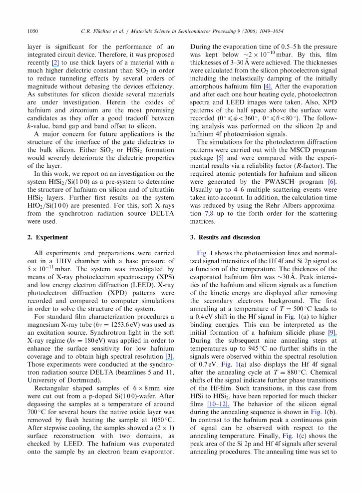
Photoelectron diffraction patterns were takenwith Mg Ka-radiation at different stages of theannealing sequence. Fig. 2(a) and (b) displaypatterns of the hafnium 4f peak after annealingcycles to 640 and 945 �C, respectively. Also, apattern with excitation of synchrotron radiation athn ¼ 180 eV is displayed for comparison (Fig. 2(c)).All three patterns represent the same structure. Thedifferent appearance of the patterns is a result of thedifferent electron wave-length and different surfacesensitivities. A more detailed analysis of photoelec-tron diffraction patterns recorded with synchrotronradiation is in preparation (see also [3]).
Another indication for the absence of a furthertransition within the ultrathin HfSi2 layers is
directly obtained by comparing the patterns ofFig. 2(a) and (b). Since the diffraction patternsoriginate directly from interference effects, they arevery sensitive to small structural changes in thesurface. As these two experimental patterns have anR-factor of R ¼ 0:05 with respect to each other, theycan be assumed as identical. The anisotropy thatmeasures the amplitude of the diffraction comparedto the overall signal also shows no significantdifference between the two patterns (13% in thesecond pattern compared to 16% in the first).
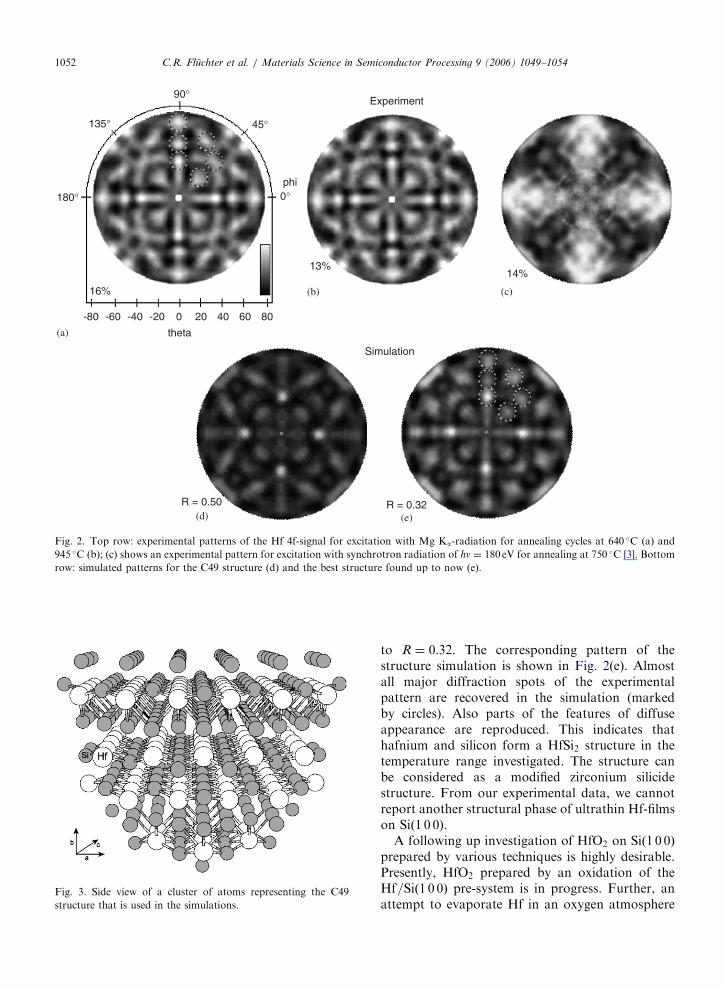
The C49 structure (also called zirconium silicidestructure) was chosen as a starting point for thecomputer simulations. This structure is displayed inFig. 3 and was found for bulk ZrSi2 and HfSi2. Thelattice parameters of a ¼ 3:677 A, b ¼ 14:550 A andc ¼ 3:649 A have been reported [13]. The first resultof the calculation conducted for the base structure isshown in Fig. 2(d), with an R-factor of R ¼ 0:5. Inthis first simulation no structure optimization wasapplied. Besides some similarities, many details aremissing in the intensity distribution compared to thepattern of Fig. 2(a).
In order to reduce the R-factor several parameterswere optimized. Generally, silicon terminated sur-faces showed a lower R-factor than Hf terminatedsurfaces. A relaxation of all lattice parameters led tono significant improvement in the R-factor, while asurface layer expansion of the lattice parameter b of10% reduced the R-factor significantly. Also,possible stacking faults 14 were included in thesimulations. As a result the R-factor was optimized
ARTICLE IN PRESS
180°
-80 -60 -40 -20 0 20 40 60 80
theta
16%
135°
90°
45°
0°
13%
phi
Experiment
14%
R = 0.50 R = 0.32
Simulation
(a)
(b) (c)
(d) (e)
Fig. 2. Top row: experimental patterns of the Hf 4f-signal for excitation with Mg Ka-radiation for annealing cycles at 640 �C (a) and
945 �C (b); (c) shows an experimental pattern for excitation with synchrotron radiation of hn ¼ 180 eV for annealing at 750 �C [3]. Bottom
row: simulated patterns for the C49 structure (d) and the best structure found up to now (e).
Fig. 3. Side view of a cluster of atoms representing the C49
structure that is used in the simulations.
C.R. Fluchter et al. / Materials Science in Semiconductor Processing 9 (2006) 1049–10541052
to R ¼ 0:32. The corresponding pattern of thestructure simulation is shown in Fig. 2(e). Almostall major diffraction spots of the experimentalpattern are recovered in the simulation (markedby circles). Also parts of the features of diffuseappearance are reproduced. This indicates thathafnium and silicon form a HfSi2 structure in thetemperature range investigated. The structure canbe considered as a modified zirconium silicidestructure. From our experimental data, we cannotreport another structural phase of ultrathin Hf-filmson Sið1 0 0Þ.
A following up investigation of HfO2 on Sið1 0 0Þprepared by various techniques is highly desirable.Presently, HfO2 prepared by an oxidation of theHf=Sið1 0 0Þ pre-system is in progress. Further, anattempt to evaporate Hf in an oxygen atmosphere

ARTICLE IN PRESS
Inte
nsity
[arb
. uni
ts]
90 92 94
Kinetic Energy [eV]
172 174 176 178 180 182Kinetic Energy [eV]
Si 2p
Si4+
hν = 200 eV
hν = 200 eVHf 4f
HfSi2
(a) (b)
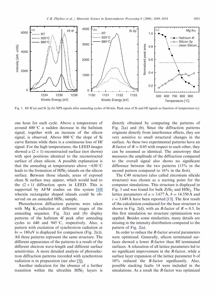
Fig. 4. Photoelectron spectra of the silicon 2p signal (a) and the hafnium 4f signal (b) after the direct evaporation of HfO2. No
contribution of SiO2 or HfSi2 is displayed.
C.R. Fluchter et al. / Materials Science in Semiconductor Processing 9 (2006) 1049–1054 1053
ðpox ¼ 1� 10�6 mbarÞ onto Sið1 0 0Þ was made, anda direct evaporation of HfO2 from an electronevaporator was checked, too. The sample wasalways kept at room temperature during thepreparations. The last method led to spectra withoutany Si4þ (i.e. silicon oxide) and without any hafniumsilicide component in the photoelectron spectra.Fig. 4 shows the spectra taken from this system withsynchrotron radiation and an excitation energy ofhn ¼ 200 eV. The sub-oxides of silicon in Fig. 4(a)originate probably from the HfO2=Si interface. Theabsence of hafnium silicate components in thehafnium spectrum may indicate that the HfO2 isbond to the substrate not via Si–Hf but Si–Obridges. The exact determination of the interface isthe goal of XPD simulations on this system. Thesystematic annealing of the system HfO2=Sið1 0 0Þand recording of the corresponding XPD patternswill be the next step in this investigation.
4. Conclusion
We investigated the system Hf=Sið1 0 0Þ withangle-scanned photoelectron diffraction and photo-electron spectroscopy with excitation energies ofhn ¼ 180 and 1253.6 eV. Subsequent annealingsequences showed no phase transitions of ultrathinHfSi2-films in the investigated temperature regimeof 600–945 �C. Computer simulations of the systemindicate the formation of a zirconium silicidestructure for all investigated films. A preparationtechnique avoiding silicon dioxide or hafnium
silicide formation was found by direct evaporationof HfO2 onto Sið1 0 0Þ.
Acknowledgments
This work is financially supported by the DAAD(No. 415-BR-PROBRAL-D-03-23553, Germany)and CAPES (Project PROBRAL 170/04, Brazil).Thanks goes to the staff of DELTA for continuessupport during the beametimes.
References
[1] Wilk G, Wallace R, Anthony J. High-k gate dielectrics:
current status and materials properties considerations.
J Appl Phys 2001;89(10):5243.
[2] Forst CJ, Ashman C, Schwarz K, Blochl P. The interface
between silicon and a high-k oxide. Nature 2004;427:53.
[3] Weier D, Fluchter CR, de Siervo A, Schurmann M, Dreiner
S, Berges U et al. Photoelectron spectroscopy (XPS) and
photoelectron diffraction (XPD) studies on the system
hafnium silicide and hafnium oxide on Sið1 0 0Þ. Phys Rev
B 2006;74:075319.
[4] Jablonski A, Powell C. Electron effective attenuation length
for applications in Auger electron spectroscopy and X-ray
photoelectron spectroscopy. Surf Sci Rep 2002;47:33.
[5] Chen Y, Hove MAV. MSCD package, Lawrence Berkeley
National Laboratory.
[6] Salvat F, Mayol R. Elastic scattering of electrons and
positrons by atoms. Schrodinger and dirac partial wave
analysis. Comput Phys Comm 1993;74:358–74.
[7] Rehr J, Albers R. Phys Rev B 1990;41:8139.
[8] Chen Y, de Abajo FJG, Chasse A, Ynzunza RX, Kaduwela
AP, Hove MAV, et al. Phys Rev B 1998;58(19):13121.

ARTICLE IN PRESSC.R. Fluchter et al. / Materials Science in Semiconductor Processing 9 (2006) 1049–10541054
[9] de Siervo A, Fluchter C, Weier D, Schurmann M, Dreiner S,
Carazzolle M, et al. The hafnium silicide formation on
Sið1 0 0Þ upon annealing. Phys Rev B 2006;74:1.
[10] Johnson-Steigelman HT, Brinck AV, Parihar SS, Lyman PF.
Hafnium silicide formation on Sið0 0 1Þ. Phys Rev B 2004;69:
235322.
[11] Lee J-H, Ichikawa M. Multiple phase structures of Hf
silicide precipitated from Hf silicate: an atomic view. J Vac
Sci Technol A 2002;20:1824.
[12] Ziegler JF, Mayer JW, Kircher CJ, Tu KN. Kinetics of the
formation of hafnium silicides on silicon. J Appl Phys 1973;
44(9):3851–7.
[13] Smith JF, Bailey DM. The structures of ZrGe2, HfSi2 and
HfGe2. Acta Cryst 1957;10:341.
[14] Bourett A, d’Heurie F, Goues FL, Charai A. Polytype
formation in zirconium–silicon thin films. J Appl Phys 1990;
67:1.
Related Documents


