Spartan-3 FPGA HDL Coding Techniques Part 1

Spartan-3 FPGA HDL Coding Techniques Part 1. Fundamentals of FPGA Design 1 day Designing for Performance 2 days Advanced FPGA Implementation 2 days Intro.
Dec 14, 2015
Welcome message from author
This document is posted to help you gain knowledge. Please leave a comment to let me know what you think about it! Share it to your friends and learn new things together.
Transcript

Spartan-3 FPGA HDL Coding Techniques
Part 1

Fundamentals of FPGA Design
1day
Designing forPerformance
2day
s
Advanced FPGAImplementation
2days
Intro to VHDL or Intro to Verilog
3days
FPGA and ASIC Technology Comparison
FPGA vs. ASIC Design Flow
ASIC to FPGACoding Conversion
Virtex-5 FPGA Coding Techniques Spartan-3 FPGA Coding Techniques
Curriculum Path
forASIC Design
FPGA and ASIC Technology Comparison
Welcome
This training will help you build efficient Spartan®-3 FPGA designs that have an efficient size and run at high speed
We will show you how to avoid some of the most common design mistakes
This content is essential if you have never coded a design for any 4-input LUT architecture or are converting an ASIC design
Objectives
After completing this module, you will be able to:
Optimize ASIC code for implementation in a Spartan-3 FPGA
Build a checklist of tips for optimizing your code for the Spartan-3 FPGA
Introduction
The design practices described in this module will make your design use fewer resources, run faster, and save you money– Can easily reduce the size of your design by 20% or MORE– A 20% reduction in size means that your design can fit into a
smaller device and have a faster implementation time– With the reduction in size it is likely that your design will run at
a higher system frequency and potentially save you from purchasing a faster speed grade device• Yes! You are free to run small, fast and at low cost!
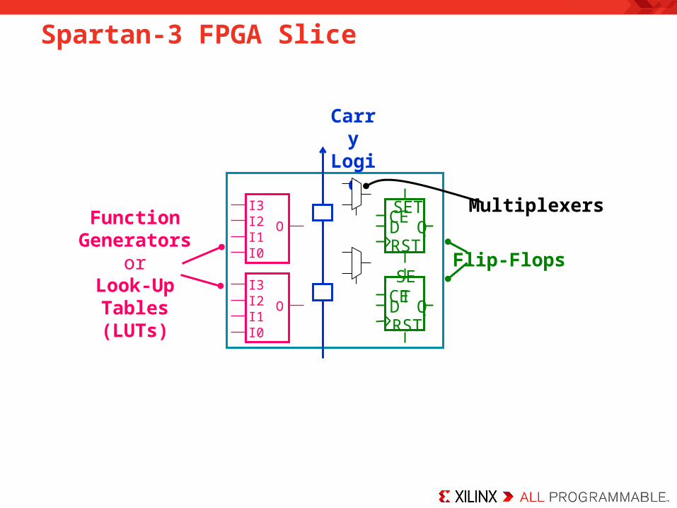
Spartan-3 FPGA Slice
Carry Logic
I3
I1I2
I0
O
I3
I1I2
I0
O D QSET
RST
CE
D QSET
RST
CE
Flip-Flops
Function Generators
orLook-Up Tables
(LUTs)
Multiplexers
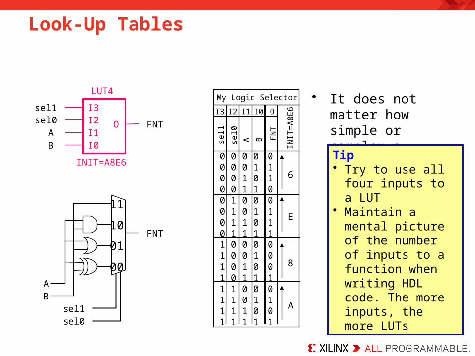
Look-Up Tables
0 0 0 00 0 0 10 0 1 00 0 1 10 1 0 00 1 0 10 1 1 00 1 1 11 0 0 01 0 0 11 0 1 01 0 1 11 1 0 01 1 0 11 1 1 01 1 1 1
INIT
=A8E
6I0I2 I1I3 O
A Bsel1
sel0
FNT
0110011100010101
A
8
E
6
My Logic SelectorI3
I1I2
I0
O
INIT=A8E6
AB
sel1sel0 FNT
00
11
10
01
AB
sel1sel0
FNT
LUT4 • It does not matter how simple or complex a function is, it is only limited by the inputs
Tip• Try to use all four inputs
to a LUT• Maintain a mental picture
of the number of inputs to a function when writing HDL code. The more inputs, the more LUTs
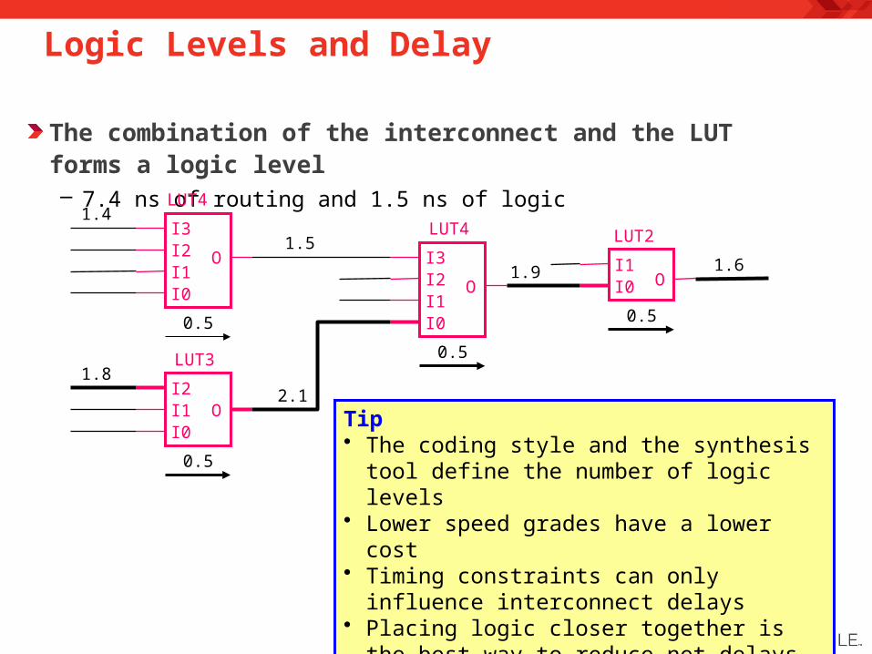
Logic Levels and Delay
The combination of the interconnect and the LUT forms a logic level– 7.4 ns of routing and 1.5 ns of logic
I3
I1I2
I0
O
LUT4
0.5
I1I2
I0O
LUT3
0.5
I3
I1I2
I0
O
LUT4
0.5
I1I0 O
LUT2
0.5
1.4
1.5
2.1
1.6
1.8
1.9
Tip • The coding style and the synthesis tool define the number
of logic levels• Lower speed grades have a lower cost• Timing constraints can only influence interconnect delays• Placing logic closer together is the best way to reduce net
delays
Tips
Try to maximize the number of inputs to each LUT so that you can obtain the most logic out of the FPGA
Instantiate the appropriate LUT primitive, if necessary– Refer to the Xilinx Unified Libraries Guide for primitive details
A logic level is one LUT plus one net delay
Synthesis tools and your coding style will determine how many logic levels there are in every path of your design
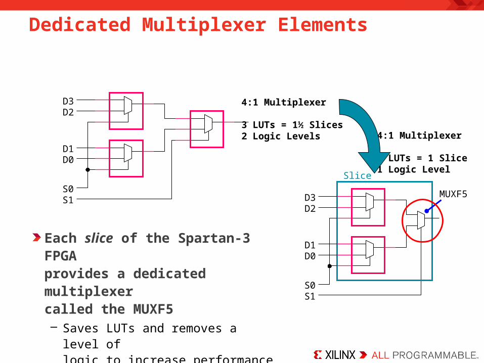
Dedicated Multiplexer Elements
Each slice of the Spartan-3 FPGA provides a dedicated multiplexer called the MUXF5– Saves LUTs and removes a level of
logic to increase performance
D3D2
D1D0
S0S1
4:1 Multiplexer
3 LUTs = 1½ Slices2 Logic Levels
D3D2
D1D0
S0S1
Slice
4:1 Multiplexer
2 LUTs = 1 Slice1 Logic Level
MUXF5
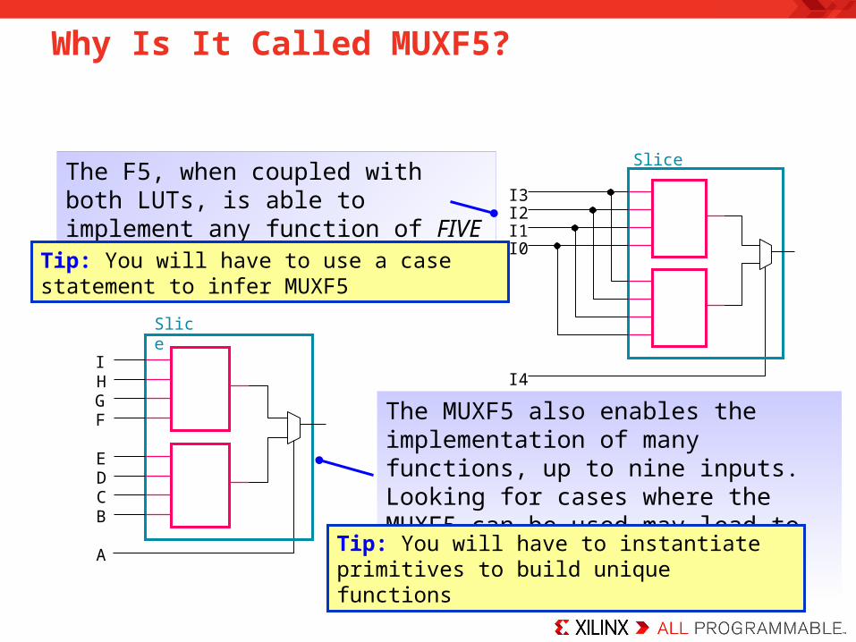
Why Is It Called MUXF5?
ED
A
Slice
The MUXF5 also enables the implementation of many functions, up to nine inputs. Looking for cases where the MUXF5 can be used may lead to lower cost and higher performanceC
B
IHGF
Slice
I3
I1I2
I0
I4
The F5, when coupled with both LUTs, is able to implement any function of FIVE inputs
Tip: You will have to instantiate primitives to build unique functions
Tip: You will have to use a case statement to infer MUXF5
Building Larger Multiplexers
S2S1S0
F5
D0D1
D2D3
F5
D4D5
D6D7
Fx F6
F5
D8D9
D10D11
F5
D12D13
D14D15
F7 F6
S3
S4
F5
D16D17
D18D19
F5
D20D21
D22D23
F8 F6
F5
D24D25
D26D27
F5
D28D29
D30D31
F7 F6
4:1 Multiplexer 1 Slice (MUXF5)
8:1 Multiplexer 2 Slices (MUXF6)
16:1 Multiplexer 4 Slices (MUXF7)
32:1 Multiplexer 8 Slices (MUXF8)
Using the F6, F7, and F8Will need a case statement
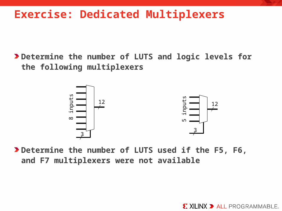
Exercise: Dedicated Multiplexers
Determine the number of LUTS and logic levels for the following multiplexers
Determine the number of LUTS used if the F5, F6, and F7 multiplexers were not available
12
3
12
3
8 in
puts
5 in
puts
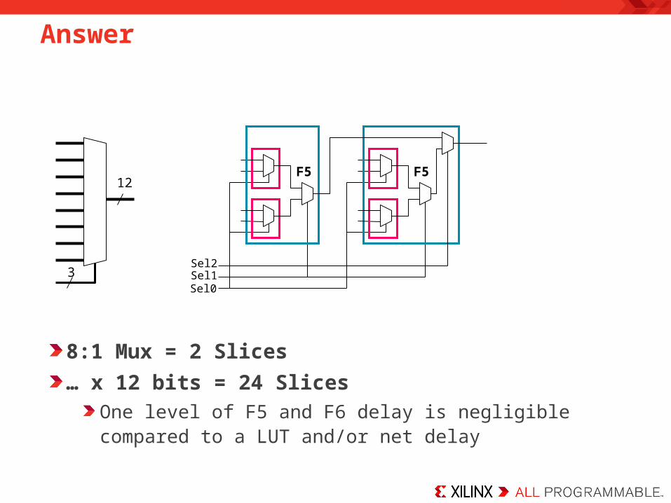
Answer
12
3Sel2Sel1Sel0
F5 F5
8:1 Mux = 2 Slices
… x 12 bits = 24 Slices
One level of F5 and F6 delay is negligible compared to a LUT and/or net delay
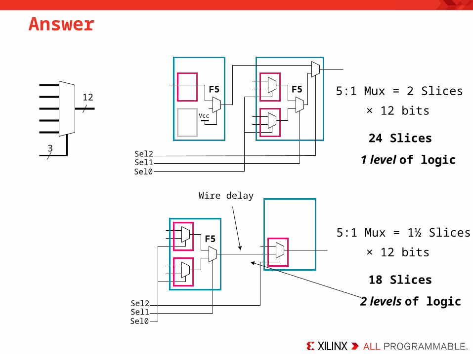
Answer
5:1 Mux = 2 Slices
24 Slices
× 12 bits
1 level of logic
Sel2Sel1Sel0
F5
Wire delay
12
3Sel2Sel1Sel0
F5 F5
Vcc
5:1 Mux = 1½ Slices
18 Slices
× 12 bits
2 levels of logic
Tips
The F5, F6, F7, and F8 multiplexers build large, fast multiplexers– These resources are fast in logic and routing
To infer these resources, you will need to use a case statement in your HDL code– Verify with your schematic viewer whether they were inferred correctly
Inference of unique functions will probably require instantiating the appropriate multiplexer primitives– Refer to the Xilinx Unified Libraries Guide for primitive details
To break a large multiplexer down into smaller sections for pipelining, be sure to break into 4:1 and 8:1 multiplexers
Enhanced Register
Virtex® FPGA-based registers provide clock enables, set, and resets ports directly on the register– Sets and resets can be programmed as synchronous or asynchronous and
must match
All three can be used on any register– To directly use the pins on the register, the priority must be: Reset, Set, CE
By having these pins directly on the register, the fan-in to the LUT is reduced– Without a direct pin on the register, these functions would be implemented
through the LUT before the register (that is, you would lose one LUT input)
Enhanced Register Example
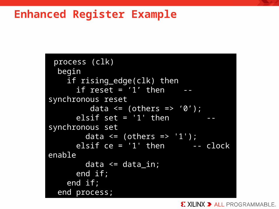
process (clk) begin if rising_edge(clk) then if reset = ‘1’ then -- synchronous reset data <= (others => ‘0’); elsif set = '1' then -- synchronous set data <= (others => '1'); elsif ce = '1' then -- clock enable data <= data_in; end if; end if; end process;
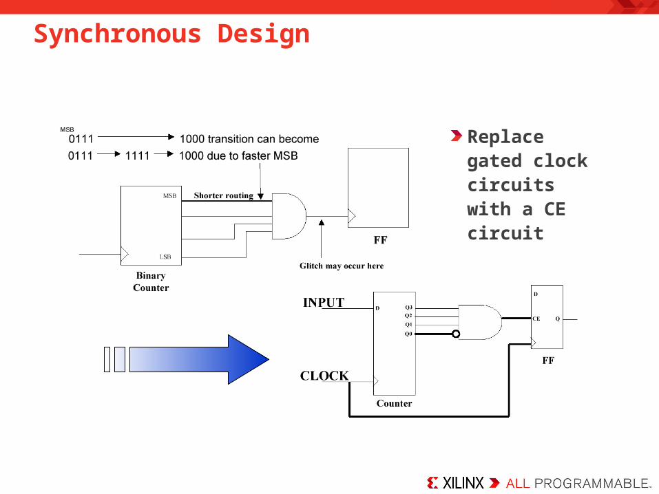
Synchronous Design
Replace gated clock circuits with a CE circuit
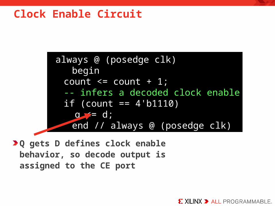
Clock Enable Circuit
always @ (posedge clk) begin
count <= count + 1;-- infers a decoded clock enableif (count == 4'b1110) q <= d;
end // always @ (posedge clk)
Q gets D defines clock enable behavior, so decode output is assigned to the CE port
Synchronous Reset
Synchronous Set and Reset
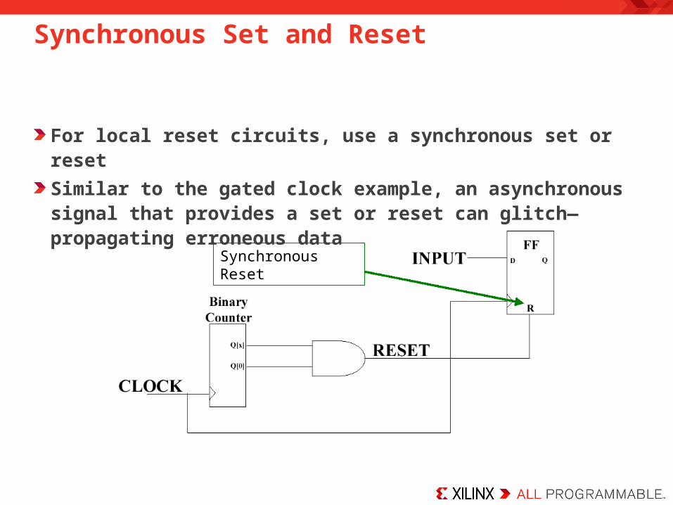
For local reset circuits, use a synchronous set or reset
Similar to the gated clock example, an asynchronous signal that provides a set or reset can glitch—propagating erroneous data
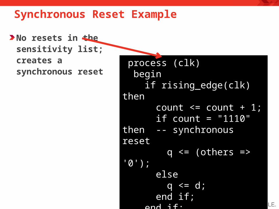
Synchronous Reset Example
process (clk) begin if rising_edge(clk) then count <= count + 1; if count = "1110" then -- synchronous reset q <= (others => '0'); else q <= d; end if; end if; end process;
No resets in the sensitivity list; creates a synchronous reset
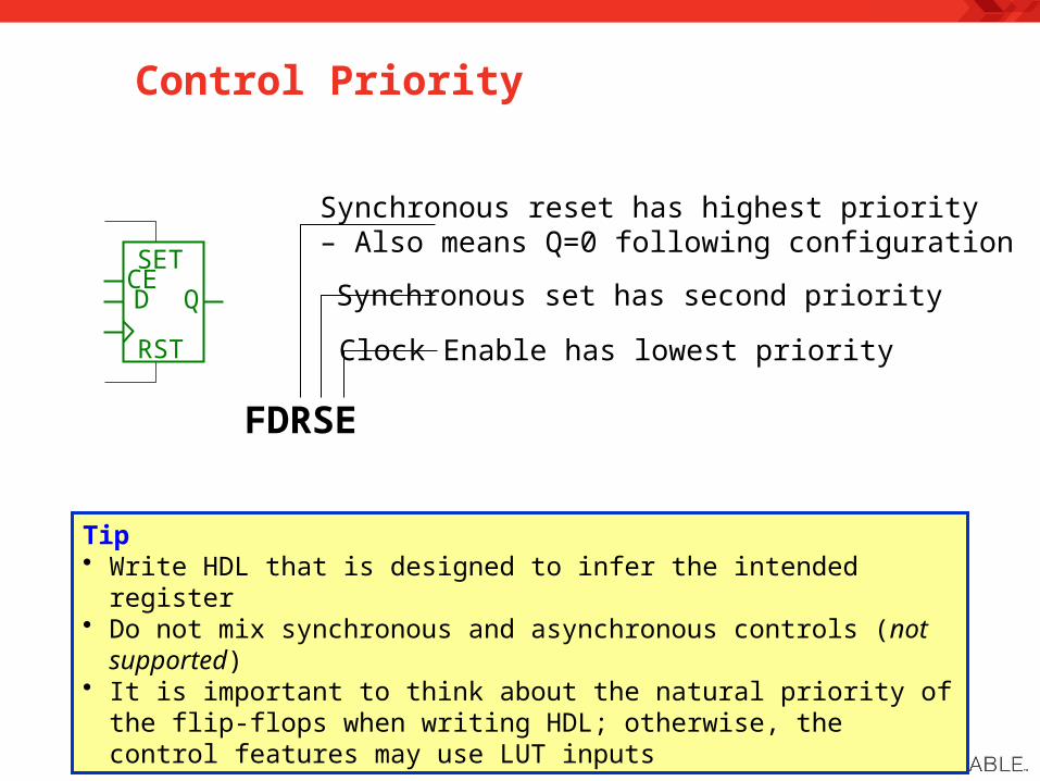
Control Priority
D Q
SET
RST
CE
FDRSE
Synchronous set has second priority
Clock Enable has lowest priority
Synchronous reset has highest priority– Also means Q=0 following configuration
Tip• Write HDL that is designed to infer the intended register• Do not mix synchronous and asynchronous controls (not supported)• It is important to think about the natural priority of the flip-flops when writing HDL;
otherwise, the control features may use LUT inputs
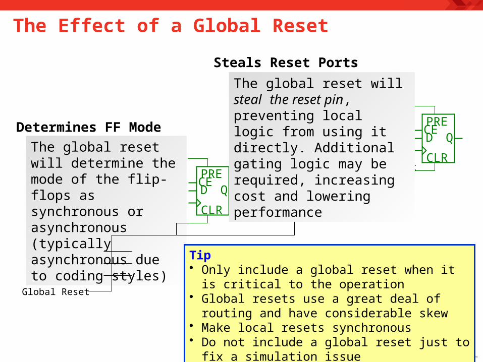
The Effect of a Global Reset
D QPRE
CLR
CE
Global Reset
D QPRE
CLR
CE
Local Reset net
Determines FF Mode
The global reset will determine the mode of the flip-flops as synchronous or asynchronous (typically asynchronous due to coding styles)
Tip• Only include a global reset when it is critical to the operation• Global resets use a great deal of routing and have
considerable skew• Make local resets synchronous• Do not include a global reset just to fix a simulation issue
The global reset will steal the reset pin, preventing local logic from using it directly. Additional gating logic may be required, increasing cost and lowering performance
Steals Reset Ports
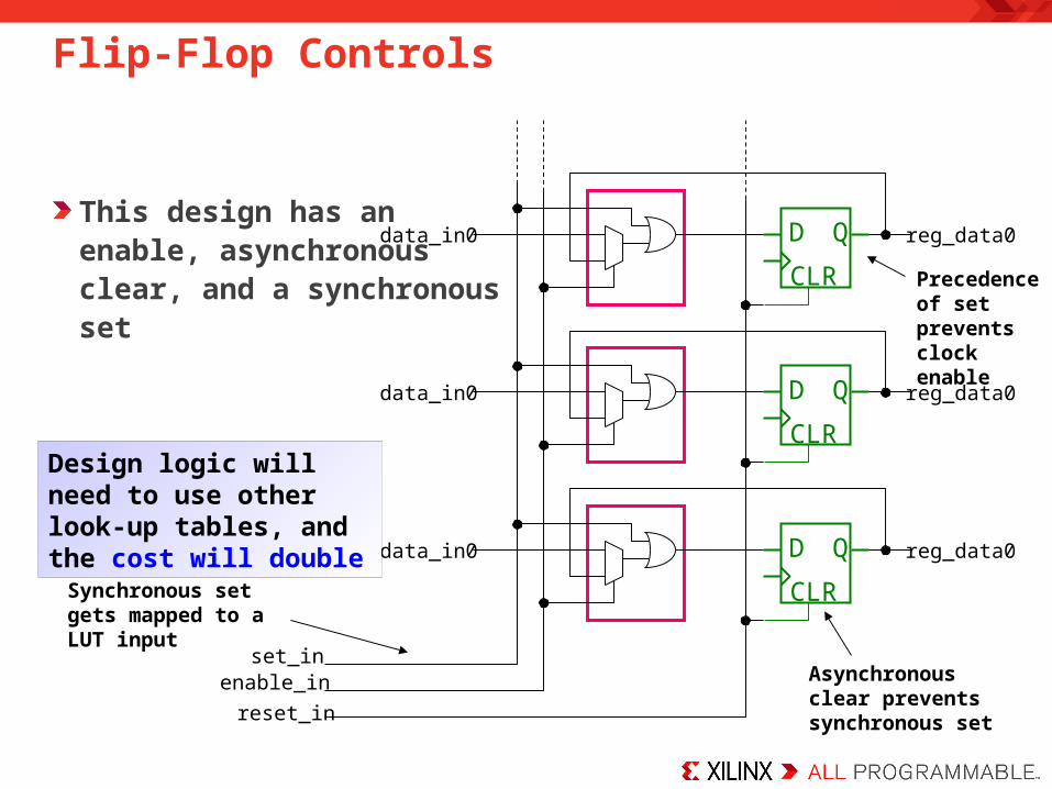
Flip-Flop Controls
This design has an enable, asynchronous clear, and a synchronous set
D Q
CLR
reset_in
reg_data0
set_in
data_in0
Asynchronous clear prevents synchronous set
enable_in
Precedence of set prevents clock enable
D Q
CLR
reg_data0data_in0
D Q
CLR
reg_data0data_in0
Design logic will need to use other look-up tables, and the cost will double
Synchronous set gets mapped to a LUT input
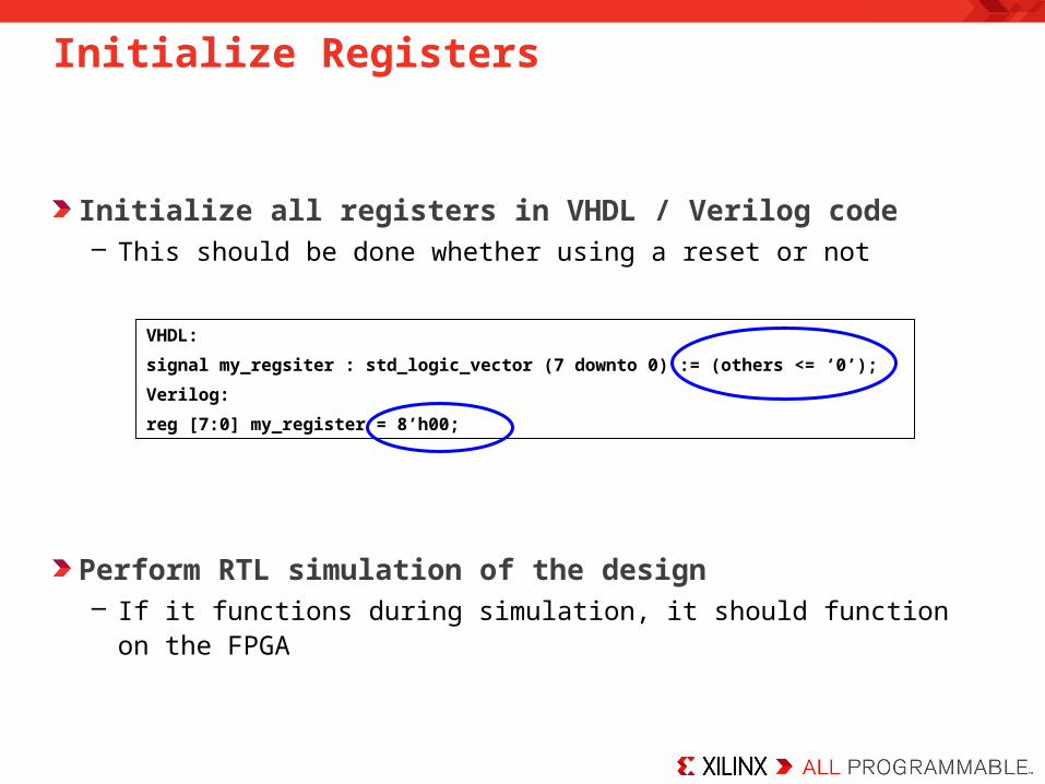
Initialize Registers
Initialize all registers in VHDL / Verilog code– This should be done whether using a reset or not
Perform RTL simulation of the design– If it functions during simulation, it should function on the FPGA
VHDL:
signal my_regsiter : std_logic_vector (7 downto 0) := (others <= ‘0’);
Verilog:
reg [7:0] my_register = 8’h00;
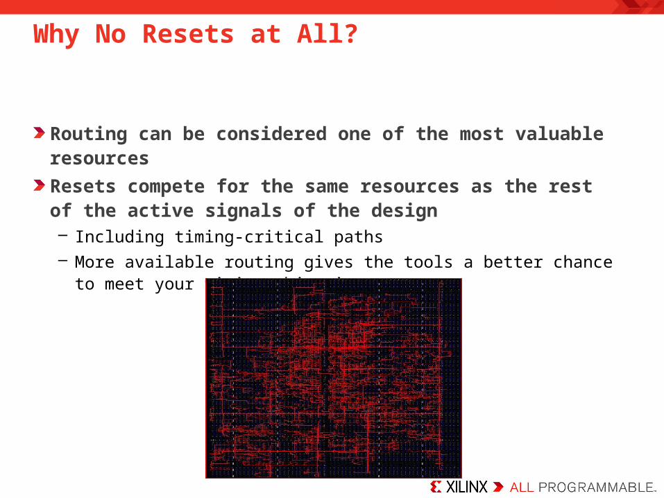
Why No Resets at All?
Routing can be considered one of the most valuable resources
Resets compete for the same resources as the rest of the active signals of the design – Including timing-critical paths– More available routing gives the tools a better chance to meet your timing
objectives
Why No Resets at All?
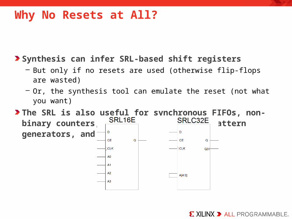
Synthesis can infer SRL-based shift registers– But only if no resets are used (otherwise flip-flops are wasted)– Or, the synthesis tool can emulate the reset (not what you want)
The SRL is also useful for synchronous FIFOs, non-binary counters, terminal count logic, pattern generators, and reconfigurable LUTs
Why No Resets at All?
Designs without resets have fewer timing paths– By an average of 18 percent fewer timing paths– This is important when you consider that synchronous reset paths are
automatically timed (this is not a bad thing)• Asynchronous reset paths are NOT timed
Results in less run time
Improved performance
Less memory necessary during PAR
Tips
Try to manage the number of control signals in your designAll three control ports can be used on any register– To directly use the pins on the register, the priority must be: Reset, Set,
CE
Do not gate your clock– It will not operate reliably– Map this functionality to the CE port
Do not build with an asynchronous reset– It will not operate reliably if it is local– Global asynchronous reset might work, but it might waste LUTs and
create a long net delay
Do not mix asynchronous and synchronous control signals on the same registerDo not use a global reset to make simulation easier– Initialize your registers in HDL
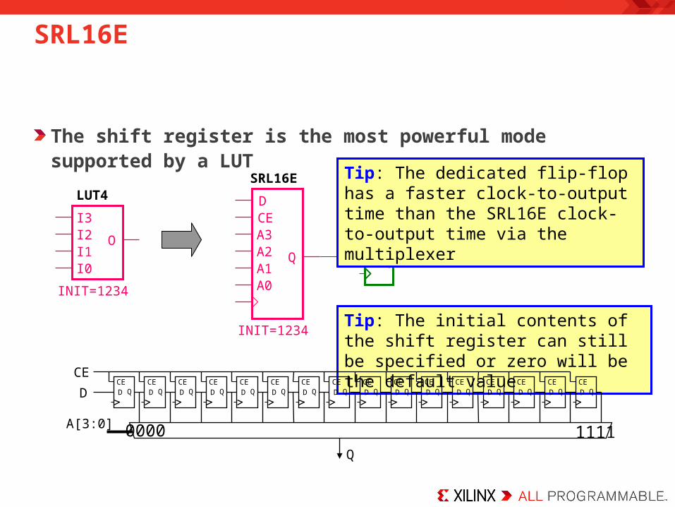
SRL16E
The shift register is the most powerful mode supported by a LUT
I3
I1I2
I0
O
INIT=1234
LUT4
Tip: The initial contents of the shift register can still be specified or zero will be the default value
D QA3
A1A2
A0
Q
CE
INIT=1234
SRL16E
D
Tip: The dedicated flip-flop has a faster clock-to-output time than the SRL16E clock-to-output time via the multiplexer
D
CECE
QDCE
QDCE
QDCE
QDCE
QDCE
QDCE
QDCE
QDCE
QDCE
QDCE
QDCE
QDCE
QDCE
QDCE
QDCE
QD
A[3:0] 0000 1111Q
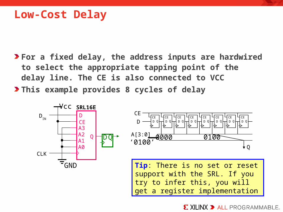
For a fixed delay, the address inputs are hardwired to select the appropriate tapping point of the delay line. The CE is also connected to VCC
This example provides 8 cycles of delay
Low-Cost Delay
D
CECE
QDCE
QDCE
QDCE
QDCE
QDCE
QDCE
QDCE
QD
A[3:0] 0000Q
‘0100’
A3
A1A2
A0
Q
CE
D Q
DDIN
CLK
SRL16EVcc
GND
0100
Tip: There is no set or reset support with the SRL. If you try to infer this, you will get a register implementation
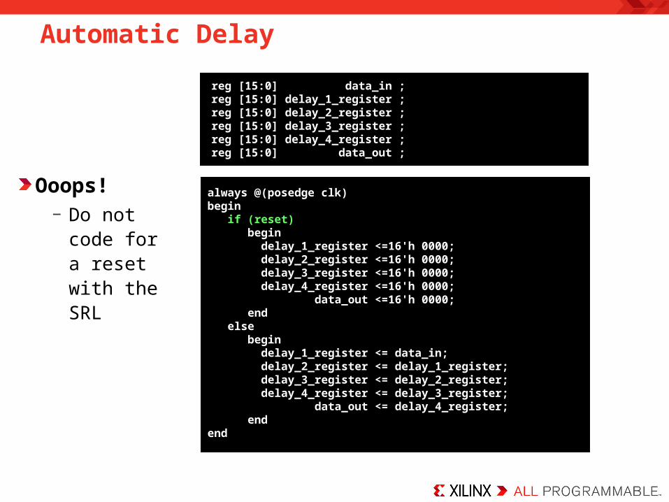
Automatic Delay
always @(posedge clk)begin if (reset) begin delay_1_register <=16'h 0000; delay_2_register <=16'h 0000; delay_3_register <=16'h 0000; delay_4_register <=16'h 0000; data_out <=16'h 0000; end else begin delay_1_register <= data_in; delay_2_register <= delay_1_register; delay_3_register <= delay_2_register; delay_4_register <= delay_3_register; data_out <= delay_4_register; end end
reg [15:0] data_in ; reg [15:0] delay_1_register ;reg [15:0] delay_2_register ;reg [15:0] delay_3_register ;reg [15:0] delay_4_register ;reg [15:0] data_out ;
Ooops!− Do not code
for a reset with the SRL
Automatic Delay
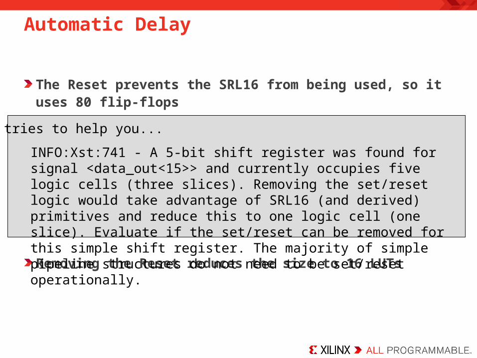
The Reset prevents the SRL16 from being used, so it uses 80 flip-flops
Removing the Reset reduces the size to 16 LUTs
INFO:Xst:741 - A 5-bit shift register was found for signal <data_out<15>> and currently occupies five logic cells (three slices). Removing the set/reset logic would take advantage of SRL16 (and derived) primitives and reduce this to one logic cell (one slice). Evaluate if the set/reset can be removed for this simple shift register. The majority of simple pipeline structures do not need to be set/reset operationally.
XST tries to help you...
Tips
The SRL is an effective means of delaying a datapath– 1 LUT = 16 flip-flops
The SRL supports CE and initialization of its contents
The SRL does NOT support set or reset functionality– If you code for set or reset, you will get a register implementation– This is a waste of registers
The SRL is serial in/serial out– If you code for a parallel read, you will get a register implementation
Experiment with your synthesis tool to determine if it will give you a similar warning to what XST gives you
Summary
To infer the dedicated multiplexer resources you will need to use a case statement in your HDL code– Verify with your schematic viewer whether they were inferred correctly
If you plan to break a large multiplexer down into smaller sections in order to pipeline, be sure to break into 4:1 and 8:1 multiplexers
All three control ports can be used on any register– To directly use the pins on the register, the priority must be: Reset, Set, CE
Do not mix asynchronous and synchronous control signals on the same register
Summary
The SRL does not support set or reset functionality– If you code for set or reset, you will get a register implementation– This is a waste of registers
The SRL is serial in/serial out– If you code for a parallel read, you will get a register implementation
Avoid global resets– If you cannot avoid global asynchronous resets, be aware that also using
local synchronous resets will end up using more LUTs– Local synchronous reset creates a high fanout net (that might create timing
problems) when there is also a global asynchronous reset

Where Can I Learn More?
Xilinx Online Documents – support.xilinx.com
• To search for an Application Note or White Paper, click the Documentation tab and enter the document number (WP231 or XAPP215) in the search window
• White papers for reference WP275 – Get your Priorities Right – Make your Design Up to 50%
Smaller WP272 – Get Smart About Reset: Think Local, Not Global
• Xilinx Unified Library Guide From the ISE® Design Suite, select Help Software Manuals
Additional Online Training– www.xilinx.com/training

Spartan-3 FPGA HDL Coding Techniques
Part 2

Fundamentals of FPGA Design
1day
Designing forPerformance
2day
s
Advanced FPGAImplementation
2days
Intro to VHDL or Intro to Verilog
3days
FPGA and ASIC Technology Comparison
FPGA vs. ASIC Design Flow
ASIC to FPGACoding Conversion
Virtex-5 FPGA Coding Techniques Spartan-3 FPGA Coding Techniques
Curriculum Path
forASIC Design
FPGA and ASIC Technology Comparison

Welcome
This training will help you build efficient Spartan®-3 FPGA designs that have an efficient size and run at high speed
We will show you how to avoid some of the most common design mistakes
This content is essential if you have never coded a design for any 4-input LUT architecture or are converting an ASIC design

Objectives
After completing this module, you will be able to:
Optimize ASIC code for implementation in a Spartan-3 FPGA
Build a checklist of tips for optimizing your code for the Spartan-3 FPGA
Inference of Arithmetic Logic
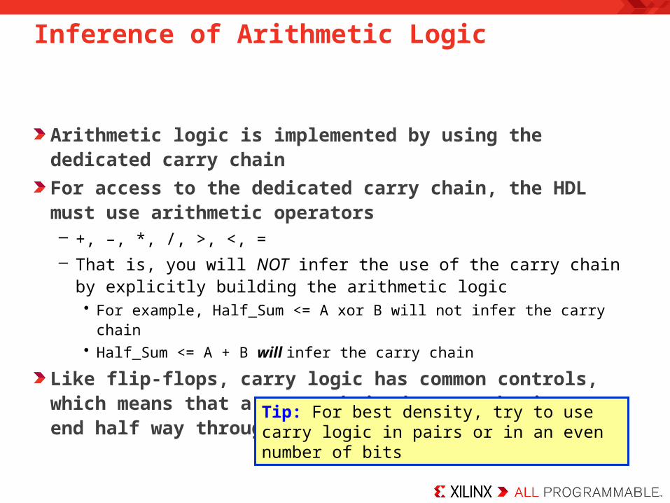
Arithmetic logic is implemented by using the dedicated carry chain
For access to the dedicated carry chain, the HDL must use arithmetic operators– +, –, *, /, >, <, =– That is, you will NOT infer the use of the carry chain by explicitly building
the arithmetic logic• For example, Half_Sum <= A xor B will not infer the carry chain• Half_Sum <= A + B will infer the carry chain
Like flip-flops, carry logic has common controls, which means that a carry chain does not begin or end half way through a slice
Tip: For best density, try to use carry logic in pairs or in an even number of bits
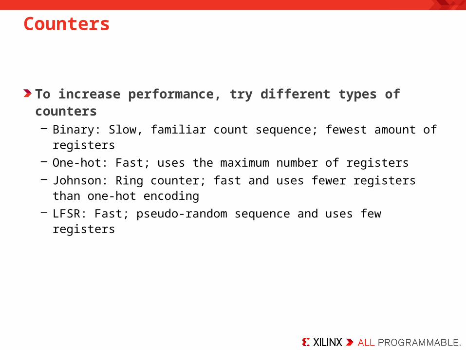
Counters
To increase performance, try different types of counters– Binary: Slow, familiar count sequence; fewest amount of registers– One-hot: Fast; uses the maximum number of registers– Johnson: Ring counter; fast and uses fewer registers than one-hot
encoding– LFSR: Fast; pseudo-random sequence and uses few registers
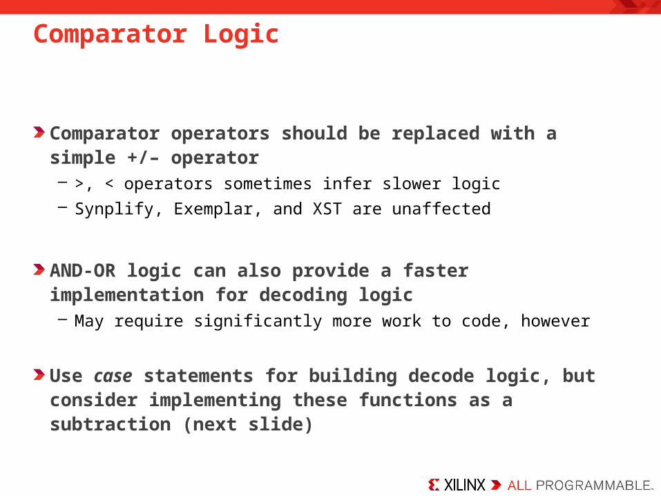
Comparator Logic
Comparator operators should be replaced with a simple +/– operator– >, < operators sometimes infer slower logic– Synplify, Exemplar, and XST are unaffected
AND-OR logic can also provide a faster implementation for decoding logic– May require significantly more work to code, however
Use case statements for building decode logic, but consider implementing these functions as a subtraction (next slide)
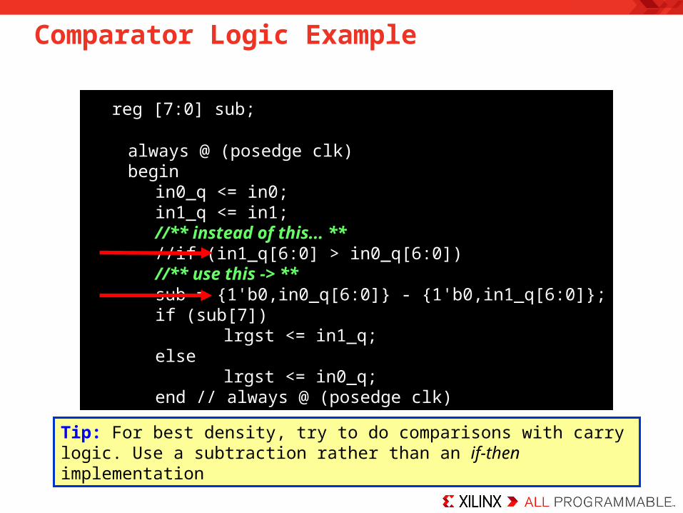
Comparator Logic Example
reg [7:0] sub; always @ (posedge clk) begin
in0_q <= in0;in1_q <= in1;//** instead of this... **//if (in1_q[6:0] > in0_q[6:0])//** use this -> **sub = {1'b0,in0_q[6:0]} - {1'b0,in1_q[6:0]};if (sub[7])
lrgst <= in1_q;else
lrgst <= in0_q; end // always @ (posedge clk)
Tip: For best density, try to do comparisons with carry logic. Use a subtraction rather than an if-then implementation
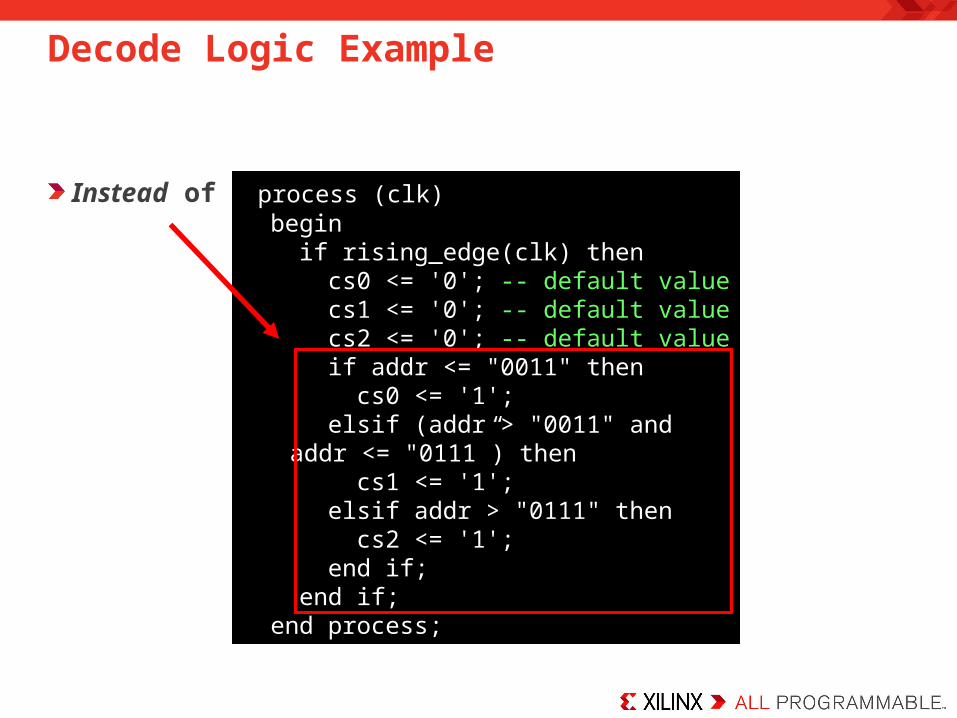
Decode Logic Example
Instead of this process (clk) begin if rising_edge(clk) then cs0 <= '0'; -- default value cs1 <= '0'; -- default value cs2 <= '0'; -- default value if addr <= "0011" then cs0 <= '1'; elsif (addr > "0011" and
addr <= "0111”) then cs1 <= '1'; elsif addr > "0111" then cs2 <= '1'; end if; end if; end process;
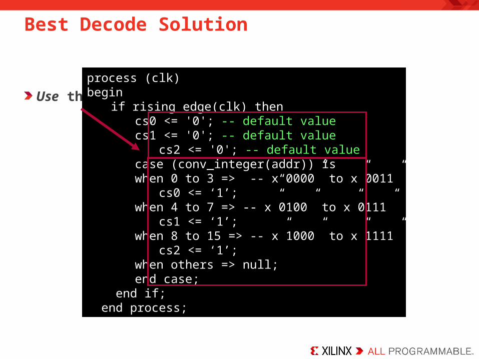
Best Decode Solution
Use this
process (clk)begin
if rising_edge(clk) thencs0 <= '0'; -- default value cs1 <= '0'; -- default value
cs2 <= '0'; -- default valuecase (conv_integer(addr)) iswhen 0 to 3 => -- x“0000” to x”0011”
cs0 <= ‘1’;when 4 to 7 => -- x”0100” to x”0111”
cs1 <= ‘1’;when 8 to 15 => -- x”1000” to x”1111”
cs2 <= ‘1’;when others => null;end case;
end if; end process;
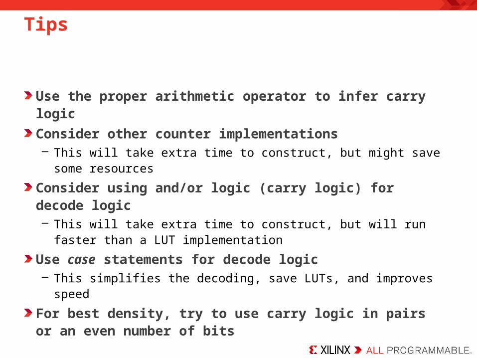
Tips
Use the proper arithmetic operator to infer carry logic
Consider other counter implementations– This will take extra time to construct, but might save some resources
Consider using and/or logic (carry logic) for decode logic– This will take extra time to construct, but will run faster than a LUT
implementation
Use case statements for decode logic– This simplifies the decoding, save LUTs, and improves speed
For best density, try to use carry logic in pairs or an even number of bits
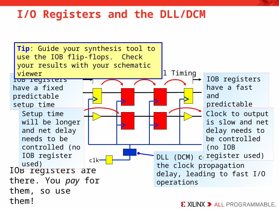
I/O Registers and the DLL/DCM
IOB registers are there. You pay for them, so use them!
DLL (DCM) compensates for the clock propagation delay, leading to fast I/O operations
clk
IOB registers have a fixed predictable setup time
Simple Internal TimingIOB registers have a fast and predictable clock-to-output time
Clock to output is slow and net delay needs to be controlled (no IOB register used)
Setup time will be longer and net delay needs to be controlled (no IOB register used)
Tip: Guide your synthesis tool to use the IOB flip-flops. Check your results with your schematic viewer
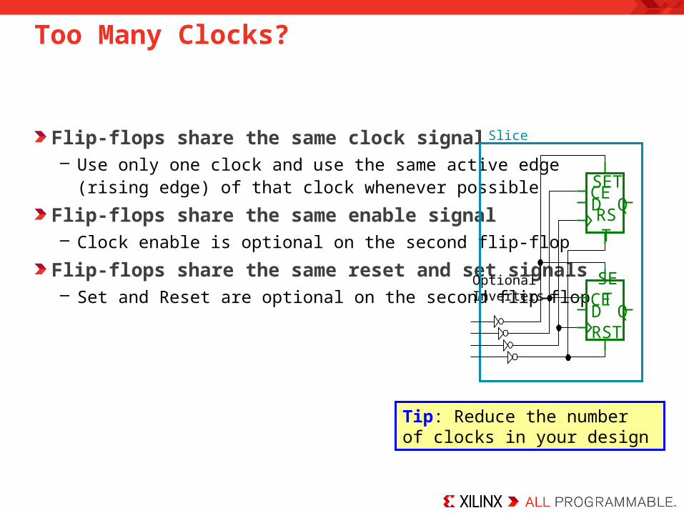
Too Many Clocks?
Flip-flops share the same clock signal– Use only one clock and use the same active edge
(rising edge) of that clock whenever possible
Flip-flops share the same enable signal– Clock enable is optional on the second flip-flop
Flip-flops share the same reset and set signals– Set and Reset are optional on the second flip-flop
D QSET
RST
CE
D QSET
RST
CE
Slice
OptionalInverters
Tip: Reduce the number of clocks in your design

Apply Your Knowledge
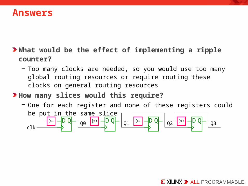
What would be the effect of implementing a ripple counter?
How many slices would this require?
D Q D Q D Q D Qclk
Q0 Q1 Q2 Q3
Answers
What would be the effect of implementing a ripple counter?– Too many clocks are needed, so you would use too many global routing
resources or require routing these clocks on general routing resources
How many slices would this require?– One for each register and none of these registers could be put in the same
slice
D Q D Q D Q D Qclk
Q0 Q1 Q2 Q3
Apply Your Knowledge
In this design you are using a simple synchronous reset with a counter
How will your counter implementationbe affected if the design also includes a global asynchronous reset signal?
0 1
D Q
0 1
D Q
Q0
Q1
0 1
D Q Q2
always @(posedge clk)begin if (reset_in)
q <= 8'h00; else
q <= q + 1'b1;end
reg [8:0] q;
0 1
D Q
0 1
D Q
Q0
Q1
0 1
D Q Q2
global_reset
FDC
FDC
FDC
sync_reset
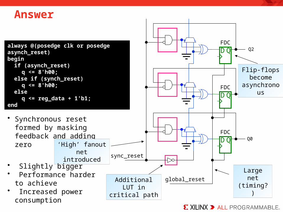
• Synchronous reset formed by masking feedback and adding zero
Additional LUT in critical path
‘High’ fanout net introduced
• Slightly bigger• Performance harder to achieve• Increased power consumption
Large net(timing?)
Flip-flops become
asynchronous
always @(posedge clk or posedge asynch_reset)begin if (asynch_reset)
q <= 8'h00; else if (synch_reset)
q <= 8'h00; else
q <= reg_data + 1'b1;end
Answer
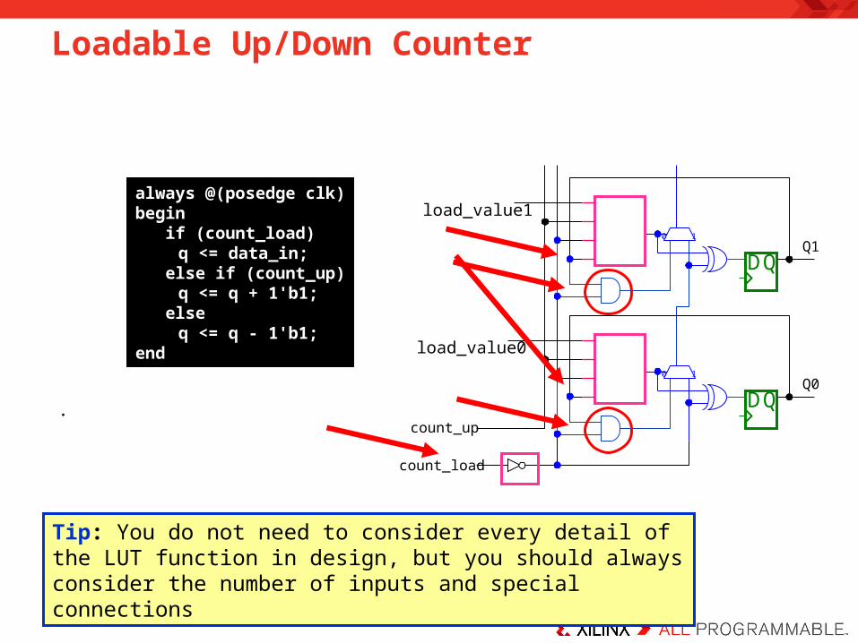
Loadable Up/Down Counter
Tip: You do not need to consider every detail of the LUT function in design, but you should always consider the number of inputs and special connections
. Q0
0 1
count_load
D Q
Q10 1
D Q
load_value0
load_value1
count_up
always @(posedge clk)begin if (count_load)
q <= data_in; else if (count_up)
q <= q + 1'b1; else
q <= q - 1'b1;end
Tips
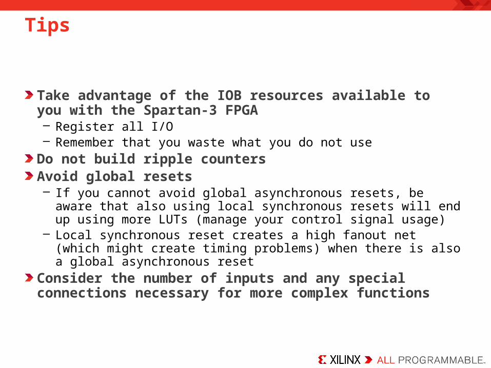
Take advantage of the IOB resources available to you with the Spartan-3 FPGA– Register all I/O– Remember that you waste what you do not use
Do not build ripple countersAvoid global resets– If you cannot avoid global asynchronous resets, be aware that also using
local synchronous resets will end up using more LUTs (manage your control signal usage)
– Local synchronous reset creates a high fanout net (which might create timing problems) when there is also a global asynchronous reset
Consider the number of inputs and any special connections necessary for more complex functions
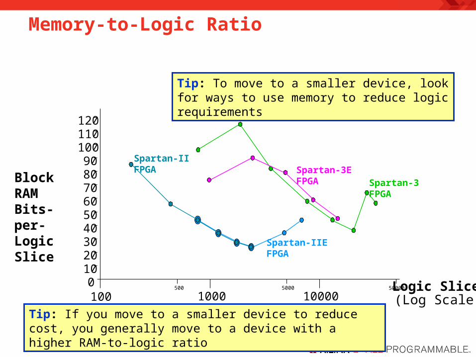
Memory-to-Logic Ratio
Logic Slices
Block RAM Bits-per-Logic Slice
010
120
100 1000500
100005000 50000
2030405060708090
100110
Spartan-IIEFPGA
Spartan-IIFPGA
Spartan-3FPGA
(Log Scale)
Spartan-3EFPGA
Tip: If you move to a smaller device to reduce cost, you generally move to a device with a higher RAM-to-logic ratio
Tip: To move to a smaller device, look for ways to use memory to reduce logic requirements
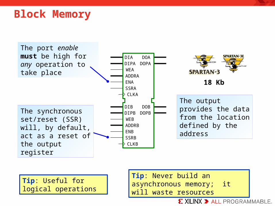
18 Kb
The port enable must be high for any operation to take place
CLKA
DIPA
ADDRA
DOPAWEA
CLKB
ADDRBWEB
ENASSRA
ENBSSRB
DIA DOA
DIPB DOPBDIB DOB
The synchronous set/reset (SSR) will, by default, act as a reset of the output register
Tip: Useful for logical operationsTip: Never build an asynchronous memory; it will waste resources
The output provides the data from the location defined by the address
Block Memory
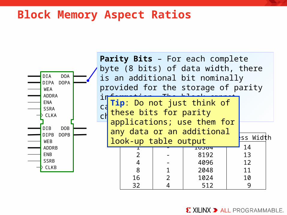
Block Memory Aspect Ratios
CLKA
DIPA
ADDRA
DOPAWEA
CLKB
ADDRBWEB
ENASSRA
ENBSSRB
163848192409620481024 512
Data Width Memory Locations Address Width1248
1632
1413121110 9
Parity Bits---124
DIA DOA
DIPB DOPBDIB DOB
Parity Bits – For each complete byte (8 bits) of data width, there is an additional bit nominally provided for the storage of parity information. The block cannot calculate or perform parity checking
Tip: Do not just think of these bits for parity applications; use them for any data or an additional look-up table output
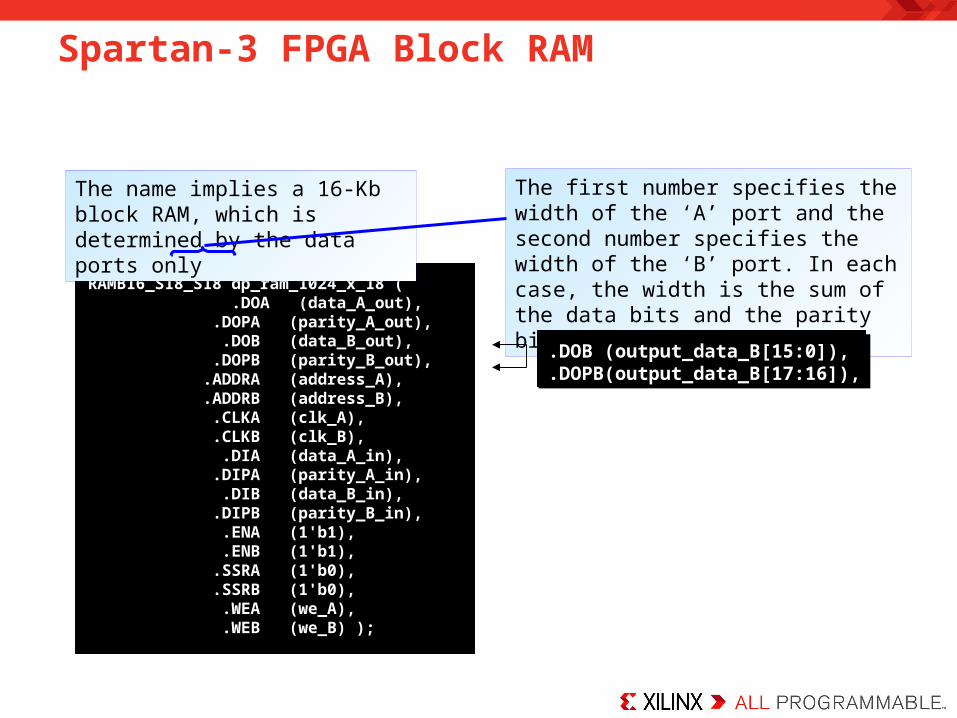
Spartan-3 FPGA Block RAM
RAMB16_S18_S18 dp_ram_1024_x_18 ( .DOA (data_A_out), .DOPA (parity_A_out), .DOB (data_B_out), .DOPB (parity_B_out), .ADDRA (address_A), .ADDRB (address_B), .CLKA (clk_A), .CLKB (clk_B), .DIA (data_A_in), .DIPA (parity_A_in), .DIB (data_B_in), .DIPB (parity_B_in), .ENA (1'b1), .ENB (1'b1), .SSRA (1'b0), .SSRB (1'b0), .WEA (we_A), .WEB (we_B) );
The name implies a 16-Kb block RAM, which is determined by the data ports only
The first number specifies the width of the ‘A’ port and the second number specifies the width of the ‘B’ port. In each case, the width is the sum of the data bits and the parity bits
.DOB (output_data_B[15:0]),
.DOPB(output_data_B[17:16]),
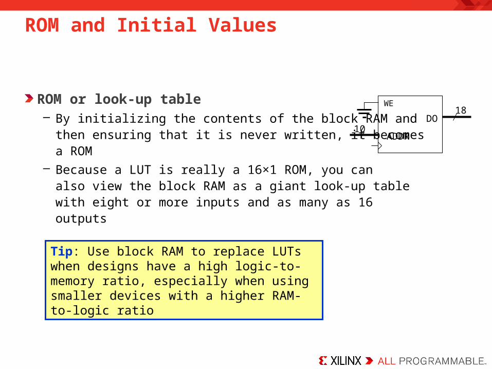
ROM and Initial Values
ROM or look-up table – By initializing the contents of the block RAM and
then ensuring that it is never written, it becomes a ROM
– Because a LUT is really a 16×1 ROM, you can also view the block RAM as a giant look-up table with eight or more inputs and as many as 16 outputs
Tip: Use block RAM to replace LUTs when designs have a high logic-to-memory ratio, especially when using smaller devices with a higher RAM-to-logic ratio
DO
ADDR10
18WE
ROM and Initial Values - VHDL
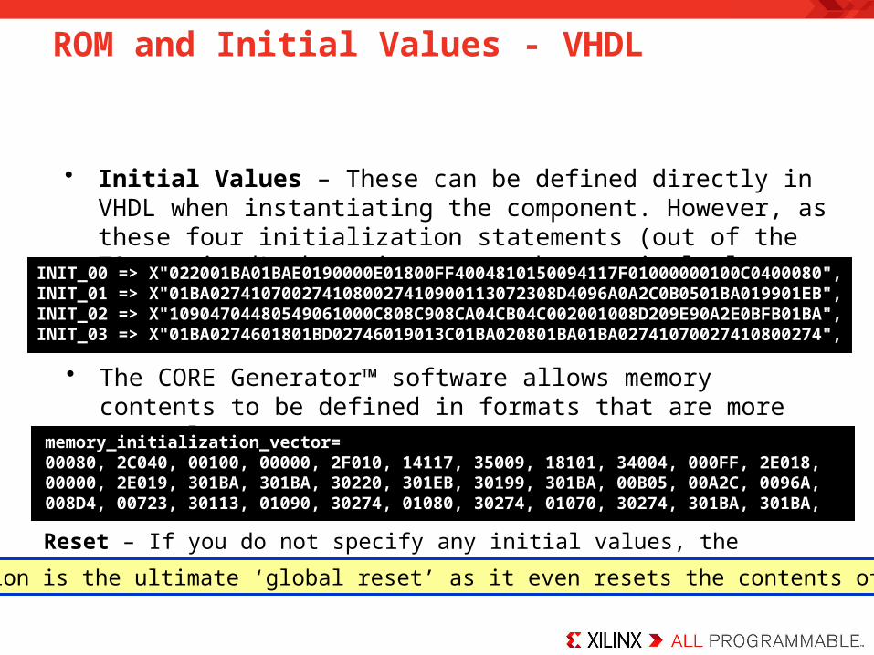
• Initial Values – These can be defined directly in VHDL when instantiating the component. However, as these four initialization statements (out of the 72 required) show, it may not be particularly user friendly to design this way
Reset – If you do not specify any initial values, the tools will default to initial contents of zero
• The CORE Generator™ software allows memory contents to be defined in formats that are more natural
memory_initialization_vector=00080, 2C040, 00100, 00000, 2F010, 14117, 35009, 18101, 34004, 000FF, 2E018,00000, 2E019, 301BA, 301BA, 30220, 301EB, 30199, 301BA, 00B05, 00A2C, 0096A,008D4, 00723, 30113, 01090, 30274, 01080, 30274, 01070, 30274, 301BA, 301BA,
INIT_00 => X"022001BA01BAE0190000E01800FF4004810150094117F01000000100C0400080",INIT_01 => X"01BA0274107002741080027410900113072308D4096A0A2C0B0501BA019901EB",INIT_02 => X"10904704480549061000C808C908CA04CB04C002001008D209E90A2E0BFB01BA",INIT_03 => X"01BA0274601801BD02746019013C01BA020801BA01BA02741070027410800274",
Tip: Configuration is the ultimate ‘global reset’ as it even resets the contents of block RAM
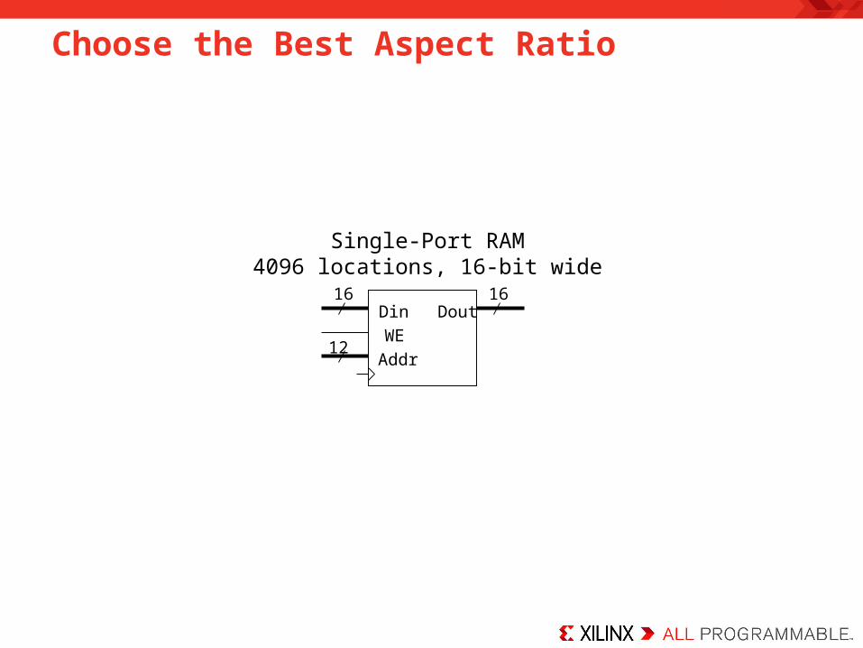
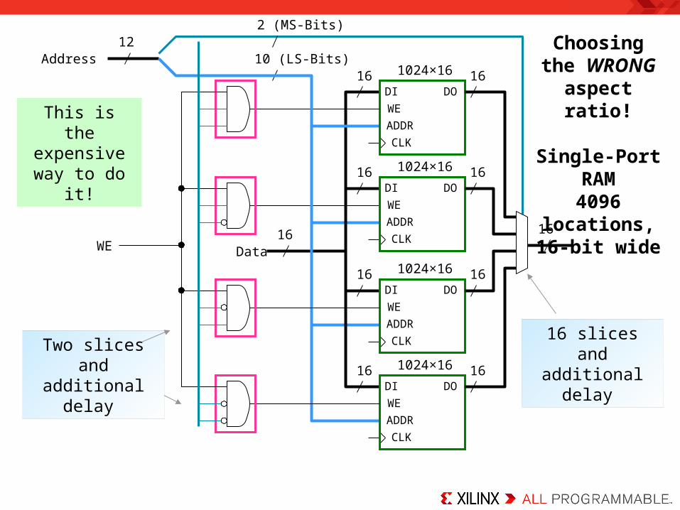
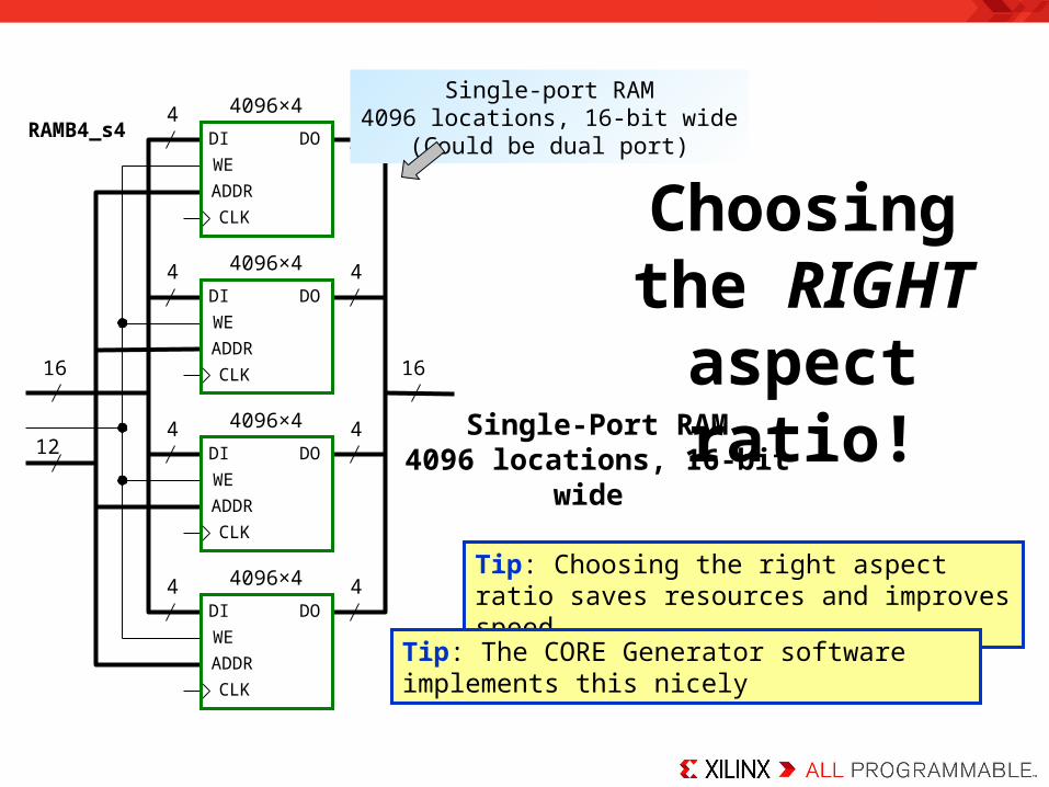
Choose the Best Aspect Ratio
Single-Port RAM4096 locations, 16-bit wide
Din Dout16 16
WEAddr
12
16
CLK
DI
ADDR
DOWE
16
16 16
CLK
DI
ADDR
DOWE
16 16
1024×16
1024×16
CLK
DI
ADDR
DOWE
16 16
CLK
DI
ADDR
DOWE
16 16
1024×16
1024×16
This is the expensive way to
do it!
16 slices and additional delay
Data
Address12
2 (MS-Bits)
10 (LS-Bits)
WE
Two slices and additional delay
Choosing the WRONG aspect
ratio!
Single-Port RAM4096 locations,
16-bit wide
16
12
CLK
DI
ADDR
DOWE
16
4 4
CLK
DI
ADDR
DOWE
4 4
4096×4
4096×4
CLK
DI
ADDR
DOWE
4 4
CLK
DI
ADDR
DOWE
4 4
4096×4
4096×4
RAMB4_s4
Single-port RAM4096 locations, 16-bit wide
(Could be dual port)
Choosing the RIGHT
aspect ratio!Single-Port RAM
4096 locations, 16-bit wide
Tip: Choosing the right aspect ratio saves resources and improves speed
Tip: The CORE Generator software implements this nicely
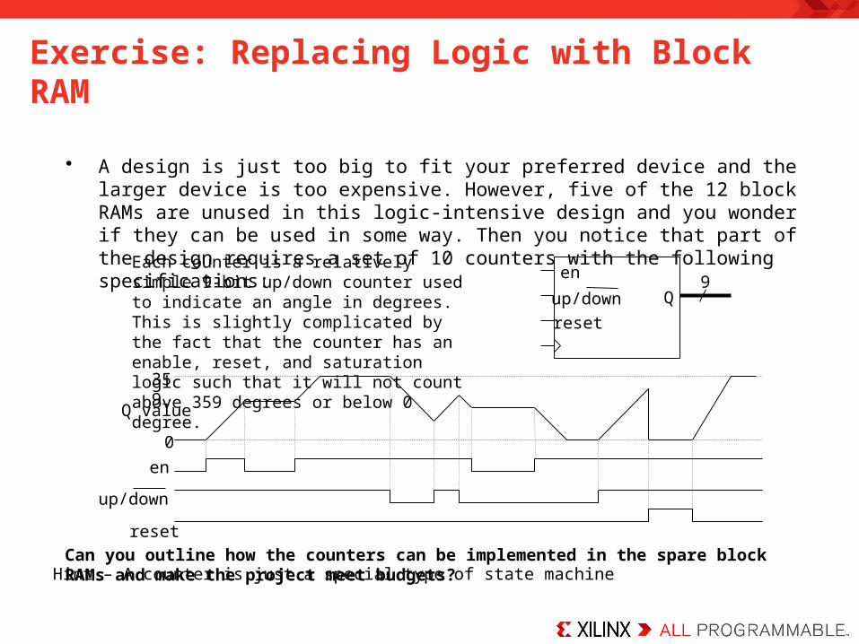
Exercise: Replacing Logic with Block RAM
• A design is just too big to fit your preferred device and the larger device is too expensive. However, five of the 12 block RAMs are unused in this logic-intensive design and you wonder if they can be used in some way. Then you notice that part of the design requires a set of 10 counters with the following specifications:
Can you outline how the counters can be implemented in the spare block RAMs and make the project meet budgets?
Q9
up/downreset
Each counter is a relatively simple 9-bit up/down counter used to indicate an angle in degrees. This is slightly complicated by the fact that the counter has an enable, reset, and saturation logic such that it will not count above 359 degrees or below 0 degree.
en
Q value
359
0
reset
en
up/down
Hint – A counter is just a special type of state machine
8DOA
DOPA 9Q
reseten ENA
SSRA
up / down 11
CLKA
ADDRA
WEA
9
8DOB
DOPB 9Q
reseten ENB
SSRB
up / down 11
CLKB
ADDRB
WEB
9
Addr Data
000 000
SSR Initial value = 000
200
CountDown
CountUp
001
366 167
367 167
001 000
167 166
Hold zero
Hold 359
168
XXX
1FF
368
XXX
7FF
Aspect Ratio2048×9
Hex Table
LUT required if reset to have priority over enable
Tips
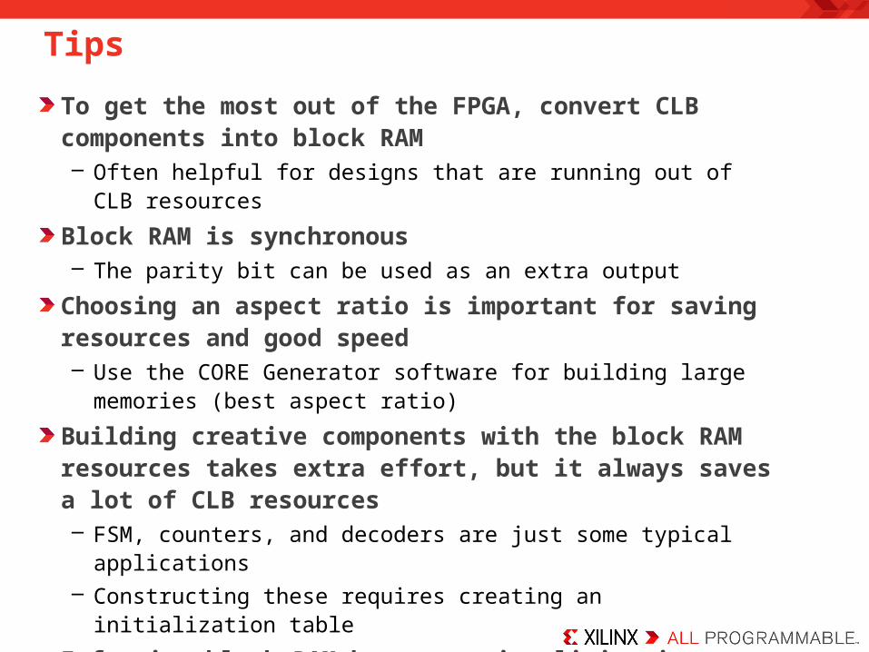
To get the most out of the FPGA, convert CLB components into block RAM– Often helpful for designs that are running out of CLB resources
Block RAM is synchronous– The parity bit can be used as an extra output
Choosing an aspect ratio is important for saving resources and good speed– Use the CORE Generator software for building large memories (best
aspect ratio)
Building creative components with the block RAM resources takes extra effort, but it always saves a lot of CLB resources– FSM, counters, and decoders are just some typical applications– Constructing these requires creating an initialization table
Inferring block RAM has extensive limitations– Most designers use the CORE Generator software
Summary
Take advantage of the IOB resources available to you– Register all I/O– Remember that you waste what you do not use
Minimize the number of clocks in your design– We discussed why to avoid ripple counters
Use case statements to build decode logic– This simplifies the decoding, save LUTs, and improves speed
Avoid global resets– If you cannot avoid global asynchronous resets, be aware that also using
local synchronous resets will end up using more LUTs– Local synchronous reset creates a high fanout net (that might create timing
problems) when there is also a global asynchronous reset
Summary
Take advantage of carry logic when building decoders– Requires you to build with arithmetic rather than logic, but it will run faster
Be aware of the number of inputs to your LUTs when you build with a lot of control signals– We used the loadable up/down counter as a good example
Use the best aspect ratio when building block RAM from scratch– The CORE Generator software does anticipates this automatically
To get the most out of the FPGA, convert CLB components into block RAM– Use block RAM for FSMs, counters, decode logic, and combinatorial
functions, for example

Where Can I Learn More?
Xilinx Online Documents – support.xilinx.com
• To search for an Application Note or White Paper, click the Documentation tab and enter the document number (WP231 or XAPP215) in the search window
• White papers for reference WP275 – Get your Priorities Right – Make your Design Up to 50%
Smaller WP272 – Get Smart About Reset: Think Local, Not Global
• Xilinx Unified Library Guide From the ISE Design Suite, click on the Help menu select Software
Manuals • Block Memory Generator Data Sheet v2.7 (DS512)
Start the Core Generator and start to customize the block RAM, click Help
This data sheet will explain all there is to know about how to build a block RAM memory
Additional Online Training– www.xilinx.com/training

Xilinx is disclosing this Document and Intellectual Property (hereinafter “the Design”) to you for use in the development of designs to operate on, or interface with Xilinx FPGAs. Except as stated herein, none of the Design may be copied, reproduced, distributed, republished, downloaded, displayed, posted, or transmitted in any form or by any means including, but not limited to, electronic, mechanical, photocopying, recording, or otherwise, without the prior written consent of Xilinx. Any unauthorized use of the Design may violate copyright laws, trademark laws, the laws of privacy and publicity, and communications regulations and statutes.
Xilinx does not assume any liability arising out of the application or use of the Design; nor does Xilinx convey any license under its patents, copyrights, or any rights of others. You are responsible for obtaining any rights you may require for your use or implementation of the Design. Xilinx reserves the right to make changes, at any time, to the Design as deemed desirable in the sole discretion of Xilinx. Xilinx assumes no obligation to correct any errors contained herein or to advise you of any correction if such be made. Xilinx will not assume any liability for the accuracy or correctness of any engineering or technical support or assistance provided to you in connection with the Design.
THE DESIGN IS PROVIDED “AS IS" WITH ALL FAULTS, AND THE ENTIRE RISK AS TO ITS FUNCTION AND IMPLEMENTATION IS WITH YOU. YOU ACKNOWLEDGE AND AGREE THAT YOU HAVE NOT RELIED ON ANY ORAL OR WRITTEN INFORMATION OR ADVICE, WHETHER GIVEN BY XILINX, OR ITS AGENTS OR EMPLOYEES. XILINX MAKES NO OTHER WARRANTIES, WHETHER EXPRESS, IMPLIED, OR STATUTORY, REGARDING THE DESIGN, INCLUDING ANY WARRANTIES OF MERCHANTABILITY, FITNESS FOR A PARTICULAR PURPOSE, TITLE, AND NONINFRINGEMENT OF THIRD-PARTY RIGHTS.
IN NO EVENT WILL XILINX BE LIABLE FOR ANY CONSEQUENTIAL, INDIRECT, EXEMPLARY, SPECIAL, OR INCIDENTAL DAMAGES, INCLUDING ANY LOST DATA AND LOST PROFITS, ARISING FROM OR RELATING TO YOUR USE OF THE DESIGN, EVEN IF YOU HAVE BEEN ADVISED OF THE POSSIBILITY OF SUCH DAMAGES. THE TOTAL CUMULATIVE LIABILITY OF XILINX IN CONNECTION WITH YOUR USE OF THE DESIGN, WHETHER IN CONTRACT OR TORT OR OTHERWISE, WILL IN NO EVENT EXCEED THE AMOUNT OF FEES PAID BY YOU TO XILINX HEREUNDER FOR USE OF THE DESIGN. YOU ACKNOWLEDGE THAT THE FEES, IF ANY, REFLECT THE ALLOCATION OF RISK SET FORTH IN THIS AGREEMENT AND THAT XILINX WOULD NOT MAKE AVAILABLE THE DESIGN TO YOU WITHOUT THESE LIMITATIONS OF LIABILITY.
The Design is not designed or intended for use in the development of on-line control equipment in hazardous environments requiring fail-safe controls, such as in the operation of nuclear facilities, aircraft navigation or communications systems, air traffic control, life support, or weapons systems (“High-Risk Applications”). Xilinx specifically disclaims any express or implied warranties of fitness for such High-Risk Applications. You represent that use of the Design in such High-Risk Applications is fully at your risk.
© 2012 Xilinx, Inc. All rights reserved. XILINX, the Xilinx logo, and other designated brands included herein are trademarks of Xilinx, Inc. All other trademarks are the property of their respective owners.
Trademark Information
Related Documents


