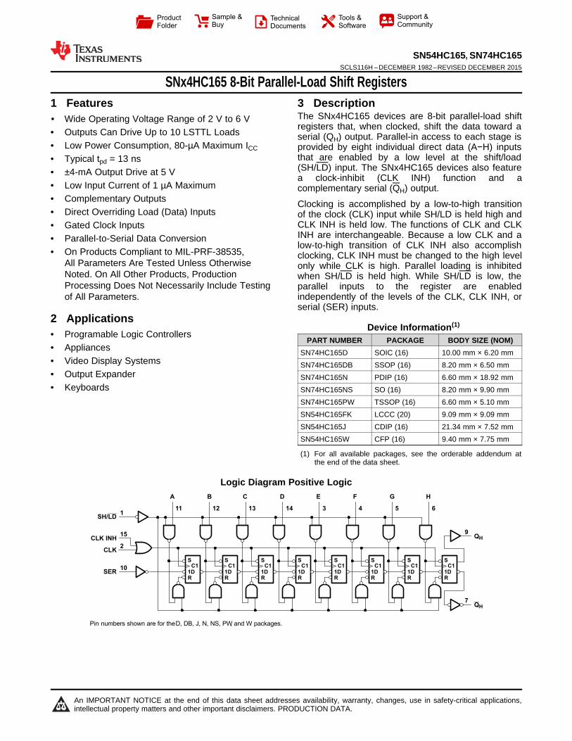
S 1D R C1 S 1D R C1 S 1D R C1 S 1D R C1 S 1D R C1 S 1D R C1 S 1D R C1 S 1D R C1 1 15 2 10 SH/LD CLK INH CLK SER 9 7 Q Q H H 11 12 13 14 3 4 5 6 A B C D E F G H Pin numbers shown are for theD, DB, J, N, NS, PW , and W packages. Product Folder Sample & Buy Technical Documents Tools & Software Support & Community SN54HC165, SN74HC165 SCLS116H – DECEMBER 1982 – REVISED DECEMBER 2015 SNx4HC165 8-Bit Parallel-Load Shift Registers 1 Features 3 Description The SNx4HC165 devices are 8-bit parallel-load shift 1• Wide Operating Voltage Range of 2 V to 6 V registers that, when clocked, shift the data toward a • Outputs Can Drive Up to 10 LSTTL Loads serial (Q H ) output. Parallel-in access to each stage is • Low Power Consumption, 80-μA Maximum I CC provided by eight individual direct data (A−H) inputs that are enabled by a low level at the shift/load • Typical t pd = 13 ns (SH/LD) input. The SNx4HC165 devices also feature • ±4-mA Output Drive at 5 V a clock-inhibit (CLK INH) function and a • Low Input Current of 1 μA Maximum complementary serial (Q H ) output. • Complementary Outputs Clocking is accomplished by a low-to-high transition • Direct Overriding Load (Data) Inputs of the clock (CLK) input while SH/LD is held high and CLK INH is held low. The functions of CLK and CLK • Gated Clock Inputs INH are interchangeable. Because a low CLK and a • Parallel-to-Serial Data Conversion low-to-high transition of CLK INH also accomplish • On Products Compliant to MIL-PRF-38535, clocking, CLK INH must be changed to the high level All Parameters Are Tested Unless Otherwise only while CLK is high. Parallel loading is inhibited Noted. On All Other Products, Production when SH/LD is held high. While SH/LD is low, the Processing Does Not Necessarily Include Testing parallel inputs to the register are enabled independently of the levels of the CLK, CLK INH, or of All Parameters. serial (SER) inputs. 2 Applications Device Information (1) • Programable Logic Controllers PART NUMBER PACKAGE BODY SIZE (NOM) • Appliances SN74HC165D SOIC (16) 10.00 mm × 6.20 mm • Video Display Systems SN74HC165DB SSOP (16) 8.20 mm × 6.50 mm • Output Expander SN74HC165N PDIP (16) 6.60 mm × 18.92 mm • Keyboards SN74HC165NS SO (16) 8.20 mm × 9.90 mm SN74HC165PW TSSOP (16) 6.60 mm × 5.10 mm SN54HC165FK LCCC (20) 9.09 mm × 9.09 mm SN54HC165J CDIP (16) 21.34 mm × 7.52 mm SN54HC165W CFP (16) 9.40 mm × 7.75 mm (1) For all available packages, see the orderable addendum at the end of the data sheet. Logic Diagram Positive Logic 1 An IMPORTANT NOTICE at the end of this data sheet addresses availability, warranty, changes, use in safety-critical applications, intellectual property matters and other important disclaimers. PRODUCTION DATA.

Welcome message from author
This document is posted to help you gain knowledge. Please leave a comment to let me know what you think about it! Share it to your friends and learn new things together.
Transcript
S
1D
R
C1S
1D
R
C1S
1D
R
C1S
1D
R
C1S
1D
R
C1S
1D
R
C1S
1D
R
C1S
1D
R
C1
1
15
2
10
SH/LD
CLK INH
CLK
SER
9
7
Q
Q
H
H
11 12 13 14 3 4 5 6
A B C D E F G H
Pin numbers shown are for theD, DB, J, N, NS, PW, and W packages.
Product
Folder
Sample &Buy
Technical
Documents
Tools &
Software
Support &Community
SN54HC165, SN74HC165SCLS116H –DECEMBER 1982–REVISED DECEMBER 2015
SNx4HC165 8-Bit Parallel-Load Shift Registers1 Features 3 Description
The SNx4HC165 devices are 8-bit parallel-load shift1• Wide Operating Voltage Range of 2 V to 6 V
registers that, when clocked, shift the data toward a• Outputs Can Drive Up to 10 LSTTL Loads serial (QH) output. Parallel-in access to each stage is• Low Power Consumption, 80-µA Maximum ICC provided by eight individual direct data (A−H) inputs
that are enabled by a low level at the shift/load• Typical tpd = 13 ns(SH/LD) input. The SNx4HC165 devices also feature• ±4-mA Output Drive at 5 V a clock-inhibit (CLK INH) function and a
• Low Input Current of 1 µA Maximum complementary serial (QH) output.• Complementary Outputs Clocking is accomplished by a low-to-high transition• Direct Overriding Load (Data) Inputs of the clock (CLK) input while SH/LD is held high and
CLK INH is held low. The functions of CLK and CLK• Gated Clock InputsINH are interchangeable. Because a low CLK and a• Parallel-to-Serial Data Conversionlow-to-high transition of CLK INH also accomplish
• On Products Compliant to MIL-PRF-38535, clocking, CLK INH must be changed to the high levelAll Parameters Are Tested Unless Otherwise only while CLK is high. Parallel loading is inhibitedNoted. On All Other Products, Production when SH/LD is held high. While SH/LD is low, theProcessing Does Not Necessarily Include Testing parallel inputs to the register are enabled
independently of the levels of the CLK, CLK INH, orof All Parameters.serial (SER) inputs.
2 ApplicationsDevice Information(1)
• Programable Logic ControllersPART NUMBER PACKAGE BODY SIZE (NOM)
• Appliances SN74HC165D SOIC (16) 10.00 mm × 6.20 mm• Video Display Systems SN74HC165DB SSOP (16) 8.20 mm × 6.50 mm• Output Expander SN74HC165N PDIP (16) 6.60 mm × 18.92 mm• Keyboards SN74HC165NS SO (16) 8.20 mm × 9.90 mm
SN74HC165PW TSSOP (16) 6.60 mm × 5.10 mmSN54HC165FK LCCC (20) 9.09 mm × 9.09 mmSN54HC165J CDIP (16) 21.34 mm × 7.52 mmSN54HC165W CFP (16) 9.40 mm × 7.75 mm
(1) For all available packages, see the orderable addendum atthe end of the data sheet.
Logic Diagram Positive Logic
1
An IMPORTANT NOTICE at the end of this data sheet addresses availability, warranty, changes, use in safety-critical applications,intellectual property matters and other important disclaimers. PRODUCTION DATA.
SN54HC165, SN74HC165SCLS116H –DECEMBER 1982–REVISED DECEMBER 2015 www.ti.com
Table of Contents1 Features .................................................................. 1 7 Parameter Measurement Information ................ 112 Applications ........................................................... 1 8 Detailed Description ............................................ 12
8.1 Overview ................................................................. 123 Description ............................................................. 18.2 Functional Block Diagram ....................................... 124 Revision History..................................................... 28.3 Feature Description................................................. 135 Pin Configuration and Functions ......................... 38.4 Device Functional Table ......................................... 136 Specifications......................................................... 4
9 Application and Implementation ........................ 146.1 Absolute Maximum Ratings ...................................... 49.1 Application Information............................................ 146.2 ESD Ratings ............................................................ 49.2 Typical Application ................................................. 146.3 Recommended Operating Conditions....................... 4
10 Power Supply Recommendations ..................... 156.4 Thermal Information .................................................. 411 Layout................................................................... 156.5 Electrical Characteristics, TA = 25°C ........................ 5
11.1 Layout Guidelines ................................................. 156.6 Electrical Characteristics, SN54HC165 .................... 511.2 Layout Example .................................................... 156.7 Electrical Characteristics, SN74HC165 .................... 5
6.8 Switching Characteristics, TA = 25°C........................ 6 12 Device and Documentation Support ................. 166.9 Switching Characteristics, SN54HC165.................... 6 12.1 Documentation Support ........................................ 166.10 Switching Characteristics, SN74HC165.................. 7 12.2 Related Links ........................................................ 166.11 Timing Requirements, TA = 25°C............................ 7 12.3 Community Resources.......................................... 166.12 Timing Requirements, SN54HC165........................ 8 12.4 Trademarks ........................................................... 166.13 Timing Requirements, SN74HC165 ....................... 9 12.5 Electrostatic Discharge Caution............................ 166.14 Operating Characteristics...................................... 10 12.6 Glossary ................................................................ 166.15 Typical Characteristics .......................................... 11 13 Mechanical, Packaging, and Orderable
Information ........................................................... 16
4 Revision HistoryNOTE: Page numbers for previous revisions may differ from page numbers in the current version.
Changes from Revision G (August 2013) to Revision H Page
• Added Applications section, Device Information table, Pin Configuration and Functions section, ESD Ratings table,Feature Description section, Device Functional Modes, Application and Implementation section, Power SupplyRecommendations section, Layout section, Device and Documentation Support section, and Mechanical,Packaging, and Orderable Information section ..................................................................................................................... 1
• Added Military Disclaimer to Features list. ............................................................................................................................. 1• Added ESD warning. ............................................................................................................................................................ 16
Changes from Revision F (December 2010) to Revision G Page
• Updated document to new TI data sheet format - no specification changes. ........................................................................ 1• Removed Ordering Information table. .................................................................................................................................... 1• Added Handling Ratings table. ............................................................................................................................................... 4• Extended maximum temperature operating range from 85°C to 125°C................................................................................. 4
2 Submit Documentation Feedback Copyright © 1982–2015, Texas Instruments Incorporated
Product Folder Links: SN54HC165 SN74HC165
3 2 1 20 19
9 10 11 12 13
4
5
6
7
8
18
17
16
15
14
D
C
NC
B
A
E
F
NC
G
H
CLK
SH
/LD
NC
SE
RC
LK
INH
H
GN
D
NC
VC
C
Q
HQ
1
2
3
4
5
6
7
8
16
15
14
13
12
11
10
9
SH/LD
CLK
E
F
G
H
QH
GND
VCC
CLK INH
D
C
B
A
SER
QH
SN54HC165, SN74HC165www.ti.com SCLS116H –DECEMBER 1982–REVISED DECEMBER 2015
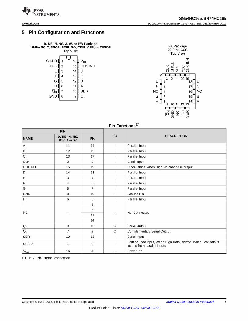
5 Pin Configuration and Functions
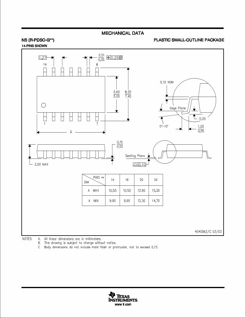
D, DB, N, NS, J, W, or PW PackageFK Package16-Pin SOIC, SSOP, PDIP, SO, CDIP, CFP, or TSSOP20-Pin LCCCTop View
Top View
Pin Functions (1)
PINI/O DESCRIPTIOND, DB, N, NS,NAME FKPW, J or W
A 11 14 I Parallel InputB 12 15 I Parallel InputC 13 17 I Parallel InputCLK 2 3 I Clock inputCLK INH 15 19 I Clock Inhibit, when High No change in outputD 14 18 I Parallel InputE 3 4 I Parallel InputF 4 5 I Parallel InputG 5 7 I Parallel InputGND 8 10 — Ground PinH 6 8 I Parallel Input
16
NC — — Not Connected1116
QH 9 12 O Serial OutputQH 7 9 O Complementary Serial OutputSER 10 13 I Serial Input
Shift or Load input, When High Data, shifted. When Low data isSH/LD 1 2 I loaded from parallel inputsVCC 16 20 — Power Pin
(1) NC – No internal connection
Copyright © 1982–2015, Texas Instruments Incorporated Submit Documentation Feedback 3
Product Folder Links: SN54HC165 SN74HC165
SN54HC165, SN74HC165SCLS116H –DECEMBER 1982–REVISED DECEMBER 2015 www.ti.com
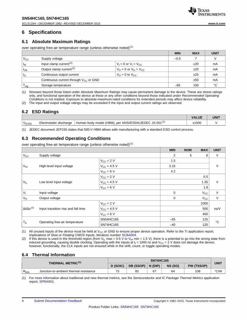
6 Specifications
6.1 Absolute Maximum Ratingsover operating free-air temperature range (unless otherwise noted) (1)
MIN MAX UNITVCC Supply voltage –0.5 7 VIIK Input clamp current (2) VI < 0 or VI > VCC ±20 mAIOK Output clamp current (2) VO < 0 or VO > VCC ±20 mAIO Continuous output current VO = 0 to VCC ±25 mA
Continuous current through VCC or GND ±50 mATstg Storage temperature –65 150 °C
(1) Stresses beyond those listed under Absolute Maximum Ratings may cause permanent damage to the device. These are stress ratingsonly, and functional operation of the device at these or any other conditions beyond those indicated under Recommended OperatingConditions is not implied. Exposure to absolute-maximum-rated conditions for extended periods may affect device reliability.
(2) The input and output voltage ratings may be exceeded if the input and output current ratings are observed.
6.2 ESD RatingsVALUE UNIT
V(ESD) Electrostatic discharge Human body model (HBM), per ANSI/ESDA/JEDEC JS-001 (1) ±1500 V
(1) JEDEC document JEP155 states that 500-V HBM allows safe manufacturing with a standard ESD control process.
6.3 Recommended Operating Conditionsover operating free-air temperature range (unless otherwise noted) (1)
MIN NOM MAX UNITVCC Supply voltage 2 5 6 V
VCC = 2 V 1.5VIH High-level input voltage VCC = 4.5 V 3.15 V
VCC = 6 V 4.2VCC = 2 V 0.5
VIL Low level input voltage VCC = 4.5 V 1.35 VVCC = 6 V 1.8
VI Input voltage 0 VCC VVO Output voltage 0 VCC V
VCC = 2 V 1000Δt/Δv (2) Input transition rise and fall time VCC = 4.5 V 500 ns/V
VCC = 6 V 400SN54HC165 –55 125
TA Operating free-air temperature °CSN74HC165 –40 125
(1) All unused inputs of the device must be held at VCC or GND to ensure proper device operation. Refer to the TI application report,Implications of Slow or Floating CMOS Inputs, literature number SCBA004.
(2) If this device is used in the threshold region (from VIL max = 0.5 V to VIH min = 1.5 V), there is a potential to go into the wrong state frominduced grounding, causing double clocking. Operating with the inputs at tt = 1000 ns and VCC = 2 V does not damage the device;however, functionally, the CLK inputs are not ensured while in the shift, count, or toggle operating modes.
6.4 Thermal InformationSN74HC165
THERMAL METRIC (1) UNITD (SOIC) DB (SSOP) N (DIP) NS (SO) PW (TSSOP)
RθJA Junction-to-ambient thermal resistance 73 82 67 64 108 °C/W
(1) For more information about traditional and new thermal metrics, see the Semiconductor and IC Package Thermal Metrics applicationreport, SPRA953.
4 Submit Documentation Feedback Copyright © 1982–2015, Texas Instruments Incorporated
Product Folder Links: SN54HC165 SN74HC165
SN54HC165, SN74HC165www.ti.com SCLS116H –DECEMBER 1982–REVISED DECEMBER 2015
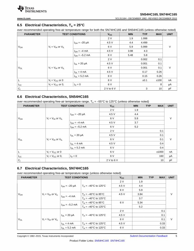
6.5 Electrical Characteristics, TA = 25°Cover recommended operating free-air temperature range for both the SN74HC165 and SN54HC165 (unless otherwise noted)
PARAMETER TEST CONDITIONS VCC MIN TYP MAX UNIT2 V 1.9 1.998
IOH = –20 µA 4.5 V 4.4 4.499VOH VI = VIH or VIL 6 V 5.9 5.999 V
IOH = –4 mA 4.5 V 3.98 4.3IOH = –5.2 mA 6 V 5.48 5.8
2 V 0.002 0.1IOL = 20 µA 4.5 V 0.001 0.1
VOL VI = VIH or VIL 6 V 0.001 0.1 VIOL = 4 mA 4.5 V 0.17 0.26IOL = 5.2 mA 6 V 0.15 0.26
II VI = VCC or 0 6 V ±0.1 ±100 nAICC VI = VCC or 0, IO = 0 6 V 8 µACi 2 V to 6 V 3 10 pF
6.6 Electrical Characteristics, SN54HC165over recommended operating free-air temperature range, TA = –55°C to 125°C (unless otherwise noted)
PARAMETER TEST CONDITIONS VCC MIN TYP MAX UNIT2 V 1.9
IOH = –20 µA 4.5 V 4.4VOH VI = VIH or VIL 6 V 5.9 V
IOH = –4 mA 4.5 V 3.7IOH = –5.2 mA 6 V 5.2
2 V 0.1IOL = 20 µA 4.5 V 0.1
VOL VI = VIH or VIL 6 V 0.1 VIOL = 4 mA 4.5 V 0.4IOL = 5.2 mA 6 V 0.4
II VI = VCC or 0 6 V ±1000 nAICC VI = VCC or 0, IO = 0 6 V 160 µACi 2 V to 6 V 10 pF
6.7 Electrical Characteristics, SN74HC165over recommended operating free-air temperature range (unless otherwise noted)
PARAMETER TEST CONDITIONS VCC MIN TYP MAX UNIT2 V 1.9
IOH = –20 µA TA = –40°C to 125°C 4.5 V 4.46 V 5.9
VOH VI = VIH or VIL TA = –40°C to 85°C 4.5 V 3.84 VIOH = –4 mA
TA = –40°C to 125°C 3.7TA = –40°C to 85°C 6 V 5.34
IOH = –5.2 mATA = –40°C to 125°C 5.2
2 V 0.1IOL = 20 µA TA = –40°C to 125°C 4.5 V 0.1
VOL VI = VIH or VIL 6 V 0.1 VIOL = 4 mA TA = –40°C to 125°C 4.5 V 0.33IOL = 5.2 mA TA = –40°C to 125°C 6 V 0.33
Copyright © 1982–2015, Texas Instruments Incorporated Submit Documentation Feedback 5
Product Folder Links: SN54HC165 SN74HC165
SN54HC165, SN74HC165SCLS116H –DECEMBER 1982–REVISED DECEMBER 2015 www.ti.com
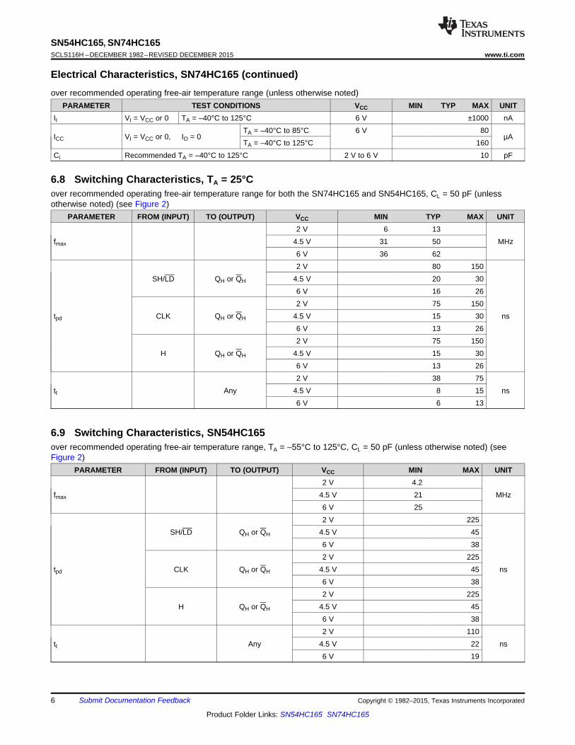
Electrical Characteristics, SN74HC165 (continued)over recommended operating free-air temperature range (unless otherwise noted)
PARAMETER TEST CONDITIONS VCC MIN TYP MAX UNITII VI = VCC or 0 TA = –40°C to 125°C 6 V ±1000 nA
TA = –40°C to 85°C 6 V 80ICC VI = VCC or 0, IO = 0 µA
TA = –40°C to 125°C 160Ci Recommended TA = –40°C to 125°C 2 V to 6 V 10 pF
6.8 Switching Characteristics, TA = 25°Cover recommended operating free-air temperature range for both the SN74HC165 and SN54HC165, CL = 50 pF (unlessotherwise noted) (see Figure 2)
PARAMETER FROM (INPUT) TO (OUTPUT) VCC MIN TYP MAX UNIT2 V 6 13
fmax 4.5 V 31 50 MHz6 V 36 622 V 80 150
SH/LD QH or QH 4.5 V 20 306 V 16 262 V 75 150
tpd CLK QH or QH 4.5 V 15 30 ns6 V 13 262 V 75 150
H QH or QH 4.5 V 15 306 V 13 262 V 38 75
tt Any 4.5 V 8 15 ns6 V 6 13
6.9 Switching Characteristics, SN54HC165over recommended operating free-air temperature range, TA = –55°C to 125°C, CL = 50 pF (unless otherwise noted) (seeFigure 2)
PARAMETER FROM (INPUT) TO (OUTPUT) VCC MIN MAX UNIT2 V 4.2
fmax 4.5 V 21 MHz6 V 252 V 225
SH/LD QH or QH 4.5 V 456 V 382 V 225
tpd CLK QH or QH 4.5 V 45 ns6 V 382 V 225
H QH or QH 4.5 V 456 V 382 V 110
tt Any 4.5 V 22 ns6 V 19
6 Submit Documentation Feedback Copyright © 1982–2015, Texas Instruments Incorporated
Product Folder Links: SN54HC165 SN74HC165
SN54HC165, SN74HC165www.ti.com SCLS116H –DECEMBER 1982–REVISED DECEMBER 2015
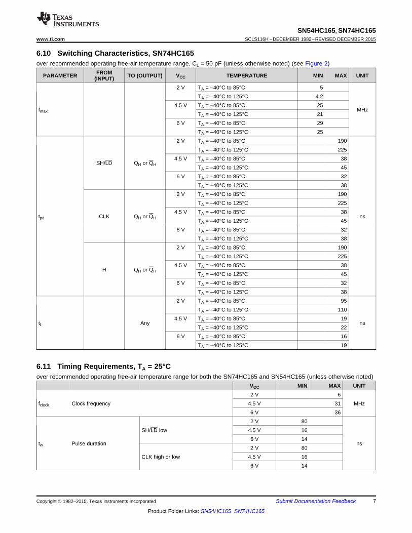
6.10 Switching Characteristics, SN74HC165over recommended operating free-air temperature range, CL = 50 pF (unless otherwise noted) (see Figure 2)
FROMPARAMETER TO (OUTPUT) VCC TEMPERATURE MIN MAX UNIT(INPUT)2 V TA = –40°C to 85°C 5
TA = –40°C to 125°C 4.24.5 V TA = –40°C to 85°C 25
fmax MHzTA = –40°C to 125°C 21
6 V TA = –40°C to 85°C 29TA = –40°C to 125°C 25
2 V TA = –40°C to 85°C 190TA = –40°C to 125°C 225
4.5 V TA = –40°C to 85°C 38SH/LD QH or QH TA = –40°C to 125°C 45
6 V TA = –40°C to 85°C 32TA = –40°C to 125°C 38
2 V TA = –40°C to 85°C 190TA = –40°C to 125°C 225
4.5 V TA = –40°C to 85°C 38tpd CLK QH or QH ns
TA = –40°C to 125°C 456 V TA = –40°C to 85°C 32
TA = –40°C to 125°C 382 V TA = –40°C to 85°C 190
TA = –40°C to 125°C 2254.5 V TA = –40°C to 85°C 38
H QH or QH TA = –40°C to 125°C 456 V TA = –40°C to 85°C 32
TA = –40°C to 125°C 382 V TA = –40°C to 85°C 95
TA = –40°C to 125°C 1104.5 V TA = –40°C to 85°C 19
tt Any nsTA = –40°C to 125°C 22
6 V TA = –40°C to 85°C 16TA = –40°C to 125°C 19
6.11 Timing Requirements, TA = 25°Cover recommended operating free-air temperature range for both the SN74HC165 and SN54HC165 (unless otherwise noted)
VCC MIN MAX UNIT2 V 6
fclock Clock frequency 4.5 V 31 MHz6 V 362 V 80
SH/LD low 4.5 V 166 V 14
tw Pulse duration ns2 V 80
CLK high or low 4.5 V 166 V 14
Copyright © 1982–2015, Texas Instruments Incorporated Submit Documentation Feedback 7
Product Folder Links: SN54HC165 SN74HC165
SN54HC165, SN74HC165SCLS116H –DECEMBER 1982–REVISED DECEMBER 2015 www.ti.com
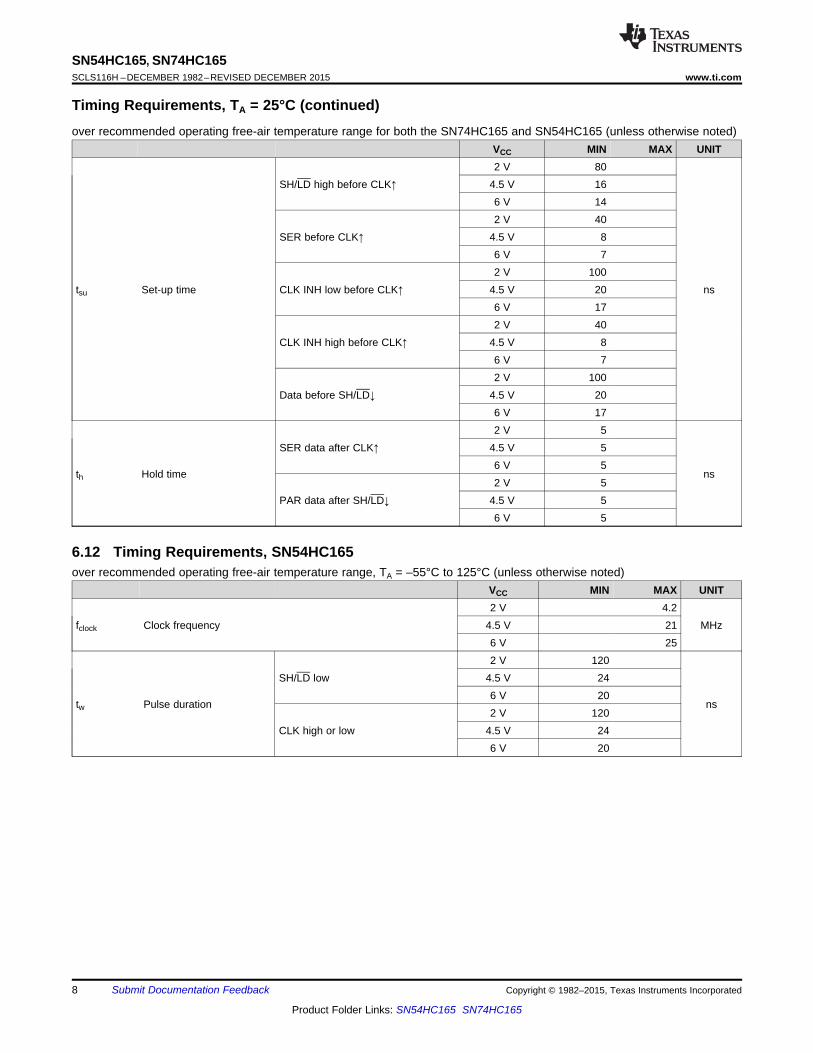
Timing Requirements, TA = 25°C (continued)over recommended operating free-air temperature range for both the SN74HC165 and SN54HC165 (unless otherwise noted)
VCC MIN MAX UNIT2 V 80
SH/LD high before CLK↑ 4.5 V 166 V 142 V 40
SER before CLK↑ 4.5 V 86 V 72 V 100
tsu Set-up time CLK INH low before CLK↑ 4.5 V 20 ns6 V 172 V 40
CLK INH high before CLK↑ 4.5 V 86 V 72 V 100
Data before SH/LD↓ 4.5 V 206 V 172 V 5
SER data after CLK↑ 4.5 V 56 V 5
th Hold time ns2 V 5
PAR data after SH/LD↓ 4.5 V 56 V 5
6.12 Timing Requirements, SN54HC165over recommended operating free-air temperature range, TA = –55°C to 125°C (unless otherwise noted)
VCC MIN MAX UNIT2 V 4.2
fclock Clock frequency 4.5 V 21 MHz6 V 252 V 120
SH/LD low 4.5 V 246 V 20
tw Pulse duration ns2 V 120
CLK high or low 4.5 V 246 V 20
8 Submit Documentation Feedback Copyright © 1982–2015, Texas Instruments Incorporated
Product Folder Links: SN54HC165 SN74HC165
SN54HC165, SN74HC165www.ti.com SCLS116H –DECEMBER 1982–REVISED DECEMBER 2015
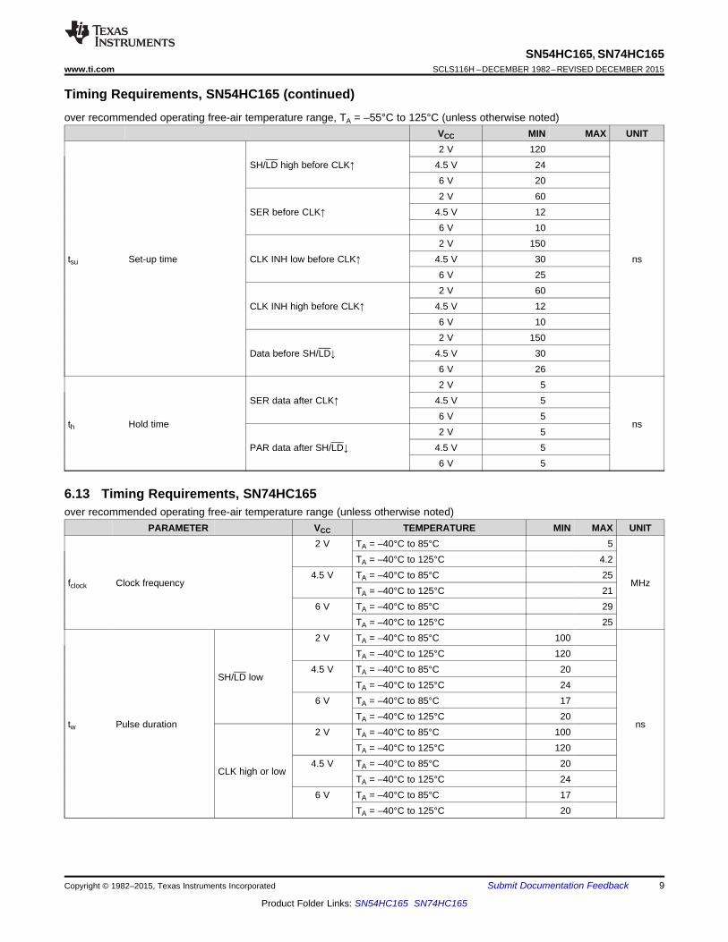
Timing Requirements, SN54HC165 (continued)over recommended operating free-air temperature range, TA = –55°C to 125°C (unless otherwise noted)
VCC MIN MAX UNIT2 V 120
SH/LD high before CLK↑ 4.5 V 246 V 202 V 60
SER before CLK↑ 4.5 V 126 V 102 V 150
tsu Set-up time CLK INH low before CLK↑ 4.5 V 30 ns6 V 252 V 60
CLK INH high before CLK↑ 4.5 V 126 V 102 V 150
Data before SH/LD↓ 4.5 V 306 V 262 V 5
SER data after CLK↑ 4.5 V 56 V 5
th Hold time ns2 V 5
PAR data after SH/LD↓ 4.5 V 56 V 5
6.13 Timing Requirements, SN74HC165over recommended operating free-air temperature range (unless otherwise noted)
PARAMETER VCC TEMPERATURE MIN MAX UNIT2 V TA = –40°C to 85°C 5
TA = –40°C to 125°C 4.24.5 V TA = –40°C to 85°C 25
fclock Clock frequency MHzTA = –40°C to 125°C 21
6 V TA = –40°C to 85°C 29TA = –40°C to 125°C 25
2 V TA = –40°C to 85°C 100TA = –40°C to 125°C 120
4.5 V TA = –40°C to 85°C 20SH/LD low
TA = –40°C to 125°C 246 V TA = –40°C to 85°C 17
TA = –40°C to 125°C 20tw Pulse duration ns
2 V TA = –40°C to 85°C 100TA = –40°C to 125°C 120
4.5 V TA = –40°C to 85°C 20CLK high or low
TA = –40°C to 125°C 246 V TA = –40°C to 85°C 17
TA = –40°C to 125°C 20
Copyright © 1982–2015, Texas Instruments Incorporated Submit Documentation Feedback 9
Product Folder Links: SN54HC165 SN74HC165
SN54HC165, SN74HC165SCLS116H –DECEMBER 1982–REVISED DECEMBER 2015 www.ti.com
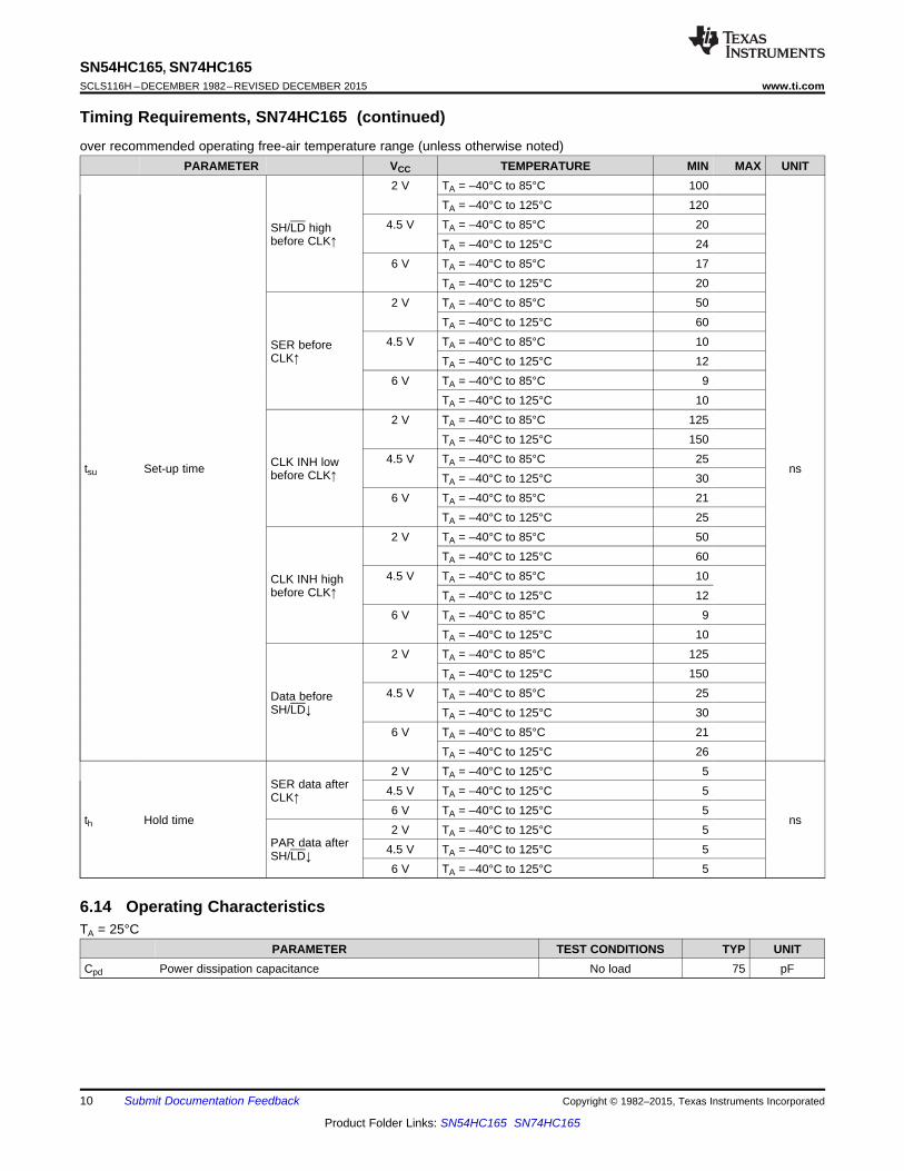
Timing Requirements, SN74HC165 (continued)over recommended operating free-air temperature range (unless otherwise noted)
PARAMETER VCC TEMPERATURE MIN MAX UNIT2 V TA = –40°C to 85°C 100
TA = –40°C to 125°C 1204.5 V TA = –40°C to 85°C 20SH/LD high
before CLK↑ TA = –40°C to 125°C 246 V TA = –40°C to 85°C 17
TA = –40°C to 125°C 202 V TA = –40°C to 85°C 50
TA = –40°C to 125°C 604.5 V TA = –40°C to 85°C 10SER before
CLK↑ TA = –40°C to 125°C 126 V TA = –40°C to 85°C 9
TA = –40°C to 125°C 102 V TA = –40°C to 85°C 125
TA = –40°C to 125°C 1504.5 V TA = –40°C to 85°C 25CLK INH lowtsu Set-up time nsbefore CLK↑ TA = –40°C to 125°C 306 V TA = –40°C to 85°C 21
TA = –40°C to 125°C 252 V TA = –40°C to 85°C 50
TA = –40°C to 125°C 604.5 V TA = –40°C to 85°C 10CLK INH high
before CLK↑ TA = –40°C to 125°C 126 V TA = –40°C to 85°C 9
TA = –40°C to 125°C 102 V TA = –40°C to 85°C 125
TA = –40°C to 125°C 1504.5 V TA = –40°C to 85°C 25Data before
SH/LD↓ TA = –40°C to 125°C 306 V TA = –40°C to 85°C 21
TA = –40°C to 125°C 262 V TA = –40°C to 125°C 5
SER data after 4.5 V TA = –40°C to 125°C 5CLK↑6 V TA = –40°C to 125°C 5
th Hold time ns2 V TA = –40°C to 125°C 5
PAR data after 4.5 V TA = –40°C to 125°C 5SH/LD↓6 V TA = –40°C to 125°C 5
6.14 Operating CharacteristicsTA = 25°C
PARAMETER TEST CONDITIONS TYP UNITCpd Power dissipation capacitance No load 75 pF
10 Submit Documentation Feedback Copyright © 1982–2015, Texas Instruments Incorporated
Product Folder Links: SN54HC165 SN74HC165
VOLTAGE WAVEFORMS
SETUP AND HOLD AND INPUT RISE AND FALL TIMES
VOLTAGE WAVEFORMS
PULSE DURATIONS
thtsu
50%
50%50%10%10%
90% 90%
VCC
VCC
0 V
0 V
tr t
Reference
f
Input
Data
Input
50%High-Level
Pulse50%
VCC
0 V
50% 50%
VCC
0 V
t
Low-Level
w
Pulse
VOLTAGE WAVEFORMS
PROPAGATION DELAY AND OUTPUT TRANSITION TIMES
50%
50%50%10%10%
90% 90%
VCC
VOH
VOL
0 V
tr t
Input
f
In-Phase
Output
50%
tPLH tPHL
50% 50%10% 10%
90%90%VOH
VOL
tt rf
tPHL tPLH
Out-of-Phase
Output
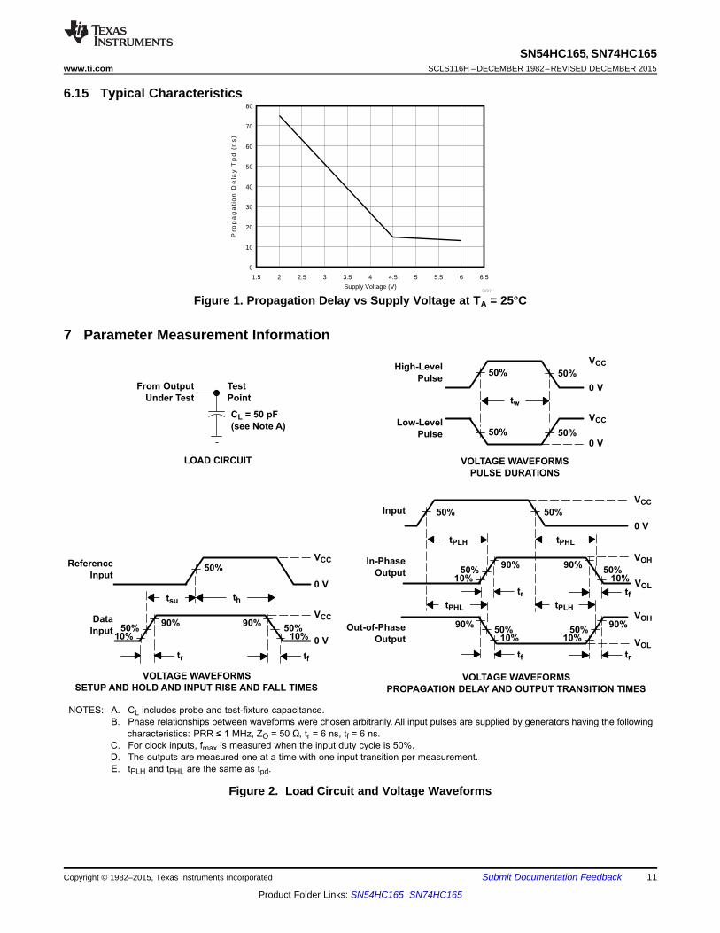
NOTES: A. CL includes probe and test-fixture capacitance.
B. Phase relationships between waveforms were chosen arbitrarily. All input pulses are supplied by generators having the following
characteristics: PRR ≤ 1 MHz, ZO = 50 Ω, tr = 6 ns, tf = 6 ns.
C. For clock inputs, fmax is measured when the input duty cycle is 50%.
D. The outputs are measured one at a time with one input transition per measurement.
E. tPLH and tPHL are the same as tpd.
Test
Point
From Output
Under Test
CL = 50 pF
(see Note A)
LOAD CIRCUIT
Supply Voltage (V)
Pro
pa
ga
tio
n D
ela
y T
pd
(n
s)
1.5 2 2.5 3 3.5 4 4.5 5 5.5 6 6.5
0
10
20
30
40
50
60
70
80
D001
SN54HC165, SN74HC165www.ti.com SCLS116H –DECEMBER 1982–REVISED DECEMBER 2015
6.15 Typical Characteristics
Figure 1. Propagation Delay vs Supply Voltage at TA = 25°C
7 Parameter Measurement Information
Figure 2. Load Circuit and Voltage Waveforms
Copyright © 1982–2015, Texas Instruments Incorporated Submit Documentation Feedback 11
Product Folder Links: SN54HC165 SN74HC165
Load
E
QH
H
G
C
F
Data
Inputs
D
SH/LD
SER
CLK INH
CLK
B
A
Q
L
H
L
H
L
H
L
H
H
H
H
L
H
L
H
L
H
L
H
L
L
H
L
H
L
H
Inhibit Serial Shift
S
1D
R
C1S
1D
R
C1S
1D
R
C1S
1D
R
C1S
1D
R
C1S
1D
R
C1S
1D
R
C1S
1D
R
C1
1
15
2
10
SH/LD
CLK INH
CLK
SER
9
7
Q
Q
H
H
11 12 13 14 3 4 5 6
A B C D E F G H
Pin numbers shown are for theD, DB, J, N, NS, PW, and W packages.
SN54HC165, SN74HC165SCLS116H –DECEMBER 1982–REVISED DECEMBER 2015 www.ti.com
8 Detailed Description
8.1 OverviewThe SNx4HC165 is an 8-bit Parallel load shift register with 1 serial input and 8 parallel load input. The deviceloads all the 8 bits simultaneously through parallel load input when SH/LD is low. This will also ignore any inputat CLK or CLK INH.
The device shifts the data when CLK toggles. The data is shifted on rising edge of the clock. Clock Inhibit (CLKINH) inhibits the clock function resulting in no change of the output. If SH/LD is low clock inputs are ignored. Torealize the shift function, SH/LD should be high.
CLK and CLK INH functions are interchangeable. If CLK is low then change a clock signal at CLK INH pincauses a shift of data to QH. If CLK INH is Low clock signal on CLK pin shifts the data out to QH.
8.2 Functional Block Diagram
Figure 3. Logic Diagram Positive Logic
Figure 4. Typical Shift, Load, and Inhibit Sequence
12 Submit Documentation Feedback Copyright © 1982–2015, Texas Instruments Incorporated
Product Folder Links: SN54HC165 SN74HC165
SN54HC165, SN74HC165www.ti.com SCLS116H –DECEMBER 1982–REVISED DECEMBER 2015
8.3 Feature DescriptionThe SNx4HC165 has a wide operating voltage range of 2 V to 6 V, outputs that can drive up to 10 LSTTL loadsand Low Power Consumption, 80-μA maximum I. It is typically tpd = 13 ns and has ±4-mA output drive at 5 V withlow input current of 1-μA maximum. The device features the direct overloading load of data input, meaningparallel data is loaded irrespective of clock signals.
8.4 Device Functional TableTable 1 lists the functional modes of the SNx4HC165.
Table 1. Function TableINPUTS
FUNCTIONSH/LD CLK CLK INH
L X X Parallel loadH H X No changeH X H No changeH L ↑ Shift (1)
H ↑ L Shift (1)
(1) Shift : Content of each internal register shifts towards serial output QH. Data at SER is shifted into the first register
Copyright © 1982–2015, Texas Instruments Incorporated Submit Documentation Feedback 13
Product Folder Links: SN54HC165 SN74HC165
12
9
7
13
3
11
Controller,
Processor
14
4
5
VCC
6
16
0.1 µF
Digital
Inputs /
Keyboard
Da
ta
8
2
15
12
9
7
13
3
11
14
4
5
VCC
6
16
0.1µFD
ata
8
2
15
10
Digital
Inputs /
Keyboard
1110From other shift register
SN54HC165, SN74HC165SCLS116H –DECEMBER 1982–REVISED DECEMBER 2015 www.ti.com
9 Application and Implementation
NOTEInformation in the following applications sections is not part of the TI componentspecification, and TI does not warrant its accuracy or completeness. TI’s customers areresponsible for determining suitability of components for their purposes. Customers shouldvalidate and test their design implementation to confirm system functionality.
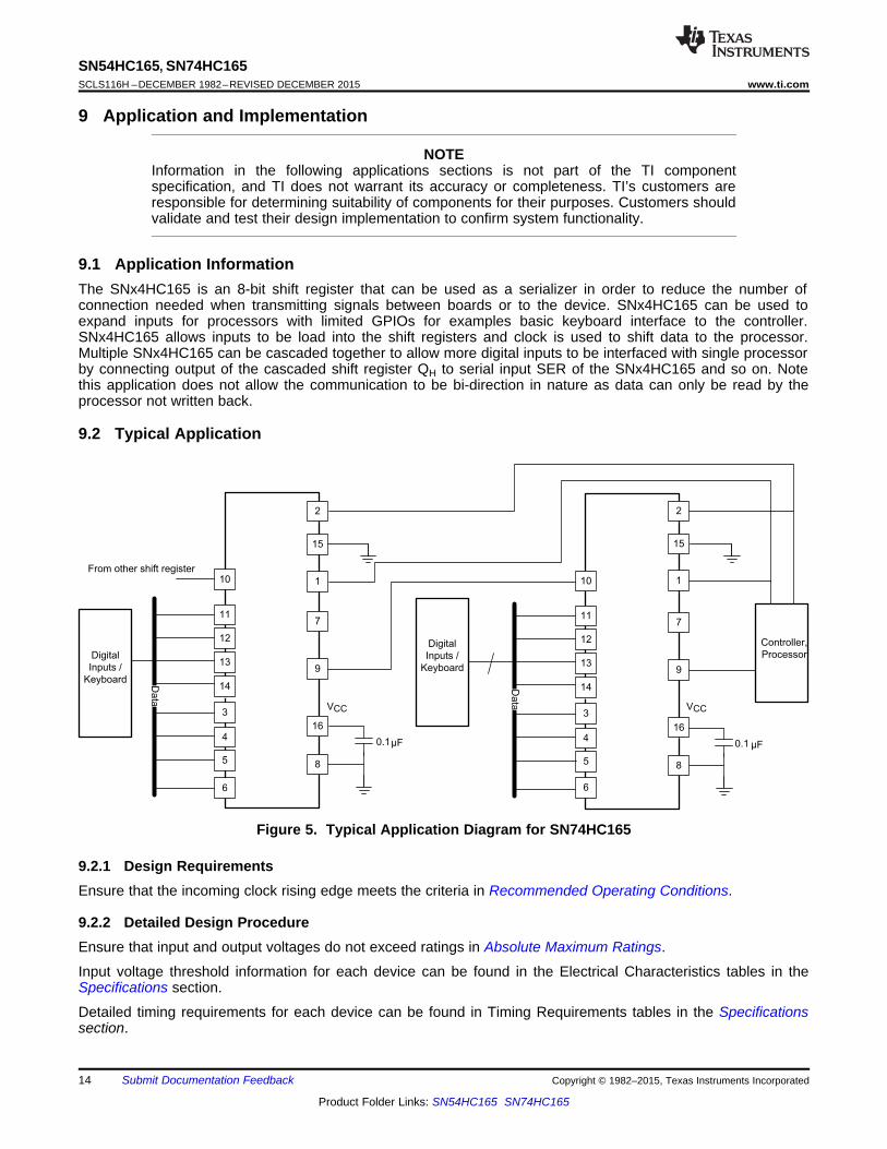
9.1 Application InformationThe SNx4HC165 is an 8-bit shift register that can be used as a serializer in order to reduce the number ofconnection needed when transmitting signals between boards or to the device. SNx4HC165 can be used toexpand inputs for processors with limited GPIOs for examples basic keyboard interface to the controller.SNx4HC165 allows inputs to be load into the shift registers and clock is used to shift data to the processor.Multiple SNx4HC165 can be cascaded together to allow more digital inputs to be interfaced with single processorby connecting output of the cascaded shift register QH to serial input SER of the SNx4HC165 and so on. Notethis application does not allow the communication to be bi-direction in nature as data can only be read by theprocessor not written back.
9.2 Typical Application
Figure 5. Typical Application Diagram for SN74HC165
9.2.1 Design RequirementsEnsure that the incoming clock rising edge meets the criteria in Recommended Operating Conditions.
9.2.2 Detailed Design ProcedureEnsure that input and output voltages do not exceed ratings in Absolute Maximum Ratings.
Input voltage threshold information for each device can be found in the Electrical Characteristics tables in theSpecifications section.
Detailed timing requirements for each device can be found in Timing Requirements tables in the Specificationssection.
14 Submit Documentation Feedback Copyright © 1982–2015, Texas Instruments Incorporated
Product Folder Links: SN54HC165 SN74HC165
WORST BETTER BEST
1W min.
W
2W
Supply Voltage (V)
Pro
pa
ga
tio
n D
ela
y T
pd
(n
s)
1.5 2 2.5 3 3.5 4 4.5 5 5.5 6 6.5
0
10
20
30
40
50
60
70
80
D001
SN54HC165, SN74HC165www.ti.com SCLS116H –DECEMBER 1982–REVISED DECEMBER 2015
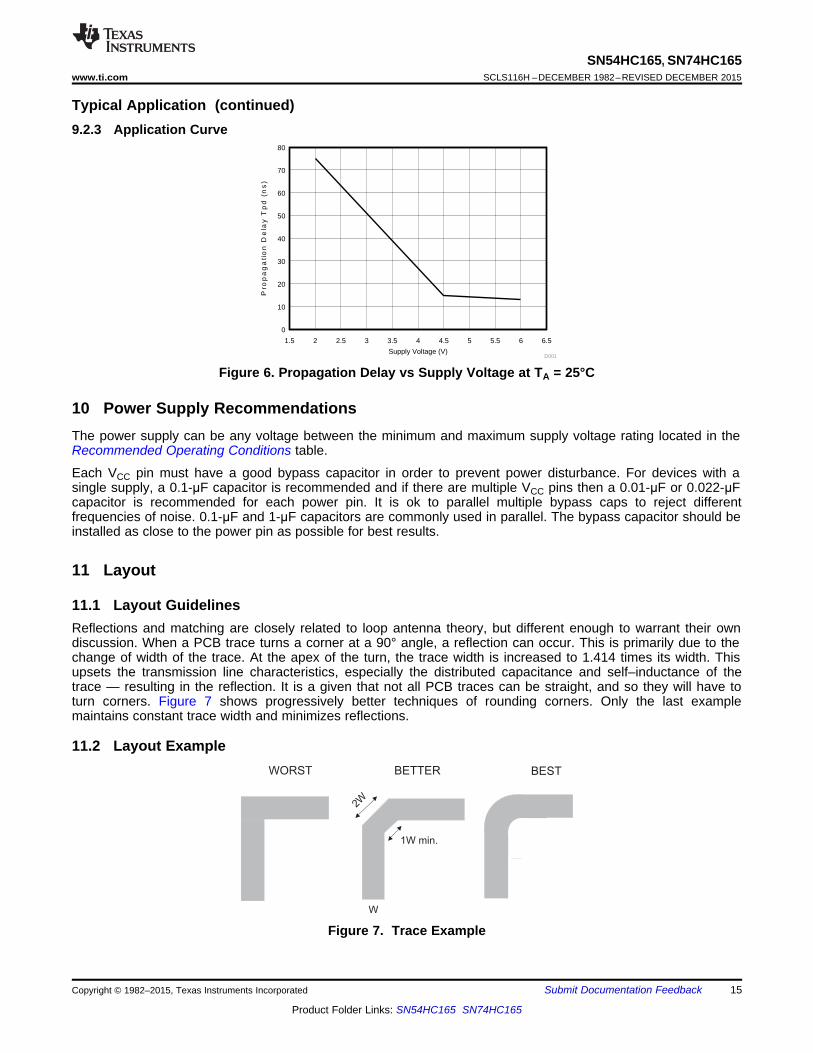
Typical Application (continued)9.2.3 Application Curve
Figure 6. Propagation Delay vs Supply Voltage at TA = 25°C
10 Power Supply RecommendationsThe power supply can be any voltage between the minimum and maximum supply voltage rating located in theRecommended Operating Conditions table.
Each VCC pin must have a good bypass capacitor in order to prevent power disturbance. For devices with asingle supply, a 0.1-μF capacitor is recommended and if there are multiple VCC pins then a 0.01-μF or 0.022-μFcapacitor is recommended for each power pin. It is ok to parallel multiple bypass caps to reject differentfrequencies of noise. 0.1-μF and 1-μF capacitors are commonly used in parallel. The bypass capacitor should beinstalled as close to the power pin as possible for best results.
11 Layout
11.1 Layout GuidelinesReflections and matching are closely related to loop antenna theory, but different enough to warrant their owndiscussion. When a PCB trace turns a corner at a 90° angle, a reflection can occur. This is primarily due to thechange of width of the trace. At the apex of the turn, the trace width is increased to 1.414 times its width. Thisupsets the transmission line characteristics, especially the distributed capacitance and self–inductance of thetrace — resulting in the reflection. It is a given that not all PCB traces can be straight, and so they will have toturn corners. Figure 7 shows progressively better techniques of rounding corners. Only the last examplemaintains constant trace width and minimizes reflections.
11.2 Layout Example
Figure 7. Trace Example
Copyright © 1982–2015, Texas Instruments Incorporated Submit Documentation Feedback 15
Product Folder Links: SN54HC165 SN74HC165
SN54HC165, SN74HC165SCLS116H –DECEMBER 1982–REVISED DECEMBER 2015 www.ti.com
12 Device and Documentation Support
12.1 Documentation Support
12.1.1 Related DocumentationImplications of Slow or Floating CMOS Inputs, SCBA004.
12.2 Related LinksThe table below lists quick access links. Categories include technical documents, support and communityresources, tools and software, and quick access to sample or buy.
Table 2. Related LinksTECHNICAL TOOLS & SUPPORT &PARTS PRODUCT FOLDER SAMPLE & BUY DOCUMENTS SOFTWARE COMMUNITY
SN54HC165 Click here Click here Click here Click here Click hereSN74HC165 Click here Click here Click here Click here Click here
12.3 Community ResourcesThe following links connect to TI community resources. Linked contents are provided "AS IS" by the respectivecontributors. They do not constitute TI specifications and do not necessarily reflect TI's views; see TI's Terms ofUse.
TI E2E™ Online Community TI's Engineer-to-Engineer (E2E) Community. Created to foster collaborationamong engineers. At e2e.ti.com, you can ask questions, share knowledge, explore ideas and helpsolve problems with fellow engineers.
Design Support TI's Design Support Quickly find helpful E2E forums along with design support tools andcontact information for technical support.
12.4 TrademarksE2E is a trademark of Texas Instruments.All other trademarks are the property of their respective owners.
12.5 Electrostatic Discharge CautionThese devices have limited built-in ESD protection. The leads should be shorted together or the device placed in conductive foamduring storage or handling to prevent electrostatic damage to the MOS gates.
12.6 GlossarySLYZ022 — TI Glossary.
This glossary lists and explains terms, acronyms and definitions.
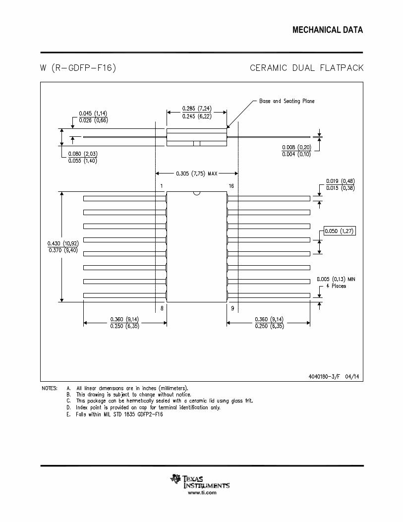
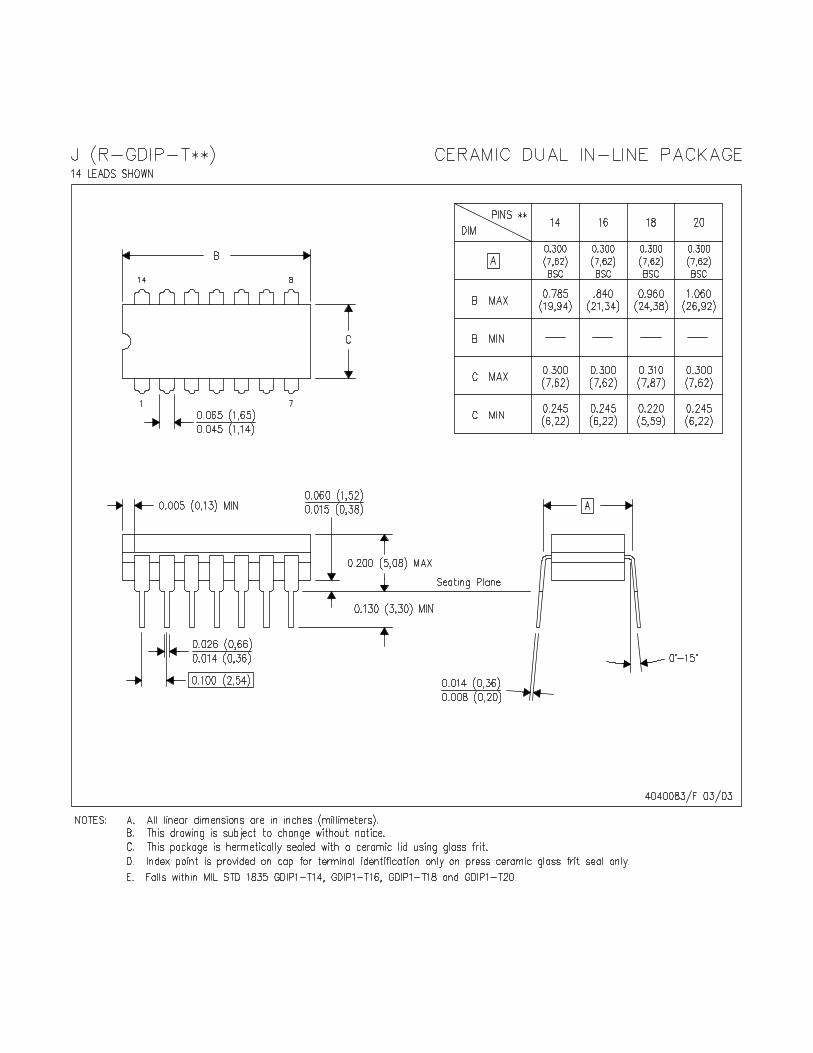
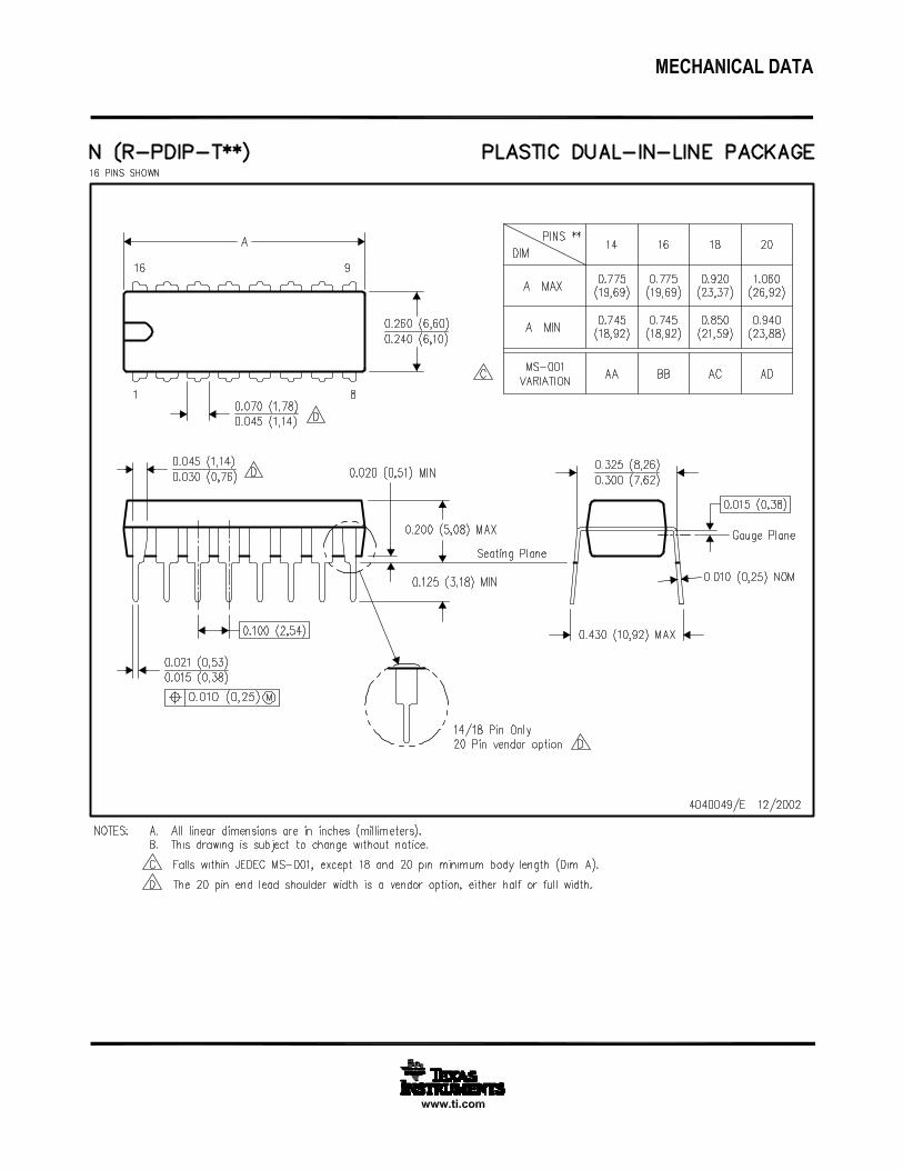
13 Mechanical, Packaging, and Orderable InformationThe following pages include mechanical packaging and orderable information. This information is the mostcurrent data available for the designated devices. This data is subject to change without notice and revision ofthis document. For browser based versions of this data sheet, refer to the left hand navigation.
16 Submit Documentation Feedback Copyright © 1982–2015, Texas Instruments Incorporated
Product Folder Links: SN54HC165 SN74HC165
PACKAGE OPTION ADDENDUM
www.ti.com 16-Dec-2021
Addendum-Page 1
PACKAGING INFORMATION
Orderable Device Status(1)
Package Type PackageDrawing
Pins PackageQty
Eco Plan(2)
Lead finish/Ball material
(6)
MSL Peak Temp(3)
Op Temp (°C) Device Marking(4/5)
Samples
84095012A ACTIVE LCCC FK 20 1 Non-RoHS& Green
SNPB N / A for Pkg Type -55 to 125 84095012ASNJ54HC165FK
8409501EA ACTIVE CDIP J 16 1 Non-RoHS& Green
SNPB N / A for Pkg Type -55 to 125 8409501EASNJ54HC165J
8409501FA ACTIVE CFP W 16 1 Non-RoHS& Green
SNPB N / A for Pkg Type -55 to 125 8409501FASNJ54HC165W
SN54HC165J ACTIVE CDIP J 16 1 Non-RoHS& Green
SNPB N / A for Pkg Type -55 to 125 SN54HC165J
SN74HC165D ACTIVE SOIC D 16 40 RoHS & Green NIPDAU Level-1-260C-UNLIM -40 to 125 HC165
SN74HC165DBR ACTIVE SSOP DB 16 2000 RoHS & Green NIPDAU Level-1-260C-UNLIM -40 to 125 HC165
SN74HC165DE4 ACTIVE SOIC D 16 40 RoHS & Green NIPDAU Level-1-260C-UNLIM -40 to 125 HC165
SN74HC165DG4 ACTIVE SOIC D 16 40 RoHS & Green NIPDAU Level-1-260C-UNLIM -40 to 125 HC165
SN74HC165DR ACTIVE SOIC D 16 2500 RoHS & Green NIPDAU | SN Level-1-260C-UNLIM -40 to 125 HC165
SN74HC165DRE4 ACTIVE SOIC D 16 2500 RoHS & Green NIPDAU Level-1-260C-UNLIM -40 to 125 HC165
SN74HC165DRG3 ACTIVE SOIC D 16 2500 RoHS & Green SN Level-1-260C-UNLIM -40 to 125 HC165
SN74HC165DRG4 ACTIVE SOIC D 16 2500 RoHS & Green NIPDAU Level-1-260C-UNLIM -40 to 125 HC165
SN74HC165DT ACTIVE SOIC D 16 250 RoHS & Green NIPDAU Level-1-260C-UNLIM -40 to 125 HC165
SN74HC165N ACTIVE PDIP N 16 25 RoHS & Green NIPDAU | SN N / A for Pkg Type -40 to 125 SN74HC165N
SN74HC165NE4 ACTIVE PDIP N 16 25 RoHS & Green NIPDAU N / A for Pkg Type -40 to 125 SN74HC165N
SN74HC165NSR ACTIVE SO NS 16 2000 RoHS & Green NIPDAU Level-1-260C-UNLIM -40 to 125 HC165
SN74HC165PW ACTIVE TSSOP PW 16 90 RoHS & Green NIPDAU Level-1-260C-UNLIM -40 to 125 HC165
SN74HC165PWR ACTIVE TSSOP PW 16 2000 RoHS & Green NIPDAU | SN Level-1-260C-UNLIM -40 to 125 HC165
SN74HC165PWRG3 ACTIVE TSSOP PW 16 2000 RoHS & Green SN Level-1-260C-UNLIM -40 to 125 HC165
PACKAGE OPTION ADDENDUM
www.ti.com 16-Dec-2021
Addendum-Page 2
Orderable Device Status(1)
Package Type PackageDrawing
Pins PackageQty
Eco Plan(2)
Lead finish/Ball material
(6)
MSL Peak Temp(3)
Op Temp (°C) Device Marking(4/5)
Samples
SN74HC165PWRG4 ACTIVE TSSOP PW 16 2000 RoHS & Green NIPDAU Level-1-260C-UNLIM -40 to 125 HC165
SN74HC165PWT ACTIVE TSSOP PW 16 250 RoHS & Green NIPDAU Level-1-260C-UNLIM -40 to 125 HC165
SNJ54HC165FK ACTIVE LCCC FK 20 1 Non-RoHS& Green
SNPB N / A for Pkg Type -55 to 125 84095012ASNJ54HC165FK
SNJ54HC165J ACTIVE CDIP J 16 1 Non-RoHS& Green
SNPB N / A for Pkg Type -55 to 125 8409501EASNJ54HC165J
SNJ54HC165W ACTIVE CFP W 16 1 Non-RoHS& Green
SNPB N / A for Pkg Type -55 to 125 8409501FASNJ54HC165W
(1) The marketing status values are defined as follows:ACTIVE: Product device recommended for new designs.LIFEBUY: TI has announced that the device will be discontinued, and a lifetime-buy period is in effect.NRND: Not recommended for new designs. Device is in production to support existing customers, but TI does not recommend using this part in a new design.PREVIEW: Device has been announced but is not in production. Samples may or may not be available.OBSOLETE: TI has discontinued the production of the device.
(2) RoHS: TI defines "RoHS" to mean semiconductor products that are compliant with the current EU RoHS requirements for all 10 RoHS substances, including the requirement that RoHS substancedo not exceed 0.1% by weight in homogeneous materials. Where designed to be soldered at high temperatures, "RoHS" products are suitable for use in specified lead-free processes. TI mayreference these types of products as "Pb-Free".RoHS Exempt: TI defines "RoHS Exempt" to mean products that contain lead but are compliant with EU RoHS pursuant to a specific EU RoHS exemption.Green: TI defines "Green" to mean the content of Chlorine (Cl) and Bromine (Br) based flame retardants meet JS709B low halogen requirements of <=1000ppm threshold. Antimony trioxide basedflame retardants must also meet the <=1000ppm threshold requirement.
(3) MSL, Peak Temp. - The Moisture Sensitivity Level rating according to the JEDEC industry standard classifications, and peak solder temperature.
(4) There may be additional marking, which relates to the logo, the lot trace code information, or the environmental category on the device.
(5) Multiple Device Markings will be inside parentheses. Only one Device Marking contained in parentheses and separated by a "~" will appear on a device. If a line is indented then it is a continuationof the previous line and the two combined represent the entire Device Marking for that device.
(6) Lead finish/Ball material - Orderable Devices may have multiple material finish options. Finish options are separated by a vertical ruled line. Lead finish/Ball material values may wrap to twolines if the finish value exceeds the maximum column width.
PACKAGE OPTION ADDENDUM
www.ti.com 16-Dec-2021
Addendum-Page 3
Important Information and Disclaimer:The information provided on this page represents TI's knowledge and belief as of the date that it is provided. TI bases its knowledge and belief on informationprovided by third parties, and makes no representation or warranty as to the accuracy of such information. Efforts are underway to better integrate information from third parties. TI has taken andcontinues to take reasonable steps to provide representative and accurate information but may not have conducted destructive testing or chemical analysis on incoming materials and chemicals.TI and TI suppliers consider certain information to be proprietary, and thus CAS numbers and other limited information may not be available for release.
In no event shall TI's liability arising out of such information exceed the total purchase price of the TI part(s) at issue in this document sold by TI to Customer on an annual basis.
OTHER QUALIFIED VERSIONS OF SN54HC165, SN74HC165 :
• Catalog : SN74HC165
• Automotive : SN74HC165-Q1, SN74HC165-Q1
• Enhanced Product : SN74HC165-EP, SN74HC165-EP
• Military : SN54HC165
NOTE: Qualified Version Definitions:
• Catalog - TI's standard catalog product
• Automotive - Q100 devices qualified for high-reliability automotive applications targeting zero defects
• Enhanced Product - Supports Defense, Aerospace and Medical Applications
• Military - QML certified for Military and Defense Applications
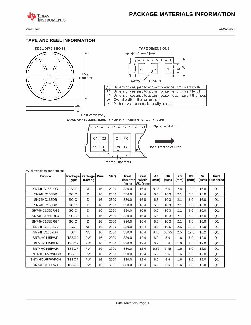
TAPE AND REEL INFORMATION
*All dimensions are nominal
Device PackageType
PackageDrawing
Pins SPQ ReelDiameter
(mm)
ReelWidth
W1 (mm)
A0(mm)
B0(mm)
K0(mm)
P1(mm)
W(mm)
Pin1Quadrant
SN74HC165DBR SSOP DB 16 2000 330.0 16.4 8.35 6.6 2.4 12.0 16.0 Q1
SN74HC165DR SOIC D 16 2500 330.0 16.4 6.5 10.3 2.1 8.0 16.0 Q1
SN74HC165DR SOIC D 16 2500 330.0 16.8 6.5 10.3 2.1 8.0 16.0 Q1
SN74HC165DR SOIC D 16 2500 330.0 16.4 6.5 10.3 2.1 8.0 16.0 Q1
SN74HC165DRG3 SOIC D 16 2500 330.0 16.8 6.5 10.3 2.1 8.0 16.0 Q1
SN74HC165DRG4 SOIC D 16 2500 330.0 16.4 6.5 10.3 2.1 8.0 16.0 Q1
SN74HC165DRG4 SOIC D 16 2500 330.0 16.4 6.5 10.3 2.1 8.0 16.0 Q1
SN74HC165NSR SO NS 16 2000 330.0 16.4 8.2 10.5 2.5 12.0 16.0 Q1
SN74HC165NSR SO NS 16 2000 330.0 16.4 8.45 10.55 2.5 12.0 16.2 Q1
SN74HC165PWR TSSOP PW 16 2000 330.0 12.4 6.9 5.6 1.6 8.0 12.0 Q1
SN74HC165PWR TSSOP PW 16 2000 330.0 12.4 6.9 5.6 1.6 8.0 12.0 Q1
SN74HC165PWR TSSOP PW 16 2000 330.0 12.4 6.85 5.45 1.6 8.0 12.0 Q1
SN74HC165PWRG3 TSSOP PW 16 2000 330.0 12.4 6.9 5.6 1.6 8.0 12.0 Q1
SN74HC165PWRG4 TSSOP PW 16 2000 330.0 12.4 6.9 5.6 1.6 8.0 12.0 Q1
SN74HC165PWT TSSOP PW 16 250 330.0 12.4 6.9 5.6 1.6 8.0 12.0 Q1
PACKAGE MATERIALS INFORMATION
www.ti.com 24-Mar-2022
Pack Materials-Page 1
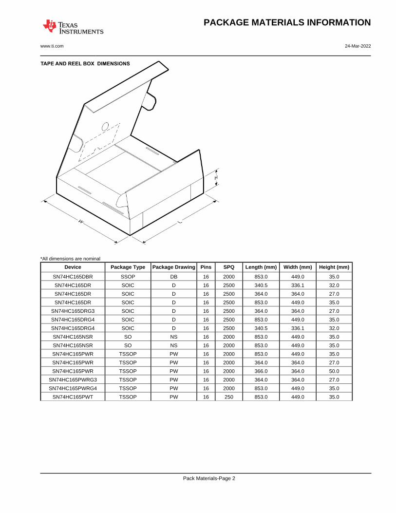
*All dimensions are nominal
Device Package Type Package Drawing Pins SPQ Length (mm) Width (mm) Height (mm)
SN74HC165DBR SSOP DB 16 2000 853.0 449.0 35.0
SN74HC165DR SOIC D 16 2500 340.5 336.1 32.0
SN74HC165DR SOIC D 16 2500 364.0 364.0 27.0
SN74HC165DR SOIC D 16 2500 853.0 449.0 35.0
SN74HC165DRG3 SOIC D 16 2500 364.0 364.0 27.0
SN74HC165DRG4 SOIC D 16 2500 853.0 449.0 35.0
SN74HC165DRG4 SOIC D 16 2500 340.5 336.1 32.0
SN74HC165NSR SO NS 16 2000 853.0 449.0 35.0
SN74HC165NSR SO NS 16 2000 853.0 449.0 35.0
SN74HC165PWR TSSOP PW 16 2000 853.0 449.0 35.0
SN74HC165PWR TSSOP PW 16 2000 364.0 364.0 27.0
SN74HC165PWR TSSOP PW 16 2000 366.0 364.0 50.0
SN74HC165PWRG3 TSSOP PW 16 2000 364.0 364.0 27.0
SN74HC165PWRG4 TSSOP PW 16 2000 853.0 449.0 35.0
SN74HC165PWT TSSOP PW 16 250 853.0 449.0 35.0
PACKAGE MATERIALS INFORMATION
www.ti.com 24-Mar-2022
Pack Materials-Page 2
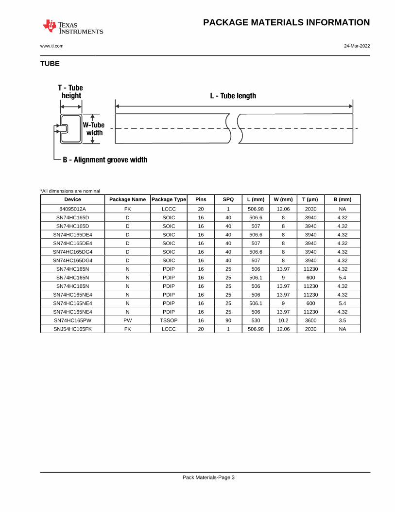
TUBE
*All dimensions are nominal
Device Package Name Package Type Pins SPQ L (mm) W (mm) T (µm) B (mm)
84095012A FK LCCC 20 1 506.98 12.06 2030 NA
SN74HC165D D SOIC 16 40 506.6 8 3940 4.32
SN74HC165D D SOIC 16 40 507 8 3940 4.32
SN74HC165DE4 D SOIC 16 40 506.6 8 3940 4.32
SN74HC165DE4 D SOIC 16 40 507 8 3940 4.32
SN74HC165DG4 D SOIC 16 40 506.6 8 3940 4.32
SN74HC165DG4 D SOIC 16 40 507 8 3940 4.32
SN74HC165N N PDIP 16 25 506 13.97 11230 4.32
SN74HC165N N PDIP 16 25 506.1 9 600 5.4
SN74HC165N N PDIP 16 25 506 13.97 11230 4.32
SN74HC165NE4 N PDIP 16 25 506 13.97 11230 4.32
SN74HC165NE4 N PDIP 16 25 506.1 9 600 5.4
SN74HC165NE4 N PDIP 16 25 506 13.97 11230 4.32
SN74HC165PW PW TSSOP 16 90 530 10.2 3600 3.5
SNJ54HC165FK FK LCCC 20 1 506.98 12.06 2030 NA
PACKAGE MATERIALS INFORMATION
www.ti.com 24-Mar-2022
Pack Materials-Page 3
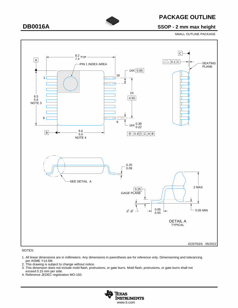
www.ti.com
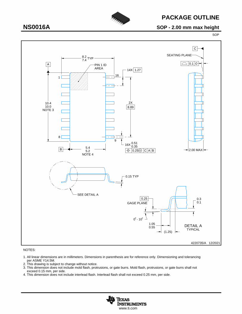
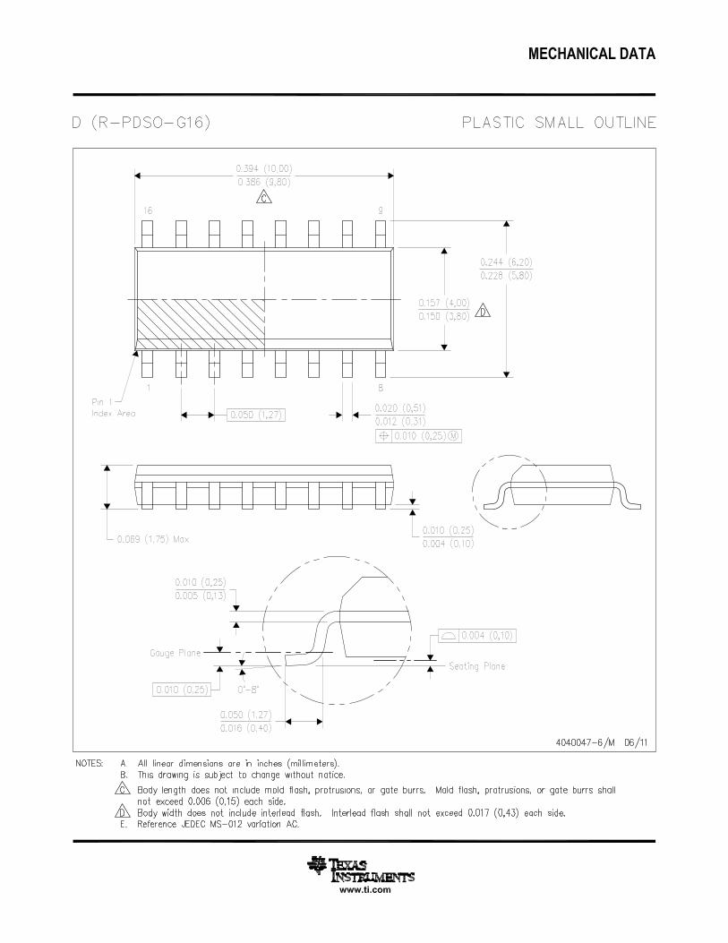
PACKAGE OUTLINE
C
8.27.4 TYP
14X 1.27
16X 0.510.35
2X8.89
0.15 TYP
0 - 10
0.30.1
2.00 MAX
(1.25)
0.25GAGE PLANE
1.050.55
A
10.410.0
NOTE 3
B 5.45.2
NOTE 4
4220735/A 12/2021
SOP - 2.00 mm max heightNS0016ASOP
NOTES: 1. All linear dimensions are in millimeters. Dimensions in parenthesis are for reference only. Dimensioning and tolerancing per ASME Y14.5M. 2. This drawing is subject to change without notice. 3. This dimension does not include mold flash, protrusions, or gate burrs. Mold flash, protrusions, or gate burrs shall not exceed 0.15 mm, per side. 4. This dimension does not include interlead flash. Interlead flash shall not exceed 0.25 mm, per side.
1 16
0.25 C A B
98
PIN 1 IDAREA
SEATING PLANE
0.1 C
SEE DETAIL A
DETAIL ATYPICAL
SCALE 1.500
www.ti.com
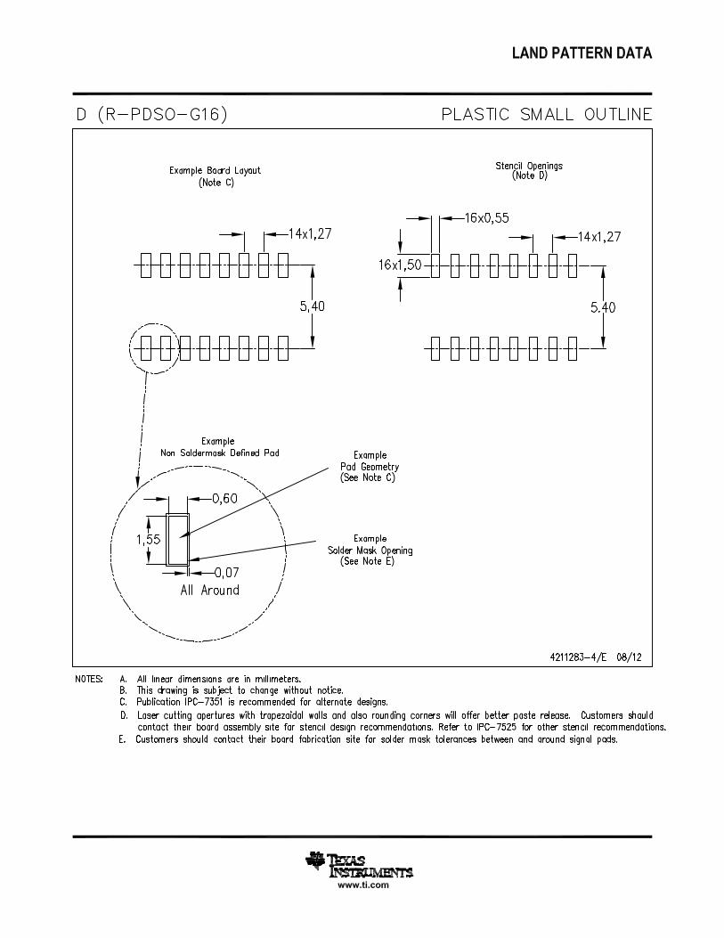
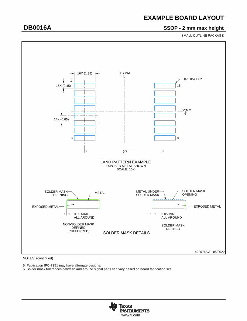
EXAMPLE BOARD LAYOUT
0.07 MAXALL AROUND
0.07 MINALL AROUND
14X (1.27)
(R0.05) TYP
(7)
16X (1.85)
16X (0.6)
4220735/A 12/2021
SOP - 2.00 mm max heightNS0016ASOP
NOTES: (continued) 5. Publication IPC-7351 may have alternate designs. 6. Solder mask tolerances between and around signal pads can vary based on board fabrication site.
METAL SOLDER MASKOPENING
NON SOLDER MASKDEFINED
SOLDER MASK DETAILS
OPENINGSOLDER MASK METAL
SOLDER MASKDEFINED
LAND PATTERN EXAMPLESCALE:7X
SYMM
1
8 9
16
SEEDETAILS
SYMM
www.ti.com
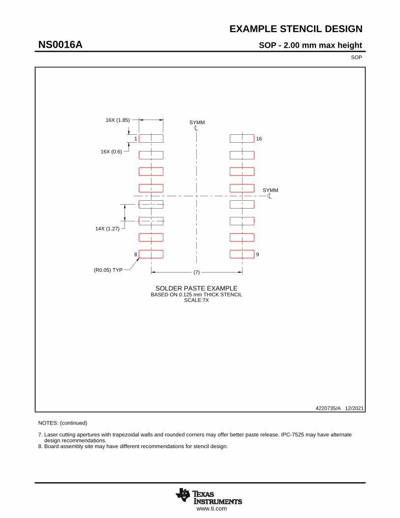
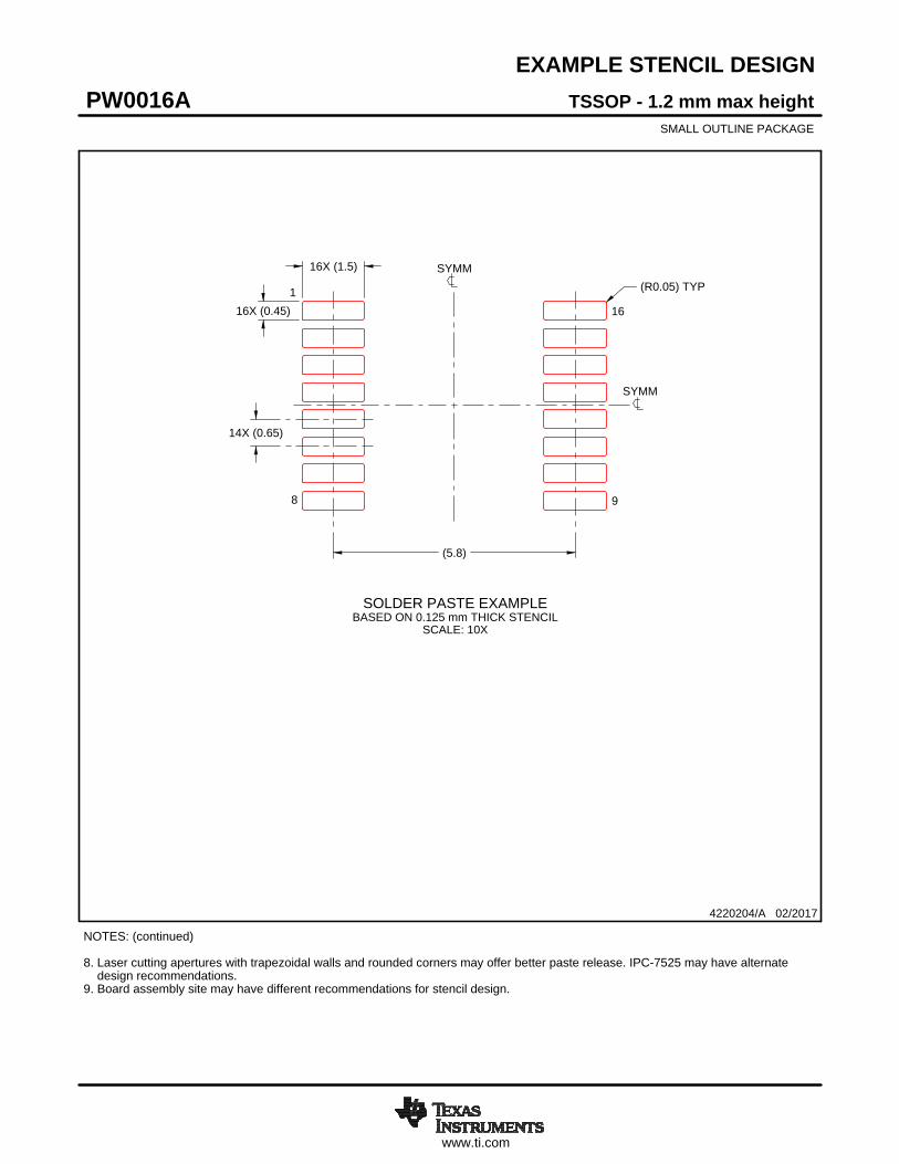
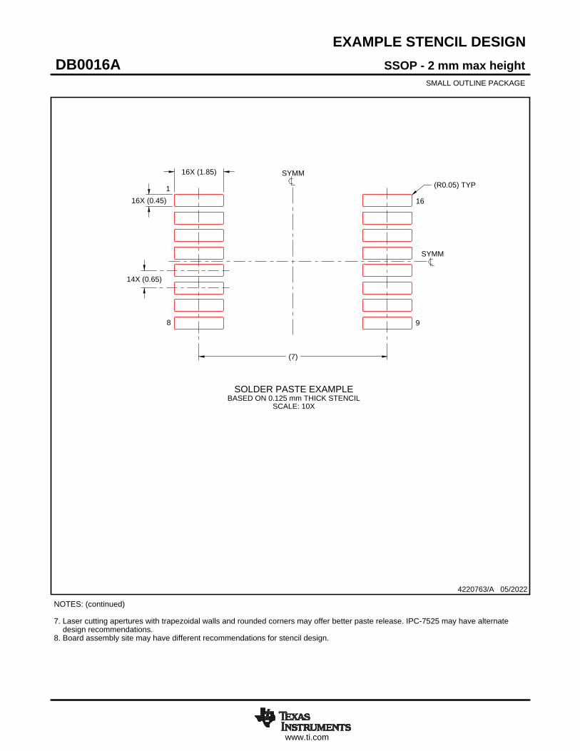
EXAMPLE STENCIL DESIGN
(7)(R0.05) TYP
16X (1.85)
16X (0.6)
14X (1.27)
4220735/A 12/2021
SOP - 2.00 mm max heightNS0016ASOP
NOTES: (continued) 7. Laser cutting apertures with trapezoidal walls and rounded corners may offer better paste release. IPC-7525 may have alternate design recommendations. 8. Board assembly site may have different recommendations for stencil design.
SOLDER PASTE EXAMPLEBASED ON 0.125 mm THICK STENCIL
SCALE:7X
SYMM
SYMM
1
8 9
16
www.ti.com
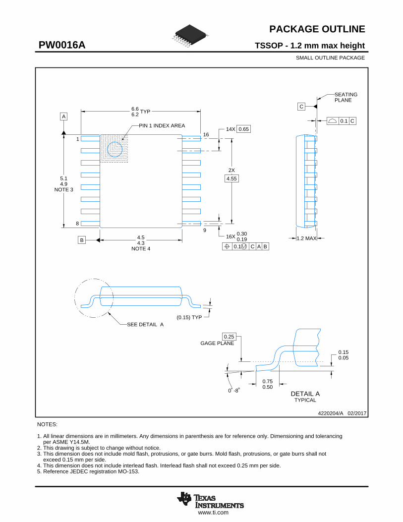
PACKAGE OUTLINE
C
14X 0.65
2X4.55
16X 0.300.19
TYP6.66.2
1.2 MAX
0.150.05
0.25GAGE PLANE
-80
BNOTE 4
4.54.3
A
NOTE 3
5.14.9
0.750.50
(0.15) TYP
TSSOP - 1.2 mm max heightPW0016ASMALL OUTLINE PACKAGE
4220204/A 02/2017
1
89
16
0.1 C A B
PIN 1 INDEX AREA
SEE DETAIL A
0.1 C
NOTES: 1. All linear dimensions are in millimeters. Any dimensions in parenthesis are for reference only. Dimensioning and tolerancing per ASME Y14.5M. 2. This drawing is subject to change without notice. 3. This dimension does not include mold flash, protrusions, or gate burrs. Mold flash, protrusions, or gate burrs shall not exceed 0.15 mm per side. 4. This dimension does not include interlead flash. Interlead flash shall not exceed 0.25 mm per side.5. Reference JEDEC registration MO-153.
SEATINGPLANE
A 20DETAIL ATYPICAL
SCALE 2.500
www.ti.com
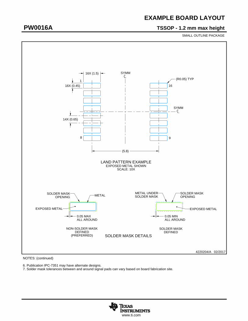
EXAMPLE BOARD LAYOUT
0.05 MAXALL AROUND
0.05 MINALL AROUND
16X (1.5)
16X (0.45)
14X (0.65)
(5.8)
(R0.05) TYP
TSSOP - 1.2 mm max heightPW0016ASMALL OUTLINE PACKAGE
4220204/A 02/2017
NOTES: (continued) 6. Publication IPC-7351 may have alternate designs. 7. Solder mask tolerances between and around signal pads can vary based on board fabrication site.
LAND PATTERN EXAMPLEEXPOSED METAL SHOWN
SCALE: 10X
SYMM
SYMM
1
8 9
16
15.000
METALSOLDER MASKOPENING
METAL UNDERSOLDER MASK
SOLDER MASKOPENING
EXPOSED METALEXPOSED METAL
SOLDER MASK DETAILS
NON-SOLDER MASKDEFINED
(PREFERRED)
SOLDER MASKDEFINED
www.ti.com
EXAMPLE STENCIL DESIGN
16X (1.5)
16X (0.45)
14X (0.65)
(5.8)
(R0.05) TYP
TSSOP - 1.2 mm max heightPW0016ASMALL OUTLINE PACKAGE
4220204/A 02/2017
NOTES: (continued) 8. Laser cutting apertures with trapezoidal walls and rounded corners may offer better paste release. IPC-7525 may have alternate design recommendations. 9. Board assembly site may have different recommendations for stencil design.
SOLDER PASTE EXAMPLEBASED ON 0.125 mm THICK STENCIL
SCALE: 10X
SYMM
SYMM
1
8 9
16
www.ti.com
PACKAGE OUTLINE
C
14X 0.65
2X4.55
16X 0.380.22
8.27.4 TYP
SEATINGPLANE
0.05 MIN
0.25GAGE PLANE
0 -8
2 MAX
0.250.09
B 5.65.0
NOTE 4
A
6.55.9
NOTE 3
0.950.55
SSOP - 2 mm max heightDB0016ASMALL OUTLINE PACKAGE
4220763/A 05/2022
1
89
16
0.1 C A B
PIN 1 INDEX AREA
SEE DETAIL A
0.1 C
NOTES: 1. All linear dimensions are in millimeters. Any dimensions in parenthesis are for reference only. Dimensioning and tolerancing per ASME Y14.5M. 2. This drawing is subject to change without notice. 3. This dimension does not include mold flash, protrusions, or gate burrs. Mold flash, protrusions, or gate burrs shall not exceed 0.15 mm per side. 4. Reference JEDEC registration MO-150.
A 15DETAIL ATYPICAL
SCALE 1.500
www.ti.com
EXAMPLE BOARD LAYOUT
0.05 MAXALL AROUND
0.05 MINALL AROUND
16X (1.85)
16X (0.45)
14X (0.65)
(7)
(R0.05) TYP
SSOP - 2 mm max heightDB0016ASMALL OUTLINE PACKAGE
4220763/A 05/2022
NOTES: (continued) 5. Publication IPC-7351 may have alternate designs. 6. Solder mask tolerances between and around signal pads can vary based on board fabrication site.
LAND PATTERN EXAMPLEEXPOSED METAL SHOWN
SCALE: 10X
SYMM
SYMM
1
8 9
16
15.000
METALSOLDER MASKOPENING
METAL UNDERSOLDER MASK
SOLDER MASKOPENING
EXPOSED METALEXPOSED METAL
SOLDER MASK DETAILS
NON-SOLDER MASKDEFINED
(PREFERRED)
SOLDER MASKDEFINED
www.ti.com
EXAMPLE STENCIL DESIGN
16X (1.85)
16X (0.45)
14X (0.65)
(7)
(R0.05) TYP
SSOP - 2 mm max heightDB0016ASMALL OUTLINE PACKAGE
4220763/A 05/2022
NOTES: (continued) 7. Laser cutting apertures with trapezoidal walls and rounded corners may offer better paste release. IPC-7525 may have alternate design recommendations. 8. Board assembly site may have different recommendations for stencil design.
SOLDER PASTE EXAMPLEBASED ON 0.125 mm THICK STENCIL
SCALE: 10X
SYMM
SYMM
1
8 9
16
IMPORTANT NOTICE AND DISCLAIMERTI PROVIDES TECHNICAL AND RELIABILITY DATA (INCLUDING DATA SHEETS), DESIGN RESOURCES (INCLUDING REFERENCE DESIGNS), APPLICATION OR OTHER DESIGN ADVICE, WEB TOOLS, SAFETY INFORMATION, AND OTHER RESOURCES “AS IS” AND WITH ALL FAULTS, AND DISCLAIMS ALL WARRANTIES, EXPRESS AND IMPLIED, INCLUDING WITHOUT LIMITATION ANY IMPLIED WARRANTIES OF MERCHANTABILITY, FITNESS FOR A PARTICULAR PURPOSE OR NON-INFRINGEMENT OF THIRD PARTY INTELLECTUAL PROPERTY RIGHTS.These resources are intended for skilled developers designing with TI products. You are solely responsible for (1) selecting the appropriate TI products for your application, (2) designing, validating and testing your application, and (3) ensuring your application meets applicable standards, and any other safety, security, regulatory or other requirements.These resources are subject to change without notice. TI grants you permission to use these resources only for development of an application that uses the TI products described in the resource. Other reproduction and display of these resources is prohibited. No license is granted to any other TI intellectual property right or to any third party intellectual property right. TI disclaims responsibility for, and you will fully indemnify TI and its representatives against, any claims, damages, costs, losses, and liabilities arising out of your use of these resources.TI’s products are provided subject to TI’s Terms of Sale or other applicable terms available either on ti.com or provided in conjunction with such TI products. TI’s provision of these resources does not expand or otherwise alter TI’s applicable warranties or warranty disclaimers for TI products.TI objects to and rejects any additional or different terms you may have proposed. IMPORTANT NOTICE
Mailing Address: Texas Instruments, Post Office Box 655303, Dallas, Texas 75265Copyright © 2022, Texas Instruments Incorporated
Related Documents