Linear Feedback Shift Registers (LFSR) © John Knight Dig Cir p. 217 Revised; November 18, 2003 Linear Feedback Shift Registers (LFSR) A type of circuit made from XOR and D ff which give repeatable “random” numbers. 1 0 0 0 0 1 0 0 0 0 1 0 0 0 0 1 1 1 0 0 0 1 1 0 0 0 1 1 1 1 0 1 1 0 1 0 CLK 1D X 4 X 3 X 2 X 1 C1 0 1 0 1 1D C1 1D C1 1D C1 1 1 1 0 0 1 1 1 1 1 1 1 1 0 1 1 1 0 0 1 8 4 2 1 10 6 3 13 12 5 14 7 15 11 9 0 0 0 0 0 1 0 0 0 0 1 0 0 0 0 1 0 1 0 0 1 1 1 0 0 0 1 1 0 1 0 1 1 0 1 0 1 1 0 1 0 CLK 1D X 0 X 1 X 2 X 3 C1 1 1 0 1 1D C1 1D C1 1D C1 1 1 1 0 1 1 1 1 0 1 1 1 0 0 1 1 0 0 0 1 8 4 2 9 12 6 11 5 10 13 14 15 7 3 1 0 0 0 0 0 clock cycles Internal circuit, XORs inside shift reg. External circuit, XORs outside shift reg. 1+X+X 4 1 X X 4 1 X X 4 X 4 + X +1 Slide 109 Carleton University © John Knight Vitesse Digital Circuits p. 218 Revised; November 18, 2003 Linear Feedback Shift Registers (LFSR) Linear Feedback Shift Registers Linear Feedback Shift Registers Properties Names Linear-Feedback Shift-Register ( LFSR), Autonomous LFSR, Pseudo-Random-Number Generators, Polynomial Sequence Generators, Pseudo-Random-Pattern generators, etc. Math The connections to the feedback loop are given placeholder names which are powers of X. One end is always X 0 =1, the other is always X n . The others are X k if there is an XOR connection at k. The powers of X define a polynomial. If the polynomial is what we call primitive, the circuit will sequence through 2 N -1 numbers for N flip-flops. Else it will have several shorter sequences and will not be much use. Circuits There are four circuits with the same polynomial and close to the same properties: An internal circuit. An external circuit. An internal circuit with the connections and labelling reversed An external circuit with the connections and lab The polynomials are the same. If one is primitive they both are. However the sequencing of the numbers will be different. Primitive Polynomials They are listed in many books. 1 1. V.N. Yarmolik, and I.V Kachan, Self Testing VLSI Design, Elsevier 1993. It goes up to 300 flip-flops. 1 X 3 X 1 1 X 3 X 1 Comment on Slide 109

Welcome message from author
This document is posted to help you gain knowledge. Please leave a comment to let me know what you think about it! Share it to your friends and learn new things together.
Transcript

Linear Feedback Shift Registers (LFSR)
© John Knight
Dig Cir p. 217 Revised; November 18, 2003
Linear Feedback Shift Registers (LFSR)A type of circuit made from XOR and D ff which give repeatable “random” numbers.
1 0 0 00 1 0 00 0 1 00 0 0 11 1 0 00 1 1 00 0 1 11 1 0 11 0 1 0
CLK1D
X4X3X2X1
C1
0 1 0 1
1D
C1
1D
C1
1D
C1
1 1 1 00 1 1 11 1 1 11 0 1 11 0 0 1
84
21
106
313
125
147
1511
90 0 0 00
1 0 0 00 1 0 00 0 1 01 0 0 11 1 0 00 1 1 01 0 1 10 1 0 11 0 1 0
CLK1D
X0X1X2X3
C1
1 1 0 1
1D
C1
1D
C1
1D
C1
1 1 1 01 1 1 10 1 1 10 0 1 10 0 0 1
84
29
126
115
1013
1415
73
10 0 0 00
clo
ck
cy
cle
s
Internal circuit, XORs inside shift reg. External circuit, XORs outside shift reg.
1 + X + X4
1 X X4 1XX4
X4+ X +1
Slide 109
Carleton University © John Knight Vitesse
Digital Circuits p. 218 Revised; November 18, 2003
Linear Feedback Shift Registers (LFSR) Linear Feedback Shift Registers
Linear Feedback Shift RegistersProperties
Names
Linear-Feedback Shift-Register ( LFSR), Autonomous LFSR, Pseudo-Random-Number Generators,Polynomial Sequence Generators, Pseudo-Random-Pattern generators, etc.
Math
The connections to the feedback loop are given placeholder names which are powers of X.One end is always X0=1, the other is always Xn. The others are Xk if there is an XOR connection at k.
The powers of X define a polynomial.If the polynomial is what we call primitive, the circuit will sequence through 2N-1 numbers for N flip-flops.Else it will have several shorter sequences and will not be much use.
Circuits
There are four circuits with the same polynomial and close to the same properties:An internal circuit.An external circuit.An internal circuit with the connections and labelling reversedAn external circuit with the connections and lab
The polynomials are the same. If one is primitive they both are.However the sequencing of the numbers will be different.
Primitive Polynomials
They are listed in many books.1
1. V.N. Yarmolik, and I.V Kachan, Self Testing VLSI Design, Elsevier 1993. It goes up to 300 flip-flops.
1 X3X1
1X3 X1
Comment on Slide 109

Linear Feedback Shift Registers
© John Knight
Dig Cir p. 219 Revised; November 18, 2003
Linear Feedback Shift RegistersProperties of LFSR
Names• Linear-Feedback Shift-Register ( LFSR), Pseudo-Random-Number Generators,
Polynomial Sequence Generators etc., etc.
• Individual circuits have polynomial names related to their connections; i.e. 1 + X + X4
• Can deduce the properties of the circuit from its polynomial. (and a math degree)
• Use certain polynomials called primitive.
Circuit
• Uses only a few (1 to 3) XOR gates, and D flip-flops.
• Internal circuit is very fast. Max delay = (1 XOR delay) + (1 D ff delay).
• Primitive polynomials have 2N-1 sequential states.
• The all zero state is always isolated.If you reset a LFSR at the start, it locks up in the all zero state.
Randomness (primitive polynomials)• It obeys 15 of 25 standard statistical tests
• Consecutive numbers have a shift register relation (particularly external).Columns are identical but displaced (see background shading).
• No number is repeated until the complete sequence is done.
• Mean = -1/(2N -1)� slight dc biasThere is one more 1 than there are 0s in any column.
Slide 110
Carleton University © John Knight Vitesse
Digital Circuits p. 220 Revised; November 18, 2003
Linear Feedback Shift Registers Linear-Feedback Shift-Registers (cont.)
Comment on Slide 110
Linear-Feedback Shift-Registers (cont.)Properties
Size
A LFSR takes less area than any other common counter except a ripple counter.
The ripple counter is not synchronous and much harder to interface reliably.
Speed
A LFSR is faster than any other common counters except the Mobius counter.
Counting
It does not count in binary. It counts modulo 2N-1, a binary counter counts modulo 2N.
Applications
Where one needs to count a fixed time, but do not need to need arithmetic compatible intermediate values.Time out counts; shut off the screen if no one touched the keyboard for 2N-1 seconds.
Send an input to the control computer every 100ms, reboot if no response.
Cycling through addresses for refreshing DRAM. T he order ofrefresh does not matter. Not going through address 0000 might matter.
1.• PROBLEM
In any LFSR, insert the following circuit between two adjacent flip-flops which were not previously connected through an XOR. Theprevious state graph will have looked like that of the "Linear-FeedbackShift-Registers (cont.)," p. 220.(a) What will the new state graph look like?(b) What will happen if you start by resetting all the flip-flops? CLK
All flip-flops except Qx
Qx
RRRR

Linear Feedback Shift Registers
© John Knight
Dig Cir p. 221 Revised; November 18, 2003
Linear-Feedback Shift-Registers (cont.)
Example of a Nonprimitive Polynomial
1 0 0 00 1 0 00 0 1 00 0 0 11 1 0 11 0 1 10 1 1 00 0 1 11 1 0 0
CLK1D
X4X3X2X1
C1
0 1 0 1
1D
C1
1D
C1
1D
C1
1 0 1 01 1 1 10 1 1 11 1 1 01 0 0 1
84
21
1311
63
125
1015
714
90 0 0 00
CLK1D
X0X1X2X3
C1
1D
C1
1D
C1
1D
C1
clo
ck
cy
cle
sInternal circuit, XORs inside shift reg. External circuit, XORs outside shift reg.
1 + X + X3 + X4
1 X X4 1XX4
X4 + X3+ X +1
1 0 0 01 1 0 01 1 1 00 1 1 10 0 1 10 0 0 11 1 0 10 1 1 01 0 1 10 0 1 11 0 0 10 1 0 00 1 0 11 0 1 01 1 1 1
812
147
31
136
112
94
510
150 0 0 00
Slide 111
Carleton University © John Knight Vitesse
Digital Circuits p. 222 Revised; November 18, 2003
Linear Feedback Shift Registers Linear-Feedback Shift-Registers (cont.)
Comment on Slide 111
Minimal Hardware, Primitive Polynomials• 1+ x + x2 1+ x + x3 1+ x + x4 1+ x2 + x5 1+ x + x6 1+ x + x7
1+ x + x5+ x6 + x8 1+ x4 + x9 1+ x3+ x10 1+ x2+ x11 1+ x3 +x4+x7+x12
1+ x + x3+ x4 + x13 1+ x+ x15 1+x2+x3+x5+x16 1+ x3+ x17 1+ x7+ x18 1+ x3+ x20
1+ x2+ x21 1+ x+ x22 1+x5+x23 1+x+x3+x4+x24 1+x3+x25 1+x+x7+x8+x26
• For N flip-flops, one seems to only need 3 or fewer XOR gates.
Starting
• All LFSR lockup in the all zero state. A very reliable circuit would check if the flip-flops are all zeroand inject a one. Less reliable circuits will initialize some of the flip-flops to one.
Randomness• The numbers as integers look random. The numbers as bit patterns show the shifting strongly.
• Some applications, like testing with random numbers, scramble the leads going to the various flip-flops. This gives a better test for multipliers or barrel shifters.
Bias• Some communication circuits do not like inputs that have a dc bias.
To make a random generator that has no bias, and includes zero,Take the output of the most significant bit of the generator though aninverter. This will change 100...0, the most negative 2’s complementnumber, into 000...0, and balance the plus and minus numbers
2.• PROBLEM
Modify the Verilog code for the shift register to make a LFSR for 7 flip-flops (1+ x + x7).
011010001
111110101100
011010001000111110101100
111110101000011010001
3210
-1-2-3-4
dec2’s
LFSR(no zero)
compl
LFSRwithinverter

Linear Feedback Shift Registers
© John Knight
Dig Cir p. 223 Revised; November 18, 2003
Verilog LFSR• One can specify a subset of bits like Reg[4:2].
• One must not reset a LFSR to 0.
Nonblocking AssignmentThe <= assignment in procedures is called nonblocking.
The variables on the right of <= are captured in parallel on the @ trigger.
The variables on the left are always calculated from these initial values.
• It is a master-slave like operation.
• If one uses nonblocking anywhere in a procedure one must use it everywhere.
module LFSR2(Reg, clk, reset);parameter n=4 // Change more than n to change LFSR length.output[n:1]Reg;reg [n:1]Reg; //All procedure outputs must be registeredinput clk reset;
always @(posedge clkor posedge reset)
if(reset) Reg <=1;elseReg <= {Reg[n-1:2], Reg[n]^Reg[1], Reg[n]};
endmodule //LFSR2
X2
X4+ X +11XX4 X3
Slide 112
Carleton University © John Knight Vitesse
Digital Circuits p. 224 Revised; November 18, 2003
Linear Feedback Shift Registers Verilog LFSR
Comment on Slide 112
Verilog LFSRReset To Zero
One must never clear a LFSR. If the flip-flops have a set, use it. If notplace inverters before and after the flip-flop to fake a set.
Parameters
Parameters are very handy. I would recommend using them frequently.Here changing n will not be enough to change the LFSR. One must check that the XOR is in the right place for the largersize. However it saves having to change output, reg and other statements.
always @(posedge clk or posedge reset)
The @ is the edge triggered signal. Most counters, registers, flip-flops should start with this way.
Blocking and Nonblocking
Normal blocking assignment in procedures is via the “=.” Such variables behave like a normal program. Thus:R[1]= R[n];
will replace R[1]. Then:R[2] = R[n]^R[1];
will use the revised R[1] in the calculation. This is not what is wanted!
Nonblocking assignment uses the “<=” symbol. Nonblocking assignment is more like a register of D flip-flops. Theinputs are transfered across the “<=” at once in the same way that all flip-flops are clocked at once.
Use Nonblocking <= for Flip-flops, Counters and Shift Registers
Your reflex action should be to use “<=” for all procedures containing flip-flops.
RESET R R R R

Linear Feedback Shift Registers
© John Knight
Dig Cir p. 225 Revised; November 18, 2003
Application of the LFBSR:
The Circular Queue (FIFO)Locating Queue Empty and Queue Full require comparing present and previous pointersA shift-register can remember its previous state using 1 extra ff.LFSR is smaller and faster than a binary counter.The strange counting order of the LFSR does not matter.
11101101
1111
1100
101010011000
1011
01110110010101000011001000010000
11101101
1111
1100
101010011000
1011
01110110010101000011001000010000
+1
4
4+1
4
4
Prev_RPtr
RPtr
Prev_WPtr
WPtr
Empty= ((RPTR==Prev_WPtr)&Read);
Full = ((WPTR==Prev_RPtr)&Write); 1DC1
EMPTY
1DC1
FULL
01111111
0011
1110
101001011011
1101
01101100100100100100100000010000
RPtr
Prev_WPtr
WPtr4 4
4-to-16Decode
4-to-16Decode
Queue
Prev_RPtr
4
01111111
0011
1110
101001011011
1101
01101100100100100100100000010000
Using N-bit Binary Counters Using LFSRUse 4N ffIncrementer hardware x2
Use 2N+2 ff2 XOR gates
Counter carry-chain delay (next p.) 1 XOR gate delay
Empty= ((RPTR==Prev_WPtr)&Read);
Full = ((WPTR==Prev_RPtr)&Write); 1DC1
EMPTY
1DC1
FULL
2N+4 for 2N queue6 for a 2 a N queue3 for a 2N queue
Slide 113
Carleton University © John Knight Vitesse
Digital Circuits p. 226 Revised; November 18, 2003
Linear Feedback Shift Registers Verilog LFSR
Comment on Slide 113
Applications of LFSR
Circular Queue or First-In-First-Out Register
Queue full and queueempty both have:-
Wptr = RPtrTo tell full from emptycompare the pointers. If
WPtr =RPtr -1and one is writing, thatwrite will fill the queueand should set a full flag.
Similarly ifRPtr =WPtr -1 i.e. RPtr = Previous WPtr
and one is reading, then that read will empty thequeue. One should set an empty flag and allow nomore reads until after a write.
3.• PROBLEM
Implement the queue with 2*2N bit shift registers.
121
34567
92
8
READPOINTER
WRITEPOINTER
QUEUEEMPTY
R Ptr=W Ptr
Write 1WPtr=R Ptr + 1 WPtr=RPtr + 1
Write 2QUEUEFULL
WPtr=RPtr
WPtrWPtr
WPtrRPtr RPtr
RPtr2
Read 1
WPtrRPtr
WPtr=RPtr + 2
2345
WPtr=RPtr + 5
Write 3,4,5,6
WPtr
RPtr
6
Two pointers move up the register bank in response to reads and writes.
RPtr WPtr
EMPTYRPtr=WPtr
QUEUE
34567
92
8
QUEUEFULL
RPtr=WPtr
WPtrRPtr2345
WPtr=RPtr - 1
ALMOST
WPtrRPtr
678
2
ALMOST
RPtr=WPtr - 1
WPtrRPtr
EMPTY FULL
FULLEMPTY
READ
WRITE
RPtr
Prev RPtr
WPtr
Prev WPtr
1DC1
1DC1
FULLNo more Writes until Read
EMPTYNo more Reads until Write
EQUALS
Write
EQUALS
Read

Binary Counters
© John Knight
Dig Cir p. 227 Revised; November 18, 2003
Binary Counters
Binary Up-Counter
Simplest Circuit Uses T Flip-Flops(Simplest for People)
The T table shows where bits toggle going betweenthe present state and the next state.
The circles show how the toggle signals aredefined by ANDs:
T1 = Q0T2 = Q1Q0T3 = Q2Q1Q0TC = Q3Q2Q1Q0
Propagation DelayNotice the ripple carry. All binary counter havethis speed limiting carry.
c
Present State Next State What to ToggleQ3 Q2 Q1 Q0 Q3 Q2 Q1 Q0 T3 T2 T1 T0
0 0 0 0 0 0 0 1 T
0 0 0 1 0 0 1 0 T T
0 0 1 0 0 0 1 1 T
0 0 1 1 0 1 0 0 T T T
0 1 0 0 0 1 0 1 T
0 1 0 1 0 1 1 0 T T
0 1 1 0 0 1 1 1 T
0 1 1 1 1 0 0 0 T T T T
1 0 0 0 1 0 0 1 T
1 0 0 1 1 0 1 0 T T
1 0 1 0 1 0 1 1 T
1 0 1 1 1 1 0 0 T T T
1 1 0 0 1 1 0 1 T
1 1 0 1 1 1 1 1 T T
1 1 0 0 1 1 1 1 T
1 1 1 1 0 0 0 0 T T T T
1T
C1
CLK
1T
C1
1T
C1
1T
C1
Q0Q1Q2Q3
A 4-bit binary counter
T3 T2 T1
C
T0
Slide 114
Carleton University © John Knight Vitesse
Digital Circuits p. 228 Revised; November 18, 2003
Binary Counters Binary Up-Counter
Comment on Slide 114
Binary Up-CounterDesign of the Counter
The Karnaugh maps for the toggle inputs are given below. Many people are more used to them, and they are much lesserror prone than picking bits off the state tables.
Simplicity
This counter looks much simpler than most textbook counters. However if one implements it with D flip-flops,converting to enabled toggle flip-flop requires an XOR for each flip-flop. Thus it is simple for the designer, but it is onlyapparent simplicity.
Speed
The binary counter is one form of binary adder. The slow carry chain is present. For long counts the carry chain andcounter will be quite slow
To get around this one could use a LFSR. It will count quickly, but one cannot do arithmetic on its result. One cannoteasily tell if the signal is greater than some reference. One can only tell equality easily.
Map for T3 Map for T2 Map for T1 Map for T0
00 01 11 10 00 01 11 10 00 01 11 10 00 01 11 1000 0 0 0 0 00 0 0 1 0 00 0 1 1 0 00 1 1 1 101 0 0 1 0 01 0 0 1 0 01 0 1 1 0 01 1 1 1 111 0 0 1 0 11 0 0 1 0 11 0 1 1 0 11 1 1 1 110 0 0 0 0 10 0 0 1 0 10 0 1 1 0 10 1 1 1 1
Q3Q2
Q1Q0Q3Q2
Q1Q0Q3Q2
Q1Q0Q3Q2
Q1Q0
Binary Counters
© John Knight
Dig Cir p. 229 Revised; November 18, 2003
Binary Down-Counter
T Flip-Flops Circuit(Simplest for People)
The T table shows where the bits toggle in goingto the next state.
The circles show how the toggle signals aredefined by zeros:
T(L) means a “0” togles the flip-flop.
c
Present State Next State What to ToggleQ3 Q2 Q1 Q0 Q3 Q2 Q1 Q0 T3 T2 T1 T0
0 0 0 0 1 1 1 1
1 1 1 1 1 1 1 0 T
1 1 1 0 1 1 0 1 T T
1 1 0 1 1 1 0 0 T
1 1 0 0 1 0 1 1 T T T
1 0 1 1 1 0 1 0 T
1 0 1 0 1 0 0 1 T T
1 0 0 1 1 0 0 0 T
1 0 0 0 0 0 0 0 T T T T
0 1 1 1 0 1 1 0 T
0 1 1 0 0 1 0 1 T T
0 1 0 1 0 1 0 0 T
0 1 0 0 0 0 1 1 T T T
0 0 1 1 0 0 1 0 T
0 0 1 0 0 0 0 1 T T
0 0 0 1 0 0 0 0 T
1T
C1
CLK
1T
C1
1T
C1
1T
C1
Q0Q1Q2Q3
A 4-bit binary down counter
T3(L) T2(L) T1(L)
C
T0
T1(L) = Q0 =Q0T2(L) = Q1Q0 =Q1+Q0T3(L) = Q2Q1Q0 =Q2+Q1+Q0TC(L) = Q3Q2Q1Q0 =Q3+Q2+Q1+Q0
Slide 115
Carleton University © John Knight Vitesse
Digital Circuits p. 230 Revised; November 18, 2003
Binary Counters Binary Down-Counter
Comment on Slide 115
Binary Down-CounterDesign of the Counter
This counter is very much like the up-counter. The difference is the toggle signals are generated by checking for groupsof zero flip-flop outputs, such as Q2Q1Q0. Using DeMorgan’s theorem changes these terms to a chain of OR gatesinstead of AND gates.
Up-Down Counters
A controllable up-down counter is made by switching between the up and down circuits.
T3= (up_dwn) ? Cup : (~Cdwn);
Cup = Q_1&Cup_1
Cdwn = Q_1&Cdwn_1
1T
C1
CLK
Q0T0T3 T2
1T
C1
Q1T1
1
G11
MUX
1
G11
MUX1
G11
MUX
T31T
C1
Q21
G11
MUX
1T
C1
Q3
UP_DWN
TC
UP_DWN
Cdwn
Cup
Cdwn_1
Cup_1

Binary Counters
© John Knight
Dig Cir p. 231 Revised; November 18, 2003
Preloadable CountersConstructed from the Basic Counter Module
TKQK
1T
C1
1T
C1
1D 1T
C1
1D2
G22
MUX
3,1D
M31T
C1
1D2
G22
MUX
3,1D
M3
QK
CLK
PR
COUTCIN
QK TK
(A) Basic module (bit-slice)for a binary counterusing a T flip-flop
(B) The T flip-flop made from aD flip-flop
(C) Specialized flip-flop forpreloadable counter module
(D) Basic module for a preloadablecounter
TKQK 3,1T
C1
3,1D
M3 PRCLK
CINCOUTXK
XK
(C) The T flip-flop madepreloadable
TK
XK
Mode 3 selects the input.
Slide 116
Carleton University © John Knight Vitesse
Digital Circuits p. 232 Revised; November 18, 2003
Binary Counters Preloadable Counters
Comment on Slide 116
Preloadable CountersHiearchy
The preloadable counter is a hierarchy of modules starting with a D flip-flop.
a. D flip-flop
b. Preloadable D flip-flop
c. Preloadable T flip-flop
d. The Counter Module With AND Gate.
e. The Preloadable Up-Counter
IEEE Symbols
The PR input changes the mode. The number 3 was picked for the mode. In mode 3, the circuit (C) and (D) do a preloadon the clock edge. The “3,1D” says that in mode 3 and (comma and) on the “1” signal edge this is a D input.
The control number in the MUX was changed to 2 because, in this symbol, 1 was already used by the clock.
Any numbers can show a connection between a control an what it controls. However the number must be the same atboth sides. Thus 2 controls 2.

Binary Counters
© John Knight
Dig Cir p. 233 Revised; November 18, 2003
Preloadable Counters (cont.)Counters That Count to Something Besides 2N
(B) Specialized flip-flop forpreloadable counter module
TKQK3,1T
C1
3,1D
M3
CIN
COUT
XK
C1/3+
3,1D
3,1D
3,1D
3,1D
3,1D
M3
CLK
PR
Q0
Q1
Q2Q3
Q4
(A) Preloadable Counter
Mode 3: Binary Up-Counter “3+”
CTR5
Mode 3: Synchronous (Clocked) load
X0
X1
X2
X3
X4
Need both mode 3 and clockedge “3,1D” to load.
C1/3+
3,1D
3,1D
3,1D
3,1D
3,1D
M3CLK
PR
Q0
Q1
Q2Q3
Q4
CTR5Common clockand mode control
(C) Mod 22 counter.Counts 0 to 21 (5'b10101;) and repeats.
5 counter modules
PRCLK
C1/3-
3,1D
3,1D
3,1D
3,1D
3,1D
M3CLK
PR
Q0
Q1
Q2Q3
Q4
CTR5
(D) Mod 22 down counter.Counts 21 to 0 and repeats.
Slide 117
Carleton University © John Knight Vitesse
Digital Circuits p. 234 Revised; November 18, 2003
Binary Counters Preloadable Counters (cont.)
Preloadable Counters (cont.)
IEEE Counter Symbol
The symbol is divided into 5 special modules and a common T shaped control block.
• The control block contains the letters CTR5 to show the circuit is basically a 5 bit counter.
• The common mode control “M3” for preloading.
• The common clock input “C1/3+.” The “+” says the counting is binary and upwards unless one is inmode 3. The C1 says it functions as a clock independent of mode.
• “+” after the clock input is an up counter. “-” after the clock input is a down counter.
Counting to M≠2N
Decode Terminal Count
Decode, with the equivalent of a many input AND gate, the final count. Use that to activate the preload and load zero.This allows the counting to go upwards.
Preload the Maximum Count and Count Down
At the start of counting, loading the maximum count and count down.Alternately load the two’s complement of the maximum count, and count up.
This is a better method if the desired count keeps changing. One does not need a different AND gate for each count.
Comment on Slide 117n
Binary Counters
© John Knight
Dig Cir p. 235 Revised; November 18, 2003
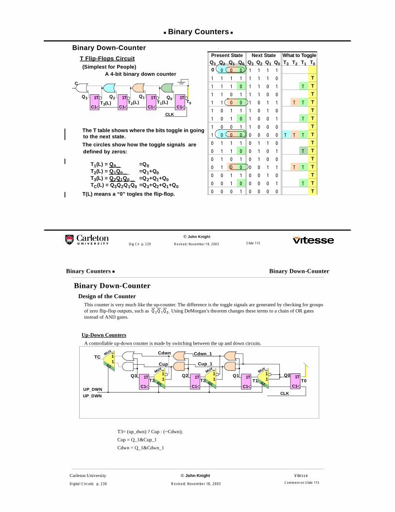
A Verilog Preloadable Up/Down Countermodule UpDwn(Q, updwn, X, pr, clk, reset);
parameter n=4;input [n-1:0] X; // The number to preload into counterinput pr, updwn, // preset control, up(H)/down(L)
clk, rst; // clock, asynchronous reset
output[n-1:0] Q;wire [n-1:1] Cup, Cdwn; // The carries for up and down counting.
pr_T_ff ff0(Q[0],X[0], 1, pr, clk, rst);cntr cir1(Q[1], Cup[1],Cdwn[1], Q[0], Q[0], updwn, X[1], pr, clk, rst);
cntr cir2(Q[2], Cup[2], Cdwn[2], Cup[1], Cdwn[1], updwn, X[2], pr, clk, rst);
cntr cir3(Q[3], Cup[3],Cdwn[3], Cup[2], Cdwn[2], updwn, X[3], pr, clk, rst);
endmodule UpDwn
updwnreset
Q[2]
11
1T3,1D
M3
R
X[2]Q[3]
11
1T3,1D
M3
R
X[3]
Cup[2]
Cdwn[2]
rst
Q[1]
11
1T3,1D
M3
R
X[1]
Cup[1]
Cdwn[1]
1T
C1
3,1D
M3
R
clk
X[0]Q[0]
clkclkclk
ff0cir1cir2cir3
Slide 118
Carleton University © John Knight Vitesse
Digital Circuits p. 236 Revised; November 18, 2003
Binary Counters Named Module Connections (Named
A Verilog Preloadable Up/Down Counter (cont)
A Counter ModuleThe four components on the diagram are easily spotted in the code.
• The flip-flop is the module call.pr_T_ff ff1(Qi, Xi,Ti, pr, clk, reset);
• The & gateCup = Cup_1 & Qi,
• The OR “|” gate.Cdwn= Cdwn_1 | Qi,
• The MUXTi=(updwn) ? Cup_1 : ~Cdwn_1;
This Module is Structual
The connections are described. Not the operation.
Named Module Connections (Named Ports)The connections between a module definition and its instantiation have been made by position.The shaded box shows how to make the connections by using the module port name.<port name used in the original definition>.(<wire/reg name connecting this particular instantiation>)
.T(Ti)
For small modules position is simpler.For large modules name is better. Errors in position are easy to make with 20 or more variables.
Note this has nothing to do with call by name/call by value described in programming courses.
Comment on Slide 118

Binary Counters
© John Knight
Dig Cir p. 237 Revised; November 18, 2003
A Verilog Preloadable Up/Down Countermodule cntr(Qi,Cup, Cdwn, Cup_1, Cdwn_1, updwn, Xi, pr, clk, rst);
input Cup_1, Cdwn_1, updwn, Xi, pr, clk, rst;output Qi, Cup, Cdwn;wire Ti;
assignCup = Cup_1 & Qi,Cdwn = Cdwn_1 | Qi,Ti = (updwn) ? Cup_1 : ~Cdwn_1;pr_T_ff ffByPos(Qi, X, Ti, pr, clk, rst);
// Alternate connection of module ports (arguments) by name.// The position of the argument is no longer important.// pr_T_ff ff ByName( .X(Xi), .T(Ti), .Q(Qi), .RST(rst), .CLK(clk), .PR(pr);
endmodule // cntr
Ti 1
G11
MUX
Qi
Cdwn
Cup Cup_1
Cdwn_1
updwn
rst
Xi bit to preload
clk
T1T
C1
3,1D
M3R
CLK
Q
pr_T_ff
PR
RST
T1T
C1
3,1D
M3R
CLK
Q
PR
RST
X X
pr
wireport name
port names
Slide 119
Carleton University © John Knight Vitesse
Digital Circuits p. 238 Revised; November 18, 2003
Binary Counters A Verilog Preloadable Up/Down Counter
A Verilog Preloadable Up/Down Counter (cont)
The Flip-Flop ModuleThis module follows the classic flip-flop standard:
• All outputs, or variables on the right-hand-side of a procedure must be of type reg.reg Qi;
• The flip-flop is edge triggered, @, and has an asynchronous reset.always @(posedge clk or posedge reset)The asynchronous reset allows the system to be placed in a known state during start-up. Synchronousreset requires the co-operation of the clock. A system with clock and clock/2 for example, has to becarefully planned to reset properly using synchronous reset.
• The nonblocking assignment “<=” is used.Qi <= (pr) ? Xi : Qi^Ti;Thus flip-flop outputs, fed back into flip-flop inputs, always use the previous values for inputs.For example Q[2]<=Q[1]; Q[1]<=Q[2]; always exchanges Q[1] and Q[2].
The Interaction of XOR and Toggle
The logic for Qi^Ti requires a little thought:
Qi is the fed back flip-flop output.Ti is the toggle enable.
• When Ti=1, the flip-flop toggles i.e. ~Qi is fed back.
• When Ti=0, the flip-flop holds is old value, i.e. Qi is fed-back.
This reduces to Qi <= Qi^Ti.
Comment on Slide 119
Binary Counters
© John Knight
Dig Cir p. 239 Revised; November 18, 2003
A Verilog Preloadable Up/Down Counter (cont)
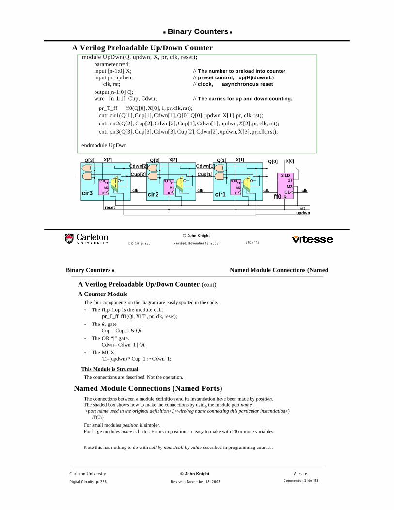
module pr_T_ff(Q, X, T, PR, CLK, RST);input X, T, PR, CLK, RST;output Q; reg Q;
always @(posedge CLK or posedge RST)begin
if (RST)Q <= 0;
elseQ <= (PR) ? X : Q^T; // It is ~((~Q)^T))
end // alwaysendmodule // pr_T_ff
1T
C1
1D2
G22
MUX
3,1D
M3
T
QX
PR
CLK
RST
pr_T_ff
Slide 120
Carleton University © John Knight Vitesse
Digital Circuits p. 240 Revised; November 18, 2003
Binary Counters Glitches in Counters
Glitches in CountersAll binary counters are glitchy
Binary is a glitchy way to count. Every second increment changes several bits at once.If several variables change at once, one must really change first. until the second one changes, there is a glitch.
Synchronous Circuits and Glitches
Counter glitches come after the clock edge. There is a short delay for the clock to propagate to the output of the flip-flops. Then the glitches come.
However the glitches do no real damage unless:They are fed to some high speed output which can respond to glitches.They are captured by some flip-flop.
In normal synchronous circuits, all flip-flops are driven by the same clock. Glitches come to late to be captured by oneclock edge, and too early to be captured by the next edge. Thus counter glitches are not problem in synchronous design.
Glitches can be Latched With Asynchronous Clocks
With two clocks running asynchronously, the second clock may come at any time with respect to the first. The registermay clock just as the counter is sending out glitches. Then the glitches become a permanent erroneous signal in thesystem.
Comment on Slide 120
Binary Counters
© John Knight
Dig Cir p. 241 Revised; November 18, 2003
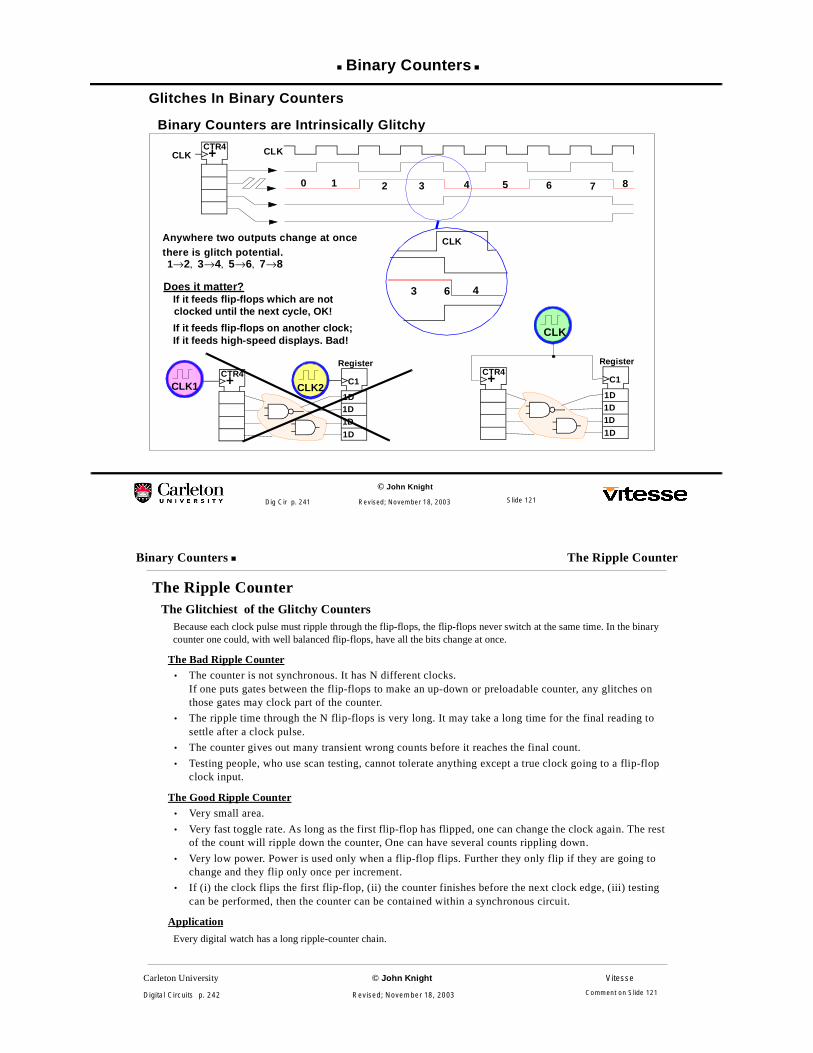
Glitches In Binary Counters
Binary Counters are Intrinsically Glitchy
CLK + CLK
3 6 4
0 1 2 3 4 5 6 7 8
CTR4
CLKAnywhere two outputs change at oncethere is glitch potential.1→2, 3→4, 5→6, 7→8
Does it matter?If it feeds flip-flops which are notclocked until the next cycle, OK!
If it feeds flip-flops on another clock;If it feeds high-speed displays. Bad!
C1
1D1D1D1D
Register
CLK
+CTR4
CLK1 CLK2C1
1D1D1D1D
Register
+CTR4
Slide 121
Carleton University © John Knight Vitesse
Digital Circuits p. 242 Revised; November 18, 2003
Binary Counters The Ripple Counter
The Ripple CounterThe Glitchiest of the Glitchy Counters
Because each clock pulse must ripple through the flip-flops, the flip-flops never switch at the same time. In the binarycounter one could, with well balanced flip-flops, have all the bits change at once.
The Bad Ripple Counter• The counter is not synchronous. It has N different clocks.
If one puts gates between the flip-flops to make an up-down or preloadable counter, any glitches onthose gates may clock part of the counter.
• The ripple time through the N flip-flops is very long. It may take a long time for the final reading tosettle after a clock pulse.
• The counter gives out many transient wrong counts before it reaches the final count.
• Testing people, who use scan testing, cannot tolerate anything except a true clock going to a flip-flopclock input.
The Good Ripple Counter• Very small area.
• Very fast toggle rate. As long as the first flip-flop has flipped, one can change the clock again. The restof the count will ripple down the counter, One can have several counts rippling down.
• Very low power. Power is used only when a flip-flop flips. Further they only flip if they are going tochange and they flip only once per increment.
• If (i) the clock flips the first flip-flop, (ii) the counter finishes before the next clock edge, (iii) testingcan be performed, then the counter can be contained within a synchronous circuit.
Application
Every digital watch has a long ripple-counter chain.
Comment on Slide 121
The Ripple Counter
© John Knight
Dig Cir p. 243 Revised; November 18, 2003
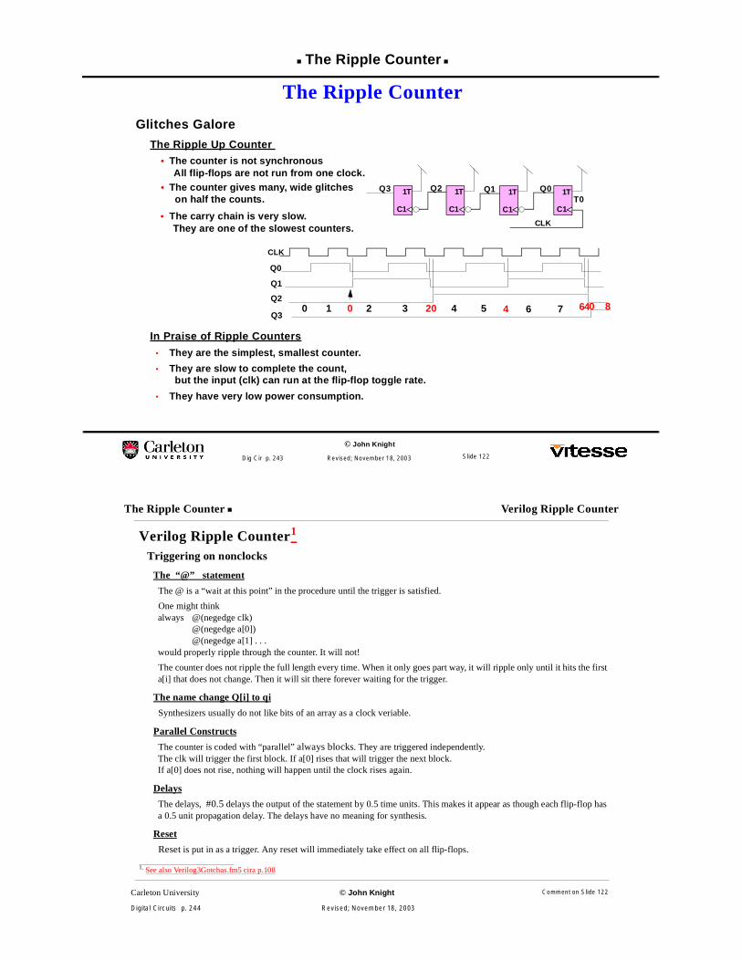
The Ripple Counter
Glitches Galore
The Ripple Up Counter
In Praise of Ripple Counters
• They are the simplest, smallest counter.
• They are slow to complete the count,but the input (clk) can run at the flip-flop toggle rate.
• They have very low power consumption.
1T
C1
CLK
Q0T0
1T
C1
Q11T
C1
Q21T
C1
Q3
CLK
Q0
Q1
Q2
Q3
• The counter is not synchronousAll flip-flops are not run from one clock.
• The counter gives many, wide glitcheson half the counts.
• The carry chain is very slow.
0 1 0 2 3 20 4 5 4 6 7 640 8
They are one of the slowest counters.
Slide 122
Carleton University © John Knight Vitesse
Digital Circuits p. 244 Revised; November 18, 2003
The Ripple Counter Verilog Ripple Counter
Verilog Ripple Counter1
Triggering on nonclocks
The “@” statement
The @ is a “wait at this point” in the procedure until the trigger is satisfied.
One might thinkalways @(negedge clk)
@(negedge a[0])@(negedge a[1] . . .
would properly ripple through the counter. It will not!
The counter does not ripple the full length every time. When it only goes part way, it will ripple only until it hits the firsta[i] that does not change. Then it will sit there forever waiting for the trigger.
The name change Q[i] to qi
Synthesizers usually do not like bits of an array as a clock veriable.
Parallel Constructs
The counter is coded with “parallel” always blocks. They are triggered independently.The clk will trigger the first block. If a[0] rises that will trigger the next block.If a[0] does not rise, nothing will happen until the clock rises again.
Delays
The delays, #0.5 delays the output of the statement by 0.5 time units. This makes it appear as though each flip-flop hasa 0.5 unit propagation delay. The delays have no meaning for synthesis.
Reset
Reset is put in as a trigger. Any reset will immediately take effect on all flip-flops.
1. See also Verilog3Gotchas.fm5 cira p.108
Comment on Slide 122

The Ripple Counter
© John Knight
Dig Cir p. 245 Revised; November 18, 2003
A Verilog Ripple Countermodule rip(Q, clk, reset);
output[n:0] Q; reg [n:0] Q;input clk, reset;wire q0, q1, q2;
Fig. Com 0-1
always @(negedge clk or posedge reset) // negedge for up counterif (reset) Q[0]=0; // posedge for down counter
else begin#0.5 Q[0] = ~Q[0]; // Delay will not synthesize but makes simulation clearer.end
assign q0 = Q[0]; // Subscripted variables cannot be put in trigger lists as clocks.
always @(negedge q0 or posedge reset)if (reset) Q[0]=0;else begin
#0.5 Q[1] = (~Q[1]);end
assign q1 = Q[1];
always @(negedge q1 or posedge reset)if (reset) Q[2]=0;else begin#0.5 Q[2] = (~Q[2]);end
assign q2 = Q[2];. . .
endmodule // rip
Slide 123
Carleton University © John Knight Vitesse
Digital Circuits p. 246 Revised; November 18, 2003
The Ripple Counter Gray Codes
Gray CodesGlitch-Free Counting
Because they change only one bit at a time, Gray code counters are inherently glitch free. This only applies if oneincrements by 1. Counting with increments of 2 or more will give glitches.
Types of Gray Codes
Here we define a Gray code as any code that increments with one bit-change at a time. There are thousands of Graycodes. Tracing through the Karnaugh map will show many. A Johnson Counter gives a Gray code.
The reflected Gray code is the most commonly used Gray code
a. Take the Gray code shown and drop the most significant bit temporarily.
b. Draw a line half way up the list.
c. Think of the line as a mirror. Then the numbers below the line are the reflection of those above.
Wrap-Around Gray Codes
Some Gray codes may not wrap around.
Comment on Slide 123

Gray Code Counters
© John Knight
Dig Cir p. 247 Revised; November 18, 2003
Gray Code Counters
Single Bit-Change Counters• Gray codes are binary encodings of numbers which change only one bit at a time.
• There are many of them.
• Gray codes can be read off a Karnaugh map.
Follow a trace through the Karnaugh map.Write down the squares in the order you pass throughthem.The common reflected Gray code shown(right).
Another Gray code which starts at 0100 and ends at 1111.Follow the map trace and equate these with binary codes.This one is not a Gray code on overflow.
00 01 11 1000
ABCD
01
11
10
0 ≈ 00001 ≈ 00012 ≈ 00113 ≈ 00104 ≈ 01105 ≈ 01116 ≈ 01017 ≈ 01008 ≈ 11009 ≈ 1101
10 ≈ 111111 ≈ 111012 ≈ 101013 ≈ 101114 ≈ 100115 ≈ 100000 01 11 10
00
ABCD
01
11
10
0 ≈ 01001 ≈ 00002 ≈ 00013 ≈ 00114 ≈ 00105 ≈ 01106 ≈ 01117 ≈ 0101
8 ≈ 11019 ≈ 1100
10 ≈ 100011 ≈ 100112 ≈ 101113 ≈ 101014 ≈ 111015 ≈ 1111
Slide 124
Carleton University © John Knight Vitesse
Digital Circuits p. 248 Revised; November 18, 2003
Gray Code Counters Uses Of Gray Code Counters
Uses Of Gray Code CountersAn External Counter Feeding A Synchronous Machine
Overspeed Detector
This detector is reset every second.Starting from zero it counts the number of slots that go by the toothed wheel.If the number of slots goes above the setpoint, the motor is shut down.
It must be manually restarted.
Reliability
Depending on the way the counter glitches, this may erroneously shut down the motor.
For the counter in "Binary Counters are Intrinsically Glitchy," p. 241, a set count of 6 could stop the motor when the realcount was only 4.
This would not happen too often. The clock would have to rise as the counter was glitching.1
1. The ripple counter would not cause a problem here. It can never glitch to a higher number than the actual count.
Comment on Slide 124

Gray Code Counters
© John Knight
Dig Cir p. 249 Revised; November 18, 2003
Uses Of Gray Code Counters
Inputs to Synchronous Systems
Motor Overspeed Control.The binary counter counts sensor pulses for 1 second.The count is compared with the setpoint register. Set a MAX(pulses/sec)If ω > s a STOP signal is sent out.
The motor stops when there is no overspeed.
Suggest some problems and their cures.
CounterBinary Set point
Register
Write
Digital Compareω>s
ω s10
R
stopCount is maximum
10
clk
C1
Next clock cycleclear binarycounter
at the end of each
SynchronousController
R
RESET
1DC1
second.
OVERSPEED
Slide 125
Carleton University © John Knight Vitesse
Digital Circuits p. 250 Revised; November 18, 2003
Gray Code Counters A Brute-Force Gray-Code Counter
A Brute-Force Gray-Code CounterCoding By Next-State
A Finite-state Machine As a Case Statement
a. Enter the present state as the test in a case statement
b. Enter the next state as the result.
A Finite-state Machine As an Excessive Case Statement
A 10 bit counter will have 1024 entries; a 20 bit counter will have 104857 entries. Too much!
5 or 6 flip-flops appear to be a practical limit.
The Alternative To Brute Force; Finite-State Machine (FSM) CodingState Table For Gray Code.
T
State Nxt St D Inputs T Inputs State Nxt St D Inputs T InputsQ3Q2Q1Q0 Q3
+Q2+Q1
+Q0 D3D2D1D0 T3T2T1T0 Q3Q2Q1Q0 Q3+Q2
+Q1+Q0 D3D2D1D0 T3T2T1T0
0000 0001 0001 - - - t 1100 1101 0001 - - - t
0001 0011 0011 - - t - 1101 1111 0011 - - t -
0011 0010 0010 - - - t 1111 1110 0010 - - - t
0010 0110 0110 - t - - 1110 1010 0110 - t - -
0110 0111 0111 - - - t 1010 1001 0111 - - - t
0111 0101 0101 - - t - 1001 1001 0101 - - t -
0101 0100 0100 - - - t 1001 1000 0100 - - - t
0100 1100 1100 t - - - 1000 0000 1100 t - - -
Comment on Slide 125

Gray Code Counters
© John Knight
Dig Cir p. 251 Revised; November 18, 2003
Gray Code Counter
always @(posedge reset or posedge clock)if (reset) Q <= 0;else
case (Q)3'b000: Q <= 3'b001;3'b001: Q <= 3'b011;3'b011: Q <= 3'b010;3'b010: Q <= 3'b110;3'b110: Q <= 3'b111;3'b111: Q <= 3'b101;3'b101: Q <= 3'b100;3'b100: Q <= 3'b000;default: Q <= 3'bx;
endcase
An O( 2N) DescriptionThe size of this table goes up with the square of the number N of flip-flops.
• The synthesizer may increase the circuit as O(2N).
• Certainly the work to enter will increase as O(2N).
Avoid such descriptions if possible.
Step after Reset
(in binary) Gray Code
000 000
001 001
010 011
011 010
100 110
101 111
110 101
111 100
Slide 126
Carleton University © John Knight Vitesse
Digital Circuits p. 252 Revised; November 18, 2003
Gray Code Counters Finite-State Machine (FSM) Coding for
Finite-State Machine (FSM) Coding for Gray-Code CountersMaps for D, T and enabled D flip-flops
D3=Q2 En3=Q1Q0 D2=Q3 En2=Q1Q0 D1=(Q3⊕Q2) En1=Q0 D0=(~(Q3⊕Q2⊕Q1)) En0=1
Map of D3 for flip-flop 3 Map of D2 for flip-flop 2 Map of D1 for flip-flop 1 Map of D0 for flip-flop 0
Q3Q2\Q1Q0
00 01 11 10Q3Q2\
Q1Q0
00 01 11 10Q3Q2\
Q1Q0
00 01 11 10Q3Q2\
Q1Q0
00 01 11 1000 0 0 0 0 00 0 0 0 1 00 0 1 1 1 00 1 1 0 001 1 0 0 0 01 1 1 1 1 01 0 0 0 1 01 0 0 1 111 1 1 1 1 11 1 1 1 0 11 0 1 1 1 11 1 1 0 010 0 1 1 1 10 0 0 0 0 10 0 0 0 1 10 0 0 1 1
D3=Q2Q1Q0+(Q1+Q0)Q3 D2=Q3Q1Q0+(Q1+Q0)Q2 D1=(~(Q3⊕Q2))Q0+Q1Q0 D0=(~(Q3⊕Q2⊕Q1))
Map of T3 for flip-flop 3 Map of T2 for flip-flop 2 Map of T1 for flip-flop 1 Map of T0 for flip-flop 0
Q3Q2\Q1Q0
00 01 11 10Q3Q2\
Q1Q0
00 01 11 10Q3Q2\
Q1Q0
00 01 11 10Q3Q2\
Q1Q0
00 01 11 1000 0 0 0 0 00 0 0 0 t 00 0 t 0 0 00 t 0 t 001 t 0 0 0 01 0 0 0 0 01 0 0 t 0 01 0 t 0 t11 0 0 0 0 11 0 0 0 t 11 0 t 0 0 11 t 0 t 010 t 0 0 0 10 0 0 0 0 10 0 0 t 0 10 0 t 0 t
T3=(Q3⊕Q2)Q1Q0 T2=(~(Q3⊕Q2))Q1Q0 T1=(~(Q3⊕Q2⊕Q1)Q0) T0=(~(Q3⊕Q2⊕Q1⊕Q0))
Map of D3 and En 3 Map of D2 and En 2 Map of D1 and En 1 Map of D0 and En 0
Q3Q2\Q1Q0
00 01 11 10Q3Q2\
Q1Q0
00 01 11 10Q3Q2\
Q1Q0
00 01 11 10Q3Q2\
Q1Q0
00 01 11 1000 0 d d d 00 d d d 1 00 d 1 1 d 00 1 1 0 001 1 d d d 01 d d d 1 01 d 0 0 d 01 0 0 1 111 1 d d d 11 d d d 0 11 d 1 1 d 11 1 1 0 010 0 d d d 10 d d d 0 10 d 0 0 d 10 0 0 1 1
Comment on Slide 126
Gray Code Counters
© John Knight
Dig Cir p. 253 Revised; November 18, 2003
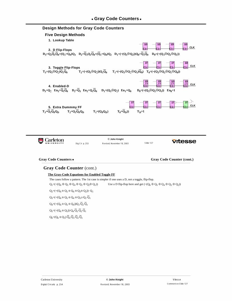
Design Methods for Gray Code Counters
Five Design Methods1. Lookup Table
2. D Flip-FlopsD3=Q2Q1Q0+(Q1+Q0)Q3 D2=Q3Q1Q0+(Q1+Q0)Q2 D1=(~(Q3⊕Q2))Q0+Q1Q0 D0=(~(Q3⊕Q2⊕Q1))
3. Toggle Flip-FlopsT3=(Q3⊕Q2)Q1Q0 T2=(~(Q3⊕Q2))Q1Q0 T1=(~(Q3⊕Q2⊕Q1)Q0) T0=(~(Q3⊕Q2⊕Q1⊕Q0))
4. Enabled-DD3=Q2 En3=Q1Q0 D2=Q3 En2=Q1Q0 D1=(Q3⊕Q2) En1=Q0 D0=(~(Q3⊕Q2⊕Q1)) En0=1
5. Extra Dummmy FFT3=Q1Q0QD T2=Q1Q0QD T1=(Q0QD) T0=QD)) TD=1
1D
C1 CLK1D
C1
1D
C1
1D
C1
1D
C1 CLK1T
C1
1T
C1
1T
C1
1D
C1 CLK1D
C1
1D
C1
1D
C1EN EN ENEN
1T
C1 CLK1T
C1
1T
C1
1T
C1
1T
C1
Slide 127
Carleton University © John Knight Vitesse
Digital Circuits p. 254 Revised; November 18, 2003
Gray Code Counters Gray Code Counter (cont.)
Gray Code Counter (cont.)
The Gray-Code Equations for Enabled Toggle FF
The cases follow a pattern. The 1st case is simpler if one uses a D, not a toggle, flip-flop.
Q1=(~(Q6 ⊕ Q5 ⊕ Q4 ⊕ Q3 ⊕ Q2⊕ Q1)) Use a D flip-flop here and get (~(Q6 ⊕ Q5 ⊕ Q4 ⊕ Q3 ⊕ Q2))
Q2=(~(Q6 ⊕ Q5 ⊕ Q4 ⊕ Q3⊕ Q2))· Q1
Q3=(~(Q6 ⊕ Q5 ⊕ Q4 ⊕ Q3))·Q2·Q1
Q4=(~(Q6 ⊕ Q5 ⊕ Q4))Q3·Q2·Q1
Q5=(~(Q6 ⊕ Q5))·Q4·Q3·Q2·Q1
Q6=(Q6 ⊕ Q5)·Q4·Q3·Q2·Q1
Comment on Slide 127

Gray Code Counters
© John Knight
Dig Cir p. 255 Revised; November 18, 2003
Complicated Gray
module Gray(Q, clk, reset);parameter n=6; / / Number of T flip-flops
output[n:1]Q; reg [n:1]Q; / / Register all procedure outputs.input clk, reset;
always @(posedge clk or posedge reset)if (reset) Q<=0;
else begin
/ / Q[1] <= (Q 6⊕Q5⊕Q4⊕Q3⊕Q2); / / ←This one is a D -FF.Q[1] <= (~(^Q[n:2]));
/ / Toggle FF statements
/ / Q2 <= IF ( (Q6⊕Q5⊕Q4⊕Q 3⊕Q2)& Q1) THEN Q2 : ELSE Q2;Q[2] <= (~(^Q[n:2])&Q[1]) ? ~Q[2] : Q[2];
/ / Q3 <= IF (Q6⊕Q5⊕Q4⊕Q 3)&Q 2&(~ Q1) ) THEN Q3 : ELSE Q3;Q[3] <= (~(̂ Q[n:3]))&Q[2]&(~|Q[1]) ? ~Q[3] : Q[3];
/ / Q4 <= IF(Q6⊕Q5⊕Q4)&Q3&Q2&Q1) THEN Q4 : ELSE Q4;Q[4] <= (~(̂ Q[n:4]))&Q[n-3]&(~|Q[n-4:1]) ? ~Q[4] : Q[4];
/ / Q5 <= IF( (Q6⊕Q5)&Q4&Q3 &Q2& Q1) THEN Q5 : ELSE Q5;Q[5] <= (~(̂ Q[n:5]))&Q[n-2]&(~|Q[n-3:1]) ? ~Q[5] : Q[5];
/ / Q6 <=IF (Q6⊕Q5)& Q4& Q3&Q 2&Q1) THEN Q6 : ELSE Q6;Q[6] <= (̂ Q[n:5])&(~|Q[n-2:1]) ? ~Q[6] : Q[6];
end / / elseendmodule / / Gray
Slide 128
Carleton University © John Knight Vitesse
Digital Circuits p. 256 Revised; November 18, 2003
Gray Code Counters The Gray-Code With Dummy Toggle FF
The Gray-Code With Dummy Toggle FFThe logic can be greatly simplified by adding a dummy flip-flop, QD, which toggles every cycle.
Since Q0 toggles every 2nd cycle, its toggle can be controlled directly from QD.
The controls for the other bit simplify as shown below..
Reference:Altera Application Brief 135, Ripple-Carry Gray-Code Counters, Altera Corp, May 1994.
T
State Dum T Inputs Toggle to State Dum T Inputs Toggle toQ3Q2Q1Q0 QD T3T2T1T0 give next state Q3Q2Q1Q0 QD T3T2T1T0 give next state
0 0 0 0 0 - - - t T0=QD 1 1 0 0 0 - - - t T0=QD
0 0 0 1 1 - - t - T1=Q0QD 1 1 0 1 1 - - t - T1=Q1QD
0 0 1 1 0 - - - t T0=QD 1 1 1 1 0 - - - t T0=QD
0 0 1 0 1 - t - - T2=Q1Q0QD 1 1 1 0 1 - t - - T2=Q2Q1QD
0 1 1 0 0 - - - t T0=QD 1 0 1 0 0 - - - t T0=QD
0 1 1 1 1 - - t - T1=Q0QD 1 0 1 1 1 - - t - T1=Q1QD
0 1 0 1 0 - - - t T0=QD 1 0 0 1 0 - - - t T0=QD
0 1 0 0 1 t - - - T3=Q1Q0QD 1 0 0 0 1 t - - - T3=Q1Q0QD
Comment on Slide 128

Gray Code Counters
© John Knight
Dig Cir p. 257 Revised; November 18, 2003
Extra FF Gray Code counter
T Flip-Flops Circuit(Simplest for People)
The T table shows where the bitstoggle between the present stateand the next state.
The circles show how the togglesignals are defined by zeros:
c
Present State Next State What to ToggleQ3 Q2 Q1 Q0 Qd Q3 Q2 Q1 Q0 Qd T3 T2 T1 T0 Td
0 0 0 0 0 0 0 0 1 1 T T
0 0 0 1 1 0 0 1 1 0 T T
0 0 1 1 0 0 0 1 0 1 T T
0 0 1 0 1 0 1 1 0 0 T T
0 1 1 0 0 0 1 1 1 1 T T
0 1 1 1 1 0 1 0 1 0 T T
0 1 0 1 0 0 1 0 0 1 T T
0 1 0 0 1 1 1 0 0 0 T T
1 1 0 0 0 1 1 0 1 1 T T
1 1 0 1 1 1 1 1 1 0 T T
1 1 1 1 0 1 1 1 0 1 T T
1 1 1 0 1 1 0 1 0 0 T T
1 0 1 0 0 1 0 1 1 1 T T
1 0 1 1 1 1 0 0 1 0 T T
1 0 0 1 0 1 0 0 0 1 T T
1 0 0 0 1 0 0 0 0 0 T T
0 0 0 0 0 0 0 0 1 1 T T
0 0 0 1 0 0 0 0 T T
Td = 1T0 = QdT1 = Q0QdT2 = Q1Q0QdT3 = Q1Q0Qd
Slide 129
Carleton University © John Knight Vitesse
Digital Circuits p. 258 Revised; November 18, 2003
Gray Code Counters The Gray-Code With Dummy Toggle FF
The Most-Significant BitIn Gray codes the most significant bit is not symmetric with the others.This is why the expression for Q3 on “Extra FF Gray Code counter” on page 257 does not match "Verilog Extra Flip-Flop Gray-Code Counter," p. 259
Fake Gray CodeA Binary counter can be converted to output Gray code by placing an XOR between each pair of its bits:... G2=B3⊕B2, G1=B2⊕B1, G0=B1⊕B0.
Unfortunately the glitches in the original binary counter will come through and give a “glitchy Gray Code” output.
Comment on Slide 129

Gray Code Counters
© John Knight
Dig Cir p. 259 Revised; November 18, 2003
Verilog Extra Flip-Flop Gray-Code Counter
module SimplGray(Q, clk, reset);parameter n=6; // Number of T flip-flops
output[n:1]Q; reg [n:1]Q; // Register all procedure outputs.input clk, reset;
reg Qd;
always @(posedge clk or posedge reset)beginif (reset) Begin Q<=0; Qd<0; end
else begin
// Toggle FF statementsQd <= ~Qd;
Q[0] <= (~Qd) ? ~Q[0] : Q[0];
Q[1] <= ({Q[0],Qd}= =2’b11) ? ~Q[1] : Q[1];Q[2] <= ({Q[1:0],Qd}= =3’b101) ? ~Q[2] : Q[2];
Q[3] <= ({Q[1:0],Qd}= =4’b1001) ? ~Q[3] : Q[3];
Q[4] <= ({Q[3:0],Qd}= =5’b10001) ? ~Q[4] : Q[4];
Q[5] <= ({Q[4:0],Qd}= =6’b100001) ? ~Q[5] : Q[5]; WRONG FOR END
end // else
end //begin for alwaysendmodule //SimplGray
Slide 130
Carleton University © John Knight Vitesse
Digital Circuits p. 260 Revised; November 18, 2003
Gray Code Counters The Gray-Code With Dummy Toggle FF
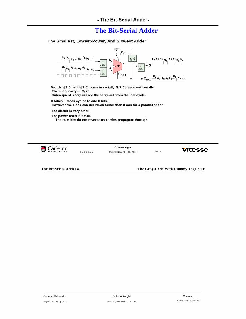
The Bit-Serial Adder• This adder adds one bit per clock cycle.
It adds strings of bits coming in serially and sends out the result as a serial stream.
• An 8-bit ripple-carry adder takes 8 carry propagation delays to add.
• An 8-bit serial adder need only wait formax(carry output, sum output)
in each clock cycle.However it takes eight clock cycles.
• The 8-bit, bit-serial adder is slower than an 8-bit parallel adder, but not 8 times slower since (or if) theclock can be made faster.
Comment on Slide 130
The Bit-Serial Adder
© John Knight
Dig Cir p. 261 Revised; November 18, 2003
The Bit-Serial Adder
The Smallest, Lowest-Power, And Slowest Adder
Words a[7:0] and b[7:0] come in serially. S[7:0] feeds out serially.The initial carry-in C0=0.Subsequent carry-ins are the carry-out from the last cycle.
It takes 8 clock cycles to add 8 bits.However the clock can run much faster than it can for a parallel adder.
The circuit is very small.
The power used is small.The sum bits do not reverse as carries propagate through.
a
bS
Cn+1
1DC1
1DC1
1DC1
“0”
Cn+1
S
b0
a1a2a3a4
a5a6a7
a0
b1b2b3b4b5
b6b7 s0s1s2s3s4
s5s6s7
c0c1c2c3c4c5
c7 c6
+
Cn
1D C1
Slide 131
Carleton University © John Knight Vitesse
Digital Circuits p. 262 Revised; November 18, 2003
The Bit-Serial Adder The Gray-Code With Dummy Toggle FF
Comment on Slide 131
Related Documents