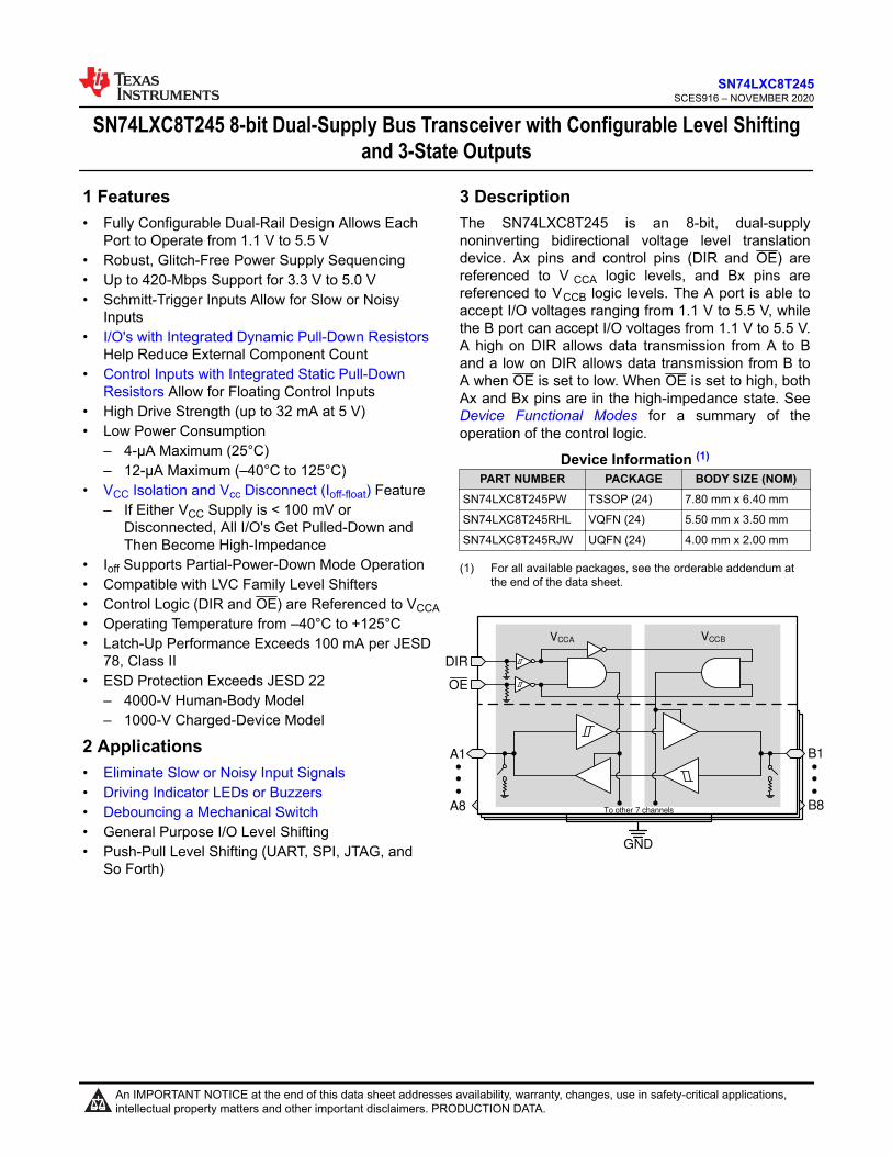
SN74LXC8T245 8-bit Dual-Supply Bus Transceiver with Configurable Level Shifting and 3-State Outputs 1 Features • Fully Configurable Dual-Rail Design Allows Each Port to Operate from 1.1 V to 5.5 V • Robust, Glitch-Free Power Supply Sequencing • Up to 420-Mbps Support for 3.3 V to 5.0 V • Schmitt-Trigger Inputs Allow for Slow or Noisy Inputs • I/O's with Integrated Dynamic Pull-Down Resistors Help Reduce External Component Count • Control Inputs with Integrated Static Pull-Down Resistors Allow for Floating Control Inputs • High Drive Strength (up to 32 mA at 5 V) • Low Power Consumption – 4-µA Maximum (25°C) – 12-µA Maximum (–40°C to 125°C) • V CC Isolation and V cc Disconnect (I off-float ) Feature – If Either V CC Supply is < 100 mV or Disconnected, All I/O's Get Pulled-Down and Then Become High-Impedance • I off Supports Partial-Power-Down Mode Operation • Compatible with LVC Family Level Shifters • Control Logic (DIR and OE) are Referenced to V CCA • Operating Temperature from –40°C to +125°C • Latch-Up Performance Exceeds 100 mA per JESD 78, Class II • ESD Protection Exceeds JESD 22 – 4000-V Human-Body Model – 1000-V Charged-Device Model 2 Applications • Eliminate Slow or Noisy Input Signals • Driving Indicator LEDs or Buzzers • Debouncing a Mechanical Switch • General Purpose I/O Level Shifting • Push-Pull Level Shifting (UART, SPI, JTAG, and So Forth) 3 Description The SN74LXC8T245 is an 8-bit, dual-supply noninverting bidirectional voltage level translation device. Ax pins and control pins (DIR and OE) are referenced to V CCA logic levels, and Bx pins are referenced to V CCB logic levels. The A port is able to accept I/O voltages ranging from 1.1 V to 5.5 V, while the B port can accept I/O voltages from 1.1 V to 5.5 V. A high on DIR allows data transmission from A to B and a low on DIR allows data transmission from B to A when OE is set to low. When OE is set to high, both Ax and Bx pins are in the high-impedance state. See Device Functional Modes for a summary of the operation of the control logic. Device Information (1) PART NUMBER PACKAGE BODY SIZE (NOM) SN74LXC8T245PW TSSOP (24) 7.80 mm x 6.40 mm SN74LXC8T245RHL VQFN (24) 5.50 mm x 3.50 mm SN74LXC8T245RJW UQFN (24) 4.00 mm x 2.00 mm (1) For all available packages, see the orderable addendum at the end of the data sheet. A8 B8 A1 B1 OE DIR V CCA V CCB To other 7 channels GND www.ti.com SN74LXC8T245 SCES916 – NOVEMBER 2020 Copyright © 2020 Texas Instruments Incorporated Submit Document Feedback 1 Product Folder Links: SN74LXC8T245 SN74LXC8T245 SCES916 – NOVEMBER 2020 An IMPORTANT NOTICE at the end of this data sheet addresses availability, warranty, changes, use in safety-critical applications, intellectual property matters and other important disclaimers. PRODUCTION DATA.

Welcome message from author
This document is posted to help you gain knowledge. Please leave a comment to let me know what you think about it! Share it to your friends and learn new things together.
Transcript
SN74LXC8T245 8-bit Dual-Supply Bus Transceiver with Configurable Level Shiftingand 3-State Outputs
1 Features• Fully Configurable Dual-Rail Design Allows Each
Port to Operate from 1.1 V to 5.5 V• Robust, Glitch-Free Power Supply Sequencing• Up to 420-Mbps Support for 3.3 V to 5.0 V• Schmitt-Trigger Inputs Allow for Slow or Noisy
Inputs• I/O's with Integrated Dynamic Pull-Down Resistors
Help Reduce External Component Count• Control Inputs with Integrated Static Pull-Down
Resistors Allow for Floating Control Inputs• High Drive Strength (up to 32 mA at 5 V)• Low Power Consumption
– 4-µA Maximum (25°C)– 12-µA Maximum (–40°C to 125°C)
• VCC Isolation and Vcc Disconnect (Ioff-float) Feature– If Either VCC Supply is < 100 mV or
Disconnected, All I/O's Get Pulled-Down andThen Become High-Impedance
• Ioff Supports Partial-Power-Down Mode Operation• Compatible with LVC Family Level Shifters• Control Logic (DIR and OE) are Referenced to VCCA• Operating Temperature from –40°C to +125°C• Latch-Up Performance Exceeds 100 mA per JESD
78, Class II• ESD Protection Exceeds JESD 22
– 4000-V Human-Body Model– 1000-V Charged-Device Model
2 Applications• Eliminate Slow or Noisy Input Signals• Driving Indicator LEDs or Buzzers• Debouncing a Mechanical Switch• General Purpose I/O Level Shifting• Push-Pull Level Shifting (UART, SPI, JTAG, and
So Forth)
3 DescriptionThe SN74LXC8T245 is an 8-bit, dual-supplynoninverting bidirectional voltage level translationdevice. Ax pins and control pins (DIR and OE) arereferenced to V CCA logic levels, and Bx pins arereferenced to VCCB logic levels. The A port is able toaccept I/O voltages ranging from 1.1 V to 5.5 V, whilethe B port can accept I/O voltages from 1.1 V to 5.5 V.A high on DIR allows data transmission from A to Band a low on DIR allows data transmission from B toA when OE is set to low. When OE is set to high, bothAx and Bx pins are in the high-impedance state. SeeDevice Functional Modes for a summary of theoperation of the control logic.
Device Information (1)
PART NUMBER PACKAGE BODY SIZE (NOM)SN74LXC8T245PW TSSOP (24) 7.80 mm x 6.40 mm
SN74LXC8T245RHL VQFN (24) 5.50 mm x 3.50 mm
SN74LXC8T245RJW UQFN (24) 4.00 mm x 2.00 mm
(1) For all available packages, see the orderable addendum atthe end of the data sheet.
A8 B8
A1 B1
OE
DIR
VCCA VCCB
To other 7 channels
GND
www.ti.comSN74LXC8T245
SCES916 – NOVEMBER 2020
Copyright © 2020 Texas Instruments Incorporated Submit Document Feedback 1
Product Folder Links: SN74LXC8T245
SN74LXC8T245SCES916 – NOVEMBER 2020
An IMPORTANT NOTICE at the end of this data sheet addresses availability, warranty, changes, use in safety-critical applications,intellectual property matters and other important disclaimers. PRODUCTION DATA.

Table of Contents1 Features............................................................................12 Applications..................................................................... 13 Description.......................................................................14 Revision History.............................................................. 25 Pin Configuration and Functions...................................36 Specifications.................................................................. 4
6.1 Absolute Maximum Ratings ....................................... 46.2 ESD Ratings .............................................................. 46.3 Recommended Operating Conditions ........................56.4 Thermal Information ...................................................56.5 Electrical Characteristics ............................................66.6 Switching Characteristics, VCCA = 1.2 ± 0.1 V............ 96.7 Switching Characteristics, VCCA = 1.5 ± 0.1 V.......... 106.8 Switching Characteristics, VCCA = 1.8 ± 0.15 V........ 116.9 Switching Characteristics, VCCA = 2.5 ± 0.2 V.......... 126.10 Switching Characteristics, VCCA = 3.3 ± 0.3 V........ 136.11 Switching Characteristics, VCCA = 5.0 ± 0.5 V........ 146.12 Switching Characteristics: Tsk, TMAX ......................156.13 Operating Characteristics ...................................... 156.14 Typical Characteristics............................................ 16
7 Parameter Measurement Information.......................... 177.1 Load Circuit and Voltage Waveforms........................17
8 Detailed Description......................................................198.1 Overview................................................................... 198.2 Functional Block Diagram......................................... 198.3 Feature Description...................................................208.4 Device Functional Modes..........................................22
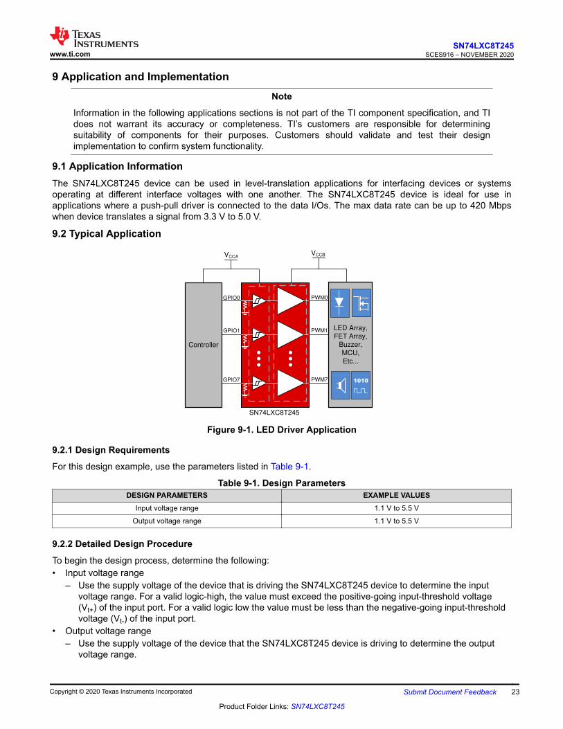
9 Application and Implementation.................................. 239.1 Application Information............................................. 239.2 Typical Application.................................................... 23
10 Power Supply Recommendations..............................2411 Layout...........................................................................24
11.1 Layout Guidelines................................................... 2411.2 Layout Example...................................................... 24
12 Device and Documentation Support..........................2512.1 Device Support....................................................... 2512.2 Receiving Notification of Documentation Updates..2512.3 Support Resources................................................. 2512.4 Trademarks.............................................................2512.5 Electrostatic Discharge Caution..............................2512.6 Glossary..................................................................25
13 Mechanical, Packaging, and OrderableInformation.................................................................... 26
4 Revision HistoryNOTE: Page numbers for previous revisions may differ from page numbers in the current version.
DATE REVISION NOTESNovember 2020 * Initial Release
SN74LXC8T245SCES916 – NOVEMBER 2020 www.ti.com
2 Submit Document Feedback Copyright © 2020 Texas Instruments Incorporated
Product Folder Links: SN74LXC8T245
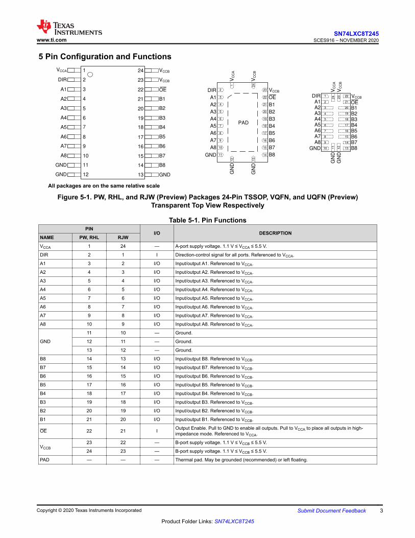
5 Pin Configuration and Functions1
2
3
4
5
6
7
8
9
10
11
12
24
23
22
21
20
19
18
17
16
15
14
13
VCCB
DIR
A1
A2
A3
A4
A5
A6
A7
A8
GND
GND
B1
B2
B3
B4
B5
B6
B7
B8
GND
VCCB
OE
VCCA
24
23
22
21
20
19
18
17
16
15
14
12
13
2
3
4
5
6
7
8
9
10
11
PAD
1
DIR
A1
A2
A3
A4
A5
A6
A7
A8
GND
GN
DV
CC
A
VC
CB
VCCB
GN
D
B1
B2
B3
B4
B5
B6
B7
B8
OE 241
2
3
4
23
5
6
7
8
9
10 11
12
13
14
15
16
17
18
19
20
21
22 VCCB
B1
B2
B3
B4
B5
B6
B7
B8
OE
VC
CA
VC
CB
GN
D
GN
D
DIR
A1
A2
A3
A4
A5
A6
A7
A8
GND
All packages are on the same relative scale
Figure 5-1. PW, RHL, and RJW (Preview) Packages 24-Pin TSSOP, VQFN, and UQFN (Preview)Transparent Top View Respectively
Table 5-1. Pin FunctionsPIN
I/O DESCRIPTIONNAME PW, RHL RJW
VCCA 1 24 — A-port supply voltage. 1.1 V ≤ VCCA ≤ 5.5 V.
DIR 2 1 I Direction-control signal for all ports. Referenced to VCCA.
A1 3 2 I/O Input/output A1. Referenced to VCCA.
A2 4 3 I/O Input/output A2. Referenced to VCCA.
A3 5 4 I/O Input/output A3. Referenced to VCCA.
A4 6 5 I/O Input/output A4. Referenced to VCCA.
A5 7 6 I/O Input/output A5. Referenced to VCCA.
A6 8 7 I/O Input/output A6. Referenced to VCCA.
A7 9 8 I/O Input/output A7. Referenced to VCCA.
A8 10 9 I/O Input/output A8. Referenced to VCCA.
GND
11 10 — Ground.
12 11 — Ground.
13 12 — Ground.
B8 14 13 I/O Input/output B8. Referenced to VCCB.
B7 15 14 I/O Input/output B7. Referenced to VCCB.
B6 16 15 I/O Input/output B6. Referenced to VCCB.
B5 17 16 I/O Input/output B5. Referenced to VCCB.
B4 18 17 I/O Input/output B4. Referenced to VCCB.
B3 19 18 I/O Input/output B3. Referenced to VCCB.
B2 20 19 I/O Input/output B2. Referenced to VCCB.
B1 21 20 I/O Input/output B1. Referenced to VCCB.
OE 22 21 I Output Enable. Pull to GND to enable all outputs. Pull to VCCA to place all outputs in high-impedance mode. Referenced to VCCA.
VCCB23 22 — B-port supply voltage. 1.1 V ≤ VCCB ≤ 5.5 V.
24 23 — B-port supply voltage. 1.1 V ≤ VCCB ≤ 5.5 V.
PAD — — — Thermal pad. May be grounded (recommended) or left floating.
www.ti.comSN74LXC8T245
SCES916 – NOVEMBER 2020
Copyright © 2020 Texas Instruments Incorporated Submit Document Feedback 3
Product Folder Links: SN74LXC8T245
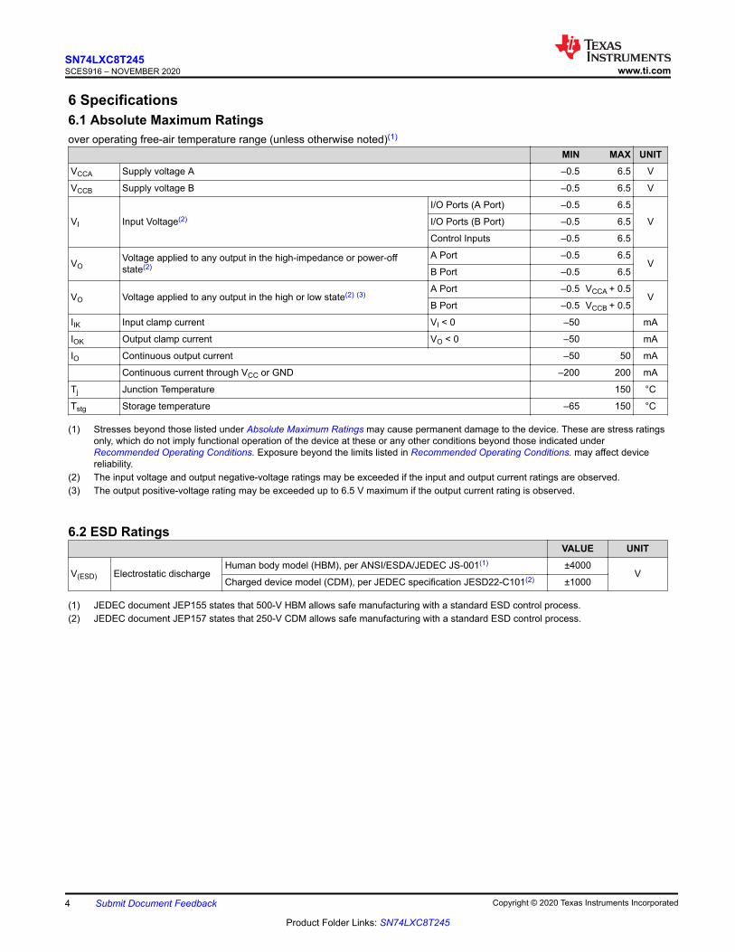
6 Specifications6.1 Absolute Maximum Ratingsover operating free-air temperature range (unless otherwise noted)(1)
MIN MAX UNITVCCA Supply voltage A –0.5 6.5 V
VCCB Supply voltage B –0.5 6.5 V
VI Input Voltage(2)
I/O Ports (A Port) –0.5 6.5
VI/O Ports (B Port) –0.5 6.5
Control Inputs –0.5 6.5
VOVoltage applied to any output in the high-impedance or power-offstate(2)
A Port –0.5 6.5V
B Port –0.5 6.5
VO Voltage applied to any output in the high or low state(2) (3)A Port –0.5 VCCA + 0.5
VB Port –0.5 VCCB + 0.5
IIK Input clamp current VI < 0 –50 mA
IOK Output clamp current VO < 0 –50 mA
IO Continuous output current –50 50 mA
Continuous current through VCC or GND –200 200 mA
Tj Junction Temperature 150 °C
Tstg Storage temperature –65 150 °C
(1) Stresses beyond those listed under Absolute Maximum Ratings may cause permanent damage to the device. These are stress ratingsonly, which do not imply functional operation of the device at these or any other conditions beyond those indicated underRecommended Operating Conditions. Exposure beyond the limits listed in Recommended Operating Conditions. may affect devicereliability.
(2) The input voltage and output negative-voltage ratings may be exceeded if the input and output current ratings are observed.(3) The output positive-voltage rating may be exceeded up to 6.5 V maximum if the output current rating is observed.
6.2 ESD RatingsVALUE UNIT
V(ESD) Electrostatic dischargeHuman body model (HBM), per ANSI/ESDA/JEDEC JS-001(1) ±4000
VCharged device model (CDM), per JEDEC specification JESD22-C101(2) ±1000
(1) JEDEC document JEP155 states that 500-V HBM allows safe manufacturing with a standard ESD control process.(2) JEDEC document JEP157 states that 250-V CDM allows safe manufacturing with a standard ESD control process.
SN74LXC8T245SCES916 – NOVEMBER 2020 www.ti.com
4 Submit Document Feedback Copyright © 2020 Texas Instruments Incorporated
Product Folder Links: SN74LXC8T245

6.3 Recommended Operating Conditionsover operating free-air temperature range (unless otherwise noted) (1) (2) (3)
MIN MAX UNITVCCA Supply voltage A 1.1 5.5 V
VCCB Supply voltage B 1.1 5.5 V
IOH High-level output current
VCCO = 1.1 V –0.1
mA
VCCO = 1.4 V –2
VCCO = 1.65 V –4
VCCO = 2.3 V –12
VCCO = 3 V –24
VCCO = 4.5 V –32
IOL Low-level output current
VCCO = 1.1 V 0.1
mA
VCCO = 1.4 V 2
VCCO = 1.65 V 4
VCCO = 2.3 V 12
VCCO = 3 V 24
VCCO = 4.5 V 32
VI Input voltage (3) 0 5.5 V
VO Output voltageActive State 0 VCCO VTri-State 0 5.5
TA Operating free-air temperature –40 125 °C
(1) VCCI is the VCC associated with the input port.(2) VCCO is the VCC associated with the output port.(3) All control inputs and data I/Os of this device have weak pulldowns to ensure the line is not floating when undefined external to the
device. The input leakage from these weak pulldowns is defined by the II specification indicated under Electrical Characteristics.
6.4 Thermal Information
THERMAL METRIC(1)
SN74LXC8T245UNITPW (TSSOP) RHL (VQFN) RJW (UQFN)
24 PINS 24 PINS 24 PINSRθJA Junction-to-ambient thermal resistance 99.6 47.4 TBD °C/W
RθJC(top) Junction-to-case (top) thermal resistance 43.7 42.6 TBD °C/W
RθJB Junction-to-board thermal resistance 54.7 25.1 TBD °C/W
YJT Junction-to-top characterization parameter 6.4 2.7 TBD °C/W
YJBJunction-to-board characterizationparameter 54.3 25.1 TBD °C/W
RθJC(bottom)Junction-to-case (bottom) thermalresistance N/A 14.9 TBD °C/W
(1) For more information about traditional and new thermal metrics, see the Semiconductor and IC Package Thermal Metrics applicationreport.
www.ti.comSN74LXC8T245
SCES916 – NOVEMBER 2020
Copyright © 2020 Texas Instruments Incorporated Submit Document Feedback 5
Product Folder Links: SN74LXC8T245

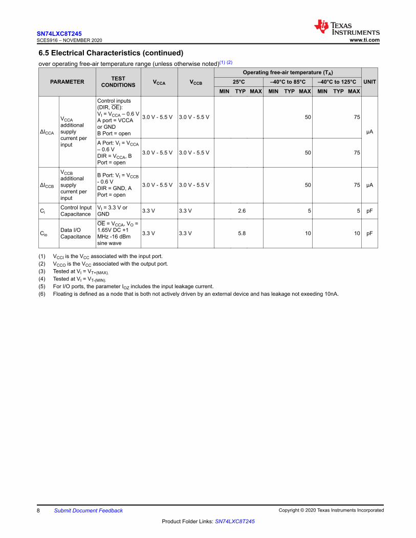
6.5 Electrical Characteristicsover operating free-air temperature range (unless otherwise noted)(1) (2)
PARAMETER TESTCONDITIONS VCCA VCCB
Operating free-air temperature (TA)UNIT25°C –40°C to 85°C –40°C to 125°C
MIN TYP MAX MIN TYP MAX MIN TYP MAX
VT+
Positive-going input-thresholdvoltage
Data Inputs(Ax, Bx)(Referenced toVCCI)
1.1 V 1.1 V 0.44 0.88 0.44 0.88
V
1.4 V 1.4 V 0.60 0.98 0.60 0.98
1.65 V 1.65 V 0.76 1.13 0.76 1.13
2.3 V 2.3 V 1.08 1.56 1.08 1.56
3 V 3 V 1.48 1.92 1.48 1.92
4.5 V 4.5 V 2.19 2.74 2.19 2.74
5.5 V 5.5 V 2.65 3.33 2.65 3.33
Control Inputs(OE, DIR)(Referenced toVCCA)
1.1 V 1.1 V 0.44 0.88 0.44 0.88
V
1.4 V 1.4 V 0.60 0.98 0.60 0.98
1.65 V 1.65 V 0.76 1.13 0.76 1.13
2.3 V 2.3 V 1.08 1.56 1.08 1.56
3 V 3 V 1.48 1.92 1.48 1.92
4.5 V 4.5 V 2.19 2.74 2.19 2.74
5.5 V 5.5 V 2.65 3.33 2.65 3.33
VT-
Negative-going input-thresholdvoltage
Data Inputs(Ax, Bx)(Referenced toVCCI)
1.1 V 1.1 V 0.17 0.48 0.17 0.48
V
1.4 V 1.4 V 0.28 0.59 0.28 0.59
1.65 V 1.65 V 0.35 0.69 0.35 0.69
2.3 V 2.3 V 0.56 0.97 0.56 0.97
3 V 3 V 0.89 1.5 0.89 1.5
4.5 V 4.5 V 1.51 1.97 1.51 1.97
5.5 V 5.5 V 1.88 2.4 1.88 2.4
Control Inputs(OE, DIR)(Referenced toVCCA)
1.1 V 1.1 V 0.17 0.48 0.17 0.48
V
1.4 V 1.4 V 0.28 0.6 0.28 0.6
1.65 V 1.65 V 0.35 0.71 0.35 0.71
2.3 V 2.3 V 0.56 1 0.56 1
3 V 3 V 0.89 1.5 0.89 1.5
4.5 V 4.5 V 1.51 2 1.51 2
5.5 V 5.5 V 1.88 2.46 1.88 2.46
ΔVT
Input-thresholdhysteresis(VT+ – VT-)
Data Inputs(Ax, Bx)(Referenced toVCCI)
1.1 V 1.1 V 0.2 0.4 0.2 0.4
V
1.4 V 1.4 V 0.25 0.5 0.25 0.5
1.65 V 1.65 V 0.3 0.55 0.3 0.55
2.3 V 2.3 V 0.38 0.65 0.38 0.65
3 V 3 V 0.46 0.72 0.46 0.72
4.5 V 4.5 V 0.58 0.93 0.58 0.93
5.5 V 5.5 V 0.69 1.06 0.69 1.06
Control Inputs(OE, DIR)(Referenced toVCCA)
1.1 V 1.1 V 0.2 0.4 0.2 0.4
V
1.4 V 1.4 V 0.25 0.5 0.25 0.5
1.65 V 1.65 V 0.3 0.55 0.3 0.55
2.3 V 2.3 V 0.38 0.65 0.38 0.65
3 V 3 V 0.46 0.72 0.46 0.72
4.5 V 4.5 V 0.58 0.93 0.58 0.93
5.5 V 5.5 V 0.69 1.06 0.69 1.06
SN74LXC8T245SCES916 – NOVEMBER 2020 www.ti.com
6 Submit Document Feedback Copyright © 2020 Texas Instruments Incorporated
Product Folder Links: SN74LXC8T245

6.5 Electrical Characteristics (continued)over operating free-air temperature range (unless otherwise noted)(1) (2)
PARAMETER TESTCONDITIONS VCCA VCCB
Operating free-air temperature (TA)UNIT25°C –40°C to 85°C –40°C to 125°C
MIN TYP MAX MIN TYP MAX MIN TYP MAX
VOH
High-leveloutputvoltage (3)
IOH = –100 µA 1.1 V - 5.5 V 1.1 V - 5.5 V VCCO– 0.1
VCCO– 0.1
V
IOH = –4 mA 1.4 V 1.4 V 1 1
IOH = –8 mA 1.65 V 1.65 V 1.2 1.2
IOH = –12 mA 2.3 V 2.3 V 1.9 1.9
IOH = –24 mA 3 V 3 V 2.4 2.4
IOH = –32 mA 4.5 V 4.5 V 3.8 3.8
VOL
Low-leveloutputvoltage (4)
IOL = 100 µA 1.1 V - 5.5 V 1.1 V - 5.5 V 0.1 0.1
V
IOL = 4 mA 1.4 V 1.4 V 0.3 0.3
IOL = 8 mA 1.65 V 1.65 V 0.45 0.45
IOL = 12 mA 2.3 V 2.3 V 0.3 0.3
IOL = 24 mA 3 V 3 V 0.55 0.55
IOL = 32 mA 4.5 V 4.5 V 0.55 0.55
IIInput leakagecurrent
Control inputs(DIR, OE)VI = VCCA orGND
1.1 V - 5.5 V 1.1 V - 5.5 V -0.1 1.5 -0.1 2 -0.1 2 µA
Data Inputs(Ax, Bx)VI = VCCI or GND
1.1 V - 5.5 V 1.1 V - 5.5 V –0.3 0.3 –1 1 –2 2 µA
IoffPartial powerdown current
A Port or B PortVI or VO = 0 V -5.5 V
0 V 0 V - 5.5 V –1.5 1.5 –2 2 –2.5 2.5µA
0 V - 5.5 V 0 V –1.5 1.5 –2 2 –2.5 2.5
Ioff-float
Floatingsupply Partialpower downcurrent
A Port or B PortVI or VO = GND
Floating (6) 0 V - 5.5 V –1.5 1.5 –2 2 –2.5 2.5
µA0 V - 5.5 V Floating (6) –1.5 1.5 –2 2 –2.5 2.5
IOZ
Tri-stateoutput current(5)
A or B Port:VI = VCCI or GNDVO = VCCO orGNDOE = VT+(MAX)
1.1 V - 5.5 V 1.1 V - 5.5 V –0.3 0.3 –1 1 –2 2 µA
ICCAVCCA supplycurrent
VI = VCCI or GNDIO = 0
1.1 V - 5.5 V 1.1 V - 5.5 V 2 4 8
µA0 V 5.5 V –0.2 –0.5 –1
5.5 V 0 V 1 2 4
VI = GNDIO = 0 5.5 V Floating (6) 2 4 8
ICCBVCCB supplycurrent
VI = VCCI or GNDIO = 0
1.1 V - 5.5 V 1.1 V - 5.5 V 2 4 8
µA0 V 5.5 V 1 2 4
5.5 V 0 V –0.2 –0.5 –1
VI = GNDIO = 0 Floating (6) 5.5 V 2 4 8
ICCA +ICCB
Combinedsupplycurrent
VI = VCCI or GNDIO = 0 1.1 V - 5.5 V 1.1 V - 5.5 V 4 8 12 µA
www.ti.comSN74LXC8T245
SCES916 – NOVEMBER 2020
Copyright © 2020 Texas Instruments Incorporated Submit Document Feedback 7
Product Folder Links: SN74LXC8T245
6.5 Electrical Characteristics (continued)over operating free-air temperature range (unless otherwise noted)(1) (2)
PARAMETER TESTCONDITIONS VCCA VCCB
Operating free-air temperature (TA)UNIT25°C –40°C to 85°C –40°C to 125°C
MIN TYP MAX MIN TYP MAX MIN TYP MAX
ΔICCA
VCCAadditionalsupplycurrent perinput
Control inputs(DIR, OE):VI = VCCA – 0.6 VA port = VCCAor GNDB Port = open
3.0 V - 5.5 V 3.0 V - 5.5 V 50 75
µA
A Port: VI = VCCA– 0.6 VDIR = VCCA, BPort = open
3.0 V - 5.5 V 3.0 V - 5.5 V 50 75
ΔICCB
VCCBadditionalsupplycurrent perinput
B Port: VI = VCCB- 0.6 VDIR = GND, APort = open
3.0 V - 5.5 V 3.0 V - 5.5 V 50 75 µA
CiControl InputCapacitance
VI = 3.3 V orGND 3.3 V 3.3 V 2.6 5 5 pF
CioData I/OCapacitance
OE = VCCA, VO =1.65V DC +1MHz -16 dBmsine wave
3.3 V 3.3 V 5.8 10 10 pF
(1) VCCI is the VCC associated with the input port.(2) VCCO is the VCC associated with the output port.(3) Tested at VI = VT+(MAX).(4) Tested at VI = VT-(MIN).(5) For I/O ports, the parameter IOZ includes the input leakage current.(6) Floating is defined as a node that is both not actively driven by an external device and has leakage not exeeding 10nA.
SN74LXC8T245SCES916 – NOVEMBER 2020 www.ti.com
8 Submit Document Feedback Copyright © 2020 Texas Instruments Incorporated
Product Folder Links: SN74LXC8T245
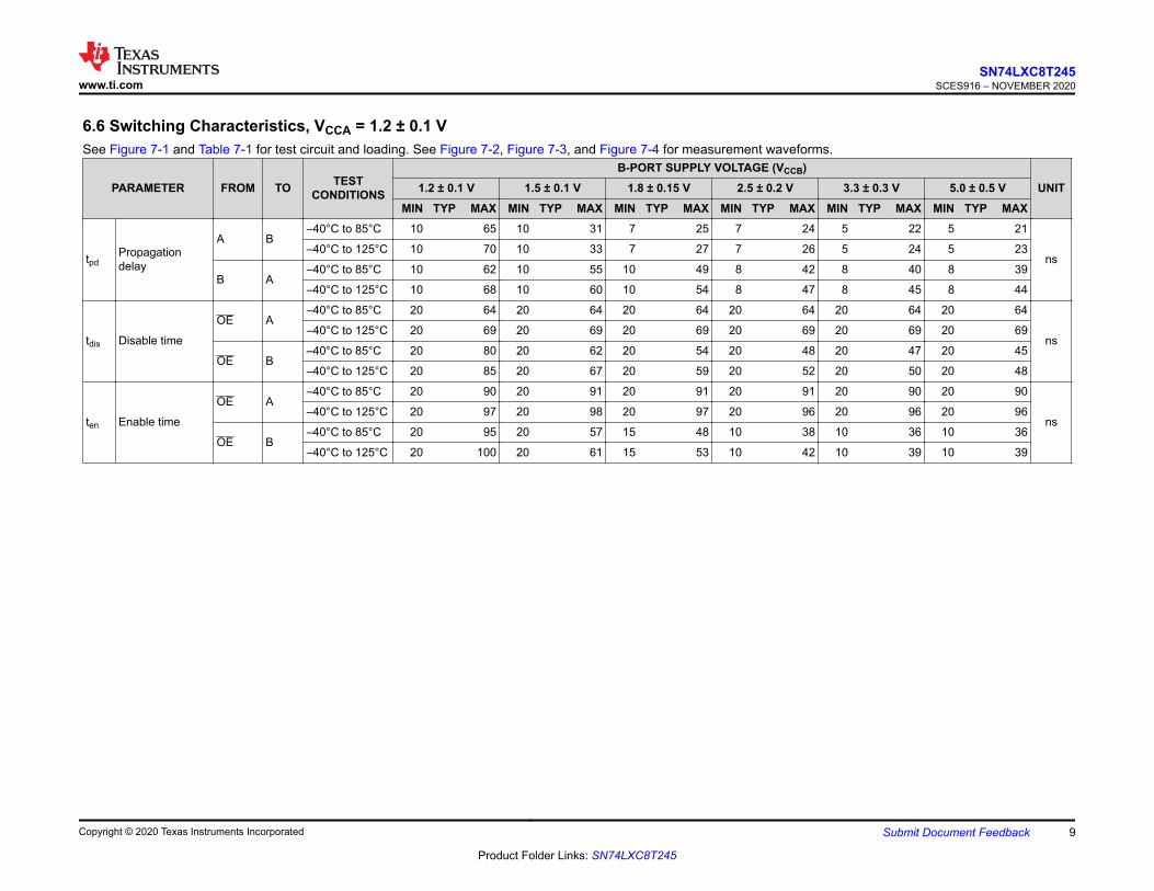
6.6 Switching Characteristics, VCCA = 1.2 ± 0.1 VSee Figure 7-1 and Table 7-1 for test circuit and loading. See Figure 7-2, Figure 7-3, and Figure 7-4 for measurement waveforms.
PARAMETER FROM TO TESTCONDITIONS
B-PORT SUPPLY VOLTAGE (VCCB)UNIT1.2 ± 0.1 V 1.5 ± 0.1 V 1.8 ± 0.15 V 2.5 ± 0.2 V 3.3 ± 0.3 V 5.0 ± 0.5 V
MIN TYP MAX MIN TYP MAX MIN TYP MAX MIN TYP MAX MIN TYP MAX MIN TYP MAX
tpdPropagationdelay
A B–40°C to 85°C 10 65 10 31 7 25 7 24 5 22 5 21
ns–40°C to 125°C 10 70 10 33 7 27 7 26 5 24 5 23
B A–40°C to 85°C 10 62 10 55 10 49 8 42 8 40 8 39
–40°C to 125°C 10 68 10 60 10 54 8 47 8 45 8 44
tdis Disable time
OE A–40°C to 85°C 20 64 20 64 20 64 20 64 20 64 20 64
ns–40°C to 125°C 20 69 20 69 20 69 20 69 20 69 20 69
OE B–40°C to 85°C 20 80 20 62 20 54 20 48 20 47 20 45
–40°C to 125°C 20 85 20 67 20 59 20 52 20 50 20 48
ten Enable time
OE A–40°C to 85°C 20 90 20 91 20 91 20 91 20 90 20 90
ns–40°C to 125°C 20 97 20 98 20 97 20 96 20 96 20 96
OE B–40°C to 85°C 20 95 20 57 15 48 10 38 10 36 10 36
–40°C to 125°C 20 100 20 61 15 53 10 42 10 39 10 39
www.ti.comSN74LXC8T245
SCES916 – NOVEMBER 2020
Copyright © 2020 Texas Instruments Incorporated Submit Document Feedback 9
Product Folder Links: SN74LXC8T245

6.7 Switching Characteristics, VCCA = 1.5 ± 0.1 VSee Figure 7-1 and Table 7-1 for test circuit and loading. See Figure 7-2, Figure 7-3, and Figure 7-4 for measurement waveforms.
PARAMETER FROM TO TESTCONDITIONS
B–PORT SUPPLY VOLTAGE (VCCB)UNIT1.2 ± 0.1 V 1.5 ± 0.1 V 1.8 ± 0.15 V 2.5 ± 0.2 V 3.3 ± 0.3 V 5.0 ± 0.5 V
MIN TYP MAX MIN TYP MAX MIN TYP MAX MIN TYP MAX MIN TYP MAX MIN TYP MAX
tpdPropagationdelay
A B–40°C to 85°C 10 52 5 25 5 23 5 17 5 14 3 13
ns–40°C to 125°C 10 57 5 26 5 23 5 18 5 16 3 14
B A–40°C to 85°C 8 36 7 28 7 26 5 20 5 18 5 17
–40°C to 125°C 8 40 7 29 7 26 5 22 5 20 5 18
tdis Disable time
OE A–40°C to 85°C 15 40 15 40 15 40 15 40 15 40 15 40
ns–40°C to 125°C 15 44 15 44 15 44 15 44 15 44 15 44
OE B–40°C to 85°C 20 69 20 50 15 45 15 35 15 34 14 31
–40°C to 125°C 20 74 20 54 15 48 15 39 15 37 14 33
ten Enable time
OE A–40°C to 85°C 15 48 15 48 15 48 15 48 15 48 15 48
ns–40°C to 125°C 15 52 15 52 15 52 15 52 15 52 15 52
OE B–40°C to 85°C 20 85 15 50 15 40 10 31 10 26 10 24
–40°C to 125°C 20 91 15 54 15 44 10 33 10 29 10 26
SN74LXC8T245SCES916 – NOVEMBER 2020 www.ti.com
10 Submit Document Feedback Copyright © 2020 Texas Instruments Incorporated
Product Folder Links: SN74LXC8T245

6.8 Switching Characteristics, VCCA = 1.8 ± 0.15 VSee Figure 7-1 and Table 7-1 for test circuit and loading. See Figure 7-2, Figure 7-3, and Figure 7-4 for measurement waveforms.
PARAMETER FROM TO TESTCONDITIONS
B–PORT SUPPLY VOLTAGE (VCCB)UNIT1.2 ± 0.1 V 1.5 ± 0.1 V 1.8 ± 0.15 V 2.5 ± 0.2 V 3.3 ± 0.3 V 5.0 ± 0.5 V
MIN TYP MAX MIN TYP MAX MIN TYP MAX MIN TYP MAX MIN TYP MAX MIN TYP MAX
tpdPropagationdelay
A B–40°C to 85°C 8 50 6 21 6 18 4 14 4 11 2 10
ns–40°C to 125°C 8 53 6 23 6 20 4 15 4 12 2 11
B A–40°C to 85°C 5 32 5 21 5 19 4 17 4 15 4 15
–40°C to 125°C 5 33 5 23 5 21 4 18 4 16 4 16
tdis Disable time
OE A–40°C to 85°C 10 34 10 33 10 33 10 33 10 33 10 33
ns–40°C to 125°C 10 36 10 35 10 35 10 35 10 35 10 35
OE B–40°C to 85°C 20 64 15 45 15 40 12 31 12 31 10 26
–40°C to 125°C 20 69 15 49 15 44 12 33 12 38 10 28
ten Enable time
OE A–40°C to 85°C 10 38 10 38 10 38 10 38 10 38 10 38
ns–40°C to 125°C 10 40 10 40 10 40 10 40 10 40 10 40
OE B–40°C to 85°C 20 84 15 47 10 38 10 29 10 25 8 23
–40°C to 125°C 20 89 15 51 10 42 10 30 10 26 8 25
www.ti.comSN74LXC8T245
SCES916 – NOVEMBER 2020
Copyright © 2020 Texas Instruments Incorporated Submit Document Feedback 11
Product Folder Links: SN74LXC8T245
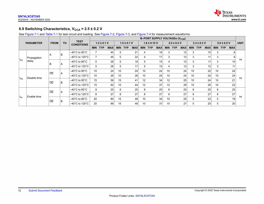
6.9 Switching Characteristics, VCCA = 2.5 ± 0.2 VSee Figure 7-1 and Table 7-1 for test circuit and loading. See Figure 7-2, Figure 7-3, and Figure 7-4 for measurement waveforms.
PARAMETER FROM TO TESTCONDITIONS
B–PORT SUPPLY VOLTAGEe (VCCB)UNIT1.2 ± 0.1 V 1.5 ± 0.1 V 1.8 ± 0.15 V 2.5 ± 0.2 V 3.3 ± 0.3 V 5.0 ± 0.5 V
MIN TYP MAX MIN TYP MAX MIN TYP MAX MIN TYP MAX MIN TYP MAX MIN TYP MAX
tpdPropagationdelay
A B–40°C to 85°C 7 40 5 21 4 16 3 12 3 10 3 8
ns–40°C to 125°C 7 45 5 22 4 17 3 13 3 11 3 9
B A–40°C to 85°C 5 26 5 16 5 15 4 12 3 11 3 10
–40°C to 125°C 5 28 5 17 5 15 4 13 3 12 3 11
tdis Disable time
OE A–40°C to 85°C 10 24 10 24 10 24 10 24 10 22 10 24
ns–40°C to 125°C 10 26 10 26 10 24 10 24 10 24 10 24
OE B–40°C to 85°C 15 56 15 41 12 34 12 25 10 24 10 21
–40°C to 125°C 15 62 15 44 12 37 12 29 10 26 10 22
ten Enable time
OE A–40°C to 85°C 8 25 8 25 8 25 8 25 8 25 8 25
ns–40°C to 125°C 8 27 8 27 8 27 8 27 8 27 8 27
OE B–40°C to 85°C 20 80 15 46 10 34 10 25 5 23 5 18
–40°C to 125°C 20 86 15 48 10 37 10 27 5 25 5 20
SN74LXC8T245SCES916 – NOVEMBER 2020 www.ti.com
12 Submit Document Feedback Copyright © 2020 Texas Instruments Incorporated
Product Folder Links: SN74LXC8T245
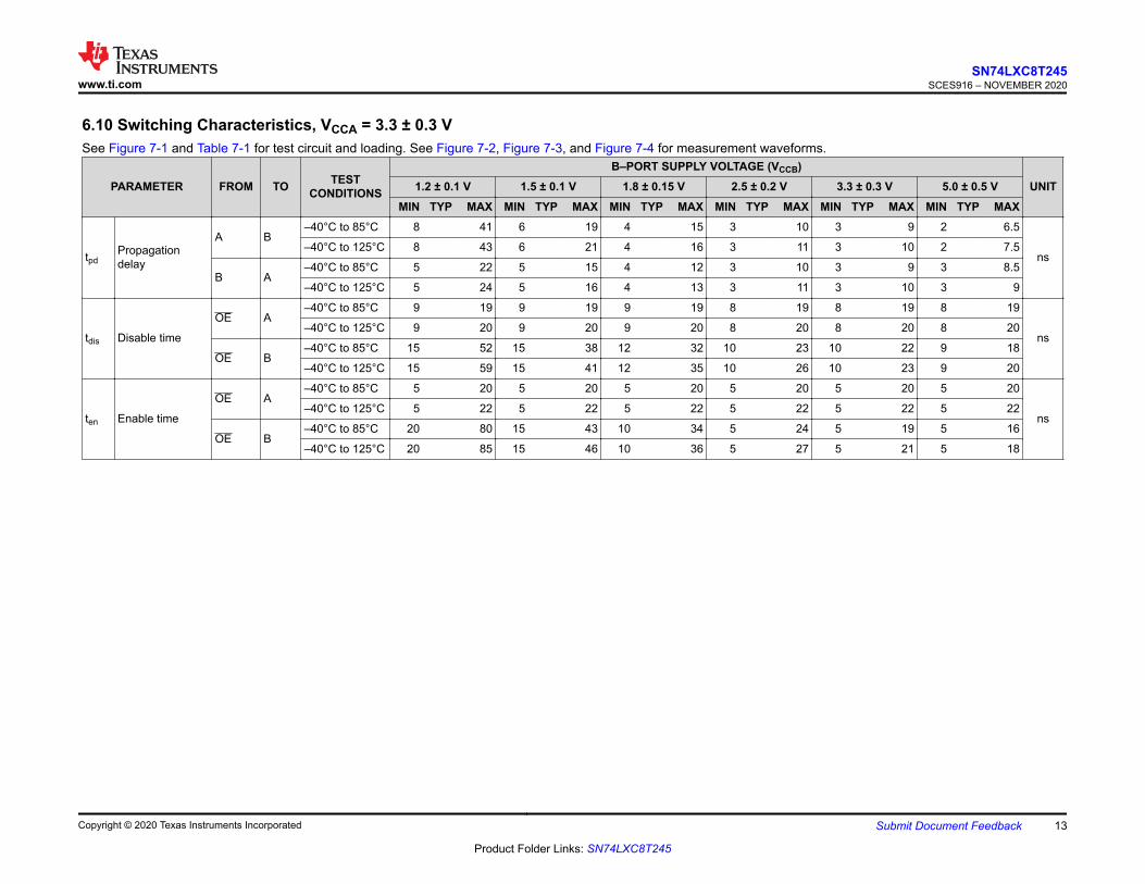
6.10 Switching Characteristics, VCCA = 3.3 ± 0.3 VSee Figure 7-1 and Table 7-1 for test circuit and loading. See Figure 7-2, Figure 7-3, and Figure 7-4 for measurement waveforms.
PARAMETER FROM TO TESTCONDITIONS
B–PORT SUPPLY VOLTAGE (VCCB)UNIT1.2 ± 0.1 V 1.5 ± 0.1 V 1.8 ± 0.15 V 2.5 ± 0.2 V 3.3 ± 0.3 V 5.0 ± 0.5 V
MIN TYP MAX MIN TYP MAX MIN TYP MAX MIN TYP MAX MIN TYP MAX MIN TYP MAX
tpdPropagationdelay
A B–40°C to 85°C 8 41 6 19 4 15 3 10 3 9 2 6.5
ns–40°C to 125°C 8 43 6 21 4 16 3 11 3 10 2 7.5
B A–40°C to 85°C 5 22 5 15 4 12 3 10 3 9 3 8.5
–40°C to 125°C 5 24 5 16 4 13 3 11 3 10 3 9
tdis Disable time
OE A–40°C to 85°C 9 19 9 19 9 19 8 19 8 19 8 19
ns–40°C to 125°C 9 20 9 20 9 20 8 20 8 20 8 20
OE B–40°C to 85°C 15 52 15 38 12 32 10 23 10 22 9 18
–40°C to 125°C 15 59 15 41 12 35 10 26 10 23 9 20
ten Enable time
OE A–40°C to 85°C 5 20 5 20 5 20 5 20 5 20 5 20
ns–40°C to 125°C 5 22 5 22 5 22 5 22 5 22 5 22
OE B–40°C to 85°C 20 80 15 43 10 34 5 24 5 19 5 16
–40°C to 125°C 20 85 15 46 10 36 5 27 5 21 5 18
www.ti.comSN74LXC8T245
SCES916 – NOVEMBER 2020
Copyright © 2020 Texas Instruments Incorporated Submit Document Feedback 13
Product Folder Links: SN74LXC8T245
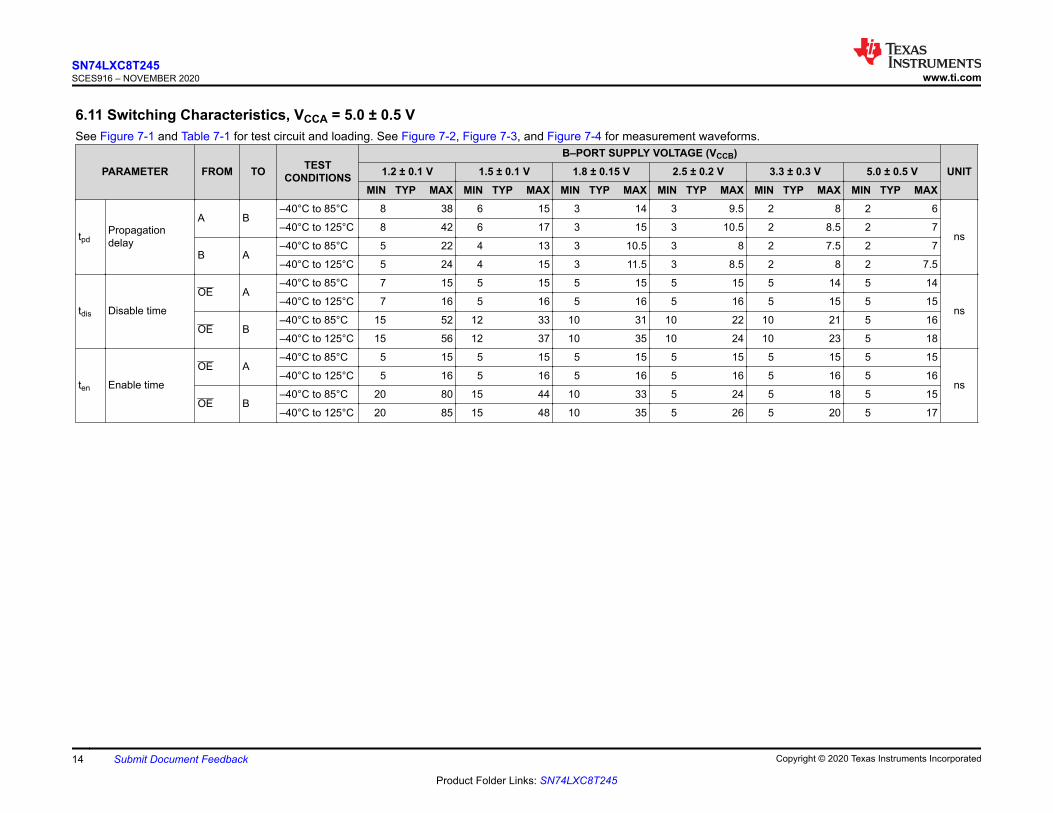
6.11 Switching Characteristics, VCCA = 5.0 ± 0.5 VSee Figure 7-1 and Table 7-1 for test circuit and loading. See Figure 7-2, Figure 7-3, and Figure 7-4 for measurement waveforms.
PARAMETER FROM TO TESTCONDITIONS
B–PORT SUPPLY VOLTAGE (VCCB)UNIT1.2 ± 0.1 V 1.5 ± 0.1 V 1.8 ± 0.15 V 2.5 ± 0.2 V 3.3 ± 0.3 V 5.0 ± 0.5 V
MIN TYP MAX MIN TYP MAX MIN TYP MAX MIN TYP MAX MIN TYP MAX MIN TYP MAX
tpdPropagationdelay
A B–40°C to 85°C 8 38 6 15 3 14 3 9.5 2 8 2 6
ns–40°C to 125°C 8 42 6 17 3 15 3 10.5 2 8.5 2 7
B A–40°C to 85°C 5 22 4 13 3 10.5 3 8 2 7.5 2 7
–40°C to 125°C 5 24 4 15 3 11.5 3 8.5 2 8 2 7.5
tdis Disable time
OE A–40°C to 85°C 7 15 5 15 5 15 5 15 5 14 5 14
ns–40°C to 125°C 7 16 5 16 5 16 5 16 5 15 5 15
OE B–40°C to 85°C 15 52 12 33 10 31 10 22 10 21 5 16
–40°C to 125°C 15 56 12 37 10 35 10 24 10 23 5 18
ten Enable time
OE A–40°C to 85°C 5 15 5 15 5 15 5 15 5 15 5 15
ns–40°C to 125°C 5 16 5 16 5 16 5 16 5 16 5 16
OE B–40°C to 85°C 20 80 15 44 10 33 5 24 5 18 5 15
–40°C to 125°C 20 85 15 48 10 35 5 26 5 20 5 17
SN74LXC8T245SCES916 – NOVEMBER 2020 www.ti.com
14 Submit Document Feedback Copyright © 2020 Texas Instruments Incorporated
Product Folder Links: SN74LXC8T245
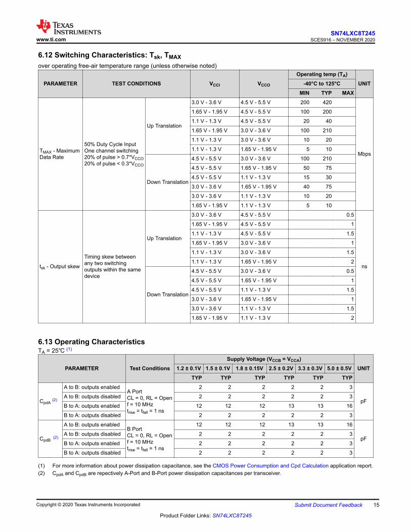
6.12 Switching Characteristics: Tsk, TMAXover operating free-air temperature range (unless otherwise noted)
PARAMETER TEST CONDITIONS VCCI VCCO
Operating temp (TA)UNIT-40°C to 125°C
MIN TYP MAX
TMAX - MaximumData Rate
50% Duty Cycle InputOne channel switching20% of pulse > 0.7*VCCO20% of pulse < 0.3*VCCO
Up Translation
3.0 V - 3.6 V 4.5 V - 5.5 V 200 420
Mbps
1.65 V - 1.95 V 4.5 V - 5.5 V 100 200
1.1 V - 1.3 V 4.5 V - 5.5 V 20 40
1.65 V - 1.95 V 3.0 V - 3.6 V 100 210
1.1 V - 1.3 V 3.0 V - 3.6 V 10 20
1.1 V - 1.3 V 1.65 V - 1.95 V 5 10
Down Translation
4.5 V - 5.5 V 3.0 V - 3.6 V 100 210
4.5 V - 5.5 V 1.65 V - 1.95 V 50 75
4.5 V - 5.5 V 1.1 V - 1.3 V 15 30
3.0 V - 3.6 V 1.65 V - 1.95 V 40 75
3.0 V - 3.6 V 1.1 V - 1.3 V 10 20
1.65 V - 1.95 V 1.1 V - 1.3 V 5 10
tsk - Output skew
Timing skew betweenany two switchingoutputs within the samedevice
Up Translation
3.0 V - 3.6 V 4.5 V - 5.5 V 0.5
ns
1.65 V - 1.95 V 4.5 V - 5.5 V 1
1.1 V - 1.3 V 4.5 V - 5.5 V 1.5
1.65 V - 1.95 V 3.0 V - 3.6 V 1
1.1 V - 1.3 V 3.0 V - 3.6 V 1.5
1.1 V - 1.3 V 1.65 V - 1.95 V 2
Down Translation
4.5 V - 5.5 V 3.0 V - 3.6 V 0.5
4.5 V - 5.5 V 1.65 V - 1.95 V 1
4.5 V - 5.5 V 1.1 V - 1.3 V 1.5
3.0 V - 3.6 V 1.65 V - 1.95 V 1
3.0 V - 3.6 V 1.1 V - 1.3 V 1.5
1.65 V - 1.95 V 1.1 V - 1.3 V 2
6.13 Operating CharacteristicsTA = 25℃ (1)
PARAMETER Test ConditionsSupply Voltage (VCCB = VCCA)
UNIT1.2 ± 0.1V 1.5 ± 0.1V 1.8 ± 0.15V 2.5 ± 0.2V 3.3 ± 0.3V 5.0 ± 0.5VTYP TYP TYP TYP TYP TYP
CpdA (2)
A to B: outputs enabledA PortCL = 0, RL = Openf = 10 MHztrise = tfall = 1 ns
2 2 2 2 2 3
pFA to B: outputs disabled 2 2 2 2 2 3
B to A: outputs enabled 12 12 12 13 13 16
B to A: outputs disabled 2 2 2 2 2 3
CpdB (2)
A to B: outputs enabledB PortCL = 0, RL = Openf = 10 MHztrise = tfall = 1 ns
12 12 12 13 13 16
pFA to B: outputs disabled 2 2 2 2 2 3
B to A: outputs enabled 2 2 2 2 2 3
B to A: outputs disabled 2 2 2 2 2 3
(1) For more information about power dissipation capacitance, see the CMOS Power Consumption and Cpd Calculation application report.(2) CpdA and CpdB are repectively A-Port and B-Port power dissipation capacitances per transceiver.
www.ti.comSN74LXC8T245
SCES916 – NOVEMBER 2020
Copyright © 2020 Texas Instruments Incorporated Submit Document Feedback 15
Product Folder Links: SN74LXC8T245
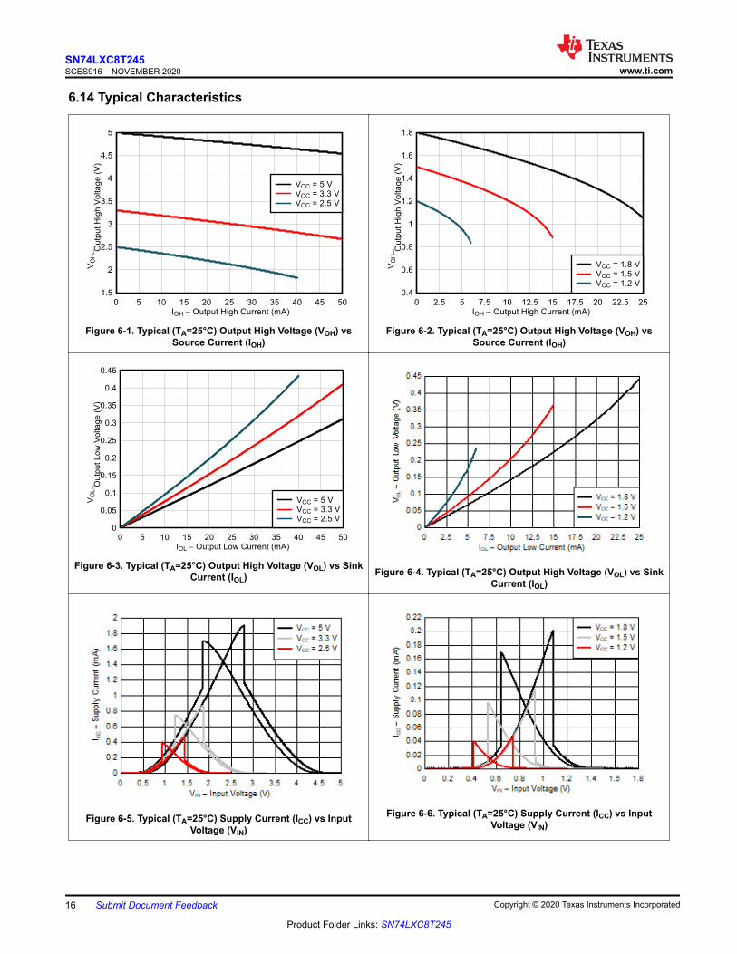
6.14 Typical Characteristics
IOH Output High Current (mA)
V OH O
utpu
t Hig
h Vo
ltage
(V)
0 5 10 15 20 25 30 35 40 45 501.5
2
2.5
3
3.5
4
4.5
5
VCC = 5 VVCC = 3.3 VVCC = 2.5 V
Figure 6-1. Typical (TA=25°C) Output High Voltage (VOH) vsSource Current (IOH)
IOH Output High Current (mA)
V OH O
utpu
t Hig
h Vo
ltage
(V)
0 2.5 5 7.5 10 12.5 15 17.5 20 22.5 250.4
0.6
0.8
1
1.2
1.4
1.6
1.8
VCC = 1.8 VVCC = 1.5 VVCC = 1.2 V
Figure 6-2. Typical (TA=25°C) Output High Voltage (VOH) vsSource Current (IOH)
IOL Output Low Current (mA)
V OL O
utpu
t Low
Vol
tage
(V)
0 5 10 15 20 25 30 35 40 45 500
0.05
0.1
0.15
0.2
0.25
0.3
0.35
0.4
0.45
VCC = 5 VVCC = 3.3 VVCC = 2.5 V
Figure 6-3. Typical (TA=25°C) Output High Voltage (VOL) vs SinkCurrent (IOL) Figure 6-4. Typical (TA=25°C) Output High Voltage (VOL) vs Sink
Current (IOL)
Figure 6-5. Typical (TA=25°C) Supply Current (ICC) vs InputVoltage (VIN)
Figure 6-6. Typical (TA=25°C) Supply Current (ICC) vs InputVoltage (VIN)
SN74LXC8T245SCES916 – NOVEMBER 2020 www.ti.com
16 Submit Document Feedback Copyright © 2020 Texas Instruments Incorporated
Product Folder Links: SN74LXC8T245
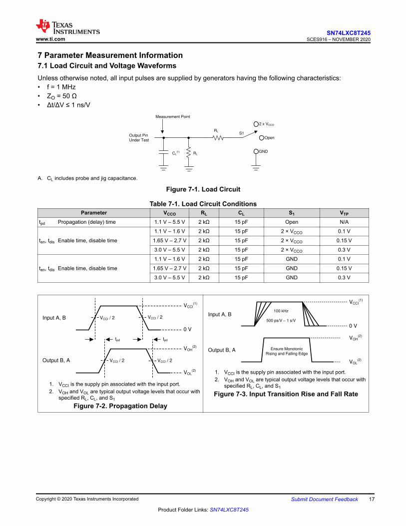
7 Parameter Measurement Information7.1 Load Circuit and Voltage WaveformsUnless otherwise noted, all input pulses are supplied by generators having the following characteristics:• f = 1 MHz• ZO = 50 Ω• Δt/ΔV ≤ 1 ns/V
Output Pin
Under Test
CL(1) RL
RLS1
GND
Open
2 x VCCO
Measurement Point
A. CL includes probe and jig capacitance.
Figure 7-1. Load Circuit
Table 7-1. Load Circuit ConditionsParameter VCCO RL CL S1 VTP
tpd Propagation (delay) time 1.1 V – 5.5 V 2 kΩ 15 pF Open N/A
ten, tdis Enable time, disable time
1.1 V – 1.6 V 2 kΩ 15 pF 2 × VCCO 0.1 V
1.65 V – 2.7 V 2 kΩ 15 pF 2 × VCCO 0.15 V
3.0 V – 5.5 V 2 kΩ 15 pF 2 × VCCO 0.3 V
ten, tdis Enable time, disable time
1.1 V – 1.6 V 2 kΩ 15 pF GND 0.1 V
1.65 V – 2.7 V 2 kΩ 15 pF GND 0.15 V
3.0 V – 5.5 V 2 kΩ 15 pF GND 0.3 V
Input A, B
VCCI(1)
VCCI / 2
0 V
Output B, A
VOH(2)
VOL(2)
tpd tpd
VCCI / 2
VCCI / 2 VCCI / 2
1. VCCI is the supply pin associated with the input port.2. VOH and VOL are typical output voltage levels that occur with
specified RL, CL, and S1
Figure 7-2. Propagation Delay
VCCI(1)
0 V
100 kHz
500 ps/V ± 1 s/V
VOH(2)
VOL(2)
Ensure Monotonic
Rising and Falling EdgeOutput B, A
Input A, B
1. VCCI is the supply pin associated with the input port.2. VOH and VOL are typical output voltage levels that occur with
specified RL, CL, and S1
Figure 7-3. Input Transition Rise and Fall Rate
www.ti.comSN74LXC8T245
SCES916 – NOVEMBER 2020
Copyright © 2020 Texas Instruments Incorporated Submit Document Feedback 17
Product Folder Links: SN74LXC8T245

VCCA
VCCA / 2
Output(1)
tdis
GND
VCCA / 2
VCCO(3)
VOL(4)
VOL + VTP
ten
VCCO / 2
Output(2)
VOH(4)
GND
VOH - VTP
VCCO / 2
OE
A. Output waveform on the condition that input is driven to a valid Logic Low.B. Output waveform on the condition that input is driven to a valid Logic High.C. VCCO is the supply pin associated with the output port.D. VOH and VOL are typical output voltage levels with specified RL, CL, and S1.
Figure 7-4. Enable Time And Disable Time
SN74LXC8T245SCES916 – NOVEMBER 2020 www.ti.com
18 Submit Document Feedback Copyright © 2020 Texas Instruments Incorporated
Product Folder Links: SN74LXC8T245
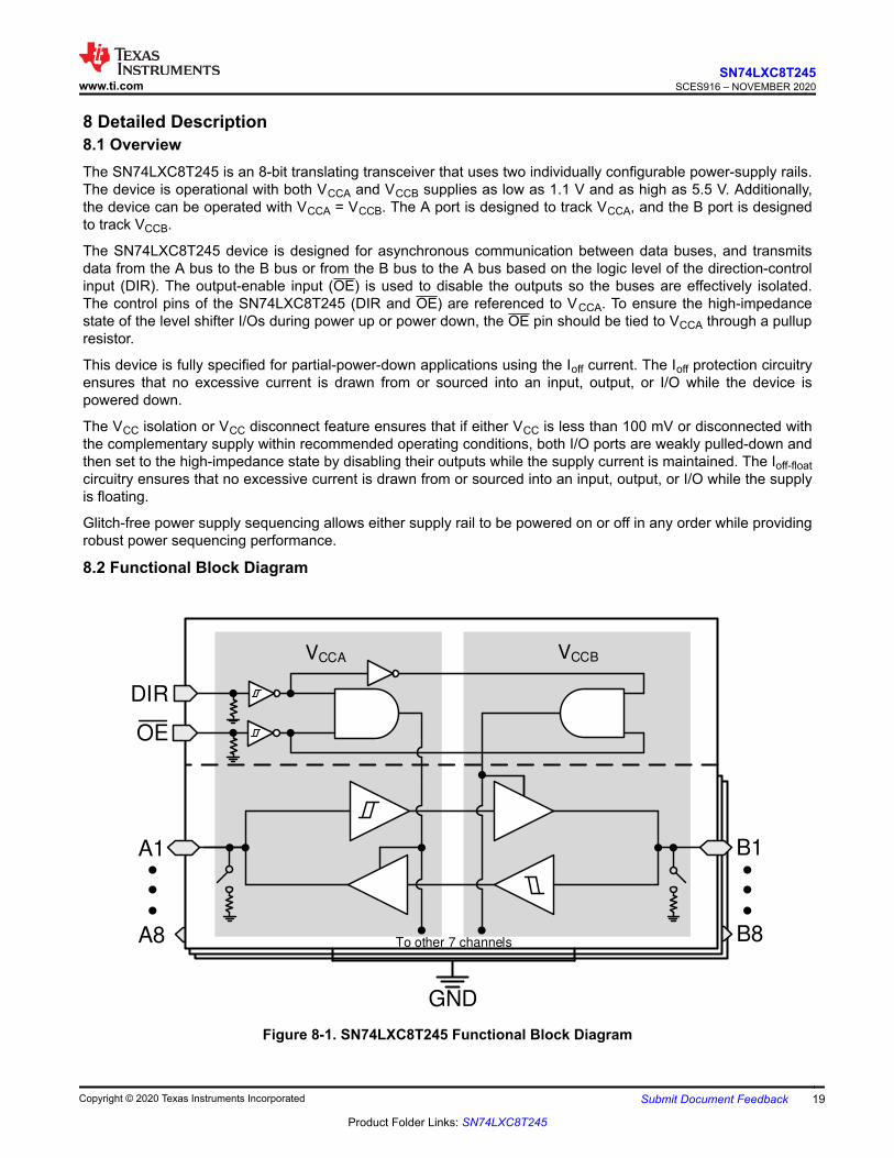
8 Detailed Description8.1 OverviewThe SN74LXC8T245 is an 8-bit translating transceiver that uses two individually configurable power-supply rails.The device is operational with both VCCA and VCCB supplies as low as 1.1 V and as high as 5.5 V. Additionally,the device can be operated with VCCA = VCCB. The A port is designed to track VCCA, and the B port is designedto track VCCB.
The SN74LXC8T245 device is designed for asynchronous communication between data buses, and transmitsdata from the A bus to the B bus or from the B bus to the A bus based on the logic level of the direction-controlinput (DIR). The output-enable input (OE) is used to disable the outputs so the buses are effectively isolated.The control pins of the SN74LXC8T245 (DIR and OE) are referenced to VCCA. To ensure the high-impedancestate of the level shifter I/Os during power up or power down, the OE pin should be tied to VCCA through a pullupresistor.
This device is fully specified for partial-power-down applications using the Ioff current. The Ioff protection circuitryensures that no excessive current is drawn from or sourced into an input, output, or I/O while the device ispowered down.
The VCC isolation or VCC disconnect feature ensures that if either VCC is less than 100 mV or disconnected withthe complementary supply within recommended operating conditions, both I/O ports are weakly pulled-down andthen set to the high-impedance state by disabling their outputs while the supply current is maintained. The Ioff-floatcircuitry ensures that no excessive current is drawn from or sourced into an input, output, or I/O while the supplyis floating.
Glitch-free power supply sequencing allows either supply rail to be powered on or off in any order while providingrobust power sequencing performance.
8.2 Functional Block Diagram
A8 B8
A1 B1
OE
DIR
VCCA VCCB
To other 7 channels
GND
Figure 8-1. SN74LXC8T245 Functional Block Diagram
www.ti.comSN74LXC8T245
SCES916 – NOVEMBER 2020
Copyright © 2020 Texas Instruments Incorporated Submit Document Feedback 19
Product Folder Links: SN74LXC8T245
8.3 Feature Description8.3.1 CMOS Schmitt-Trigger Inputs with Integrated Pulldowns
Standard CMOS inputs are high impedance and are typically modeled as a resistor in parallel with the inputcapacitance given in the Electrical Characteristics. The worst case resistance is calculated with the maximuminput voltage, given in the Absolute Maximum Ratings, and the maximum input leakage current, given in theElectrical Characteristics, using ohm's law (R = V ÷ I).
The Schmitt-trigger input architecture provides hysteresis as defined by ΔV T in the Electrical Characteristics,which makes this device extremely tolerant to slow or noisy inputs. Driving the inputs slowly will increasedynamic current consumption of the device. For additional information regarding Schmitt-trigger inputs, seeUnderstanding Schmitt Triggers.
8.3.1.1 I/O's with Integrated Dynamic Pull-Down Resistors
Input circuits of the data I/O's are always active even when the device is disabled. It is recommended to keep avalid voltage level at the I/O's to avoid high current consumption. To help avoid floating inputs on the I/O's duringdisabling, this device has 100-kΩ typical integrated weak dynamic pull-downs on all data I/O's. When the deviceis disabled, the dynamic pull-downs are activated for only a short period of time to help drive and keep low anyfloating inputs before the device I/O's become high impedance. If the I/O lines are to be floated after the deviceis disabled, it is recommended to keep them at a valid input voltage level using external pull-downs. This featureis ideal for loads of 30 pF or less. If greater capactive loading is present then external pull-downs arerecommended. If an external pull-up is required, it should be no larger than 15 kΩ to avoid contention with the100 kΩ internal pull-down.
8.3.1.2 Control Inputs with Integrated Static Pull-Down Resistors
Similar to the data I/O's, floating control inputs can cause high current consumption. To help avoid this concern,this device has integrated weak static pull-downs of 5-MΩ typical on the control inputs (DIR and OE). These pull-downs are always present so for example if the DIR pin is left floating, then the B port will be configured as aninput and the A port configured as an output.
8.3.2 Balanced High-Drive CMOS Push-Pull Outputs
A balanced output allows the device to sink and source similar currents. The high drive capability of this devicecreates fast edges into light loads so routing and load conditions should be considered to prevent ringing.Additionally, the outputs of this device are capable of driving larger currents than the device can sustain withoutbeing damaged. The electrical and thermal limits defined in the Absolute Maximum Ratings must be followed atall times.
8.3.3 Partial Power Down (Ioff)
The inputs and outputs for this device enter a high-impedance state when the device is powered down, inhibitingcurrent backflow into the device. The maximum leakage into or out of any input or output pin on the device isspecified by Ioff in the Electrical Characteristics.
SN74LXC8T245SCES916 – NOVEMBER 2020 www.ti.com
20 Submit Document Feedback Copyright © 2020 Texas Instruments Incorporated
Product Folder Links: SN74LXC8T245

8.3.4 VCC Isolation and VCC Disconnect (Ioff-float)
This device has I/O's with Integrated Dynamic Pull-Down Resistors. The I/O's will get pulled down and then entera high-impedance state when either supply is < 100 mV or left floating (disconnected), while the other supply isstill connected to the device. It is recommended that the I/O's for this device are not driven and kept at a logiclow state prior to floating (disconnecting) either supply.
The maximum supply current is specified by I CCx, while V CCx is floating, in the Electrical Characterstics. Themaximum leakage into or out of any input or output pin on the device is specified by I off(float) in the ElectricalCharacteristics.
Hi-Z Hi-ZA1 B1
OE
VCCBVCCA
DIR
VCCA VCCB
GND
Supply disconnected ICCB maintained
Disabled
Disabled
Ioff(float)Ioff(float)
Figure 8-2. VCC Disconnect Feature
8.3.5 Over-voltage Tolerant Inputs
Input signals to this device can be driven above the supply voltage so long as they remain below the maximuminput voltage value specified in the Recommended Operating Conditions.
8.3.6 Glitch-free Power Supply Sequencing
Either supply rail may be powered on or off in any order without producing a glitch on the I/Os (that is, where theoutput erroneously transitions to VCC when it should be held low or vice versa). Glitches of this nature can bemisinterpreted by a peripheral as a valid data bit, which could trigger a false device reset of the peripheral, afalse device configuration of the peripheral, or even a false data initialization by the peripheral.
www.ti.comSN74LXC8T245
SCES916 – NOVEMBER 2020
Copyright © 2020 Texas Instruments Incorporated Submit Document Feedback 21
Product Folder Links: SN74LXC8T245
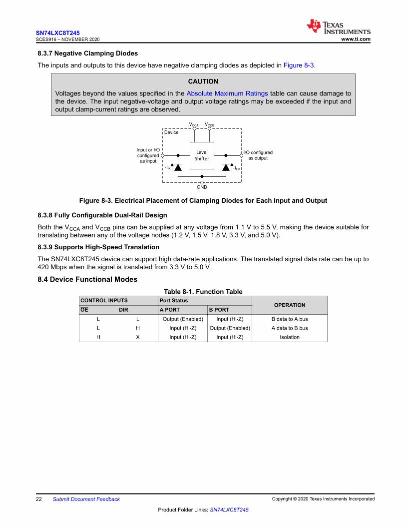
8.3.7 Negative Clamping Diodes
The inputs and outputs to this device have negative clamping diodes as depicted in Figure 8-3.
CAUTION
Voltages beyond the values specified in the Absolute Maximum Ratings table can cause damage tothe device. The input negative-voltage and output voltage ratings may be exceeded if the input andoutput clamp-current ratings are observed.
GND
Level
Shifter
Input or I/O
configured
as input
VCCA
Device
-IIK -IOK
VCCB
I/O configured
as output
Figure 8-3. Electrical Placement of Clamping Diodes for Each Input and Output
8.3.8 Fully Configurable Dual-Rail Design
Both the VCCA and VCCB pins can be supplied at any voltage from 1.1 V to 5.5 V, making the device suitable fortranslating between any of the voltage nodes (1.2 V, 1.5 V, 1.8 V, 3.3 V, and 5.0 V).
8.3.9 Supports High-Speed Translation
The SN74LXC8T245 device can support high data-rate applications. The translated signal data rate can be up to420 Mbps when the signal is translated from 3.3 V to 5.0 V.
8.4 Device Functional ModesTable 8-1. Function Table
CONTROL INPUTS Port StatusOPERATION
OE DIR A PORT B PORTL L Output (Enabled) Input (Hi-Z) B data to A busL H Input (Hi-Z) Output (Enabled) A data to B busH X Input (Hi-Z) Input (Hi-Z) Isolation
SN74LXC8T245SCES916 – NOVEMBER 2020 www.ti.com
22 Submit Document Feedback Copyright © 2020 Texas Instruments Incorporated
Product Folder Links: SN74LXC8T245
9 Application and ImplementationNote
Information in the following applications sections is not part of the TI component specification, and TIdoes not warrant its accuracy or completeness. TI’s customers are responsible for determiningsuitability of components for their purposes. Customers should validate and test their designimplementation to confirm system functionality.
9.1 Application InformationThe SN74LXC8T245 device can be used in level-translation applications for interfacing devices or systemsoperating at different interface voltages with one another. The SN74LXC8T245 device is ideal for use inapplications where a push-pull driver is connected to the data I/Os. The max data rate can be up to 420 Mbpswhen device translates a signal from 3.3 V to 5.0 V.
9.2 Typical Application
LED Array,
FET Array,
Buzzer,
MCU,
Etc...
Controller
VCCA
GPIO7 PWM7
GPIO1 PWM1
GPIO0 PWM0
1010
VCCB
SN74LXC8T245
Figure 9-1. LED Driver Application
9.2.1 Design Requirements
For this design example, use the parameters listed in Table 9-1.
Table 9-1. Design ParametersDESIGN PARAMETERS EXAMPLE VALUES
Input voltage range 1.1 V to 5.5 V
Output voltage range 1.1 V to 5.5 V
9.2.2 Detailed Design Procedure
To begin the design process, determine the following:• Input voltage range
– Use the supply voltage of the device that is driving the SN74LXC8T245 device to determine the inputvoltage range. For a valid logic-high, the value must exceed the positive-going input-threshold voltage(Vt+) of the input port. For a valid logic low the value must be less than the negative-going input-thresholdvoltage (Vt-) of the input port.
• Output voltage range– Use the supply voltage of the device that the SN74LXC8T245 device is driving to determine the output
voltage range.
www.ti.comSN74LXC8T245
SCES916 – NOVEMBER 2020
Copyright © 2020 Texas Instruments Incorporated Submit Document Feedback 23
Product Folder Links: SN74LXC8T245
10 Power Supply RecommendationsAlways apply a ground reference to the GND pins first. This device is designed for glitch free power sequencingwithout any supply sequencing requirements such as ramp order or ramp rate.
This device was designed with various power supply sequencing methods in mind to help prevent unintendedtriggering of downstream devices, as described in Glitch-free Power Supply Sequencing.
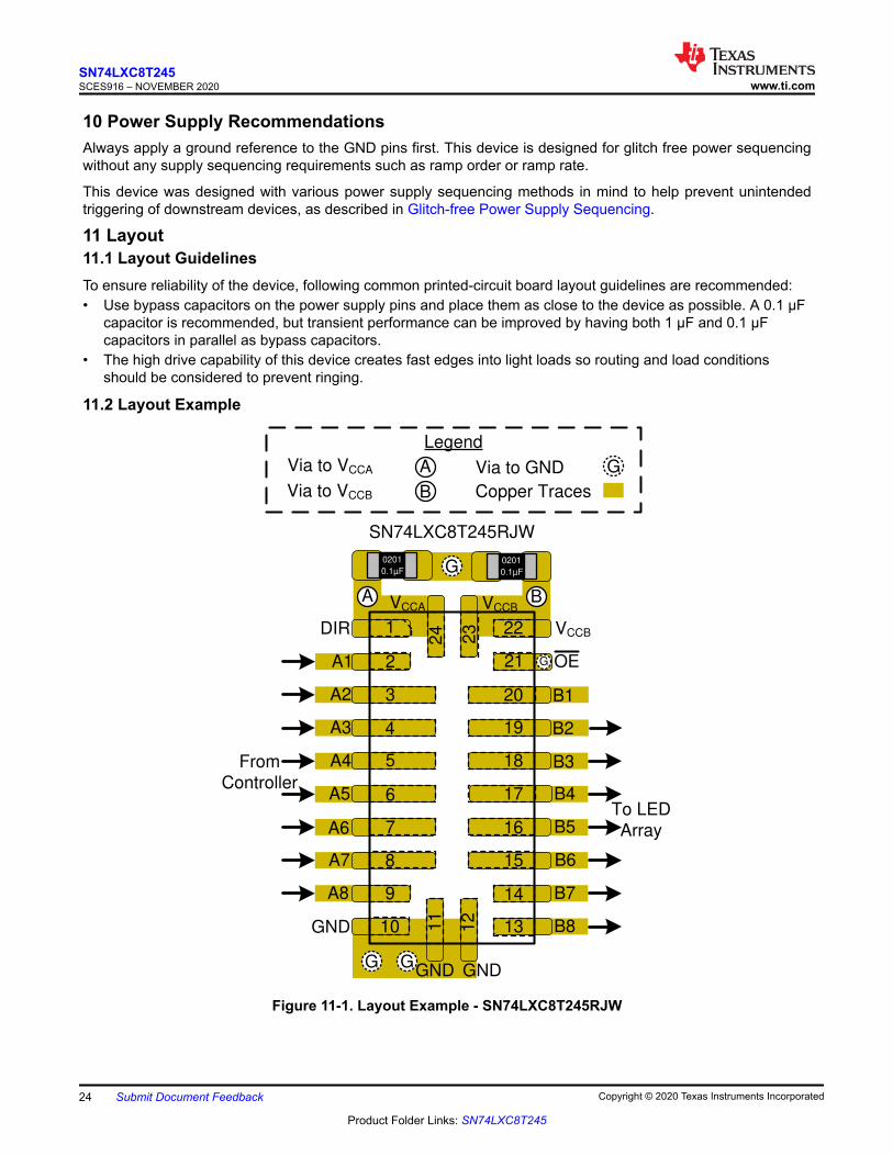
11 Layout11.1 Layout GuidelinesTo ensure reliability of the device, following common printed-circuit board layout guidelines are recommended:• Use bypass capacitors on the power supply pins and place them as close to the device as possible. A 0.1 µF
capacitor is recommended, but transient performance can be improved by having both 1 µF and 0.1 µFcapacitors in parallel as bypass capacitors.
• The high drive capability of this device creates fast edges into light loads so routing and load conditionsshould be considered to prevent ringing.
11.2 Layout Example
241
2
3
4
23
5
6
7
8
9
10 11
12
13
14
15
16
17
18
19
20
21
22 VCCB
B1
B2
B3
B4
B5
B6
B7
B8
OE
VCCA VCCB
GND GND
DIR
A1
A2
A3
A4
A5
A6
A7
A8
GND
Copper TracesVia to VCCB
Via to VCCA Via to GNDA
B
G
Legend
G G
0.1µF
0201
0.1µF
0201
G
A B
G
From Controller
To LEDArray
SN74LXC8T245RJW
Figure 11-1. Layout Example - SN74LXC8T245RJW
SN74LXC8T245SCES916 – NOVEMBER 2020 www.ti.com
24 Submit Document Feedback Copyright © 2020 Texas Instruments Incorporated
Product Folder Links: SN74LXC8T245
12 Device and Documentation Support12.1 Device Support
12.1.1 Regulatory Requirements
No statutory or regulatory requirements apply to this device.
There are no special characteristics for this product.
12.2 Receiving Notification of Documentation UpdatesTo receive notification of documentation updates, navigate to the device product folder on ti.com. Click onSubscribe to updates to register and receive a weekly digest of any product information that has changed. Forchange details, review the revision history included in any revised document.
12.3 Support ResourcesTI E2E™ support forums are an engineer's go-to source for fast, verified answers and design help — straightfrom the experts. Search existing answers or ask your own question to get the quick design help you need.
Linked content is provided "AS IS" by the respective contributors. They do not constitute TI specifications and donot necessarily reflect TI's views; see TI's Terms of Use.
12.4 TrademarksTI E2E™ is a trademark of Texas Instruments.All trademarks are the property of their respective owners.12.5 Electrostatic Discharge Caution
This integrated circuit can be damaged by ESD. Texas Instruments recommends that all integrated circuits be handledwith appropriate precautions. Failure to observe proper handling and installation procedures can cause damage.ESD damage can range from subtle performance degradation to complete device failure. Precision integrated circuits maybe more susceptible to damage because very small parametric changes could cause the device not to meet its publishedspecifications.
12.6 GlossaryTI Glossary This glossary lists and explains terms, acronyms, and definitions.
www.ti.comSN74LXC8T245
SCES916 – NOVEMBER 2020
Copyright © 2020 Texas Instruments Incorporated Submit Document Feedback 25
Product Folder Links: SN74LXC8T245
13 Mechanical, Packaging, and Orderable InformationThe following pages include mechanical, packaging, and orderable information. This information is the mostcurrent data available for the designated devices. This data is subject to change without notice and revision ofthis document. For browser-based versions of this data sheet, refer to the left-hand navigation.
SN74LXC8T245SCES916 – NOVEMBER 2020 www.ti.com
26 Submit Document Feedback Copyright © 2020 Texas Instruments Incorporated
Product Folder Links: SN74LXC8T245
PACKAGE OPTION ADDENDUM
www.ti.com 11-Dec-2020
Addendum-Page 1
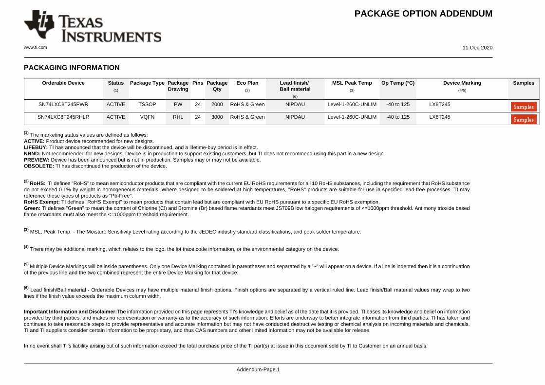
PACKAGING INFORMATION
Orderable Device Status(1)
Package Type PackageDrawing
Pins PackageQty
Eco Plan(2)
Lead finish/Ball material
(6)
MSL Peak Temp(3)
Op Temp (°C) Device Marking(4/5)
Samples
SN74LXC8T245PWR ACTIVE TSSOP PW 24 2000 RoHS & Green NIPDAU Level-1-260C-UNLIM -40 to 125 LX8T245
SN74LXC8T245RHLR ACTIVE VQFN RHL 24 3000 RoHS & Green NIPDAU Level-1-260C-UNLIM -40 to 125 LX8T245
(1) The marketing status values are defined as follows:ACTIVE: Product device recommended for new designs.LIFEBUY: TI has announced that the device will be discontinued, and a lifetime-buy period is in effect.NRND: Not recommended for new designs. Device is in production to support existing customers, but TI does not recommend using this part in a new design.PREVIEW: Device has been announced but is not in production. Samples may or may not be available.OBSOLETE: TI has discontinued the production of the device.
(2) RoHS: TI defines "RoHS" to mean semiconductor products that are compliant with the current EU RoHS requirements for all 10 RoHS substances, including the requirement that RoHS substancedo not exceed 0.1% by weight in homogeneous materials. Where designed to be soldered at high temperatures, "RoHS" products are suitable for use in specified lead-free processes. TI mayreference these types of products as "Pb-Free".RoHS Exempt: TI defines "RoHS Exempt" to mean products that contain lead but are compliant with EU RoHS pursuant to a specific EU RoHS exemption.Green: TI defines "Green" to mean the content of Chlorine (Cl) and Bromine (Br) based flame retardants meet JS709B low halogen requirements of <=1000ppm threshold. Antimony trioxide basedflame retardants must also meet the <=1000ppm threshold requirement.
(3) MSL, Peak Temp. - The Moisture Sensitivity Level rating according to the JEDEC industry standard classifications, and peak solder temperature.
(4) There may be additional marking, which relates to the logo, the lot trace code information, or the environmental category on the device.
(5) Multiple Device Markings will be inside parentheses. Only one Device Marking contained in parentheses and separated by a "~" will appear on a device. If a line is indented then it is a continuationof the previous line and the two combined represent the entire Device Marking for that device.
(6) Lead finish/Ball material - Orderable Devices may have multiple material finish options. Finish options are separated by a vertical ruled line. Lead finish/Ball material values may wrap to twolines if the finish value exceeds the maximum column width.
Important Information and Disclaimer:The information provided on this page represents TI's knowledge and belief as of the date that it is provided. TI bases its knowledge and belief on informationprovided by third parties, and makes no representation or warranty as to the accuracy of such information. Efforts are underway to better integrate information from third parties. TI has taken andcontinues to take reasonable steps to provide representative and accurate information but may not have conducted destructive testing or chemical analysis on incoming materials and chemicals.TI and TI suppliers consider certain information to be proprietary, and thus CAS numbers and other limited information may not be available for release.
In no event shall TI's liability arising out of such information exceed the total purchase price of the TI part(s) at issue in this document sold by TI to Customer on an annual basis.
PACKAGE OPTION ADDENDUM
www.ti.com 11-Dec-2020
Addendum-Page 2
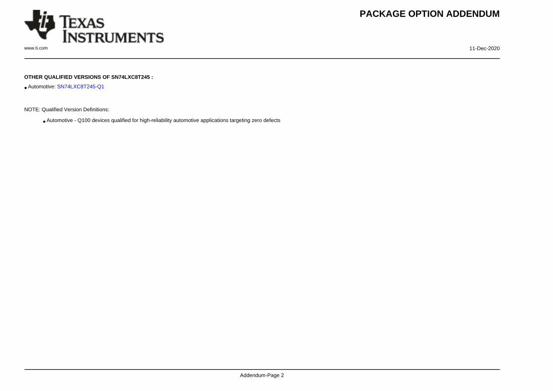
OTHER QUALIFIED VERSIONS OF SN74LXC8T245 :
• Automotive: SN74LXC8T245-Q1
NOTE: Qualified Version Definitions:
• Automotive - Q100 devices qualified for high-reliability automotive applications targeting zero defects

www.ti.com
PACKAGE OUTLINE
C
22X 0.65
2X7.15
24X 0.300.19
TYP6.66.2
1.2 MAX
0.150.05
0.25GAGE PLANE
-80
BNOTE 4
4.54.3
A
NOTE 3
7.97.7
0.750.50
(0.15) TYP
TSSOP - 1.2 mm max heightPW0024ASMALL OUTLINE PACKAGE
4220208/A 02/2017
1
1213
24
0.1 C A B
PIN 1 INDEX AREA
SEE DETAIL A
0.1 C
NOTES: 1. All linear dimensions are in millimeters. Any dimensions in parenthesis are for reference only. Dimensioning and tolerancing per ASME Y14.5M. 2. This drawing is subject to change without notice. 3. This dimension does not include mold flash, protrusions, or gate burrs. Mold flash, protrusions, or gate burrs shall not exceed 0.15 mm per side. 4. This dimension does not include interlead flash. Interlead flash shall not exceed 0.25 mm per side.5. Reference JEDEC registration MO-153.
SEATINGPLANE
A 20DETAIL ATYPICAL
SCALE 2.000

www.ti.com
EXAMPLE BOARD LAYOUT
0.05 MAXALL AROUND
0.05 MINALL AROUND
24X (1.5)
24X (0.45)
22X (0.65)
(5.8)
(R0.05) TYP
TSSOP - 1.2 mm max heightPW0024ASMALL OUTLINE PACKAGE
4220208/A 02/2017
NOTES: (continued) 6. Publication IPC-7351 may have alternate designs. 7. Solder mask tolerances between and around signal pads can vary based on board fabrication site.
LAND PATTERN EXAMPLEEXPOSED METAL SHOWN
SCALE: 10X
SYMM
SYMM
1
12 13
24
15.000
METALSOLDER MASKOPENING
METAL UNDERSOLDER MASK
SOLDER MASKOPENING
EXPOSED METALEXPOSED METAL
SOLDER MASK DETAILS
NON-SOLDER MASKDEFINED
(PREFERRED)
SOLDER MASKDEFINED
www.ti.com
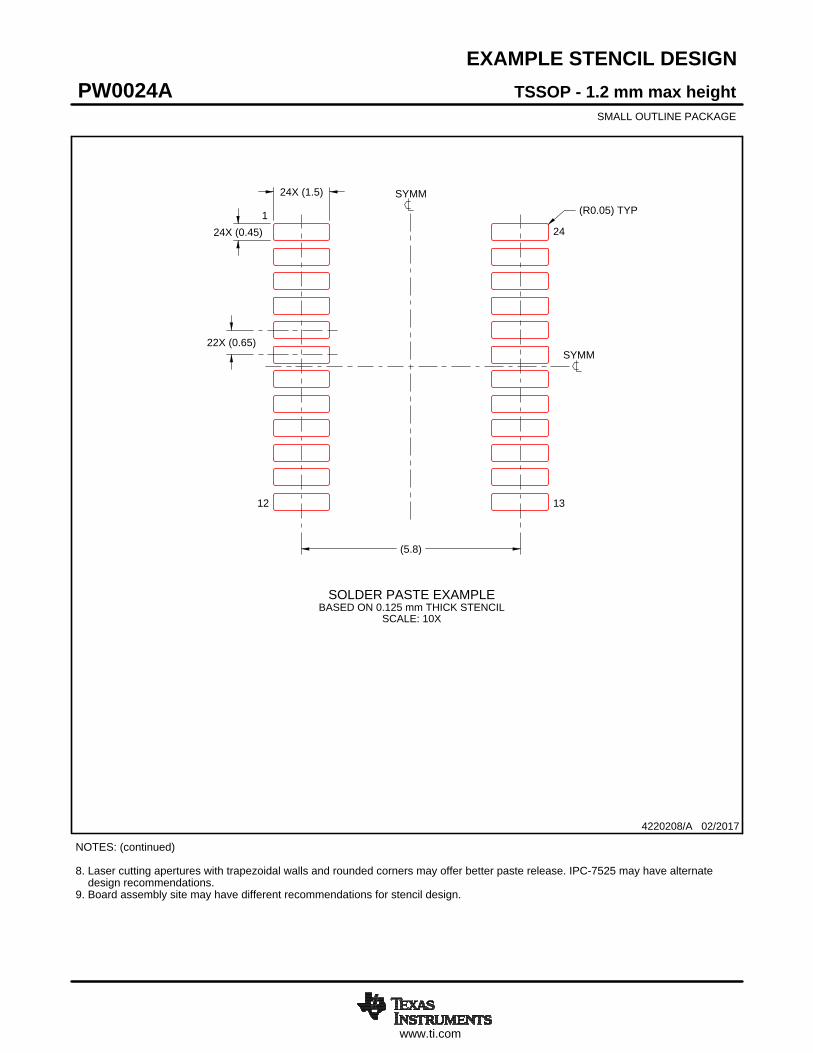
EXAMPLE STENCIL DESIGN
24X (1.5)
24X (0.45)
22X (0.65)
(5.8)
(R0.05) TYP
TSSOP - 1.2 mm max heightPW0024ASMALL OUTLINE PACKAGE
4220208/A 02/2017
NOTES: (continued) 8. Laser cutting apertures with trapezoidal walls and rounded corners may offer better paste release. IPC-7525 may have alternate design recommendations. 9. Board assembly site may have different recommendations for stencil design.
SOLDER PASTE EXAMPLEBASED ON 0.125 mm THICK STENCIL
SCALE: 10X
SYMM
SYMM
1
12 13
24

NOTES:
1. All linear dimensions are in millimeters. Any dimensions in parenthesis are for reference only. Dimensioning and tolerancingper ASME Y14.5M.
2. This drawing is subject to change without notice.3. The package thermal pad must be soldered to the printed circuit board for optimal thermal and mechanical performance.
PACKAGE OUTLINE
4225250/A 09/2019
www.ti.com
VQFN - 1 mm max height
PLASTIC QUAD FLATPACK- NO LEAD
RHL0024A
AB
PIN 1 INDEX AREA
3.63.4
5.65.4
0.08 C
SEATING PLANE
C1 MAX
(0.1) TYP
0.050.00
0.1 C A B0.05 C
SYMM
SYMM
1PIN 1 ID(OPTIONAL)
2.05±0.1
4.05±0.1
2X (0.55)
2X4.5
18X 0.5
2
11
12 13
14
23
24
2X 1.5
4X (0.2)
24X 0.300.18
24X 0.50.3
21
AutoCAD SHX Text
AutoCAD SHX Text

NOTES: (continued)
4. This package is designed to be soldered to a thermal pad on the board. For more information, see Texas Instruments literaturenumber SLUA271 (www.ti.com/lit/slua271).
5. Vias are optional depending on application, refer to device data sheet. If any vias are implemented, refer to their locations shown on this view. It is recommended that vias under paste be filled, plugged or tented.
EXAMPLE BOARD LAYOUT
4225250/A 09/2019
www.ti.com
VQFN - 1 mm max height
RHL0024A
PLASTIC QUAD FLATPACK- NO LEAD
LAND PATTERN EXAMPLEEXPOSED METAL SHOWN
SCALE: 18X
SYMM
SYMM2X (1.5)
6X (0.67)
4X(0.775)
(5.3)
(3.3)
24X (0.6)
24X (0.24)
18X (0.5)
(4.05)
(2.05)
(R0.05) TYP
2
2X (1.105)
2X (0.4)
SOLDER MASKOPENING
METAL UNDERSOLDER MASK
4X (0.2)
2X (0.55)
(Ø 0.2) VIATYP
1 24
11
12 13
14
23
25
4.64.4
0.07 MAXALL AROUND
SOLDER MASK DETAILS
NON SOLDER MASKDEFINED
(PREFERRED)
METAL
SOLDER MASKOPENING
EXPOSED METAL
0.07 MINALL AROUND
SOLDER MASKDEFINED
SOLDER MASKOPENING
METAL UNDERSOLDER MASK
EXPOSED METAL
AutoCAD SHX Text
AutoCAD SHX Text
NOTES: (continued)
6. Laser cutting apertures with trapezoidal walls and rounded corners may offer better paste release. IPC-7525 may have alternatedesign recommendations.
EXAMPLE STENCIL DESIGN
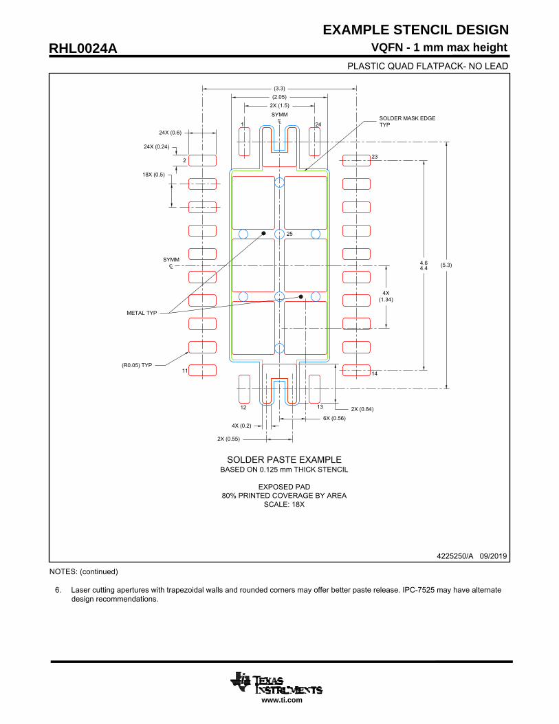
4225250/A 09/2019
www.ti.com
VQFN - 1 mm max height
RHL0024A
PLASTIC QUAD FLATPACK- NO LEAD
SOLDER PASTE EXAMPLEBASED ON 0.125 mm THICK STENCIL
EXPOSED PAD80% PRINTED COVERAGE BY AREA
SCALE: 18X
SYMM
SYMM2X (1.5)
4X(1.34)
6X (0.56)
(5.3)
(3.3)
24X (0.6)
24X (0.24)
18X (0.5)
(2.05)
(R0.05) TYP
2
2X (0.84)
METAL TYP
4X (0.2)
2X (0.55)
1 24
11
12 13
14
23
25
4.64.4
SOLDER MASK EDGETYP
AutoCAD SHX Text
AutoCAD SHX Text

IMPORTANT NOTICE AND DISCLAIMER
TI PROVIDES TECHNICAL AND RELIABILITY DATA (INCLUDING DATASHEETS), DESIGN RESOURCES (INCLUDING REFERENCE DESIGNS), APPLICATION OR OTHER DESIGN ADVICE, WEB TOOLS, SAFETY INFORMATION, AND OTHER RESOURCES “AS IS” AND WITH ALL FAULTS, AND DISCLAIMS ALL WARRANTIES, EXPRESS AND IMPLIED, INCLUDING WITHOUT LIMITATION ANY IMPLIED WARRANTIES OF MERCHANTABILITY, FITNESS FOR A PARTICULAR PURPOSE OR NON-INFRINGEMENT OF THIRD PARTY INTELLECTUAL PROPERTY RIGHTS.These resources are intended for skilled developers designing with TI products. You are solely responsible for (1) selecting the appropriate TI products for your application, (2) designing, validating and testing your application, and (3) ensuring your application meets applicable standards, and any other safety, security, or other requirements. These resources are subject to change without notice. TI grants you permission to use these resources only for development of an application that uses the TI products described in the resource. Other reproduction and display of these resources is prohibited. No license is granted to any other TI intellectual property right or to any third party intellectual property right. TI disclaims responsibility for, and you will fully indemnify TI and its representatives against, any claims, damages, costs, losses, and liabilities arising out of your use of these resources.TI’s products are provided subject to TI’s Terms of Sale (www.ti.com/legal/termsofsale.html) or other applicable terms available either on ti.com or provided in conjunction with such TI products. TI’s provision of these resources does not expand or otherwise alter TI’s applicable warranties or warranty disclaimers for TI products.
Mailing Address: Texas Instruments, Post Office Box 655303, Dallas, Texas 75265Copyright © 2020, Texas Instruments Incorporated
Related Documents