B DIR 5 4 A 3 V CCA V CCB Product Folder Sample & Buy Technical Documents Tools & Software Support & Community SN74LVC1T45 SCES515K – DECEMBER 2003 – REVISED DECEMBER 2014 SN74LVC1T45 Single-Bit Dual-Supply Bus Transceiver With Configurable Voltage Translation and 3-State Outputs 1 Features 3 Description This single-bit noninverting bus transceiver uses two 1• Available in the Texas Instruments NanoFree™ separate configurable power-supply rails. The A port Package is designed to track V CCA .V CCA accepts any supply • Fully Configurable Dual-Rail Design Allows Each voltage from 1.65 V to 5.5 V. The B port is designed Port to Operate Over the Full 1.65-V to 5.5-V to track V CCB .V CCB accepts any supply voltage from Power-Supply Range 1.65 V to 5.5 V. This allows for universal low-voltage bidirectional translation between any of the 1.8-V, • V CC Isolation Feature – If Either V CC Input Is at 2.5-V, 3.3-V, and 5-V voltage nodes. GND, Both Ports Are in the High-Impedance State • DIR Input Circuit Referenced to V CCA The SN74LVC1T45 is designed for asynchronous communication between two data buses. The logic • Low Power Consumption, 4-μA Max I CC levels of the direction-control (DIR) input activate • ±24-mA Output Drive at 3.3 V either the B-port outputs or the A-port outputs. The • I off Supports Partial-Power-Down Mode Operation device transmits data from the A bus to the B bus when the B-port outputs are activated and from the B • Max Data Rates bus to the A bus when the A-port outputs are – 420 Mbps (3.3-V to 5-V Translation) activated. The input circuitry on both A and B ports – 210 Mbps (Translate to 3.3 V) always is active and must have a logic HIGH or LOW level applied to prevent excess I CC and I CCZ . – 140 Mbps (Translate to 2.5 V) – 75 Mbps (Translate to 1.8 V) Device Information (1) • Latch-Up Performance Exceeds 100 mA Per PART NUMBER PACKAGE BODY SIZE (NOM) JESD 78, Class II 2.90 mm × 1.60 mm • ESD Protection Exceeds JESD 22 SOT (6) 2.00 mm × 1.25 mm SN74LVC1T45 – 2000-V Human-Body Model (A114-A) 1.60 mm × 1.20 mm – 200-V Machine Model (A115-A) DSBGA (6) 1.39 mm × 0.90 mm – 1000-V Charged-Device Model (C101) (1) For all available packages, see the orderable addendum at the end of the datasheet. 2 Applications • Personal Electronic • Industrial • Enterprise • Telecom Functional Block Diagram 1 An IMPORTANT NOTICE at the end of this data sheet addresses availability, warranty, changes, use in safety-critical applications, intellectual property matters and other important disclaimers. PRODUCTION DATA.

Welcome message from author
This document is posted to help you gain knowledge. Please leave a comment to let me know what you think about it! Share it to your friends and learn new things together.
Transcript

B
DIR5
4
A3
VCCA VCCB
Product
Folder
Sample &Buy
Technical
Documents
Tools &
Software
Support &Community
SN74LVC1T45SCES515K –DECEMBER 2003–REVISED DECEMBER 2014
SN74LVC1T45 Single-Bit Dual-Supply Bus Transceiver With Configurable VoltageTranslation and 3-State Outputs
1 Features 3 DescriptionThis single-bit noninverting bus transceiver uses two
1• Available in the Texas Instruments NanoFree™separate configurable power-supply rails. The A portPackageis designed to track VCCA. VCCA accepts any supply
• Fully Configurable Dual-Rail Design Allows Each voltage from 1.65 V to 5.5 V. The B port is designedPort to Operate Over the Full 1.65-V to 5.5-V to track VCCB. VCCB accepts any supply voltage fromPower-Supply Range 1.65 V to 5.5 V. This allows for universal low-voltage
bidirectional translation between any of the 1.8-V,• VCC Isolation Feature – If Either VCC Input Is at2.5-V, 3.3-V, and 5-V voltage nodes.GND, Both Ports Are in the High-Impedance State
• DIR Input Circuit Referenced to VCCA The SN74LVC1T45 is designed for asynchronouscommunication between two data buses. The logic• Low Power Consumption, 4-μA Max ICC levels of the direction-control (DIR) input activate• ±24-mA Output Drive at 3.3 V either the B-port outputs or the A-port outputs. The
• Ioff Supports Partial-Power-Down Mode Operation device transmits data from the A bus to the B buswhen the B-port outputs are activated and from the B• Max Data Ratesbus to the A bus when the A-port outputs are– 420 Mbps (3.3-V to 5-V Translation) activated. The input circuitry on both A and B ports
– 210 Mbps (Translate to 3.3 V) always is active and must have a logic HIGH or LOWlevel applied to prevent excess ICC and ICCZ.– 140 Mbps (Translate to 2.5 V)
– 75 Mbps (Translate to 1.8 V) Device Information(1)• Latch-Up Performance Exceeds 100 mA Per
PART NUMBER PACKAGE BODY SIZE (NOM)JESD 78, Class II2.90 mm × 1.60 mm
• ESD Protection Exceeds JESD 22SOT (6) 2.00 mm × 1.25 mm
SN74LVC1T45– 2000-V Human-Body Model (A114-A) 1.60 mm × 1.20 mm– 200-V Machine Model (A115-A) DSBGA (6) 1.39 mm × 0.90 mm– 1000-V Charged-Device Model (C101) (1) For all available packages, see the orderable addendum at
the end of the datasheet.2 Applications• Personal Electronic• Industrial• Enterprise• Telecom
Functional Block Diagram
1
An IMPORTANT NOTICE at the end of this data sheet addresses availability, warranty, changes, use in safety-critical applications,intellectual property matters and other important disclaimers. PRODUCTION DATA.
SN74LVC1T45SCES515K –DECEMBER 2003–REVISED DECEMBER 2014 www.ti.com
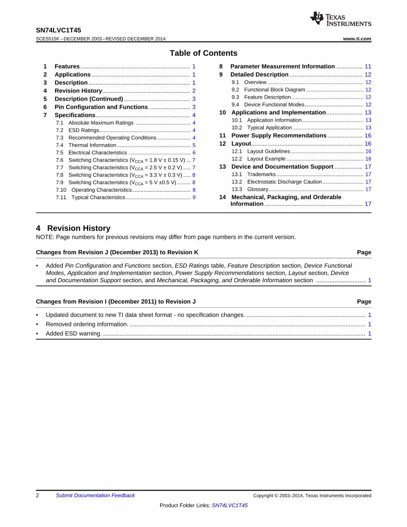
Table of Contents1 Features .................................................................. 1 8 Parameter Measurement Information ................ 112 Applications ........................................................... 1 9 Detailed Description ............................................ 12
9.1 Overview ................................................................. 123 Description ............................................................. 19.2 Functional Block Diagram ....................................... 124 Revision History..................................................... 29.3 Feature Description................................................. 125 Description (Continued) ........................................ 39.4 Device Functional Modes........................................ 126 Pin Configuration and Functions ......................... 3
10 Applications and Implementation...................... 137 Specifications......................................................... 410.1 Application Information.......................................... 137.1 Absolute Maximum Ratings ..................................... 410.2 Typical Application ................................................ 137.2 ESD Ratings.............................................................. 4
11 Power Supply Recommendations ..................... 167.3 Recommended Operating Conditions....................... 412 Layout................................................................... 167.4 Thermal Information .................................................. 5
12.1 Layout Guidelines ................................................. 167.5 Electrical Characteristics .......................................... 612.2 Layout Example .................................................... 167.6 Switching Characteristics (VCCA = 1.8 V ± 0.15 V) ... 7
13 Device and Documentation Support ................. 177.7 Switching Characteristics (VCCA = 2.5 V ± 0.2 V) ..... 713.1 Trademarks ........................................................... 177.8 Switching Characteristics (VCCA = 3.3 V ± 0.3 V) ..... 813.2 Electrostatic Discharge Caution............................ 177.9 Switching Characteristics (VCCA = 5 V ±0.5 V) ......... 813.3 Glossary ................................................................ 177.10 Operating Characteristics........................................ 8
7.11 Typical Characteristics ............................................ 9 14 Mechanical, Packaging, and OrderableInformation ........................................................... 17
4 Revision HistoryNOTE: Page numbers for previous revisions may differ from page numbers in the current version.
Changes from Revision J (December 2013) to Revision K Page
• Added Pin Configuration and Functions section, ESD Ratings table, Feature Description section, Device FunctionalModes, Application and Implementation section, Power Supply Recommendations section, Layout section, Deviceand Documentation Support section, and Mechanical, Packaging, and Orderable Information section .............................. 1
Changes from Revision I (December 2011) to Revision J Page
• Updated document to new TI data sheet format - no specification changes. ........................................................................ 1• Removed ordering information. .............................................................................................................................................. 1• Added ESD warning. .............................................................................................................................................................. 1
2 Submit Documentation Feedback Copyright © 2003–2014, Texas Instruments Incorporated
Product Folder Links: SN74LVC1T45

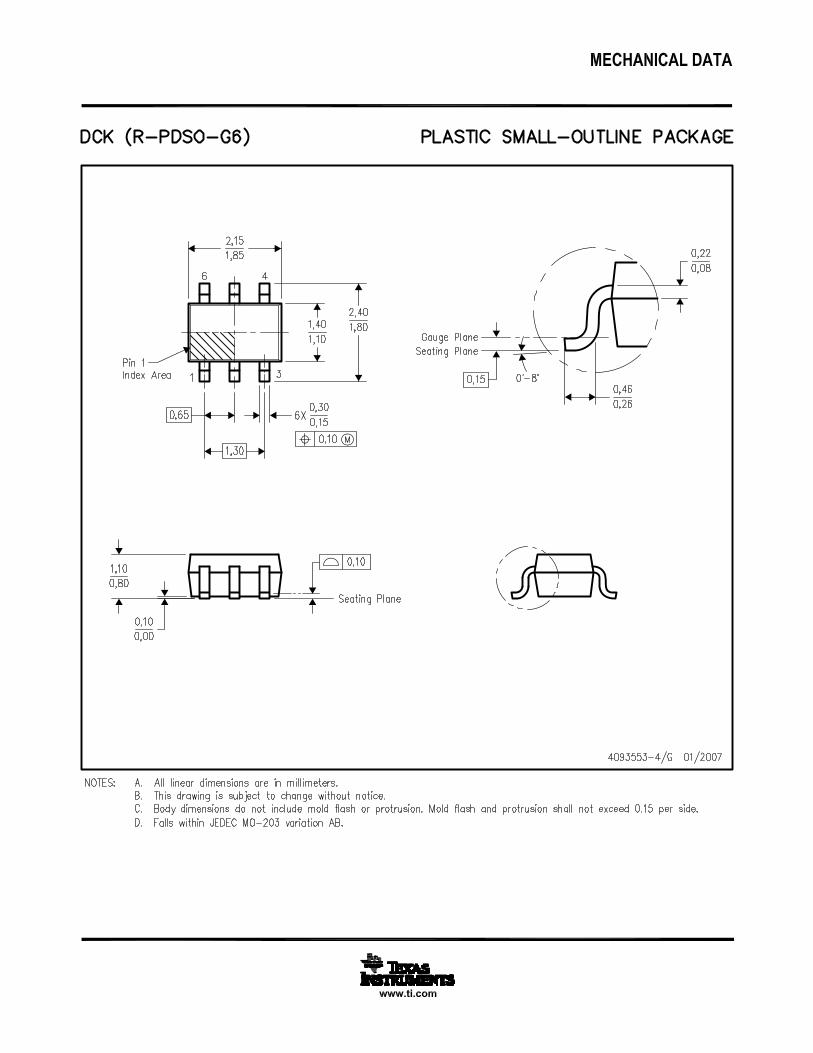
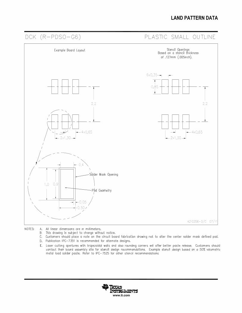
DBV PACKAGE(TOP VIEW)
DCK PACKAGE(TOP VIEW)
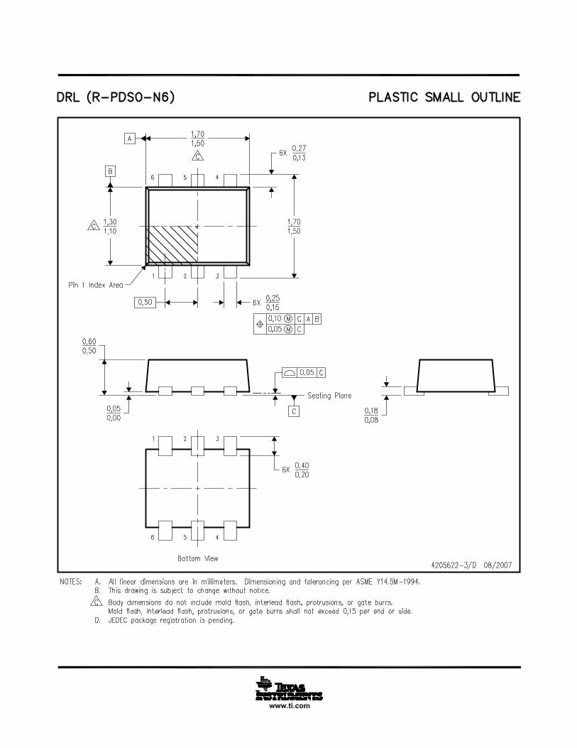
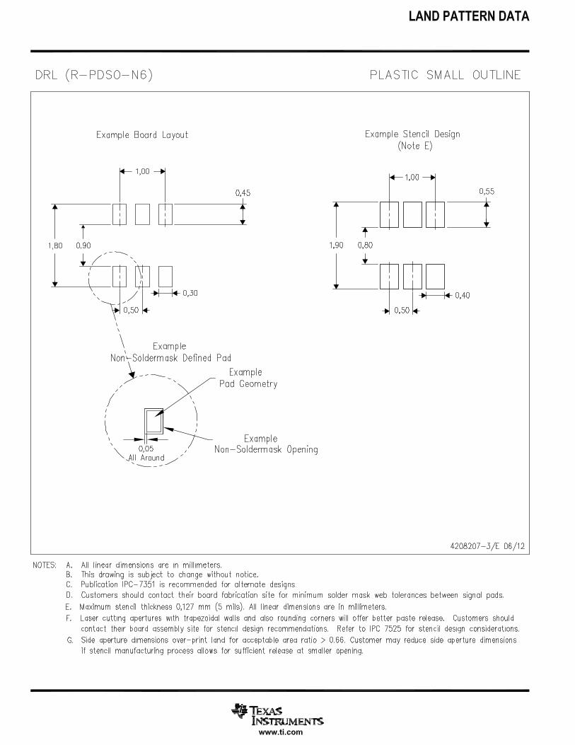
DRL PACKAGE(TOP VIEW)
YZP PACKAGE(BOTTOM VIEW)
SN74LVC1T45www.ti.com SCES515K –DECEMBER 2003–REVISED DECEMBER 2014
5 Description (Continued)The SN74LVC1T45 is designed so that the DIR input is powered by VCCA.
This device is fully specified for partial-power-down applications using Ioff. The Ioff circuitry disables the outputs,preventing damaging current backflow through the device when it is powered down.
The VCC isolation feature ensures that if either VCC input is at GND, then both ports are in the high-impedancestate.
NanoFree package technology is a major breakthrough in IC packaging concepts, using the die as the package.
6 Pin Configuration and Functions
Pin FunctionsPIN
I/O DESCRIPTIONNAME NO.VCCA 1 p SYSTEM-1 supply voltage (1.65 V to 5.5 V)GND 2 G Device GND
A 3 I/O Output level depends on VCC1 voltage.B 4 I/O Input threshold value depends on VCC2 voltage.
DIR 5 I GND (low level) determines B-port to A-port direction.VCCB 6 P SYSTEM-2 supply voltage (1.65 V to 5.5 V)
Copyright © 2003–2014, Texas Instruments Incorporated Submit Documentation Feedback 3
Product Folder Links: SN74LVC1T45
SN74LVC1T45SCES515K –DECEMBER 2003–REVISED DECEMBER 2014 www.ti.com
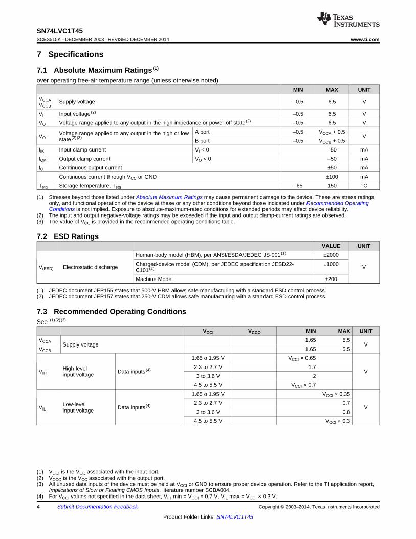
7 Specifications
7.1 Absolute Maximum Ratings (1)
over operating free-air temperature range (unless otherwise noted)MIN MAX UNIT
VCCA Supply voltage –0.5 6.5 VVCCB
VI Input voltage (2) –0.5 6.5 VVO Voltage range applied to any output in the high-impedance or power-off state (2) –0.5 6.5 V
A port –0.5 VCCA + 0.5Voltage range applied to any output in the high or lowVO Vstate (2) (3) B port –0.5 VCCB + 0.5IIK Input clamp current VI < 0 –50 mAIOK Output clamp current VO < 0 –50 mAIO Continuous output current ±50 mA
Continuous current through VCC or GND ±100 mATstg Storage temperature, Tstg –65 150 °C
(1) Stresses beyond those listed under Absolute Maximum Ratings may cause permanent damage to the device. These are stress ratingsonly, and functional operation of the device at these or any other conditions beyond those indicated under Recommended OperatingConditions is not implied. Exposure to absolute-maximum-rated conditions for extended periods may affect device reliability.
(2) The input and output negative-voltage ratings may be exceeded if the input and output clamp-current ratings are observed.(3) The value of VCC is provided in the recommended operating conditions table.
7.2 ESD RatingsVALUE UNIT
Human-body model (HBM), per ANSI/ESDA/JEDEC JS-001 (1) ±2000Charged-device model (CDM), per JEDEC specification JESD22- ±1000V(ESD) Electrostatic discharge VC101 (2)
Machine Model ±200
(1) JEDEC document JEP155 states that 500-V HBM allows safe manufacturing with a standard ESD control process.(2) JEDEC document JEP157 states that 250-V CDM allows safe manufacturing with a standard ESD control process.
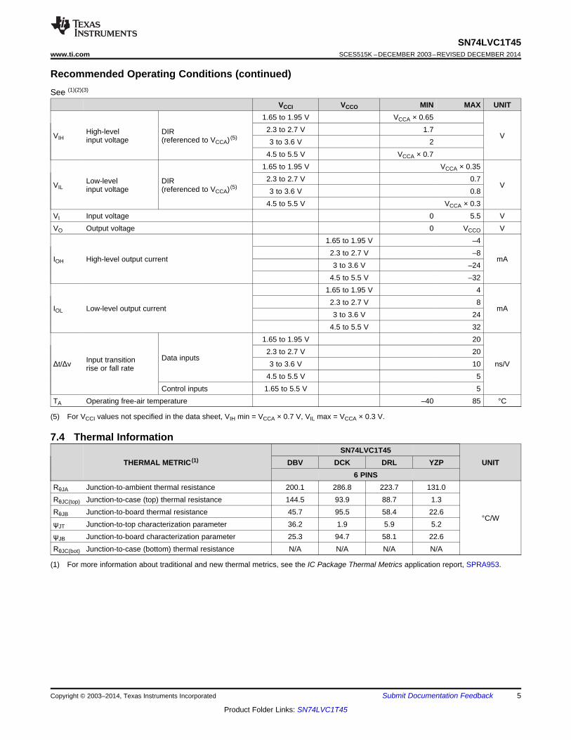
7.3 Recommended Operating ConditionsSee (1) (2) (3)
VCCI VCCO MIN MAX UNITVCCA 1.65 5.5
Supply voltage VVCCB 1.65 5.5
1.65 o 1.95 V VCCI × 0.652.3 to 2.7 V 1.7High-levelVIH Data inputs (4) Vinput voltage 3 to 3.6 V 24.5 to 5.5 V VCCI × 0.7
1.65 o 1.95 V VCCI × 0.352.3 to 2.7 V 0.7Low-levelVIL Data inputs (4) Vinput voltage 3 to 3.6 V 0.84.5 to 5.5 V VCCI × 0.3
(1) VCCI is the VCC associated with the input port.(2) VCCO is the VCC associated with the output port.(3) All unused data inputs of the device must be held at VCCI or GND to ensure proper device operation. Refer to the TI application report,
Implications of Slow or Floating CMOS Inputs, literature number SCBA004.(4) For VCCI values not specified in the data sheet, VIH min = VCCI × 0.7 V, VIL max = VCCI × 0.3 V.
4 Submit Documentation Feedback Copyright © 2003–2014, Texas Instruments Incorporated
Product Folder Links: SN74LVC1T45
SN74LVC1T45www.ti.com SCES515K –DECEMBER 2003–REVISED DECEMBER 2014
Recommended Operating Conditions (continued)See (1)(2)(3)
VCCI VCCO MIN MAX UNIT1.65 to 1.95 V VCCA × 0.652.3 to 2.7 V 1.7High-level DIRVIH Vinput voltage (referenced to VCCA) (5) 3 to 3.6 V 24.5 to 5.5 V VCCA × 0.7
1.65 to 1.95 V VCCA × 0.352.3 to 2.7 V 0.7Low-level DIRVIL Vinput voltage (referenced to VCCA)(5) 3 to 3.6 V 0.84.5 to 5.5 V VCCA × 0.3
VI Input voltage 0 5.5 VVO Output voltage 0 VCCO V
1.65 to 1.95 V –42.3 to 2.7 V –8
IOH High-level output current mA3 to 3.6 V –24
4.5 to 5.5 V –321.65 to 1.95 V 4
2.3 to 2.7 V 8IOL Low-level output current mA
3 to 3.6 V 244.5 to 5.5 V 32
1.65 to 1.95 V 202.3 to 2.7 V 20
Data inputsInput transitionΔt/Δv 3 to 3.6 V 10 ns/Vrise or fall rate4.5 to 5.5 V 5
Control inputs 1.65 to 5.5 V 5TA Operating free-air temperature –40 85 °C
(5) For VCCI values not specified in the data sheet, VIH min = VCCA × 0.7 V, VIL max = VCCA × 0.3 V.
7.4 Thermal InformationSN74LVC1T45
THERMAL METRIC (1) DBV DCK DRL YZP UNIT6 PINS
RθJA Junction-to-ambient thermal resistance 200.1 286.8 223.7 131.0RθJC(top) Junction-to-case (top) thermal resistance 144.5 93.9 88.7 1.3RθJB Junction-to-board thermal resistance 45.7 95.5 58.4 22.6
°C/WψJT Junction-to-top characterization parameter 36.2 1.9 5.9 5.2ψJB Junction-to-board characterization parameter 25.3 94.7 58.1 22.6RθJC(bot) Junction-to-case (bottom) thermal resistance N/A N/A N/A N/A
(1) For more information about traditional and new thermal metrics, see the IC Package Thermal Metrics application report, SPRA953.
Copyright © 2003–2014, Texas Instruments Incorporated Submit Documentation Feedback 5
Product Folder Links: SN74LVC1T45
SN74LVC1T45SCES515K –DECEMBER 2003–REVISED DECEMBER 2014 www.ti.com
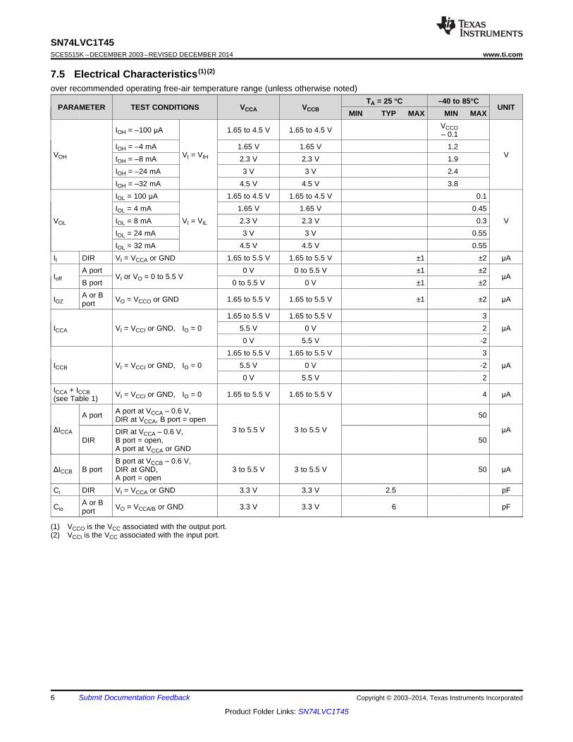
7.5 Electrical Characteristics (1) (2)
over recommended operating free-air temperature range (unless otherwise noted)TA = 25 °C –40 to 85°C
PARAMETER TEST CONDITIONS VCCA VCCB UNITMIN TYP MAX MIN MAX
VCCOIOH = –100 μA 1.65 to 4.5 V 1.65 to 4.5 V – 0.1IOH = –4 mA 1.65 V 1.65 V 1.2
VOH VI = VIH VIOH = –8 mA 2.3 V 2.3 V 1.9IOH = –24 mA 3 V 3 V 2.4IOH = –32 mA 4.5 V 4.5 V 3.8IOL = 100 μA 1.65 to 4.5 V 1.65 to 4.5 V 0.1IOL = 4 mA 1.65 V 1.65 V 0.45
VOL IOL = 8 mA VI = VIL 2.3 V 2.3 V 0.3 VIOL = 24 mA 3 V 3 V 0.55IOL = 32 mA 4.5 V 4.5 V 0.55
II DIR VI = VCCA or GND 1.65 to 5.5 V 1.65 to 5.5 V ±1 ±2 μAA port 0 V 0 to 5.5 V ±1 ±2
Ioff VI or VO = 0 to 5.5 V μAB port 0 to 5.5 V 0 V ±1 ±2A or BIOZ VO = VCCO or GND 1.65 to 5.5 V 1.65 to 5.5 V ±1 ±2 μAport
1.65 to 5.5 V 1.65 to 5.5 V 3ICCA VI = VCCI or GND, IO = 0 5.5 V 0 V 2 μA
0 V 5.5 V -21.65 to 5.5 V 1.65 to 5.5 V 3
ICCB VI = VCCI or GND, IO = 0 5.5 V 0 V -2 μA0 V 5.5 V 2
ICCA + ICCB VI = VCCI or GND, IO = 0 1.65 to 5.5 V 1.65 to 5.5 V 4 μA(see Table 1)A port at VCCA – 0.6 V,A port 50DIR at VCCA, B port = open
ΔICCA 3 to 5.5 V 3 to 5.5 V μADIR at VCCA – 0.6 V,DIR B port = open, 50
A port at VCCA or GNDB port at VCCB – 0.6 V,
ΔICCB B port DIR at GND, 3 to 5.5 V 3 to 5.5 V 50 μAA port = open
Ci DIR VI = VCCA or GND 3.3 V 3.3 V 2.5 pFA or BCio VO = VCCA/B or GND 3.3 V 3.3 V 6 pFport
(1) VCCO is the VCC associated with the output port.(2) VCCI is the VCC associated with the input port.
6 Submit Documentation Feedback Copyright © 2003–2014, Texas Instruments Incorporated
Product Folder Links: SN74LVC1T45

SN74LVC1T45www.ti.com SCES515K –DECEMBER 2003–REVISED DECEMBER 2014
7.6 Switching Characteristics (VCCA = 1.8 V ± 0.15 V)over recommended operating free-air temperature range, VCCA = 1.8 V ± 0.15 V (see Figure 9)
VCCB = 1.8 V VCCB = 2.5 V VCCB = 3.3 V VCCB = 5 VFROM TO ±0.15 V ±0.2 V ±0.3 V ±0.5 VPARAMETER UNIT(INPUT) (OUTPUT)
MIN MAX MIN MAX MIN MAX MIN MAXtPLH 3 17.7 2.2 10.3 1.7 8.3 1.4 7.2
A B nstPHL 2.8 14.3 2.2 8.5 1.8 7.1 1.7 7tPLH 3 17.7 2.3 16 2.1 15.5 1.9 15.1
B A nstPHL 2.8 14.3 2.1 12.9 2 12.6 1.8 12.2tPHZ 5.2 19.4 4.8 18.5 4.7 18.4 5.1 17.1
DIR A nstPLZ 2.3 10.5 2.1 10.5 2.4 10.7 3.1 10.9tPHZ 7.4 21.9 4.9 11.5 4.6 10.3 2.8 8.2
DIR B nstPLZ 4.2 16 3.7 9.2 3.3 8.4 2.4 6.4
tPZH(1) 33.7 25.2 23.9 21.5
DIR A nstPZL
(1) 36.2 24.4 22.9 20.4tPZH
(1) 28.2 20.8 19 18.1DIR B ns
tPZL(1) 33.7 27 25.5 24.1
(1) The enable time is a calculated value, derived using the formula shown in the Enable Times section.
7.7 Switching Characteristics (VCCA = 2.5 V ± 0.2 V)over recommended operating free-air temperature range, VCCA = 2.5 V ± 0.2 V (see Figure 9)
VCCB = 1.8 V VCCB = 2.5 V VCCB = 3.3 V VCCB = 5 VFROM TO ±0.15 V ±0.2 V ±0.3 V ±0.5 VPARAMETER UNIT(INPUT) (OUTPUT)
MIN MAX MIN MAX MIN MAX MIN MAXtPLH 2.3 16 1.5 8.5 1.3 6.4 1.1 5.1
A B nstPHL 2.1 12.9 1.4 7.5 1.3 5.4 0.9 4.6tPLH 2.2 10.3 1.5 8.5 1.4 8 1 7.5
B A nstPHL 2.2 8.5 1.4 7.5 1.3 7 0.9 6.2tPHZ 3 8.1 3.1 8.1 2.8 8.1 3.2 8.1
DIR A nstPLZ 1.3 5.9 1.3 5.9 1.3 5.9 1 5.8tPHZ 6.5 23.7 4.1 11.4 3.9 10.2 2.4 7.1
DIR B nstPLZ 3.9 18.9 3.2 9.6 2.8 8.4 1.8 5.3
tPZH(1) 29.2 18.1 16.4 12.8
DIR A nstPZL
(1) 32.2 18.9 17.2 13.3tPZH
(1) 21.9 14.4 12.3 10.9DIR B ns
tPZL(1) 21 15.6 13.5 12.7
(1) The enable time is a calculated value, derived using the formula shown in the Enable Times section.
Copyright © 2003–2014, Texas Instruments Incorporated Submit Documentation Feedback 7
Product Folder Links: SN74LVC1T45
SN74LVC1T45SCES515K –DECEMBER 2003–REVISED DECEMBER 2014 www.ti.com
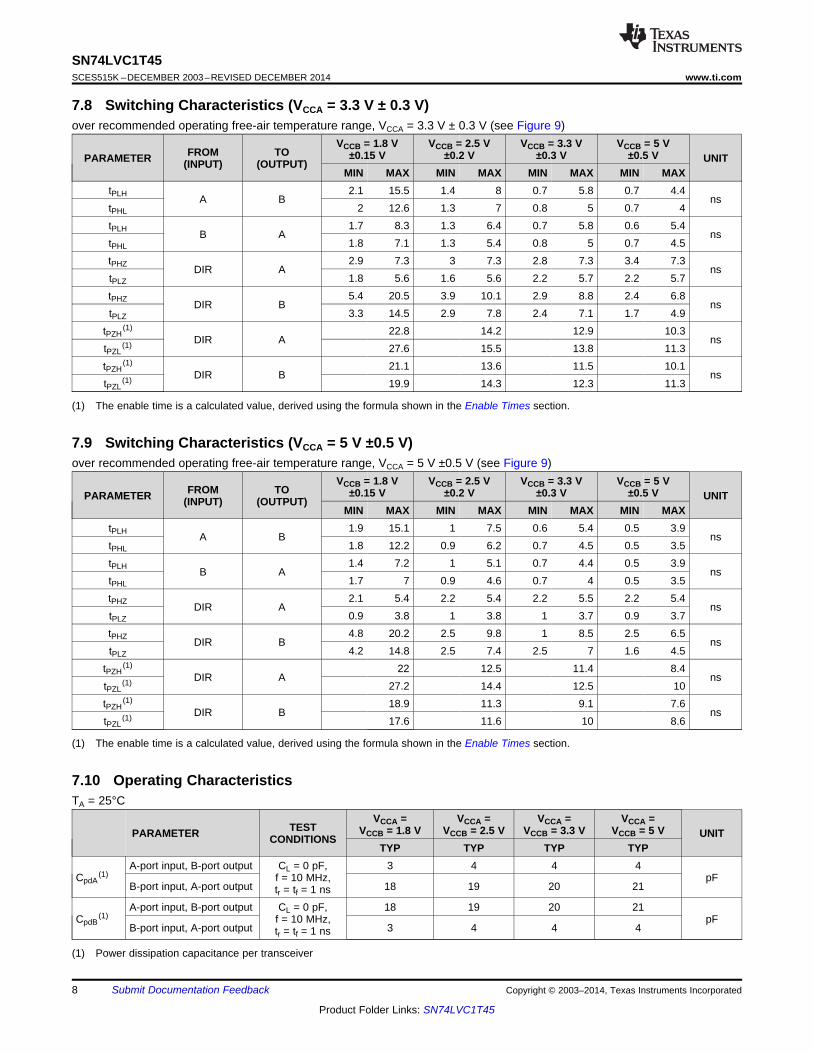
7.8 Switching Characteristics (VCCA = 3.3 V ± 0.3 V)over recommended operating free-air temperature range, VCCA = 3.3 V ± 0.3 V (see Figure 9)
VCCB = 1.8 V VCCB = 2.5 V VCCB = 3.3 V VCCB = 5 VFROM TO ±0.15 V ±0.2 V ±0.3 V ±0.5 VPARAMETER UNIT(INPUT) (OUTPUT)
MIN MAX MIN MAX MIN MAX MIN MAXtPLH 2.1 15.5 1.4 8 0.7 5.8 0.7 4.4
A B nstPHL 2 12.6 1.3 7 0.8 5 0.7 4tPLH 1.7 8.3 1.3 6.4 0.7 5.8 0.6 5.4
B A nstPHL 1.8 7.1 1.3 5.4 0.8 5 0.7 4.5tPHZ 2.9 7.3 3 7.3 2.8 7.3 3.4 7.3
DIR A nstPLZ 1.8 5.6 1.6 5.6 2.2 5.7 2.2 5.7tPHZ 5.4 20.5 3.9 10.1 2.9 8.8 2.4 6.8
DIR B nstPLZ 3.3 14.5 2.9 7.8 2.4 7.1 1.7 4.9
tPZH(1) 22.8 14.2 12.9 10.3
DIR A nstPZL
(1) 27.6 15.5 13.8 11.3tPZH
(1) 21.1 13.6 11.5 10.1DIR B ns
tPZL(1) 19.9 14.3 12.3 11.3
(1) The enable time is a calculated value, derived using the formula shown in the Enable Times section.
7.9 Switching Characteristics (VCCA = 5 V ±0.5 V)over recommended operating free-air temperature range, VCCA = 5 V ±0.5 V (see Figure 9)
VCCB = 1.8 V VCCB = 2.5 V VCCB = 3.3 V VCCB = 5 VFROM TO ±0.15 V ±0.2 V ±0.3 V ±0.5 VPARAMETER UNIT(INPUT) (OUTPUT)
MIN MAX MIN MAX MIN MAX MIN MAXtPLH 1.9 15.1 1 7.5 0.6 5.4 0.5 3.9
A B nstPHL 1.8 12.2 0.9 6.2 0.7 4.5 0.5 3.5tPLH 1.4 7.2 1 5.1 0.7 4.4 0.5 3.9
B A nstPHL 1.7 7 0.9 4.6 0.7 4 0.5 3.5tPHZ 2.1 5.4 2.2 5.4 2.2 5.5 2.2 5.4
DIR A nstPLZ 0.9 3.8 1 3.8 1 3.7 0.9 3.7tPHZ 4.8 20.2 2.5 9.8 1 8.5 2.5 6.5
DIR B nstPLZ 4.2 14.8 2.5 7.4 2.5 7 1.6 4.5
tPZH(1) 22 12.5 11.4 8.4
DIR A nstPZL
(1) 27.2 14.4 12.5 10tPZH
(1) 18.9 11.3 9.1 7.6DIR B ns
tPZL(1) 17.6 11.6 10 8.6
(1) The enable time is a calculated value, derived using the formula shown in the Enable Times section.
7.10 Operating CharacteristicsTA = 25°C
VCCA = VCCA = VCCA = VCCA =TEST VCCB = 1.8 V VCCB = 2.5 V VCCB = 3.3 V VCCB = 5 VPARAMETER UNITCONDITIONS
TYP TYP TYP TYPA-port input, B-port output CL = 0 pF, 3 4 4 4
CpdA(1) f = 10 MHz, pF
B-port input, A-port output 18 19 20 21tr = tf = 1 nsA-port input, B-port output CL = 0 pF, 18 19 20 21
CpdB(1) f = 10 MHz, pF
B-port input, A-port output 3 4 4 4tr = tf = 1 ns
(1) Power dissipation capacitance per transceiver
8 Submit Documentation Feedback Copyright © 2003–2014, Texas Instruments Incorporated
Product Folder Links: SN74LVC1T45
0 5 10 15 20 25 30 35
tP
HL
−n
s
CL − pF
0
1
2
3
4
5
6
7
8
9
10
0
1
2
3
4
5
6
7
8
9
10
0 5 10 15 20 25 30 35
tP
LH
−n
s
CL − pF
0 5 10 15 20 25 30 35
t PH
L−
ns
CL − pF
0
1
2
3
4
5
6
7
8
9
10
0
1
2
3
4
5
6
7
8
9
10
0 5 10 15 20 25 30 35
tP
LH
−n
s
CL − pF
0
1
2
3
4
5
6
7
8
9
0 5 10 15 20 25 30 35
tP
HL
−n
s
CL − pF
10
0
1
2
3
4
5
6
7
8
9
10
0 5 10 15 20 25 30 35
tP
LH
−n
s
CL − pF
SN74LVC1T45www.ti.com SCES515K –DECEMBER 2003–REVISED DECEMBER 2014
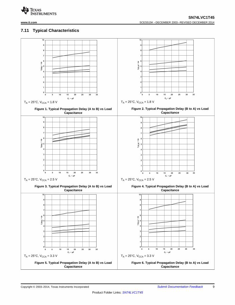
7.11 Typical Characteristics
TA = 25°C, VCCA = 1.8 VTA = 25°C, VCCA = 1.8 V
Figure 2. Typical Propagation Delay (B to A) vs LoadFigure 1. Typical Propagation Delay (A to B) vs LoadCapacitanceCapacitance
TA = 25°C, VCCA = 2.5 V TA = 25°C, VCCA = 2.5 V
Figure 3. Typical Propagation Delay (A to B) vs Load Figure 4. Typical Propagation Delay (B to A) vs LoadCapacitance Capacitance
TA = 25°C, VCCA = 3.3 V TA = 25°C, VCCA = 3.3 V
Figure 5. Typical Propagation Delay (A to B) vs Load Figure 6. Typical Propagation Delay (B to A) vs LoadCapacitance Capacitance
Copyright © 2003–2014, Texas Instruments Incorporated Submit Documentation Feedback 9
Product Folder Links: SN74LVC1T45

0 5 10 15 20 25 30 35
tP
LH
−n
s
CL − pF
0
1
2
3
4
5
6
7
8
9
10
0 5 10 15 20 25 30 35
tP
HL
−n
s
CL − pF
0
1
2
3
4
5
6
7
8
9
10
SN74LVC1T45SCES515K –DECEMBER 2003–REVISED DECEMBER 2014 www.ti.com
Typical Characteristics (continued)
TA = 25°C, VCCA = 5 V TA = 25°C, VCCA = 5 V
Figure 7. Typical Propagation Delay (A to B) vs Load Figure 8. Typical Propagation Delay (B to A) vs LoadCapacitance Capacitance
10 Submit Documentation Feedback Copyright © 2003–2014, Texas Instruments Incorporated
Product Folder Links: SN74LVC1T45

VOH
VOL
From Output Under Test
CL(see Note A)
LOAD CIRCUIT
S1
2 × VCCO
Open
GND
RL
RL
tPLH tPHL
OutputControl
(low-levelenabling)
OutputWaveform 1
S1 at 2 × VCCO(see Note B)
OutputWaveform 2
S1 at GND(see Note B)
tPZL
tPZH
tPLZ
tPHZ
VCCA/2VCCA/2
VCCI/2 VCCI/2VCCI
0 V
VCCO/2 VCCO/2VOH
VOL
0 V
VCCO/2 VOL + VTP
VCCO/2VOH − VTP
0 V
VCCI
0 V
VCCI/2 VCCI/2
tw
Input
VCCA
VCCO
VOLTAGE WAVEFORMSPROPAGATION DELAY TIMES
VOLTAGE WAVEFORMSPULSE DURATION
VOLTAGE WAVEFORMSENABLE AND DISABLE TIMES
Output
Input
tpdtPLZ/tPZLtPHZ/tPZH
Open2 × VCCO
GND
TEST S1
NOTES: A. CL includes probe and jig capacitance.B. Waveform 1 is for an output with internal conditions such that the output is low, except when disabled by the output control.
Waveform 2 is for an output with internal conditions such that the output is high, except when disabled by the output control.C. All input pulses are supplied by generators having the following characteristics: PRR 10 MHz, ZO = 50 Ω, dv/dt ≥ 1 V/ns.D. The outputs are measured one at a time, with one transition per measurement.E. tPLZ and tPHZ are the same as tdis.F. tPZL and tPZH are the same as ten.G. tPLH and tPHL are the same as tpd.H. VCCI is the VCC associated with the input port.I. VCCO is the VCC associated with the output port.J. All parameters and waveforms are not applicable to all devices.
1.8 V ± 0.15 V2.5 V ± 0.2 V3.3 V ± 0.3 V5 V ± 0.5 V
2 kΩ2 kΩ2 kΩ2 kΩ
VCCO RL
0.15 V0.15 V0.3 V0.3 V
VTPCL
15 pF15 pF15 pF15 pF
SN74LVC1T45www.ti.com SCES515K –DECEMBER 2003–REVISED DECEMBER 2014
8 Parameter Measurement Information
Figure 9. Load Circuit and Voltage Waveforms
Copyright © 2003–2014, Texas Instruments Incorporated Submit Documentation Feedback 11
Product Folder Links: SN74LVC1T45
B
DIR5
4
A3
VCCA VCCB
SN74LVC1T45SCES515K –DECEMBER 2003–REVISED DECEMBER 2014 www.ti.com
9 Detailed Description
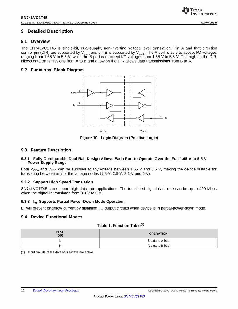
9.1 OverviewThe SN74LVC1T45 is single-bit, dual-supply, non-inverting voltage level translation. Pin A and that directioncontrol pin (DIR) are supported by VCCA and pin B is supported by VCCB. The A port is able to accept I/O voltagesranging from 1.65 V to 5.5 V, while the B port can accept I/O voltages from 1.65 V to 5.5 V. The high on the DIRallows data transmissions from A to B and a low on the DIR allows data transmissions from B to A.
9.2 Functional Block Diagram
Figure 10. Logic Diagram (Positive Logic)
9.3 Feature Description
9.3.1 Fully Configurable Dual-Rail Design Allows Each Port to Operate Over the Full 1.65-V to 5.5-VPower-Supply Range
Both VCCA and VCCB can be supplied at any voltage between 1.65 V and 5.5 V, making the device suitable fortranslating between any of the voltage nodes (1.8-V, 2.5-V, 3.3-V and 5-V).
9.3.2 Support High Speed TranslationSN74LVC1T45 can support high data rate applications. The translated signal data rate can be up to 420 Mbpswhen the signal is translated from 3.3 V to 5 V.
9.3.3 Ioff Supports Partial Power-Down Mode OperationIoff will prevent backflow current by disabling I/O output circuits when device is in partial-power-down mode.
9.4 Device Functional Modes
Table 1. Function Table (1)
INPUT OPERATIONDIRL B data to A busH A data to B bus
(1) Input circuits of the data I/Os always are active.
12 Submit Documentation Feedback Copyright © 2003–2014, Texas Instruments Incorporated
Product Folder Links: SN74LVC1T45
1
2
3
6
5
4
VCC1 VCC1 VCC2 VCC2
SYSTEM-1 SYSTEM-2
SN74LVC1T45www.ti.com SCES515K –DECEMBER 2003–REVISED DECEMBER 2014
10 Applications and Implementation
NOTEInformation in the following applications sections is not part of the TI componentspecification, and TI does not warrant its accuracy or completeness. TI’s customers areresponsible for determining suitability of components for their purposes. Customers shouldvalidate and test their design implementation to confirm system functionality.
10.1 Application InformationThe SN74LVC1T45 device can be used in level-translation applications for interfacing devices or systemsoperating at different interface voltages with one another. The max data rate can be up to 420 Mbps when devicetranslates signals from 3.3 V to 5 V.
10.2 Typical Application
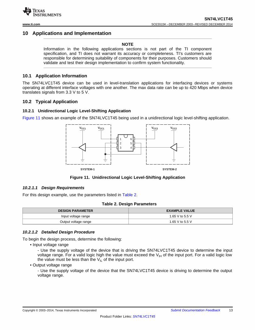
10.2.1 Unidirectional Logic Level-Shifting ApplicationFigure 11 shows an example of the SN74LVC1T45 being used in a unidirectional logic level-shifting application.
Figure 11. Unidirectional Logic Level-Shifting Application
10.2.1.1 Design RequirementsFor this design example, use the parameters listed in Table 2.
Table 2. Design ParametersDESIGN PARAMETER EXAMPLE VALUE
Input voltage range 1.65 V to 5.5 VOutput voltage range 1.65 V to 5.5 V
10.2.1.2 Detailed Design ProcedureTo begin the design process, determine the following:
• Input voltage range- Use the supply voltage of the device that is driving the SN74LVC1T45 device to determine the inputvoltage range. For a valid logic high the value must exceed the VIH of the input port. For a valid logic lowthe value must be less than the VIL of the input port.
• Output voltage range- Use the supply voltage of the device that the SN74LVC1T45 device is driving to determine the outputvoltage range.
Copyright © 2003–2014, Texas Instruments Incorporated Submit Documentation Feedback 13
Product Folder Links: SN74LVC1T45
1
2
3
6
5
4
VCC1 VCC1 VCC2
SYSTEM-1 SYSTEM-2
DIR CTRL
I/O-1
VCC2
I/O-2Pullup/Down
or Bus Hold (1)Pullup/Down
or Bus Hold (1)
SN74LVC1T45SCES515K –DECEMBER 2003–REVISED DECEMBER 2014 www.ti.com
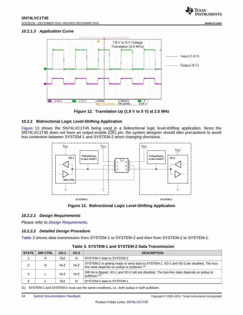
10.2.1.3 Application Curve
Figure 12. Translation Up (1.8 V to 5 V) at 2.5 MHz
10.2.2 Bidirectional Logic Level-Shifting ApplicationFigure 13 shows the SN74LVC1T45 being used in a bidirectional logic level-shifting application. Since theSN74LVC1T45 does not have an output-enable (OE) pin, the system designer should take precautions to avoidbus contention between SYSTEM-1 and SYSTEM-2 when changing directions.
Figure 13. Bidirectional Logic Level-Shifting Application
10.2.2.1 Design RequirementsPlease refer to Design Requirements.
10.2.2.2 Detailed Design ProcedureTable 3 shows data transmission from SYSTEM-1 to SYSTEM-2 and then from SYSTEM-2 to SYSTEM-1.
Table 3. SYSTEM-1 and SYSTEM-2 Data TransmissionSTATE DIR CTRL I/O-1 I/O-2 DESCRIPTION
1 H Out In SYSTEM-1 data to SYSTEM-2SYSTEM-2 is getting ready to send data to SYSTEM-1. I/O-1 and I/O-2 are disabled. The bus-2 H Hi-Z Hi-Z line state depends on pullup or pulldown. (1)
DIR bit is flipped. I/O-1 and I/O-2 still are disabled. The bus-line state depends on pullup or3 L Hi-Z Hi-Z pulldown. (1)
4 L Out In SYSTEM-2 data to SYSTEM-1
(1) SYSTEM-1 and SYSTEM-2 must use the same conditions, i.e., both pullup or both pulldown.
14 Submit Documentation Feedback Copyright © 2003–2014, Texas Instruments Incorporated
Product Folder Links: SN74LVC1T45

SN74LVC1T45www.ti.com SCES515K –DECEMBER 2003–REVISED DECEMBER 2014
10.2.2.2.1 Enable Times
Calculate the enable times for the SN74LVC1T45 using the following formulas:• tPZH (DIR to A) = tPLZ (DIR to B) + tPLH (B to A)• tPZL (DIR to A) = tPHZ (DIR to B) + tPHL (B to A)• tPZH (DIR to B) = tPLZ (DIR to A) + tPLH (A to B)• tPZL (DIR to B) = tPHZ (DIR to A) + tPHL (A to B)
In a bidirectional application, these enable times provide the maximum delay from the time the DIR bit isswitched until an output is expected. For example, if the SN74LVC1T45 initially is transmitting from A to B, thenthe DIR bit is switched; the B port of the device must be disabled before presenting it with an input. After the Bport has been disabled, an input signal applied to it appears on the corresponding A port after the specifiedpropagation delay.
10.2.2.3 Application Curve
Figure 14. Translation Down (5V to 1.8 V) at 2.5 MHz
Copyright © 2003–2014, Texas Instruments Incorporated Submit Documentation Feedback 15
Product Folder Links: SN74LVC1T45
SN74LVC1T45SCES515K –DECEMBER 2003–REVISED DECEMBER 2014 www.ti.com
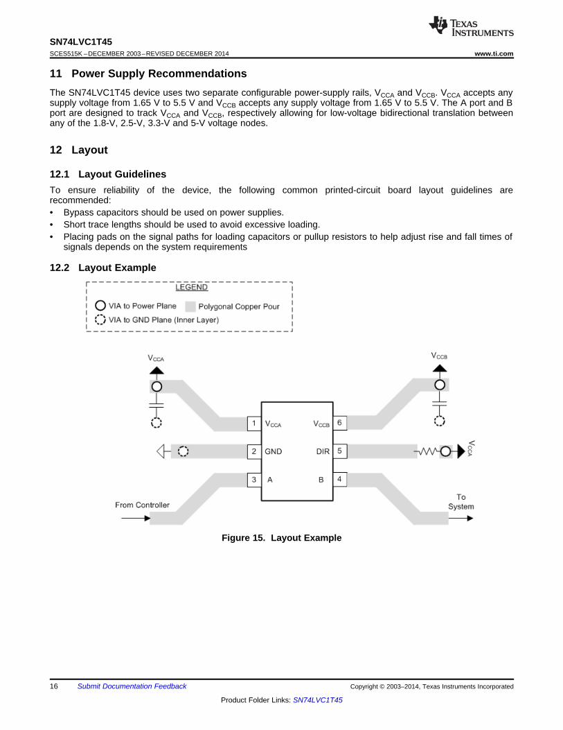
11 Power Supply RecommendationsThe SN74LVC1T45 device uses two separate configurable power-supply rails, VCCA and VCCB. VCCA accepts anysupply voltage from 1.65 V to 5.5 V and VCCB accepts any supply voltage from 1.65 V to 5.5 V. The A port and Bport are designed to track VCCA and VCCB, respectively allowing for low-voltage bidirectional translation betweenany of the 1.8-V, 2.5-V, 3.3-V and 5-V voltage nodes.
12 Layout
12.1 Layout GuidelinesTo ensure reliability of the device, the following common printed-circuit board layout guidelines arerecommended:• Bypass capacitors should be used on power supplies.• Short trace lengths should be used to avoid excessive loading.• Placing pads on the signal paths for loading capacitors or pullup resistors to help adjust rise and fall times of
signals depends on the system requirements
12.2 Layout Example
Figure 15. Layout Example
16 Submit Documentation Feedback Copyright © 2003–2014, Texas Instruments Incorporated
Product Folder Links: SN74LVC1T45

SN74LVC1T45www.ti.com SCES515K –DECEMBER 2003–REVISED DECEMBER 2014
13 Device and Documentation Support
13.1 TrademarksNanoFree is a trademark of Texas Instruments.All other trademarks are the property of their respective owners.
13.2 Electrostatic Discharge CautionThese devices have limited built-in ESD protection. The leads should be shorted together or the device placed in conductive foamduring storage or handling to prevent electrostatic damage to the MOS gates.
13.3 GlossarySLYZ022 — TI Glossary.
This glossary lists and explains terms, acronyms, and definitions.
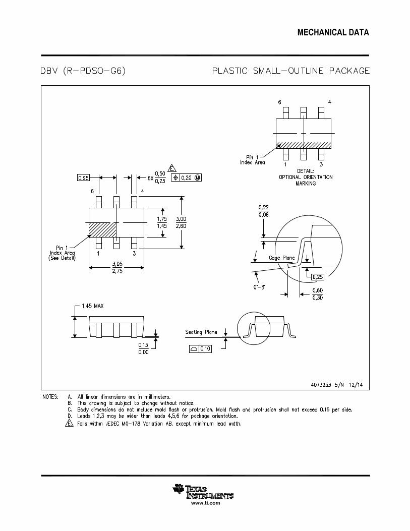
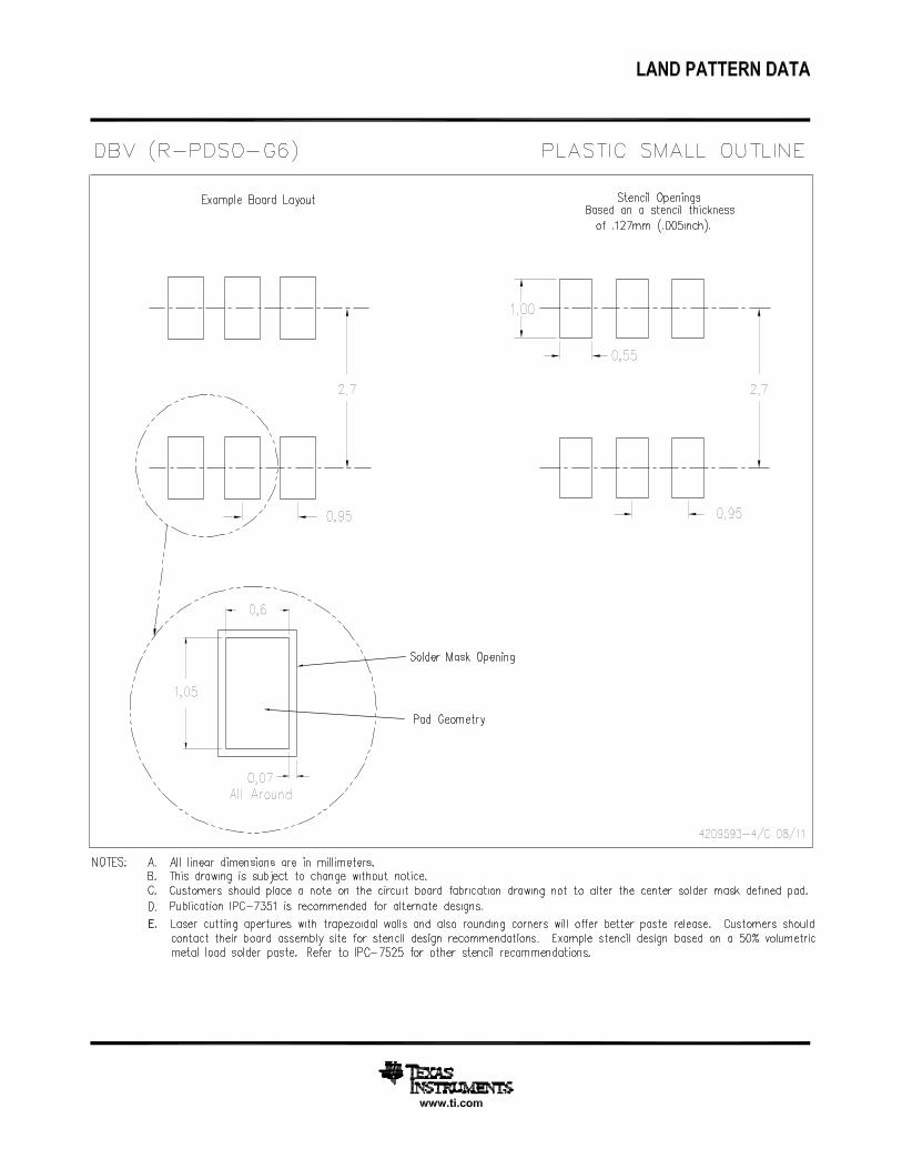
14 Mechanical, Packaging, and Orderable InformationThe following pages include mechanical, packaging, and orderable information. This information is the mostcurrent data available for the designated devices. This data is subject to change without notice and revision ofthis document. For browser-based versions of this data sheet, refer to the left-hand navigation.
Copyright © 2003–2014, Texas Instruments Incorporated Submit Documentation Feedback 17
Product Folder Links: SN74LVC1T45
PACKAGE OPTION ADDENDUM
www.ti.com 21-Jul-2014
Addendum-Page 1
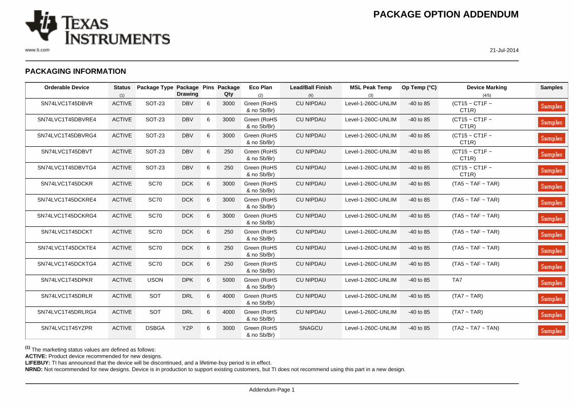
PACKAGING INFORMATION
Orderable Device Status(1)
Package Type PackageDrawing
Pins PackageQty
Eco Plan(2)
Lead/Ball Finish(6)
MSL Peak Temp(3)
Op Temp (°C) Device Marking(4/5)
Samples
SN74LVC1T45DBVR ACTIVE SOT-23 DBV 6 3000 Green (RoHS& no Sb/Br)
CU NIPDAU Level-1-260C-UNLIM -40 to 85 (CT15 ~ CT1F ~ CT1R)
SN74LVC1T45DBVRE4 ACTIVE SOT-23 DBV 6 3000 Green (RoHS& no Sb/Br)
CU NIPDAU Level-1-260C-UNLIM -40 to 85 (CT15 ~ CT1F ~ CT1R)
SN74LVC1T45DBVRG4 ACTIVE SOT-23 DBV 6 3000 Green (RoHS& no Sb/Br)
CU NIPDAU Level-1-260C-UNLIM -40 to 85 (CT15 ~ CT1F ~ CT1R)
SN74LVC1T45DBVT ACTIVE SOT-23 DBV 6 250 Green (RoHS& no Sb/Br)
CU NIPDAU Level-1-260C-UNLIM -40 to 85 (CT15 ~ CT1F ~ CT1R)
SN74LVC1T45DBVTG4 ACTIVE SOT-23 DBV 6 250 Green (RoHS& no Sb/Br)
CU NIPDAU Level-1-260C-UNLIM -40 to 85 (CT15 ~ CT1F ~ CT1R)
SN74LVC1T45DCKR ACTIVE SC70 DCK 6 3000 Green (RoHS& no Sb/Br)
CU NIPDAU Level-1-260C-UNLIM -40 to 85 (TA5 ~ TAF ~ TAR)
SN74LVC1T45DCKRE4 ACTIVE SC70 DCK 6 3000 Green (RoHS& no Sb/Br)
CU NIPDAU Level-1-260C-UNLIM -40 to 85 (TA5 ~ TAF ~ TAR)
SN74LVC1T45DCKRG4 ACTIVE SC70 DCK 6 3000 Green (RoHS& no Sb/Br)
CU NIPDAU Level-1-260C-UNLIM -40 to 85 (TA5 ~ TAF ~ TAR)
SN74LVC1T45DCKT ACTIVE SC70 DCK 6 250 Green (RoHS& no Sb/Br)
CU NIPDAU Level-1-260C-UNLIM -40 to 85 (TA5 ~ TAF ~ TAR)
SN74LVC1T45DCKTE4 ACTIVE SC70 DCK 6 250 Green (RoHS& no Sb/Br)
CU NIPDAU Level-1-260C-UNLIM -40 to 85 (TA5 ~ TAF ~ TAR)
SN74LVC1T45DCKTG4 ACTIVE SC70 DCK 6 250 Green (RoHS& no Sb/Br)
CU NIPDAU Level-1-260C-UNLIM -40 to 85 (TA5 ~ TAF ~ TAR)
SN74LVC1T45DPKR ACTIVE USON DPK 6 5000 Green (RoHS& no Sb/Br)
CU NIPDAU Level-1-260C-UNLIM -40 to 85 TA7
SN74LVC1T45DRLR ACTIVE SOT DRL 6 4000 Green (RoHS& no Sb/Br)
CU NIPDAU Level-1-260C-UNLIM -40 to 85 (TA7 ~ TAR)
SN74LVC1T45DRLRG4 ACTIVE SOT DRL 6 4000 Green (RoHS& no Sb/Br)
CU NIPDAU Level-1-260C-UNLIM -40 to 85 (TA7 ~ TAR)
SN74LVC1T45YZPR ACTIVE DSBGA YZP 6 3000 Green (RoHS& no Sb/Br)
SNAGCU Level-1-260C-UNLIM -40 to 85 (TA2 ~ TA7 ~ TAN)
(1) The marketing status values are defined as follows:ACTIVE: Product device recommended for new designs.LIFEBUY: TI has announced that the device will be discontinued, and a lifetime-buy period is in effect.NRND: Not recommended for new designs. Device is in production to support existing customers, but TI does not recommend using this part in a new design.

PACKAGE OPTION ADDENDUM
www.ti.com 21-Jul-2014
Addendum-Page 2
PREVIEW: Device has been announced but is not in production. Samples may or may not be available.OBSOLETE: TI has discontinued the production of the device.
(2) Eco Plan - The planned eco-friendly classification: Pb-Free (RoHS), Pb-Free (RoHS Exempt), or Green (RoHS & no Sb/Br) - please check http://www.ti.com/productcontent for the latest availabilityinformation and additional product content details.TBD: The Pb-Free/Green conversion plan has not been defined.Pb-Free (RoHS): TI's terms "Lead-Free" or "Pb-Free" mean semiconductor products that are compatible with the current RoHS requirements for all 6 substances, including the requirement thatlead not exceed 0.1% by weight in homogeneous materials. Where designed to be soldered at high temperatures, TI Pb-Free products are suitable for use in specified lead-free processes.Pb-Free (RoHS Exempt): This component has a RoHS exemption for either 1) lead-based flip-chip solder bumps used between the die and package, or 2) lead-based die adhesive used betweenthe die and leadframe. The component is otherwise considered Pb-Free (RoHS compatible) as defined above.Green (RoHS & no Sb/Br): TI defines "Green" to mean Pb-Free (RoHS compatible), and free of Bromine (Br) and Antimony (Sb) based flame retardants (Br or Sb do not exceed 0.1% by weightin homogeneous material)
(3) MSL, Peak Temp. - The Moisture Sensitivity Level rating according to the JEDEC industry standard classifications, and peak solder temperature.
(4) There may be additional marking, which relates to the logo, the lot trace code information, or the environmental category on the device.
(5) Multiple Device Markings will be inside parentheses. Only one Device Marking contained in parentheses and separated by a "~" will appear on a device. If a line is indented then it is a continuationof the previous line and the two combined represent the entire Device Marking for that device.
(6) Lead/Ball Finish - Orderable Devices may have multiple material finish options. Finish options are separated by a vertical ruled line. Lead/Ball Finish values may wrap to two lines if the finishvalue exceeds the maximum column width.
Important Information and Disclaimer:The information provided on this page represents TI's knowledge and belief as of the date that it is provided. TI bases its knowledge and belief on informationprovided by third parties, and makes no representation or warranty as to the accuracy of such information. Efforts are underway to better integrate information from third parties. TI has taken andcontinues to take reasonable steps to provide representative and accurate information but may not have conducted destructive testing or chemical analysis on incoming materials and chemicals.TI and TI suppliers consider certain information to be proprietary, and thus CAS numbers and other limited information may not be available for release.
In no event shall TI's liability arising out of such information exceed the total purchase price of the TI part(s) at issue in this document sold by TI to Customer on an annual basis.
OTHER QUALIFIED VERSIONS OF SN74LVC1T45 :
• Automotive: SN74LVC1T45-Q1
• Enhanced Product: SN74LVC1T45-EP
NOTE: Qualified Version Definitions:
• Automotive - Q100 devices qualified for high-reliability automotive applications targeting zero defects
PACKAGE OPTION ADDENDUM
www.ti.com 21-Jul-2014
Addendum-Page 3
• Enhanced Product - Supports Defense, Aerospace and Medical Applications

TAPE AND REEL INFORMATION
*All dimensions are nominal
Device PackageType
PackageDrawing
Pins SPQ ReelDiameter
(mm)
ReelWidth
W1 (mm)
A0(mm)
B0(mm)
K0(mm)
P1(mm)
W(mm)
Pin1Quadrant
SN74LVC1T45DBVR SOT-23 DBV 6 3000 180.0 8.4 3.23 3.17 1.37 4.0 8.0 Q3
SN74LVC1T45DBVR SOT-23 DBV 6 3000 178.0 9.0 3.23 3.17 1.37 4.0 8.0 Q3
SN74LVC1T45DBVT SOT-23 DBV 6 250 180.0 8.4 3.23 3.17 1.37 4.0 8.0 Q3
SN74LVC1T45DBVT SOT-23 DBV 6 250 178.0 9.0 3.23 3.17 1.37 4.0 8.0 Q3
SN74LVC1T45DCKR SC70 DCK 6 3000 180.0 8.4 2.41 2.41 1.2 4.0 8.0 Q3
SN74LVC1T45DCKR SC70 DCK 6 3000 178.0 9.0 2.4 2.5 1.2 4.0 8.0 Q3
SN74LVC1T45DCKT SC70 DCK 6 250 180.0 8.4 2.41 2.41 1.2 4.0 8.0 Q3
SN74LVC1T45DCKT SC70 DCK 6 250 178.0 9.0 2.4 2.5 1.2 4.0 8.0 Q3
SN74LVC1T45DPKR USON DPK 6 5000 180.0 9.5 1.75 1.75 0.7 4.0 8.0 Q2
SN74LVC1T45DRLR SOT DRL 6 4000 180.0 8.4 1.98 1.78 0.69 4.0 8.0 Q3
SN74LVC1T45DRLR SOT DRL 6 4000 180.0 9.5 1.78 1.78 0.69 4.0 8.0 Q3
SN74LVC1T45YZPR DSBGA YZP 6 3000 178.0 9.2 1.02 1.52 0.63 4.0 8.0 Q1
PACKAGE MATERIALS INFORMATION
www.ti.com 23-Nov-2015
Pack Materials-Page 1

*All dimensions are nominal
Device Package Type Package Drawing Pins SPQ Length (mm) Width (mm) Height (mm)
SN74LVC1T45DBVR SOT-23 DBV 6 3000 202.0 201.0 28.0
SN74LVC1T45DBVR SOT-23 DBV 6 3000 180.0 180.0 18.0
SN74LVC1T45DBVT SOT-23 DBV 6 250 202.0 201.0 28.0
SN74LVC1T45DBVT SOT-23 DBV 6 250 180.0 180.0 18.0
SN74LVC1T45DCKR SC70 DCK 6 3000 202.0 201.0 28.0
SN74LVC1T45DCKR SC70 DCK 6 3000 180.0 180.0 18.0
SN74LVC1T45DCKT SC70 DCK 6 250 202.0 201.0 28.0
SN74LVC1T45DCKT SC70 DCK 6 250 180.0 180.0 18.0
SN74LVC1T45DPKR USON DPK 6 5000 184.0 184.0 19.0
SN74LVC1T45DRLR SOT DRL 6 4000 202.0 201.0 28.0
SN74LVC1T45DRLR SOT DRL 6 4000 184.0 184.0 19.0
SN74LVC1T45YZPR DSBGA YZP 6 3000 220.0 220.0 35.0
PACKAGE MATERIALS INFORMATION
www.ti.com 23-Nov-2015
Pack Materials-Page 2


www.ti.com
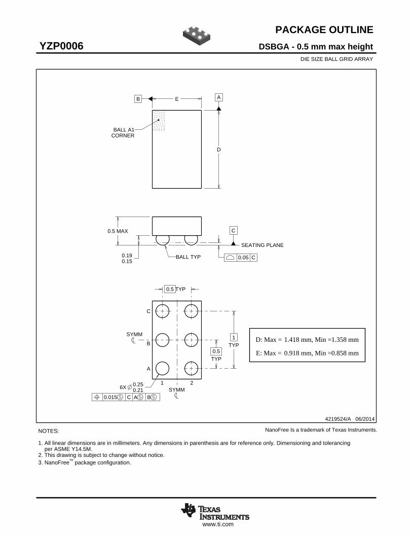
PACKAGE OUTLINE
C0.5 MAX
0.190.15
1TYP
0.5 TYP
6X 0.250.21
0.5TYP
B E A
D
4219524/A 06/2014
DSBGA - 0.5 mm max heightYZP0006DIE SIZE BALL GRID ARRAY
NOTES: 1. All linear dimensions are in millimeters. Any dimensions in parenthesis are for reference only. Dimensioning and tolerancing per ASME Y14.5M.2. This drawing is subject to change without notice.3. NanoFreeTM package configuration.
NanoFree Is a trademark of Texas Instruments.
BALL A1CORNER
SEATING PLANE
BALL TYP 0.05 C
B
A
1 2
0.015 C A B
SYMM
SYMM
C
SCALE 9.000
D: Max =
E: Max =
1.418 mm, Min =
0.918 mm, Min =
1.358 mm
0.858 mm
www.ti.com
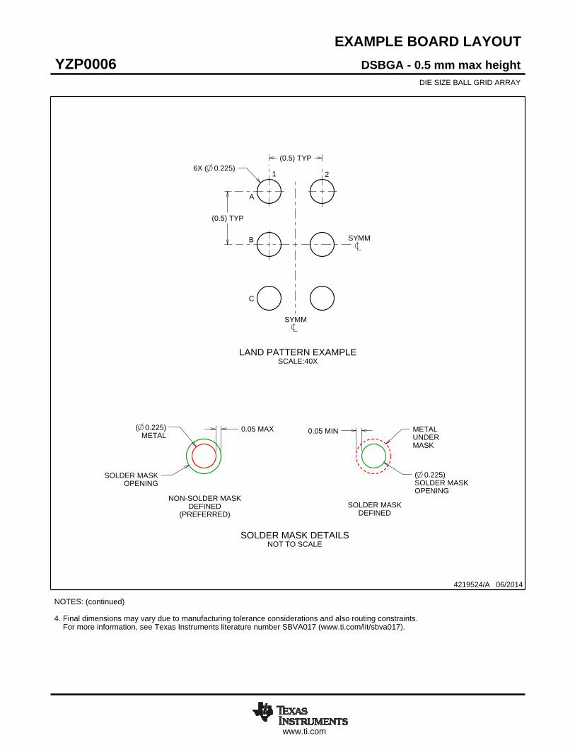
EXAMPLE BOARD LAYOUT
6X ( )0.225(0.5) TYP
(0.5) TYP
( )METAL0.225 0.05 MAX
SOLDER MASKOPENING
METALUNDERMASK
( )SOLDER MASKOPENING
0.225
0.05 MIN
4219524/A 06/2014
DSBGA - 0.5 mm max heightYZP0006DIE SIZE BALL GRID ARRAY
NOTES: (continued) 4. Final dimensions may vary due to manufacturing tolerance considerations and also routing constraints. For more information, see Texas Instruments literature number SBVA017 (www.ti.com/lit/sbva017).
SYMM
SYMM
LAND PATTERN EXAMPLESCALE:40X
1 2
A
B
C
NON-SOLDER MASKDEFINED
(PREFERRED)
SOLDER MASK DETAILSNOT TO SCALE
SOLDER MASKDEFINED

www.ti.com
EXAMPLE STENCIL DESIGN
(0.5)TYP
(0.5) TYP
6X ( 0.25) (R ) TYP0.05
METALTYP
4219524/A 06/2014
DSBGA - 0.5 mm max heightYZP0006DIE SIZE BALL GRID ARRAY
NOTES: (continued) 5. Laser cutting apertures with trapezoidal walls and rounded corners may offer better paste release.
SYMM
SYMM
SOLDER PASTE EXAMPLEBASED ON 0.1 mm THICK STENCIL
SCALE:40X
1 2
A
B
C

IMPORTANT NOTICE
Texas Instruments Incorporated and its subsidiaries (TI) reserve the right to make corrections, enhancements, improvements and otherchanges to its semiconductor products and services per JESD46, latest issue, and to discontinue any product or service per JESD48, latestissue. Buyers should obtain the latest relevant information before placing orders and should verify that such information is current andcomplete. All semiconductor products (also referred to herein as “components”) are sold subject to TI’s terms and conditions of salesupplied at the time of order acknowledgment.TI warrants performance of its components to the specifications applicable at the time of sale, in accordance with the warranty in TI’s termsand conditions of sale of semiconductor products. Testing and other quality control techniques are used to the extent TI deems necessaryto support this warranty. Except where mandated by applicable law, testing of all parameters of each component is not necessarilyperformed.TI assumes no liability for applications assistance or the design of Buyers’ products. Buyers are responsible for their products andapplications using TI components. To minimize the risks associated with Buyers’ products and applications, Buyers should provideadequate design and operating safeguards.TI does not warrant or represent that any license, either express or implied, is granted under any patent right, copyright, mask work right, orother intellectual property right relating to any combination, machine, or process in which TI components or services are used. Informationpublished by TI regarding third-party products or services does not constitute a license to use such products or services or a warranty orendorsement thereof. Use of such information may require a license from a third party under the patents or other intellectual property of thethird party, or a license from TI under the patents or other intellectual property of TI.Reproduction of significant portions of TI information in TI data books or data sheets is permissible only if reproduction is without alterationand is accompanied by all associated warranties, conditions, limitations, and notices. TI is not responsible or liable for such altereddocumentation. Information of third parties may be subject to additional restrictions.Resale of TI components or services with statements different from or beyond the parameters stated by TI for that component or servicevoids all express and any implied warranties for the associated TI component or service and is an unfair and deceptive business practice.TI is not responsible or liable for any such statements.Buyer acknowledges and agrees that it is solely responsible for compliance with all legal, regulatory and safety-related requirementsconcerning its products, and any use of TI components in its applications, notwithstanding any applications-related information or supportthat may be provided by TI. Buyer represents and agrees that it has all the necessary expertise to create and implement safeguards whichanticipate dangerous consequences of failures, monitor failures and their consequences, lessen the likelihood of failures that might causeharm and take appropriate remedial actions. Buyer will fully indemnify TI and its representatives against any damages arising out of the useof any TI components in safety-critical applications.In some cases, TI components may be promoted specifically to facilitate safety-related applications. With such components, TI’s goal is tohelp enable customers to design and create their own end-product solutions that meet applicable functional safety standards andrequirements. Nonetheless, such components are subject to these terms.No TI components are authorized for use in FDA Class III (or similar life-critical medical equipment) unless authorized officers of the partieshave executed a special agreement specifically governing such use.Only those TI components which TI has specifically designated as military grade or “enhanced plastic” are designed and intended for use inmilitary/aerospace applications or environments. Buyer acknowledges and agrees that any military or aerospace use of TI componentswhich have not been so designated is solely at the Buyer's risk, and that Buyer is solely responsible for compliance with all legal andregulatory requirements in connection with such use.TI has specifically designated certain components as meeting ISO/TS16949 requirements, mainly for automotive use. In any case of use ofnon-designated products, TI will not be responsible for any failure to meet ISO/TS16949.
Products ApplicationsAudio www.ti.com/audio Automotive and Transportation www.ti.com/automotiveAmplifiers amplifier.ti.com Communications and Telecom www.ti.com/communicationsData Converters dataconverter.ti.com Computers and Peripherals www.ti.com/computersDLP® Products www.dlp.com Consumer Electronics www.ti.com/consumer-appsDSP dsp.ti.com Energy and Lighting www.ti.com/energyClocks and Timers www.ti.com/clocks Industrial www.ti.com/industrialInterface interface.ti.com Medical www.ti.com/medicalLogic logic.ti.com Security www.ti.com/securityPower Mgmt power.ti.com Space, Avionics and Defense www.ti.com/space-avionics-defenseMicrocontrollers microcontroller.ti.com Video and Imaging www.ti.com/videoRFID www.ti-rfid.comOMAP Applications Processors www.ti.com/omap TI E2E Community e2e.ti.comWireless Connectivity www.ti.com/wirelessconnectivity
Mailing Address: Texas Instruments, Post Office Box 655303, Dallas, Texas 75265Copyright © 2015, Texas Instruments Incorporated
Related Documents