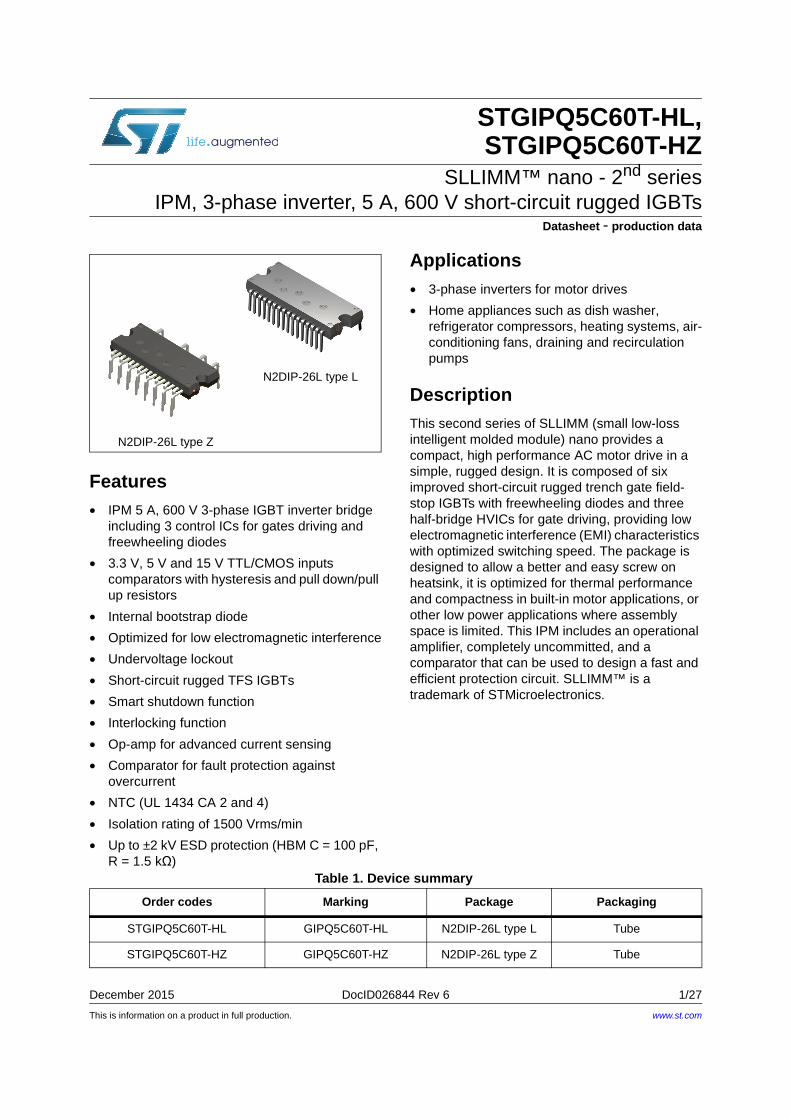
This is information on a product in full production. December 2015 DocID026844 Rev 6 1/27 STGIPQ5C60T-HL, STGIPQ5C60T-HZ SLLIMM™ nano - 2 nd series IPM, 3-phase inverter, 5 A, 600 V short-circuit rugged IGBTs Datasheet - production data Features • IPM 5 A, 600 V 3-phase IGBT inverter bridge including 3 control ICs for gates driving and freewheeling diodes • 3.3 V, 5 V and 15 V TTL/CMOS inputs comparators with hysteresis and pull down/pull up resistors • Internal bootstrap diode • Optimized for low electromagnetic interference • Undervoltage lockout • Short-circuit rugged TFS IGBTs • Smart shutdown function • Interlocking function • Op-amp for advanced current sensing • Comparator for fault protection against overcurrent • NTC (UL 1434 CA 2 and 4) • Isolation rating of 1500 Vrms/min • Up to ±2 kV ESD protection (HBM C = 100 pF, R = 1.5 kΩ) Applications • 3-phase inverters for motor drives • Home appliances such as dish washer, refrigerator compressors, heating systems, air- conditioning fans, draining and recirculation pumps Description This second series of SLLIMM (small low-loss intelligent molded module) nano provides a compact, high performance AC motor drive in a simple, rugged design. It is composed of six improved short-circuit rugged trench gate field- stop IGBTs with freewheeling diodes and three half-bridge HVICs for gate driving, providing low electromagnetic interference (EMI) characteristics with optimized switching speed. The package is designed to allow a better and easy screw on heatsink, it is optimized for thermal performance and compactness in built-in motor applications, or other low power applications where assembly space is limited. This IPM includes an operational amplifier, completely uncommitted, and a comparator that can be used to design a fast and efficient protection circuit. SLLIMM™ is a trademark of STMicroelectronics. N2DIP-26L type Z N2DIP-26L type L Table 1. Device summary Order codes Marking Package Packaging STGIPQ5C60T-HL GIPQ5C60T-HL N2DIP-26L type L Tube STGIPQ5C60T-HZ GIPQ5C60T-HZ N2DIP-26L type Z Tube www.st.com

Welcome message from author
This document is posted to help you gain knowledge. Please leave a comment to let me know what you think about it! Share it to your friends and learn new things together.
Transcript
This is information on a product in full production.
December 2015 DocID026844 Rev 6 1/27
STGIPQ5C60T-HL, STGIPQ5C60T-HZ
SLLIMM™ nano - 2nd series IPM, 3-phase inverter, 5 A, 600 V short-circuit rugged IGBTs
Datasheet - production data
Features• IPM 5 A, 600 V 3-phase IGBT inverter bridge
including 3 control ICs for gates driving and freewheeling diodes
• 3.3 V, 5 V and 15 V TTL/CMOS inputs comparators with hysteresis and pull down/pull up resistors
• Internal bootstrap diode
• Optimized for low electromagnetic interference
• Undervoltage lockout
• Short-circuit rugged TFS IGBTs
• Smart shutdown function
• Interlocking function
• Op-amp for advanced current sensing
• Comparator for fault protection against overcurrent
• NTC (UL 1434 CA 2 and 4)
• Isolation rating of 1500 Vrms/min
• Up to ±2 kV ESD protection (HBM C = 100 pF, R = 1.5 kΩ)
Applications• 3-phase inverters for motor drives
• Home appliances such as dish washer, refrigerator compressors, heating systems, air-conditioning fans, draining and recirculation pumps
DescriptionThis second series of SLLIMM (small low-loss intelligent molded module) nano provides a compact, high performance AC motor drive in a simple, rugged design. It is composed of six improved short-circuit rugged trench gate field-stop IGBTs with freewheeling diodes and three half-bridge HVICs for gate driving, providing low electromagnetic interference (EMI) characteristics with optimized switching speed. The package is designed to allow a better and easy screw on heatsink, it is optimized for thermal performance and compactness in built-in motor applications, or other low power applications where assembly space is limited. This IPM includes an operational amplifier, completely uncommitted, and a comparator that can be used to design a fast and efficient protection circuit. SLLIMM™ is a trademark of STMicroelectronics.
N2DIP-26L type Z
N2DIP-26L type L
Table 1. Device summary
Order codes Marking Package Packaging
STGIPQ5C60T-HL GIPQ5C60T-HL N2DIP-26L type L Tube
STGIPQ5C60T-HZ GIPQ5C60T-HZ N2DIP-26L type Z Tube
www.st.com

Contents STGIPQ5C60T-HL, STGIPQ5C60T-HZ
2/27 DocID026844 Rev 6
Contents
1 Internal schematic and pin description . . . . . . . . . . . . . . . . . . . . . . . . . . 3
2 Absolute maximum ratings . . . . . . . . . . . . . . . . . . . . . . . . . . . . . . . . . . . 5
2.1 Thermal data . . . . . . . . . . . . . . . . . . . . . . . . . . . . . . . . . . . . . . . . . . . . . . . 6
3 Electrical characteristics . . . . . . . . . . . . . . . . . . . . . . . . . . . . . . . . . . . . . 7
3.1 Control part . . . . . . . . . . . . . . . . . . . . . . . . . . . . . . . . . . . . . . . . . . . . . . . . . 9
3.1.1 NTC thermistor . . . . . . . . . . . . . . . . . . . . . . . . . . . . . . . . . . . . . . . . . . . 12
3.2 Waveforms definitions . . . . . . . . . . . . . . . . . . . . . . . . . . . . . . . . . . . . . . . 14
4 Smart shutdown function . . . . . . . . . . . . . . . . . . . . . . . . . . . . . . . . . . . . 15
5 Typical application circuit . . . . . . . . . . . . . . . . . . . . . . . . . . . . . . . . . . . 17
6 Recommendations . . . . . . . . . . . . . . . . . . . . . . . . . . . . . . . . . . . . . . . . . 18
7 Electrical characteristics (curves) . . . . . . . . . . . . . . . . . . . . . . . . . . . . 20
8 Package mechanical data . . . . . . . . . . . . . . . . . . . . . . . . . . . . . . . . . . . . 22
8.1 N2DIP-26L type L package information . . . . . . . . . . . . . . . . . . . . . . . . . . 23
8.2 N2DIP-26L type Z package information . . . . . . . . . . . . . . . . . . . . . . . . . . 24
9 Packaging mechanical data . . . . . . . . . . . . . . . . . . . . . . . . . . . . . . . . . . 25
10 Revision history . . . . . . . . . . . . . . . . . . . . . . . . . . . . . . . . . . . . . . . . . . . 26

DocID026844 Rev 6 3/27
STGIPQ5C60T-HL, STGIPQ5C60T-HZ Internal schematic and pin description
27
1 Internal schematic and pin description
Figure 1. Internal schematic diagram and pin configuration
Internal schematic and pin description STGIPQ5C60T-HL, STGIPQ5C60T-HZ
4/27 DocID026844 Rev 6
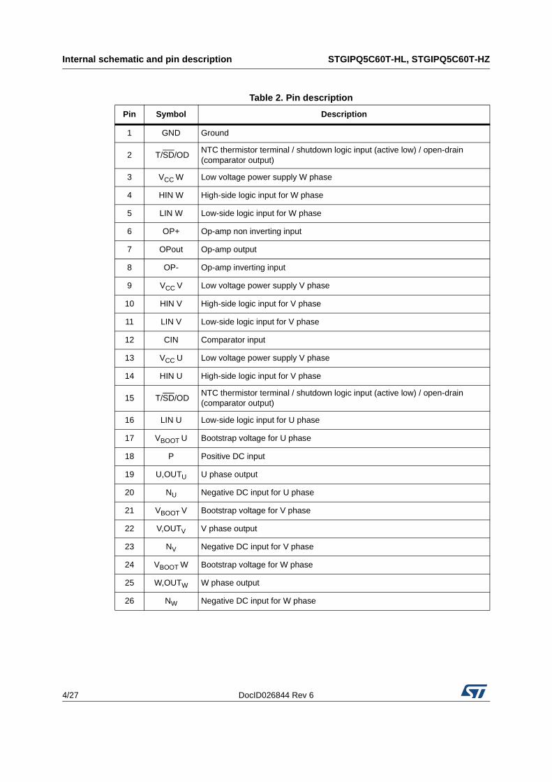
Table 2. Pin description
Pin Symbol Description
1 GND Ground
2 T/SD/ODNTC thermistor terminal / shutdown logic input (active low) / open-drain (comparator output)
3 VCC W Low voltage power supply W phase
4 HIN W High-side logic input for W phase
5 LIN W Low-side logic input for W phase
6 OP+ Op-amp non inverting input
7 OPout Op-amp output
8 OP- Op-amp inverting input
9 VCC V Low voltage power supply V phase
10 HIN V High-side logic input for V phase
11 LIN V Low-side logic input for V phase
12 CIN Comparator input
13 VCC U Low voltage power supply V phase
14 HIN U High-side logic input for V phase
15 T/SD/ODNTC thermistor terminal / shutdown logic input (active low) / open-drain (comparator output)
16 LIN U Low-side logic input for U phase
17 VBOOT U Bootstrap voltage for U phase
18 P Positive DC input
19 U,OUTU U phase output
20 NU Negative DC input for U phase
21 VBOOT V Bootstrap voltage for V phase
22 V,OUTV V phase output
23 NV Negative DC input for V phase
24 VBOOT W Bootstrap voltage for W phase
25 W,OUTW W phase output
26 NW Negative DC input for W phase
DocID026844 Rev 6 5/27
STGIPQ5C60T-HL, STGIPQ5C60T-HZ Absolute maximum ratings
27
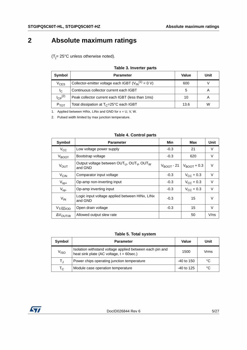
2 Absolute maximum ratings
(Tj= 25°C unless otherwise noted).
Table 3. Inverter parts
Symbol Parameter Value Unit
VCES Collector-emitter voltage each IGBT (VIN(1) = 0 V)
1. Applied between HINx, LINx and GND for x = U, V, W.
600 V
IC Continuous collector current each IGBT 5 A
ICP(2)
2. Pulsed width limited by max junction temperature.
Peak collector current each IGBT (less than 1ms) 10 A
PTOT Total dissipation at TC=25°C each IGBT 13.6 W
Table 4. Control parts
Symbol Parameter Min Max Unit
VCC Low voltage power supply -0.3 21 V
VBOOT Bootstrap voltage -0.3 620 V
VOUTOutput voltage between OUTU, OUTV, OUTW and GND
VBOOT - 21 VBOOT + 0.3 V
VCIN Comparator input voltage -0.3 VCC + 0.3 V
Vop+ Op-amp non-inverting input -0.3 VCC + 0.3 V
Vop- Op-amp inverting input -0.3 VCC + 0.3 V
VINLogic input voltage applied between HINx, LINx and GND
-0.3 15 V
VT/SD/OD Open drain voltage -0.3 15 V
∆VOUT/dt Allowed output slew rate 50 V/ns
Table 5. Total system
Symbol Parameter Value Unit
VISOIsolation withstand voltage applied between each pin and heat sink plate (AC voltage, t = 60sec.)
1500 Vrms
TJ Power chips operating junction temperature -40 to 150 °C
TC Module case operation temperature -40 to 125 °C

Absolute maximum ratings STGIPQ5C60T-HL, STGIPQ5C60T-HZ
6/27 DocID026844 Rev 6
2.1 Thermal data
Table 6. Thermal data
Symbol Parameter Value Unit
Rth(j-c)Thermal resistance junction-case single IGBT 9.2
°C/WThermal resistance junction-case single diode 15
DocID026844 Rev 6 7/27
STGIPQ5C60T-HL, STGIPQ5C60T-HZ Electrical characteristics
27
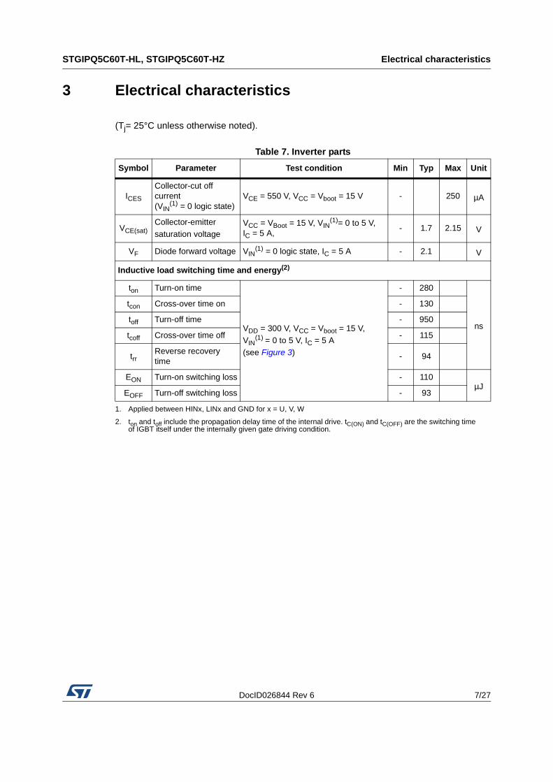
3 Electrical characteristics
(Tj= 25°C unless otherwise noted).
Table 7. Inverter parts
Symbol Parameter Test condition Min Typ Max Unit
ICES
Collector-cut off current (VIN
(1) = 0 logic state)
1. Applied between HINx, LINx and GND for x = U, V, W
VCE = 550 V, VCC = Vboot = 15 V - 250 µA
VCE(sat)Collector-emittersaturation voltage
VCC = VBoot = 15 V, VIN(1)= 0 to 5 V,
IC = 5 A, - 1.7 2.15 V
VF Diode forward voltage VIN(1) = 0 logic state, IC = 5 A - 2.1 V
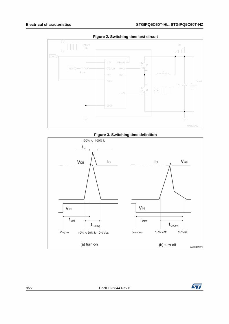
Inductive load switching time and energy(2)
2. ton and toff include the propagation delay time of the internal drive. tC(ON) and tC(OFF) are the switching time of IGBT itself under the internally given gate driving condition.
ton Turn-on time
VDD = 300 V, VCC = Vboot = 15 V, VIN
(1) = 0 to 5 V, IC = 5 A(see Figure 3)
- 280
ns
tcon Cross-over time on - 130
toff Turn-off time - 950
tcoff Cross-over time off - 115
trrReverse recovery time
- 94
EON Turn-on switching loss - 110µJ
EOFF Turn-off switching loss - 93
Electrical characteristics STGIPQ5C60T-HL, STGIPQ5C60T-HZ
8/27 DocID026844 Rev 6
Figure 2. Switching time test circuit
Figure 3. Switching time definition
VCE IC IC
VIN
t ON
t C(ON)
VIN(ON) 10% IC 90% IC 10% VCE
(a) turn-on (b) turn-off
t rr
100% IC 100% IC
VIN
VCE
t OFFt C(OFF)
VIN(OFF) 10% VCE 10% IC
AM09223V1
DocID026844 Rev 6 9/27
STGIPQ5C60T-HL, STGIPQ5C60T-HZ Electrical characteristics
27
3.1 Control part(VCC=15 V unless otherwise specified)
Table 8. Low voltage power supply
Symbol Parameter Test condition Min Typ Max Unit
VCC_hys VCC UV hysteresis 1.2 1.5 1.8 V
VCCH_th(on) VCCH UV turn-on threshold 11.5 12 12.5 V
VCCH_th(off) VCCH UV turn-off threshold 10 10.5 11 V
IqccuUnder voltage quiescent supply current
VCC=10V; T/SD/OD=5V; LIN=HIN=CIN=0V
150 µA
Iqcc Quiescent current VCC=10 V; T/SD/OD=5V; LIN=HIN=CIN=0V
1 mA
VREFInternal comparator (CIN) reference voltage
0.51 0.54 0.60 V
Table 9. Bootstrapped voltage
Symbol Parameter Test condition Min Typ Max Unit
VBS_hys VBS UV hysteresis 1.2 1.5 1.8 V
VBS_th(on) VBS UV turn-on threshold 11.1 11.5 12.1 V
VBS_th(off) VBS UV turn-off threshold 9.8 10 10.6 V
IQBSUUndervoltage VBS quiescent current
VBS <9V T/SD/OD=5V; LIN=0V;HIN=5V;CIN=0V;
70 110 µA
IQBS VBS quiescent current VBS =15V T/SD/OD=5V; LIN=0V;HIN=5V;CIN=0V;
150 210 µA
RDS(on)Bootstrap driver on resistance
LVG ON 120 Ω

Electrical characteristics STGIPQ5C60T-HL, STGIPQ5C60T-HZ
10/27 DocID026844 Rev 6
Table 10. Logic inputs
Symbol Parameter Test condition Min Typ Max Unit
Vil Low logic level voltage 0.8 V
Vih High logic level voltage 2.25 V
IHINh HIN logic “1” input bias HIN=15V 20 40 100 µA
IHINlHIN logic “0” input bias current
HIN=0V 1 µA
ILINhLIN logic “1” input bias current
LIN=15V 20 40 100 µA
ILINlLIN logic “0” input bias current
LIN=0V 1 µA
ISDhSD logic “0” input bias current
SD =15V 220 295 370 µA
ISDlSD logic “1” input bias current
SD =0V 3 µA
Dt Dead time See Figure 8 180 ns
Table 11. Op-amp characteristics
Symbol Parameter Test condition Min Typ Max Unit
Vio Input offset voltage Vic=0V, Vo=7.5V 6 mV
Iio Input offset current Vic=0V, Vo=7.5V 4 40 nA
Iib Input bias current(1) Vic=0V, Vo=7.5V 100 200 nA
VicmInput common mode voltage range
0 V
VOLLow level output voltage range
RL=10 kΩ to VCC 75 150 mV
VOHHigh level output voltage range
RL=10 kΩ to GND 14 14.7 V
Io Output short-circuit current
Source
Vid=+1V, Vo=0V16 30 mA
Sink
Vid=-1V, Vo= VCC50 80 mA
SR Slew rateVi=1-4V; CL=100pF; unity gain
2.5 3.8 V/µs
GBWP Gain bandwidth product Vo=7.5V 8 12 MHz
Avd Large signal voltage gain RL=2 kΩ 70 85 dB
DocID026844 Rev 6 11/27
STGIPQ5C60T-HL, STGIPQ5C60T-HZ Electrical characteristics
27
SVRSupply voltage rejection ratio
vs. Vcc 60 75 dB
CMRRCommon mode rejection ratio
55 70 dB
1. The direction of the input current is out of the IC.
Table 12. Sense comparator characteristics
Symbol Parameter Test condition Min Typ Max Unit
Iib Input bias current VCin=1V - 3 µA
VodOpen drain low level output voltage
Iod=3mA - 0.5 V
RON_ODOpen drain low level output resistance
Iod=3mA - 166 Ω
RPD_SD SD pull down resistor(1)
1. Equivalent value as a result of the resistances of three drivers in parallel
- 125 kΩ
td_comp Comparator delayT/SD/OD pulled to 5V through 100 kΩ resistor
- 90 130 ns
SR Slew rate CL=180pF; Rpu=5 kΩ - 60 V/µs
tsdShutdown to high/low side driver propagation delay
VOUT =0V, Vboot = VCC, VIN=0 to 3.3V
- 125 ns
tisd
Comparator triggering to high/low side driver turn-off propagation delay
Measured applying a voltage step from 0V to 3.3V to pin of CIN
- 200 ns
Table 13. Truth table
ConditionLogic input (Vl) Output
T/SD/OD LIN HIN LVG HVG
Shutdown enable half-bridge tri-state L X(1)
1. X = don’t care
X(1) L L
Interlocking half-bridge tri-state H H H L L
0 “logic state”half-bridge tri-state
H L L L L
1 “logic state”Low side direct driving
H H L H L
1 “logic state” high side direct driving
H L H L H
Table 11. Op-amp characteristics (continued)
Symbol Parameter Test condition Min Typ Max Unit
Electrical characteristics STGIPQ5C60T-HL, STGIPQ5C60T-HZ
12/27 DocID026844 Rev 6
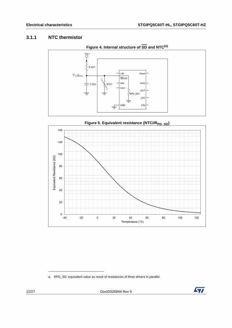
3.1.1 NTC thermistor
Figure 4. Internal structure of SD and NTC(a)
Figure 5. Equivalent resistance (NTC//RPD_SD)
a. RPD_SD: equivalent value as result of resistances of three drivers in parallel.
DocID026844 Rev 6 13/27
STGIPQ5C60T-HL, STGIPQ5C60T-HZ Electrical characteristics
27
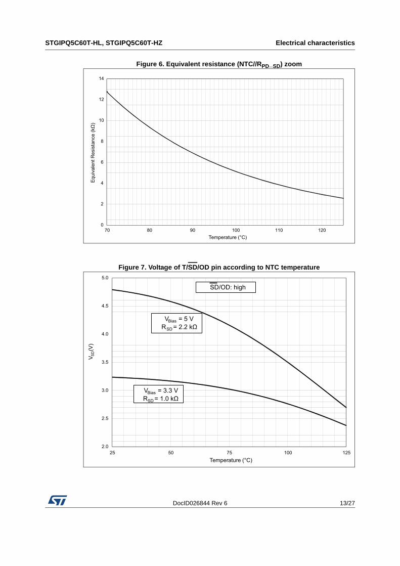
Figure 6. Equivalent resistance (NTC//RPD_SD) zoom
Figure 7. Voltage of T/SD/OD pin according to NTC temperature
Electrical characteristics STGIPQ5C60T-HL, STGIPQ5C60T-HZ
14/27 DocID026844 Rev 6
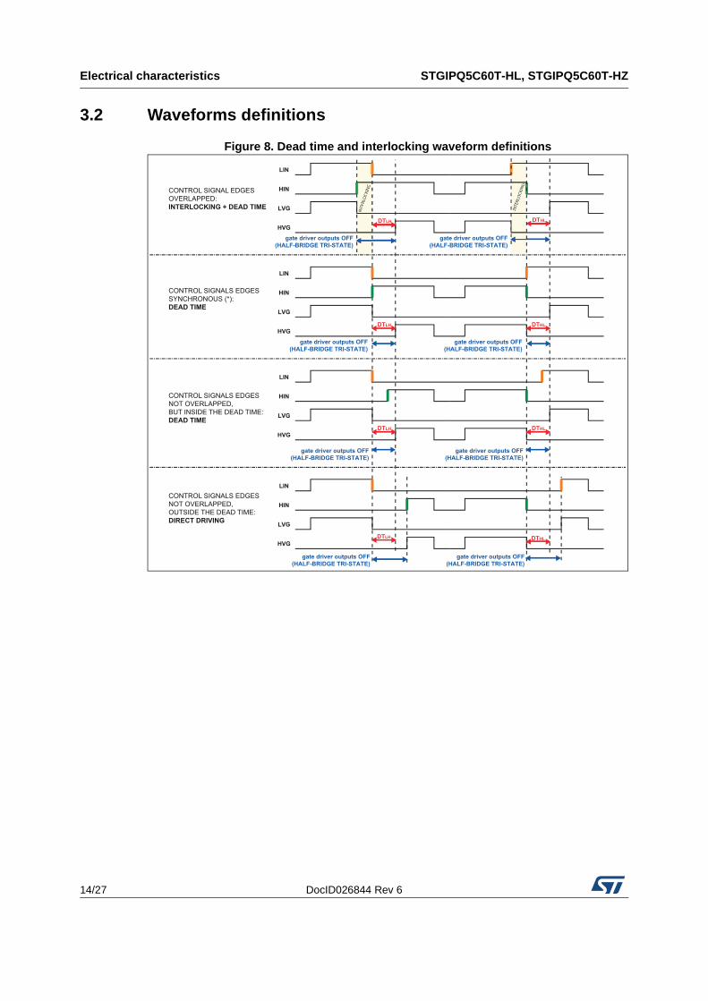
3.2 Waveforms definitions
Figure 8. Dead time and interlocking waveform definitions
INTE
RLO
CKI
NG
INTE
RLO
CKI
NG
INTE
RLO
CKI
NG
INTE
RLO
CKI
NGG
DocID026844 Rev 6 15/27
STGIPQ5C60T-HL, STGIPQ5C60T-HZ Smart shutdown function
27
4 Smart shutdown function
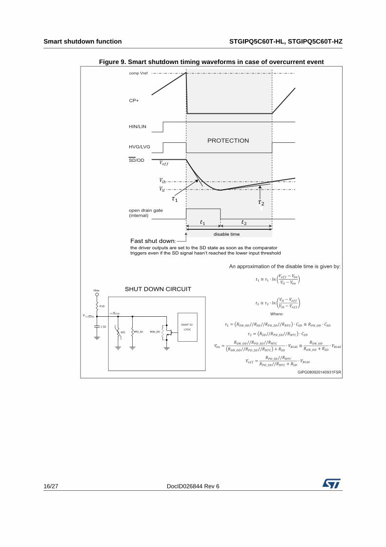
The device integrates a comparator for fault sensing purposes. The comparator has an internal voltage reference VREF connected to the inverting input, while the non-inverting input on pin (CIN) can be connected to an external shunt resistor for simple overcurrent protection.
When the comparator triggers, the device is set to the Shutdown state and both its outputs are switched to the low-level setting, causing the half bridge to enter a tri-state.
In common overcurrent protection architectures, the comparator output is usually connected to the Shutdown input through an RC network that provides a mono-stable circuit which implements a protection time following a fault condition.
Our smart shutdown architecture immediately turns off the output gate driver in case of overcurrent along a preferential path for the fault signal which directly switches off the outputs. The time delay between the fault and output shutdown no longer depends on the RC values of the external network connected to the shutdown pin. At the same time, the DMOS connected to the open-drain output (pin T/SD/OD) is turned on by the internal logic, which holds it on until the shutdown voltage is lower than the logic input lower threshold (Vil).
Also, the smart shutdown function allows increasing the real disable time without increasing the constant time of the external RC network.
An NTC thermistor for temperature monitoring is internally connected in parallel to the SD pin. To avoid undesired shutdown, keep the voltage VT/SD/OD higher than the high-level logic threshold by setting the pull-up resistor RSD to 1 kΩ or 2.2 kΩ for the 3.3 V or 5 V MCU power supplies, respectively.
Smart shutdown function STGIPQ5C60T-HL, STGIPQ5C60T-HZ
16/27 DocID026844 Rev 6
Figure 9. Smart shutdown timing waveforms in case of overcurrent event
SHUT DOWN CIRCUIT
An approximation of the disable time is given by:
HIN/LIN
HVG/LVG
open drain gate(internal)
comp Vref
CP+
PROTECTION
Fast shut down:the driver outputs are set to the SD state as soon as the comparatortriggers even if the SD signal hasn’t reached the lower input threshold
disable time
SD/OD
GIPG080920140931FSR
T1/SD/ODV
SMART SD
LOGIC
T1/SD/OD
RPD_SD
C SD
R SD
Vbias
NTC RON_OD
DocID026844 Rev 6 17/27
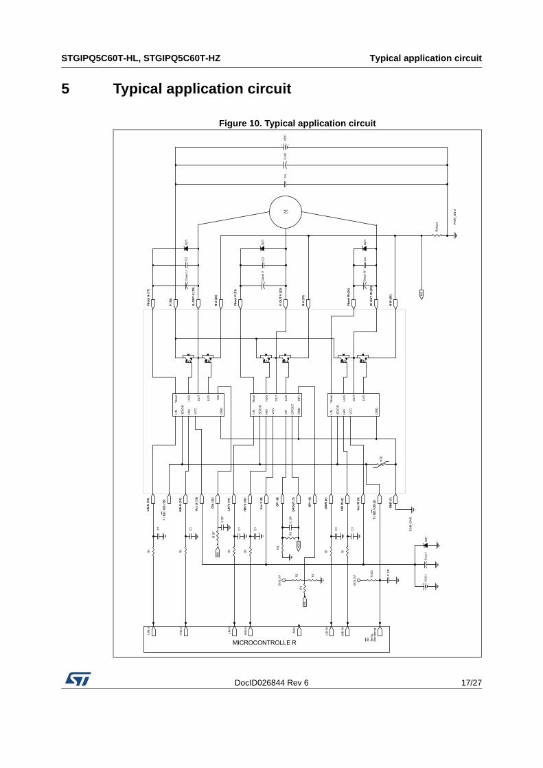
STGIPQ5C60T-HL, STGIPQ5C60T-HZ Typical application circuit
27
5 Typical application circuit
Figure 10. Typical application circuit
Recommendations STGIPQ5C60T-HL, STGIPQ5C60T-HZ
18/27 DocID026844 Rev 6
6 Recommendations
• HIN and LIN are active-high logic input signals, each having an integrated 500 kΩ (typ.) pull-down resistor. Wire each input as short as possible and use RC filters (R1, C1) on each to prevent input signal oscillation. The filters should have a time constant of approximately 100 ns and must be placed as close as possible to the IPM input pins.
• Use a bypass capacitor Cvcc (aluminum or tantalum) to reduce the transient circuit demand on the power supply and a decoupling capacitor C2 (from 100 to 220 nF, ceramic with low ESR), placed as close as possible to each Vcc pin and in parallel to the bypass capacitor, to reduce high frequency switching noise distributed on the power supply lines.
• To prevent circuit malfunction, place an RC filter (RSF, CSF) with a time constant (RSF x CSF) of 1µs as close as possible to the CIN pin.
• The SD is an input/output pin (open drain type if used as output). An integrated NTC thermistor is connected internally between the SD pin and GND. The pull-up resistor RSD causes the voltage VSD-GND to decrease as the temperature increases. To always maintain the voltage above the high-level logic threshold, use a 1 kΩ or 2.2 kΩ pull-up resistor for a 3.3 V or 5 V MCU power supply, respectively. Size the filter on SD appropriately to obtain the desired re-start time after a fault event, and locate it as close as possible to the SD pin.
• Filter high-frequency disturbances by placing the decoupling capacitor C3 (from 100 to 220 nF, ceramic with low ESR) in parallel with each Cboot.
• Prevent overvoltage with Zener diodes DZ1 between the VCC pins and GND and in parallel with each Cboot.
• Locate the decoupling capacitor C4 (from 100 to 220 nF, ceramic with low ESR) in parallel with the electrolytic capacitor Cvdc to prevent surge destruction. Place capacitors C4 (especially) and Cvdc as close as possible to the IPM.
• By integrating an application-specific type HVIC inside the module, direct coupling to the MCU terminals without an opto-coupler is possible.
• Use low inductance shunt resistors for phase leg current sensing.
• The wiring between N pins, the shunt resistor and PWR_GND should be as short as possible.
• Connect SGN_GND to PWR_GND at only one point (near the shunt resistor terminal), to avoid any malfunction due to power ground fluctuation.
Table 14. Recommended operating conditions
Symbol Parameter Test condition Min. Typ. Max. Unit
VPN Supply voltageApplied between P-Nu,Nv,Nw
300 500 V
VCC Control supply voltage Applied between Vcc-GND 13.5 15 18 V
VBS High side bias voltageApplied between Vbootx-OUT for x=U,V,W
13 18 V
tdeadBlanking time to prevent Arm-short
For each input signal 1.5 µs
DocID026844 Rev 6 19/27
STGIPQ5C60T-HL, STGIPQ5C60T-HZ Recommendations
27
fPWM PWM input signal-40°C<Tc<100°C-40°C<Tj<125°C
25 kHz
Tc Case operation temperature 100 °C
Table 14. Recommended operating conditions (continued)
Symbol Parameter Test condition Min. Typ. Max. Unit
Electrical characteristics (curves) STGIPQ5C60T-HL, STGIPQ5C60T-HZ
20/27 DocID026844 Rev 6
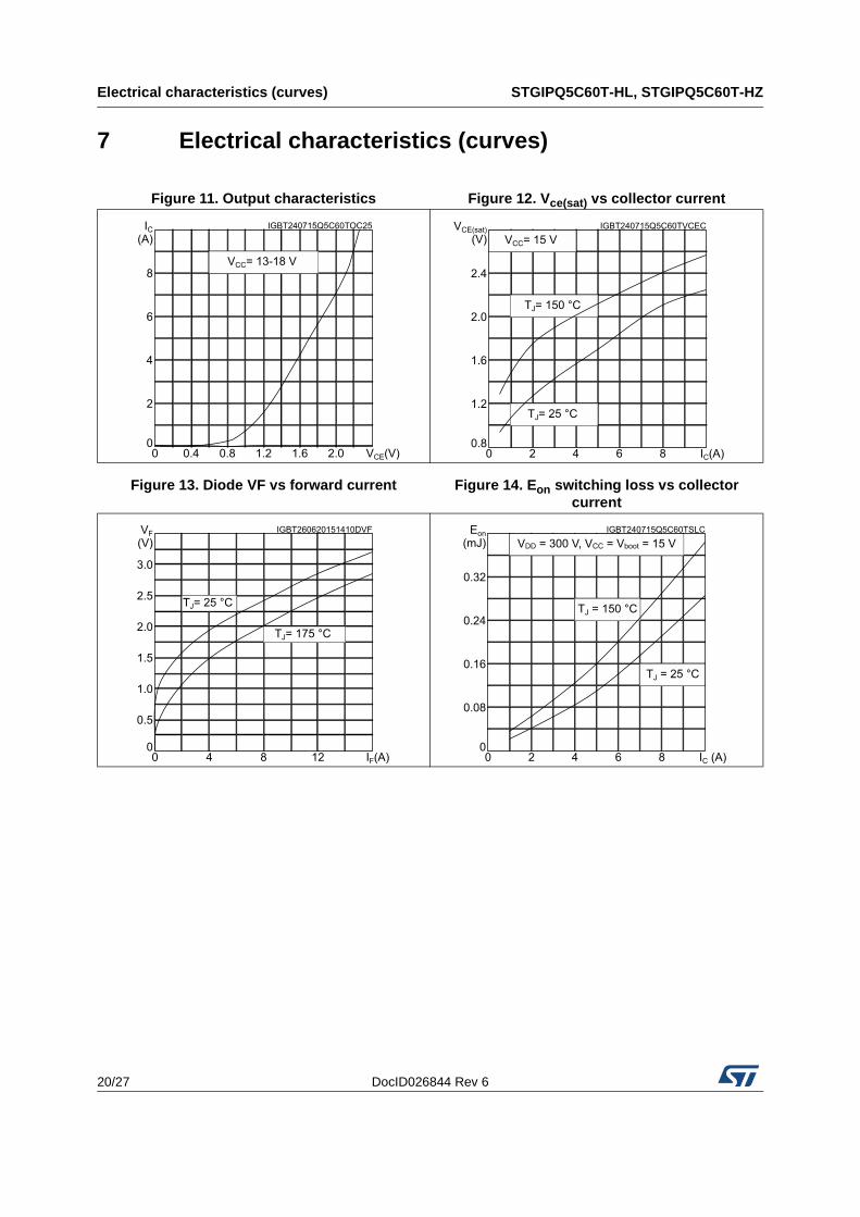
7 Electrical characteristics (curves)
Figure 11. Output characteristics Figure 12. Vce(sat) vs collector current
Figure 13. Diode VF vs forward current Figure 14. Eon switching loss vs collector current
DocID026844 Rev 6 21/27
STGIPQ5C60T-HL, STGIPQ5C60T-HZ Electrical characteristics (curves)
27
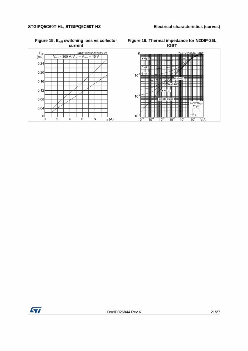
Figure 15. Eoff switching loss vs collector current
Figure 16. Thermal impedance for N2DIP-26L IGBT

Package mechanical data STGIPQ5C60T-HL, STGIPQ5C60T-HZ
22/27 DocID026844 Rev 6
8 Package mechanical data
In order to meet environmental requirements, ST offers these devices in different grades of ECOPACK® packages, depending on their level of environmental compliance. ECOPACK® specifications, grade definitions and product status are available at: www.st.com. ECOPACK® is an ST trademark.
DocID026844 Rev 6 23/27
STGIPQ5C60T-HL, STGIPQ5C60T-HZ Package mechanical data
27
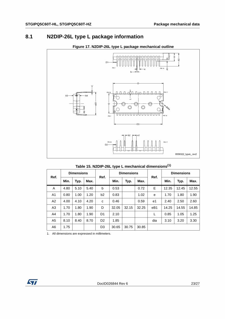
8.1 N2DIP-26L type L package information
Figure 17. N2DIP-26L type L package mechanical outline
Table 15. N2DIP-26L type L mechanical dimensions(1)
1. All dimensions are expressed in millimeters.
Ref.Dimensions
Ref.Dimensions
Ref.Dimensions
Min. Typ. Max. Min. Typ. Max. Min. Typ. Max.
A 4.80 5.10 5.40 b 0.53 0.72 E 12.35 12.45 12.55
A1 0.80 1.00 1.20 b2 0.83 1.02 e 1.70 1.80 1.90
A2 4.00 4.10 4.20 c 0.46 0.59 e1 2.40 2.50 2.60
A3 1.70 1.80 1.90 D 32.05 32.15 32.25 eB1 14.25 14.55 14.85
A4 1.70 1.80 1.90 D1 2.10 L 0.85 1.05 1.25
A5 8.10 8.40 8.70 D2 1.85 dia 3.10 3.20 3.30
A6 1.75 D3 30.65 30.75 30.85

Package mechanical data STGIPQ5C60T-HL, STGIPQ5C60T-HZ
24/27 DocID026844 Rev 6
8.2 N2DIP-26L type Z package information
Figure 18. N2DIP-26L type Z package mechanical outline
Table 16. N2DIP-26L type Z mechanical dimensions(1)
1. All dimensions are expressed in millimeters.
Ref.Dimensions
Ref.Dimensions
Ref.Dimensions
Min. Typ. Max. Min. Typ. Max. Min. Typ. Max.
A 4.80 5.10 5.40 b 0.53 0.72 E 12.35 12.45 12.55
A1 0.80 1.00 1.20 b2 0.83 1.02 e 1.70 1.80 1.90
A2 4.00 4.10 4.20 c 0.46 0.59 e1 2.40 2.50 2.60
A3 1.70 1.80 1.90 D 32.05 32.15 32.25 eB1 16.10 16.40 16.70
A4 1.70 1.80 1.90 D1 2.10 eB2 21.18 21.48 21.78
A5 8.10 8.40 8.70 D2 1.85 L 0.85 1.05 1.25
A6 1.75 D3 30.65 30.75 30.85 dia 3.10 3.20 3.30

DocID026844 Rev 6 25/27
STGIPQ5C60T-HL, STGIPQ5C60T-HZ Packaging mechanical data
27
9 Packaging mechanical data
Figure 19. N2DIP-26L tube dimensions(b)
b. All dimensions are expressed in millimeters.
Revision history STGIPQ5C60T-HL, STGIPQ5C60T-HZ
26/27 DocID026844 Rev 6
10 Revision history
Table 17. Document revision history
Date Revision Changes
08-Sep-2014 1 Initial release.
29-Oct-2014 2
– Minor text edits throughout the document.– Updated Figure 1, 4, 7, 9 and 10.– Added Figure 6 and Figure 7.
– Updated values for the ISDh and ISDl parameters in Table 10: Logic inputs.
– Added footnote to Table 12.– Removed NTC thermistor table and “Resistance variation vs.
temperature” equation from Section 3.1.1: NTC thermistor
07-Nov-2014 3 Minor text and formatting edits throughout document.
24-Jul-2015 4
Minor text and formatting edits throughout document.Updated cover page package image.
Updated Table 3, Table 6, Table 7, Table 8, Table 9, and Table 10
Added Section 7: Electrical characteristics (curves)
21-Aug-2015 5Modified: Figure 13
Minor text changes
09-Dec-2015 6Modified: Features
Minor text changes
DocID026844 Rev 6 27/27
STGIPQ5C60T-HL, STGIPQ5C60T-HZ
27
IMPORTANT NOTICE – PLEASE READ CAREFULLY
STMicroelectronics NV and its subsidiaries (“ST”) reserve the right to make changes, corrections, enhancements, modifications, and improvements to ST products and/or to this document at any time without notice. Purchasers should obtain the latest relevant information on ST products before placing orders. ST products are sold pursuant to ST’s terms and conditions of sale in place at the time of order acknowledgement.
Purchasers are solely responsible for the choice, selection, and use of ST products and ST assumes no liability for application assistance or the design of Purchasers’ products.
No license, express or implied, to any intellectual property right is granted by ST herein.
Resale of ST products with provisions different from the information set forth herein shall void any warranty granted by ST for such product.
ST and the ST logo are trademarks of ST. All other product or service names are the property of their respective owners.
Information in this document supersedes and replaces information previously supplied in any prior versions of this document.
© 2015 STMicroelectronics – All rights reserved
Related Documents


