SJTU Zhou Lingling 1 Chapter 5 Differential and Multistage Amplifier

SJTU Zhou Lingling1 Chapter 5 Differential and Multistage Amplifier.
Dec 22, 2015
Welcome message from author
This document is posted to help you gain knowledge. Please leave a comment to let me know what you think about it! Share it to your friends and learn new things together.
Transcript

SJTU Zhou Lingling 1
Chapter 5
Differential and Multistage Amplifier

SJTU Zhou Lingling 2
Outline
• Introduction• The CMOS Differential Pair• Small-Signal Operation of the MOS Differential
Pair• The BJT Differential Pair• The differential Amplifier with Active Load• Frequency Response of the Differential amplifier• Multistage Amplifiers

SJTU Zhou Lingling 3
Introduction
• Two reasons of the differential amplifier suited for IC fabrication: IC fabrication is capable of providing matched devices.Utilizing more components than single-ended
amplifier:Differential circuits are much less sensitive to noise and
interference.Differential configuration enable us to bias the amplifier and
to couple amplifier stages without the need for bypass and coupling capacitors.

SJTU Zhou Lingling 4
The MOS Differential Pair
• Basic structure of differential pair.
• Characteristics

SJTU Zhou Lingling 5
The MOS Differential Pair
SJTU Zhou Lingling 6
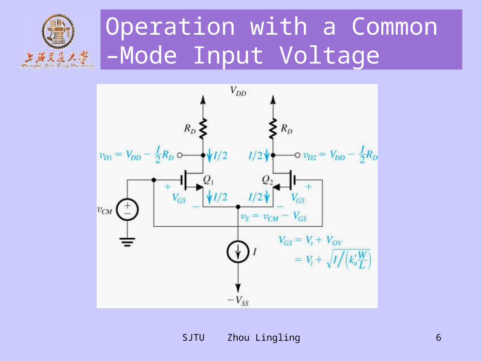
Operation with a Common –Mode Input Voltage

SJTU Zhou Lingling 7
Operation with a Common –Mode Input Voltage
• Symmetry circuit.
• Common-mode voltage.
• Current I divides equally between two transistors.
• The difference between two drains is zero.
• The differential pair rejects the common-mode input signals.

SJTU Zhou Lingling 8
Operation with a Differential Input Voltage
The MOS differential pair with a differential input signal vid applied.
With vid positive: vGS1 vGS2, iD1 iD2, and vD1 vD2; thus (vD2 vD1) will be positive.
With vid negative: vGS1 vGS2, iD1 iD2, and vD1 vD2; thus (vD2 vD1) will be negative.

SJTU Zhou Lingling 9
Operation with a Differential Input Voltage
• Differential input voltage.• Response to the differential input signal.• The current I can be steered from one transistor to
the other by varying the differential input voltage in the range:
• When differential input voltage is very small, the differential output voltage is proportional to it, and the gain is high.
OVidOV VvV 22

SJTU Zhou Lingling 10
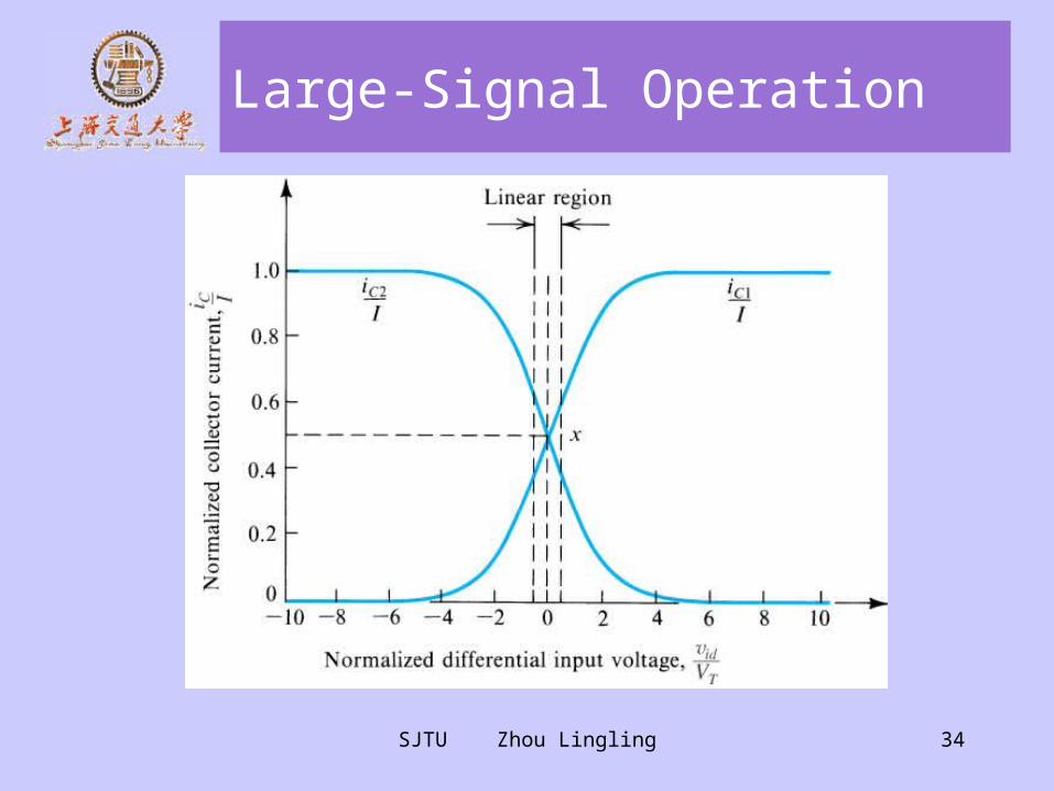
Large-Signal Operation
Transfer characteristic curves
Normalized plots of the currents in a MOSFET differential pair.
Note that VOV is the overdrive voltage at which Q1 and Q2 operate when conducting drain currents equal to I/2.

SJTU Zhou Lingling 11
Large-Signal Operation
• Nonlinear curves.• Maximum value of input differential voltage.
• When vid = 0, two drain currents are equal to I/2.
• Linear segment.• Linearity can be increased by increasing overdrive
voltage(see next slide).• Price paid is a reduction in gain(current I is kept
constant).

SJTU Zhou Lingling 12
Large-Signal Operation
The linear range of operation of the MOS differential pair can be extended by operating the transistor at a higher value of VOV.

SJTU Zhou Lingling 13
Small-Signal Operation of MOS Differential Pair
• Linear amplifier
• Differential gain
• Common-mode gain
• Common-mode rejection ratio(CMRR)
• Mismatch on CMRR
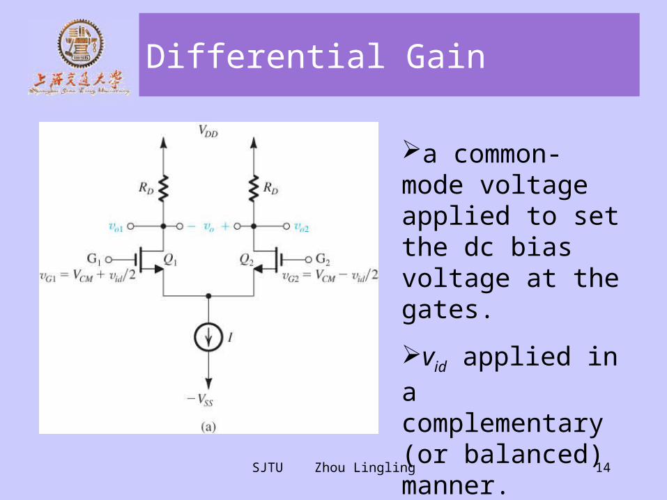
SJTU Zhou Lingling 14
Differential Gain
a common-mode voltage applied to set the dc bias voltage at the gates.
vid applied in a complementary (or balanced) manner.

SJTU Zhou Lingling 15
Differential Gain
Signal voltage at the joint source connection must be zero.

SJTU Zhou Lingling 16
Differential Gain
An alternative way of looking at the small-signal operation of the circuit.
SJTU Zhou Lingling 17
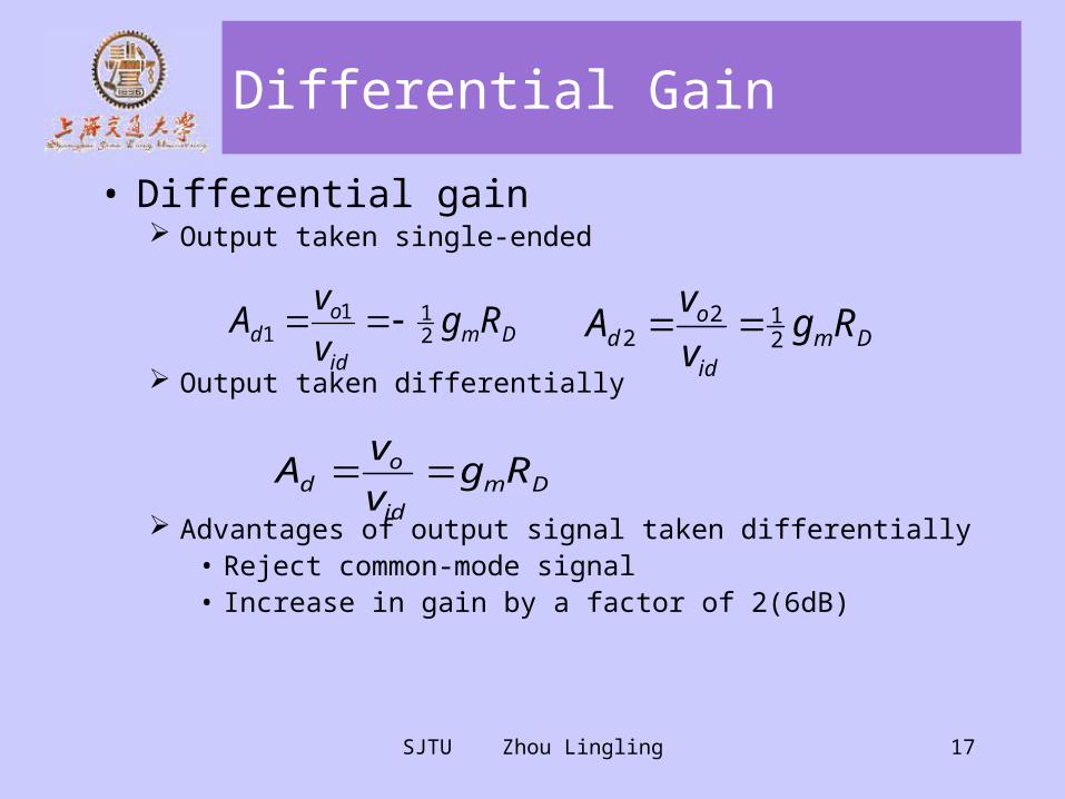
Differential Gain
• Differential gain Output taken single-ended
Output taken differentially
Advantages of output signal taken differentially• Reject common-mode signal• Increase in gain by a factor of 2(6dB)
Dmid
od Rg
v
vA 2
111
Dmid
od Rg
v
vA 2
122
Dmid
od Rg
v
vA

SJTU Zhou Lingling 18
Differential Gain
MOS differential amplifier with ro and RSS taken into account.
SJTU Zhou Lingling 19
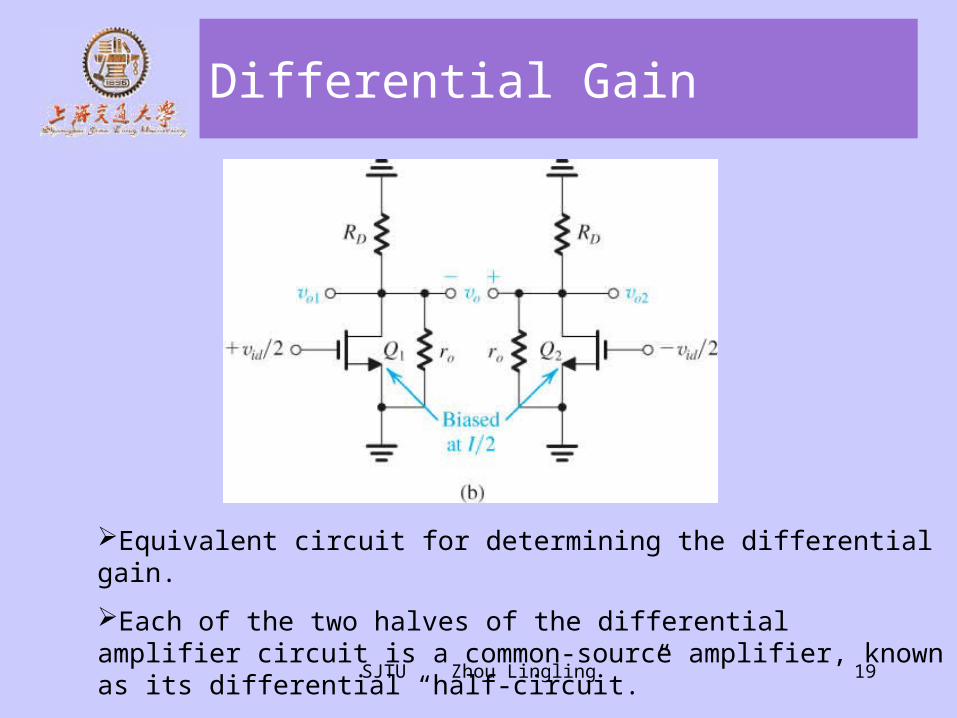
Differential Gain
Equivalent circuit for determining the differential gain.
Each of the two halves of the differential amplifier circuit is a common-source amplifier, known as its differential “half-circuit.”

SJTU Zhou Lingling 20
Differential Gain
• Differential gain Output taken single-ended
Output taken differentially
)//(211
1 oDmid
od rRg
v
vA )//(2
122 oDm
id
od rRg
v
vA
)//( oDmid
od rRg
v
vA
SJTU Zhou Lingling 21
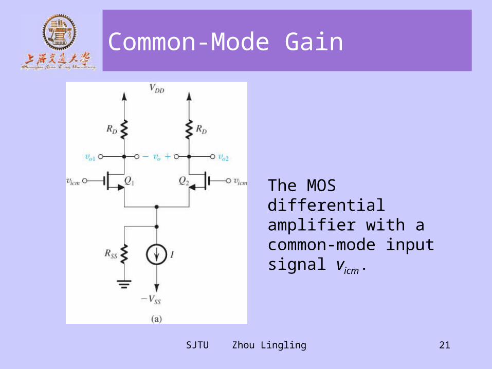
Common-Mode Gain
The MOS differential amplifier with a common-mode input signal vicm.

SJTU Zhou Lingling 22
Common-Mode Gain
Equivalent circuit for determining the common-mode gain (with ro ignored).
Each half of the circuit is known as the “common-mode half-circuit.”

SJTU Zhou Lingling 23
Common-Mode Gain
• Common-mode gain Output taken single-ended
Output taken differentially
ss
D
ssm
D
icm
o
icm
ocmcm R
R
Rg
R
v
v
v
vAA
221
2121
012
icm
oocm v
vvA

SJTU Zhou Lingling 24
Common-Mode Rejection Ratio
• Common-mode rejection ratio(CMRR) Output taken single-ended
Output taken differentially
This is true only when the circuit is perfectly matched.
CMRR
ssmcm
d
cm
d RgA
A
A
ACMRR
2
2
1
1
SJTU Zhou Lingling 25
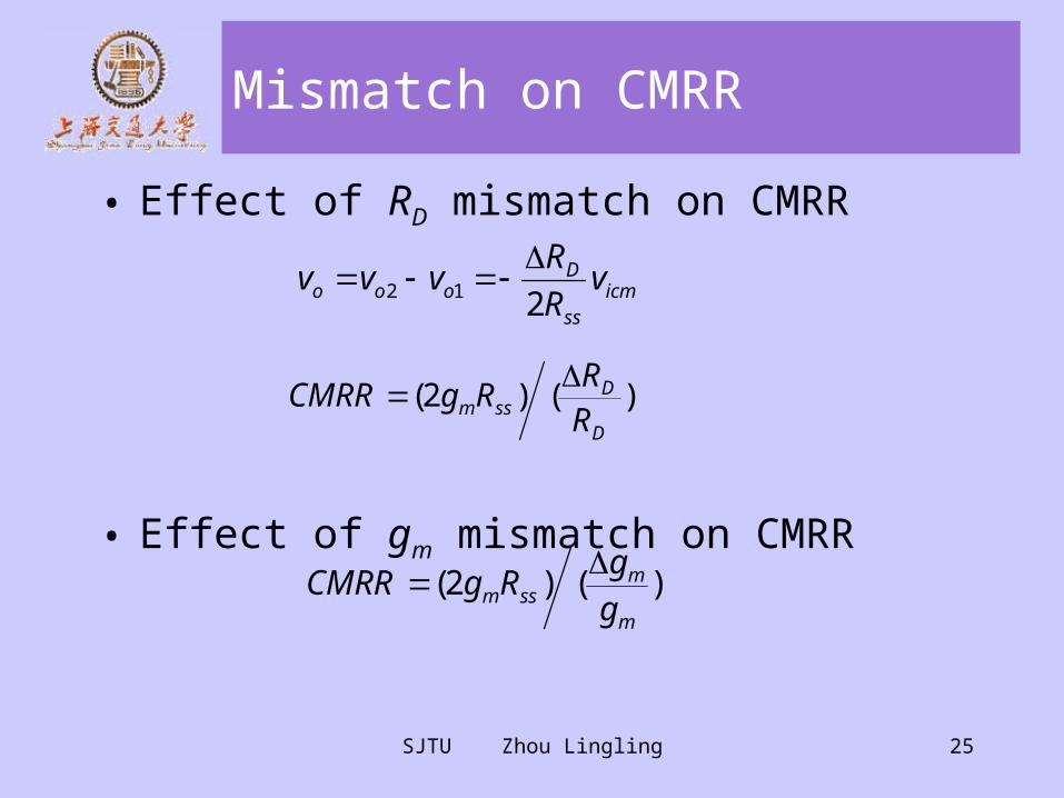
Mismatch on CMRR
• Effect of RD mismatch on CMRR
• Effect of gm mismatch on CMRR
icmss
Dooo v
R
Rvvv
212
)()2(D
Dssm R
RRgCMRR
)()2(m
mssm g
gRgCMRR

SJTU Zhou Lingling 26
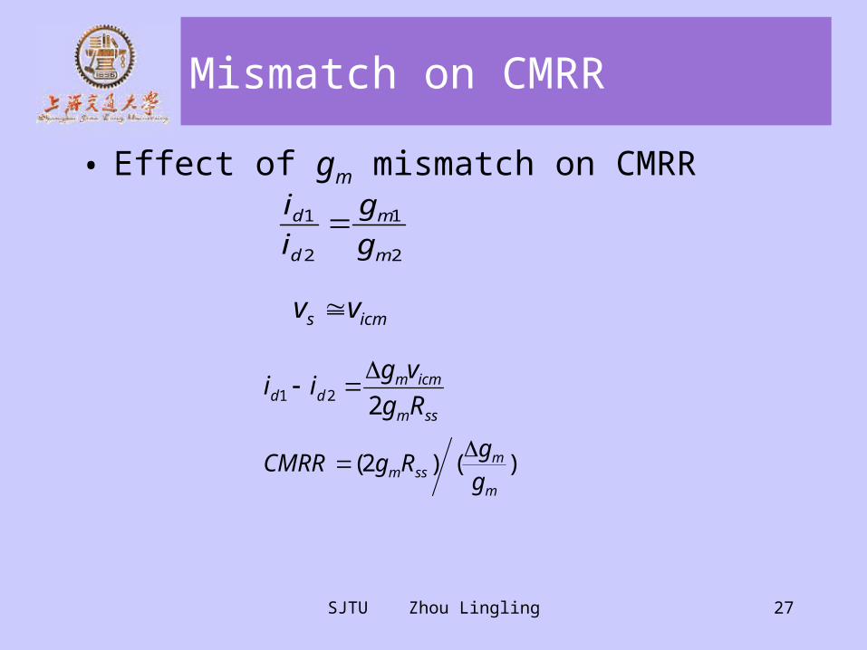
Mismatch on CMRR
Determine the common-mode gain resulting from a mismatch in the gm values of Q1 and Q2.
Common-mode half circuit is not available due to mismatch in circuit.
The nominal value gm.
SJTU Zhou Lingling 27
Mismatch on CMRR
• Effect of gm mismatch on CMRR
2
1
2
1
m
m
d
d
g
g
i
i
icms vv
ssm
icmmdd Rg
vgii
221
)()2(m
mssm g
gRgCMRR
SJTU Zhou Lingling 28
The BJT Differential Pair
• Basic operation• Large-signal operation• Small-signal operation
Differential gainCommon-mode gainCommon-mode rejection ration

SJTU Zhou Lingling 29
The BJT Differential Pair
The basic BJT differential-pair configuration.

SJTU Zhou Lingling 30
Basic Operation
The differential pair with a common-mode input signal vCM.
Two transistors are matched.
Current source with infinite output resistance.
Current I divide equally between two transistors.
The difference in voltage between the two collector is zero.
The differential pair rejects the common-mode input signal as long as two transistors remain in active region.

SJTU Zhou Lingling 31
Basic Operation
The differential pair with a “large” differential input signal.
Q1 is on and Q2 is off.
Current I entirely flows in Q1.

SJTU Zhou Lingling 32
Basic Operation
The differential pair with a large differential input signal of polarity opposite to that in (b).
Q2 is on and Q1 is off.
Current I entirely flows in Q2.
SJTU Zhou Lingling 33
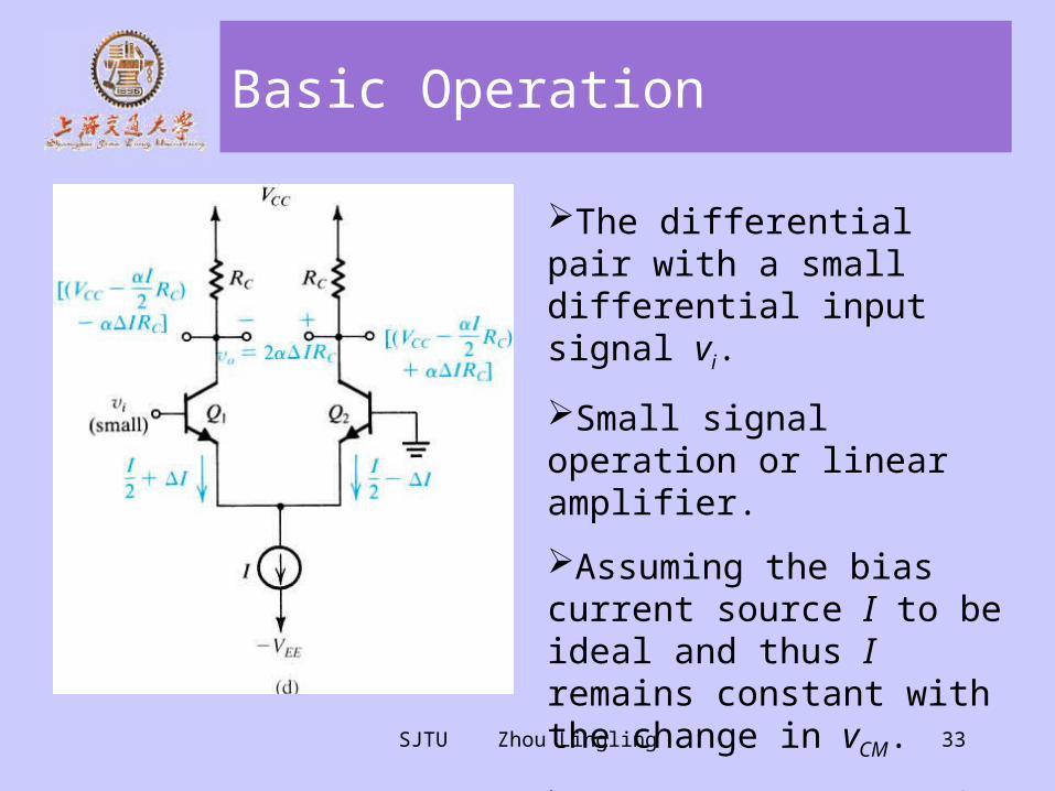
Basic Operation
The differential pair with a small differential input signal vi.
Small signal operation or linear amplifier.
Assuming the bias current source I to be ideal and thus I remains constant with the change in vCM.
Increment in Q1 and decrement in Q2.
SJTU Zhou Lingling 34
Large-Signal Operation
SJTU Zhou Lingling 35
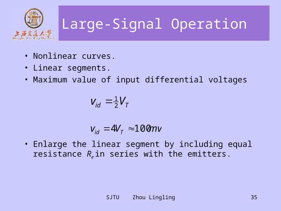
Large-Signal Operation
• Nonlinear curves.
• Linear segments.
• Maximum value of input differential voltages
• Enlarge the linear segment by including equal resistance Re
in series with the emitters.
Tid Vv 21
mvVv Tid 1004

SJTU Zhou Lingling 36
Large-Signal Operation
The transfer characteristics of the BJT differential pair (a) can be linearized by including resistances in the emitters.

SJTU Zhou Lingling 37
Small Signal Operation
The currents and voltages in the differential amplifier when a small differential input signal vid is applied.

SJTU Zhou Lingling 38
Small Signal Operation
A simple technique for determining the signal currents in a differential amplifier excited by a differential voltage signal vid; dc quantities are not shown.

SJTU Zhou Lingling 39
Small Signal Operation
A differential amplifier with emitter resistances.
Only signal quantities are shown (in color).
SJTU Zhou Lingling 40
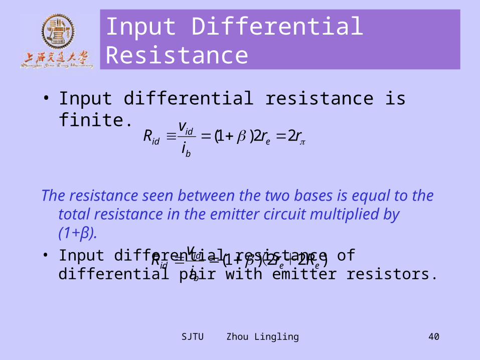
Input Differential Resistance
• Input differential resistance is finite.
The resistance seen between the two bases is equal to the total resistance in the emitter circuit multiplied by (1+β).
• Input differential resistance of differential pair with emitter resistors.
rri
vR e
b
idid 22)1(
)22)1( eeb
idid Rr
i
vR +(

SJTU Zhou Lingling 41
Differential Voltage Gain
• Differential voltage gain Output voltage taken single-ended
Output voltage taken differentially
Cmid
od Rg
v
vA 2
111 Cm
id
od Rg
v
vA 2
122
Cmid
ood Rg
v
vvA
12
SJTU Zhou Lingling 42
Differential Voltage Gain
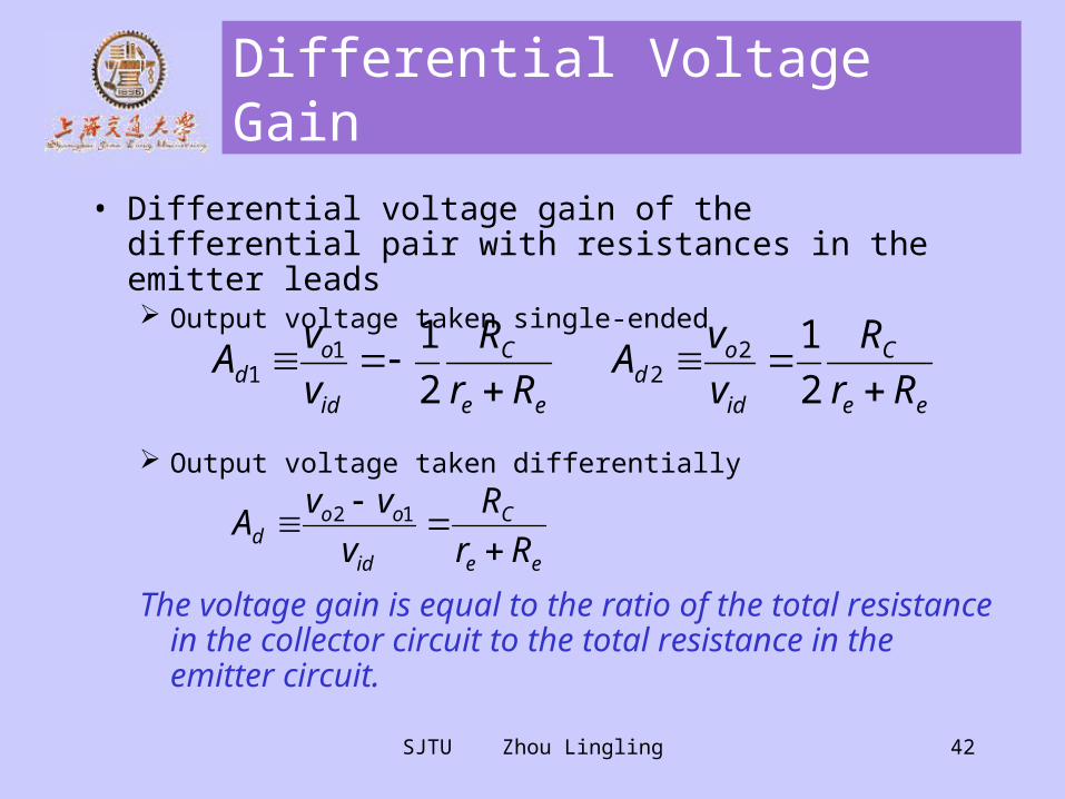
• Differential voltage gain of the differential pair with resistances in the emitter leads Output voltage taken single-ended
Output voltage taken differentially
The voltage gain is equal to the ratio of the total resistance in the collector circuit to the total resistance in the emitter circuit.
ee
C
id
od Rr
R
v
vA
2
111
ee
C
id
ood Rr
R
v
vvA
12
ee
C
id
od Rr
R
v
vA
2
122

SJTU Zhou Lingling 43
Differential Half-Circuit Analysis
Differential input signals.
Single voltage at joint emitters is zero.
The circuit is symmetric.
Equivalent common-emitter amplifiers in (b).

SJTU Zhou Lingling 44
Differential Half-Circuit Analysis
This equivalence applies only for differential input signals.
Either of the two common-emitter amplifiers can be used to find the differential gain, differential input resistance, frequency response, and so on, of the differential amplifier.
Half circuit is biased at I/2.
The voltage gain(with the output taken differentially) is equal to the voltage of half circuit.

SJTU Zhou Lingling 45
Differential Half-Circuit Analysis
The differential amplifier fed in a single-ended fashion.
Signal voltage at the emitter is not zero.
Almost identical to the symmetric one.

SJTU Zhou Lingling 46
Common-Mode Gain
The differential amplifier fed by a common-mode voltage signal vicm.
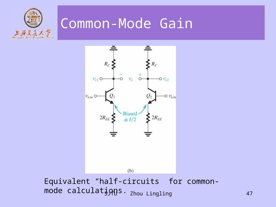
SJTU Zhou Lingling 47
Common-Mode Gain
Equivalent “half-circuits” for common-mode calculations.
SJTU Zhou Lingling 48
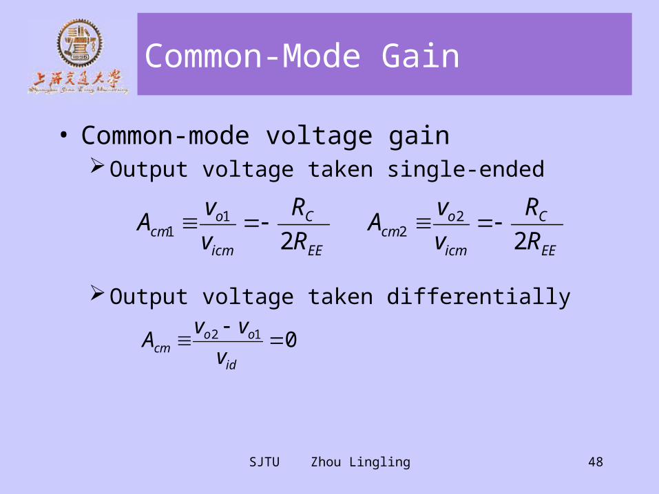
Common-Mode Gain
• Common-mode voltage gainOutput voltage taken single-ended
Output voltage taken differentially
EE
C
icm
ocm R
R
v
vA
21
1
012
id
oocm v
vvA
EE
C
icm
ocm R
R
v
vA
22
2

SJTU Zhou Lingling 49
Common-Mode Rejection Ratio
• Common-mode rejection ratioOutput voltage taken single-ended
Output voltage taken differentially
This is true only when the circuit is symmetric.• Mismatch on CMRR
EEmRgCMRR
CMRR
C
C
EE
Ccm R
R
R
RA
2

SJTU Zhou Lingling 50
Input Common-Mode Resistance
Definition of the input common-mode resistance Ricm.
The equivalent common-mode half-circuit.

SJTU Zhou Lingling 51
Input Common-Mode Resistance
• Input common-mode resistance
• Input common-mode resistance is very large.
)//2)(1(2 oEEicm rRR
)2
//)(1( oEEicm
rRR

SJTU Zhou Lingling 52
Example

SJTU Zhou Lingling 53
Example (cont’d)
Evaluate the following:• The input differential resistance.• The overall differential voltage gain(neglect the
effect of ro).
• The worst-case common-mode gain if the two collector resistance are accurate within ±1%.
• The CMRR, in dB.• The input common-mode resistance(suppose the
Early voltage is 100V).

SJTU Zhou Lingling 54
The Differential Amplifier with Active Load
• Replace resistance RD with a constant current source results in a much high voltage gain as well as saving in chip area.
• Convert the output from differential to single-ended.

SJTU Zhou Lingling 55
Differential-to-Single-Ended Conversion
A simple but inefficient approach for differential to single-ended conversion.
SJTU Zhou Lingling 56
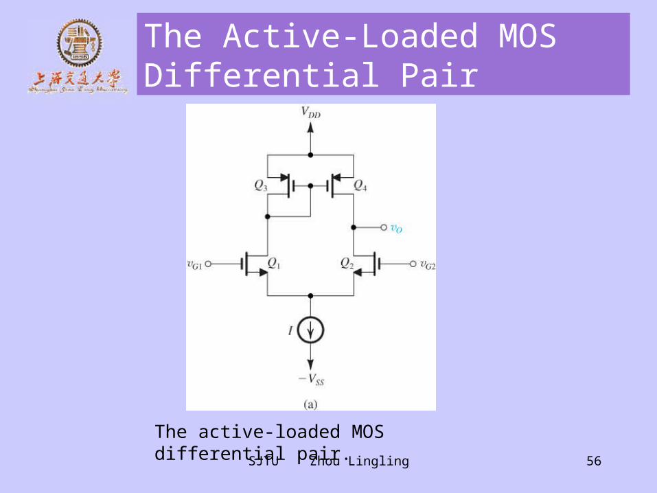
The Active-Loaded MOS Differential Pair
The active-loaded MOS differential pair.

SJTU Zhou Lingling 57
The Active-Loaded MOS Differential Pair
The circuit at equilibrium assuming perfect matching.

SJTU Zhou Lingling 58
The Active-Loaded MOS Differential Pair
The circuit with a differential input signal applied, neglecting the ro of all transistors.

SJTU Zhou Lingling 59
Differential Gain of the Active-Loaded MOS Pair
• The output resistance ro plays a significant role in the operation of active-loaded amplifier.
• Asymmetric circuit.
• Half-circuit is not available.
• The gain will be determined as GmRo

SJTU Zhou Lingling 60
Short-Circuit Transconductance
Determining the short-circuit transconductance Gm = io/vid

SJTU Zhou Lingling 61
Short-Circuit Transconductance
mm gG

SJTU Zhou Lingling 62
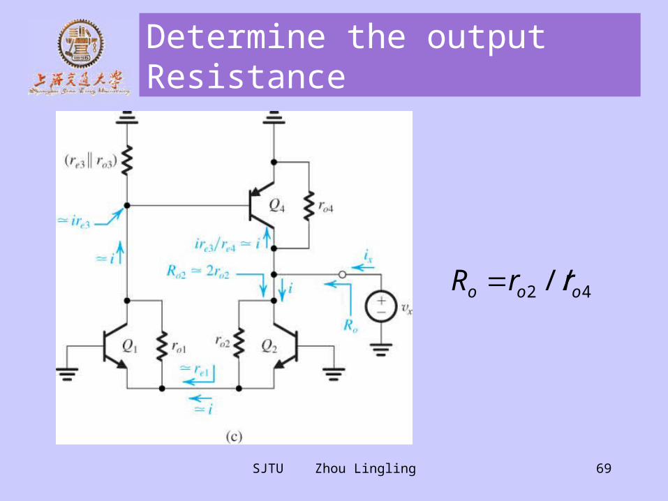
Output Resistance
Circuit for determining Ro. The circled numbers indicate the order of the analysis steps.

SJTU Zhou Lingling 63
Output Resistance
Circuit for determining Ro.
The circled numbers indicate the order of the analysis steps.
42 // ooo rrR

SJTU Zhou Lingling 64
Differential Gain
• The differential gain is determined as GmRo
• When
)42 //( oomomd rrgRGA
ooo rrr 42
20
21 A
rgA omd

SJTU Zhou Lingling 65
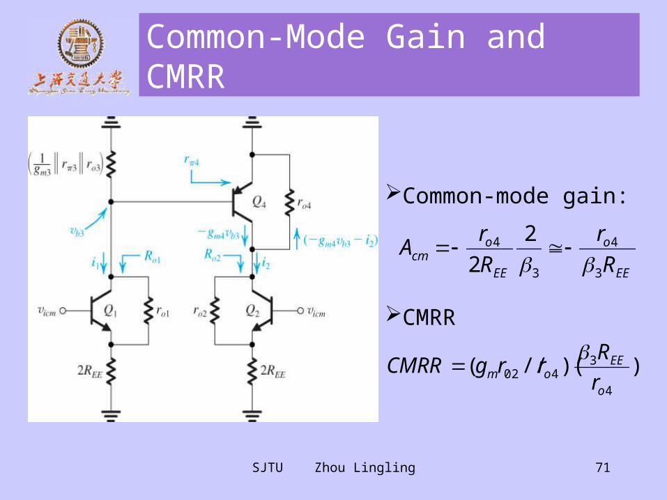
Common-Mode Gain and CMRR
Analysis of the active-loaded MOS differential amplifier to determine its common-mode gain.
Power supplies eliminated.
Rss is the output resistance of the current source.

SJTU Zhou Lingling 66
Common-Mode Gain and CMRR
Asymmetric circuit.
Each of the two transistors as a CS configuration with a large source degeneration resistance 2Rss.
Common-mode gain:
CMRR
ssmm
o
sscm Rgrg
r
RA
3033
4
2
1
12
1
))(( ssmom RgrgCMRR

SJTU Zhou Lingling 67
The Bipolar Differential Pair with Active Load
Active-loaded bipolar differential pair.

SJTU Zhou Lingling 68
Determine the Transconductance
mm gG
SJTU Zhou Lingling 69
Determine the output Resistance
42 // ooo rrR

SJTU Zhou Lingling 70
Differential Gain
• The differential gain is determined as GmRo
• When
• Input differential resistance
)42 //( oomomd rrgRGA
20
21 A
rgA omd
ooo rrr 42
rRid 2
SJTU Zhou Lingling 71
Common-Mode Gain and CMRR
Common-mode gain:
CMRR
EE
o
EE
ocm R
r
R
rA
3
4
3
4 2
2
))(//(4
3402
o
EEom r
RrrgCMRR

SJTU Zhou Lingling 72
Frequency Response of the Resistively Loaded MOS Amplifier
A resistively loaded MOS differential pair with the transistor supplying the bias current explicitly shown.
It is assumed that the total impedance between node S and ground, ZSS, consists of a resistance RSS in parallel with a capacitance CSS.

SJTU Zhou Lingling 73
Frequency Response of the Resistively Loaded MOS Amplifier
(b) Differential half-circuit. (c) Common-mode half-circuit.

SJTU Zhou Lingling 74
Frequency Response of the Resistively Loaded MOS Amplifier
common-mode gain

SJTU Zhou Lingling 75
Frequency Response of the Resistively Loaded MOS Amplifier
Differential Gain

SJTU Zhou Lingling 76
Frequency Response of the Resistively Loaded MOS Amplifier
CMRR with frequency.

SJTU Zhou Lingling 77
Multistage Amplifier
• A four-stage bipolar op amplifier
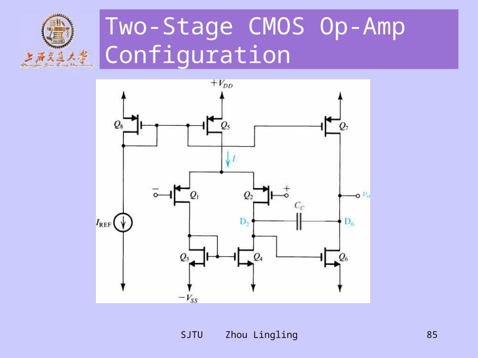
• A two-stage CMOS op amplifier
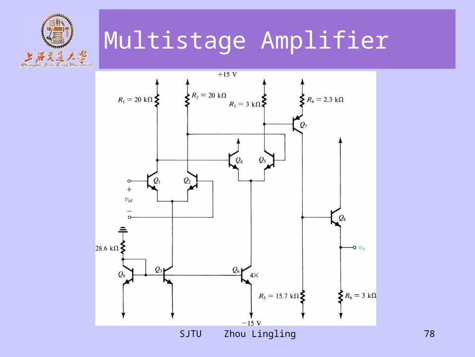
SJTU Zhou Lingling 78
Multistage Amplifier
SJTU Zhou Lingling 79
Multistage Amplifier
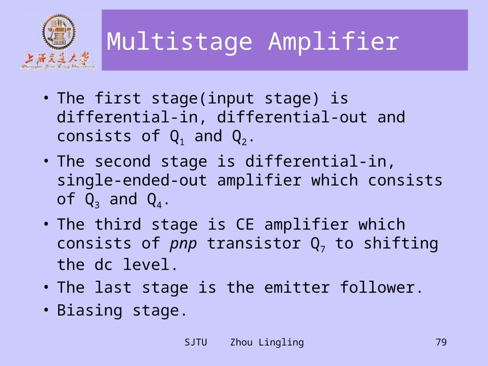
• The first stage(input stage) is differential-in, differential-out and consists of Q1 and Q2.
• The second stage is differential-in, single-ended-out amplifier which consists of Q3 and Q4.
• The third stage is CE amplifier which consists of pnp transistor Q7 to shifting the dc level.
• The last stage is the emitter follower. • Biasing stage.
SJTU Zhou Lingling 80

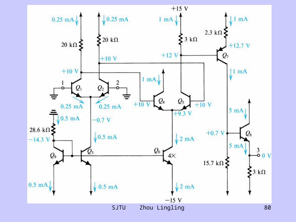
SJTU Zhou Lingling 81
Multistage Amplifier
Equivalent circuit for calculating the gain of the input stage of the example.
Input differential resistance
Gain of first stage
krRid 2.202 1
4.22)//(
21
212011
ee
i
id rr
RRR
v
vA

SJTU Zhou Lingling 82
Multistage Amplifier
Equivalent circuit for calculating the gain of the second stage of the example.
Gain of second stage
2.59//
54
33
01
022
ee
i
rr
RR
v
vA

SJTU Zhou Lingling 83
Multistage Amplifier
Equivalent circuit for calculating the gain of the third stage of the example.
Gain of third stage
42.6//
47
54
02
033
Rr
RR
v
vA
e
i

SJTU Zhou Lingling 84
Multistage Amplifier
Equivalent circuit for calculating the gain of the output stage of the example.
Gain of output stage
Output resistance
998.068
6
03
04
Rr
R
v
vA
e
152)1(// 586 RrRR eo
SJTU Zhou Lingling 85
Two-Stage CMOS Op-Amp Configuration
Related Documents