SISTEMI EMBEDDED AA 2014/2015 Nios II Characteris;cs and Architecture Federico Baron;

Welcome message from author
This document is posted to help you gain knowledge. Please leave a comment to let me know what you think about it! Share it to your friends and learn new things together.
Transcript
SISTEMI EMBEDDED AA 2014/2015
Nios II Characteris;cs and Architecture
Federico Baron;
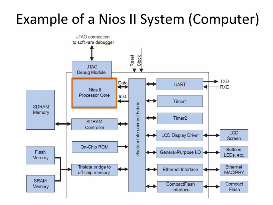
Example of a Nios II System (Computer)

Nios II Main Characteris;cs
• RISC architecture (all instruc;ons are 32-‐bit long) • 32-‐bit data word. Data are handled in word, half-‐word, and byte
• Byte-‐addressable memory space: – with liQle-‐endian addressing scheme (lower byte addresses used for less significant bytes)
– The LOAD and STORE instruc;ons can transfer data in word, half-‐word, and byte
• 32 general-‐purpose registers, 32-‐bit long • Several addi;onal control registers

Nios II Other Characteris;cs (1)
• Op;onal shadow register sets • 32 interrupt sources • External interrupt controller interface for more interrupt sources
• Single-‐instruc;on 32 × 32 mul;ply and divide producing a 32-‐bit result
• Dedicated instruc;ons for compu;ng 64-‐bit and 128-‐bit products of mul;plica;on

Nios II Other Characteris;cs (2)
• Floa;ng-‐point instruc;ons for single-‐precision floa;ng-‐point opera;ons
• Single-‐instruc;on barrel shiZer • Hardware-‐assisted debug module enabling processor start, stop, step, and trace under control of the Nios II soZware development tools
• Op;onal memory management unit (MMU) to support opera;ng systems that require MMUs

Nios II Characteris;cs (3)
• Op;onal memory protec;on unit (MPU) • SoZware development environment based on the GNU C/C++ tool chain and the Nios II SoZware Build Tools (SBT) for Eclipse
• Integra;on with Altera's SignalTap® II Embedded Logic Analyzer, enabling real-‐;me analysis of instruc;ons and data along with other signals in the FPGA design
• Instruc;on set architecture (ISA) compa;ble across all Nios II processor versions – Performance up to 250 DMIPS
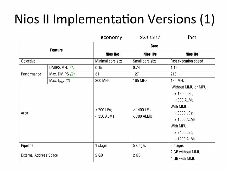
Nios II Implementa;on Versions (1)
Nios II Processor Reference HandbookMay 2011
NII51015-11.0.0
Subscribe
© 2011 Altera Corporation. All rights reserved. ALTERA, ARRIA, CYCLONE, HARDCOPY, MAX, MEGACORE, NIOS, QUARTUS and STRATIX are Reg. U.S. Pat. & Tm. Off. and/or trademarks of Altera Corporation in the U.S. and other countries. All other trademarks and service marks are the property of their respective holders as described at www.altera.com/common/legal.html. Altera warrants performance of its semiconductor products to current specifications in accordance with Altera’s standard warranty, but reserves the right to make changes to any products and services at any time without notice. Altera assumes no responsibility or liability arising out of the application or use of any information, product, or service described herein except as expressly agreed to in writing by Altera. Altera customers are advised to obtain the latest version of device specifications before relying on any published information and before placing orders for products or services.
5. Nios II Core Implementation Details
This document describes all of the Nios® II processor core implementations available at the time of publishing. This document describes only implementation-specific features of each processor core. All cores support the Nios II instruction set architecture.
f For more information regarding the Nios II instruction set architecture, refer to the Instruction Set Reference chapter of the Nios II Processor Reference Handbook.
For common core information and details on a specific core, refer to the appropriate section:
■ “Device Family Support” on page 5–3
■ “Nios II/f Core” on page 5–4
■ “Nios II/s Core” on page 5–14
■ “Nios II/e Core” on page 5–19
Table 5–1 compares the objectives and features of each Nios II processor core. The table is designed to help system designers choose the core that best suits their target application.
Table 5–1. Nios II Processor Cores (Part 1 of 3)
FeatureCore
Nios II/e Nios II/s Nios II/f
Objective Minimal core size Small core size Fast execution speed
Performance
DMIPS/MHz (1) 0.15 0.74 1.16
Max. DMIPS (2) 31 127 218
Max. fMAX (2) 200 MHz 165 MHz 185 MHz
Area < 700 LEs;
< 350 ALMs
< 1400 LEs;
< 700 ALMs
Without MMU or MPU:
< 1800 LEs;
< 900 ALMs
With MMU:
< 3000 LEs;
< 1500 ALMs
With MPU:
< 2400 LEs;
< 1200 ALMs
Pipeline 1 stage 5 stages 6 stages
External Address Space 2 GB 2 GB2 GB without MMU
4 GB with MMU
May 2011NII51015-11.0.0
standard economy fast

Nios II Implementa;on Versions (2) 5–2 Chapter 5: Nios II Core Implementation Details
Nios II Processor Reference Handbook May 2011 Altera Corporation
Instruction Bus
Cache – 512 bytes to 64 KB 512 bytes to 64 KB
Pipelined Memory Access – Yes Yes
Branch Prediction – Static Dynamic
Tightly-Coupled Memory – Optional Optional
Data Bus
Cache – – 512 bytes to 64 KB
Pipelined Memory Access – – –
Cache Bypass Methods – –
■ I/O instructions
■ Bit-31 cache bypass
■ Optional MMU
Tightly-Coupled Memory – – Optional
Arithmetic Logic Unit
Hardware Multiply – 3-cycle (3) 1-cycle (3)
Hardware Divide – Optional Optional
Shifter 1 cycle-per-bit 3-cycle shift (3)1-cycle barrel
shifter (3)
JTAG Debug Module
JTAG interface, run control, software breakpoints Optional Optional Optional
Hardware Breakpoints – Optional Optional
Off-Chip Trace Buffer – Optional Optional
Memory Management Unit – – Optional
Memory Protection Unit – – Optional
Exception Handling
Exception Types
Software trap, unimplemented instruction, illegal instruction, hardware interrupt
Software trap, unimplemented instruction, illegal instruction, hardware interrupt
Software trap, unimplemented instruction, illegal instruction, supervisor-only instruction, supervisor-only instruction address, supervisor-only data address, misaligned destination address, misaligned data address, division error, fast TLB miss, double TLB miss, TLB permission violation, MPU region violation, internal hardware interrupt, external hardware interrupt, nonmaskable interrupt
Integrated Interrupt Controller Yes Yes Yes
External Interrupt Controller Interface No No Optional
Table 5–1. Nios II Processor Cores (Part 2 of 3)
FeatureCore
Nios II/e Nios II/s Nios II/f

Dhrystone Benchmark (1) • Problem: compare processors with very different architectures in a way representa9ve of real-‐world applica9ons – MIPS are unsuitable to compare RISC with CISC processors, which have very different instruc;on sets
• Dhrystone benchmark was first published in Ada back to 1984
• Now the C version of Dhrystone is largely used in industry

Dhrystone Benchmark (2) • Dhrystone compares the performance of the processor under benchmark to that of a reference machine
• Dhrystone code dominated by simple integer arithme;c opera;ons, string opera;ons, logic decisions, and memory accesses
• Dhrystone result is determined by measuring the average ;me a processor takes to perform many itera;ons of a single loop containing a fixed sequence of instruc;ons that make up the benchmark
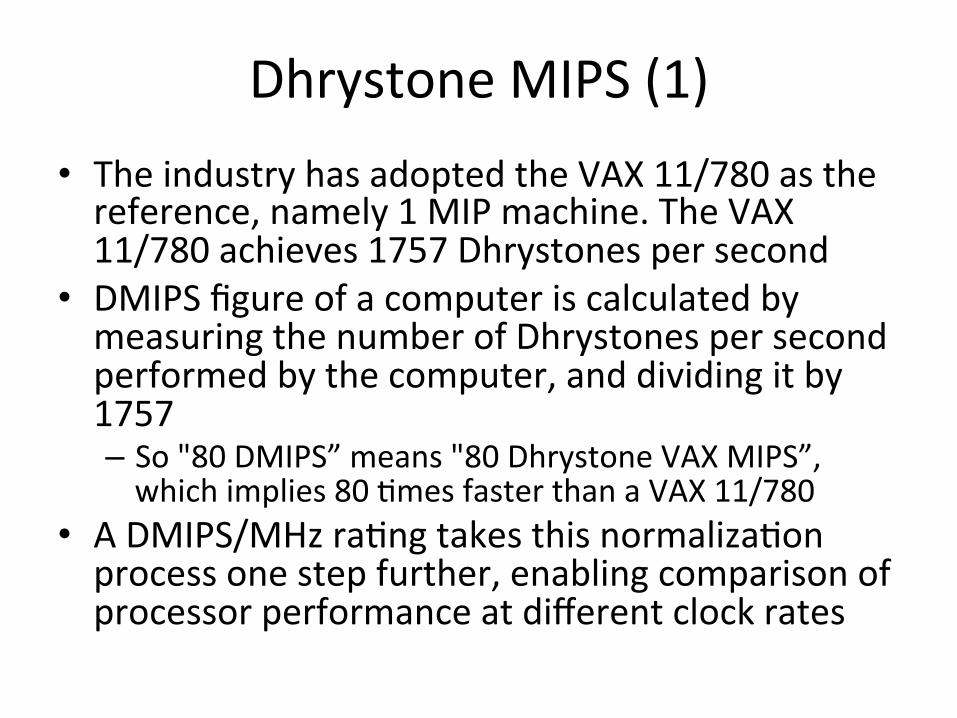
Dhrystone MIPS (1) • The industry has adopted the VAX 11/780 as the reference, namely 1 MIP machine. The VAX 11/780 achieves 1757 Dhrystones per second
• DMIPS figure of a computer is calculated by measuring the number of Dhrystones per second performed by the computer, and dividing it by 1757 – So "80 DMIPS” means "80 Dhrystone VAX MIPS”, which implies 80 ;mes faster than a VAX 11/780
• A DMIPS/MHz ra;ng takes this normaliza;on process one step further, enabling comparison of processor performance at different clock rates

Dhrystone MIPS (2)
• Dhrystone numbers actually reflect the performance of the C compiler and libraries, probably more than the performance of the processor itself. Also, lack of independent cer;fica;on means that customers are dependent on processor vendors to quote accurate and meaningful Dhrystone data.

“And of course, the very success of a benchmark program is a danger in that people may tune their compilers and/or hardware to it, and with this ac;on make it less useful.” Reinhold P. Weicker, Siemens AG, April 1989 Author of the Dhrystone Benchmark

Nios II registers (1) • General-‐purpose registers (r0-‐r31)
3–10 Chapter 3: Programming ModelRegisters
Nios II Processor Reference Handbook May 2011 Altera Corporation
Default CacheabilityThe default cacheability specifies whether normal load and store instructions access the data cache or bypass the data cache. The default cacheability is only present for data regions. You can override the default cacheability by using the ldio or stio instructions. The bit 31 cache bypass feature is available when the MPU is present. Refer to “Cache Memory” on page 3–53 for more information on cache bypass.
Overlapping RegionsThe memory addresses of regions can overlap. Overlapping regions have several uses including placing markers or small holes inside of a larger region. For example, the stack and heap may be located in the same region, growing from opposite ends of the address range. To detect stack/heap overflows, you can define a small region between the stack and heap with no access permissions and assign it a higher priority than the larger region. Any access attempts to the hole region trigger an exception informing system software about the stack/heap overflow.
If regions overlap so that a particular access matches more than one region, the region with the highest priority (lowest index) determines the access permissions and default cacheability.
Enabling the MPUThe MPU is disabled on system reset. System software enables and disables the MPU by writing to a control register. Before enabling the MPU, you must create at least one instruction and one data region, otherwise unexpected results can occur. Refer to “Working with the MPU” on page 3–29 for more information.
RegistersThe Nios II register set includes general-purpose registers and control registers. In addition, the Nios II/f core can optionally have shadow register sets. This section discusses each register type.
General-purpose RegistersThe Nios II architecture provides thirty-two 32-bit general-purpose registers, r0 through r31, as described in Table 3–5. Some registers have names recognized by the assembler. For example, the zero register (r0) always returns the value zero, and writing to zero has no effect. The ra register (r31) holds the return address used by procedure calls and is implicitly accessed by the call, callr and ret instructions. C and C++ compilers use a common procedure-call convention, assigning specific meaning to registers r1 through r23 and r26 through r28.
Table 3–5. The Nios II General-Purpose Registers (Part 1 of 2)
Register Name Function Register Name Function
r0 zero 0x00000000 r16 Callee-saved register
r1 at Assembler temporary r17 Callee-saved register
r2 Return value r18 Callee-saved register
r3 Return value r19 Callee-saved register
Chapter 3: Programming Model 3–11Registers
May 2011 Altera Corporation Nios II Processor Reference Handbook
f For more information, refer to the Application Binary Interface chapter of the Nios II Processor Reference Handbook.
Control RegistersControl registers report the status and change the behavior of the processor. Control registers are accessed differently than the general-purpose registers. The special instructions rdctl and wrctl provide the only means to read and write to the control registers and are only available in supervisor mode.
1 When writing to control registers, all undefined bits must be written as zero.
The Nios II architecture supports up to 32 control registers. Table 3–6 lists details of the defined control registers. All nonreserved control registers have names recognized by the assembler.
r4 Register arguments r20 Callee-saved register
r5 Register arguments r21 Callee-saved register
r6 Register arguments r22 Callee-saved register
r7 Register arguments r23 Callee-saved register
r8 Caller-saved register r24 et Exception temporary
r9 Caller-saved register r25 bt Breakpoint temporary (1)
r10 Caller-saved register r26 gp Global pointer
r11 Caller-saved register r27 sp Stack pointer
r12 Caller-saved register r28 fp Frame pointer
r13 Caller-saved register r29 ea Exception return address
r14 Caller-saved register r30 ba Breakpoint return address (2)
r15 Caller-saved register r31 ra Return address
Notes to Table 3–5:(1) r25 is used exclusively by the JTAG debug module. It is used as the breakpoint temporary (bt) register in the normal register set. In shadow
register sets, r25 is reserved.(2) r30 is used as the breakpoint return address (ba) in the normal register set, and as the shadow register set status (sstatus) in each shadow
register set. For details about sstatus, refer to “The sstatus Register” on page 3–27.
Table 3–5. The Nios II General-Purpose Registers (Part 2 of 2)
Register Name Function Register Name Function
Table 3–6. Control Register Names and Bits (Part 1 of 2)
Register Name Register Contents
0 status Refer to Table 3–7 on page 3–12
1 estatus Refer to Table 3–9 on page 3–14
2 bstatus Refer to Table 3–10 on page 3–15
3 ienable Internal interrupt-enable bits (3)
4 ipending Pending internal interrupt bits (3)
5 cpuid Unique processor identifier
6 Reserved Reserved
7 exception Refer to Table 3–12 on page 3–16

Nios II registers (2) • Control registers accessible only by the special instruc;ons rdctl and
wrctl that are only available in supervisor mode
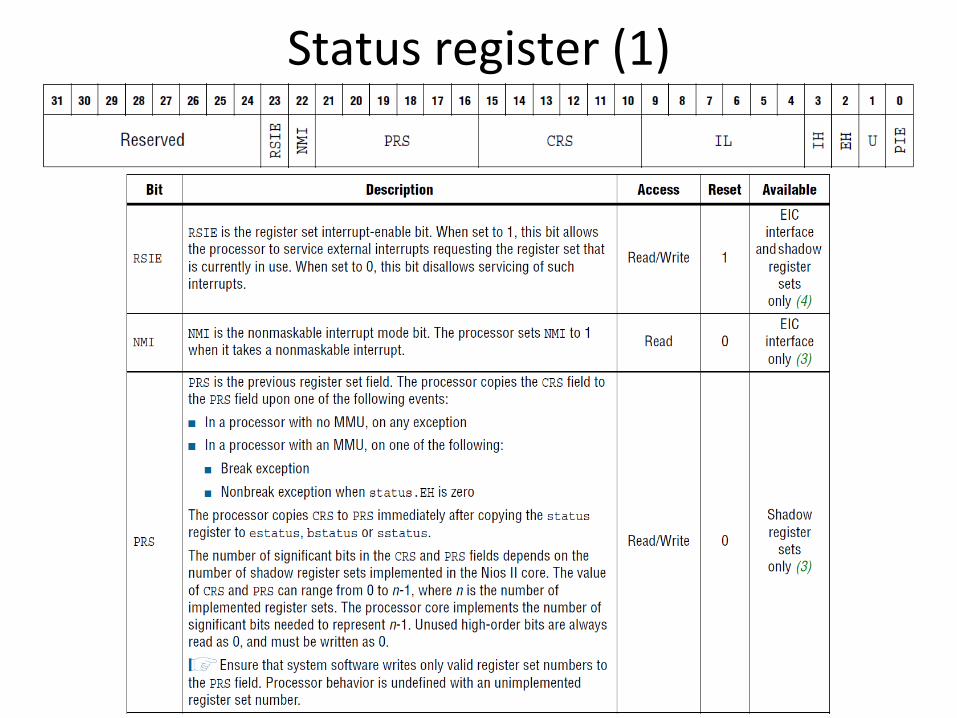
Status register (1)
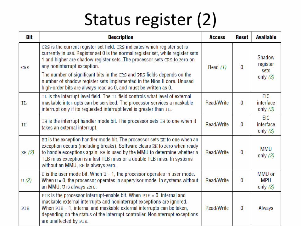
Status register (2)

Other control registers (1)
• The estatus register holds a saved copy of the status register during nonbreak excep;on processing
• The bstatus register holds a saved copy of the status register during break excep;on processing
• The ienable register controls the handling of internal hardware interrupts
• The ipending register indicates the value of the interrupt signals driven into the processor

Other control registers (2)
• The cpuid register holds a constant value that is defined in the Nios II Processor parameter editor to uniquely iden;fy each processor in a mul;processor system
• When the extra excep;on informa;on op;on is enabled, the Nios II processor provides informa;on useful to system soZware for excep;on processing in the excep;on and badaddr registers when an excep;on occurs
• …
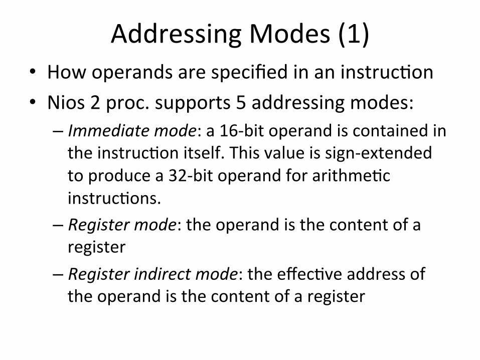
Addressing Modes (1) • How operands are specified in an instruc;on • Nios 2 proc. supports 5 addressing modes:
– Immediate mode: a 16-‐bit operand is contained in the instruc;on itself. This value is sign-‐extended to produce a 32-‐bit operand for arithme;c instruc;ons.
– Register mode: the operand is the content of a register
– Register indirect mode: the effec;ve address of the operand is the content of a register

Addressing Modes (2) • Nios 2 proc. supports 5 addressing modes:
– Displacement mode: the effec;ve address of the operand is obtained by adding the content of a register and a 16-‐bit value contained in the instruc;on itself.
– Absolute mode: is a par;cular case of the Displacement mode when the register is r0
• E.g. addi r3, r2, 100 the content of r2 is added to 100 and the result placed in r3
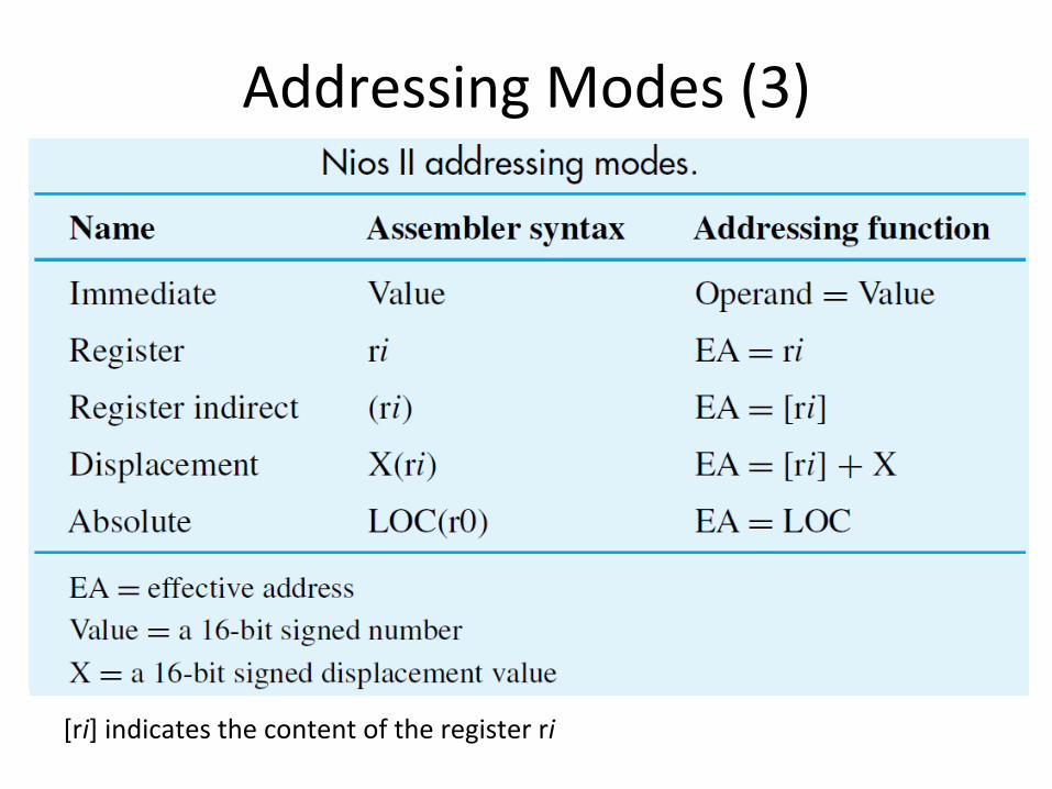
Addressing Modes (3)
[ri] indicates the content of the register ri

Instruc;on formats (1) • RISC-‐style instruc;ons (all 32-‐bit long)
– Load/store architecture for data transfers – Arithme;c/logic instruc;ons use registers
• Three instruc;on types: I-type OP dst_reg, src_reg, immediate R-type OP dst_reg, src_reg1, src_reg1 J-type call label_or_address
• label_or_address is a 26-‐bit unsigned immediate value

Instruc;on formats (2) • I-‐type instruc9ons include arithme;c and logical opera;ons
such as addi and andi; branch opera;ons; load and store opera;ons; and cache management opera;ons.
• R-‐type instruc9ons: include arithme;c and logical opera;ons
such as add and nor; comparison opera;ons such as cmpeq and cmplt
• J-‐type instruc9ons such as call and jmpi, transfer execu;on
anywhere within a 256-‐MB range Nios II Processor Reference HandbookMay 2011
NII51017-11.0.0
Subscribe
© 2011 Altera Corporation. All rights reserved. ALTERA, ARRIA, CYCLONE, HARDCOPY, MAX, MEGACORE, NIOS, QUARTUS and STRATIX are Reg. U.S. Pat. & Tm. Off. and/or trademarks of Altera Corporation in the U.S. and other countries. All other trademarks and service marks are the property of their respective holders as described at www.altera.com/common/legal.html. Altera warrants performance of its semiconductor products to current specifications in accordance with Altera’s standard warranty, but reserves the right to make changes to any products and services at any time without notice. Altera assumes no responsibility or liability arising out of the application or use of any information, product, or service described herein except as expressly agreed to in writing by Altera. Altera customers are advised to obtain the latest version of device specifications before relying on any published information and before placing orders for products or services.
8. Instruction Set Reference
This section introduces the Nios® II instruction word format and provides a detailed reference of the Nios II instruction set. This chapter contains the following sections:
■ “Word Formats” on page 8–1
■ “Instruction Opcodes” on page 8–3
■ “Assembler Pseudo-Instructions” on page 8–4
■ “Assembler Macros” on page 8–5
■ “Instruction Set Reference” on page 8–5
Word FormatsThere are three types of Nios II instruction word format: I-type, R-type, and J-type.
I-TypeThe defining characteristic of the I-type instruction word format is that it contains an immediate value embedded within the instruction word. I-type instructions words contain:
■ A 6-bit opcode field OP
■ Two 5-bit register fields A and B
■ A 16-bit immediate data field IMM16
In most cases, fields A and IMM16 specify the source operands, and field B specifies the destination register. IMM16 is considered signed except for logical operations and unsigned comparisons.
I-type instructions include arithmetic and logical operations such as addi and andi; branch operations; load and store operations; and cache management operations.
Table 8–1 shows the I-type instruction format.
R-TypeThe defining characteristic of the R-type instruction word format is that all arguments and results are specified as registers. R-type instructions contain:
■ A 6-bit opcode field OP
■ Three 5-bit register fields A, B, and C
Table 8–1. I-Type Instruction Format
31 30 29 28 27 26 25 24 23 22 21 20 19 18 17 16 15 14 13 12 11 10 9 8 7 6 5 4 3 2 1 0
A B IMM16 OP
May 2011NII51017-11.0.0
8–2 Chapter 8: Instruction Set ReferenceWord Formats
Nios II Processor Reference Handbook May 2011 Altera Corporation
■ An 11-bit opcode-extension field OPX
In most cases, fields A and B specify the source operands, and field C specifies the destination register.
Some R-Type instructions embed a small immediate value in the five low-order bits of OPX. Unused bits in OPX are always 0.
R-type instructions include arithmetic and logical operations such as add and nor; comparison operations such as cmpeq and cmplt; the custom instruction; and other operations that need only register operands.
Table 8–2 shows the R-type instruction format.
J-TypeJ-type instructions contain:
■ A 6-bit opcode field
■ A 26-bit immediate data field
J-type instructions, such as call and jmpi, transfer execution anywhere within a 256-MB range.
Table 8–3 shows the J-type instruction format.
Table 8–2. R-Type Instruction Format
31 30 29 28 27 26 25 24 23 22 21 20 19 18 17 16 15 14 13 12 11 10 9 8 7 6 5 4 3 2 1 0
A B C OPX OP
Table 8–3. J-Type Instruction Format
31 30 29 28 27 26 25 24 23 22 21 20 19 18 17 16 15 14 13 12 11 10 9 8 7 6 5 4 3 2 1 0
IMM26 OP

Load and Store Instruc;ons • For moving data between memory (or I/O) and general-‐purpose registers
• Words, half-‐words, bytes; alignment required • Variants available for I/O (uncached) access • Examples: ldw r2, 40(r3) // load word stb r6, 4(r12) // store byte ldhio r9, (r20) // load I/O halfword // signed extended ldbu r2, -100(r3) // load byte zero // extended stw r7, 100(r0) // store word

Arithme;c Instruc;ons
• add, addi (16-‐bit immediate is sign-‐extended) • sub, subi, mul, and muli are similar • Mult. is unsigned, result is truncated to 32 bits • div (signed values), divu (unsigned values) • Examples: add r2, r3, r4 //(r2 ← [r3] + [r4]) muli r6, r7, 4096 //(r6 ← [r7] × 4096) divu r8, r9, r10 //(r8 ← [r9] / [r10])
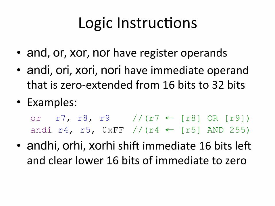
Logic Instruc;ons
• and, or, xor, nor have register operands • andi, ori, xori, nori have immediate operand that is zero-‐extended from 16 bits to 32 bits
• Examples: or r7, r8, r9 //(r7 ← [r8] OR [r9]) andi r4, r5, 0xFF //(r4 ← [r5] AND 255)
• andhi, orhi, xorhi shiZ immediate 16 bits leZ and clear lower 16 bits of immediate to zero
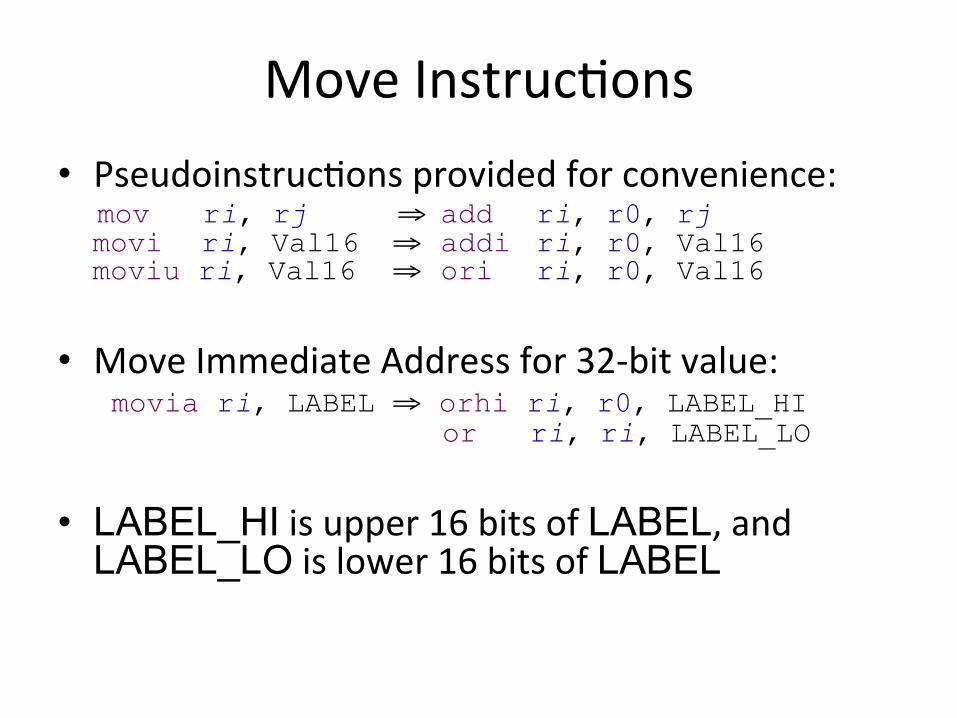
Move Instruc;ons • Pseudoinstruc;ons provided for convenience: mov ri, rj ⇒ add ri, r0, rj movi ri, Val16 ⇒ addi ri, r0, Val16 moviu ri, Val16 ⇒ ori ri, r0, Val16
• Move Immediate Address for 32-‐bit value: movia ri, LABEL ⇒ orhi ri, r0, LABEL_HI or ri, ri, LABEL_LO
• LABEL_HI is upper 16 bits of LABEL, and LABEL_LO is lower 16 bits of LABEL
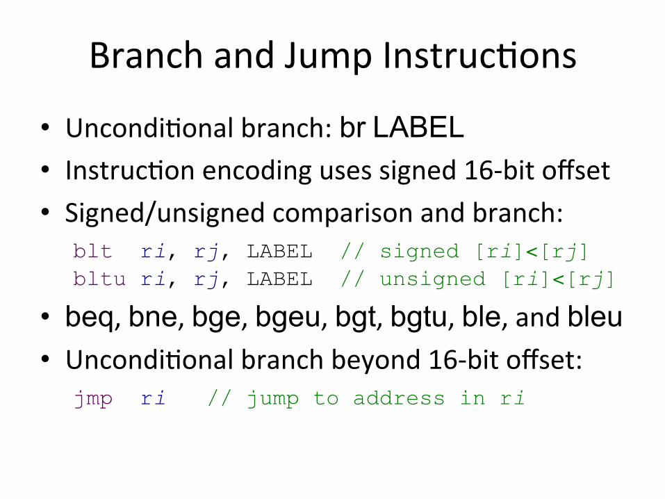
Branch and Jump Instruc;ons
• Uncondi;onal branch: br LABEL • Instruc;on encoding uses signed 16-‐bit offset • Signed/unsigned comparison and branch: blt ri, rj, LABEL // signed [ri]<[rj] bltu ri, rj, LABEL // unsigned [ri]<[rj]
• beq, bne, bge, bgeu, bgt, bgtu, ble, and bleu • Uncondi;onal branch beyond 16-‐bit offset: jmp ri // jump to address in ri
Subrou;ne Linkage Instruc;ons
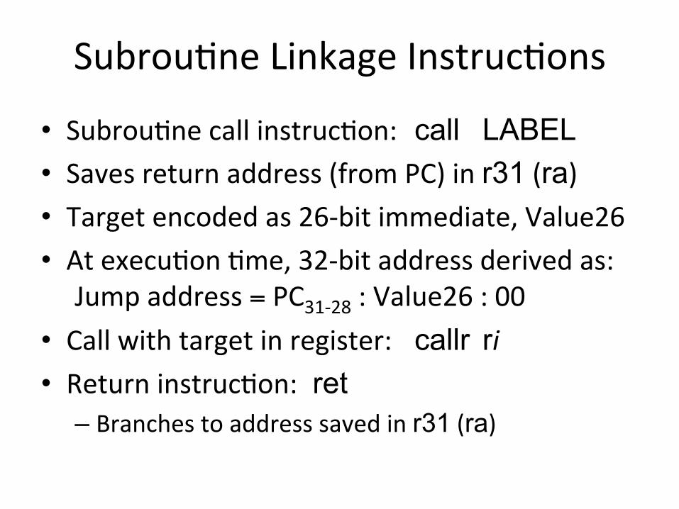
• Subrou;ne call instruc;on: call LABEL • Saves return address (from PC) in r31 (ra) • Target encoded as 26-‐bit immediate, Value26 • At execu;on ;me, 32-‐bit address derived as: Jump address = PC31-‐28 : Value26 : 00
• Call with target in register: callr ri • Return instruc;on: ret
– Branches to address saved in r31 (ra)
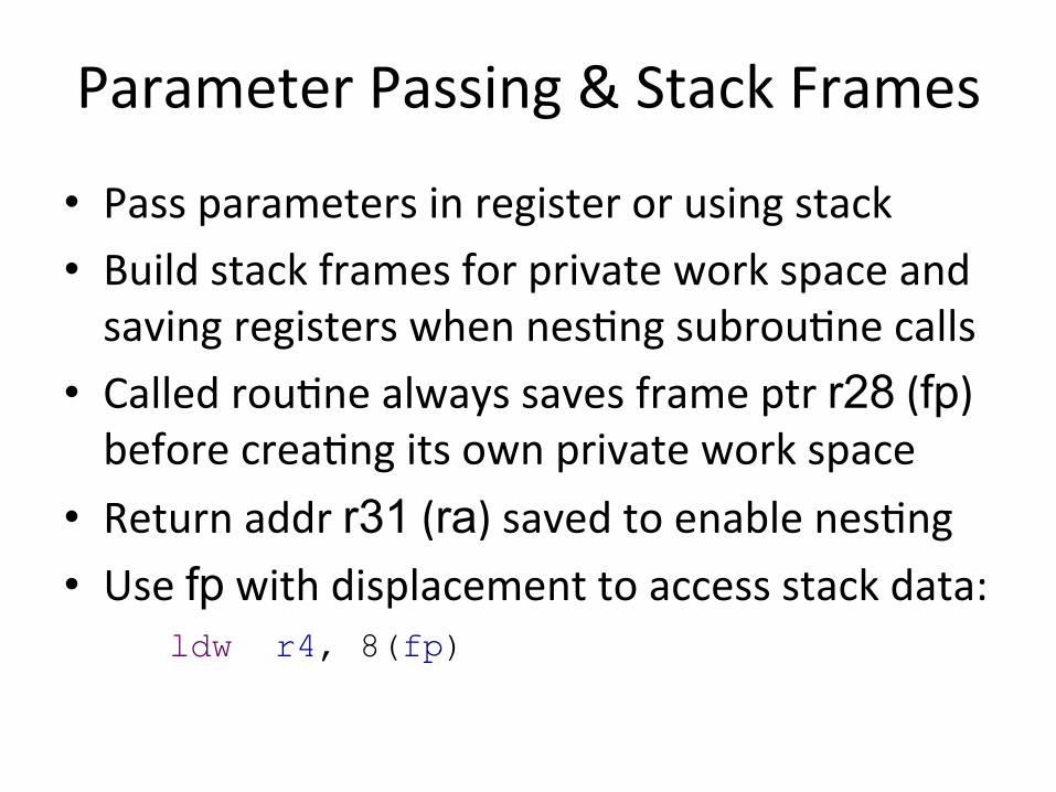
Parameter Passing & Stack Frames
• Pass parameters in register or using stack • Build stack frames for private work space and saving registers when nes;ng subrou;ne calls
• Called rou;ne always saves frame ptr r28 (fp) before crea;ng its own private work space
• Return addr r31 (ra) saved to enable nes;ng • Use fp with displacement to access stack data: ldw r4, 8(fp)
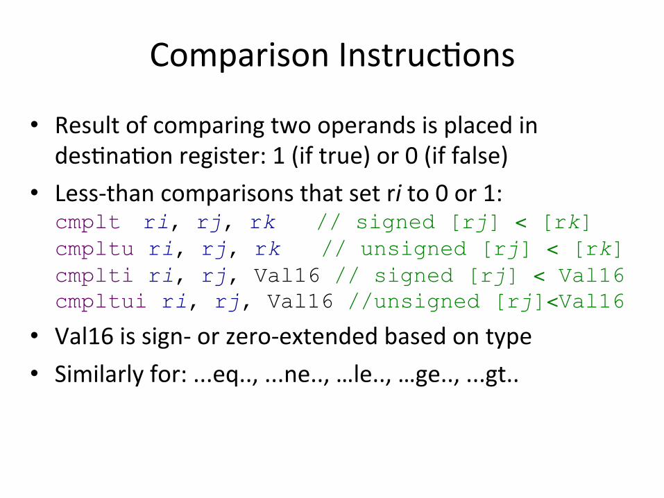
Comparison Instruc;ons
• Result of comparing two operands is placed in des;na;on register: 1 (if true) or 0 (if false)
• Less-‐than comparisons that set ri to 0 or 1: cmplt ri, rj, rk // signed [rj] < [rk] cmpltu ri, rj, rk // unsigned [rj] < [rk] cmplti ri, rj, Val16 // signed [rj] < Val16 cmpltui ri, rj, Val16 //unsigned [rj]<Val16
• Val16 is sign-‐ or zero-‐extended based on type • Similarly for: ...eq.., ...ne.., …le.., …ge.., ...gt..
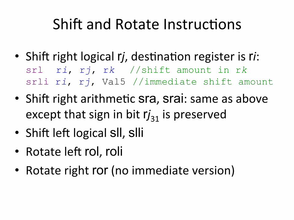
ShiZ and Rotate Instruc;ons
• ShiZ right logical rj, des;na;on register is ri: srl ri, rj, rk //shift amount in rk srli ri, rj, Val5 //immediate shift amount
• ShiZ right arithme;c sra, srai: same as above except that sign in bit rj31 is preserved
• ShiZ leZ logical sll, slli • Rotate leZ rol, roli • Rotate right ror (no immediate version)

Control Instruc;ons
• Special instruc;ons to access control registers • Read Control Register instruc;on: rdctl ri, ctlj // ri ← [ctlj]
• Write Control Register instruc;on: wrctl ctlj, ri // ctlj ← [ri]
• Instruc;ons trap, eret deal with excep;ons (similar to call, ret but for different purpose)
• Addi;onal instruc;ons for cache management

Pseudoinstruc;ons
• mov, movi, and movia already discussed; translated to other instruc;ons by assembler
• Subtract immediate is actually add immediate with nega;on of constant: subi ri, rj, Value16 ⇒ addi ri, rj, -Value16
• Also can swap operands for comparisons: bgt ri, rj, LABEL ⇒ blt rj, ri, LABEL
• Awareness of pseudoinstruc;ons is not cri;cal except when examining assembled code
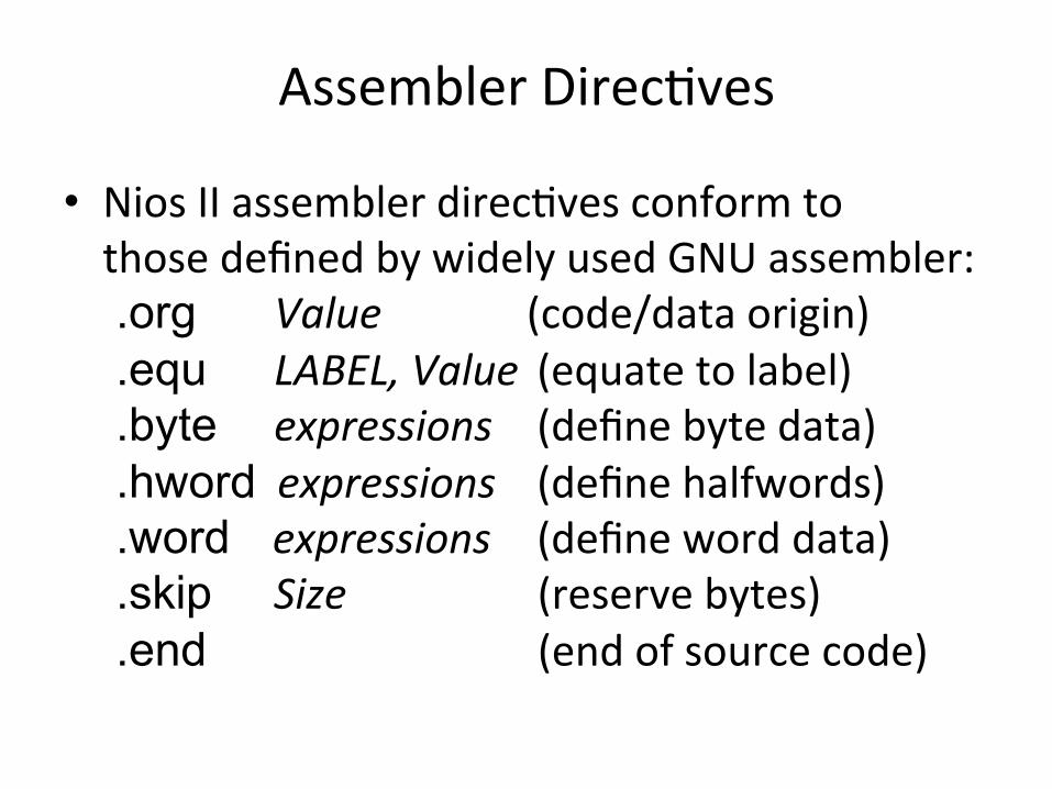
Assembler Direc;ves
• Nios II assembler direc;ves conform to those defined by widely used GNU assembler: .org Value (code/data origin) .equ LABEL, Value (equate to label) .byte expressions (define byte data) .hword expressions (define halfwords) .word expressions (define word data) .skip Size (reserve bytes) .end (end of source code)
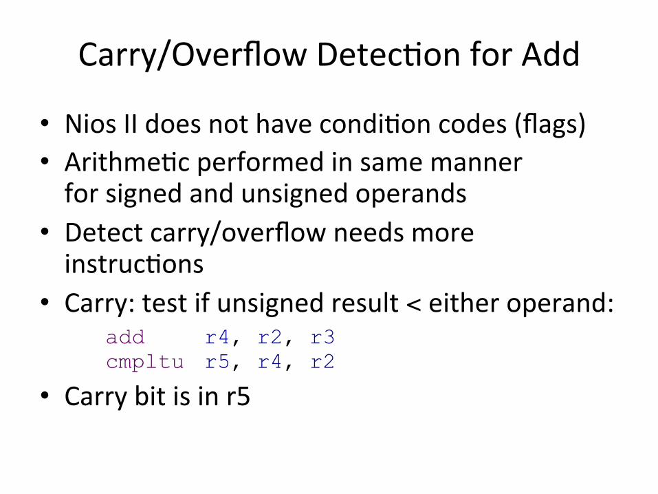
Carry/Overflow Detec;on for Add
• Nios II does not have condi;on codes (flags) • Arithme;c performed in same manner for signed and unsigned operands
• Detect carry/overflow needs more instruc;ons
• Carry: test if unsigned result < either operand: add r4, r2, r3 cmpltu r5, r4, r2
• Carry bit is in r5

Carry/Overflow Detec;on for Add
• Overflow: compare signs of operands & result • Use xor, and to check for same operand signs and different sign for result: add r4, r2, r3 xor r5, r4, r2 xor r6, r4, r3 and r5, r5, r6 blt r5, r0, OVERFLOW
• Similar checks for subtract carry/overflow

Input/Output
• Use I/O versions of Load/Store instruc;ons • Polling for program-‐controlled output:
movia r6, DATA_REG_ADDR mov r7, DATA_TO_SEND movia r4, STATUS_REG_ADDR
L1: ldbio r5, (r4) andi r5, r5, STATUS_FLAG_BIT beq r5, r0, L1 stbio r7, (r6)
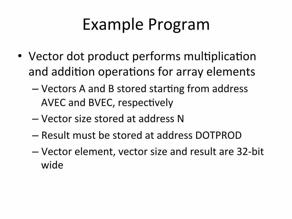
Example Program
• Vector dot product performs mul;plica;on and addi;on opera;ons for array elements – Vectors A and B stored star;ng from address AVEC and BVEC, respec;vely
– Vector size stored at address N – Result must be stored at address DOTPROD – Vector element, vector size and result are 32-‐bit wide


References
• Altera, “Nios II Processor Reference Handbook,” n2cpu_nii5v1.pdf – 2. Processor Architecture – 3. Programming Model/Excep;on Processing – 8. Instruc;on Set Reference
Related Documents