ECE 562 SEPIC Converter (NL5 Simulation) Page 1 SIMULATION WITH THE SEPIC TOPOLOGY (SEPIC-Single Ended Primary Inductance Converter) ECE562: Power Electronics I COLORADO STATE UNIVERSITY Modified in Fall 2011

Welcome message from author
This document is posted to help you gain knowledge. Please leave a comment to let me know what you think about it! Share it to your friends and learn new things together.
Transcript
ECE 562 SEPIC Converter (NL5 Simulation) Page 1
SIMULATION WITH THE SEPIC TOPOLOGY (SEPIC-Single Ended Primary Inductance Converter)
ECE562: Power Electronics I COLORADO STATE UNIVERSITY
Modified in Fall 2011
ECE 562 SEPIC Converter (NL5 Simulation) Page 2
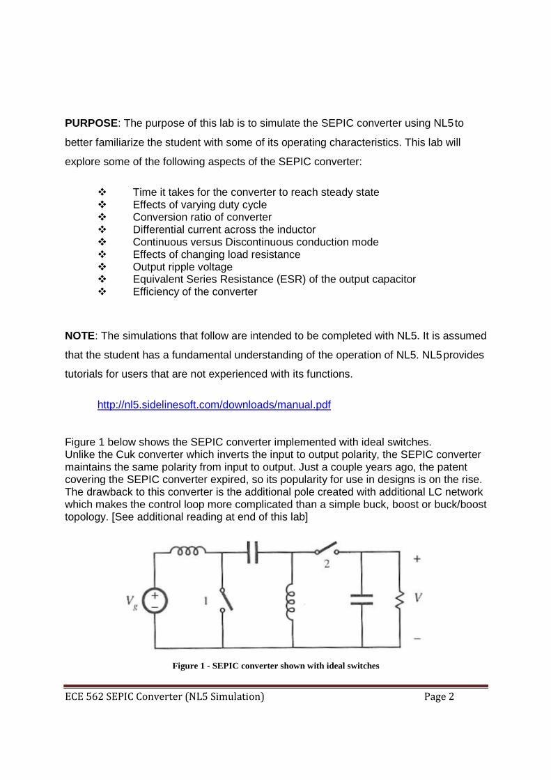
PURPOSE: The purpose of this lab is to simulate the SEPIC converter using NL5
to
better familiarize the student with some of its operating characteristics. This lab will
explore some of the following aspects of the SEPIC converter:
Time it takes for the converter to reach steady state Effects of varying duty cycle Conversion ratio of converter Differential current across the inductor Continuous versus Discontinuous conduction mode Effects of changing load resistance Output ripple voltage Equivalent Series Resistance (ESR) of the output capacitor Efficiency of the converter
NOTE: The simulations that follow are intended to be completed with NL5. It is assumed
that the student has a fundamental understanding of the operation of NL5. NL5
provides
tutorials for users that are not experienced with its functions.
http://nl5.sidelinesoft.com/downloads/manual.pdf Figure 1 below shows the SEPIC converter implemented with ideal switches. Unlike the Cuk converter which inverts the input to output polarity, the SEPIC converter maintains the same polarity from input to output. Just a couple years ago, the patent covering the SEPIC converter expired, so its popularity for use in designs is on the rise. The drawback to this converter is the additional pole created with additional LC network which makes the control loop more complicated than a simple buck, boost or buck/boost topology. [See additional reading at end of this lab]
Figure 1 - SEPIC converter shown with ideal switches

ECE 562 SEPIC Converter (NL5 Simulation) Page 3
The converter shown below is the ‘Inverse’ SEPIC converter. As also is the case for the SEPIC converter, this design also does not invert the input to output polarity. It also has the same (buck/boost) M(D) = D/(1-D) conversion ratio as the SEPIC converter. Notice that if you visually rotate the SEPIC converter around the Y axis, it looks almost exactly like the ‘Inverse’ SEPIC converter below (with the addition/subtraction of an input/output capacitor). This interesting feature allows power to be transferred in one direction when run as a SEPIC converter and then allows power to flow in the opposite direction when run as an ‘inverse’ SEPIC converter.
Figure 2 - 'Inverse' SEPIC converter shown with ideal switches
Below is a plot of the conversion ratio M(D)=D/(1-D) for the SEPIC converter
Figure 3 - M(D) = D/(1-D)
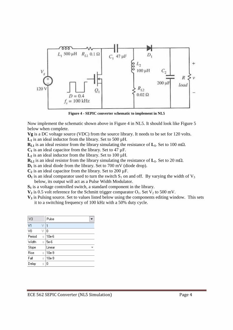
The schematic below shows the SEPIC converter with actual components substituted for the ideal switches and the resistance of non-ideal inductors added.
ECE 562 SEPIC Converter (NL5 Simulation) Page 4
Figure 4 - SEPIC converter schematic to implement in NL5
Now implement the schematic shown above in Figure 4 in NL5. It should look like Figure 5 below when complete. Vg is a DC voltage source (VDC) from the source library. It needs to be set for 120 volts. L 1 is an ideal inductor from the library. Set to 500 µH. RL1 is an ideal resistor from the library simulating the resistance of L 1. Set to 100 mΩ. C1 is an ideal capacitor from the library. Set to 47 µF. L 2 is an ideal inductor from the library. Set to 100 µH. RL2 is an ideal resistor from the library simulating the resistance of L 1. Set to 20 mΩ. D1 is an ideal diode from the library. Set to 700 mV (diode drop). C2 is an ideal capacitor from the library. Set to 200 µF. O1 is an ideal comparator used to turn the switch S1 on and off. By varying the width of V3
below, its output will act as a Pulse Width Modulator. S1 is a voltage controlled switch, a standard component in the library. V2 is 0.5 volt reference for the Schmitt trigger comparator O1. Set V2 to 500 mV. V3 is Pulsing source. Set to values listed below using the components editing window. This sets
it to a switching frequency of 100 kHz with a 50% duty cycle.
ECE 562 SEPIC Converter (NL5 Simulation) Page 5
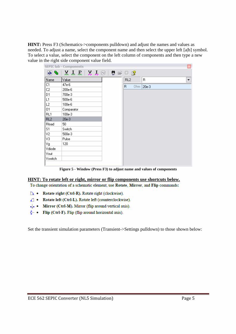
HINT: Press F3 (Schematics->components pulldown) and adjust the names and values as needed. To adjust a name, select the component name and then select the upper left [a|b] symbol. To select a value, select the component on the left column of components and then type a new value in the right side component value field.
Figure 5 - Window (Press F3) to adjust name and values of components
HINT: To rotate left or right, mirror or flip compo nents use shortcuts below.
Set the transient simulation parameters (Transient->Settings pulldown) to those shown below:

ECE 562 SEPIC Converter (NL5 Simulation) Page 6
The schematic below shows the NL5 schematic for the SEPIC converter.
Figure 6- SEPIC NL5 schematic
ECE 562 SEPIC Converter (NL5 Simulation) Page 7
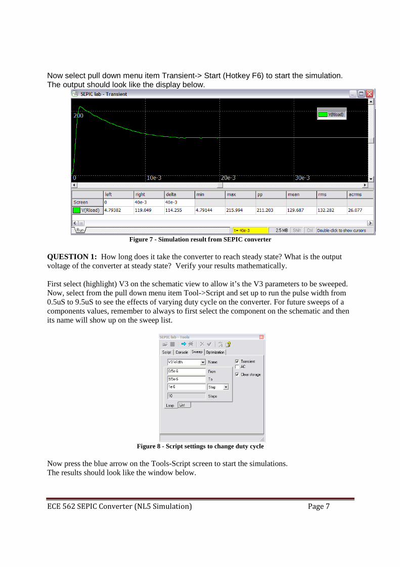
Now select pull down menu item Transient-> Start (Hotkey F6) to start the simulation. The output should look like the display below.
Figure 7 - Simulation result from SEPIC converter
QUESTION 1: How long does it take the converter to reach steady state? What is the output voltage of the converter at steady state? Verify your results mathematically. First select (highlight) V3 on the schematic view to allow it’s the V3 parameters to be sweeped. Now, select from the pull down menu item Tool->Script and set up to run the pulse width from 0.5uS to 9.5uS to see the effects of varying duty cycle on the converter. For future sweeps of a components values, remember to always to first select the component on the schematic and then its name will show up on the sweep list.
Figure 8 - Script settings to change duty cycle
Now press the blue arrow on the Tools-Script screen to start the simulations. The results should look like the window below.
ECE 562 SEPIC Converter (NL5 Simulation) Page 8
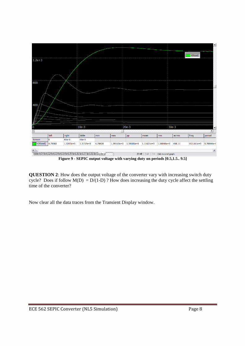
Figure 9 - SEPIC output voltage with varying duty on periods [0.5,1.5.. 9.5]
QUESTION 2: How does the output voltage of the converter vary with increasing switch duty cycle? Does if follow M(D) = D/(1-D) ? How does increasing the duty cycle affect the settling time of the converter? Now clear all the data traces from the Transient Display window.
ECE 562 SEPIC Converter (NL5 Simulation) Page 9
Hint: To clear all the traces, select Transient->Data pull down menu, select the ‘storage’ tab and click on the black middle left ‘X’ to delete all data traces from the display.
Figure 10 – Select Transient ->Data then Storage tab to get screen to clear the data
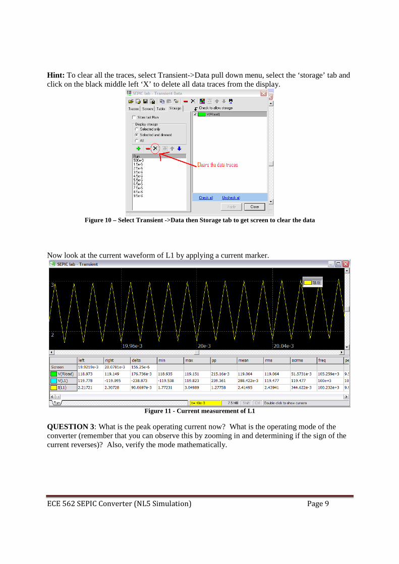
Now look at the current waveform of L1 by applying a current marker.
Figure 11 - Current measurement of L1
QUESTION 3: What is the peak operating current now? What is the operating mode of the converter (remember that you can observe this by zooming in and determining if the sign of the current reverses)? Also, verify the mode mathematically.

ECE 562 SEPIC Converter (NL5 Simulation) Page 10
Now look at the current waveform of L2 by applying a current marker.
Figure 12 - Current waveform of L2
QUESTION 4: Does the current waveform of L2 show a continuous or discontinuous mode of operation? Now place a current marker on both L1 and L2 and swept the Rload from 10 to 100 ohms using the script feature.
Figure 13 - L1 and L2 currents with Rload changes from 10 to 100 ohms in 10 ohm steps.

ECE 562 SEPIC Converter (NL5 Simulation) Page 11
QUESTION 5: Does the converter change modes of operation when the load resistance changes? If so, what is the approximate load resistance where the converter changes from one mode to the other (continuous versus discontinuous) mode? Now clear all the data and set Rload back to 50 ohms. Place a voltage marker on the output and run the transient simulation.
Figure 14 - Measurement of voltage ripple
QUESTION 6: What is the output ripple voltage of the converter? Now insert a resistor in series with C2 to simulate the capacitor’s Equivalent Series Resistance. Set the ESR resistor’s initial value to 1 ohm.
Figure 15 - SEPIC converter modified to simulate the output capacitor's ESR effects.
ECE 562 SEPIC Converter (NL5 Simulation) Page 12
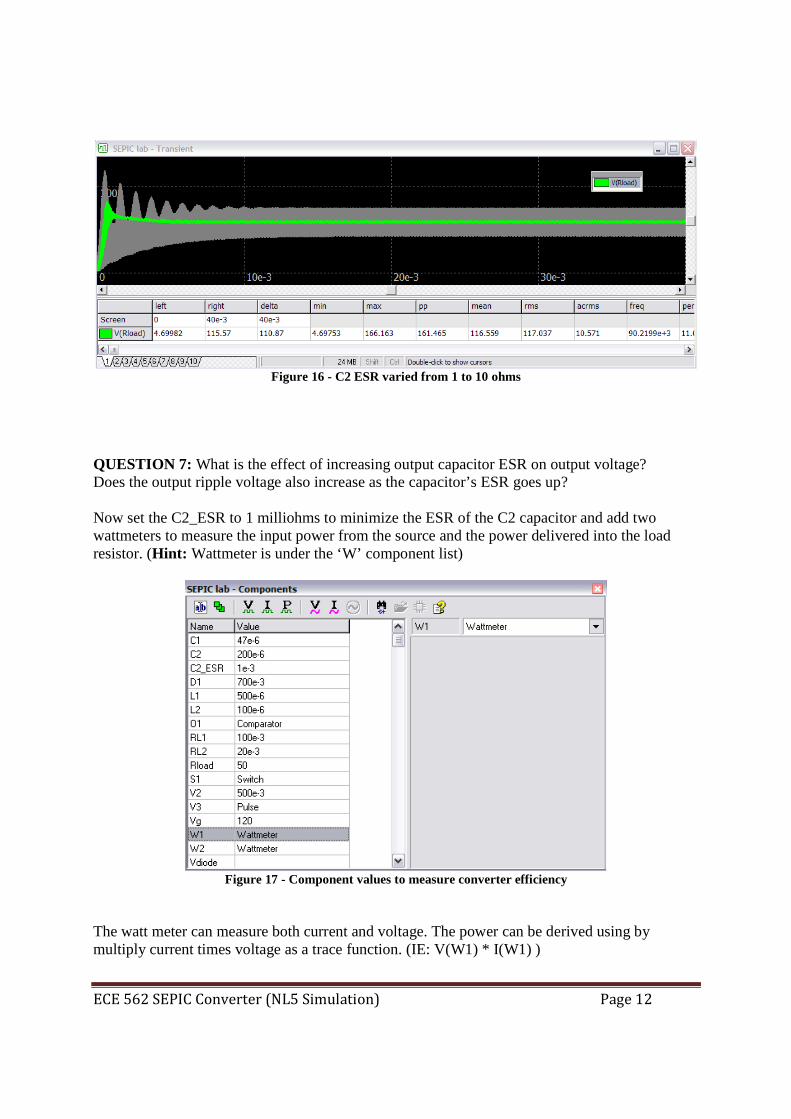
Figure 16 - C2 ESR varied from 1 to 10 ohms
QUESTION 7: What is the effect of increasing output capacitor ESR on output voltage? Does the output ripple voltage also increase as the capacitor’s ESR goes up? Now set the C2_ESR to 1 milliohms to minimize the ESR of the C2 capacitor and add two wattmeters to measure the input power from the source and the power delivered into the load resistor. (Hint: Wattmeter is under the ‘W’ component list)
Figure 17 - Component values to measure converter efficiency
The watt meter can measure both current and voltage. The power can be derived using by multiply current times voltage as a trace function. (IE: V(W1) * I(W1) )
ECE 562 SEPIC Converter (NL5 Simulation) Page 13
Figure 18 - Wattmeter description from page 383 of NL5 manual
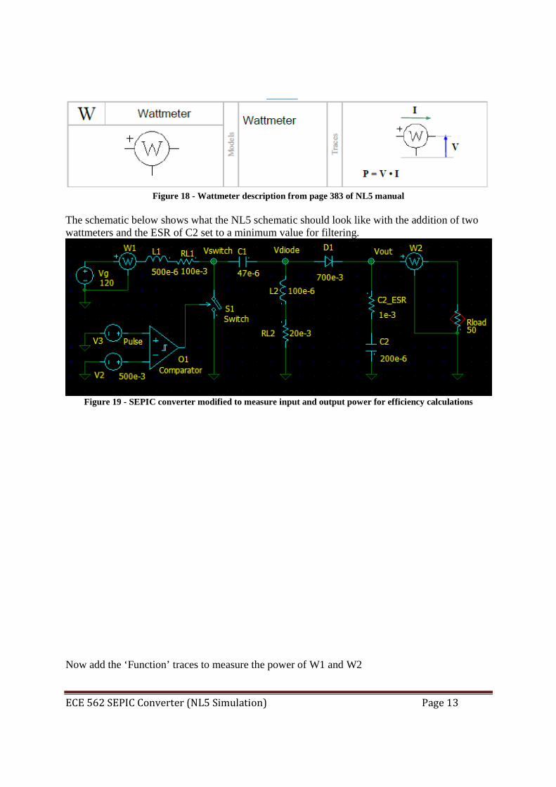
The schematic below shows what the NL5 schematic should look like with the addition of two wattmeters and the ESR of C2 set to a minimum value for filtering.
Figure 19 - SEPIC converter modified to measure input and output power for efficiency calculations
Now add the ‘Function’ traces to measure the power of W1 and W2

ECE 562 SEPIC Converter (NL5 Simulation) Page 14
Figure 20 - "Function" traces of V(W1)*I(W1) to measure power
Now run the simulation.
Figure 21 – NL5 Simulation showing the input and output power of converter
Right click on the trace screen and ‘Zoom In’ vertically and horizontally where the converter has reached steady state so that the ‘rms’ values of the power measurements can be obtained to calculate the converter’s efficiency.

ECE 562 SEPIC Converter (NL5 Simulation) Page 15
Figure 22 - Zooming in on steady state area of traces to get 'mean' value for efficiency calculations QUESTION 8: What is the converter’s efficiency at this operating point? QUESTION 9: What happens to the converter’s efficiency if the duty cycle is decreased to only 10% on time? QUESTION 10: What happens to the input source when the duty is reduced? QUESTION 11: If the duty cycle is 50% and the load decreases to 10 ohms what happens to the converter’s efficiency?
Additional Reading [1] “Fast Analytical Techniques for Electrical and Electronic Circuits”, Vatché Vorpérian, Cambridge University Press 2002. ISBN 0 521 62442 8. [2] http://www.switchingpowermagazine.com/downloads/Sepic%20Analysis.pdf
Related Documents