Sepic-Cuk Boost Based SIMO Converter Using dsPIC Microcontroller A Project report submitted in partial fulfilment of the requirements for the degree of B. Tech in Electrical Engineering By Rahita Majumder (11701615034) Adriraj Barua (11701615003) Under the supervision of Mr. Sarbojit Mukherjee Assistant Professor, Electrical Engineering Department of Electrical Engineering CANAL SOUTH ROAD, BELIAGHATA, KOLKATA – 700015, WEST BENGAL © 2019

Welcome message from author
This document is posted to help you gain knowledge. Please leave a comment to let me know what you think about it! Share it to your friends and learn new things together.
Transcript
Sepic-Cuk Boost Based SIMO Converter
Using dsPIC Microcontroller
A Project report submitted in partial fulfilment
of the requirements for the degree of B. Tech in Electrical Engineering
By
Rahita Majumder (11701615034) Adriraj Barua (11701615003)
Under the supervision of Mr. Sarbojit Mukherjee
Assistant Professor, Electrical Engineering
Department of Electrical Engineering RCC INSTITUTE OF INFORMATION TECHNOLOGY
CANAL SOUTH ROAD, BELIAGHATA, KOLKATA – 700015, WEST BENGAL
Maulana Abul Kalam Azad University of Technology (MAKAUT)
© 2019

CERTIFICATE To whom it may concern
This is to certify that the project work entitled Sepic-Cuk Boost Based SIMO Converter Using dsPIC Microcontroller is the bonafide work carried out by Rahita
Majumder(11701615034) and Adriraj Barua(11701615003), students of
B.Tech in the Dept. of Electrical Engineering, RCC Institute of Information
Technology (RCCIIT), Canal South Road, Beliaghata, Kolkata-700015, affiliated to
Maulana Abul Kalam Azad University of Technology (MAKAUT), West Bengal,
India, during the academic year 2018-19, in partial fulfillment of the
requirements for the degree of Bachelor of Technology in Electrical Engineering
and that this project has not submitted previously for the award of any other
degree, diploma and fellowship.
_____________________ ________________________
Signature of the Guide Signature of the HOD Name: Name: Designation Designation ___________________________ Signature of the External Examiner Name: Designation:

ACKNOWLEDGEMENT
Electrical Engineering, RCCIIT and to the authority of RCCIIT for providing all kinds of
infrastructural facility towards the research work.
It is my great fortune that I have got opportunity to carry out this project work under the supervision
of Assistant Prof Sarbojit Mukherjee in the Department of Electrical Engineering, RCC Institute
of Information Technology (RCCIIT), Canal South Road, Beliaghata, Kolkata-700015, affiliated to
Maulana Abul Kalam Azad University of Technology (MAKAUT), West Bengal, India. I express
my sincere thanks and deepest sense of gratitude to my guide for his constant support, unparalleled
guidance and limitless encouragement.
I wish to convey my gratitude to Associate Prof. (Dr.) Debasish Mondal, HOD, Department
of Electrical Engineering, RCCIIT and to the authority of RCCIIT for providing all kinds of
infrastructural facility towards the research work.
I would also like to convey my gratitude to all the faculty members and staffs of the Department
of Electrical Engineering, RCCIIT for their whole hearted cooperation to make this work turn into
reality.
Full Signature of the Students
Place: Date:
: Table of Contents:
List of Figures I
1. CHAPTER 1
a. INTRODUCTION 2 2. CHAPTER 2
a. THEORY 5 i. DC CONVERTER 5
ii. BUCK CONVERTER 6 iii. BOOST CONVERTER 9 iv. BUCK BOOST CONVERTER 12 v. SEPIC CONVERTER 14
vi. CUK CONVERTER 18 vii. SEPIK CUK BOOST CSC CONVERTER 22
3. CHAPTER 3 a. COMPONENT DESCRIPTION
i. RESISTOR 24 ii. INDUCTOR 25
iii. CAPACITOR 28 iv. 3 PIN PLUG 29 v. CENTER TAP TRANSFORMER 29
vi. VOLTAGE REGULATOR 30 vii. LED 31
viii. MOSFET 31 ix. TLP250 32 x. DSPIC30f4011 34
4. CHAPTER 4 a. INDUCTOR DESIGN 36
5. CHAPTER 5 a. TLP250 CIRCUIT OPERATION 40 b. POWER CIRCUIT 41 c. SNUBBER DESIGN 43
6. CHAPTER 6 a. RESULT
i. SOFTWARE RESULT 46 ii. HARDWARE RESULT 47
7. CHAPTER 7 a. CONCLUSION 50
8. CHAPTER 8 a. REFERENCES 52
ANNEXURE

LIST OF FIGURES:
Fig no. Name of Figures Page no.
1. Buck Converter 6 2. Boost Converter 10 3. Buck Boost Converter 12 4. Sepic Converter 14 5. Cuk Converter 18 6. Isolated Cuk Converter 21 7. Sepic C uk Boost CSC Converter 22 8. Resistor 25 9. Inductor 25 10. Types of Inductor 27 11. Capasitor 28 12. 3 pin Plug 29 13. Transformer 29 14. Diode 30 15. Voltage Regulator 30 16. Led 31 17. Mosfet 31 18. Cross Section of Toroidal transformer 38 19. TLP250 Working Ckt 40 20. Snubber Ckt 43 21. Waveform of Gate pulse 46 22. Waveform of Primary inductor voltage 46 23. Waveform of output voltage 46 24. Waveform of capacitor voltage 47 25. Waveform of TLP250 47 26. Waveform of MOSFET voltage 48

ABSTRACT In recent years, different techniques for multiple dc outputs and different voltage levels have been
studied and developed. This research has focused on isolated dc–dc converter configurations, such
as those for flyback, forward, pushpull, halfbridge, and fullbridge (Hbridge; this term is derived
from the typical graphical representation of such a circuit) converters, as well as nonisolated dc–dc
converters. Several applications have also been studied, such as integrated dual output converters,
integrated multipleoutput converters, and single inductor multipleoutput converters . In addition,
emerging power architectures orient ed toward renewable energy sources (such as wind turbine,
solar array, and fuel cells), batteries, and distributedgeneration utility grids have proliferated in
important ways. The concept of multiport converters applies to a static power electronic converter,
which is capable of interfacing with different sources and storage systems and with loads having
different voltage levels. Multiport converters are particularly interesting for sustainable
energygeneration systems that must integrate various lowpower sources and storage elements. A
first classification of the multiport converters can be performed as a function of the input and output
number; these include configurations for multipleinput, multipleoutput (MIMO) multipleinput,
singleoutput (MISO) , and 7USIMO converters.

CHAPTER 1
Introduction
The photovoltaic systems are major contributors in the electrical power. These are utilized
effectively with interface to the existing systems through DC-DC converters. The major challenge is
to extract power under varying operating conditions which influence the output voltage.
Isolated converter structures with cascaded configuration enables to achieve high voltage gain.
These are used up to several kW applications. The multilevel buck converters proposed are widely
used in high frequency DC/DC power conversion. In the conventional boost converters, high
voltage ratio is feasible without multistage cascading. The voltage ratios in these are limited by the
parasitic elements and switching control used.
Today, dc–dc power converters are becoming the main branch of power electronics. Recent
reports indicate that dc–dc converters represent the largest percentage of total conversion equipment
production. The worldwide dc–dc converter market has grown an average of 7.5% in recent years.
In addition to its high growth rate, the dc–dc converter market is undergoing drastic changes
because of two major trends in the electronics industry: low voltage and high power density. The
production of dc–dc converters in the world market is now much higher than that of ac–dc
converters. The divided market comprises three subsegments, including low power, medium power,
and high power.
In recent years, different techniques for multiple dc outputs and different voltage levels have
been studied and developed. Several applications have been studied, such as integrated dual-output
converters, integrated multiple-output converters, and single-inductor multiple- output converters.
Emerging power architectures oriented toward renewable energy sources batteries, and
distributed-generation utility grids have proliferated in important ways.
The concept of multiport converters applies to a static power electronic converter, which is
capable of interfacing with different sources and storage systems and with loads having different
voltage levels. Multiport converters are particularly interesting for sustainable energy-generation
systems that must integrate various low-power sources and storage elements. A first
classification of the multiport converters can be performed as a function of the input and output
number. These include configurations for multiple-input, multiple-output (MIMO) multiple-input,
single-output (MISO) and SIMO converters. SIMO dc– dc converters, in both their isolated and
nonisolated versions, have been traditionally used for multiple supplies with different output levels
in many applications, such as telecommunications, microelectronics, and lighting, that include
electronic ballast and light- emitting diodes and hybrid/electric and electric vehicles.
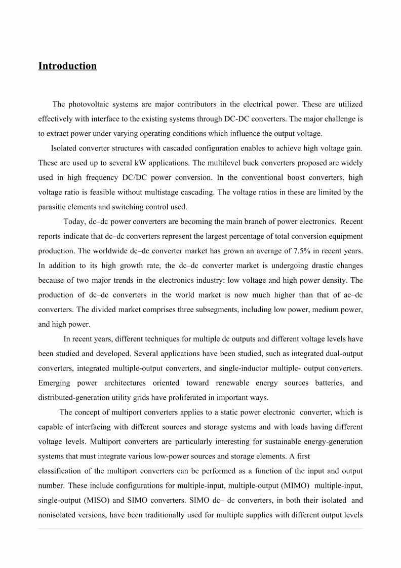
the methodology described, based on a SEPICCukboost combination converter. It has allowed the
development of a power supply bank of six different voltages
.

.
CHAPTER 2
THEORY
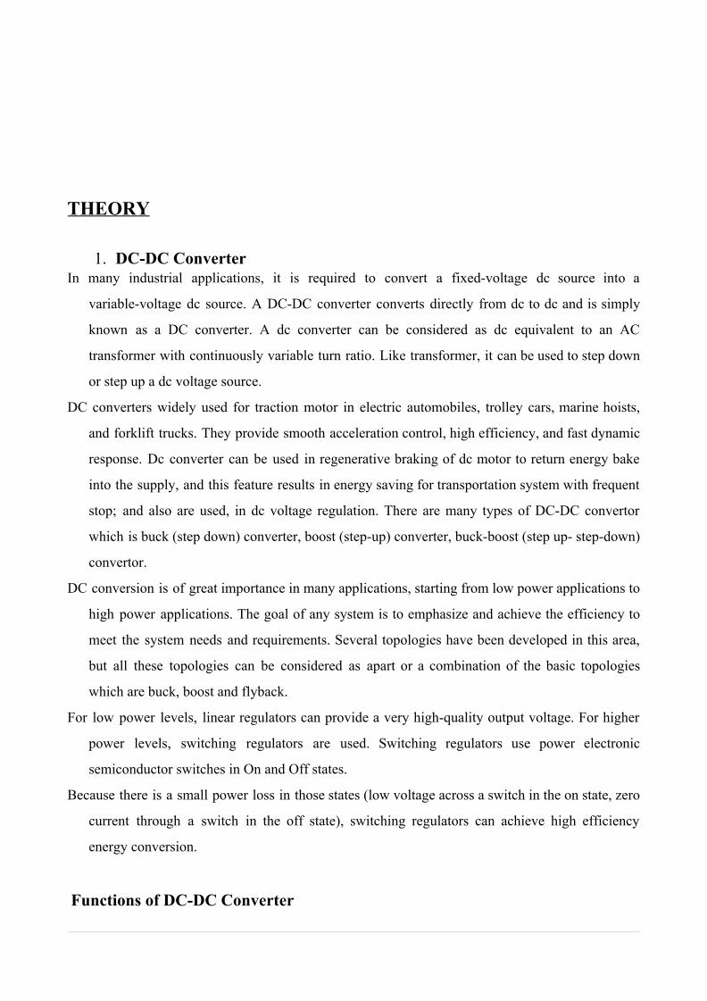
1. DC-DC Converter In many industrial applications, it is required to convert a fixed-voltage dc source into a
variable-voltage dc source. A DC-DC converter converts directly from dc to dc and is simply
known as a DC converter. A dc converter can be considered as dc equivalent to an AC
transformer with continuously variable turn ratio. Like transformer, it can be used to step down
or step up a dc voltage source.
DC converters widely used for traction motor in electric automobiles, trolley cars, marine hoists,
and forklift trucks. They provide smooth acceleration control, high efficiency, and fast dynamic
response. Dc converter can be used in regenerative braking of dc motor to return energy bake
into the supply, and this feature results in energy saving for transportation system with frequent
stop; and also are used, in dc voltage regulation. There are many types of DC-DC convertor
which is buck (step down) converter, boost (step-up) converter, buck-boost (step up- step-down)
convertor.
DC conversion is of great importance in many applications, starting from low power applications to
high power applications. The goal of any system is to emphasize and achieve the efficiency to
meet the system needs and requirements. Several topologies have been developed in this area,
but all these topologies can be considered as apart or a combination of the basic topologies
which are buck, boost and flyback.
For low power levels, linear regulators can provide a very high-quality output voltage. For higher
power levels, switching regulators are used. Switching regulators use power electronic
semiconductor switches in On and Off states.
Because there is a small power loss in those states (low voltage across a switch in the on state, zero
current through a switch in the off state), switching regulators can achieve high efficiency
energy conversion.
Functions of DC-DC Converter
The DC-DC converter has some functions. These are:
i) Convert a DC input voltage Vs into a DC output voltage Vo.
ii) Regulate the DC output voltage against load and line variations.
iii) Reduce the AC voltage ripple on the DC output voltage below the required level.
iv) Provide isolation between the input source and the load.
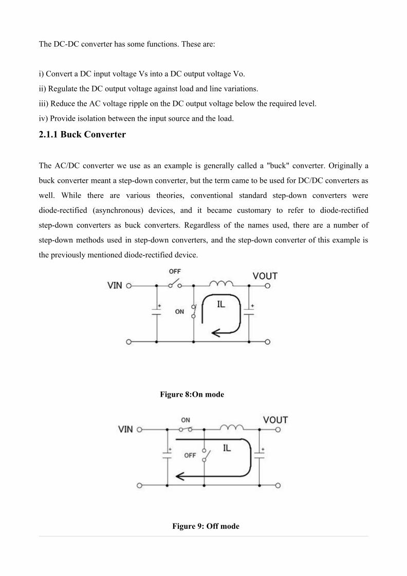
2.1.1 Buck Converter
The AC/DC converter we use as an example is generally called a "buck" converter. Originally a
buck converter meant a step-down converter, but the term came to be used for DC/DC converters as
well. While there are various theories, conventional standard step-down converters were
diode-rectified (asynchronous) devices, and it became customary to refer to diode-rectified
step-down converters as buck converters. Regardless of the names used, there are a number of
step-down methods used in step-down converters, and the step-down converter of this example is
the previously mentioned diode-rectified device.
Figure 8:On mode
Figure 9: Off mode
Operation of Buck Converters
Below, a model of a basic step-down converter is used to explain the circuit operation. By gaining
an understanding of the properties of current pathways and nodes from the basic operation,
standards for selection of peripheral components and matters demanding attention will become
clear. In the diagrams, we replace the high-side transistor and low-side diode with switches to
explain operation schematically. The circuit principles are the same as those of diode rectification in
a DC/DC converter, but the
high voltage obtained by rectifying an AC voltage is directly switched to perform step-down
voltage conversion,
and so the transistor and diode acting as switches must withstand high voltages, for example 600 V
or so.
● When the high-side switch (the transistor) turns on, a current IL flows in the inductor L, and energy
is stored
● At this time, the low-side switch (the diode) is turned off
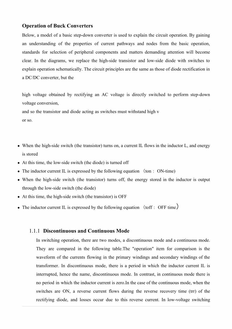
● The inductor current IL is expressed by the following equation (ton: ON-time)
● When the high-side switch (the transistor) turns off, the energy stored in the inductor is output
through the low-side switch (the diode)
● At this time, the high-side switch (the transistor) is OFF
● The inductor current IL is expressed by the following equation (toff: OFF time)
1.1.1 Discontinuous and Continuous Mode
In switching operation, there are two modes, a discontinuous mode and a continuous mode.
They are compared in the following table.The "operation" item for comparison is the
waveform of the currents flowing in the primary windings and secondary windings of the
transformer. In discontinuous mode, there is a period in which the inductor current IL is
interrupted, hence the name, discontinuous mode. In contrast, in continuous mode there is
no period in which the inductor current is zero.In the case of the continuous mode, when the
switches are ON, a reverse current flows during the reverse recovery time (trr) of the
rectifying diode, and losses occur due to this reverse current. In low-voltage switching
DC/DC conversion, the reverse voltage of the rectifying diode is low and the reverse current
is also small, and so generally the continuous mode is used, giving priority to reducing the
output ripple voltage and harmonicsHowever, the peak current becomes large, and when the
load is large, sometimes operation in continuous mode is preferred.
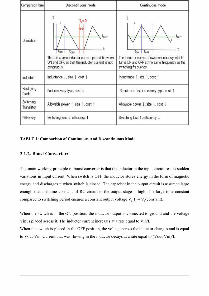
TABLE 1: Comparison of Continuous And Discontinuous Mode
2.1.2. Boost Converter:
The main working principle of boost converter is that the inductor in the input circuit resists sudden
variations in input current. When switch is OFF the inductor stores energy in the form of magnetic
energy and discharges it when switch is closed. The capacitor in the output circuit is assumed large
enough that the time constant of RC circuit in the output stage is high. The large time constant
compared to switching period ensures a constant output voltage Vo(t) = Vo(constant).
When the switch is in the ON position, the inductor output is connected to ground and the voltage
Vin is placed across it. The inductor current increases at a rate equal to Vin/L.
When the switch is placed in the OFF position, the voltage across the inductor changes and is equal
to Vout-Vin. Current that was flowing in the inductor decays at a rate equal to (Vout-Vin)/L.
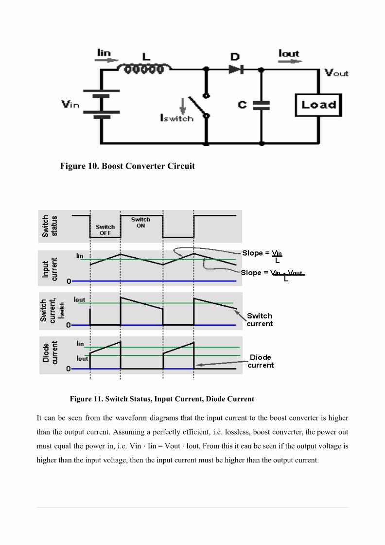
Figure 10. Boost Converter Circuit
Figure 11. Switch Status, Input Current, Diode Current
It can be seen from the waveform diagrams that the input current to the boost converter is higher
than the output current. Assuming a perfectly efficient, i.e. lossless, boost converter, the power out
must equal the power in, i.e. Vin ⋅ Iin = Vout ⋅ Iout. From this it can be seen if the output voltage is
higher than the input voltage, then the input current must be higher than the output current.
Modes of operation of Boost converter
The boost converter can be operated in two modes
a) Continuous conduction mode in which the current through inductor never goes to zero i.e.
inductor partially discharges before the start of the switching cycle.
b) Discontinuous conduction mode in which the current through inductor goes to zero i.e. inductor
is completely discharged at the end of switch.
Continuous conduction mode
case-1: When switch S is ON
When switch in ON the diode will be open circuited since the n side of diode is at higher voltage
compared to p side which is shorted to ground through the switch. During this state the inductor
charges and the inductor current increases. The current through the inductor is given as
case 2: When switch is off
When switch in OFF the diode will be short circuited and the boost converter circuit can be redrawn
as follows
The inductor now discharges through the diode and RC combination. Assume that prior to the
closing of switch the inductor current is I’’L, off. The current through the inductor is given as
Discontinuous conduction mode
The inductor in discontinuous mode drains all the current which it piled up in charging interval of
same switching cycle. The current through the inductor is given as
= (1/L)*area under the curve of voltage v/s time.
Applications of Boost converter
▪ They are used in regulated DC power supplies.
▪ They are used in regenerative braking of DC motor.
▪ Low power boost converters are used in portable device applications
▪ As switching regulator circuit in highly efficient white LED drives
▪ Boost converters are used in battery powered applications where there is space constraint to
stack more number of batteries in series to achieve higher voltages.
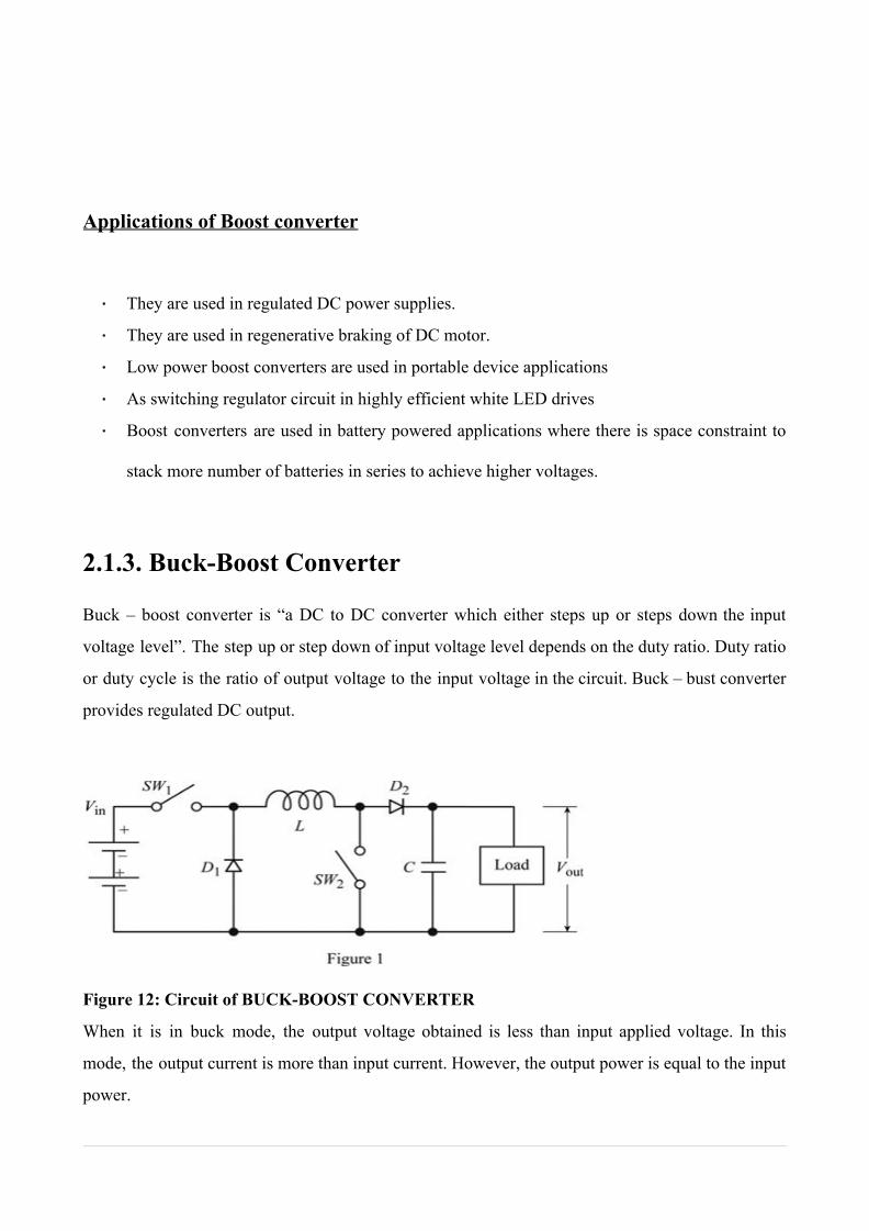
2.1.3. Buck-Boost Converter
Buck – boost converter is “a DC to DC converter which either steps up or steps down the input
voltage level”. The step up or step down of input voltage level depends on the duty ratio. Duty ratio
or duty cycle is the ratio of output voltage to the input voltage in the circuit. Buck – bust converter
provides regulated DC output.
Figure 12: Circuit of BUCK-BOOST CONVERTER
When it is in buck mode, the output voltage obtained is less than input applied voltage. In this
mode, the output current is more than input current. However, the output power is equal to the input
power.
When it is in boost mode, the output voltage obtained is more than the input applied voltage. In this
mode, the output current is less than input current. However, the output power is equal to the input
power.
To operate the buck – boost converter, the two switches will operate simultaneously. When
switches are closed, inductor stores energy in a magnetic field. When switches are open, the
inductors get discharged and give the supply to the load. The inductors in the circuit do not allow
sudden variations in the current. The capacitor across the load provides a regulated DC output.
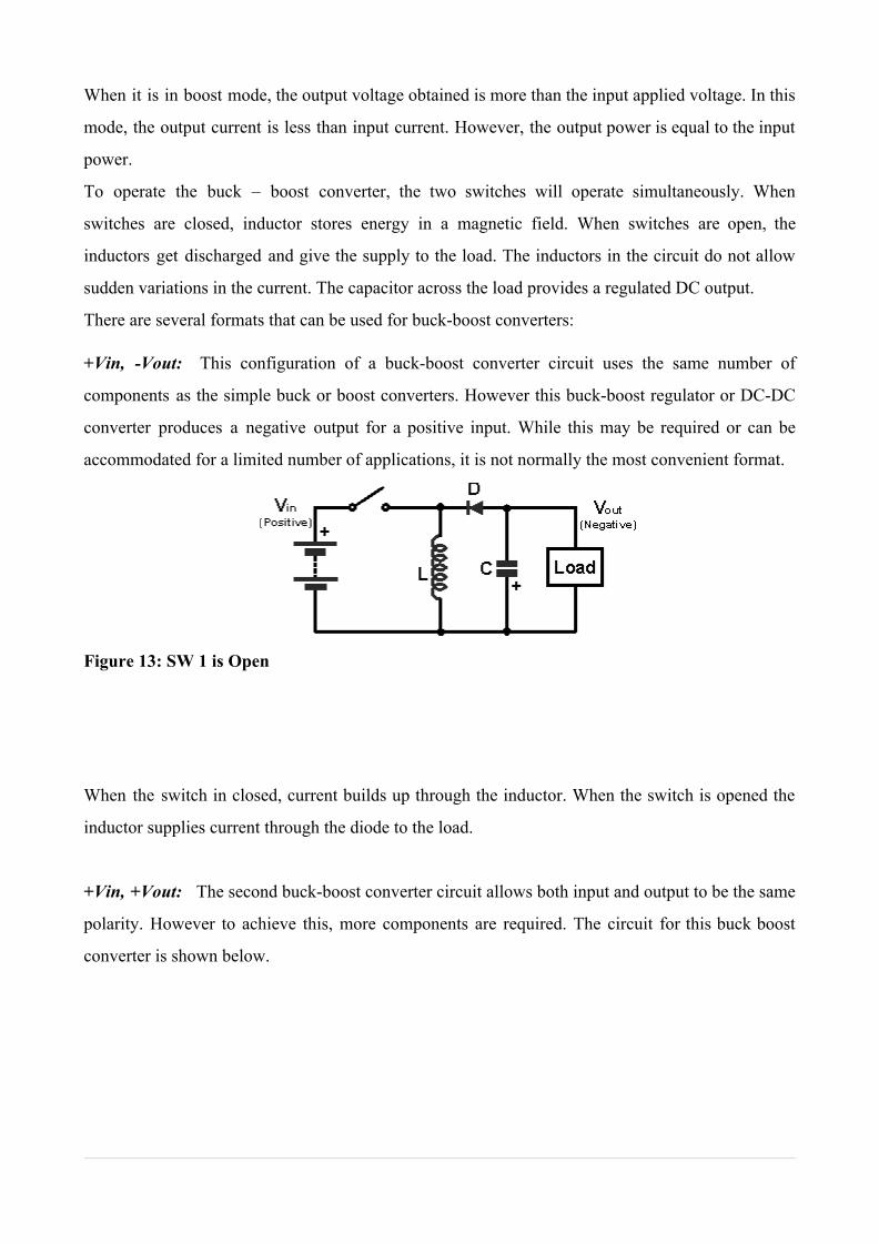
There are several formats that can be used for buck-boost converters:
+Vin, -Vout: This configuration of a buck-boost converter circuit uses the same number of
components as the simple buck or boost converters. However this buck-boost regulator or DC-DC
converter produces a negative output for a positive input. While this may be required or can be
accommodated for a limited number of applications, it is not normally the most convenient format.
Figure 13: SW 1 is Open
When the switch in closed, current builds up through the inductor. When the switch is opened the
inductor supplies current through the diode to the load.
+Vin, +Vout: The second buck-boost converter circuit allows both input and output to be the same
polarity. However to achieve this, more components are required. The circuit for this buck boost
converter is shown below.
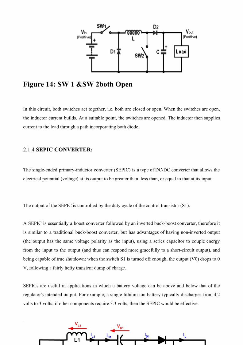
Figure 14: SW 1 &SW 2both Open
In this circuit, both switches act together, i.e. both are closed or open. When the switches are open,
the inductor current builds. At a suitable point, the switches are opened. The inductor then supplies
current to the load through a path incorporating both diode.
2.1.4 SEPIC CONVERTER:
The single-ended primary-inductor converter (SEPIC) is a type of DC/DC converter that allows the
electrical potential (voltage) at its output to be greater than, less than, or equal to that at its input.
The output of the SEPIC is controlled by the duty cycle of the control transistor (S1).
A SEPIC is essentially a boost converter followed by an inverted buck-boost converter, therefore it
is similar to a traditional buck-boost converter, but has advantages of having non-inverted output
(the output has the same voltage polarity as the input), using a series capacitor to couple energy
from the input to the output (and thus can respond more gracefully to a short-circuit output), and
being capable of true shutdown: when the switch S1 is turned off enough, the output (V0) drops to 0
V, following a fairly hefty transient dump of charge.
SEPICs are useful in applications in which a battery voltage can be above and below that of the
regulator's intended output. For example, a single lithium ion battery typically discharges from 4.2
volts to 3 volts; if other components require 3.3 volts, then the SEPIC would be effective.
Circuit operation
The schematic diagram for a basic SEPIC is shown in Figure 1. As with other switched mode power
supplies (specifically DC-to-DC converters), the SEPIC exchanges energy between the capacitors
and inductors in order to convert from one voltage to another. The amount of energy exchanged is
controlled by switch S1, which is typically a transistor such as a MOSFET. MOSFETs offer much
higher input impedance and lower voltage drop than bipolar junction transistors (BJTs), and do not
require biasing resistors as MOSFET switching is controlled by differences in voltage rather than a
current, as with BJTs.
Continuous mode
A SEPIC is said to be in continuous-conduction mode ("continuous mode") if the current through
the inductor L1 never falls to zero. During a SEPIC's steady-state operation, the average voltage
across capacitor C1 (VC1) is equal to the input voltage (Vin). Because capacitor C1 blocks direct
current (DC), the average current through it (IC1) is zero, making inductor L2 the only source of
DC load current. Therefore, the average current through inductor L2 (IL2) is the same as the
average load current and hence independent of the input voltage.
Looking at average voltages, the following can be written:
VIN=VL1+VC1+VL2
Because the average voltage of VC1 is equal to VIN, VL1 = −VL2. For this reason, the two
inductors can be wound on the same core. Since the voltages are the same in magnitude, their
effects of the mutual inductance will be zero, assuming the polarity of the windings is correct. Also,
since the voltages are the same in magnitude, the ripple currents from the two inductors will be
equal in magnitude.
The average currents can be summed as follows (average capacitor currents must be
zero):ID1=IL1-IL2
When switch S1 is turned on, current IL1 increases and the current IL2 goes more negative.
(Mathematically, it decreases due to arrow direction.) The energy to increase the current IL1 comes
from the input source. Since S1 is a short while closed, and the instantaneous voltage VL1 is
approximately VIN, the voltage VL2 is approximately −VC1. Therefore, D1 is opened and the
capacitor C1 supplies the energy to increase the magnitude of the current in IL2 and thus increase
the energy stored in L2. IL is supplied by C2. The easiest way to visualize this is to consider the bias
voltages of the circuit in a d.c. state, then close S1.
Figure 2: With S1 closed current increases through L1 (green) and C1
discharges increasing current in L2 (red)
When switch S1 is turned off, the current IC1 becomes the same as the current IL1, since inductors
do not allow instantaneous changes in current. The current IL2 will continue in the negative
direction, in fact it never reverses direction. It can be seen from the diagram that a negative IL2 will
add to the current IL1 to increase the current delivered to the load. Using Kirchhoff's Current Law,
it can be shown that ID1 = IC1 - IL2. It can then be concluded, that while S1 is off, power is
delivered to the load from both L2 and L1. C1, however is being charged by L1 during this off
cycle (as C2 by L1 and L2), and will in turn recharge L2 during the following on cycle.
Figure 3: With S1 open current through L1 (green) and current through L2
(red) produce current through the load Because the potential (voltage) across capacitor C1 may reverse direction every cycle, a
non-polarized capacitor should be used. However, a polarized tantalum or electrolytic capacitor
may be used in some cases,[2] because the potential (voltage) across capacitor C1 will not change
unless the switch is closed long enough for a half cycle of resonance with inductor L2, and by this
time the current in inductor L1 could be quite large.
The capacitor CIN is required to reduce the effects of the parasitic inductance and internal
resistance of the power supply. The boost/buck capabilities of the SEPIC are possible because of
capacitor C1 and inductor L2. Inductor L1 and switch S1 create a standard boost converter, which
generates a voltage (VS1) that is higher than VIN, whose magnitude is determined by the duty cycle
of the switch S1. Since the average voltage across C1 is VIN, the output voltage (VO) is VS1 -
VIN. If VS1 is less than double VIN, then the output voltage will be less than the input voltage. If
VS1 is greater than double VIN, then the output voltage will be greater than the input voltage.
The evolution of switched-power supplies can be seen by coupling the two inductors in a SEPIC
converter together, which begins to resemble a Flyback converter, the most basic of the
transformer-isolated SMPS topologies.
Discontinuous mode
A SEPIC is said to be in discontinuous-conduction mode or discontinuous mode if the current
through the inductor L2 is allowed to fall to zero. Reliability and efficiency
The voltage drop and switching time of diode D1 is critical to a SEPIC's reliability and efficiency.
The diode's switching time needs to be extremely fast in order to not generate high voltage spikes
across the inductors, which could cause damage to components. Fast conventional diodes or
Schottky diodes may be used.
The resistances in the inductors and the capacitors can also have large effects on the converter
efficiency and output ripple. Inductors with lower series resistance allow less energy to be
dissipated as heat, resulting in greater efficiency (a larger portion of the input power being
transferred to the load). Capacitors with low equivalent series resistance (ESR) should also be used
for C1 and C2 to minimize ripple and prevent heat build-up, especially in C1 where the current is
changing direction frequently.
Disadvantages
Like the buck–boost converter, the SEPIC has a pulsating output current. The similar Ćuk converter
does not have this disadvantage, but it can only have negative output polarity, unless the isolated
Ćuk converter is used.
Since the SEPIC converter transfers all its energy via the series capacitor, a capacitor with high
capacitance and current handling capability is required.
The fourth-order nature of the converter also makes the SEPIC converter difficult to control,
making it only suitable for very slow varying applications.
CUK CONVERTER:
The Ćuk converter (pronounced chook; sometimes incorrectly spelled Cuk, Čuk or Cúk) is a type
of DC/DC converter that has an output voltage magnitude that is either greater than or less than the
input voltage magnitude. It is essentially a boost converter followed by a buck converter with a
capacitor to couple the energy.
Similar to the buck–boost converter with inverting topology, the output voltage of non-isolated Ćuk
is typically also inverting, and can be lower or higher than the input. It uses a capacitor as its main
energy-storage component, unlike most other types of converters which use an inductor. It is named
after Slobodan Ćuk of the California Institute of Technology, who first presented the design.
Operating principle
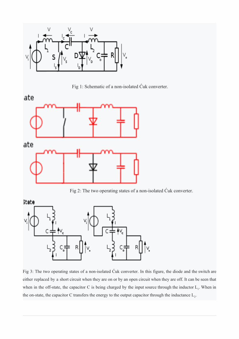
Fig 1: Schematic of a non-isolated Ćuk converter.
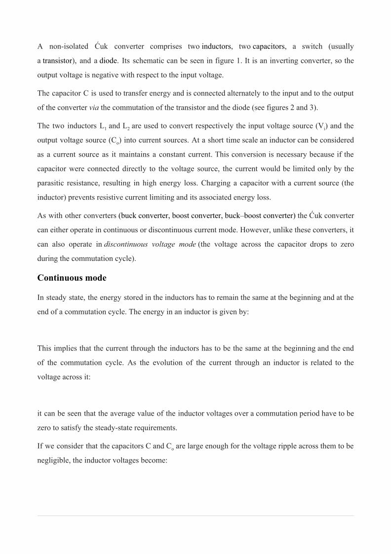
Fig 2: The two operating states of a non-isolated Ćuk converter.
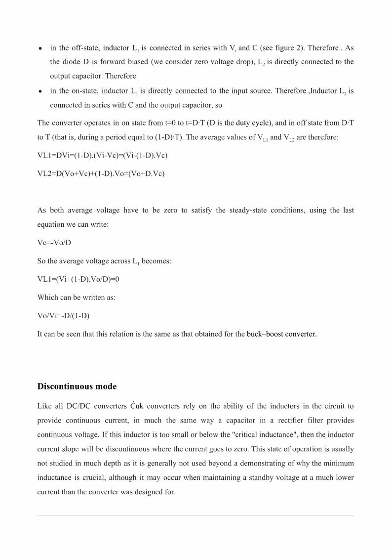
Fig 3: The two operating states of a non-isolated Ćuk converter. In this figure, the diode and the switch are
either replaced by a short circuit when they are on or by an open circuit when they are off. It can be seen that
when in the off-state, the capacitor C is being charged by the input source through the inductor L1. When in
the on-state, the capacitor C transfers the energy to the output capacitor through the inductance L2.
A non-isolated Ćuk converter comprises two inductors, two capacitors, a switch (usually
a transistor), and a diode. Its schematic can be seen in figure 1. It is an inverting converter, so the
output voltage is negative with respect to the input voltage.
The capacitor C is used to transfer energy and is connected alternately to the input and to the output
of the converter via the commutation of the transistor and the diode (see figures 2 and 3).
The two inductors L1 and L2 are used to convert respectively the input voltage source (Vi) and the
output voltage source (Co) into current sources. At a short time scale an inductor can be considered
as a current source as it maintains a constant current. This conversion is necessary because if the
capacitor were connected directly to the voltage source, the current would be limited only by the
parasitic resistance, resulting in high energy loss. Charging a capacitor with a current source (the
inductor) prevents resistive current limiting and its associated energy loss.
As with other converters (buck converter, boost converter, buck–boost converter) the Ćuk converter
can either operate in continuous or discontinuous current mode. However, unlike these converters, it
can also operate in discontinuous voltage mode (the voltage across the capacitor drops to zero
during the commutation cycle).
Continuous mode
In steady state, the energy stored in the inductors has to remain the same at the beginning and at the
end of a commutation cycle. The energy in an inductor is given by:
This implies that the current through the inductors has to be the same at the beginning and the end
of the commutation cycle. As the evolution of the current through an inductor is related to the
voltage across it:
it can be seen that the average value of the inductor voltages over a commutation period have to be
zero to satisfy the steady-state requirements.
If we consider that the capacitors C and Co are large enough for the voltage ripple across them to be
negligible, the inductor voltages become:
● in the off-state, inductor L1 is connected in series with Vi and C (see figure 2). Therefore . As
the diode D is forward biased (we consider zero voltage drop), L2 is directly connected to the
output capacitor. Therefore
● in the on-state, inductor L1 is directly connected to the input source. Therefore ,Inductor L2 is
connected in series with C and the output capacitor, so
The converter operates in on state from t=0 to t=D·T (D is the duty cycle), and in off state from D·T
to T (that is, during a period equal to (1-D)·T). The average values of VL1 and VL2 are therefore:
VL1=DVi=(1-D).(Vi-Vc)=(Vi-(1-D).Vc)
VL2=D(Vo+Vc)+(1-D).Vo=(Vo+D.Vc)
As both average voltage have to be zero to satisfy the steady-state conditions, using the last
equation we can write:
Vc=-Vo/D
So the average voltage across L1 becomes:
VL1=(Vi+(1-D).Vo/D)=0
Which can be written as:
Vo/Vi=-D/(1-D)
It can be seen that this relation is the same as that obtained for the buck–boost converter.
Discontinuous mode
Like all DC/DC converters Ćuk converters rely on the ability of the inductors in the circuit to
provide continuous current, in much the same way a capacitor in a rectifier filter provides
continuous voltage. If this inductor is too small or below the "critical inductance", then the inductor
current slope will be discontinuous where the current goes to zero. This state of operation is usually
not studied in much depth as it is generally not used beyond a demonstrating of why the minimum
inductance is crucial, although it may occur when maintaining a standby voltage at a much lower
current than the converter was designed for.
The minimum inductance is given by:
L1min=(1-D)^2.R/2Dfs
Where fs is the switching frequency.
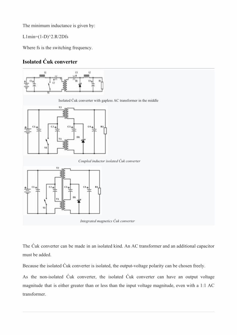
Isolated Ćuk converter
Isolated Ćuk converter with gapless AC transformer in the middle
Coupled inductor isolated Ćuk converter
Integrated magnetics Ćuk converter
The Ćuk converter can be made in an isolated kind. An AC transformer and an additional capacitor
must be added.
Because the isolated Ćuk converter is isolated, the output-voltage polarity can be chosen freely.
As the non-isolated Ćuk converter, the isolated Ćuk converter can have an output voltage
magnitude that is either greater than or less than the input voltage magnitude, even with a 1:1 AC
transformer.
Related structures
Inductor coupling
Instead of using two discrete inductor components, many designers implement a coupled inductor
Ćuk converter, using a single magnetic component that includes both inductors on the same core.
The transformer action between the inductors inside that component gives a coupled inductor Ćuk
converter with lower output ripple than a Ćuk converter using two independent discrete inductor
components.
Zeta Converter
A zeta converter provides an ouput voltage that is the opposite of the output voltage of a Ćuk
converter.
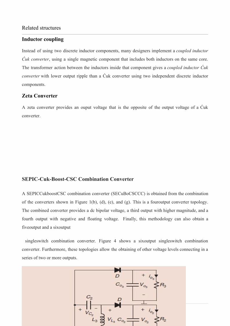
SEPIC-Cuk-Boost-CSC Combination Converter
A SEPICCukboostCSC combination converter (SECuBoCSCCC) is obtained from the combination
of the converters shown in Figure 1(b), (d), (e), and (g). This is a fouroutput converter topology.
The combined converter provides a dc bipolar voltage, a third output with higher magnitude, and a
fourth output with negative and floating voltage. Finally, this methodology can also obtain a
fiveoutput and a sixoutput
singleswitch combination converter. Figure 4 shows a sixoutput singleswitch combination
converter. Furthermore, these topologies allow the obtaining of other voltage levels connecting in a
series of two or more outputs.


CHAPTER 3
COMPONENT DESCRIPTION
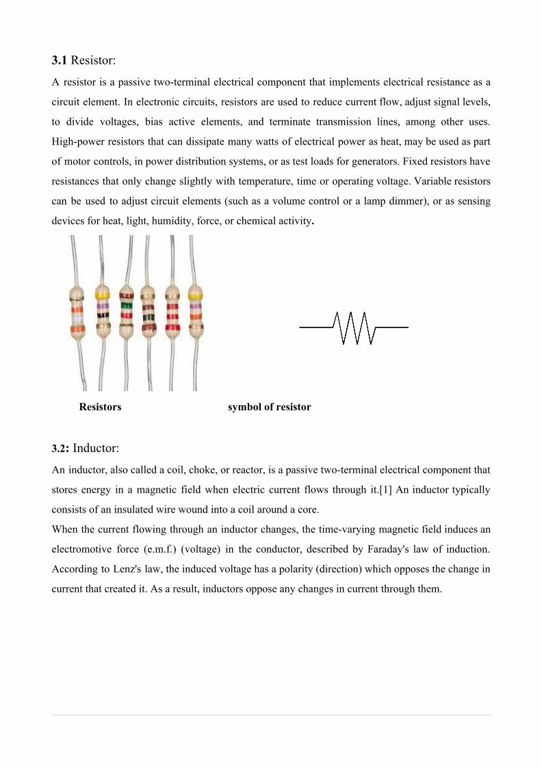
3.1 Resistor:
A resistor is a passive two-terminal electrical component that implements electrical resistance as a
circuit element. In electronic circuits, resistors are used to reduce current flow, adjust signal levels,
to divide voltages, bias active elements, and terminate transmission lines, among other uses.
High-power resistors that can dissipate many watts of electrical power as heat, may be used as part
of motor controls, in power distribution systems, or as test loads for generators. Fixed resistors have
resistances that only change slightly with temperature, time or operating voltage. Variable resistors
can be used to adjust circuit elements (such as a volume control or a lamp dimmer), or as sensing
devices for heat, light, humidity, force, or chemical activity.
Resistors symbol of resistor
3.2: Inductor:
An inductor, also called a coil, choke, or reactor, is a passive two-terminal electrical component that
stores energy in a magnetic field when electric current flows through it.[1] An inductor typically
consists of an insulated wire wound into a coil around a core.
When the current flowing through an inductor changes, the time-varying magnetic field induces an
electromotive force (e.m.f.) (voltage) in the conductor, described by Faraday's law of induction.
According to Lenz's law, the induced voltage has a polarity (direction) which opposes the change in
current that created it. As a result, inductors oppose any changes in current through them.
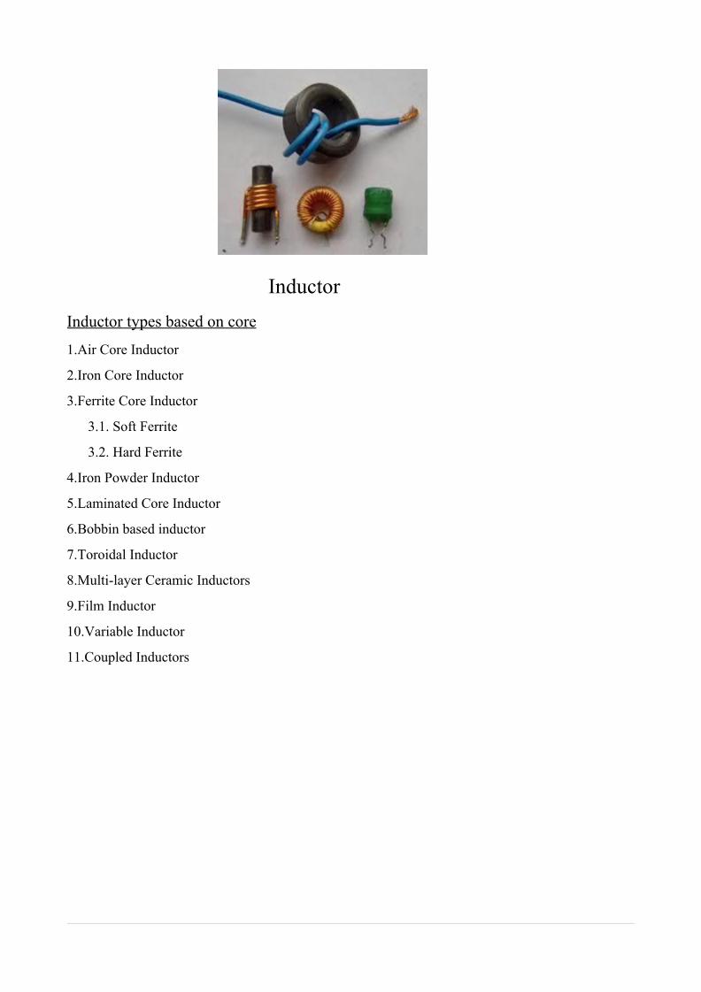
Inductor Inductor types based on core
1.Air Core Inductor
2.Iron Core Inductor
3.Ferrite Core Inductor
3.1. Soft Ferrite
3.2. Hard Ferrite
4.Iron Powder Inductor
5.Laminated Core Inductor
6.Bobbin based inductor
7.Toroidal Inductor
8.Multi-layer Ceramic Inductors
9.Film Inductor
10.Variable Inductor
11.Coupled Inductors
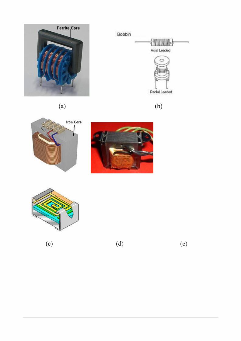
(a) (b)
(c) (d) (e)
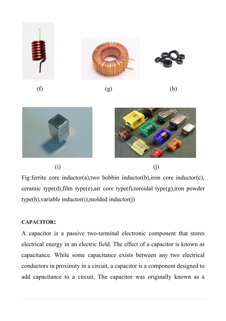
(f) (g) (h)
(i) (j)
Fig:ferrite core inductor(a),two bobbin inductor(b),iron core inductor(c),
ceramic type(d),film type(e),air core type(f),toroidal type(g),iron powder
type(h),variable inductor(i),molded inductor(j)
CAPACITOR:
A capacitor is a passive two-terminal electronic component that stores
electrical energy in an electric field. The effect of a capacitor is known as
capacitance. While some capacitance exists between any two electrical
conductors in proximity in a circuit, a capacitor is a component designed to
add capacitance to a circuit. The capacitor was originally known as a
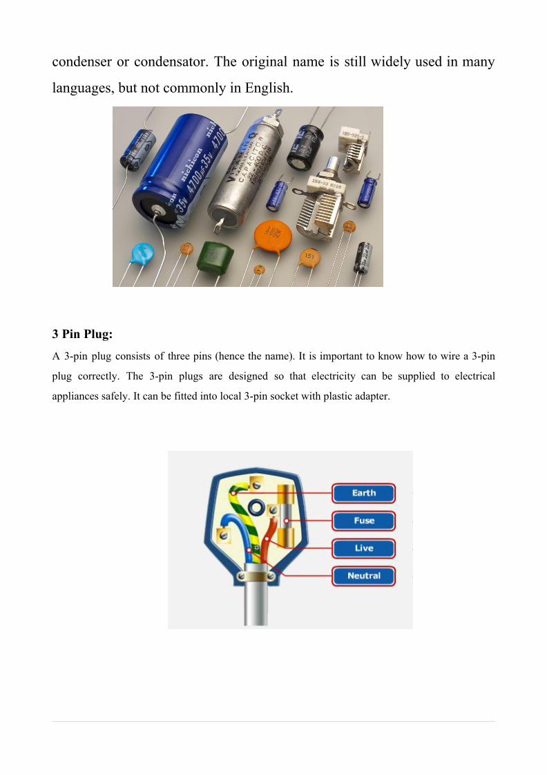
condenser or condensator. The original name is still widely used in many
languages, but not commonly in English.
3 Pin Plug:
A 3-pin plug consists of three pins (hence the name). It is important to know how to wire a 3-pin
plug correctly. The 3-pin plugs are designed so that electricity can be supplied to electrical
appliances safely. It can be fitted into local 3-pin socket with plastic adapter.
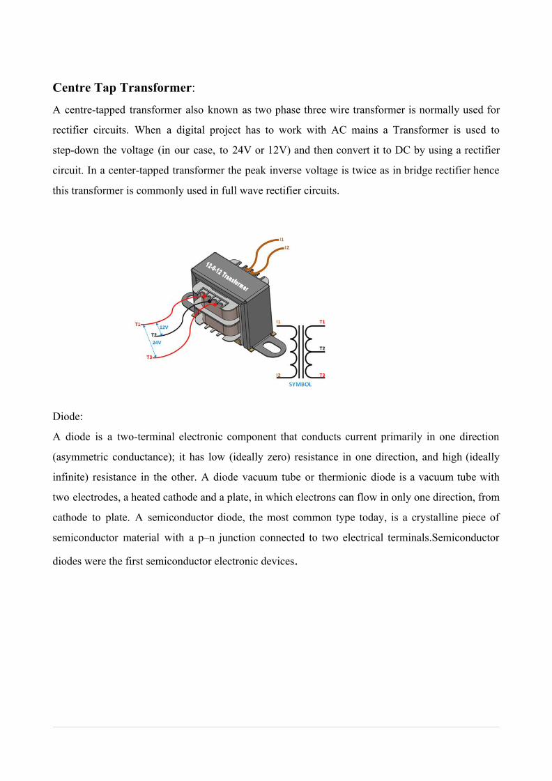
Centre Tap Transformer:
A centre-tapped transformer also known as two phase three wire transformer is normally used for
rectifier circuits. When a digital project has to work with AC mains a Transformer is used to
step-down the voltage (in our case, to 24V or 12V) and then convert it to DC by using a rectifier
circuit. In a center-tapped transformer the peak inverse voltage is twice as in bridge rectifier hence
this transformer is commonly used in full wave rectifier circuits.
Diode:
A diode is a two-terminal electronic component that conducts current primarily in one direction
(asymmetric conductance); it has low (ideally zero) resistance in one direction, and high (ideally
infinite) resistance in the other. A diode vacuum tube or thermionic diode is a vacuum tube with
two electrodes, a heated cathode and a plate, in which electrons can flow in only one direction, from
cathode to plate. A semiconductor diode, the most common type today, is a crystalline piece of
semiconductor material with a p–n junction connected to two electrical terminals.Semiconductor
diodes were the first semiconductor electronic devices.
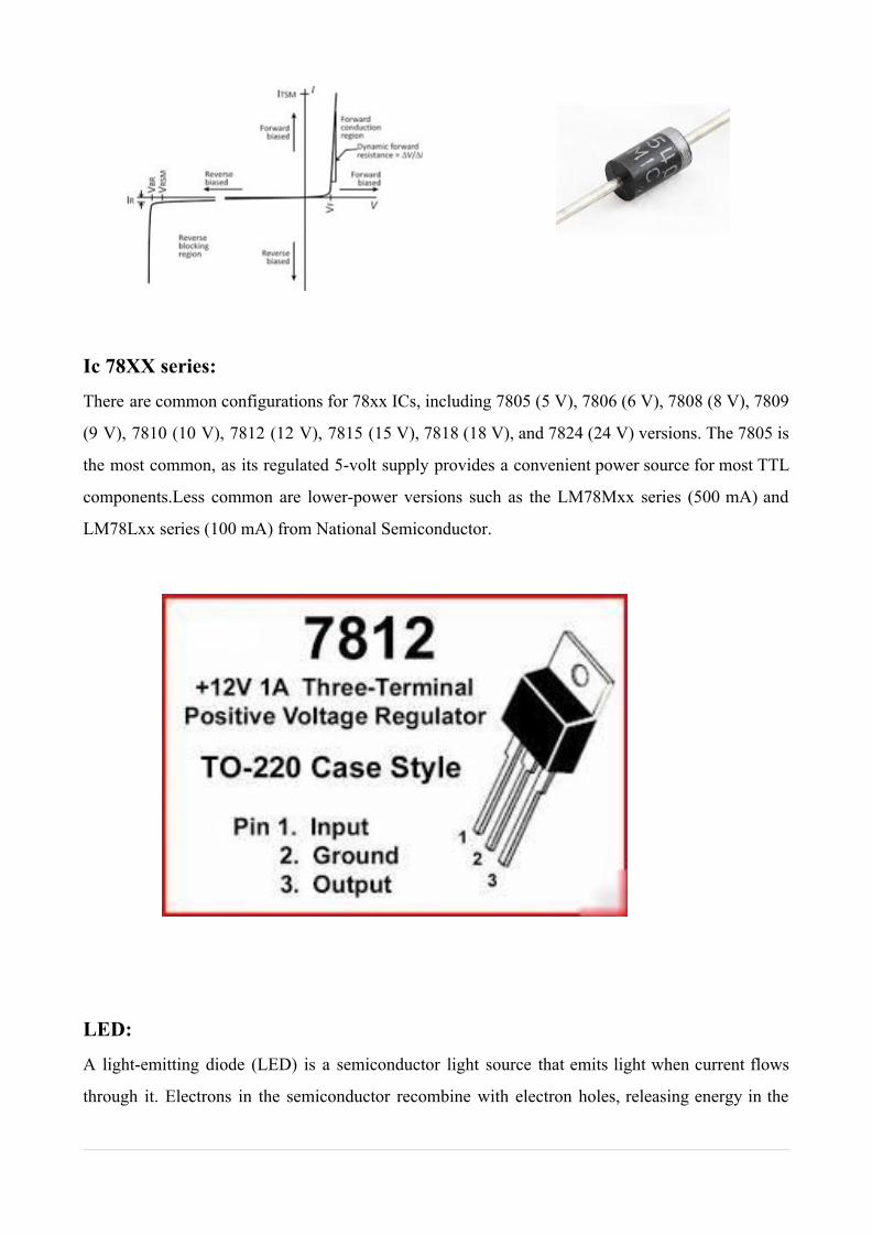
Ic 78XX series:
There are common configurations for 78xx ICs, including 7805 (5 V), 7806 (6 V), 7808 (8 V), 7809
(9 V), 7810 (10 V), 7812 (12 V), 7815 (15 V), 7818 (18 V), and 7824 (24 V) versions. The 7805 is
the most common, as its regulated 5-volt supply provides a convenient power source for most TTL
components.Less common are lower-power versions such as the LM78Mxx series (500 mA) and
LM78Lxx series (100 mA) from National Semiconductor.
LED:
A light-emitting diode (LED) is a semiconductor light source that emits light when current flows
through it. Electrons in the semiconductor recombine with electron holes, releasing energy in the
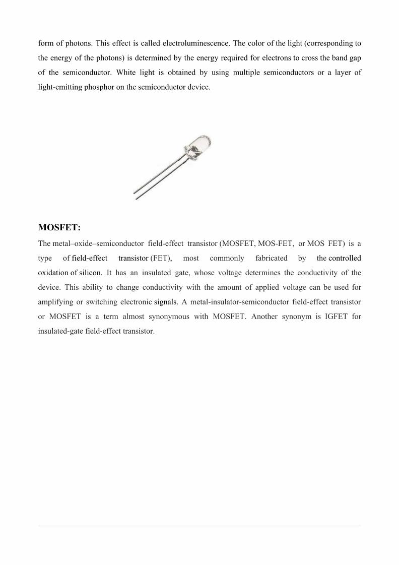
form of photons. This effect is called electroluminescence. The color of the light (corresponding to
the energy of the photons) is determined by the energy required for electrons to cross the band gap
of the semiconductor. White light is obtained by using multiple semiconductors or a layer of
light-emitting phosphor on the semiconductor device.
MOSFET:
The metal–oxide–semiconductor field-effect transistor (MOSFET, MOS-FET, or MOS FET) is a
type of field-effect transistor (FET), most commonly fabricated by the controlled
oxidation of silicon. It has an insulated gate, whose voltage determines the conductivity of the
device. This ability to change conductivity with the amount of applied voltage can be used for
amplifying or switching electronic signals. A metal-insulator-semiconductor field-effect transistor
or MOSFET is a term almost synonymous with MOSFET. Another synonym is IGFET for
insulated-gate field-effect transistor.
TLP250:
The TOSHIBA TLP250 consists of a GaAlAs light emitting diode and a
integrated photodetector.This unit is 8-lead DIP package.TLP250 is suitable for gate driving circuit
of IGBT or power MOS FET.
schematic:
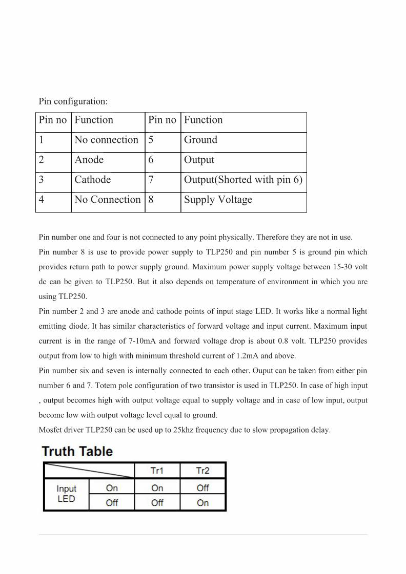
Pin configuration:
Pin no Function Pin no Function
1 No connection 5 Ground
2 Anode 6 Output
3 Cathode 7 Output(Shorted with pin 6)
4 No Connection 8 Supply Voltage
Pin number one and four is not connected to any point physically. Therefore they are not in use.
Pin number 8 is use to provide power supply to TLP250 and pin number 5 is ground pin which
provides return path to power supply ground. Maximum power supply voltage between 15-30 volt
dc can be given to TLP250. But it also depends on temperature of environment in which you are
using TLP250.
Pin number 2 and 3 are anode and cathode points of input stage LED. It works like a normal light
emitting diode. It has similar characteristics of forward voltage and input current. Maximum input
current is in the range of 7-10mA and forward voltage drop is about 0.8 volt. TLP250 provides
output from low to high with minimum threshold current of 1.2mA and above.
Pin number six and seven is internally connected to each other. Ouput can be taken from either pin
number 6 and 7. Totem pole configuration of two transistor is used in TLP250. In case of high input
, output becomes high with output voltage equal to supply voltage and in case of low input, output
become low with output voltage level equal to ground.
Mosfet driver TLP250 can be used up to 25khz frequency due to slow propagation delay.
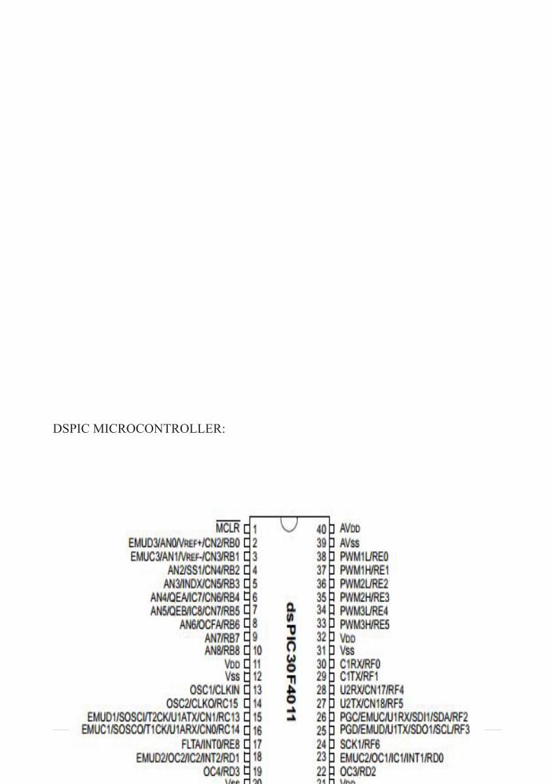
DSPIC MICROCONTROLLER:

High Performance Modified RISC CPU: • Modified Harvard architecture • C compiler optimized instruction set architecture with flexible addressing modes • 84 base instructions • 24-bit wide instructions, 16-bit wide data path • 48 Kbytes on-chip Flash program space (16K Instruction words) • 2 Kbytes of on-chip data RAM • 1 Kbytes of non-volatile data EEPROM • Up to 30 MIPs operation: - DC to 40 MHz external clock input - 4 MHz-10 MHz oscillator input with PLL active (4x, 8x, 16x) • 30 interrupt sources - 3 external interrupt sources - 8 user selectable priority levels for each interrupt source - 4 processor trap sources • 16 x 16-bit working register array DSP Engine Features: • Dual data fetch • Accumulator write back for DSP operations • Modulo and Bit-Reversed Addressing modes • Two, 40-bit wide accumulators with optional saturation logic • 17-bit x 17-bit single cycle hardware fractional/ integer multiplier • All DSP instructions single cycle • ± 16-bit single cycle shift
Peripheral Features: • High current sink/source I/O pins: 25 mA/25 mA • Timer module with programmable prescaler: - Five 16-bit timers/counters; optionally pair 16-bit timers into 32-bit timer modules • 16-bit Capture input functions • 16-bit Compare/PWM output functions • 3-wire SPI™ modules (supports 4 Frame modes) • I2C™ module supports Multi-Master/Slave mode and 7-bit/10-bit addressing • 2 UART modules with FIFO Buffers • 1 CAN modules, 2.0B compliant
Motor Control PWM Module Features: • 6 PWM output channels - Complementary or Independent Output modes - Edge and Center Aligned modes

• 3 duty cycle generators • Dedicated time base • Programmable output polarity • Dead-time control for Complementary mode • Manual output control • Trigger for A/D conversions Quadrature Encoder Interface Module Features: • Phase A, Phase B and Index Pulse input • 16-bit up/down position counter • Count direction status • Position Measurement (x2 and x4) mode • Programmable digital noise filters on inputs • Alternate 16-bit Timer/Counter mode • Interrupt on position counter rollover/underflow
CHAPTER 4
INDUCTOR DESIGN The design of an ac inductor is quite similar to that of a transformer. If there is no dc flux in the
core, the design calculations are straightforward. The apparent power, Pt , of an inductor is the VA
of the inductor; that is, the product of the excitation voltage and the current through the inductor.
The design of the ac inductor requires the calculation of the volt-amp (VA) capability. In some
applications the inductance is specified, and in others, the current is specified. If the inductance is
specified, then, the current has to be calculated. If the current is specified, then the inductance has to
be calculated.
The design of a linear ac inductor depends upon five related factors:
1. Desired inductance
2. Applied voltage, (across inductor)
3.Frequency
4. Operating Flux density
5.Temperature Rise
Cores of Inductor:
An electric current through a wire wound into a coil creates a magnetic field through the center of
the coil, due to Ampere's circuital law. Coils are widely used in electronic components such as
electromagnets, inductors, transformers, electric motors and generators. A coil without a magnetic
core is called an "air core" coil. Adding a piece of ferromagnetic or ferrimagnetic material in the
center of the coil can increase the magnetic field by hundreds or thousands of times; this is called a
magnetic core. The field of the wire penetrates the core material, magnetizing it, so that the strong
magnetic field of the core adds to the field created by the wire. The amount that the magnetic field
is increased by the core depends on the magnetic permeability of the core material. Because side
effects such as eddy currents and hysteresis can cause frequency-dependent energy losses, different
core materials are used for coils used at different frequencies.
The cores can be of different types. Some of them are:
1.Single "I" core
Like a cylindrical rod but square, rarely used on its own. This type of core is most likely to be found
in car ignition coils.
2."C" or "U" core
U and C-shaped cores are used with I or another C or U core to make a square closed core, the
simplest closed core shape. Windings may be put on one or both legs of the core.
3."E" core
E-shaped core are more symmetric solutions to form a closed magnetic system. Most of the time,
the electric circuit is wound around the center leg, whose section area is twice that of each
individual outer leg. In 3-phase transformer cores, the legs are of equal size, and all three legs are
wound.
4.Pair of "E" cores
Again used for iron cores. Similar to using an "E" and "I" together, a pair of "E" cores will
accommodate a larger coil former and can produce a larger inductor or transformer. If an air gap is
required, the centre leg of the "E" is shortened so that the air gap sits in the middle of the coil to
minimize fringing and reduce electromagnetic interference.
5.Planar core
A planar core consists of two flat pieces of magnetic material, one above and one below the coil. It
is typically used with a flat coil that is part of a printed circuit board. This design is excellent for
mass production and allows a high power, small volume transformer to be constructed for low cost.
It is not as ideal as either a pot core or toroidal core [citation needed] but costs less to produce.
6.Pot Core
Usually ferrite or similar. This is used for inductors and transformers. The shape of a pot core is
round with an internal hollow that almost completely encloses the coil. Usually a pot core is made
in two halves which fit together around a coil former (bobbin). This design of core has a shielding
effect, preventing radiation and reducing electromagnetic interference.
7.Ring or bead
The ring is essentially identical in shape and performance to the toroid, except that inductors
commonly pass only through the center of the core, without wrapping around the core multiple
times.
The ring core may also be composed of two separate C-shaped hemispheres secured together within
a plastic shell, permitting it to be placed on finished cables with large connectors already installed,
that would prevent threading the cable through the small inner diameter of a solid ring.
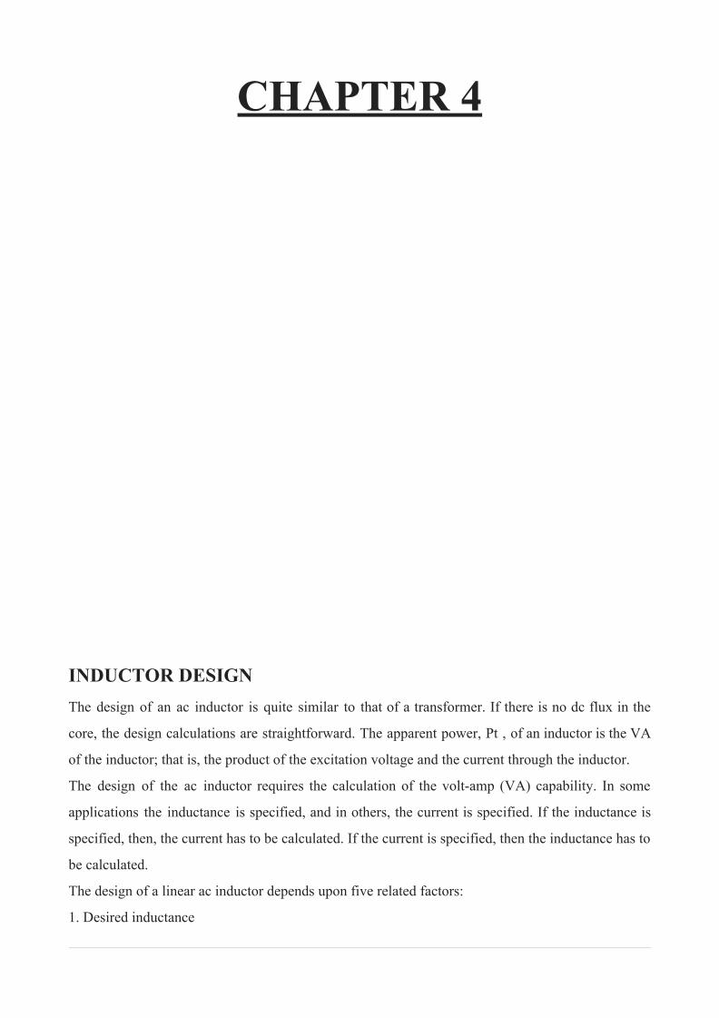
8.Toroidal Cores.
There are many different types
of magnetic material used for
fabricating inductors. The
purpose of the material is to
provide permittivity greater
than µO so that the inductors
can be made more compactly
and with fewer turns of wire.
This can reduce skin effect
losses in the wire and reduce coupling to other inductive components in the circuit, but the circuit
losses then may be limited by the magnetic material itself. There are charts of typical unloaded Q’s
that can be obtained from various materials.
For this project we have used the toroidal cores for the designing of inductors .As it is easily
available and due to its easy access and easy to turn the coils around it. Hence, toroidal cores are
being used for the designing purpose in our project.
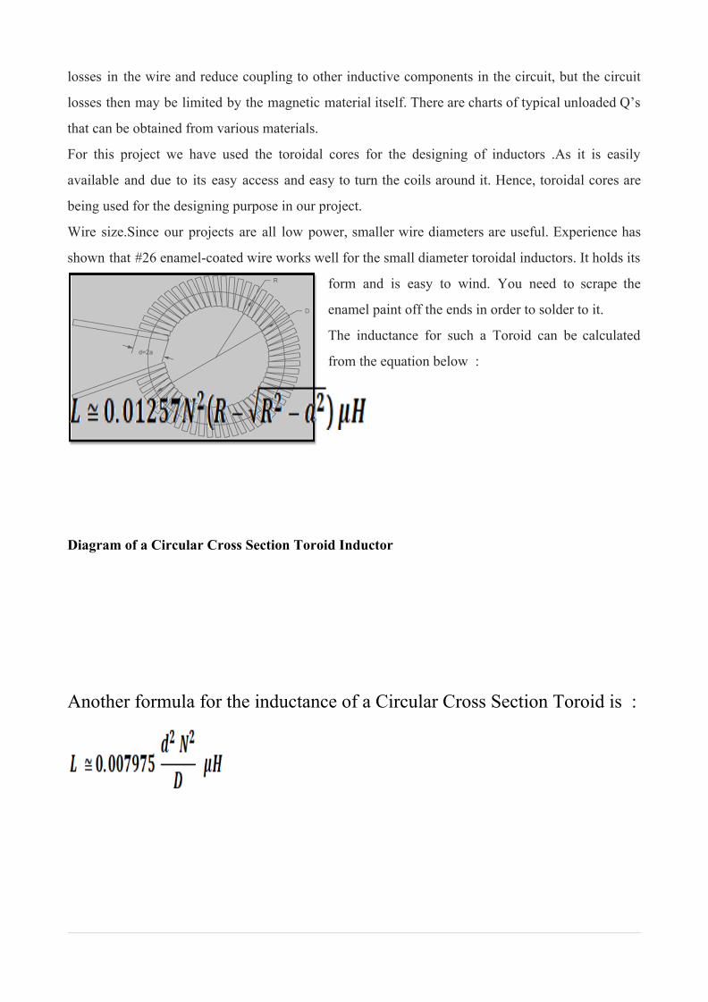
Wire size.Since our projects are all low power, smaller wire diameters are useful. Experience has
shown that #26 enamel-coated wire works well for the small diameter toroidal inductors. It holds its
form and is easy to wind. You need to scrape the
enamel paint off the ends in order to solder to it.
The inductance for such a Toroid can be calculated
from the equation below :
Diagram of a Circular Cross Section Toroid Inductor
Another formula for the inductance of a Circular Cross Section Toroid is :

Chapter 5
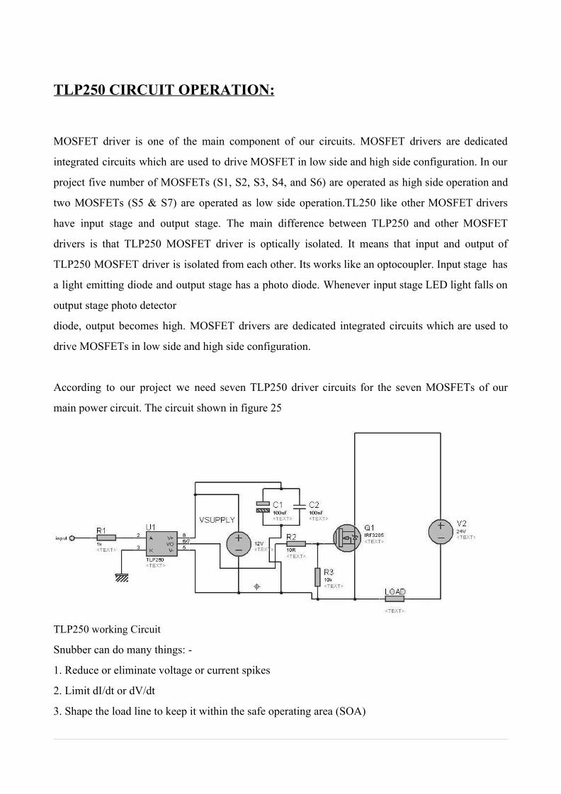
TLP250 CIRCUIT OPERATION:
MOSFET driver is one of the main component of our circuits. MOSFET drivers are dedicated
integrated circuits which are used to drive MOSFET in low side and high side configuration. In our
project five number of MOSFETs (S1, S2, S3, S4, and S6) are operated as high side operation and
two MOSFETs (S5 & S7) are operated as low side operation.TL250 like other MOSFET drivers
have input stage and output stage. The main difference between TLP250 and other MOSFET
drivers is that TLP250 MOSFET driver is optically isolated. It means that input and output of
TLP250 MOSFET driver is isolated from each other. Its works like an optocoupler. Input stage has
a light emitting diode and output stage has a photo diode. Whenever input stage LED light falls on
output stage photo detector
diode, output becomes high. MOSFET drivers are dedicated integrated circuits which are used to
drive MOSFETs in low side and high side configuration.
According to our project we need seven TLP250 driver circuits for the seven MOSFETs of our
main power circuit. The circuit shown in figure 25
TLP250 working Circuit
Snubber can do many things: -
1. Reduce or eliminate voltage or current spikes
2. Limit dI/dt or dV/dt
3. Shape the load line to keep it within the safe operating area (SOA)
4. Transfer power dissipation from the switch to a resistor or a useful load
5. Reduce total losses due to switching
POWER CIRCUIT: This can be achieved in simple three steps:
1. Firstly, 220V AC is converted into 12V AC by using simple step-down (220V/12V) transformer.
2. Secondly, output of this transformer is given to the rectifier circuit, which will convert the ac
supply into dc supply. The output of the rectifier circuit that is DC contains the ripples in the output
voltage. To filter out these ripples, capacitor of 2200 uf, 25V is used.
3. Lastly, the output of the capacitor that is pure DC is given to voltage regulator IC 7812 and
IC7912 which will regulate the output voltage at 12V and -12V DC, despite the change in input
voltage.
Required Components:
1. Centre tapped transformer (220V/12V)
2. Power Diodes (6A) – 4No.
3. Capacitor (2200μF, 25V) – 2No.
4. Voltage regulator (IC 7812 & 7912)
5. Toggle switch
6. DC load (DC motor)
Step-I: Converting 220v AC into 12v AC using Step Down Transformer
The primary terminals of the centre tapped transformer is connected with household supply (220V
ac, 50Hz) and output is taken from secondary terminals of the transformer. The centre tapped
describes the voltage output of a center tapped transformer. For example: A 24V centre tapped
transformer will measure 24V ac across the outer two taps (winding as a whole), and 12V ac from
each outer tap to the center-tap (half winding). These two 12V ac supplies are 180 degrees out of
phase with each other, thus making it easy to derive positive and negative 12 volt dc power supplies
from them. The advantage of using a centre tapped transformer is we can get the both +12V and
-12V dc supply using only one transformer.
Step – II: Converting 12v AC into 12v DC using Full Bridge Rectifier
The outer two terminals of the centre tapped transformer are connected to the bridge rectifier
circuit. Rectifier circuit is a converter, which converts ac supply in to dc supply. It is generally
made up of diode switches as shown in Circuit Diagram.
To convert ac into dc, we can make two types of rectifiers, one is half bridge rectifier and second is
full bridge rectifier. In half bridge rectifier, output voltage is half of the input voltage. For example,
if input voltage is 24V, then output dc voltage is 12V and number of diode used in this type of
rectifier is 2. In full bridge rectifier, number of diodes is 4 and it is connected as shown in figure
and output voltage is same as the input voltage.
Here, full bridge rectifier is used. So, number of diodes are 4 and input voltage (24V ac) and output
voltage is also 24V dc with ripples in it.
For, full bridge rectifier output voltage,
VDC = 2Vm / Π where, Vm=peak value of ac supply voltage and Π is Pi
Step-III: Filter the Ripples from the output:
Now, 24V dc output which contains peak to peak ripples can’t be connected directly to the load. So,
to remove ripples from the supply, filter capacitors are used. Now, two filter capacitor of rating
2200uF and 25 V are used as shown in circuit diagram. The connection of both capacitors are such
that the common terminal of the capacitors is connected directly to the centre terminal of the centre
tapped transformer. Now, this capacitor will get charged upto 12V dc as both are connected with the
common terminal of a transformer. Furthermore, the capacitors will remove the ripples from the dc
supply and give a pure dc output. But, the output of both the capacitors are not regulated. So, to
make the supply regulated, output of the capacitors are given to the voltage regulator ICs which is
explained in next step.
Step-IV: Regulate the 12v DC Power Supply
The next important thing is to regulate the output voltage of the capacitors which will otherwise be
varying as per the input voltage change. For that depending upon the output voltage requirement,
regulator ICs are used. If we need the output voltage +12V then IC 7812 is used. If required output
voltage is +5V, then 7805 IC is used. Last two digits of the IC gives output voltage rating. Third last
digit shows voltage is positive or negative. For positive voltage (8) and for negative voltage (9)
number is used. So IC7812 is used for +12v regulation and IC7912 is used for -12v voltage
regulation.
Now connection of two ICs are done as shown in circuit diagram. The ground terminal of both ICs
are connected with the centre tap terminal of the transformer in order to create a reference. Now, the
output voltages are measured between the output terminal and ground terminal for both ICs.
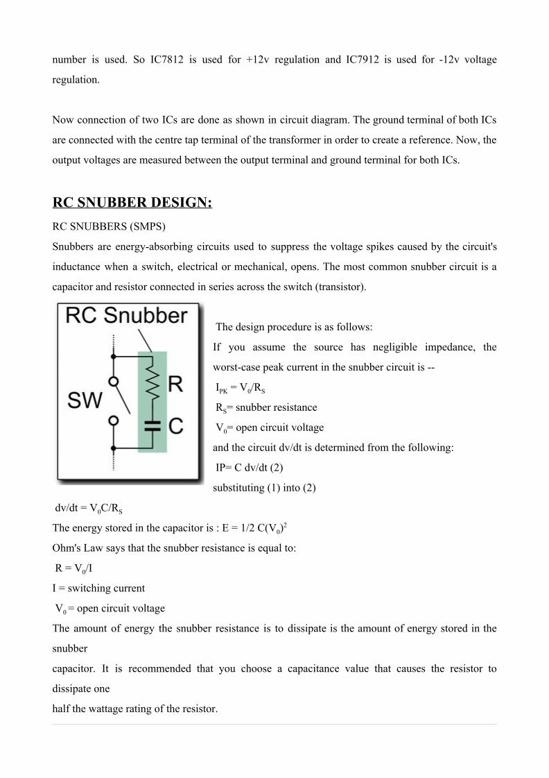
RC SNUBBER DESIGN: RC SNUBBERS (SMPS)
Snubbers are energy-absorbing circuits used to suppress the voltage spikes caused by the circuit's
inductance when a switch, electrical or mechanical, opens. The most common snubber circuit is a
capacitor and resistor connected in series across the switch (transistor).
The design procedure is as follows:
If you assume the source has negligible impedance, the
worst-case peak current in the snubber circuit is --
IPK = V0/RS
RS= snubber resistance
V0= open circuit voltage
and the circuit dv/dt is determined from the following:
IP= C dv/dt (2)
substituting (1) into (2)
dv/dt = V0C/RS
The energy stored in the capacitor is : E = 1/2 C(V0)2
Ohm's Law says that the snubber resistance is equal to:
R = V0/I
I = switching current
V0 = open circuit voltage
The amount of energy the snubber resistance is to dissipate is the amount of energy stored in the
snubber
capacitor. It is recommended that you choose a capacitance value that causes the resistor to
dissipate one
half the wattage rating of the resistor.
P = 1/2 C(V0)22f Where f = switching frequency
= C(V0)2f 2f = number of transitions per cycle
C = P/f(V0)2
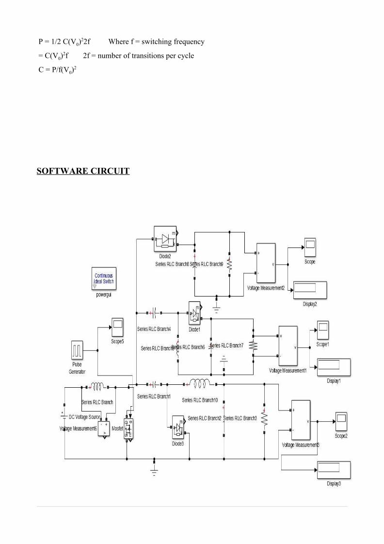
SOFTWARE CIRCUIT
Hardware Circuit
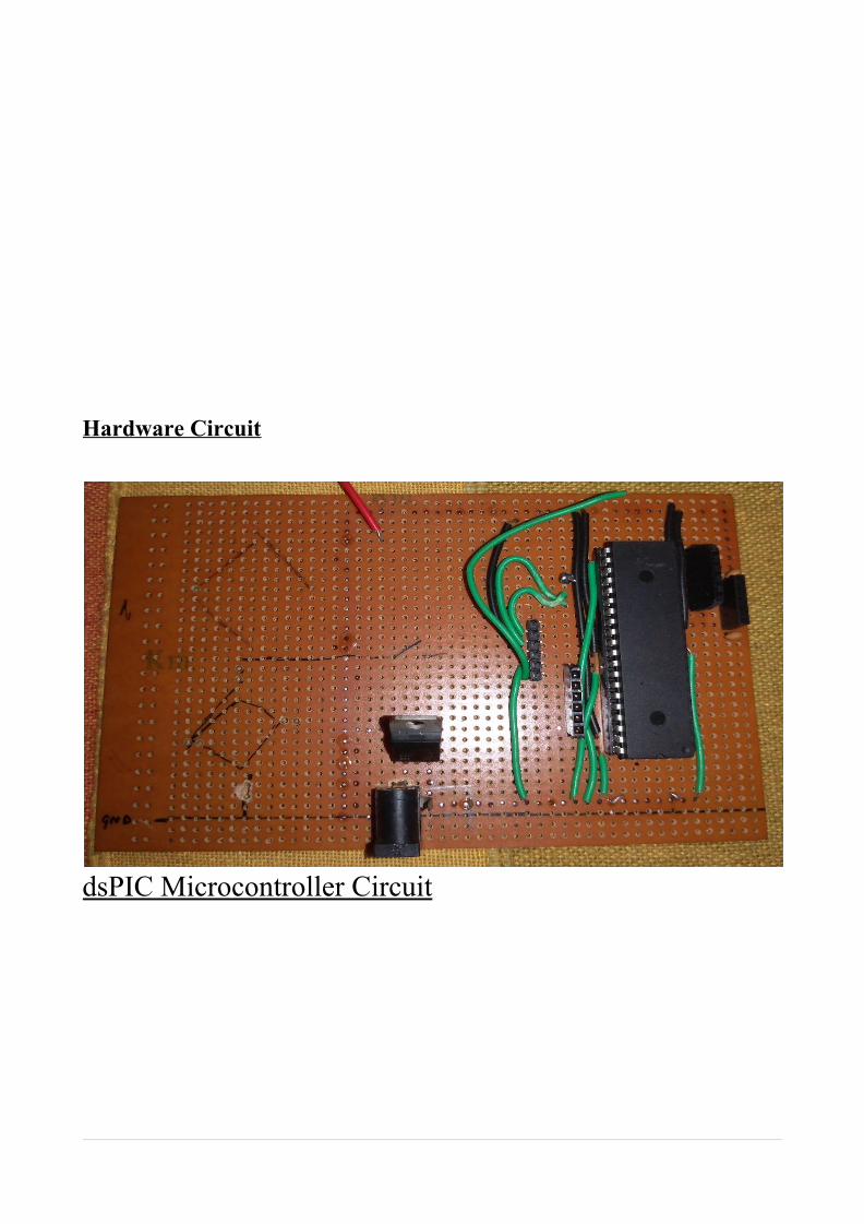
dsPIC Microcontroller Circuit
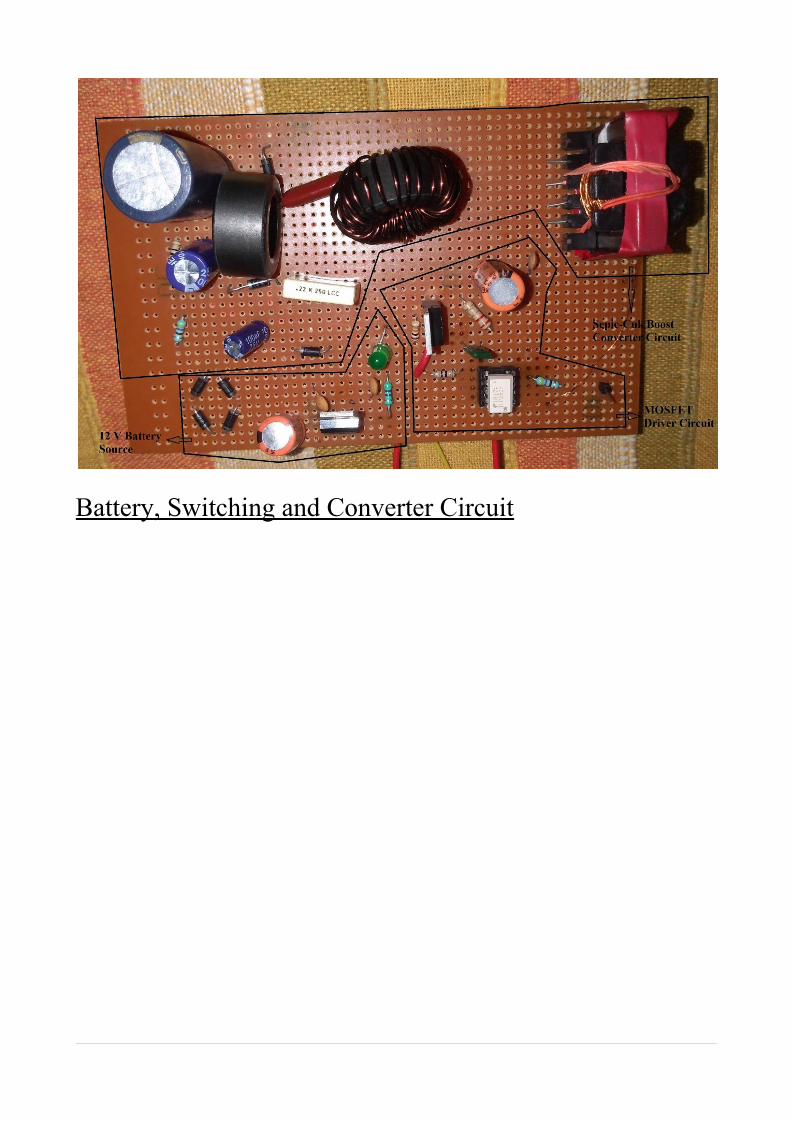
Battery, Switching and Converter Circuit

CHAPTER 6
Results
Software Waveforms:-
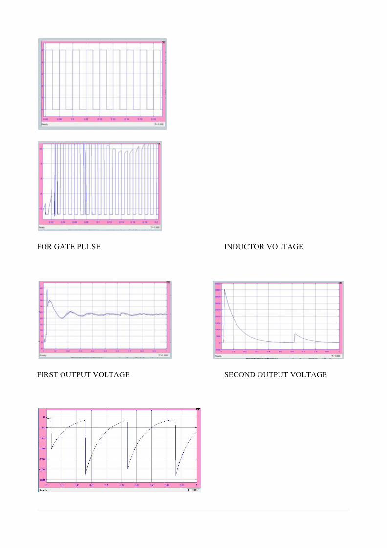
FOR GATE PULSE INDUCTOR VOLTAGE
FIRST OUTPUT VOLTAGE SECOND OUTPUT VOLTAGE

THIRD OUTPUT VOLTAGE
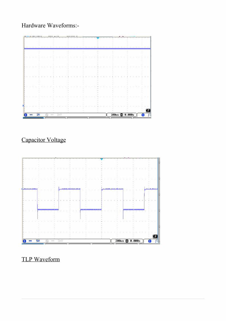
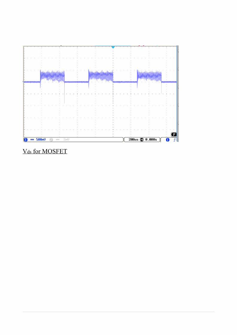
Hardware Waveforms:-
Capacitor Voltage
TLP Waveform
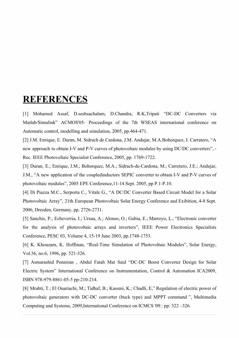
Vds for MOSFET

CHAPTER 7

RESULT ANALYSIS ● The voltage across capacitor is 2V
● Voltage at TLP input is 10V
● Drain to Source Voltage for MOSFET is 1V
Here we want to generate pulse of 2kHZ from Rdo pin of dsPIC. But due to operation delay we are
getting pulse of 1.87kHz. But this can be adjusted to 2kHz by NOP operation . We are MPLAB
X-16 compiler.
CONCLUSION A dsPIC processor has been programmed to generate the trigger pulses for the power switch in a
SEPIC buck/boost converter and function as a PI/SM controller. The implementation of the
designed control algorithm has been found to offer very good time response performance and
acceptable power quality, in addition to regulating the output voltage. The results having
demonstrated the suitability of the proposed approach for use in critical applications, will go a long
way in enhancing the scope of such converters.

CHAPTER 8
REFERENCES [1] Mohamed Assaf, D.seshsachalam, D.Chandra, R.K,Tripati “DC-DC Converters via
Matlab/Simulink” ACMOS'05- Proceedings of the 7th WSEAS international conference on
Automatic control, modelling and simulation, 2005, pp.464-471.
[2] J.M. Enrique, E. Duran, M. Sidrach de Cardona, J.M. Andujar, M.A.Bohorquez, J. Carratero, “A
new approach to obtain I-V and P-V curves of photovoltaic modules by using DC/DC converters”, -
Rec. IEEE Photovoltaic Specialist Conference, 2005, pp. 1769-1722.
[3] Duran, E.; Enrique, J.M.; Bohorquez, M.A.; Sidrach-de-Cardona, M.; Carretero, J.E.; Andujar,
J.M., “A new application of the coupledinductors SEPIC converter to obtain I-V and P-V curves of
photovoltaic modules”, 2005 EPE Conference,11-14 Sept. 2005, pp P.1-P.10.
[4] Di Piazza M.C., Serporta C., Vitale G., “A DC/DC Converter Based Circuit Model for a Solar
Photovoltaic Array”, 21th European Photovoltaic Solar Energy Conference and Exibition, 4-8 Sept.
2006, Dresden, Germany, pp. 2726-2731.
[5] Sanchis, P.; Echeverria, I.; Ursua, A.; Alonso, O.; Gubia, E.; Marroyo, L., “Electronic converter
for the analysis of photovoltaic arrays and inverters”, IEEE Power Electronics Specialists
Conference, PESC 03, Volume 4, 15-19 June 2003, pp.1748-1753.
[6] K. Khouzam, K. Hoffman, “Real-Time Simulation of Photovoltaic Modules”, Solar Energy,
Vol.56, no.6, 1996, pp. 521-526.
[7] Asmarashid Ponniran , Abdul Fatah Mat Said “DC-DC Boost Converter Design for Solar
Electric System” International Conference on Instrumentation, Control & Automation ICA2009,
ISBN 978-979-8861-05-5 pp-210-214.
[8] Mrabti, T.; El Ouariachi, M.; Tidhaf, B.; Kassmi, K.; Chadli, E,” Regulation of electric power of
photovoltaic generators with DC-DC converter (buck type) and MPPT command ”, Multimedia
Computing and Systems, 2009,International Conference on ICMCS '09.: pp: 322 –326.
[9] Brigitte Hauke, “Basic Calculation of a Boost Converter's Power Stage” Application Report ,
SLVA372B–November 2009–Revised July 2010
[10] J.Mahdavi, A.Emadi, H.A.Toliyat, Application of State Space Averaging Method to Sliding
Mode Control of PWM DC/DC Converters, IEEE Industry Applications Society October 1997.
[11] Christophe Batard, Frédéric Poitiers, Christophe Millet and Nicolas Ginot, “ MATLAB – A
Fundamental Tool for Scientific Computing and Engineering Applications- Volume 1”, Chapter:3-
“Simulation of Power Converters Using Matlab-Simulink”,Intech – 2012
[12] K. Matsui, I. Yamamoto, T. Kishi, M. Hasegawa, H. Mori, F. Ueda: A Comparison of
Various Buck-Boost Converters and their Application to PFC, IEEE Indust. Electronics
Conf. IECON 02, 5-8 Nov. 2002, Vol. 1, pp. 30 – 36.
[13] R.B. Ridley: A New Continuous-time Model for Current-mode Control, IEEE Transaction
on Power Electronics, Vol. 6 , No 2, April 1991, pp. 271 – 280.
[14] C-M. Lee, Y.S. Lai: Averaged Switch Modeling of DC/DC Converters using New Switch
Network, Power Electronics and Drive System 2007, PEDS 07, 7th Int. Conf., 27-30 Nov.
2007, pp.1427 – 1430.
[16] W. Guo, P. Jain: Comparison between Boost and Buck-Boost Implemented PFC Inverter
with Built in Soft Switching and Unified Controller, IEEE Power Electronics Specialists
Conf. PESC 2001, pp. 472 – 477.
[17] C.K. Tse, M. di Bernado: Complex Behavior in Switching Power Converters, Proc. IEEE,
Vol. 90, No. 5, May 2002, pp. 768 – 781.
[18] J.M. Kwon, W.Y. Choi, J.J. Lee, E.H. Kim, B.H. Kwon: Continuous Conduction Mode
SEPIC Converter with Low Reverse-recovery Loss for Power Factor Correction, IEE Proc.
Electric Power Application, Vol. 153, No. 5, September 2006, pp. 673 – 681.
[19] G. Spiazzi, P. Mattavelli: Design Criteria for Power Factor Pre Regulators Based on SEPIC
and CUK Converters in Continuous Conduction Mode, IEEIAS, Denver, Oct.1994,
pp. 1084 – 1089.
[20] A. Hren, P. Slibar: Full Order Dynamic Model of SEPIC Converter, IEEE ISIE 2005, 20-23
June 2005, Vol. 2, pp.553 – 558.
[21] K. Udhayakumar, P. Lakshmi, K. Boobal: Hybrid Posicast Controller for a DC – DC Buck
Converter, Serbian Journal of Electrical Engineering, Vol. 5, No. 1, May 2008, pp. 121 – 138.
[22] J. Sebastian, J. Uceda, J.A. Cobos, J. Arau, F. Aldana: Improving Power Factor Correction
in Distributed Power Supply Systems using PWM and ZCS-QR SEPIC Topologies, IEEE
PESC 1991, pp. 780 – 791.
[23] W.M. Moussa: Modeling and Performance Evaluation of a DC/DC SEPIC Converter, Appl.
Power Electronics Conf. and Expo. 1995, APEC ’95, Conf. Proc. 1995, 5-9 March 1995,
Vol. 2, pp. 702 – 706.
[24] R.D. Middlebrook: Modeling Current-programmed Buck and Boost Regulators, IEEE
Transaction on Power Electronics, Vol. 4, No. 1, Jan. 1989, pp. 36 – 52.
[25] O. Pop, G. Chindris, A. Grama, F. Hurgoi: Power Factor Correction Circuit with a New
Modified SEPIC Converter, Electronics Technology: Concurrent Engineering in Electronic
Packaging, 2001, 24th Int. Spring Seminar, 5-9 May 2001, pp. 117 – 120.
[26] W. Gu: Small Signal Modeling for Current Mode Controlled CUK and SEPIC Converters,
Appl. Power Electronics Conf. and Expo. 2005, APEC 2005, Twentieth Annual IEEE, 6-10
March 2005, Vol. 2, pp. 906 – 910.
[27] M.B. Debbat, A. E1-Aroudi, R. Giral, L. Martienz-Salamero: Stability Analysis and
Bifurcation of SEPIC DC-DC Converter using a Discrete-time Model, IEEE Int. Conf. Industry
and Technol., ICIT ’02, Bangkok, Thailand, 11-14 Dec. 2002, Vol. 2, pp. 1055 – 1060.
[28] R. Tymerski, D. Li: State-space Models for Current Programmed Pulse width Modulated
Converters, IEEE Transaction on Power Electronics, Vol. 8, No. 3, July 1993, pp. 271 – 278.

ANNEXURE

Related Documents