File: ee4494 silicon basics. ppt revised 09/11/2001 copyright james t yardley 2001 Page 1 Silicon Basics Silicon Basics -- -- General Overview. General Overview.

Welcome message from author
This document is posted to help you gain knowledge. Please leave a comment to let me know what you think about it! Share it to your friends and learn new things together.
Transcript
File: ee4494 silicon basics.ppt revised 09/11/2001 copyright james t yardley 2001 Page 1
Silicon Basics Silicon Basics ---- General Overview.General Overview.
File: ee4494 silicon basics.ppt revised 09/11/2001 copyright james t yardley 2001 Page 2
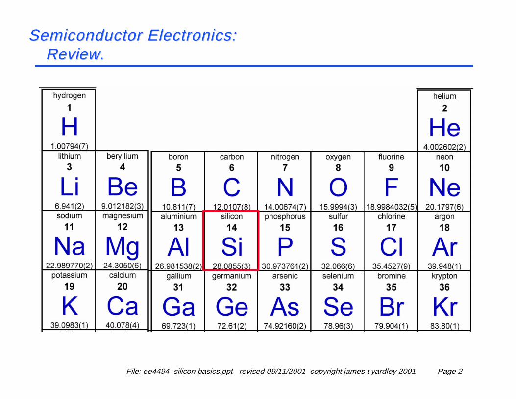
Semiconductor Electronics:Semiconductor Electronics:Review.Review.
File: ee4494 silicon basics.ppt revised 09/11/2001 copyright james t yardley 2001 Page 3
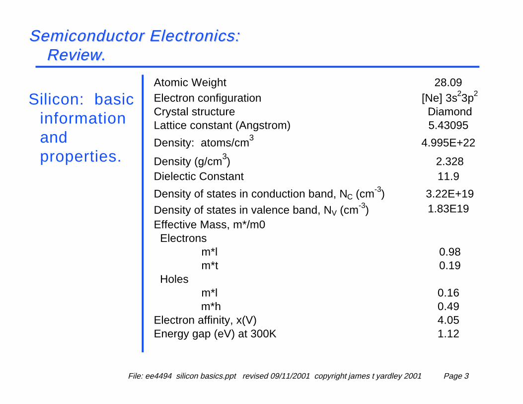
Semiconductor Electronics:Semiconductor Electronics:Review.Review.
Silicon: basic information and properties.
Atomic Weight 28.09 Electron configuration [Ne] 3s23p2
Crystal structure DiamondLattice constant (Angstrom) 5.43095
Density: atoms/cm3 4.995E+22
Density (g/cm3) 2.328Dielectic Constant 11.9
Density of states in conduction band, NC (cm-3) 3.22E+19Density of states in valence band, NV (cm-3) 1.83E19 Effective Mass, m*/m0 Electrons m*l 0.98 m*t 0.19 Holes m*l 0.16 m*h 0.49 Electron affinity, x(V) 4.05 Energy gap (eV) at 300K 1.12
File: ee4494 silicon basics.ppt revised 09/11/2001 copyright james t yardley 2001 Page 4
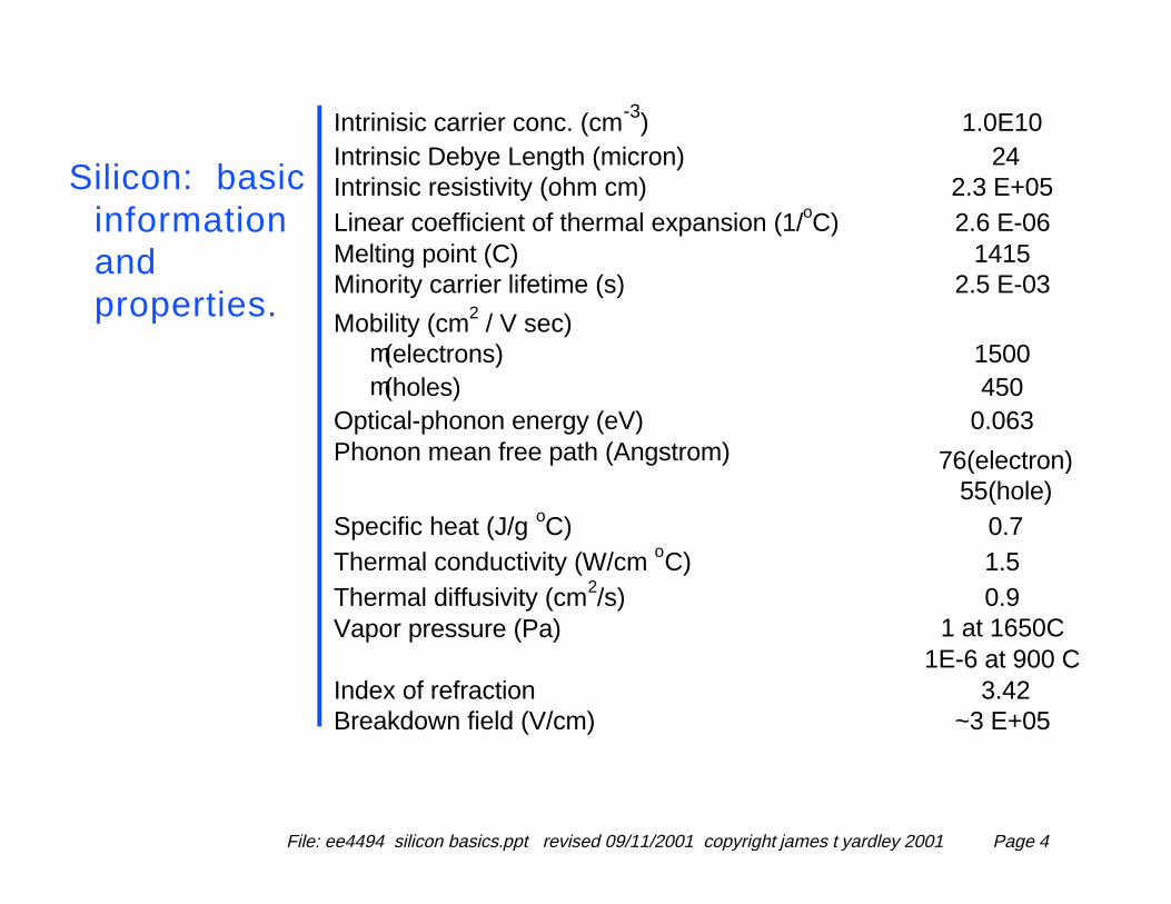
Silicon: basic information and properties.
Intrinisic carrier conc. (cm-3) 1.0E10 Intrinsic Debye Length (micron) 24Intrinsic resistivity (ohm cm) 2.3 E+05 Linear coefficient of thermal expansion (1/oC) 2.6 E-06 Melting point (C) 1415 Minority carrier lifetime (s) 2.5 E-03 Mobility (cm2 / V sec) µ(electrons) 1500 µ(holes) 450 Optical-phonon energy (eV) 0.063
76(electron)55(hole)
Specific heat (J/g oC) 0.7Thermal conductivity (W/cm oC) 1.5 Thermal diffusivity (cm2/s) 0.9
1 at 1650C 1E-6 at 900 C
Index of refraction 3.42Breakdown field (V/cm) ~3 E+05
Phonon mean free path (Angstrom)
Vapor pressure (Pa)

File: ee4494 silicon basics.ppt revised 09/11/2001 copyright james t yardley 2001 Page 5
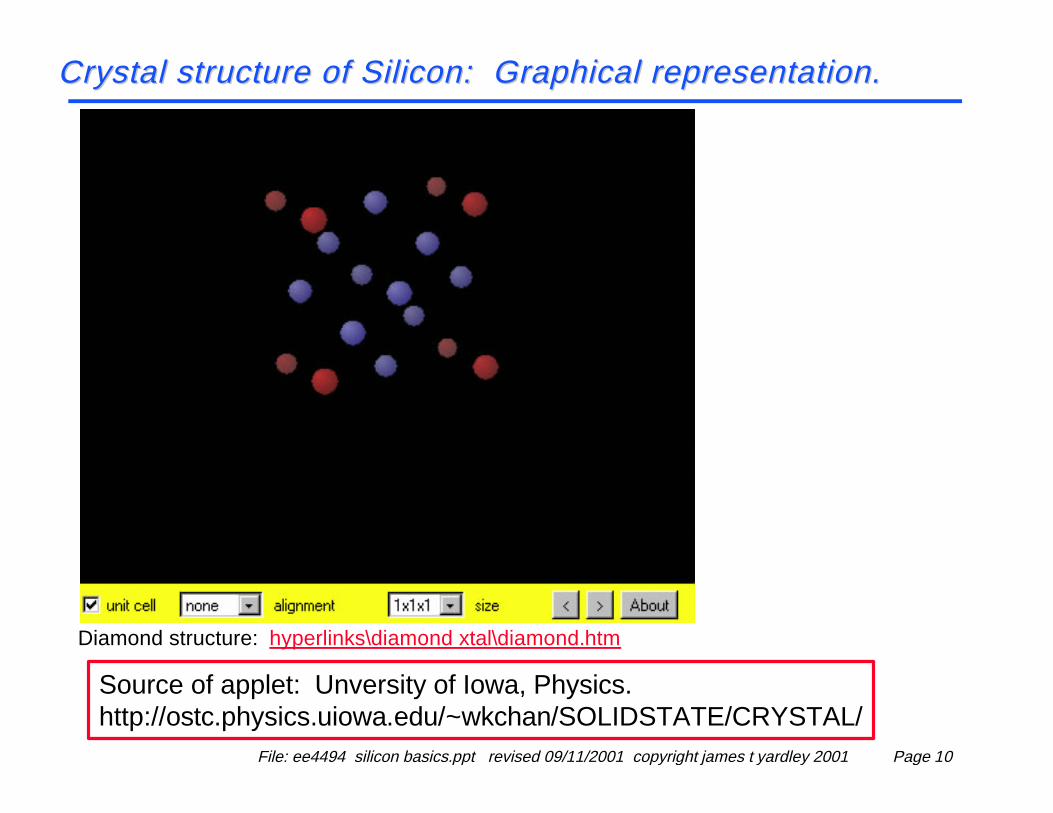
Crystal structure of silicon (diamond structure).Crystal structure of silicon (diamond structure).
hyperlinks\silicon\@silicon java\cell.html
Source of applet is Semiconductor Applet Service, SUNY, Buffalo:http://jas2.eng.buffalo.edu/applets/education/solid/unitCell/home.html
File: ee4494 silicon basics.ppt revised 09/11/2001 copyright james t yardley 2001 Page 6
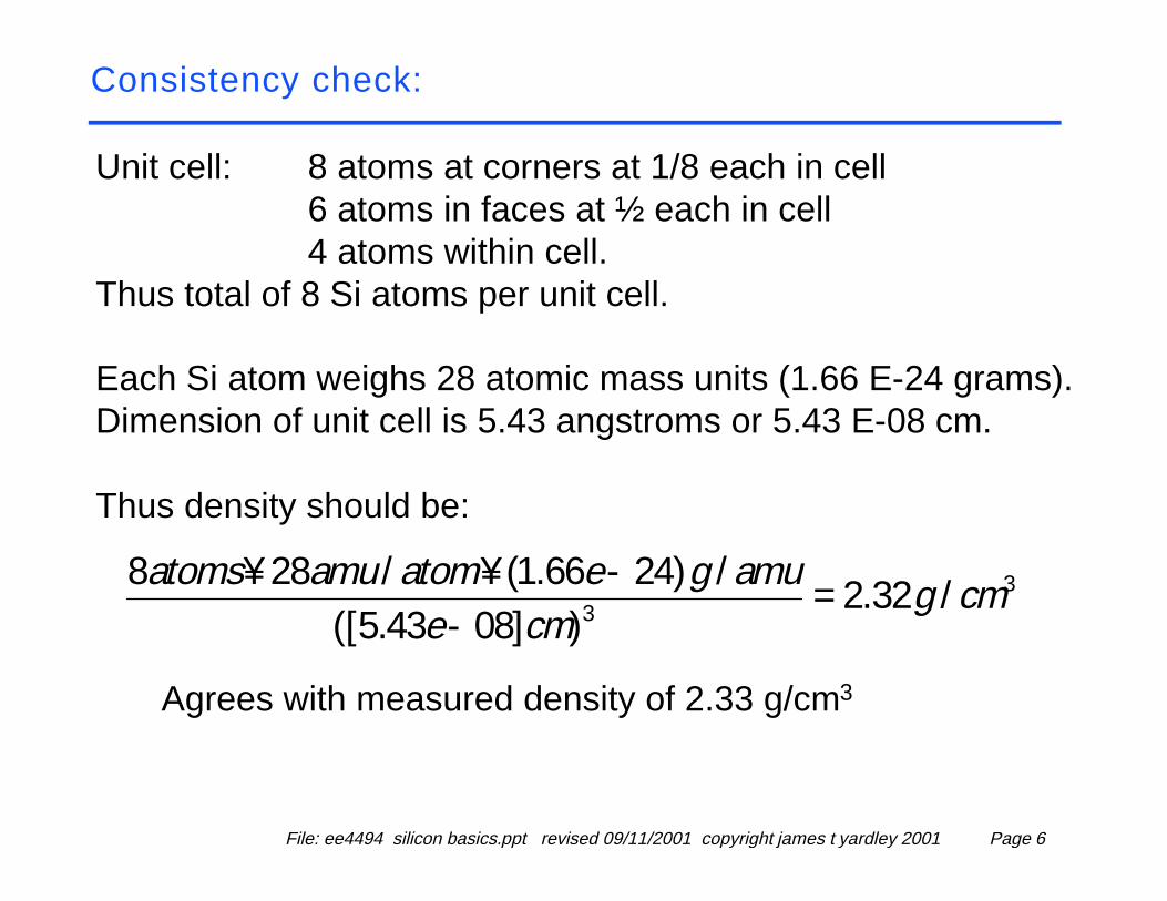
Unit cell: 8 atoms at corners at 1/8 each in cell6 atoms in faces at ½ each in cell4 atoms within cell.
Thus total of 8 Si atoms per unit cell.
Each Si atom weighs 28 atomic mass units (1.66 E-24 grams).Dimension of unit cell is 5.43 angstroms or 5.43 E-08 cm.
Thus density should be:
33 /32.2
)]0843.5([/)2466.1(/288 cmg
cmeamugeatomamuatoms =
−−××
Agrees with measured density of 2.33 g/cm3
Consistency check:

File: ee4494 silicon basics.ppt revised 09/11/2001 copyright james t yardley 2001 Page 7
Crystal planes of Silicon and Miller Indexes.Crystal planes of Silicon and Miller Indexes.
Start with unit cell with unit dimension along all axes.Plane can be defined in terms of intercepts along 3 unit cell axes.
1=++γβαzyx
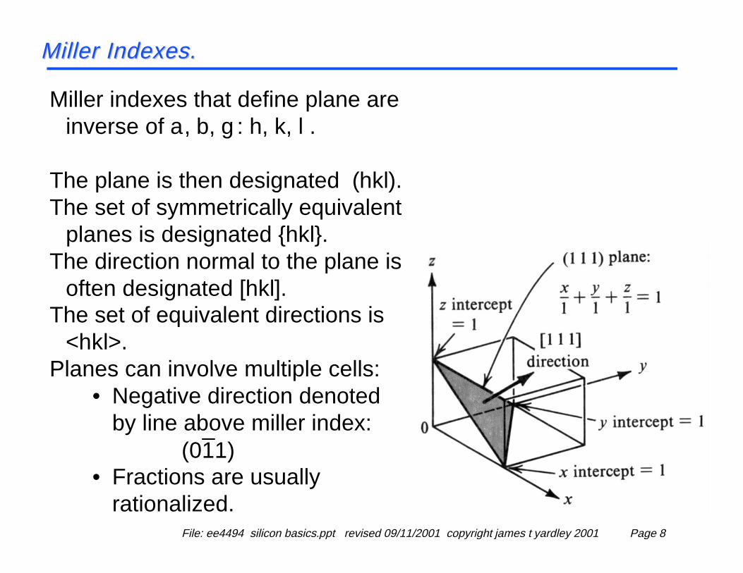
File: ee4494 silicon basics.ppt revised 09/11/2001 copyright james t yardley 2001 Page 8
Miller indexes that define plane are inverse of α, β, γ : h, k, l .
The plane is then designated (hkl).The set of symmetrically equivalent
planes is designated {hkl}.The direction normal to the plane is
often designated [hkl].The set of equivalent directions is
<hkl>.Planes can involve multiple cells:
• Negative direction denoted by line above miller index:
• Fractions are usually rationalized.
Miller Indexes.Miller Indexes.
(011)_

File: ee4494 silicon basics.ppt revised 09/11/2001 copyright james t yardley 2001 Page 9
(111) Plane
_(110) Plane
Set of (120) planes
Miller indexes for silicon: examples.Miller indexes for silicon: examples.
File: ee4494 silicon basics.ppt revised 09/11/2001 copyright james t yardley 2001 Page 10
Diamond structure: hyperlinks\diamond xtal\diamond.htm
Crystal structure of Silicon: Graphical representation.Crystal structure of Silicon: Graphical representation.
Source of applet: Unversity of Iowa, Physics.http://ostc.physics.uiowa.edu/~wkchan/SOLIDSTATE/CRYSTAL/

File: ee4494 silicon basics.ppt revised 09/11/2001 copyright james t yardley 2001 Page 11
http://www.fhi-berlin.mpg.de/grz/pub/surfexp/SXinput.html
Crystal geometries … continued.Crystal geometries … continued.
File: ee4494 silicon basics.ppt revised 09/11/2001 copyright james t yardley 2001 Page 12
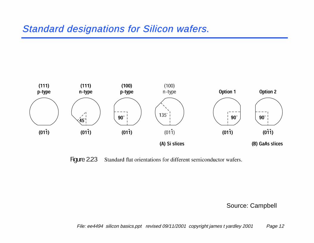
Standard designations for Silicon wafers.Standard designations for Silicon wafers.
Source: Campbell
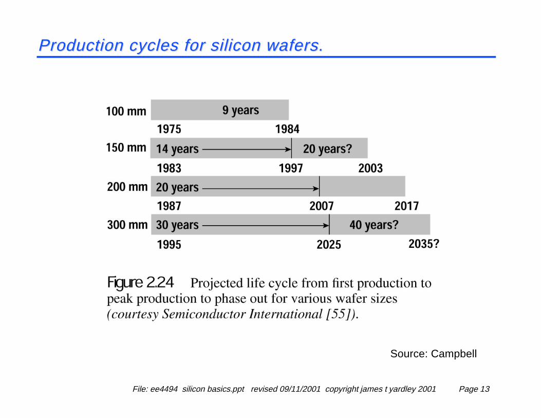
File: ee4494 silicon basics.ppt revised 09/11/2001 copyright james t yardley 2001 Page 13
Source: Campbell
Production cycles for silicon wafers.Production cycles for silicon wafers.
File: ee4494 silicon basics.ppt revised 09/11/2001 copyright james t yardley 2001 Page 14
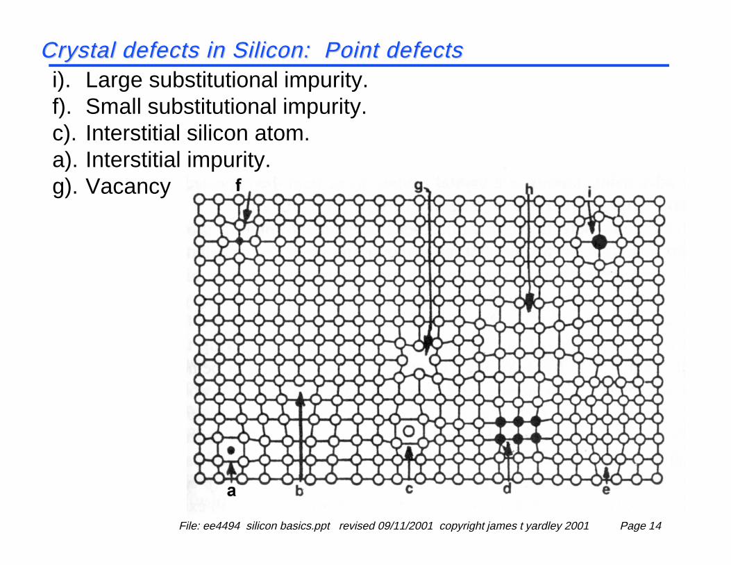
Crystal defects in Silicon: Point defectsCrystal defects in Silicon: Point defectsi). Large substitutional impurity.f). Small substitutional impurity.c). Interstitial silicon atom.a). Interstitial impurity.g). Vacancy

File: ee4494 silicon basics.ppt revised 09/11/2001 copyright james t yardley 2001 Page 15
Crystal Defects: Line defectsCrystal Defects: Line defectsExample: edge dislocation
Crystal Defects: Area defectsCrystal Defects: Area defects
Crystal Defects: Volume defectsCrystal Defects: Volume defects
Grain boundaries.Surfaces.….more…
Precipitates.Voids.….more…
File: ee4494 silicon basics.ppt revised 09/11/2001 copyright james t yardley 2001 Page 16
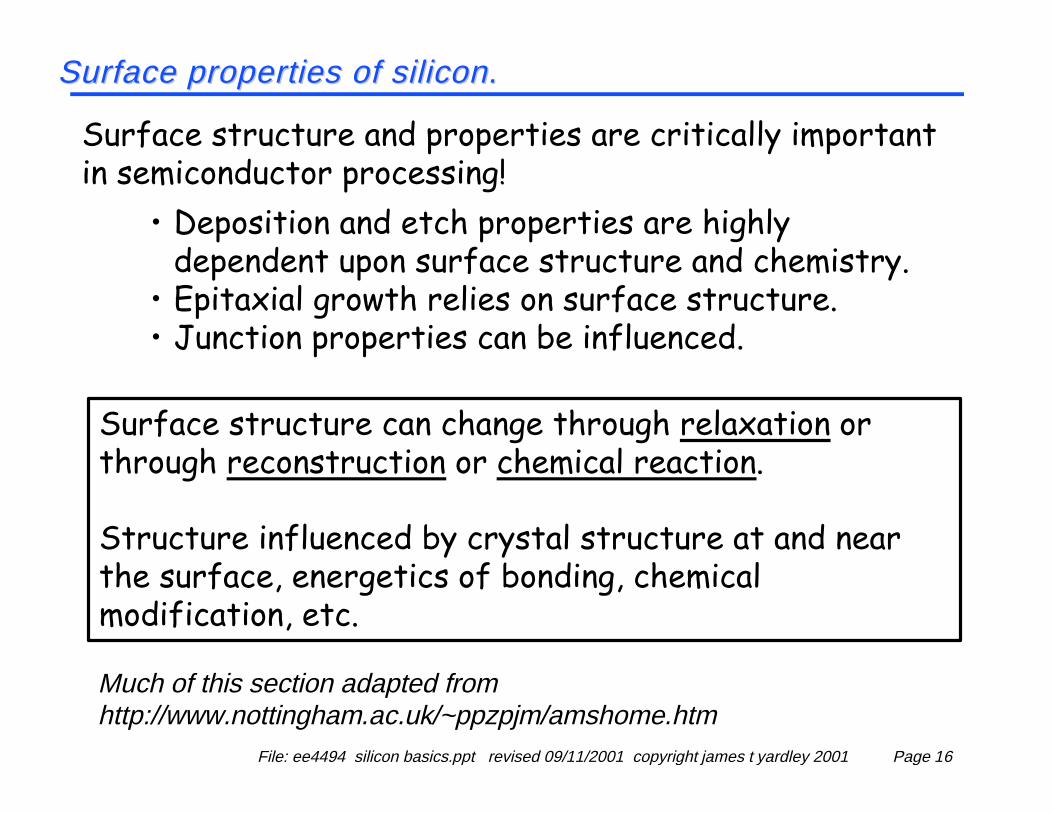
Surface properties of silicon.Surface properties of silicon.
Surface structure and properties are critically important in semiconductor processing!
• Deposition and etch properties are highly dependent upon surface structure and chemistry.
• Epitaxial growth relies on surface structure.• Junction properties can be influenced.
Much of this section adapted from http://www.nottingham.ac.uk/~ppzpjm/amshome.htm
Surface structure can change through relaxation or through reconstruction or chemical reaction.
Structure influenced by crystal structure at and near the surface, energetics of bonding, chemical modification, etc.
File: ee4494 silicon basics.ppt revised 09/11/2001 copyright james t yardley 2001 Page 17
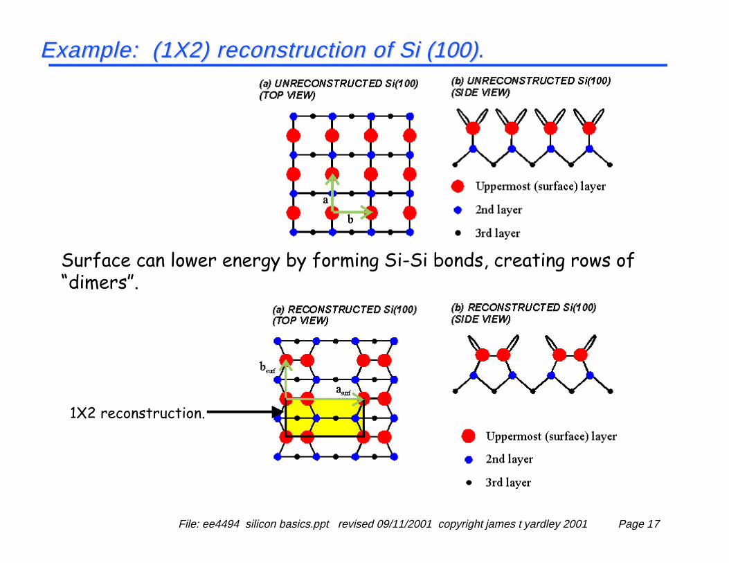
Example: (1X2) reconstruction of Example: (1X2) reconstruction of Si Si (100).(100).
Surface can lower energy by forming Si-Si bonds, creating rows of “dimers”.
1X2 reconstruction.

File: ee4494 silicon basics.ppt revised 09/11/2001 copyright james t yardley 2001 Page 18
Example: (1X2) reconstruction of Example: (1X2) reconstruction of Si Si (100)…continued.(100)…continued.
After reconstruction:“Cleaved” (100) surface:
Scanning Tunneling Microscope (STM) images of Si(100) after reconstruction showing rows of dimers on surface.

File: ee4494 silicon basics.ppt revised 09/11/2001 copyright james t yardley 2001 Page 19
Complex example: (7X7) reconstruction of Complex example: (7X7) reconstruction of Si Si (111).(111).
Note: elucidation of this structure has been subject of over 30 years of research.
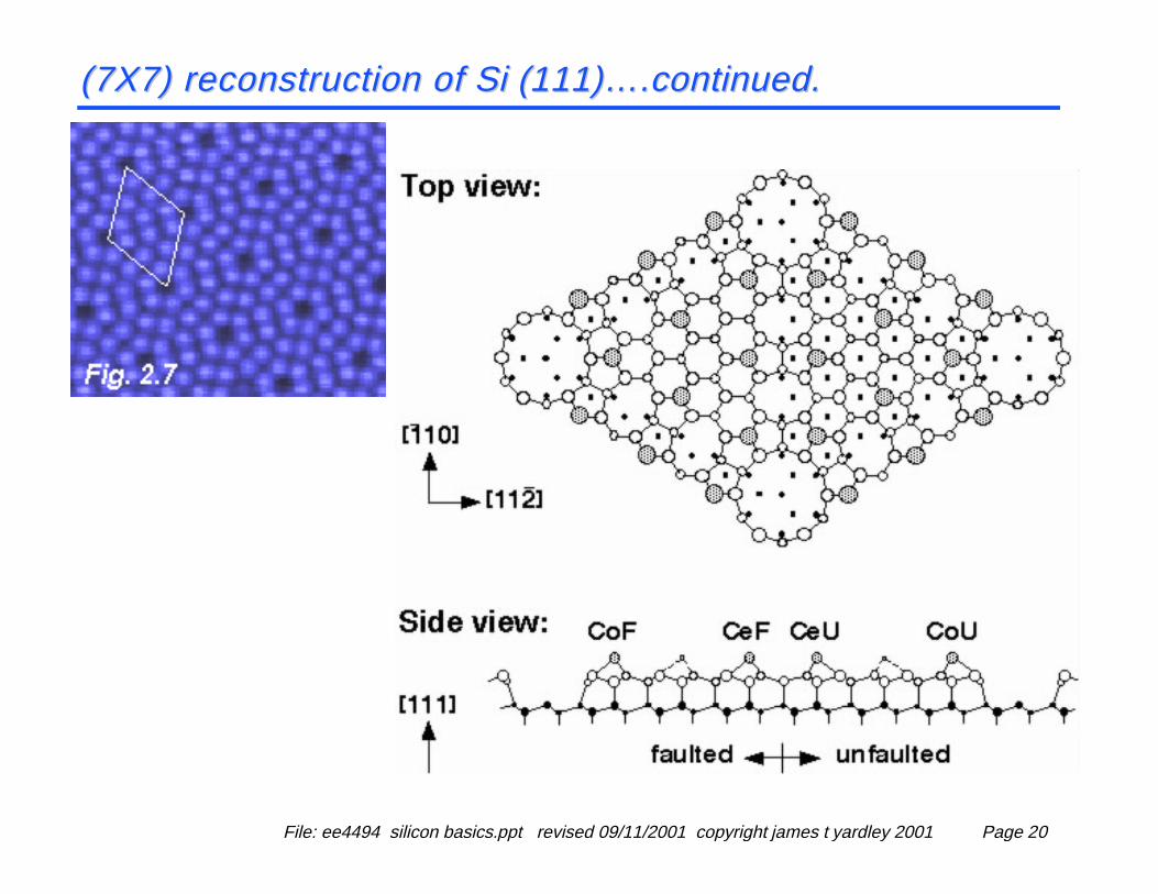
File: ee4494 silicon basics.ppt revised 09/11/2001 copyright james t yardley 2001 Page 20
(7X7) reconstruction of (7X7) reconstruction of Si Si (111)….continued.(111)….continued.
File: ee4494 silicon basics.ppt revised 09/11/2001 copyright james t yardley 2001 Page 21
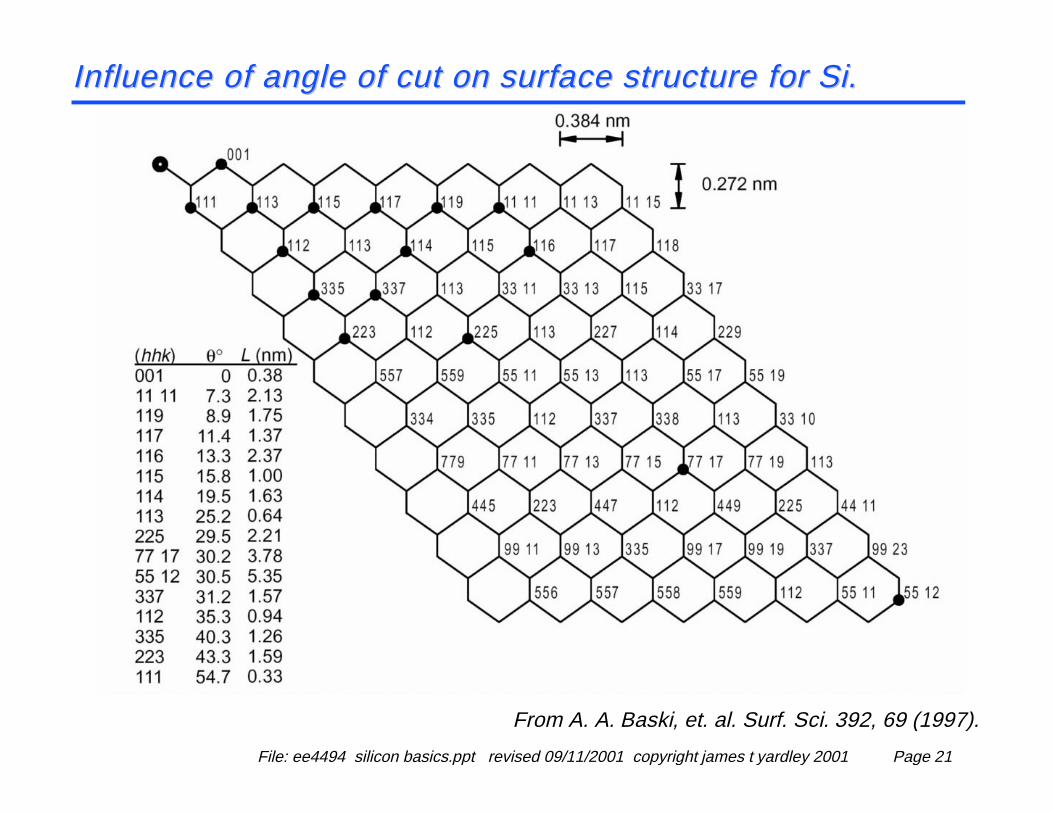
Influence of angle of cut on surface structure for Influence of angle of cut on surface structure for SiSi..
From A. A. Baski, et. al. Surf. Sci. 392, 69 (1997).
File: ee4494 silicon basics.ppt revised 09/11/2001 copyright james t yardley 2001 Page 22
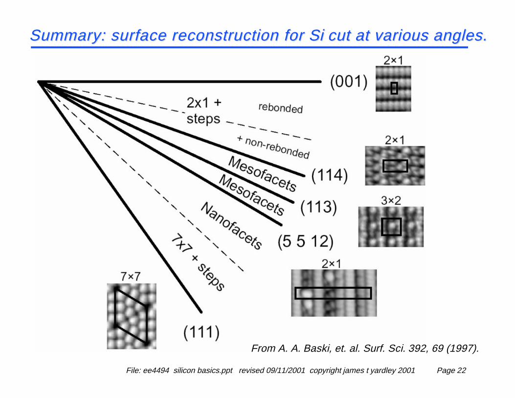
Summary: surface reconstruction for Summary: surface reconstruction for SiSi cut at various angles.cut at various angles.
From A. A. Baski, et. al. Surf. Sci. 392, 69 (1997).

File: ee4494 silicon basics.ppt revised 09/11/2001 copyright james t yardley 2001 Page 23
Steps and defects in surface structure.Steps and defects in surface structure.
“dangling bonds”

File: ee4494 silicon basics.ppt revised 09/11/2001 copyright james t yardley 2001 Page 24
Steps and defects in surface structure.Steps and defects in surface structure.
150 nm ~15 nm
STM of Si(100) showing 6 atomic steps.
Expanded STM of Si(100) showing dimer structure of adjacent atomic steps and other defects.STM is scanning tunneling microscope.

File: ee4494 silicon basics.ppt revised 09/11/2001 copyright james t yardley 2001 Page 25
Influence of chemical modification on surface structure.Influence of chemical modification on surface structure.
From A. Laracuente and L. J. Whitman, Surf. Sci. 476,L247 (2001).

File: ee4494 silicon basics.ppt revised 09/11/2001 copyright james t yardley 2001 Page 26
Electronic Properties of Silicon Electronic Properties of Silicon and Related Materialsand Related Materials

File: ee4494 silicon basics.ppt revised 09/11/2001 copyright james t yardley 2001 Page 27
Electronic properties of materials Electronic properties of materials –– general case.general case.
Insulators.Conductors.
Semi-conductors.
File: ee4494 silicon basics.ppt revised 09/11/2001 copyright james t yardley 2001 Page 28
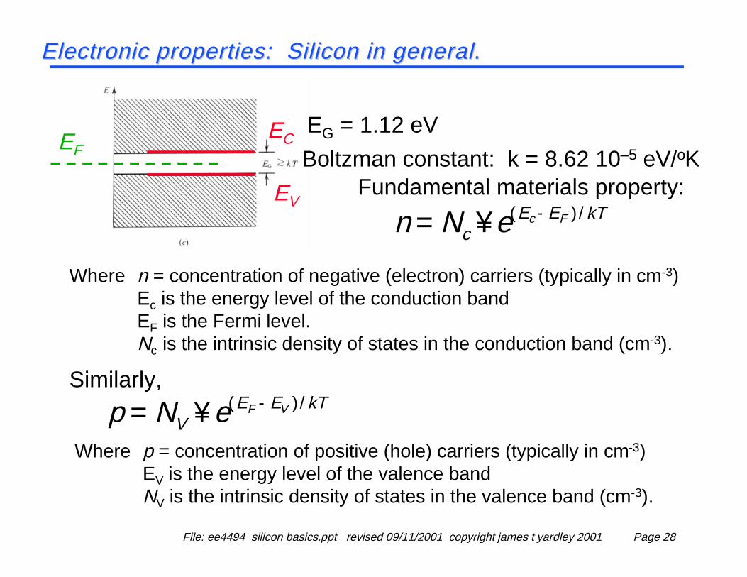
Electronic properties: Silicon in general. Electronic properties: Silicon in general.
EG = 1.12 eVBoltzman constant: k = 8.62 10–5 eV/oK
kTEEc
FceNn /)( −×=Fundamental materials property:
Where n = concentration of negative (electron) carriers (typically in cm-3)Ec is the energy level of the conduction bandEF is the Fermi level.Nc is the intrinsic density of states in the conduction band (cm-3).
EF
Similarly, kTEE
VVFeNp /)( −×=
Where p = concentration of positive (hole) carriers (typically in cm-3)EV is the energy level of the valence bandNV is the intrinsic density of states in the valence band (cm-3).
EC
EV
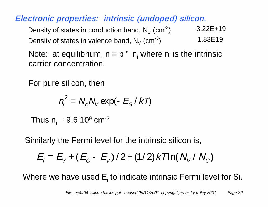
File: ee4494 silicon basics.ppt revised 09/11/2001 copyright james t yardley 2001 Page 29
Density of states in conduction band, NC (cm-3) 3.22E+19
Density of states in valence band, NV (cm-3) 1.83E19
Note: at equilibrium, n = p ≡ ni where ni is the intrinsic carrier concentration.
For pure silicon, then
)/exp(2 kTENNn GVci −=
Thus ni = 9.6 109 cm-3
Similarly the Fermi level for the intrinsic silicon is,
)/ln()2/1(2/)( CVVCVi NNkTEEEE +−+=
Where we have used Ei to indicate intrinsic Fermi level for Si.
Electronic properties: intrinsic (Electronic properties: intrinsic (undopedundoped) silicon. ) silicon.
File: ee4494 silicon basics.ppt revised 09/11/2001 copyright james t yardley 2001 Page 30
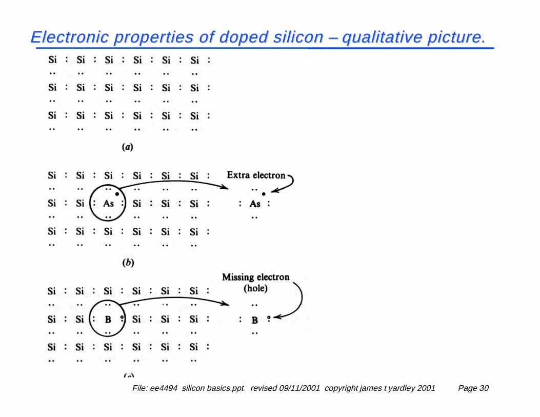
Electronic properties of doped silicon Electronic properties of doped silicon –– qualitative picture.qualitative picture.
File: ee4494 silicon basics.ppt revised 09/11/2001 copyright james t yardley 2001 Page 31
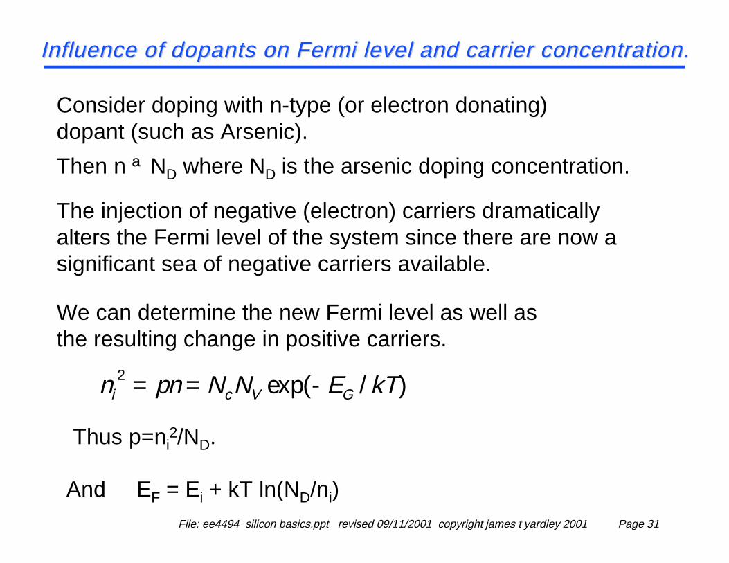
Consider doping with n-type (or electron donating) dopant (such as Arsenic).Then n ≈ ND where ND is the arsenic doping concentration.
The injection of negative (electron) carriers dramatically alters the Fermi level of the system since there are now a significant sea of negative carriers available.
We can determine the new Fermi level as well as the resulting change in positive carriers.
)/exp(2 kTENNpnn GVci −==
Thus p=ni2/ND.
And EF = Ei + kT ln(ND/ni)
Influence of Influence of dopants dopants on Fermi level and carrier concentration.on Fermi level and carrier concentration.

File: ee4494 silicon basics.ppt revised 09/11/2001 copyright james t yardley 2001 Page 32
Correspondingly, for p-type (acceptor) dopants such at B:
Thus n=ni2/NA.
And EF = Ei - kT ln(NA/ni)
Resistivity
)(1
pn pnq µµρ
+=
Where q is electron chargeand µ are mobilities.
Influence of Influence of dopants dopants on resistance.on resistance.
File: ee4494 silicon basics.ppt revised 09/11/2001 copyright james t yardley 2001 Page 33
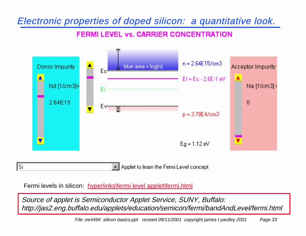
Fermi levels in silicon: hyperlinks\fermi level applet\fermi.html
Source of applet is Semiconductor Applet Service, SUNY, Buffalo:http://jas2.eng.buffalo.edu/applets/education/semicon/fermi/bandAndLevel/fermi.html
Electronic properties of doped silicon: a quantitative look. Electronic properties of doped silicon: a quantitative look.

File: ee4494 silicon basics.ppt revised 09/11/2001 copyright james t yardley 2001 Page 34
The The pn pn junction: a qualitative view.junction: a qualitative view.

File: ee4494 silicon basics.ppt revised 09/11/2001 copyright james t yardley 2001 Page 35
The The pnpn junction: a more quantitative view.junction: a more quantitative view.
Link to pn junction: hyperlinks\pn junction\pnformation2.htm
Source of applet is Semiconductor Applet Service, SUNY, Buffalo:http://jas2.eng.buffalo.edu/applets/education/pn/pnformation2/pnformation2.html
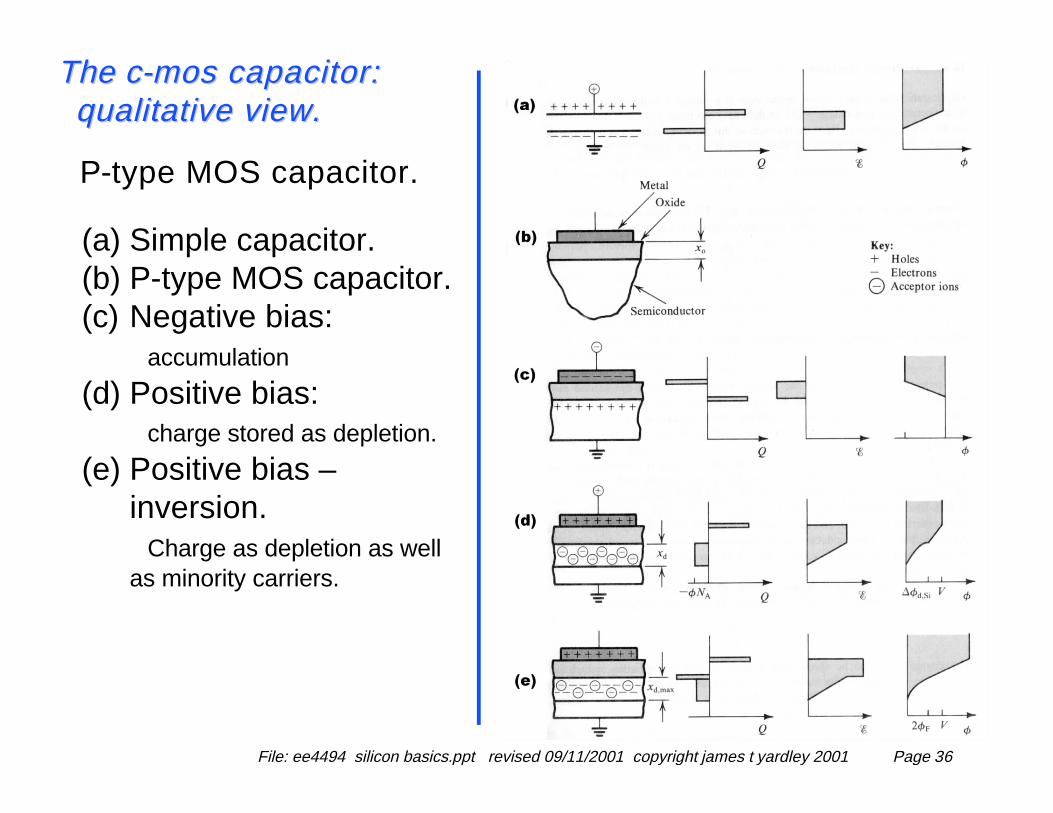
File: ee4494 silicon basics.ppt revised 09/11/2001 copyright james t yardley 2001 Page 36
The cThe c--mos mos capacitor:capacitor:qualitative view.qualitative view.
P-type MOS capacitor.
(a) Simple capacitor.(b) P-type MOS capacitor.(c) Negative bias:
accumulation
(d) Positive bias:charge stored as depletion.
(e) Positive bias –inversion.
Charge as depletion as well as minority carriers.

File: ee4494 silicon basics.ppt revised 09/11/2001 copyright james t yardley 2001 Page 37
The cThe c--mos mos capacitor: slightly more quantitative view.capacitor: slightly more quantitative view.
Link: hyperlinks\mos2\biasPot10.htm

File: ee4494 silicon basics.ppt revised 09/11/2001 copyright james t yardley 2001 Page 38
MOS devices and how they work…simple picture.MOS devices and how they work…simple picture.
NMOS transistor
P-type substrateN-type channel
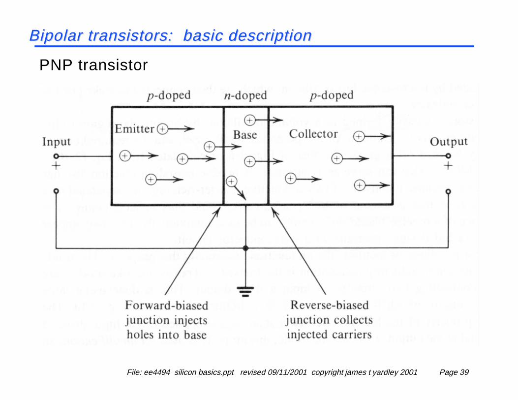
File: ee4494 silicon basics.ppt revised 09/11/2001 copyright james t yardley 2001 Page 39
Bipolar transistors: basic descriptionBipolar transistors: basic description
PNP transistor
Related Documents