Vol.:(0123456789) 1 3 Journal of Materials Science: Materials in Electronics (2020) 31:9719–9725 https://doi.org/10.1007/s10854-020-03517-1 Electrical properties of Graphene/Silicon structure with Al 2 O 3 interlayer Nuriye Kaymak 1 · Ozkan Bayram 2 · Adem Tataroğlu 3 · Sema Bilge Ocak 1 · Elif Oz Orhan 1,3 Received: 30 January 2020 / Accepted: 28 April 2020 / Published online: 12 May 2020 © Springer Science+Business Media, LLC, part of Springer Nature 2020 Abstract The electrical properties of the fabricated Al/Gr/Al 2 O 3 /p-Si structure have been analyzed using frequency-dependent capaci- tance/conductance–voltage (C/G–V) measurements. Graphene (Gr) nanosheets were grown on to copper (Cu) catalyst sub- strate, which has 99.99% purity, by Chemical Vapor Deposition (CVD) technique, and then the Graphene was transferred on Al 2 O 3 /p-Si by the standard transfer process. The Graphene structures have been characterized by Raman Spectroscopy and Transmission Electron Microscopy (TEM) analyses, and the results of both analyses confirmed the monolayer/bilayer Gra- phene nanostructure. The forward and reverse bias G–V and C–V measurements of this structure have been performed in 10 kHz–400 kHz and at 300 K. The frequency dispersion in C and G can be evaluated for interface state density ( D it ) and series resistance ( R s ) values. The values of D it and R s are dependent on frequency and increase with decreasing frequency. The R s - V graph shows a peak form at all frequencies in the depletion region and vanishes with increasing frequency. The obtained results suggest that the prepared structure can be used in electronic device applications. 1 Introduction Graphene (Gr) has attracted the attention of many research- ers, thanks to its excellent electrical [1–6], mechanical [7], optical [8], and thermal properties [9]. Graphene is one of the most significant among all two-dimensional (2D) mate- rials due to its important properties such as high thermal conductivity, high transparency, high electrical conductivity, high carrier mobility, low contact resistance, and mechani- cal flexibility [10]. Graphene is an impressive material for future electronics due to these properties and is used in various electronic and photonic devices such as transistors, electrodes, gas sensors, photodetectors, solar cells, micro- wave mixers, rectifiers, graphene variable-barrier “barris- tor”, and some integrated circuits [2–4]. These graphene- based devices combine the advantages of graphene with semiconductor technology. For example, the graphene/sili- con (Gr/Si) junction is one of the simplest devices. In the literature, various methods such as CVD, pulsed laser deposition (PLD), plasma-enhanced chemical vapor deposition (PECVD), and epitaxial growth have been used to grow Graphene and Graphene-based nanostructures. There is no standard method for the fabrication of the Gr/ Si structure. Each method involves different parameters in itself. Especially some parameters such as growth of Gra- phene, transfer process of Graphene, the effects of substrate and oxide layer, the geometry of the substrate, the effect of metal-Graphene contact should be reviewed together. Despite the excitement of both experimental and theoretical studies, the physics underlying the Graphene-semiconductor structure is unfinished yet [2, 4]. Up to now, some researchers examined Graphene-based Schottky structures [2–4, 11]. The source of the non-ideal Graphene-Silicon Schottky junction was examined by Zhang et al. [12]. They found that native oxide (SiO 2 ) is proved to be an important role in finding the behavior of a Gr-Si junction. Tomer et al. [13] fabricated Schottky junctions by CVD monolayer Gr on n-Si and GaAs wafers and investigated inhomogeneity in barrier height Gr/Si (or GaAs) structures. Luongo et al. [14] studied the impor- tance of the wafer in Gr/Si photodiodes. They concluded that the substrate tip geometry effects Gr/p-Si Schottky * Elif Oz Orhan [email protected] 1 Advanced Technologies, Gazi University, 06500 Ankara, Turkey 2 Central Application and Research Laboratory (BUMER), Bayburt University, 69100 Bayburt, Turkey 3 Physics, Gazi University, 06500 Ankara, Turkey

Welcome message from author
This document is posted to help you gain knowledge. Please leave a comment to let me know what you think about it! Share it to your friends and learn new things together.
Transcript
Vol.:(0123456789)1 3
Journal of Materials Science: Materials in Electronics (2020) 31:9719–9725 https://doi.org/10.1007/s10854-020-03517-1
Electrical properties of Graphene/Silicon structure with Al2O3 interlayer
Nuriye Kaymak1 · Ozkan Bayram2 · Adem Tataroğlu3 · Sema Bilge Ocak1 · Elif Oz Orhan1,3
Received: 30 January 2020 / Accepted: 28 April 2020 / Published online: 12 May 2020 © Springer Science+Business Media, LLC, part of Springer Nature 2020
AbstractThe electrical properties of the fabricated Al/Gr/Al2O3/p-Si structure have been analyzed using frequency-dependent capaci-tance/conductance–voltage (C/G–V) measurements. Graphene (Gr) nanosheets were grown on to copper (Cu) catalyst sub-strate, which has 99.99% purity, by Chemical Vapor Deposition (CVD) technique, and then the Graphene was transferred on Al2O3/p-Si by the standard transfer process. The Graphene structures have been characterized by Raman Spectroscopy and Transmission Electron Microscopy (TEM) analyses, and the results of both analyses confirmed the monolayer/bilayer Gra-phene nanostructure. The forward and reverse bias G–V and C–V measurements of this structure have been performed in 10 kHz–400 kHz and at 300 K. The frequency dispersion in C and G can be evaluated for interface state density ( D
it ) and
series resistance ( Rs ) values. The values of D
it and R
s are dependent on frequency and increase with decreasing frequency.
The Rs− V graph shows a peak form at all frequencies in the depletion region and vanishes with increasing frequency. The
obtained results suggest that the prepared structure can be used in electronic device applications.
1 Introduction
Graphene (Gr) has attracted the attention of many research-ers, thanks to its excellent electrical [1–6], mechanical [7], optical [8], and thermal properties [9]. Graphene is one of the most significant among all two-dimensional (2D) mate-rials due to its important properties such as high thermal conductivity, high transparency, high electrical conductivity, high carrier mobility, low contact resistance, and mechani-cal flexibility [10]. Graphene is an impressive material for future electronics due to these properties and is used in various electronic and photonic devices such as transistors, electrodes, gas sensors, photodetectors, solar cells, micro-wave mixers, rectifiers, graphene variable-barrier “barris-tor”, and some integrated circuits [2–4]. These graphene-based devices combine the advantages of graphene with
semiconductor technology. For example, the graphene/sili-con (Gr/Si) junction is one of the simplest devices.
In the literature, various methods such as CVD, pulsed laser deposition (PLD), plasma-enhanced chemical vapor deposition (PECVD), and epitaxial growth have been used to grow Graphene and Graphene-based nanostructures. There is no standard method for the fabrication of the Gr/Si structure. Each method involves different parameters in itself. Especially some parameters such as growth of Gra-phene, transfer process of Graphene, the effects of substrate and oxide layer, the geometry of the substrate, the effect of metal-Graphene contact should be reviewed together. Despite the excitement of both experimental and theoretical studies, the physics underlying the Graphene-semiconductor structure is unfinished yet [2, 4].
Up to now, some researchers examined Graphene-based Schottky structures [2–4, 11]. The source of the non-ideal Graphene-Silicon Schottky junction was examined by Zhang et al. [12]. They found that native oxide (SiO2) is proved to be an important role in finding the behavior of a Gr-Si junction. Tomer et al. [13] fabricated Schottky junctions by CVD monolayer Gr on n-Si and GaAs wafers and investigated inhomogeneity in barrier height Gr/Si (or GaAs) structures. Luongo et al. [14] studied the impor-tance of the wafer in Gr/Si photodiodes. They concluded that the substrate tip geometry effects Gr/p-Si Schottky
* Elif Oz Orhan [email protected]
1 Advanced Technologies, Gazi University, 06500 Ankara, Turkey
2 Central Application and Research Laboratory (BUMER), Bayburt University, 69100 Bayburt, Turkey
3 Physics, Gazi University, 06500 Ankara, Turkey
9720 Journal of Materials Science: Materials in Electronics (2020) 31:9719–9725
1 3
diode performance. The influence of temperature and light on the I–V/C–V properties of Gr/n-Si. Schottky diodes were characterized by Luongo et al. [15]. They notified a very high photocurrent and concluded that the structure enhances the photo-response of Gr/Si junction.
Herein we experimentally investigate the effect of inserting a high dielectric layer as (Aluminium oxide-Al2O3) between the Gr and Si. The layer acts as an electron blocking layer and the affective modulation of the Gra-phene’s Fermi level to passivate the silicon surface, which not only minimizes recombination but also increases the built-in potential. Therefore, Al2O3 was used as a high dielectric layer between the Gr and Si. The benefits of Al2O3 interfacial layers are not only limited to reducing the recombination at the interface but it also creates a higher Schottky barrier. Al2O3 has been proven as a good passivation layer for Si substrate [16, 17]. Passivating the surface with Al2O3 prevents thick native oxide for-mation at the interface. Also, it creates a conformal and uniform Al2O3 layer passivating the Si surface effectively. Thus, the Al2O3 layer contributed to improving the carrier lifetime for Si substrate decreasing the series resistance, reducing the surface recombination, and decreasing the density of traps significantly causing a major reduction in the surface recombination. Consequently, the Al2O3 interlayer between Gr and Si plays an important role in improving C–V and G–V characteristics of the Al2O3 layer between the Gr and Si.
The interface state density ( Dit ) and series resistance (Rs) are important parameters affecting the electrical characteristics of semiconductor devices [18, 19]. The current–voltage (I–V), capacitance–voltage (C–V), and conductance method are used to determine the D
it and
Rs parameters. The Dit and Rs are strongly dependent on
alternating current frequency. Therefore, the C–V and G–V characteristics are sensitive to applied voltage and the fre-quency. The interface states cause the C–V curves to be stretched out along the gate voltage axis. The interface states cause the nonparallel shift or stretch out along the gate voltage axis of the C–V curves.
In this research article, we investigated the frequency-sensitive capacitance/conductance-voltage (C/G–V) charac-teristics of the Al/Gr/Al2O3/p-Si structure. The admittance measurements (Y = G + iωC) were performed in the fre-quency range of 10 kHz–400 kHz and at 300 K. The voltage limit was adjusted to ±5V dc. The electrical parameters such as interface states and series resistance of the structure were extracted from the admittance measurements. Aluminum oxide (Al2O3) thin films were deposited at room tempera-ture onto the p-Si wafer by Radio Frequency (RF) magnetron sputtering. The CVD method, which is the standard method [3] was applied for the deposition of monolayer graphene onto Al2O3/p-type Si.
2 Experimental details
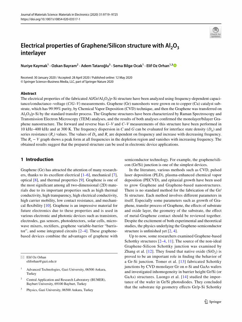
In this study, firstly, Graphene nanosheets were deposited on the copper (Cu) (99.99% purity from Alpha Easer) substrates by using the CVD procedure. The procedure is widely used to obtain homogenous and single-layer Graphene nanosheets compared to other techniques. CH4 gas as the carbon source, H2 gas for both the diluent gas and the annealing process gas, and Ar and H2 gases were used together to facilitate the breakdown CH4 precursor. First of all, the Cu substrates were cut to size 2 cm × 2 cm, and no surface cleaning was performed for these substrates. These Cu substrates were placed in the substrate compartment of the CVD technique and the pressure of the vacuum medium was set to 1 mTorr with the help of the vacuum pump. At this pressure, anneal-ing of these metal substrates was carried out. First, the tem-perature of the vacuum medium was removed from 24 °C to 1000 °C by 40 minutes using the heater. The process was executed by using 20 sccm H2 gas and 15 sccm Ar gas for 30 minutes at 1000 °C. The Gr thin films were then obtained by sending 7 sccm CH4 gas to the vacuum medium without changing the gas flow rates of these gases for 30 minutes. Growth details of Gr nanosheets are presented in Fig. 1 [15]. After the growth procedure, the Gr nanosheets were moved onto the above-mentioned (Al2O3)/p-Si structure. After the growth procedure, the Gr transfer process on to Al2O3/p-Si structure was occurred using with standard approach Poly(methyl methacrylate (PMMA)/Iron(III) Chlo-ride (FeCl3) as seen in Fig. 2 [16].
The numbers of CVD graphene layers were determined by using Raman analysis. Raman analysis provides detailed information to investigate the characteristic peaks of carbon-based films and to determine the number of layers by calcu-lating the ratios of these peaks relative to each other. How-ever, optical transmittance analysis and TEM analysis are also preferred for the detection of Graphene layer numbers
Fig. 1 Graphene growth mechanism on Cu foil by the CVD method
9721Journal of Materials Science: Materials in Electronics (2020) 31:9719–9725
1 3
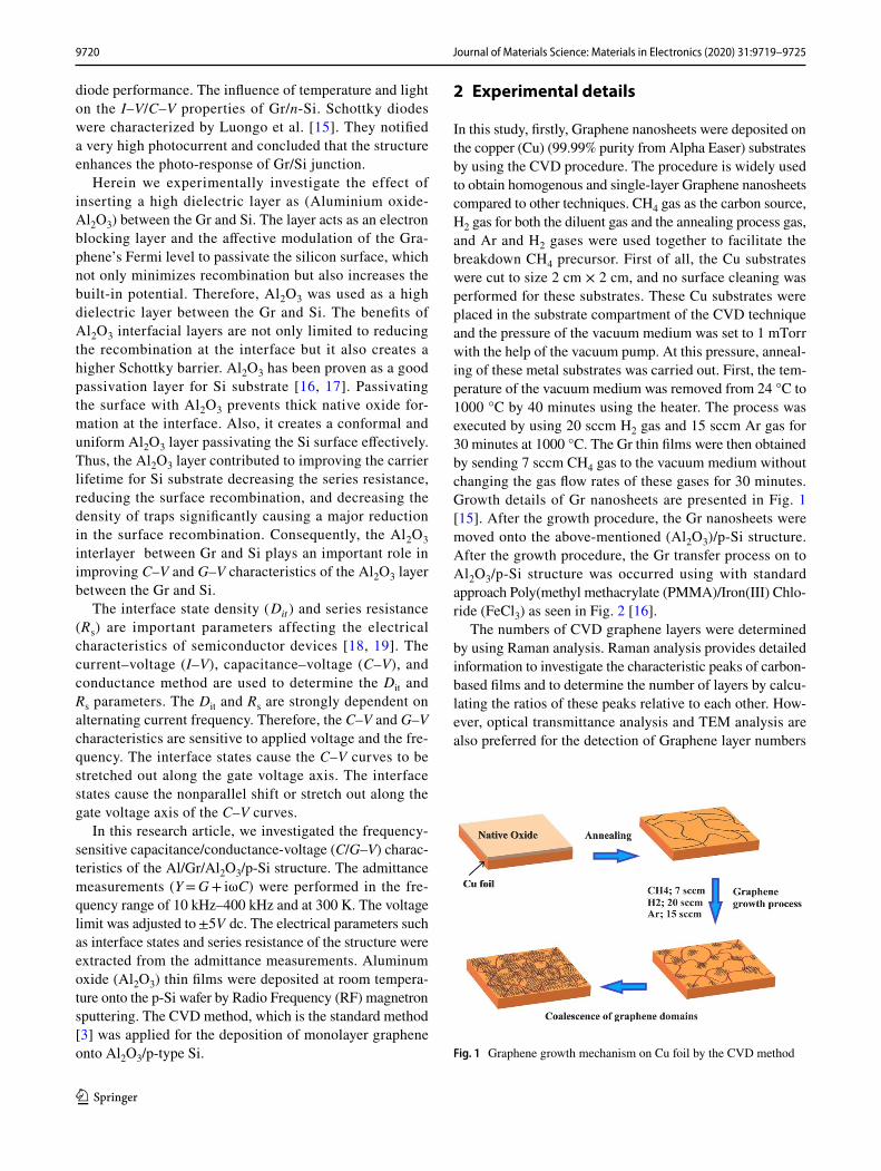
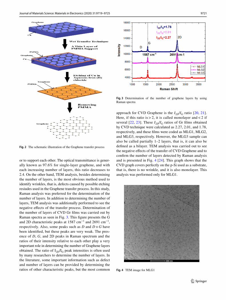
or to support each other. The optical transmittance is gener-ally known as 97.6% for single-layer graphene, and with each increasing number of layers, this ratio decreases to 2.4. On the other hand, TEM analysis, besides determining the number of layers, is the most obvious method used to identify wrinkles, that is, defects caused by possible etching resiudes used in the Graphene transfer process. In this study, Raman analysis was preferred for the determination of the number of layers. In addition to determining the number of layers, TEM analysis was additionally performed to see the negative effects of the transfer process. Determination of the number of layers of CVD Gr films was carried out by Raman spectra as seen in Fig. 3. This figure presents the G and 2D characteristic peaks at 1587 cm−1 and 2691 cm−1, respectively. Also, some peaks such as D and D + G have been identified, but these peaks are very weak. The pres-ence of D, G, and 2D peaks in Raman spectrum and the ratios of their intensity relative to each other play a very important role in determining the number of Graphene layers obtained. The ratio of I2D/IG peak intensities is often used by many researchers to determine the number of layers. In the literature, some important information such as defect and number of layers can be provided by determining the ratios of other characteristic peaks, but the most common
approach for CVD Graphene is the I2D/IG ratio [20, 21]. Here, if this ratio is > 2, it is called monolayer and < 2 if several [22, 23]. These I2D/IG ratios of Gr films obtained by CVD technique were calculated as 2.27, 2.01, and 1.78, respectively, and these films were coded as MLG1, MLG2, and MLG3, respectively. However, the MLG3 sample can also be called partially 1–2 layers, that is, it can also be defined as a bilayer. TEM analysis was carried out to see the negative effects of the transfer of CVD Graphene and to confirm the number of layers detected by Raman analysis and is presented in Fig. 4 [24]. This graph shows that the CVD graph covers perfectly on the p-Si used as a substrate, that is, there is no wrinkle, and it is also monolayer. This analysis was performed only for MLG1.
Fig. 2 The schematic illustration of the Graphene transfer process
Fig. 3 Determination of the number of graphene layers by using Raman spectra
Fig. 4 TEM image for MLG1
9722 Journal of Materials Science: Materials in Electronics (2020) 31:9719–9725
1 3
124 nm thick Aluminum (Al) (pureness: 99.99%) for an ohmic contact was coated by using the thermal evapora-tion (TE) technique. To dope Al into the unpolished sur-face of the p-type Si (100), the p-Si (having resistivity of 1–10 Ω cm, the diameter of 2 inches, and thickness of 280 µm) was annealed at 500 °C/10 min in vacuum by TE technique. Later, Al2O3 thin films were deposited at room temperature onto p-Si by RF magnetron sputtering. For this, an Al2O3 target of 99.9% purity was used. The power was 150 W and the base pressure inside the chamber was always 3.3 × 10⁻⁷ mbar. The coating pressure was 4.2.10–3 mbar. The target to substrate distance was fixed at 50 mm to achieve a better homogeneity. The working gas was 99.99% Ar. Ar/O2 gas flow ratio was 9/1 and Ar flow rate was12 sccm, O2 flow rate was 1.3 sccm. The deposition rate is 0.1 Å/s. The thickness of Al2O3 was 17 nm. The Al2O3/p-Si structure was immersed in deionized water so that the Gr thin film was placed on this structure. In the final step, the thickness of 128 nm Al metal for rectifying contacts was deposited using by TE technique on Gr nanosheet by a 1 mm diameter metal mask. Figure 5 shows the schematic profile of the pre-pared Al/Gr/Al2O3/p-Si structure.
3 Results and discussion
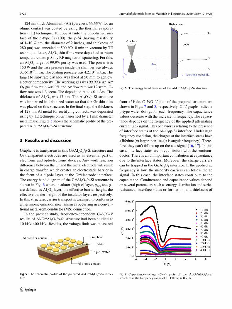
Graphene is transparent in this Gr/Al2O3/p-Si structure and Gr transparent electrodes are used as an essential part of electronic and optoelectronic devices. Any work function difference between the Gr and the metal electrode will result in charge transfer, which creates an electrostatic barrier in the form of a dipole layer at the Gr/electrode interface. The energy band diagram of the Gr/Al2O3/p-Si structure is shown in Fig. 6 where insulator (high-κ) layer, �
bm and �
T
are defined as Al2O3 layer, the effective barrier height, the effective barrier height of the insulator layer, respectively. In this structure, carrier transport is assumed to conform to a thermionic emission mechanism as occurring in a conven-tional metal-semiconductor (MS) connection.
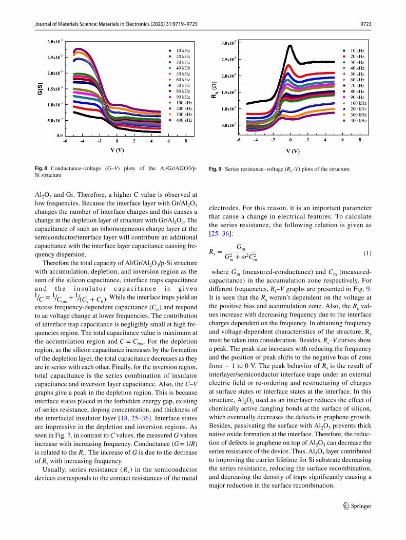
In the present study, frequency-dependent G–V/C–V results of Al/Gr/Al2O3/p-Si structure had been studied at 10 kHz-400 kHz. Besides, the voltage limit was measured
from ±5V dc. C–V/G–V plots of the prepared structure are shown in Figs. 7 and 8, respectively. C–V graphs indicate p-type wafer doings for each frequency. The capacitance values decrease with the increase in frequency. The capaci-tance depends on the frequency of the applied alternating current (ac) signal. This behavior is relating to the presence of interface states at the Al2O3/p-Si interface. Under high frequency condition, the charges at the interface states have a lifetime (τ) larger than 1/ω (ω is angular frequency). There-fore, they can’t follow up on the aac signal [16, 17]. In this case, interface states are in equilibrium with the semicon-ductor. There is an unimportant contribution at capacitance due to the interface states. Moreover, the charge carriers can be trapped in the Gr/Al2O3 interface. If the applied ac frequency is low, the minority carriers can follow the ac signal. In this case, the interface states contribute to the capacitance. Conductance and capacitance values depend on several parameters such as energy distribution and series resistance, interface states or formation, and thickness of
Fig. 5 The schematic profile of the prepared Al/Gr/Al2O3/p-Si struc-ture
Fig. 6 The energy band diagram of the Al/Gr/Al2O3/p-Si structure
Fig. 7 Capacitance–voltage (C–V) plots of the Al/Gr/Al2O3/p-Si structure in the frequency range of 10 kHz to 400 kHz
9723Journal of Materials Science: Materials in Electronics (2020) 31:9719–9725
1 3
Al2O3 and Gr. Therefore, a higher C value is observed at low frequencies. Because the interface layer with Gr/Al2O3 changes the number of interface charges and this causes a change in the depletion layer of structure with Gr/Al2O3. The capacitance of such an inhomogeneous charge layer at the semiconductor/interface layer will contribute an additional capacitance with the interface layer capacitance causing fre-quency dispersion.
Therefore the total capacity of Al/Gr/Al2O3/p-Si structure with accumulation, depletion, and inversion region as the sum of the silicon capacitance, interface traps capacitance a n d t h e i n s u l a t o r c a p a c i t a n c e i s g i ve n 1∕C =
1∕C
ins+1∕(C
s+ C
it) . While the interface traps yield an
excess frequency-dependent capacitance ( Cit ) and respond
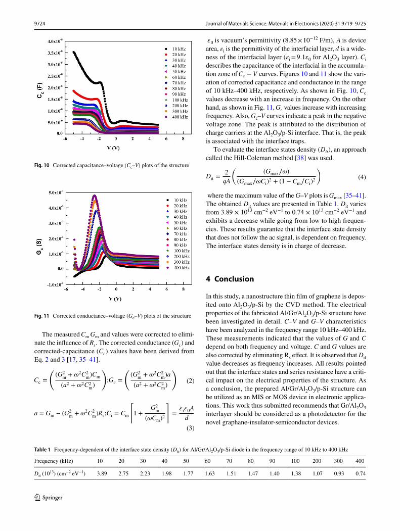
to ac voltage change at lower frequencies. The contribution of interface trap capacitance is negligibly small at high fre-quencies region. The total capacitance value is maximum at the accumulation region and C = Cins . For the depletion region, as the silicon capacitance increases by the formation of the depletion layer, the total capacitance decreases as they are in series with each other. Finally, for the inversion region, total capacitance is the series combination of insulator capacitance and inversion layer capacitance. Also, the C–V graphs give a peak in the depletion region. This is because interface states placed in the forbidden energy gap, existing of series resistance, doping concentration, and thickness of the interfacial insulator layer [18, 25–36]. Interface states are impressive in the depletion and inversion regions. As seen in Fig. 7, in contrast to C values, the measured G values increase with increasing frequency. Conductance (G = 1/R) is related to the R
s . The increase of G is due to the decrease
of Rs with increasing frequency.Usually, series resistance ( R
s ) in the semiconductor
devices corresponds to the contact resistances of the metal
electrodes. For this reason, it is an important parameter that cause a change in electrical features. To calculate the series resistance, the following relation is given as [25–36]:
where Gm (measured-conductance) and Cm (measured-capacitance) in the accumulation zone respectively. For different frequencies, Rs–V graphs are presented in Fig. 9. It is seen that the Rs weren’t dependent on the voltage at the positive bias and accumulation zone. Also, the Rs val-ues increase with decreasing frequency due to the interface charges dependent on the frequency. In obtaining frequency and voltage-dependent characteristics of the structure, Rs must be taken into consideration. Besides, Rs–V curves show a peak. The peak size increases with reducing the frequency and the position of peak shifts to the negative bias of zone from − 1 to 0 V. The peak behavior of R
s is the result of
interlayer/semiconductor interface traps under an external electric field or re-ordering and restructuring of charges at surface states or interface states at the interface. In this structure, Al2O3 used as an interlayer reduces the effect of chemically active dangling bonds at the surface of silicon, which eventually decreases the defects in graphene growth. Besides, passivating the surface with Al2O3 prevents thick native oxide formation at the interface. Therefore, the reduc-tion of defects in graphene on top of Al2O3 can decrease the series resistance of the device. Thus, Al2O3 layer contributed to improving the carrier lifetime for Si substrate decreasing the series resistance, reducing the surface recombination, and decreasing the density of traps significantly causing a major reduction in the surface recombination.
(1)Rs=
Gm
G2
m+ �2C2
m
Fig. 8 Conductance–voltage (G–V) plots of the Al/Gr/Al2O3/p-Si structure
Fig. 9 Series resistance–voltage (Rs–V) plots of the structure
9724 Journal of Materials Science: Materials in Electronics (2020) 31:9719–9725
1 3
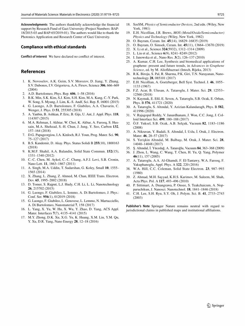
The measured Cm
Gm
and values were corrected to elimi-nate the influence of Rs . The corrected conductance ( Gc ) and corrected-capacitance ( Cc ) values have been derived from Eq. 2 and 3 [17, 35–41].
(2)Cc=
(
(G2
m+ �
2C2
m)C
m
(a2 + �2C2
m)
)
;Gc =
(
(G2
m+ �
2C2
m)a
(a2 + �2C2
m)
)
(3)
a = Gm− (G2
m+ �
2C2
m)R
s;C
i= C
m
[
1 +G2
m
(�Cm)2
]
=
�i�0A
d
�0 is vacuum’s permittivity (8.85 × 10⁻¹² F/m), A is device
area, εi is the permittivity of the interfacial layer, d is a wide-ness of the interfacial layer (εi = 9.1ε0 for Al2O3 layer). C
i
describes the capacitance of the interfacial in the accumula-tion zone of C
c− V curves. Figures 10 and 11 show the vari-
ation of corrected capacitance and conductance in the range of 10 kHz–400 kHz, respectively. As shown in Fig. 10, C
c
values decrease with an increase in frequency. On the other hand, as shown in Fig. 11, Gc values increase with increasing frequency. Also, G
c–V curves indicate a peak in the negative
voltage zone. The peak is attributed to the distribution of charge carriers at the Al2O3/p-Si interface. That is, the peak is associated with the interface traps.
To evaluate the interface states density ( Dit ), an approach called the Hill-Coleman method [38] was used.
where the maximum value of the G–V plots is Gmax
[35–41]. The obtained D
it values are presented in Table 1. D
it varies
from 3.89 × 1013 cm−2 eV−1 to 0.74 × 1013 cm−2 eV−1 and exhibits a decrease while going from low to high frequen-cies. These results guarantee that the interface state density that does not follow the ac signal, is dependent on frequency. The interface states density is in charge of decrease.
4 Conclusion
In this study, a nanostructure thin film of graphene is depos-ited onto Al2O3/p-Si by the CVD method. The electrical properties of the fabricated Al/Gr/Al2O3/p-Si structure have been investigated in detail. C–V and G–V characteristics have been analyzed in the frequency range 10 kHz–400 kHz. These measurements indicated that the values of G and C depend on both frequency and voltage. C and G values are also corrected by eliminating Rs effect. It is observed that D
it
value decreases as frequency increases. All results pointed out that the interface states and series resistance have a criti-cal impact on the electrical properties of the structure. As a conclusion, the prepared Al/Gr/Al2O3/p-Si structure can be utilized as an MIS or MOS device in electronic applica-tions. This work thus submitted recommends that Gr/Al2O3 interlayer should be considered as a photodetector for the novel graphane-insulator-semiconductor devices.
(4)Dit=
2
qA
(
(Gmax
∕�)
(Gmax
∕�Ci)2+ (1 − C
m∕C
i)2
)
Fig. 10 Corrected capacitance–voltage (Cc–V) plots of the structure
Fig. 11 Corrected conductance–voltage (Gc–V) plots of the structure
Table 1 Frequency-dependent of the interface state density (Dit) for Al/Gr/Al2O3/p-Si diode in the frequency range of 10 kHz to 400 kHz
Frequency (kHz) 10 20 30 40 50 60 70 80 90 100 200 300 400
Dit (1013) (cm−2 eV−1) 3.89 2.75 2.23 1.98 1.77 1.63 1.51 1.47 1.40 1.38 1.07 0.93 0.74
9725Journal of Materials Science: Materials in Electronics (2020) 31:9719–9725
1 3
Acknowledgments The authors thankfully acknowledge the financial support by Research Fund of Gazi University (Project Numbers: BAP-18/2015-03 and BAP-65/2019-01). The authors would like to thank the Photonics Application and Research Center of Gazi University.
Compliance with ethical standards
Conflict of interest We have declared no conflict of interest.
References
1. K. Novoselov, A.K. Geim, S.V. Morozov, D. Jiang, Y. Zhang, S.V. Dubonos, I.V. Grigorieva, A.A. Firsov, Science 306, 666–669 (2004)
2. A.D. Bartolomeo, Phys. Rep. 606, 1–58 (2016) 3. B.K. Min, S.K. Kim, S.J. Kim, S.H. Kim, M.A. Kang, C.-Y. Park,
W. Song, S. Myung, J. Lim, K.-S. Andf, Sci. Rep. 5, 16001 (2015) 4. G. Luongo, A.D. Bartolomeo, F. Giubileo, A.A. Chavarin, C.
Wenger, J. Phys. D 51, 255305 (2018) 5. A. Yanbin, B. Ashkan, P. Eric, B. Gijs, U. Ant, J. Appl. Phys. 118,
114307 (2015) 6. M.A. Rehman, I. Akhtar, W. Choi, K. Akbar, A. Farooq, S. Hus-
sain, M.A. Shehzad, S.-H. Chun, J. Jung, Y. Seo, Carbon 132, 157–164 (2018)
7. D.G. Papageorgiou, I.A. Kinloch, R.J. Youn, Prog. Mater. Sci. 90, 75–127 (2017)
8. B.S. Kandemir, D. Akay. Phys. Status Solidi B 255(10), 1800163 (2018)
9. K.M.F. Shahil, A.A. Balandin, Solid State Commun. 152(15), 1331–1340 (2012)
10. C.-C. Chen, M. Aykol, C.-C. Chang, A.F.J. Levi, S.B. Cronin, Nano Lett. 11, 1863–1867 (2011)
11. A. Singh, M.A. Uddin, T. Sudarshan, G. Koley, Small 10, 1555–1565 (2014)
12. X. Zhang, L. Zhang, Z. Ahmed, M. Chan, IEEE Trans. Electron. Dev. 65, 1995–2002 (2018)
13. D. Tomer, S. Rajput, L.J. Hudy, C.H. Li, L. Li, Nanotechnology 26, 215702 (2015)
14. G. Luongo, F. Giubileo, L. Iemmo, A. Di Bartolomeo, J. Phys.: Conf. Ser. 956(1), 012019 (2018)
15. G. Luongo, F. Giubileo, L. Genovese, L. Lemmo, N. Martucciello, A. Di Bartolomeo, Nanomaterial 7, 158 (2017)
16. L. Yang, X. Yu, W. Hu, X. Wu, Y. Zhao, D. Yang, ACS Appl. Mater. Interfaces 7(7), 4135–4141 (2015)
17. M.Y. Zhong, D.K. Xu, X.G. Yu, K. Huang, X.M. Liu, Y.M. Qu, Y. Xu, D.R. Yang, Nano Energy 28, 12–18 (2016)
18. SzeSM, Physics of Semiconductor Devices, 2nd edn. (Wiley, New York, 1981)
19. E.H. Nicollian, J.R. Brews, MOS (Metal/Oxide/Semiconductor) Physics and Technology (Wiley, New York, 1982)
20. O. Bayram, Ceram. Int. 45(14), 16829–16835 (2019) 21. O. Bayram, O. Simsek, Ceram. Int. 45(11), 13664–13670 (2019) 22. X. Li et al., Science 324(5932), 1312–1314 (2009) 23. L. Liu et al., Science 6(9), 8241–8249 (2012) 24. I. Janowska et al., Nano Res. 3(2), 126–137 (2010) 25. A. Kumar, C.H. Lee, Synthesis and biomedical applications of
graphene: present and future trends, in Advances in Graphene Science, ed. by M. Aliofkhazraei (Intech, Rijeka, 2013)
26. R.K. Biroju, S. Pal, R. Sharma, P.K. Giri, T.N. Narayanan, Nano-technology 28, 085101 (2017)
27. E.H. Nicollian, A. Goetzberger, Bell Syst. Technol. J. 46, 1055–1133 (1967)
28. F.Z. Acar, B. Ulusan, A. Tataroglu, J. Mater. Sci. 29, 12553–12560 (2018)
29. N. Kaymak, E. Efil, E. Seven, A. Tataroglu, S.B. Ocak, E. Orhan, Phys. B 576, 411721 (2020)
30. A. Tataroglu, S. Altındal, Y. Azizian-Kalandaragh, Phys. B 582, 411996 (2020)
31. V. Rajagopal Reddy, V. Janardhanam, J. Won, C.C. Jong, J. Col-loid Interface Sci. 499, 180–188 (2017)
32. Ö.F. Yuksel, S.B. Ocak, A.B. Selçuk, Vacuum 82, 1183–1186 (2008)
33. A. Nikravan, Y. Badali, S. Altındal, İ. Uslu, İ. Orak, J. Electron. Mater. 46, 28–57 (2017)
34. S. Yerişkin Altındal, M. Balbaşı, M. Orak, J. Mater. Sci. 28, 14040–14048 (2017)
35. Ş. Altındal, İ. Yücedağ, A. Tataroğlu, Vacuum 84, 363–368 (2009) 36. J. Zhou, L. Wang, C. Wang, T. Chen, H. Yu, Q. Yang, Polymer
46(11), 157 (2005) 37. A. Tataroglu, A.A. Al-Ghamdi, F. El-Tantawy, W.A. Farooq, F.
Yakuphanoglu, Appl. Phys. A 122, 220 (2016) 38. W.A. Hill, C.C. Coleman, Solid State Electron. 23, 987–993
(1980) 39. Z. Ahmad, M.H. Sayyad, K.H.S. Karimov, M. Saleem, M. Shah,
Acta Phys. Pol. A 117, 493–496 (2010) 40. P. Sittimart, A. Duangrawa, P. Onsee, S. Teakchaicum, A. Nop-
paruchikun, J. Nanosci. Nanotechnol. 18, 1841–1846 (2018) 41. C.H. Lee, S.H. Ryu, S.Y. Oh, J. Polym. Sci. B. 41, 2733–2743
(2003)
Publisher’s Note Springer Nature remains neutral with regard to jurisdictional claims in published maps and institutional affiliations.
Related Documents