1 RF Performance Projections of Graphene FETs vs. Silicon MOSFETs S. Rodriguez * , S. Vaziri * , M. Ostling * , A. Rusu * , E. Alarcon *,# , M.C. Lemme *1 * KTH Royal Institute of Technology, School of ICT, Kista, Sweden # UPC Universitat Politecnica de Catalunya, Barcelona, Spain Abstract—A graphene field-effect-transistor (GFET) model calibrated with extracted device parameters and a commercial 65 nm silicon MOSFET model are compared with respect to their radio frequency behavior. GFETs slightly lag behind CMOS in terms of speed despite their higher mobility. This is counterintuitive, but can be explained by the effect of a strongly nonlinear voltage-dependent gate capacitance. GFETs achieve their maximum performance only for narrow ranges of V DS and I DS , which must be carefully considered for circuit design. For our parameter set, GFETs require at least µ=3000 cm 2 V -1 s -1 to achieve the same performance as 65nm silicon MOSFETs. Index Terms—graphene FET (GFET), CMOS, RF 1 [email protected]

Welcome message from author
This document is posted to help you gain knowledge. Please leave a comment to let me know what you think about it! Share it to your friends and learn new things together.
Transcript
1
RF Performance Projections of Graphene FETs vs. Silicon MOSFETs
S. Rodriguez*, S. Vaziri*, M. Ostling*, A. Rusu*, E. Alarcon*,#, M.C. Lemme*1
*KTH Royal Institute of Technology, School of ICT, Kista, Sweden
#UPC Universitat Politecnica de Catalunya, Barcelona, Spain
Abstract—A graphene field-effect-transistor (GFET) model calibrated with
extracted device parameters and a commercial 65 nm silicon MOSFET model
are compared with respect to their radio frequency behavior. GFETs slightly lag
behind CMOS in terms of speed despite their higher mobility. This is
counterintuitive, but can be explained by the effect of a strongly nonlinear
voltage-dependent gate capacitance. GFETs achieve their maximum
performance only for narrow ranges of VDS and IDS, which must be carefully
considered for circuit design. For our parameter set, GFETs require at least
µ=3000 cm2 V-1 s-1 to achieve the same performance as 65nm silicon MOSFETs.
Index Terms—graphene FET (GFET), CMOS, RF
2
INTRODUCTION
Graphene has attracted enormous research interest in the solid state physics and
electronics communities since its experimental discovery in 2004.1 The unusual
electronic band structure of graphene with an energy band gap of 0 eV and a linear
dispersion relation leads to charge carriers with extremely high carrier mobilities,
with up to 10×103-15×103 cm2 V-1 s-1 reported for graphene on SiO2.2 A high
saturation velocity of >3×107 cm/s has been reported for low carrier densities.3
Finally, its two-dimensional structure allows the top-down fabrication of graphene
field effect transistors (GFETs) using silicon technology.4 However, due to the
absence of a band gap, GFETs are not favorable for logic circuits. On the other hand,
under certain DC biasing conditions, GFETs display current saturation, similar to
MOS and bipolar devices.5,6 These saturation regions are of particular interest for
analog circuit design as they enable GFETs to be used in amplifier configurations.
Furthermore, transit frequencies fT in excess of 100 GHz suggest GFETs for RF
applications.7,8 Nevertheless, it is still unclear how GFET technology at its present
state compares with nanometer CMOS in terms of high frequency circuit design
performance metrics.
This letter compares systematically the RF performance of current nanometer
CMOS technology and the performance of GFET technology, projected by scaling
critical dimensions in a model. The CMOS models used for this comparison belong to
a 65nm CMOS commercial process. The GFET model is based on our experimental
data to which the models of Meric et al.5 and Thiele et al.9 are applied. Key
parameters such as minimum sheet carrier concentration ρsh0, Dirac offset voltage VGS-
top0, carrier low field mobility µ, and saturation velocity vsat were extracted from
experiments and used to fit the model. This Drift-Diffusion model should accurately
3
describe transport at 65nm, as the extracted mobility indicates that fixed charge
impurities, charge puddles, substrate roughness and short range scattering centers
dominate the transport, which is in line with a channel length-independent saturation
velocity down to 130nm reported recently.10 For shorter devices, the ballisticity of
transport will become increasingly dominant, but given the variability in the graphene
and device manufacturing processes, a universal description is impossible at the
moment. We note that we have not included a model for contact resistance, but only a
contact resistance parameter based on.5 However, RF designs typically allow for
ample chip area for low resistance and high current densities in the devices. The
GFET model was implemented in Verilog AMS so that it can be simulated using the
same circuit design tools and setups as the commercial CMOS process. After
comparing the RF performance of the two technologies, a discussion about the impact
of µ on fT of GFET devices is presented. Finally, a prediction of fT for technologically
viable µ values is presented.
EXPERIMENT
Graphene FETs were fabricated on silicon wafers with 285 nm of thermal oxide.
Mechanical exfoliation was used to transfer the graphene onto the substrates. After
electron beam lithography, 30 nm of tungsten was deposited as source and drain
contacts. After evaporation of 30 nm of SiO2, the gate contact was defined by e-beam
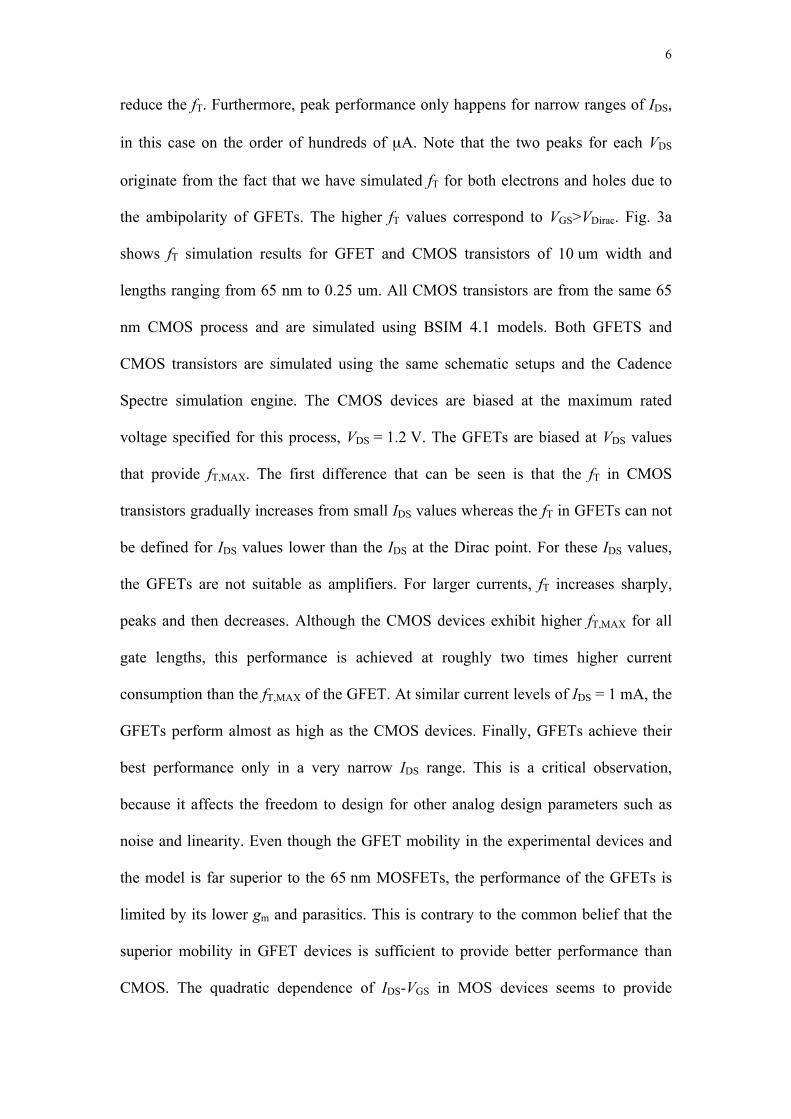
lithography and lift-off. The inset in Fig. 1a shows an optical micrograph of the
GFET, which has a channel length of L = 1 µm and a width of W = 10 µm. The IDS-
VGS measurement (lines) and fitted model (dotted lines) in Fig. 1a show the typical
ambipolar behavior of GFETs and a shift of the Dirac voltage (i.e. the point of
minimum conductance) with increasing drain voltage, which can be explained by the
influence of the drain voltage on the channel potential.6 This drain induced Dirac shift
4
(DIDS) is one reason for current saturation in the output characteristics. The extracted
parameters after fitting the measured data to the model are: minimum sheet carrier
concentration ρsh0 = 0.7×1012 cm-2, Dirac offset voltage VGS-top0 = 0.5 V, and carrier
low field mobility µ = 2500 cm2 V-1 s-1. The saturation velocity expression is taken
from Thiele et al.9:
( ) ( )xVsh
satv 2
21
21+
Ω=πρ
(1)
where V(x) is the voltage drop at each point in the graphene channel.
With these values extracted from the experimental data, the model allows us to
virtually scale the gate length to L = 65 nm and the oxide thickness to TOX = 2.6 nm.
These values correspond to those in the 65 nm CMOS process used for comparison.
Fig. 1b shows the simulated drain-source currents IDS as a function of gate-source
voltage VGS and drain-source voltage VDS for the scaled GFET. It can be seen that for
gate voltages smaller than the Dirac voltage, IDS increases similar to CMOS devices
operating in the triode region. As VGS becomes larger (i.e. more positive) than the
Dirac voltage, IDS saturates, making possible the design of different amplifying
blocks. Beyond VDS = 1V, the drain current increases again for increasing VDS, as
shown in 5 and 9. Since this is beyond the parameter space for the 65nm CMOS
reference used in this work (VDD = 1.2 V), we have not plotted this range.
MODEL-BASED PROJECTION OF RF PERFORMANCE METRICS
Typically, the performance of amplifying devices at high frequencies can be
compared by looking at the transit frequency fT, which can be expressed as:
tot
mT C
gfπ21
= (2)
where gm and Ctot represent the transconductance and total input capacitance. Ctot is

5
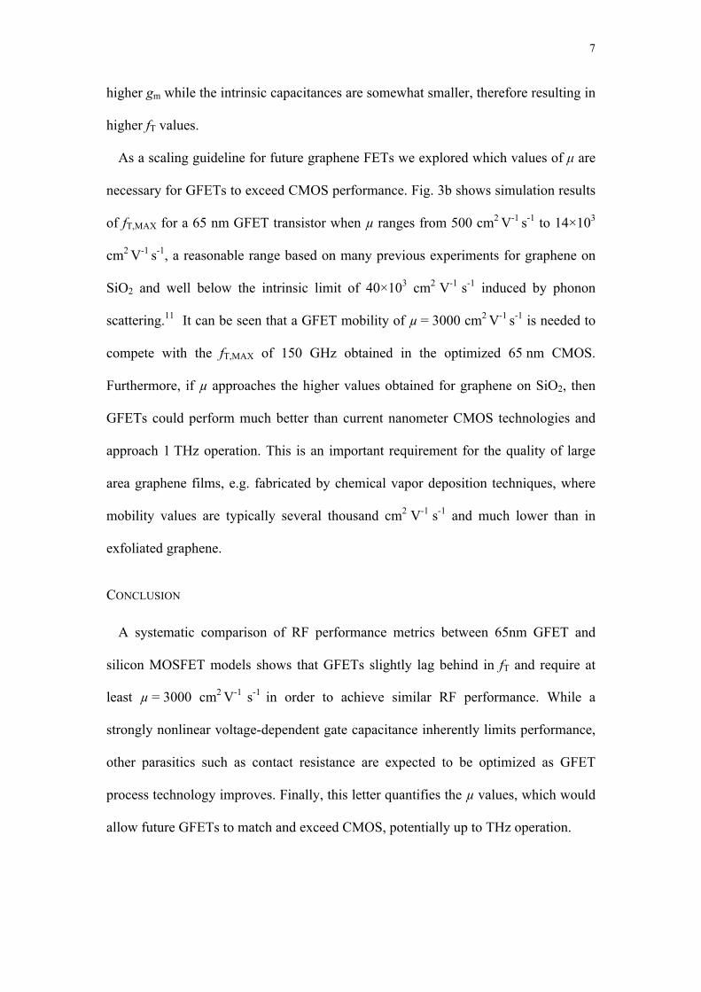
assumed to be dominated by the gate capacitance CG of the GFET. The effect of
overlap and fringing capacitances between gate-drain, and gate-source terminals are
more difficult to estimate since the contact resistances dominate at RF frequencies.
When these resistances are very high, these parasitic capacitors can be disregarded for
practical purposes. Although these extrinsic parasitic capacitances will reduce
somewhat the performance of the device, the intrinsic capacitance CG still dominates
and fundamentally limits the achievable fT.
The value of CG at each point of the channel is expressed as the series of the top gate
oxide capacitance Cox-top and the quantum capacitance Cq. Cox-top is constant whereas
Cq is a function of the voltage drop V at each point in the graphene channel. V is 0V at
the source, and VDS at the drain. The capacitance Cox-back is disregarded since it is
short-circuited by the DC source VGS-back. Accordingly, the total value of CG is
obtained by using the following expression:
( )( )∫ +
⋅=
−
−DSV
qtopox
qtopoxG dV
VCCVCC
WC
0 (3)
Fig. 2a shows the simulated values of CG for the 65 nm GFET. CG is strongly
dependent on VGS, with a minimum at the Dirac point. Similar to gm, CG also depends
strongly on VDS, which leads to a large variation in CG magnitude and has a profound
impact on the maximum speed of the transistor. This is quite opposite to CMOS
transistors, where the overlap capacitance CGD is independent of biasing voltages, and
CGS is relatively constant at the saturation region with an approximate value of
2/3COXWL. This situation can also be seen in Fig. 2b where the simulated fT is plotted
against IDS for different VDS voltages. It can be seen that the fT peaks for VDS of around
210mV and IDS of 1.25mA. We call it the fT,MAX of the device (not to be confused
with fMAX where the power gain becomes 1). Larger VDS voltages or IDS currents only
6
reduce the fT. Furthermore, peak performance only happens for narrow ranges of IDS,
in this case on the order of hundreds of µA. Note that the two peaks for each VDS
originate from the fact that we have simulated fT for both electrons and holes due to
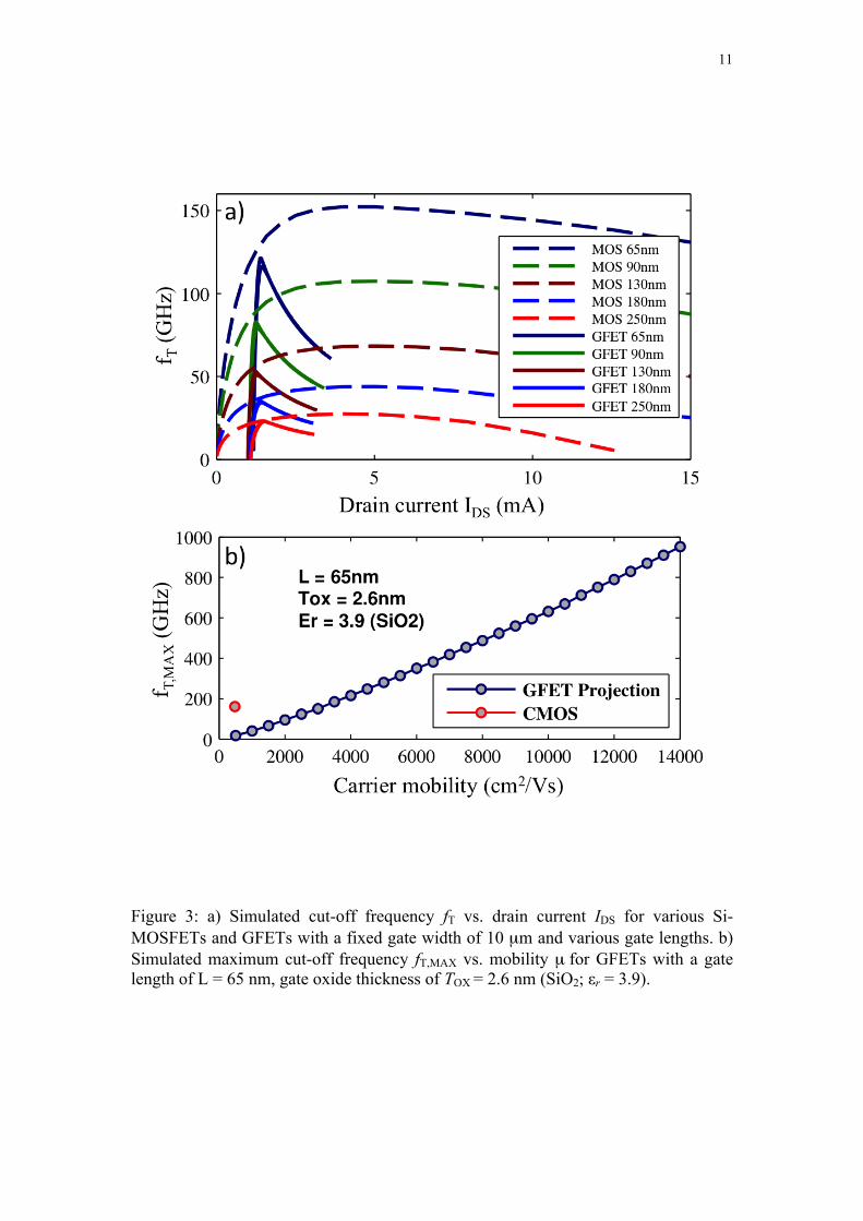
the ambipolarity of GFETs. The higher fT values correspond to VGS>VDirac. Fig. 3a
shows fT simulation results for GFET and CMOS transistors of 10 um width and
lengths ranging from 65 nm to 0.25 um. All CMOS transistors are from the same 65
nm CMOS process and are simulated using BSIM 4.1 models. Both GFETS and
CMOS transistors are simulated using the same schematic setups and the Cadence
Spectre simulation engine. The CMOS devices are biased at the maximum rated
voltage specified for this process, VDS = 1.2 V. The GFETs are biased at VDS values
that provide fT,MAX. The first difference that can be seen is that the fT in CMOS
transistors gradually increases from small IDS values whereas the fT in GFETs can not
be defined for IDS values lower than the IDS at the Dirac point. For these IDS values,
the GFETs are not suitable as amplifiers. For larger currents, fT increases sharply,
peaks and then decreases. Although the CMOS devices exhibit higher fT,MAX for all
gate lengths, this performance is achieved at roughly two times higher current
consumption than the fT,MAX of the GFET. At similar current levels of IDS = 1 mA, the
GFETs perform almost as high as the CMOS devices. Finally, GFETs achieve their
best performance only in a very narrow IDS range. This is a critical observation,
because it affects the freedom to design for other analog design parameters such as
noise and linearity. Even though the GFET mobility in the experimental devices and
the model is far superior to the 65 nm MOSFETs, the performance of the GFETs is
limited by its lower gm and parasitics. This is contrary to the common belief that the
superior mobility in GFET devices is sufficient to provide better performance than
CMOS. The quadratic dependence of IDS-VGS in MOS devices seems to provide
7
higher gm while the intrinsic capacitances are somewhat smaller, therefore resulting in
higher fT values.
As a scaling guideline for future graphene FETs we explored which values of µ are
necessary for GFETs to exceed CMOS performance. Fig. 3b shows simulation results
of fT,MAX for a 65 nm GFET transistor when µ ranges from 500 cm2 V-1 s-1 to 14×103
cm2 V-1 s-1, a reasonable range based on many previous experiments for graphene on
SiO2 and well below the intrinsic limit of 40×103 cm2 V-1 s-1 induced by phonon
scattering.11 It can be seen that a GFET mobility of µ = 3000 cm2 V-1 s-1 is needed to
compete with the fT,MAX of 150 GHz obtained in the optimized 65 nm CMOS.
Furthermore, if µ approaches the higher values obtained for graphene on SiO2, then
GFETs could perform much better than current nanometer CMOS technologies and
approach 1 THz operation. This is an important requirement for the quality of large
area graphene films, e.g. fabricated by chemical vapor deposition techniques, where
mobility values are typically several thousand cm2 V-1 s-1 and much lower than in
exfoliated graphene.
CONCLUSION
A systematic comparison of RF performance metrics between 65nm GFET and
silicon MOSFET models shows that GFETs slightly lag behind in fT and require at
least µ = 3000 cm2 V-1 s-1 in order to achieve similar RF performance. While a
strongly nonlinear voltage-dependent gate capacitance inherently limits performance,
other parasitics such as contact resistance are expected to be optimized as GFET
process technology improves. Finally, this letter quantifies the µ values, which would
allow future GFETs to match and exceed CMOS, potentially up to THz operation.

8
ACKNOWLEDGEMENT
The authors gratefully acknowledge support through an Advanced Investigator
Grant (OSIRIS, No. 228229) and a Starting Grant (InteGraDe, No. 307311) from the
European Research Council.
9
FIGURES
Figure 1: a) Measured (solid lines) and modeled (dashed lines) transfer characteristics of a GFET with a gate width of W=10 µm and a gate length of L = 1 µm used as the basis for this work. Inset: Optical microscope image of the device (false color). b) Modeled drain current IDS for different VGS and VDS bias conditions for virtually scaled GFET with L = 65 nm and W = 10 µm.
10
Figure 2: a) Top gate capacitance CG vs. gate voltage VGS for various drain bias voltages VDS. b) Cut-off frequency fT vs. drain current IDS for various drain bias voltages VDS. (L = 65 nm and W = 10 µm).
11
Figure 3: a) Simulated cut-off frequency fT vs. drain current IDS for various Si-MOSFETs and GFETs with a fixed gate width of 10 µm and various gate lengths. b) Simulated maximum cut-off frequency fT,MAX vs. mobility µ for GFETs with a gate length of L = 65 nm, gate oxide thickness of TOX = 2.6 nm (SiO2; εr = 3.9).
12
REFERENCES
1. K. S. Novoselov, A. K. Geim, S. V. Morozov, D. Jiang, Y. Zhang, S. V. Dubonos, I. V. Grigorieva, and A. A. Firsov, Science, 306, 666-669 (2004).
2 Y. Zhang, Y.-W. Tan, H. L. Stormer, and P. Kim, Nature, 438, 201-204 (2005).
3 V. E. Dorgan, M.-H. Bae, and E. Pop, Applied Physics Letters, vol. 97, 082112 (2010).
4 M. C. Lemme, T. J. Echtermeyer, M. Baus, and H. Kurz, IEEE Electron Device Letters, 28, 282-284 (2007).
5 I. Meric, M. Y. Han, A. F. Young, B. Ozyilmaz, P. Kim, and K. L. Shepard, Nat Nano, 3, 654-659 (2008).
6 S. J. Han, Z. Chen, A. A. Bol, and Y. Sun, IEEE Electron Device Letters, 32, 812-814 (2011).
7 Y. M. Lin, C. Dimitrakopoulos, K. A. Jenkins, D. B. Farmer, H. Y. Chiu, A. Grill, and P. Avouris, Science, 327, 662 (2010).
8 L. Liao, Y.-C. Lin, M. Bao, R. Cheng, J. Bai, Y. Liu, Y. Qu, K. L. Wang, Y. Huang, and X. Duan, Nature, 467, 305-308 (2010).
9 S. A. Thiele, J. A. Schaefer, and F. Schwierz, Journal of Applied Physics, 107 (2010).
10 I. Meric, C. R. Dean, A. F. Young, N. Baklitskaya, N. J. Tremblay, C. Nuckolls, P. Kim, and K. L. Shepard, Nano Letters, 11, 1093-1097 (2011).
11 J.-H. Chen, C. Jang, S. Xiao, M. Ishigami, and M. S. Fuhrer, Nat Nano, 3, 206-209 (2008).
Related Documents