Semiconductor to metal transition in bilayer phosphorene under normal compressive strain Aaditya Manjanath †,‡,¶ , Atanu Samanta †,¶ ,Tribhuwan Pandey †,¶ and Abhishek K. Singh † † Materials Research Centre, Indian Institute of Science, Bangalore 560012, India ‡ Centre for Nano Science and Engineering, Indian Institute of Science, Bangalore 560012, India ¶ These authors contributed equally to this work E-mail: [email protected] Abstract. Phosphorene, a two-dimensional (2D) analog of black phosphorous, has been a subject of immense interest recently, due to its high carrier mobilities and a tunable bandgap. So far, tunability has been predicted to be obtained with very high compressive/tensile in-plane strains, and vertical electric field, which are difficult to achieve experimentally. Here, we show using density functional theory based calculations the possibility of tuning electronic properties by applying normal compressive strain in bilayer phosphorene. A complete and fully reversible semiconductor to metal transition has been observed at ∼ 13.35% strain, which can be easily realized experimentally. Furthermore, a direct to indirect bandgap transition has also been observed at ∼ 3% strain, which is a signature of unique band-gap modulation pattern in this material. The absence of negative frequencies in phonon spectra as a function of strain demonstrates the structural integrity of the sheets at relatively higher strain range. The carrier mobilities and effective masses also do not change significantly as a function of strain, keeping the transport properties nearly unchanged. This inherent ease of tunability of electronic properties without affecting the excellent transport properties of phosphorene sheets is expected to pave way for further fundamental research leading to phosphorene-based multi-physics devices. PACS numbers: 71.15.Mb, 71.20.Mq, 71.15.-m Submitted to: Nanotechnology

Welcome message from author
This document is posted to help you gain knowledge. Please leave a comment to let me know what you think about it! Share it to your friends and learn new things together.
Transcript
Semiconductor to metal transition in bilayer
phosphorene under normal compressive strain
Aaditya Manjanath†,‡,¶, Atanu Samanta†,¶,Tribhuwan Pandey†,¶
and Abhishek K. Singh†
†Materials Research Centre, Indian Institute of Science, Bangalore 560012, India‡Centre for Nano Science and Engineering, Indian Institute of Science, Bangalore
560012, India¶These authors contributed equally to this work
E-mail: [email protected]
Abstract. Phosphorene, a two-dimensional (2D) analog of black phosphorous, has
been a subject of immense interest recently, due to its high carrier mobilities and
a tunable bandgap. So far, tunability has been predicted to be obtained with
very high compressive/tensile in-plane strains, and vertical electric field, which
are difficult to achieve experimentally. Here, we show using density functional
theory based calculations the possibility of tuning electronic properties by applying
normal compressive strain in bilayer phosphorene. A complete and fully reversible
semiconductor to metal transition has been observed at ∼ 13.35% strain, which can be
easily realized experimentally. Furthermore, a direct to indirect bandgap transition
has also been observed at ∼ 3% strain, which is a signature of unique band-gap
modulation pattern in this material. The absence of negative frequencies in phonon
spectra as a function of strain demonstrates the structural integrity of the sheets at
relatively higher strain range. The carrier mobilities and effective masses also do not
change significantly as a function of strain, keeping the transport properties nearly
unchanged. This inherent ease of tunability of electronic properties without affecting
the excellent transport properties of phosphorene sheets is expected to pave way for
further fundamental research leading to phosphorene-based multi-physics devices.
PACS numbers: 71.15.Mb, 71.20.Mq, 71.15.-m
Submitted to: Nanotechnology
Semiconductor to metal transition in bilayer phosphorene under normal compressive strain2
1. Introduction
The experimental exfoliation of many-layer phosphorene [1, 2, 3] has garnered immense
interest, due to the presence of a direct bandgap [3, 4] and high carrier mobilities
(∼ 1000 cm2V−1s−1) [1], making it a potential candidate for nanoelectronic devices.
Within a phosphorene sheet, every phosphorous atom is covalently bonded with three
neighboring atoms forming a highly corrugated honeycomb-like structure. These sheets
are bonded by van der Waals (vdW) interactions in multi-layered phosphorene. In
order to widen the range of applications of phosphorene, it is necessary to engineer the
bandgap. It has been shown theoretically, that phosphorene exhibits strain-dependent
electronic properties [5]. The in-plane strain leads to a direct to indirect bandgap (D-I)
transition at very high tensile/compressive strains [5]. In addition, a normal compression
of monolayer phosphorene also leads to modulation of electronic structure [6].
The bandgap tunability study has also been extended to bilayer and many-layer
phosphorene. For example, the bandgap varies very strongly with the number of layers,
with a range of ∼ 2 eV (monolayer) to 0.3 eV (bulk) [7, 8]. It has been recently reported
that the bandgap in bilayer phosphorene can be modulated by changing the stacking
order or by applying a vertical electric field [9]. Experimentally, applying an electric
field on such a system is difficult because the fields required are large (∼ 0.5 V/A) [9].
Another way of modulating the bandgap could be by application of experimentally
feasible normal compressive (NC) strain, which is easiest to achieve due to relatively
weaker vdW interlayer interactions as shown for other 2D-layered materials [10, 11, 12].
Here, we show, using density functional calculations, the bandgap variation as a function
of NC strain. Reversible direct to indirect and semiconductor to metal transitions, occur
at applied NC strains of 3.32% and 13.35%, respectively. In addition, we find significant
anisotropy in the carrier mobilities and effective mass along x- and y-directions, which
do not change much with the NC strain, thereby maintaining the excellent transport
properties. Phonon spectra as a function of NC strain shows no instabilities, maintaining
structural and mechanical integrity even at very high compressions. Furthermore,
Raman frequency shift in A1g, B2g, and A2g as a function of applied strain were mapped
out, which will also help to monitor the bandgap modulation experimentally.
2. Methodology
The calculations were performed using first-principles density functional theory
(DFT) [13] as implemented in the Vienna ab initio simulation package (VASP) [14, 15].
The layers in phosphorene are held together by vdW forces, which is incorporated
by adding a semi-empirical dispersion potential (D) to the conventional Kohn-
Sham DFT energy, through a pair-wise force field following Grimme’s DFT-D3
method [16]. Projector augmented wave (PAW) [17, 18] pseudopotentials were used
for the electron-ion interactions. The exchange and correlation part of the total energy
was approximated by the generalized gradient approximation (GGA) using Perdew-
Semiconductor to metal transition in bilayer phosphorene under normal compressive strain3
4 6 8
Strain (%)
−4.6
−4.4
−4.2
−4.0
Eb
an
d−E
va
cu
um (
eV
)
VBM (at Γ)
CB (at Γ)CB (Γ→Y)
0 2
(e)
(b)
(c)
(d)Γ Γ X
−2
0
2
0
2
0
2
px
py
pz
E−E
F (
eV
)
DOS (a.u)
ε = 0%
ε = 3.32%
ε = 7.47%
Total
YM
−2
−2
ld
(a)
VBM
VB1
CBMCB1
k1
Figure 1. a) The crystal structure of bilayer phosphorene, d and l are the interlayer
distances measured with respect to inner and outer atoms, respectively. Band structure
and DOS of AB stacked phosphorene at b) 0% c) 3.32%, and d) 7.47% normal
compression, are shown. e) The change in VBM and CBM with strain.
Burke-Ernzerhof (PBE) type of functional [19]. Bilayer phosphorene has been predicted
to exist in three different stacking, namely AA, AB, and AC. The AB-stacked structure
is energetically the most preferred, and therefore, we carry out the rest of the study
on this. The unit cell consists of eight atoms as shown in Fig. 1(a) and Fig. S1, with
an optimum interlayer distance of d = 3.23 A. A vacuum of 27 A is included along the
z-axis to avoid spurious interactions between the periodic images. The Brillouin zone
was sampled with a well-converged Gamma-centered k-mesh of 17× 15× 1.
NC strain on this system was modelled by fixing the bottom layer and varying
the z co-ordinates of the atoms belonging to the top layer. A constrained structural
relaxation was performed using the conjugate-gradient method until the absolute value
of the components of forces were converged to within 0.005 eV/A. Phonon dispersions
and the Raman active modes were obtained from density functional perturbation theory
(DFPT) [20] with a strict energy convergence criterion of 1×10⁻⁸ eV in order to obtain
accurate forces. The Raman spectra were obtained by the linear response theory as
implemented in Quantum Espresso package [21].

Semiconductor to metal transition in bilayer phosphorene under normal compressive strain4
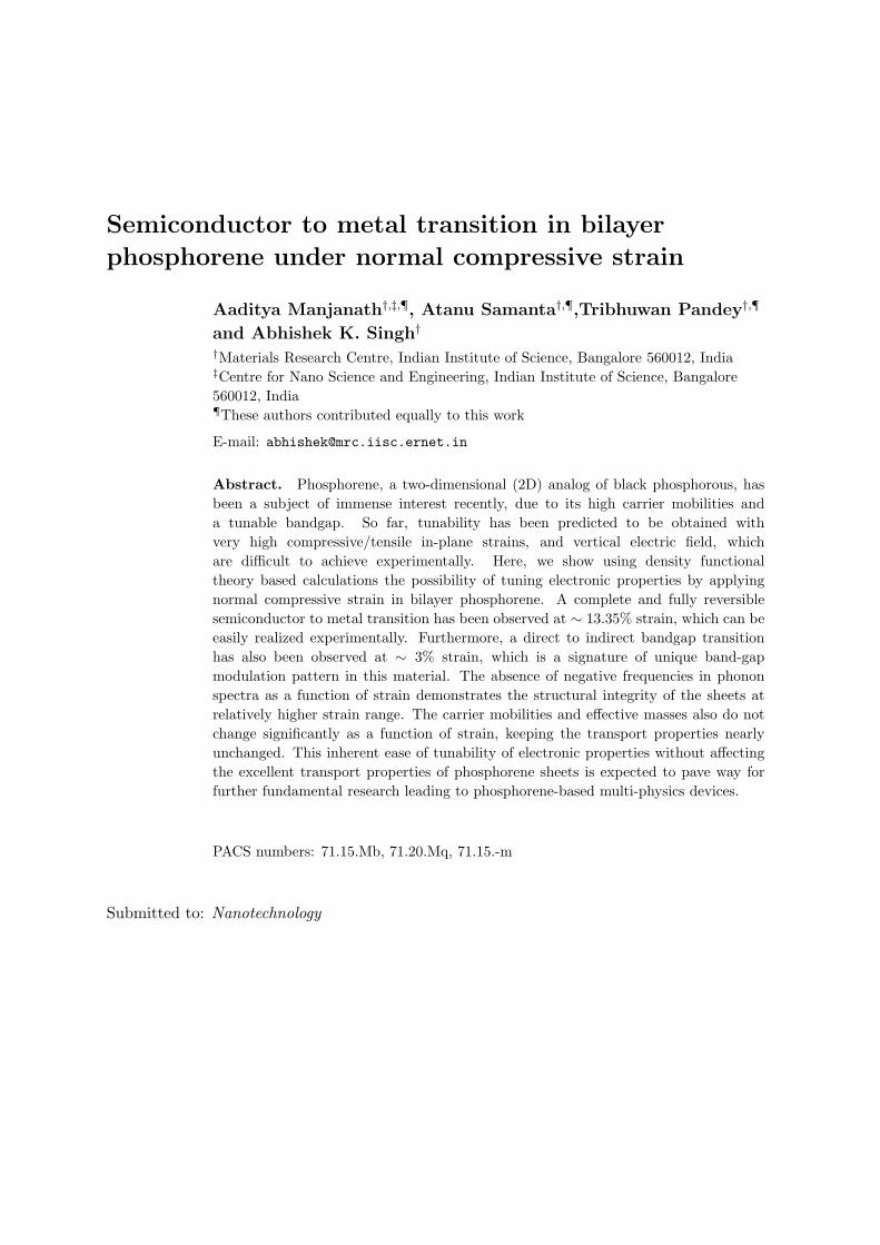
Figure 2. (a) Left panel shows band-decomposed charge densities corresponding to
VBM, VB1, and CBM at 0%, and right panel, VBM and CBM at 7.47% strain, as
viewed in the y-z plane. (b) The band-decomposed charge density of CB1 at 0, 3.32
and 7.47% strains, respectively as viewed in the x-z plane. All are plotted with the
same isosurface value.
3. Results and Discussion
Fig. 1 (a) shows AB bilayer phosphorene crystal structure. The calculated optimized
structural parameters using PBE including vdW interactions are shown in Table ST1,
which are in good agreement with the previously reported results [7]. The NC strain
was calculated as ǫ = (l− l0)/l0, where l0 and l are the equilibrium and strained layered
distance (Fig. 1(a)), respectively. The bond lengths δ1 and δ2 remain nearly unchanged
over the entire range of strain values. The changes in the structural parameters under
application of NC strain are shown in Fig. S1 (a), (b), and (c). There are no significant
changes in α′1, α2, and α′
2 observed with applied NC strain. The intralayer in-plane
angle α1 (as shown in Fig. S1 (c)) shows relatively larger changes indicating that NC
also enhances intralayer interactions.
Next we study the effect of NC strain on the electronic properties of bilayer
phosphorene. The PBE band structure calculations show that the unstrained AB
stacked bilayer phosphorene has a direct bandgap at Γ point of 0.48 eV. In comparison to
monolayer, the bandgap of bilayer phosphorene is 0.33 eV lower and shows two additional
Semiconductor to metal transition in bilayer phosphorene under normal compressive strain5
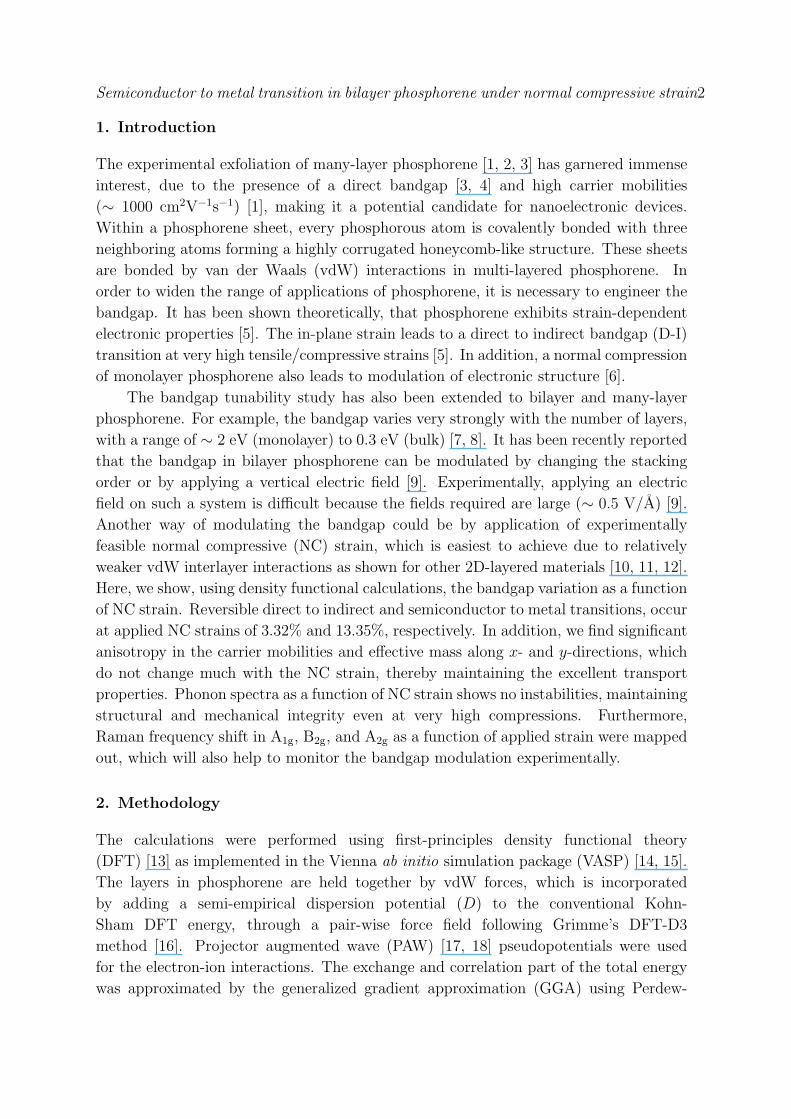
120.0
0.5
1.0
1.5
Eg (
eV
)
HSEPBEG
0W
0
(Γ-Γ
)
(Γ→Y)
4 8Strain (%)
0
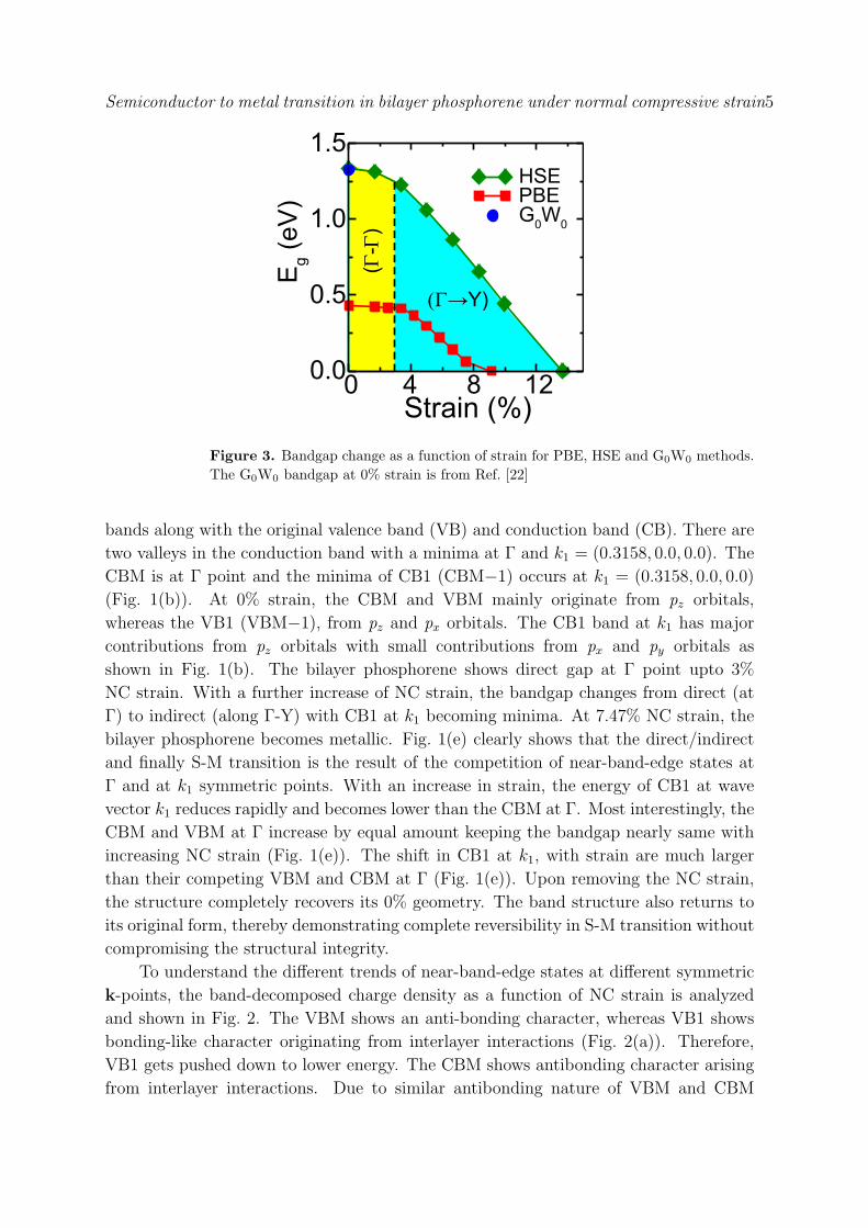
Figure 3. Bandgap change as a function of strain for PBE, HSE and G0W0 methods.
The G0W0 bandgap at 0% strain is from Ref. [22]
bands along with the original valence band (VB) and conduction band (CB). There are
two valleys in the conduction band with a minima at Γ and k1 = (0.3158, 0.0, 0.0). The
CBM is at Γ point and the minima of CB1 (CBM−1) occurs at k1 = (0.3158, 0.0, 0.0)
(Fig. 1(b)). At 0% strain, the CBM and VBM mainly originate from pz orbitals,
whereas the VB1 (VBM−1), from pz and px orbitals. The CB1 band at k1 has major
contributions from pz orbitals with small contributions from px and py orbitals as
shown in Fig. 1(b). The bilayer phosphorene shows direct gap at Γ point upto 3%
NC strain. With a further increase of NC strain, the bandgap changes from direct (at
Γ) to indirect (along Γ-Y) with CB1 at k1 becoming minima. At 7.47% NC strain, the
bilayer phosphorene becomes metallic. Fig. 1(e) clearly shows that the direct/indirect
and finally S-M transition is the result of the competition of near-band-edge states at
Γ and at k1 symmetric points. With an increase in strain, the energy of CB1 at wave
vector k1 reduces rapidly and becomes lower than the CBM at Γ. Most interestingly, the
CBM and VBM at Γ increase by equal amount keeping the bandgap nearly same with
increasing NC strain (Fig. 1(e)). The shift in CB1 at k1, with strain are much larger
than their competing VBM and CBM at Γ (Fig. 1(e)). Upon removing the NC strain,
the structure completely recovers its 0% geometry. The band structure also returns to
its original form, thereby demonstrating complete reversibility in S-M transition without
compromising the structural integrity.
To understand the different trends of near-band-edge states at different symmetric
k-points, the band-decomposed charge density as a function of NC strain is analyzed
and shown in Fig. 2. The VBM shows an anti-bonding character, whereas VB1 shows
bonding-like character originating from interlayer interactions (Fig. 2(a)). Therefore,
VB1 gets pushed down to lower energy. The CBM shows antibonding character arising
from interlayer interactions. Due to similar antibonding nature of VBM and CBM

Semiconductor to metal transition in bilayer phosphorene under normal compressive strain6
(interlayer interaction), energy of these states increase nearly equally with increasing
NC strain. However, CB1 has bonding feature due to interlayer interactions, which
mainly originates from pz orbitals. With increasing NCS the interlayer distance decrease,
which leads to increase in the overlap of pz orbitals between two layers and lowering the
energy of CB1. Due to this increase of interlayer interaction the CB1 becomes much
more dispersive. At the S-M transition NC strain of 7.47%, the density of states at
Fermi energy arises from phosphorous pz orbitals, as shown Fig. 1(d). This indicates
that the strong interlayer interaction of pz orbitals leads to S-M transition.
It is well-known that DFT with standard exchange-correlation functionals such
as the local-density approximation (LDA) or the generalized gradient approximation
(GGA) underestimates the bandgap of semiconductors [23, 24]. The PBE bandgap
of bilayer phosphorene is significantly lower than the experimentally reported
photoluminescence (PL) and G0W0 values of 1.3 eV [8] and 1.32 eV [22], respectively.
Therefore, it is very difficult to predict accurate strain dependence of electronic
properties within PBE. In order to correct the PBE bandgaps, we used a hybrid Heyd-
Scuseria-Ernzerhof (HSE06) [25, 26, 27, 28] functional. The functional is separated into a
long-range and a short-range part with 1/4 of the PBE exchange replaced by the Hartree-
Fock exact exchange and contains the full PBE correlation energy. The HSE06 generally
corrects the bandgap underestimation problem by partially removing the self interaction.
Previous studies have shown that the hybrid-functional HSE06 method shows significant
improvement of bandgap of mono- and multi-layer phosphorene [7, 22, 29]. Our HSE06
calculations at 0% strain with a mixing parameter of 0.35 show a bandgap of 1.33 eV,
which is in excellent agreement with G0W0 value [22] (Fig. 3). The dispersion of the
valence band does not change with respect to PBE. However, the conduction band
shifts upwards without significant change in the band dispersion (Fig. S2). Under
NC strain, similar changes in bandgap are observed as shown in Fig. 3. However, due
to a larger bandgap, S-M transition occurs at a higher strain value of 13.35% which
can also be achieved experimentally. Similar to PBE, the S-M transition in this case
was completely reversible. Interestingly, even at 0% strain, the interlayer interaction
reduces the bandgap (≈ 0.67 eV) compared to monolayer. This bandgap reduction is
much higher than the other vdW-layer materials [10]. Thus, interlayer interaction is an
important and dominating parameter, which can be modified by applying the NC strain
to tune the bandgap of bilayer phosphorene.
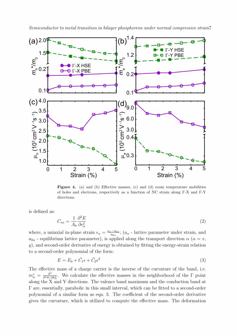
Since phosphorene exhibits excellent transport properties, it is important to study
the effect of NC strain on carrier effective masses and mobilities as the electronic
properties are governed by these. We assume that the mechanism limiting the mobility
of charge carriers is the scattering due to only longitudinal acoustic phonons [30, 31].
The carrier mobility in a 2D system is given by [7]:
µα =e~3Csα
kBTm∗α
√
m∗αm
∗βE
21α
(1)
where, Csα, m∗α, T and E1α are the in-plane stiffness, effective mass of the charge carrier
(hole/electron), temperature and the deformation potential along the αth direction. Csα
Semiconductor to metal transition in bilayer phosphorene under normal compressive strain7
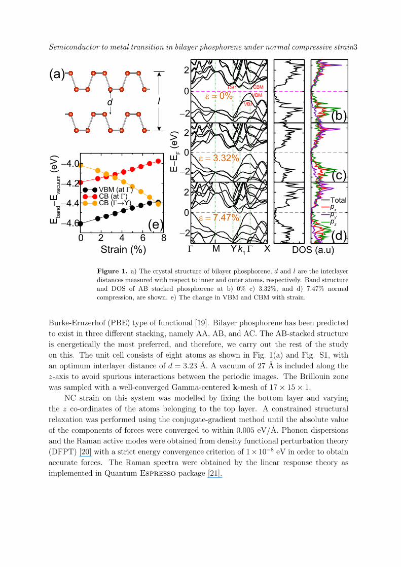
(a) (b)
(c) (d)
Strain (%)
0.1
0.2Γ-X HSEΓ-X PBE
Strain (%)
0.1
0.2
1.5
2.0
Γ-Y HSEΓ-Y PBE1.2
1.4m
h*/m
0
me*/m
0
1.0
1.5
2.0
2.5
3.0
3.5
4.0
µh (
10
3 c
m2
V -
1s
-1)
0.3
0.4
3.0
6.0
9.0
µe (
10
3 c
m2
V -
1s
-1)
0 1 2 3 4 5 0 1 2 3 4 5
Figure 4. (a) and (b) Effective masses, (c) and (d) room temperature mobilities
of holes and electrons, respectively as a function of NC strain along Γ-X and Γ-Y
directions.
is defined as:
Csα =1
A0
∂2E
∂ǫ2α(2)
where, a uniaxial in-plane strain ǫα = aα−a0αa0α
; (aα - lattice parameter under strain, and
a0α - equilibrium lattice parameter), is applied along the transport direction α (α = x,
y), and second-order derivative of energy is obtained by fitting the energy-strain relation
to a second-order polynomial of the form:
E = E0 + C1ǫ+ C2ǫ2 (3)
The effective mass of a charge carrier is the inverse of the curvature of the band, i.e.
m∗α = ~2
∂2E/∂k2α. We calculate the effective masses in the neighborhood of the Γ point
along the X and Y directions. The valence band maximum and the conduction band at
Γ are, essentially, parabolic in this small interval, which can be fitted to a second-order
polynomial of a similar form as eqn. 3. The coefficient of the second-order derivative
gives the curvature, which is utilized to compute the effective mass. The deformation
Semiconductor to metal transition in bilayer phosphorene under normal compressive strain8
potential is the change in the potential as a consequence of the applied in-plane strain,
which is defined as: E1α = ∆Vi
∆aα/a0α, where, ∆Vi is the change in the energy of the ith
band under in-plane strain. All the parameters have been obtained within the PBE
framework.
The parameters that markedly influence the mobility are the deformation potential
E1, the effective masses and the in-plane stiffness Cs. We analyze the effect of normal
compression on each of these parameters in addition to the mobility. Figs. 4(a) and (b)
show the effective masses of holes and electrons along the Γ-X (violet solid lines in Fig. 4)
and Γ-Y (green dashed lines in Fig. 4) directions, as a function of normal compression.
The effective masses have been calculated using both PBE (unfilled symbols in Fig. 4)
and HSE06 functionals (filled symbols in Fig. 4) to understand the effect of bandgap
underestimation. The PBE values of the effective masses are in good agreement in
terms of the order of magnitude with the HSE06 ones. In addition, the trends of the
effective masses are the same for both PBE and HSE06. Hence, qualitatively and to some
extent, quantitatively, PBE is sufficient to analyze the transport properties. For both
holes (Fig. 4(a)) and electrons (Fig. 4(b)), the effective masses along the Γ-Y direction
are significantly higher than those along Γ-X, implying a high anisotropy in the system.
On application of NC strain, the effective masses along Γ-Y (Γ-X) decrease (increase).
The reason for this increase/decrease can be attributed to the decrease/increase in the
curvature of the bands caused by the decrease/increase in the overlap of the bonding
(holes)/antibonding (electrons) orbitals.
The in-plane stiffness, Csx and Csy along the x- and y-directions, respectively, were
calculated according to the methodology described in our previous work [32]. Although
the values do not vary significantly with NC strain, overall, the Csx < Csy (Table S2),
implying anisotropy in the elastic properties. The trend is similar to that observed
in monolayer phosphorene [5]. Fig. S3(a) shows, the variation in total energy with
respect to in-plane strain for a given normal compression. The high curvature in the
energy surface for ǫy, suggests that it is difficult to apply strain along the y-direction
compared to x, also indicating that Csy is higher compared to Csx. In contrast to this,
the trends are different in the case of the deformation potentials (Fig. S4) depending on
the charge carrier under consideration (Table S2). The values as a function of normal
compression and the band-decomposed charge density plots for a given compression are
included in Figs. S3(b)-(e). With respect to holes, the VB wavefunction along y is
slightly more localized compared to x-direction. Therefore, any structural deformations
due to longitudinal phonons along this direction will affect the VB wavefunction lesser
compared to x-direction, thereby leading to E1y being lower than E1x. When comparing
the deformation potentials of holes and electrons along a particular direction, we find
contrasting trends, i.e. Eholes1x > Eelectrons
1x and Eholes1y < Eelectrons
1y , which are once again,
well explained by the band-decomposed charge density plots in Figs. S3(b)-(e). By
utilizing the trends described into equation 1, we find that for a given charge carrier,
µx > µy, whereas, along a particular direction, the relationships are µelectronsx > µholes
x ,
µelectronsy < µholes
y . Hence, the overall trends in mobilities (Table S2) are controlled by
Semiconductor to metal transition in bilayer phosphorene under normal compressive strain9
the trends in effective masses and deformation potentials. The mobilities do not change
significantly as a function of NC strain. Therefore, the transport properties of bilayer
phosphorene are preserved, despite the application of NC strain.
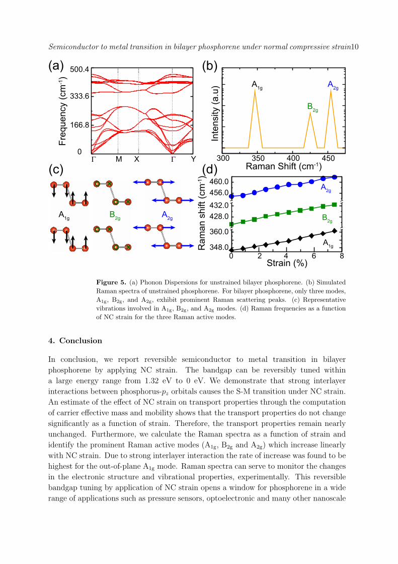
To explore the structural integrity of bilayer phosphorene under NC strain, phonon
calculations were performed. The symmetry of bilayer phosphorene is described by
the D2h point group. Fig. 5(a) shows the calculated phonon dispersion of bilayer-
phosphorene, which has 24 phonon branches. The optical branches have small splitting
and are nearly double degenerate due to the weak interlayer interaction. From Fig. 5(a),
we can see that there is no imaginary frequency in the full phonon spectra, indicating the
dynamical stability of bilayer phosphorene. This conclusion is in good agreement with
experiments, where it is shown that the exfoliated flakes of black phosphorous are stable
even in free-standing form [33]. The phonon dispersion calculation as a function of strain
indicates the dynamical stability of bilayer phosphorene even at high strains (Fig. S5).
At a very high strain of ∼ 15% small instability appear in the phonon dispersion, which
is well above the critical strain (the strain at which S-M transition occurs) predicted
by PBE or HSE06. Based on this analysis we conclude that the electronic properties of
bilayer phosphorene can be tuned efficiently and reversibly under a large strain window
while maintaining structural integrity.
The key changes in lattice vibrational modes as a function of NC strain can be
captured by Raman spectra [11]. We calculate the Raman spectra as a function of NC
strain as shown in Fig. 5(b) and Fig. S6. Here, only three modes, A1g, B2g, and A2g,
exhibit prominent Raman scattering peaks. The out-of-plane A1g mode occurs due to
opposing vibrations of top and bottom P atoms with respect to each other within the
same layer. The B2g and A2g mode is associated with the in-plane vibration of the P
atoms in directions opposite to one another as shown in Fig. 5(c). As shown in Fig. 5(b)
these peaks are located at 346.95, 425.62, and 454.63 cm−1 for unstrained phosphorene,
which are in good agreement with the reported experimental values [34, 3]. The strain
dependence of the three most prominent Raman active modes (one out-of-plane (A1g)
and two in-plane (B2g and A2g)) is shown in Fig. 5(d). While all the three different
modes show qualitatively, the same behavior with respect to applied strain and exhibit
a linear increase (blue shift), the rate of increase is different for different modes. The
A1g mode increases at a rate of 2.04 cm−1/∆ǫ and exhibits the highest blue shift of
∼ 15cm−1 under the strain range investigated here. The other two modes B2g and A2g
also increase linearly but with a lower rate of 0.95 and 0.96 cm−1/∆ǫ, respectively. The
different rate of increase of Raman active modes can be explained by analyzing the
type of vibrations involved in these modes. The A1g mode emerges from out-of-plane
vibrations of phosphorus atoms and has a strong dependence on interlayer distance. The
NC strain reduces the interlayer distance leading to a strong blue shift in the A1g mode,
whereas the B2g and A2g modes arise from the in-plane vibrations of phosphorus atoms
and hence experience lower shifts. Therefore, the Raman spectra and its trend with
respect to NC strain can be an effective way of monitoring the changes in the electronic
structure and lattice virations in bilayer phosphorene, experimentally.
Semiconductor to metal transition in bilayer phosphorene under normal compressive strain10
Γ M X Γ Y0
166.8
333.6
500.4F
req
ue
ncy (
cm
-1)
×
×
×
×
(a) (b)
(c) (d) Raman Shift (cm-1)
A1g
B2g
A2g
348.0
360.0
456.0
460.0
428.0
432.0R
am
an
sh
ift (c
m-1)
Strain (%)
A2g
B2g
A1g
0 2 4 6 8
300 350 400 450
Inte
nsity (
a.u
) A1g
A2g
B2g
Figure 5. (a) Phonon Dispersions for unstrained bilayer phosphorene. (b) Simulated
Raman spectra of unstrained phosphorene. For bilayer phosphorene, only three modes,
A1g, B2g, and A2g, exhibit prominent Raman scattering peaks. (c) Representative
vibrations involved in A1g, B2g, and A2g modes. (d) Raman frequencies as a function
of NC strain for the three Raman active modes.
4. Conclusion
In conclusion, we report reversible semiconductor to metal transition in bilayer
phosphorene by applying NC strain. The bandgap can be reversibly tuned within
a large energy range from 1.32 eV to 0 eV. We demonstrate that strong interlayer
interactions between phosphorus-pz orbitals causes the S-M transition under NC strain.
An estimate of the effect of NC strain on transport properties through the computation
of carrier effective mass and mobility shows that the transport properties do not change
significantly as a function of strain. Therefore, the transport properties remain nearly
unchanged. Furthermore, we calculate the Raman spectra as a function of strain and
identify the prominent Raman active modes (A1g, B2g and A2g) which increase linearly
with NC strain. Due to strong interlayer interaction the rate of increase was found to be
highest for the out-of-plane A1g mode. Raman spectra can serve to monitor the changes
in the electronic structure and vibrational properties, experimentally. This reversible
bandgap tuning by application of NC strain opens a window for phosphorene in a wide
range of applications such as pressure sensors, optoelectronic and many other nanoscale
Semiconductor to metal transition in bilayer phosphorene under normal compressive strain11
devices.
Supporting Information
Structural details and transport properties are tabulated in the Supplementary Tables
S1 and S2. The changes in the geometry, HSE06 electronic structures as a function
of NC strain, the energy vs strain, the characteristics of the bands, electron and hole
deformation potentials, phonon dispersion as a function of NC strain, and Raman shift
as a function of NC strain, are included here. This material is available free of charge.
Acknowledgements
The authors acknowledge financial support from DST Nanomission. The authors thank
the Materials Research Centre and Supercomputer Education Research Centre for the
required computational facilities.
References
[1] Li L, Yu Y, Ye G J, Ge Q, Ou X, Wu H, Feng D, Chen X H and Zhang Y 2014 Black phosphorus
field-effect transistors Nat. Nano. 9 372–377
[2] Xia F, Wang H and Jia Y 2014 Rediscovering black phosphorus as an anisotropic layered material
for optoelectronics and electronics Nat. Commun. 5 4458
[3] Liu H, Neal A T, Zhu Z, Luo Z, Xu X, Tomanek D and Ye P D 2014 Phosphorene: An Unexplored
2D Semiconductor with a High Hole Mobility ACS Nano 8 4033–4041
[4] Tran V, Soklaski R, Liang Y and Yang L 2014 Layer-controlled band gap and anisotropic excitons
in few-layer black phosphorus Phys. Rev. B 89(23) 235319
[5] Peng X, Wei Q and Copple A 2014 Strain-engineered direct-indirect band gap transition and its
mechanism in two-dimensional phosphorene Phys. Rev. B 90(8) 085402
[6] Rodin A S, Carvalho A and Castro Neto A H 2014 Strain-Induced Gap Modification in Black
Phosphorus Phys. Rev. Lett. 112(17) 176801
[7] Qiao J, Kong X, Hu Z X, Yang F and Ji W 2014 High-mobility transport anisotropy and linear
dichroism in few-layer black phosphorus Nat. Commun. 5 4475
[8] Zhang S, Yang J, Xu R, Wang F, Li W, Ghufran M, Zhang Y W, Yu Z, Zhang G, Qin Q and Lu
Y 2014 Extraordinary Photoluminescence and Strong Temperature/Angle-Dependent Raman
Responses in Few-Layer Phosphorene ACS Nano 8 9590–9596
[9] Dai J and Zeng X C 2014 Bilayer Phosphorene: Effect of Stacking Order on Bandgap and Its
Potential Applications in Thin-Film Solar Cells J. Phys. Chem. Lett. 5 1289–1293
[10] Bhattacharyya S and Singh A K 2012 Semiconductor-metal transition in semiconducting bilayer
sheets of transition-metal dichalcogenides Phys. Rev. B 86(7) 075454
[11] Nayak A P, Bhattacharyya S, Zhu J, Liu J, Wu X, Pandey T, Jin C, Singh A K, Akinwande
D and Lin J F 2014 Pressure-induced semiconducting to metallic transition in multilayered
molybdenum disulphide Nat. Commun. 5 3731
[12] Bhattacharyya S, Pandey T and Singh A 2014 Effect of strain on electronic and themoelectric
properties of few layers to bulk MoS2 Nanotechnology 25 465701
[13] Kohn W and Sham L J 1965 Self-Consistent Equations Including Exchange and Correlation Effects
Phys. Rev. 140(4A) A1133–A1138
[14] Kresse G and Furthmuller J 1996 Efficiency of ab-initio total energy calculations for metals and
semiconductors using a plane-wave basis set Comput. Mater. Sci. 6 15 – 50

Semiconductor to metal transition in bilayer phosphorene under normal compressive strain12
[15] Kresse G and Furthmuller J 1996 Efficient iterative schemes for ab initio total-energy calculations
using a plane-wave basis set Phys. Rev. B 54(16) 11169–11186
[16] Grimme S, Antony J, Ehrlich S and Krieg H 2010 A consistent and accurate ab initio
parametrization of density functional dispersion correction (DFT-D) for the 94 elements H-Pu
J. Chem. Phys. 132 154104
[17] Blochl P E 1994 Projector augmented-wave method Phys. Rev. B 50(24) 17953–17979
[18] Kresse G and Joubert D 1999 From ultrasoft pseudopotentials to the projector augmented-wave
method Phys. Rev. B 59(3) 1758–1775
[19] Perdew J P, Burke K and Ernzerhof M 1996 Generalized Gradient Approximation Made Simple
Phys. Rev. Lett. 77(18) 3865–3868
[20] Gonze X and Vigneron J P 1989 Density-functional approach to nonlinear-response coefficients of
solids Phys. Rev. B 39(18) 13120–13128
[21] Giannozzi P, Baroni S, Bonini N, Calandra M, Car R, Cavazzoni C, Ceresoli D, Chiarotti G L,
Cococcioni M, Dabo I, Corso A D, de Gironcoli S, Fabris S, Fratesi G, Gebauer R, Gerstmann U,
Gougoussis C, Kokalj A, Lazzeri M, Martin-Samos L, Marzari N, Mauri F, Mazzarello R, Paolini
S, Pasquarello A, Paulatto L, Sbraccia C, Scandolo S, Sclauzero G, Seitsonen A P, Smogunov
A, Umari P and Wentzcovitch R M 2009 QUANTUM ESPRESSO: a modular and open-source
software project for quantum simulations of materials J. Phys.: Condens. Matter 21 395502
[22] Tran V, Soklaski R, Liang Y and Yang L 2014 Layer-controlled band gap and anisotropic excitons
in few-layer black phosphorus Phys. Rev. B 89(23) 235319
[23] Sham L J and Schluter M 1983 Density-Functional Theory of the Energy Gap Phys. Rev. Lett.
51(20) 1888–1891
[24] Perdew J P 1985 Density functional theory and the band gap problem Int. J. Quant. Chem. 28
497–523
[25] Heyd J, Peralta J E, Scuseria G E and Martin R L 2005 Energy band gaps and lattice parameters
evaluated with the Heyd-Scuseria-Ernzerhof screened hybrid functional J. Chem. Phys. 123
174101
[26] Janesko B G, Henderson T M and Scuseria G E 2009 Screened hybrid density functionals for
solid-state chemistry and physics Phys. Chem. Chem. Phys. 11(3) 443–454
[27] Ellis J K, Lucero M J and Scuseria G E 2011 The indirect to direct band gap transition in
multilayered MoS2 as predicted by screened hybrid density functional theory Appl. Phys. Lett.
99 261908
[28] Henderson T M, Paier J and Scuseria G E 2011 Accurate treatment of solids with the HSE screened
hybrid Phys. Status Solidi (B) 248 767–774
[29] Peng X, Wei Q and Copple A 2014 Strain-engineered direct-indirect band gap transition and its
mechanism in two-dimensional phosphorene Phys. Rev. B 90(8) 085402
[30] Walukiewicz W, Ruda H E, Lagowski J and Gatos H C 1984 Electron mobility in modulation-doped
heterostructures Phys. Rev. B 30(8) 4571–4582
[31] Takagi S, Toriumi A, Iwase M and Tango H 1994 On the universality of inversion layer mobility in
Si MOSFET’s: Part I-effects of substrate impurity concentration IEEE Trans. Electron Devices
41 2357–2362
[32] Manjanath A, Kumar V and Singh A K 2014 Mechanical and electronic properties of pristine and
Ni-doped Si, Ge, and Sn sheets Phys. Chem. Chem. Phys. 16(4) 1667–1671
[33] Castellanos-Gomez A, Vicarelli L, Prada E, Island J O, Narasimha-Acharya K L, Blanter S I,
Groenendijk D J, Buscema M, Steele G A, Alvarez J V, Zandbergen H W, Palacios J J and
van der Zant H S J 2014 Isolation and characterization of few-layer black phosphorus 2D Mater.
1 025001
[34] Lu W, Nan H, Hong J, Chen Y, Zhu C, Liang Z, Ma X, Ni Z, Jin C and Zhang Z 2014 Plasma-
assisted fabrication of monolayer phosphorene and its Raman characterization Nano Res. 7
853–859
Related Documents