PHYSICAL REVIEW B 94, 245410 (2016) Evolution of electronic structure of few-layer phosphorene from angle-resolved photoemission spectroscopy of black phosphorous N. Ehlen, 1 , * B. V. Senkovskiy, 1 A. V. Fedorov, 1, 2, 3 A. Perucchi, 4 P. Di Pietro, 4 A. Sanna, 5 G. Profeta, 6 L. Petaccia, 4 and A. Gr ¨ uneis 1 , † 1 II. Physikalisches Institut, Universit¨ at zu K ¨ oln, Z ¨ ulpicher Strasse 77, 50937 K¨ oln, Germany 2 IFW Dresden, P.O. Box 270116, D-01171 Dresden, Germany 3 St. Petersburg State University, 198504 St. Petersburg, Russia 4 Elettra Sincrotrone Trieste, Strada Statale 14 km 163.5, 34149 Trieste, Italy 5 Max-Planck-Institut f¨ ur Mikrostrukturphysik, Weinberg 2, D-06120 Halle, Germany 6 Department of Physical and Chemical Sciences and SPIN-CNR, University of L’Aquila, Via Vetoio 10, I-67100 Coppito, Italy (Received 16 August 2016; revised manuscript received 11 November 2016; published 7 December 2016) A complete set of tight-binding parameters for the description of the quasiparticle dispersion relations of black phosphorous (BP) and N -layer phosphorene with N = 1 ... ∞ is presented. The parameters, which describe valence and conduction bands, are fit to angle-resolved photoemission spectroscopy (ARPES) data of pristine and lithium doped BP. We show that zone-folding of the experimental three-dimensional electronic band structure of BP is a simple and intuitive method to obtain the layer-dependent two-dimensional electronic structure of few-layer phosphorene. Zone folding yields the band gap of N -layer phosphorene in excellent quantitative agreement to experiments and ab initio calculations. A combined analysis of optical absorption and ARPES spectra of pristine and doped BP is used to estimate a value for the exciton binding energy of BP. DOI: 10.1103/PhysRevB.94.245410 I. INTRODUCTION Black phosphorous (BP) is a layered crystal which was first discovered in 1914 by Bridgman [1]. The availability of large high-quality BP single crystals laid the foundation for the modern study of this material in the early 1980s [2–8]. Black phosphorous is a semiconductor with a moderate direct band gap 0.31–0.35 eV (Ref. [3,9,10]), as found in electrical transport measurements as a function of temperature. The optical gap of BP is reduced with respect to the transport gap to 0.276 eV for the lowest excitonic state and the light polarized along the armchair edge [7]. The quasiparticle (QP) band structure of BP single crystals was also directly measured using angle-resolved photoemission spectroscopy (ARPES) [5,11]. By using variable photon energies from a synchrotron radiation source the electron dispersion perpendicular to the layers was measured indicating a substantial interlayer bandwidth of about 2 eV [6,12]. Recently, the interest in the fundamental physics of BP and its potential application prospectives has been renewed [13–15] after the successful exfoliation of few-layer phos- phorene (Refs. [16,17]). Phosphorene is the two-dimensional allotrope of BP which shows interesting properties sensibly different with respect to the bulk BP. The tunability of the fundamental direct electronic band gap of phosphorene together with its luminescent properties enables its use in devices. In fact, few-layer phosphorene was already suc- cessfully integrated as the active element in a field effect transistor [17], and its electron mobility reaches values up to 1000 cm 2 V −1 s −1 (Ref. [17]) with on-off ratios of 10 5 (Refs. [18,19]). The fundamental optical gap of few-layer phosphorene is also direct and has been measured using photo- * [email protected] † [email protected] luminescence (PL) [16,20–22] and optical absorption [23]. For monolayer phosphorene, a QP gap of 2.2 eV and an optical gap of 1.3 eV have been found [24]: The difference can be ascribed to the exciton binding energy, which can be as large as 0.9 eV (Ref. [24]). However, the values of the band gap of both BP and phosphorene must be taken with care as there is a significant temperature dependence in the band gap [22,25,26]: It is increasing with increasing temperature and as such opposite to the behavior typically observed in semiconductors [27]. In addition, it was recently demonstrated that the exciton binding energy depends on the type of substrate due to environmental effects on the dielectric constant [22]. Phosphorene also shows a strong optical anisotropy for light polarization in the two high symmetry directions which is related to the large anisotropy of the electron effective masses [21,23,24,28,29]. From a theoretical point of view, the interest in the physics of phosphorene is enormous and challenging for first-principles theories. Recent ab initio calculations, at the DFT-GGA level, predict BP to be metallic [30] while DFT-PBE finds a gap of 0.04 eV (Ref. [31]), in striking disagreement with experiments. Only at the G 0 W 0 level the agreement with experiment is obtained and an appreciable band gap opens: The band gap of BP reports values of 0.1 eV (Refs. [30,32]) and 0.3 eV (Ref. [31]) within the G 0 W 0 approximation [33,34]. Interestingly, the QP band gap of few-layer phosphorene, calculated by the G 0 W 0 approximation, is found to decrease as ∼1/N (N is the number of layers) from 1.5 eV for monolayer phosphorene to 0.3 eV for bulk BP [30,31]. Extending the calculation to GW with the Bethe Salpeter equation (GW- BSE) [31] and the Kubo formula [35], the optical band gap and optical anisotropy were calculated in agreement with photoluminescence (PL) [16,20–22] and optical absorption [23]. Using a semiempirical interlayer coupling model fitted to first principles calculations, the evolution of the band gap from monolayer to bulk was explained by interlayer coupling [36]. 2469-9950/2016/94(24)/245410(12) 245410-1 ©2016 American Physical Society

Welcome message from author
This document is posted to help you gain knowledge. Please leave a comment to let me know what you think about it! Share it to your friends and learn new things together.
Transcript
PHYSICAL REVIEW B 94, 245410 (2016)
Evolution of electronic structure of few-layer phosphorene fromangle-resolved photoemission spectroscopy of black phosphorous
N. Ehlen,1,* B. V. Senkovskiy,1 A. V. Fedorov,1,2,3 A. Perucchi,4 P. Di Pietro,4 A. Sanna,5
G. Profeta,6 L. Petaccia,4 and A. Gruneis1,†1II. Physikalisches Institut, Universitat zu Koln, Zulpicher Strasse 77, 50937 Koln, Germany
2IFW Dresden, P.O. Box 270116, D-01171 Dresden, Germany3St. Petersburg State University, 198504 St. Petersburg, Russia
4Elettra Sincrotrone Trieste, Strada Statale 14 km 163.5, 34149 Trieste, Italy5Max-Planck-Institut fur Mikrostrukturphysik, Weinberg 2, D-06120 Halle, Germany
6Department of Physical and Chemical Sciences and SPIN-CNR, University of L’Aquila, Via Vetoio 10, I-67100 Coppito, Italy(Received 16 August 2016; revised manuscript received 11 November 2016; published 7 December 2016)
A complete set of tight-binding parameters for the description of the quasiparticle dispersion relations of blackphosphorous (BP) and N -layer phosphorene with N = 1 . . . ∞ is presented. The parameters, which describevalence and conduction bands, are fit to angle-resolved photoemission spectroscopy (ARPES) data of pristineand lithium doped BP. We show that zone-folding of the experimental three-dimensional electronic band structureof BP is a simple and intuitive method to obtain the layer-dependent two-dimensional electronic structure offew-layer phosphorene. Zone folding yields the band gap of N -layer phosphorene in excellent quantitativeagreement to experiments and ab initio calculations. A combined analysis of optical absorption and ARPESspectra of pristine and doped BP is used to estimate a value for the exciton binding energy of BP.
DOI: 10.1103/PhysRevB.94.245410
I. INTRODUCTION
Black phosphorous (BP) is a layered crystal which wasfirst discovered in 1914 by Bridgman [1]. The availability oflarge high-quality BP single crystals laid the foundation forthe modern study of this material in the early 1980s [2–8].Black phosphorous is a semiconductor with a moderate directband gap 0.31–0.35 eV (Ref. [3,9,10]), as found in electricaltransport measurements as a function of temperature. Theoptical gap of BP is reduced with respect to the transport gap to0.276 eV for the lowest excitonic state and the light polarizedalong the armchair edge [7]. The quasiparticle (QP) bandstructure of BP single crystals was also directly measured usingangle-resolved photoemission spectroscopy (ARPES) [5,11].By using variable photon energies from a synchrotron radiationsource the electron dispersion perpendicular to the layerswas measured indicating a substantial interlayer bandwidthof about 2 eV [6,12].
Recently, the interest in the fundamental physics of BPand its potential application prospectives has been renewed[13–15] after the successful exfoliation of few-layer phos-phorene (Refs. [16,17]). Phosphorene is the two-dimensionalallotrope of BP which shows interesting properties sensiblydifferent with respect to the bulk BP. The tunability ofthe fundamental direct electronic band gap of phosphorenetogether with its luminescent properties enables its use indevices. In fact, few-layer phosphorene was already suc-cessfully integrated as the active element in a field effecttransistor [17], and its electron mobility reaches values upto 1000 cm2 V−1 s−1 (Ref. [17]) with on-off ratios of 105
(Refs. [18,19]). The fundamental optical gap of few-layerphosphorene is also direct and has been measured using photo-
*[email protected]†[email protected]
luminescence (PL) [16,20–22] and optical absorption [23]. Formonolayer phosphorene, a QP gap of 2.2 eV and an optical gapof 1.3 eV have been found [24]: The difference can be ascribedto the exciton binding energy, which can be as large as 0.9 eV(Ref. [24]).
However, the values of the band gap of both BP andphosphorene must be taken with care as there is a significanttemperature dependence in the band gap [22,25,26]: It isincreasing with increasing temperature and as such oppositeto the behavior typically observed in semiconductors [27]. Inaddition, it was recently demonstrated that the exciton bindingenergy depends on the type of substrate due to environmentaleffects on the dielectric constant [22]. Phosphorene also showsa strong optical anisotropy for light polarization in the two highsymmetry directions which is related to the large anisotropyof the electron effective masses [21,23,24,28,29].
From a theoretical point of view, the interest in thephysics of phosphorene is enormous and challenging forfirst-principles theories. Recent ab initio calculations, at theDFT-GGA level, predict BP to be metallic [30] while DFT-PBEfinds a gap of 0.04 eV (Ref. [31]), in striking disagreementwith experiments. Only at the G0W0 level the agreement withexperiment is obtained and an appreciable band gap opens: Theband gap of BP reports values of 0.1 eV (Refs. [30,32]) and0.3 eV (Ref. [31]) within the G0W0 approximation [33,34].Interestingly, the QP band gap of few-layer phosphorene,calculated by the G0W0 approximation, is found to decrease as∼1/N (N is the number of layers) from 1.5 eV for monolayerphosphorene to 0.3 eV for bulk BP [30,31]. Extending thecalculation to GW with the Bethe Salpeter equation (GW-BSE) [31] and the Kubo formula [35], the optical band gapand optical anisotropy were calculated in agreement withphotoluminescence (PL) [16,20–22] and optical absorption[23]. Using a semiempirical interlayer coupling model fitted tofirst principles calculations, the evolution of the band gap frommonolayer to bulk was explained by interlayer coupling [36].
2469-9950/2016/94(24)/245410(12) 245410-1 ©2016 American Physical Society
offtheo
Schreibmaschinentext
TH-2016-47

N. EHLEN et al. PHYSICAL REVIEW B 94, 245410 (2016)
However, although the theoretical predictions are in agree-ment with available experimental results, the application ofGW approximation to predict the electronic structure ofphosphorene, few layer phosphorene, and black phosphorousis highly demanding from a computational point of viewand can often hinder the main physical mechanisms in thedescription of the experimental results. For this reason, thetight-binding approximation, and in particular its semiem-pirical forms, represents an essential theoretical tool whichenables us to interpret the experiments [37], construct alow energy description of the band structure to study themodel Hamiltonian [38], and represent a starting point formore advanced calculations [39]. The published tight-bindingparameters for black phosphorous and phosphorene usuallyrefer to a four-band model of the system [2,30,40] which,however, may not be suitable to understand many phenomenabecause it is restricted to a limited energy range. Recentlythe edge states and Landau levels of phosphorene have beencalculated using Wannier functions that define a tight-bindingHamiltonian [41], however an easy parametrization for a fullHamiltonian of the system has not yet been given.
The present paper addresses this issue and is organized asfollows: In Sec. II we describe the tight-binding model forthe description of the band structure of BP and phosphorene,giving the formulas and meaning of parameters. Then, inSec. III, we report the results of the experimental measure-ments of the band structure of BP by ARPES, including boththe valence and conduction band (see below). In this section,we also provide the set of TB parameters which describethe measured band structure. Section IV and Sec. V reportthe analysis of the temperature and doping dependence ofthe electronic properties. Section VI deals with few-layerphosphorene and its description by zone folding. In particularwe unravel the origin of the 1/N dependence of the opticalband gap of few-layer phosphorene as a function of the numberof layers. Then, in Sec. VII we discuss the results and give ourconclusions and perspectives.
II. TIGHT-BINDING DESCRIPTION OF BLACKPHOSPHOROUS
A. Crystal structure and Brillouin zones
BP is a layered material dominated by covalent bondsfor the intralayer bonding and van der Waals forces for theinterlayer bonding, similarly to other layered van-der-Waalsmaterials. At variance with graphene, in BP the sp3 hybridiza-tion of the 3s, 3px, 3py, and 3pz orbitals leads to the buckledlayer structure seen in Fig. 1(a). Under ambient conditions,the stable form of black phosphorus has an orthorhombiccrystal structure with lattice and internal parameters reportedin Table I.
In this paper we will give a TB description of the electronicproperties of BP considering the orthorhombic structure withan AB stacking of the layers which is relevant for almost all ofthe experiments on exfoliated crystals. We use the irreduciblebody-centered orthorhombic (BCO) cell with four phosphorusatoms for the TB description of BP. For the TB description ofN -layer phosphorene through zone folding we will switch to aprimitive orthorhombic supercell containing eight phosphorusatoms [see Fig. 1(d)]. The Brillouin zones of the BCO and
FIG. 1. (a) The layered structure of black phosphorous. Thecolors denote different layers. (b) Bond angles and bond lengths ofblack phosphorous (see also Table I for the numerical values). (c) and(d) show the elements in the unit cell of the BCO and the supercelldescription of BP, respectively.
simple orthorhombic structures as well as their comparisonare reported in Figs. 2(a), 2(b), and 2(c).
B. Tight-binding Hamiltonian of black phosphorous
For the TB description we use an orthogonal tight-bindingmodel resulting in the Hamiltonian
Hmn(k) = Emδmn +∑R�=0
eik·Rγmn(R). (1)
Here Em are the on-site energies, and the γmn are hoppingparameters with m and n running over the orbitals and latticesites. The electron wave vector is denoted by k and the latticevectors by R. We employ the Slater Koster scheme for γmn
[43]. This leaves us with four fit parameters Vssσ , Vspσ , Vppσ ,and Vppπ for each order of neighbors that we include in thefit plus the on-site parameters Es and Ep. We use the 3s, 3px ,
TABLE I. Structural parameters of black phosphorus at roomtemperature, taken from Ref. [42].
parameter value
d1 2.224 Abond length
d2 2.244 A
α1 96.34◦bond angle
α2 102.09◦
a 3.3136 A lattice parameterb 10.478 Ac 4.3763 A
245410-2

EVOLUTION OF ELECTRONIC STRUCTURE OF FEW- . . . PHYSICAL REVIEW B 94, 245410 (2016)
FIG. 2. (a) shows the Brillouin zone for the BCO description ofBP; (b) shows the Brillouin zone of the eight-atom supercell withprimitive orthorhombic crystal structure. (c) compares both Brillouinzones in terms of size.
3py , and 3pz orbitals to describe the electron hopping, whichresults in a 16 × 16 matrix for the Hamiltonian (four orbitalson four atomic sites in the basis of the BCO description). Weend up with a Hamiltonian of the form
H =
⎛⎜⎝
AA AB AC AD
BA BB BC BD
CA CB CC CD
DA DB DC DD
⎞⎟⎠, (2)
with each entry αβ, α,β ∈ {A,B,C,D} itself being a 4 × 4matrix to describe the hopping between the four orbitalscentered at sites α and β. Taking the symmetries of the latticeinto account, we can simplify Eq. (2) to
H =
⎛⎜⎜⎝
AA AB AC AD
AB† AA BC AC
AC† BC† AA AB
AD† AC† AB† AA
⎞⎟⎟⎠. (3)
In general, a 4 × 4 element αβ of the Hamiltonian can beexpressed as
αβj,o =
⎛⎜⎜⎝
sβ px,β py,β pz,β
sα Vssσ,o ljVspσ,o mjVspσ,o njVspσ,o
px,α −ljVspσ,o alj ,o blj mj ,o blj nj ,o
py,α −mjVspσ,o bmj lj ,o amj ,o bmj nj ,o
pz,α −njVspσ,o bnj lj ,o bnj mj ,o anj ,o
⎞⎟⎟⎠eik·dj,n
with
auj ,o = u2jVppσ,o + (
1 − u2j
)Vppπ,o
bsj tj ,o = sj tjVppσ,o − sj tjVppπ,o (4)
uj ,sj ,tj ∈ {lj ,mj ,nj },where o denotes the order of neighbors and j denotes thecorresponding sites on said order. The direction cosines of thedirection vector pointing from the site on sublattice α to site j
on sublattice β with neighbor-order o are lj , mj , and nj . For a
given direction vector dj = (dx,dy,dz)T they can be computed
by
lj = dj,x/||dj||mj = dj,y/||dj|| (5)
nj = dj,z/||dj||.We can then compute αβ as
αβ =∑
o
∑j
αβj,o. (6)
We fit the TB parameters to describe the experimental (andfirst-principles) band structure (see below) including anyorder of neighbors. We find that, in order to describe the
experimental electronic band structure with an accuracy equalto the experimental resolution we need to take into account atleast five intralayer and two interlayer matrix elements. Indeed,this is in line with previously published theoretical results [2].This is, in part, justified noticing that the 6th in-plane and3rd out-of-plane distances are significantly larger with respectto the previous order (0.5 A and 1.2 A, respectively). In thiswork however, we chose to include the 6th in-plane order inthe model, to capture the effects of the higher in-plane orders(see Sec. III). In order to fit this model to our experimentaldata (see below), we have extracted the ARPES maximaalong the energy dispersion curves (EDCs) and employed asteepest-descent algorithm to minimize the residuals betweenthe theoretical bands and the peaks extracted from the ARPESdata along the measured path in the reciprocal space.
III. ANGLE-RESOLVED PHOTOEMISSIONMEASUREMENTS OF THE THREE-DIMENSIONAL
ELECTRONIC STRUCTURE OF BLACK PHOSPHOROUS
ARPES was performed at the BaDElPh beamline [44] ofthe Elettra synchrotron in Trieste (Italy) at temperatures of20 K. This beamline is dedicated to low photon energies andhence higher bulk sensitivity. We used bulk black-phosphorus
245410-3

N. EHLEN et al. PHYSICAL REVIEW B 94, 245410 (2016)
crystals from two providers (one from HQ Graphene and onefrom smart-elements) which gave identical results. The crystalsurfaces were prepared in situ in a vacuum better than 10−10
mbar by cleaving with a toppost or a scotch tape inside thesample preparation chamber. Immediately after the cleave wedetermined the high-symmetry directions through low-energyelectron diffraction. In order to access both the valence andconduction band of BP, we have performed ARPES on pristineand lithium doped BP. Lithium deposition was carried out in aUHV chamber from SAES getters with the sample at 20 K; theamount of lithium was calibrated by a quartz micro balance.
First, we focus on the measured band dispersion startingby looking to the �Z dispersion of pristine BP. Sincetranslational symmetry of the crystal potential is broken atthe surface, the component of the electron wave vector kwhich is perpendicular to the layers is not strictly conservedin ARPES measurements. However, with the assumptions ofa free-electron final state, whose energy depends on an innerpotential V0 (Ref. [45]), we can extract the dispersion of k⊥inside the material from the measured kinetic energy and angleof the emitted electrons. Assuming that the emitted electronsare excited into parabolalike bands by the incident photons,we can calculate k⊥ inside the material by
�k⊥ =√
2me(Ekincos2θ + V0). (7)
We can thus measure the dispersion k⊥ by varying theenergy of the incident photon beam. Fig. 3 depicts EDCs foran in-plane k‖ = 0. It can be seen that they consist of a singlepeak which disperses as a function of photon energy. This peakis assigned to the upper valence band of BP. The inner potentialis determined by the fact that the top of the valence band isat the Z point of the BCO Brillouin zone. Fixing the positionof the peak to the according position on the Brillouin zonek = (0,0,2π/10.478 A) we have thus assigned the spectrummeasured with 21 eV photons to the Z point. This yields a valuefor the inner potential of V0 = 19.1 eV in very good agreementto previous data [6] which yielded V0 = 20.0 ± 0.5 eV. As wewill show later, the proper description of the k⊥ dispersionis critically important to understand the band-gap evolutionas a function of the number of layers. The ARPES geometryemployed for these measurements uses a horizontal slit tocollect the photoelectrons. This makes it possible for us tomeasure the �X, �Y, ZT, and ZU high-symmetry directionswith high resolution in a single scan.
Notably, BP can also be described by a primitive orthorhom-bic unit cell, which being larger than the BCO, would producebackfolding of the valence band and thus a second ”mirrored”band would be visible in the dispersion. Since this is not thecase we confirm that the observed band structure is compatiblewith the periodicity of the smallest BCO unit cell. We want tounderline that we do not observe the additional surface statereported in Refs. [46,47]. Notably, these experiments usedphoton energies in the range of ∼100 eV. The fact that wedo not observe a surface state can be probably attributed tothe exceptionally low photon energies we used in our spectra,which are much more bulk sensitive with reduced spectralweight on a surface state.
We now turn to the effect of lithium doping on the electronicstructure [32]. Figure 4 shows an EDC through the Z point after
FIG. 3. Plot of the energy dispersion curves measured by ARPESfor k‖ = 0 along the �Z direction. The EDC at 21 eV corresponds tok⊥ = Z.
lithium deposition. It can be seen that lithium doping raisesthe Fermi level by about 0.4 eV making the conduction bandaccessible by ARPES and turning BP into a metal. This effect isnot common to all semiconductors, e.g., lithium doping doesnot induce the metallization of the wide band gap materialhexagonal boron nitride [48]. In the present case, the doping
FIG. 4. The EDC corresponding to k‖ = 0 and k⊥ = Z of theLi-doped BP sample. The lower curve is the EDC with the Shirleybackground subtracted. The band gap is indicated as the differencebetween the valence- and conduction-band maxima.
245410-4

EVOLUTION OF ELECTRONIC STRUCTURE OF FEW- . . . PHYSICAL REVIEW B 94, 245410 (2016)
FIG. 5. The ARPES measurements together with the TB fit. • and � indicate peaks in the ARPES data of undoped and lithium doped BP,respectively. The color code of the TB calculation represents the pz character of the bands. The inset in (a) depicts a sketch of the BCO BZwith the high symmetry points. The ARPES data of lithium doped BP were up-shifted by a constant energy of 0.32 eV. For this energy shiftthe valence bands of doped and undoped BP overlap.
induced semiconductor-metal transition is eased by the smallband gap of BP.
The doping level we used ensures a rigid shift of theFermi energy: We verified that the valence band dispersionsof pristine and lithium doped BP are identical apart from aconstant Fermi level shift (see below). These results are in linewith the ARPES spectra obtained with low potassium coverage[49] which also leads to a rigid shift of the band structure [49].On the contrary, further increasing of potassium doping closesthe band gap and can even lead to a band inversion [49].
The shift of the Fermi level across the band gap into theconduction band allows us to extract a value of the “band gap”from the ARPES data of Fig. 4 by taking the difference betweenvalence band maximum and conduction band minimum. Weobtain a value of 400 meV which is reasonably close to thetransport gap of 330 meV [9]. The remaining differences areascribed to a combination of several effects such as intrinsicdoping by impurities, weak interaction with lithium ions,the total energy resolution of the experiment (20 meV), andthe fact that the transport gap was extracted by temperaturedependent measurements. However, as was shown recentlyby Villegas and collaborators [50], the band gap has a strongand anomalous temperature dependence which could affectthe transport results.
We now move to the in-plane ARPES data shown in Fig. 5.We have taken ARPES scans of the electronic structure alongZU and ZT directions as well as along �′X′ and �′Y′ (prime inthis case denoting the high-symmetry points shifted by a smallamount of 0.224 A−1 along the z axis). In order to directlyshow that doping causes a rigid band shift, we report both thepristine and doped data relative to the Fermi level of dopedBP. Applying a rigid band shift of 320 meV to the ARPESdata of pristine BP yields a perfect agreement to the valencebands of doped BP. It can be seen that their dispersion isidentical apart from the shift in energy due to doping. Thiscorroborates that the doping is in the rigid band shift regimeand that the dispersion of the bands are unaffected by thepresence of lithium.
Having the complete measured band dispersion of pristineand doped BP we performed the fit of the TB parametersreported in Sec. II. The ARPES spectrum is a renormalizedquasiparticle spectrum including many-body effects that arenot captured by a simple tight-binding model. For a Fermi-liquid-like doped black phosphorus, the energy scale of theseeffects should be small compared to our measured energyscale. We find that the TB model describes both the in-plane and out-of-plane dispersions with excellent accuracy.Moreover, since we included ARPES data of lithium dopedBP, we are able to describe also the conduction band close toits minimum. This last result allows us to understand importantphysical properties of BP and phosphorene which stronglydepend on the dispersion of the conduction band: (i) theevolution of the Fermi surface topology of alkali metal dopedBP which is predicted to be superconducting [32] and (ii) thedependence of the QP gap of few-layer phosphorene with thenumber of the layers. The experimental data for the conductionband is limited, not only by the achievable doping levels but
TABLE II. The tight-binding parameters obtained from the fit tothe ARPES data. The in-plane and out-of-plane hopping parametersare in units eV.
order Vssσ Vspσ Vppσ Vppπ
1st − 5.1008 1.0999 4.2100 − 0.67092nd − 4.5895 3.9570 4.8083 − 0.97413rd − 1.6268 0.6693 1.0361 0.2075
in-plane4th − 1.1674 0.9023 0.76375 − 0.14425th 0.4734 − 0.057 0.7221 − 0.78696th 5.0773 1.2546 0.3212 − 1.0060
1st 0.0848 0.7327 0.6907 0.2313out-of-plane
2nd − 0.6868 0.4964 0.0555 − 0.2217
εs − 14.6830on-site
εp − 1.5992
245410-5
N. EHLEN et al. PHYSICAL REVIEW B 94, 245410 (2016)
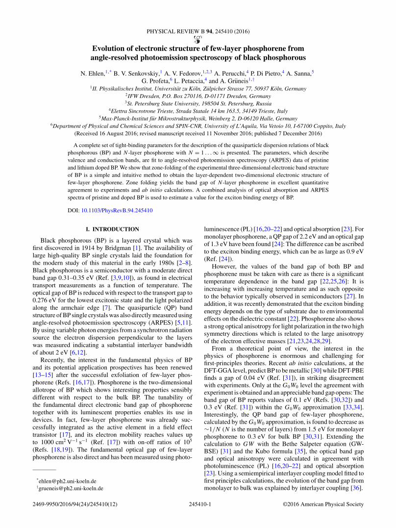
FIG. 6. Theoretical G0W0 calculations for the band structure ofBP shown in broken blue lines; our TB fit is shown in red. The paththrough the BZ is the same as for Fig. 5(a).
also because high doping levels cause a nonrigid band shift[49].
The set of TB parameters used in the calculation of theband structure reported in Fig. 5 is summarized in Table II.We find that we need to include at least six nearest in-planeneighbors to get a satisfactory fit result. Using a larger numberof parameters leads to a smoother decrease of the absolutenumber of each hopping parameter but does not improve thefit result. Thus, Table II represents an efficient interpolationscheme with a minimum number of parameters.
We also compared the TB band structure with the state-of-the-art ab initio calculations. In Fig. 6 we report the G0W0
[51] calculation of the bands for bulk BP. In all the relevantregions of the BZ, the agreement between the two sets ofbands is reasonably good. In particular the �-Z dispersionof the ARPES fit and in the G0W0 calculation has the samefeatures. This indicates that the TB fit of the ARPES data iswell suited for the zone-folding approach that we will presentin Sec. VI.
IV. TEMPERATURE DEPENDENCE OF THE OPTICALGAP AND EXCITON BINDING ENERGY
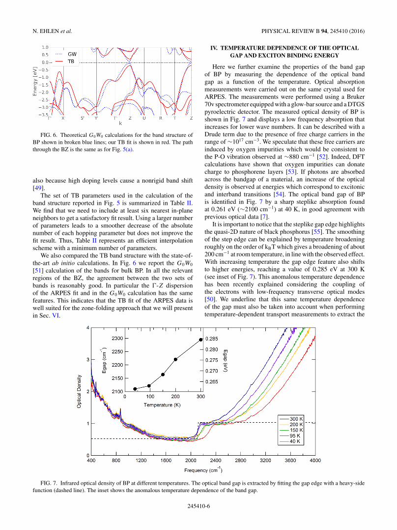
Here we further examine the properties of the band gapof BP by measuring the dependence of the optical bandgap as a function of the temperature. Optical absorptionmeasurements were carried out on the same crystal used forARPES. The measurements were performed using a Bruker70v spectrometer equipped with a glow-bar source and a DTGSpyroelectric detector. The measured optical density of BP isshown in Fig. 7 and displays a low frequency absorption thatincreases for lower wave numbers. It can be described with aDrude term due to the presence of free charge carriers in therange of ∼1017 cm−3. We speculate that these free carriers areinduced by oxygen impurities which would be consistent tothe P-O vibration observed at ∼880 cm−1 [52]. Indeed, DFTcalculations have shown that oxygen impurities can donatecharge to phosphorene layers [53]. If photons are absorbedacross the bandgap of a material, an increase of the opticaldensity is observed at energies which correspond to excitonicand interband transitions [54]. The optical band gap of BPis identified in Fig. 7 by a sharp steplike absorption foundat 0.261 eV (∼2100 cm−1) at 40 K, in good agreement withprevious optical data [7].
It is important to notice that the steplike gap edge highlightsthe quasi-2D nature of black phosphorus [55]. The smoothingof the step edge can be explained by temperature broadeningroughly on the order of kBT which gives a broadening of about200 cm−1 at room temperature, in line with the observed effect.With increasing temperature the gap edge feature also shiftsto higher energies, reaching a value of 0.285 eV at 300 K(see inset of Fig. 7). This anomalous temperature dependencehas been recently explained considering the coupling ofthe electrons with low-frequency transverse optical modes[50]. We underline that this same temperature dependenceof the gap must also be taken into account when performingtemperature-dependent transport measurements to extract the
FIG. 7. Infrared optical density of BP at different temperatures. The optical band gap is extracted by fitting the gap edge with a heavy-sidefunction (dashed line). The inset shows the anomalous temperature dependence of the band gap.
245410-6

EVOLUTION OF ELECTRONIC STRUCTURE OF FEW- . . . PHYSICAL REVIEW B 94, 245410 (2016)
value of the gap [25]. On top of the temperature dependence,the formation of excitons also affects the optical gap. If theoptical gap Egap,optical is purely excitonic, we can estimate theexcitonic binding energy by subtracting the optical band gapat T = 40 K from the ARPES band gap:
Eexc = Egap,ARPES − Egap,optical ≈ 140 meV. (8)
We note, that alternatively to the current approach, there arealso purely optical methods for determining the exciton bind-ing energy [54]. These quasiparticle spectroscopy techniquesare based on two photon photoabsorption and perform excitonspectroscopy using terahertz light [54].
V. DOPING DEPENDENCE OF THE FERMI SURFACE
In this section, we examine, using our TB model, thedoping dependence of the Fermi surface of BP. The dopingdependence of the Fermi surface is relevant for electrostaticallygated BP and the description of alkali metal doped BP. Thelatter has been predicted to become superconducting withexperimentally achievable doping levels [32]. The pairingmechanism is thought to be electron-phonon coupling, and thetopology of the Fermi surface and the total density of states atthe Fermi level have palpable impact on the coupling strength.In particular, the nesting properties of the Fermi surface canlead to instabilities in the electronic system affecting the latticedynamics and hence TC . From an experimental point of view,higher doping with respect to the one used in this work may beachieved by liquid ion gating [10] or doping by Ca atoms [56].
Weakly doped BP has only one valley around the Z point.However, a close look to the band structures of Fig. 5 andFig. 6 shows that with higher doping a second valley ofthe conduction band becomes occupied. The appearance ofmultiple Fermi surfaces is positive for superconductivity sinceit would allow us to obtain coupling from a larger set ofphonons not only low q-vector optical phonons (intrabandscattering) but also high q-vector optical and acoustic phonons
FIG. 8. The Fermi surface of BP in the BCO BZ for doping levelsof 50 meV (a), 100 meV (b), 300 meV (c), and 500 meV (d). Theappearance of a second pocket is highlighted (see text for discussion).
(mostly via interband scattering). This second valley is locatedalong the Y ’�’ direction in Fig. 5. After further doping, shiftingthe Fermi level of about 0.8 eV with respect to the pristinecase, a second conduction subband in the Z point will beoccupied. Notably, these predictions come from the TB fit todoped BP but are in excellent agreement to the ab initio G0W0
calculations that we showed above in Fig. 6.Figure 8 depicts the 3D Fermi surface as it evolves as a
function of the doping level (indicated in terms of shifts of theFermi energy 50 meV, 100 meV, 300 meV, and 500 meV) andcalculated by the TB approximation. Figure 8(d) shows thatat 500 meV electron doping a second electron pocket at the Z
point is occupied.
VI. FEW LAYER PHOSPHORENE
A. Zone-folding method
In this section, we apply the zone-folding method to thethree-dimensional electronic structure of BP in order to extractthe two-dimensional electronic dispersion relations of N -layerphosphorene. This is of high relevance as the synthesis offew-layer phosphorene in large areas that are needed forARPES is not feasible up to now. Thus for exploration ofthe electronic structure of few layer phosphorene, a simpletheoretical model is needed. Zone folding is performed inthe eight-atom cell depicted in Fig. 2(b) with the electronwave vector kz perpendicular to the phosphorene layers. Inthis description the periodicity in the kz direction is halveddue to the doubling of the unit cell along the z direction. Thisfolds back the direct band gap from the Z point of the BCOunit cell to the � point of the supercell. Modelling the N -layerphosphorene (with the layers located at zi = id,i = 1 . . . N ,with d being the interlayer distance) as infinite potentialbarriers [located at z = 0 and z = (N + 1)d] we describe theslab as an infinite potential well in the z direction, see Fig. 9.Thus, for N -layer phosphorene the electron wave functionat the zeroth and the (N + 1)th layer must be equal to zerowhich leads to the following quantization condition for itswavelength λ:
nλ = (N + 1)d, (9)
FIG. 9. Schematic representation of the zone-folding method.The orthogonal direction can be thought of as a particle-in-a-boxmodel. This leads to a quantization of the kz states.
245410-7

N. EHLEN et al. PHYSICAL REVIEW B 94, 245410 (2016)
FIG. 10. The application of the zone-folding method to BP. Performing cuts at selected kz,n as given in Eq. (10) yields a set of 2D dispersionrelations for N layer phosphorene. Here we show the dispersion along �Z of bulk BP. Cuts perpendicular to �Z correspond to the dispersionrelation of N layer phosphorene in the �Y direction. Plots for N = 1 . . . 6 layered phosphorene are shown. The cuts through the BZ of BP aredone increasingly close to the � point resulting in the reduction of the band gap for higher N .
with n being an integer. Depending on whether N is even orodd, we obtain quantization conditions for kz:
kz,n = nπ
(N + 1)d(10)
n = 1,2,3, . . . ,N/2 for N even
n = 1,2,3, . . . ,(N + 1)/2 for N odd. (11)
Thus, knowing the experimental band structure of BP, wecan describe the electronic structure of N -layer phosphoreneby cuts through the Brillouin zone of bulk BP at the kz valuesallowed by the quantization condition. Figure 10 shows aseries of plots highlighting the procedure for N = 1 . . . 6.For N layer phosphorene we obtain (N + 1)/2 (for N odd)or N/2 (for N even) kz planes in the 3D band dispersionof BP. The value(s) of kz determine the dispersion relationof N layer phosphorene in the kx-ky plane. It can be seenthat for monolayer phosphorene, the cut goes through theZ high-symmetry point of the BZ which has the highestseparation between valence and conduction bands (in thepresently used eight-atom cell). As a consequence, the gapfor monolayer phosphorene will be highest when compared toany other layer number N . For bilayer phosphorene, the kz islocated closer to the � point, and as a consequence the gapis reduced. This trend holds as we increase N and the gap israpidly approaching the bulk value since the kz move closertowards the � point according to Eq. (10).
B. Fermi surfaces of N layer phosphorene
In the remainder of this section we employ the zone-foldingmethod to calculate the electronic properties of few-layerphosphorene. We start with the layer dependence of theFermi surfaces of doped few-layer phosphorene which canbe obtained by zone folding the Fermi surface of BP in theeight-atom supercell. Figure 11(a) shows this Fermi surface ata doping level of 500 meV. It can be seen that, in the planespanned by ZU and ZT , the Fermi surface does not coverthe volume around the �Z axis. However, as kz decreases, thevolume around the �Z axis becomes occupied. This can bemore clearly seen in Fig. 11(b) which displays the contours ofthe Fermi surface from Fig. 11(a) at kz = 0. This kz dependenceis important for understanding the layer dependent Fermisurface in N layer phosphorene. Figures 11(c)–11(f) depictthe Fermi surfaces of N = 1 . . . 4 layer phosphorene. A rigidband shift of 500 meV was applied to the zone-folded bandstructure. It can be seen that the Fermi surface for N = 1consists of pockets in the �Y direction. For N � 2, anotherpocket around the � point appears. Such a layer dependencecan affect nesting and might lead to layer number dependencein the superconducting properties, similarly to what is expectedfor few-layer graphene [57].
C. Energy band gaps of N layer phosphorene
We now look in more detail to the valence and conductionband energies of N layer phosphorene and their dependence
245410-8

EVOLUTION OF ELECTRONIC STRUCTURE OF FEW- . . . PHYSICAL REVIEW B 94, 245410 (2016)
FIG. 11. (a) The Fermi surface of doped BP in the eight-atomsupercell for a doping level of 500 meV. (b) Cut through the � planeof (a). (c)–(f) The Fermi surfaces for doped 1–4 layer phosphorene.A doping level of 500 meV has been assumed here, too.
on N . To that end we plot the energies obtained from zonefolding as a function of N in Fig. 12.
It can be seen that a family pattern emerges which connectsthe nth valence (conduction) band energies for different N .
FIG. 12. Energy eigenvalues at the � point obtained from zonefolding as a function of layer number N . The blue lines connectthe energy eigenvalues of the lowest lying conduction band and theuppermost valence band. A 1/N law that governs the evolution ofeigenvalues and a family pattern can be seen.
FIG. 13. The QP and optical band gaps of few-layer phosphoreneobtained from zone folding the electronic structure of BP are denotedby •. The gap increases when going from bulk BP to monolayerphosphorene. The fit to these data according to Eq. (12) is shown by asolid red line. For comparison we show this work’s results along withpreviously published theoretical and experimental data of N -layerphosphorene: �: PL (photoluminescence) data from Ref. [20], �: PLdata from Ref. [21], �: PL data from Ref. [16], : QP calculation fromRef. [31], �: transport measurements from Ref. [59]. The turquoiseline shows the development for the four-band tight-binding modeland parameters given in Ref. [60].
Notably, similar family patterns have also been observed forfew-layer graphene [37,58] where the relevant part of thezone-folded band structure is located along the KH line ofthe hexagonal BZ. The maximum splitting between the twovalence (conduction) bands of graphite is at kz = 0 (K point)whereas at the edge of the BZ (H point) the two valence(conduction) bands are degenerate.
Calculating the difference between the lowest conductionband and the highest valence band, which is equal to the QPgap, we compare the QP gap value of N -layer phosphorene(derived from a fit to ARPES data of doped BP) with theexperimental optical and transport band gap of N layerphosphorene of previously published works and theoreticalcalculations. This comparison is shown in Fig. 13. It can beseen that the values of the gap that we obtained from zonefolding the band structure of doped BP are in excellent agree-ment to G0W0 calculations of few-layer phosphorene [31]. Theoptical band gaps of few-layer phosphorene as measured byphotoluminescence are smaller when compared to the QP bandgaps. Despite some scattering in the experimental data, wecan observe an increase of the difference between QP gap andoptical band gap with decreasing the number of layers. Again,we infer that this trend can be understood as excitonic effectsbecoming increasingly important for thinner systems. On theother hand, the large variation among individual experimentscould perhaps be explained by (1) different environmentswhich have a large effect on the exciton binding energy and(2) different degrees of oxygen exposure which causes dopingand hence a change in the optical response.
The dependence of the gap Eg(N ) on the layer number N
can be fitted by
Eg(N ) = 1.99e−0.18x
N0.52+ 0.41. (12)
245410-9

N. EHLEN et al. PHYSICAL REVIEW B 94, 245410 (2016)
FIG. 14. Evolution of the band gap as a function of layer numberN is inversely proportional to the number of layers [see Eq. (12)].The dots show the actual gaps for given values of 1/N ; the red lineshows an interpolated spline between these values.
This mix of shallow exponential decay and N−a dependenceis similar to previous results for a four-band tight-bindingHamiltonian that was fit to GW0 calculations [60]. In order tocover a wider range of N we also show the plot of the bandgap as a function of 1/N in Fig. 14.
Finally, since zone folding does not capture effects resultingfrom crystal surfaces, it is interesting to assess the accuracy ofzone folding by a comparison of the zone-folded band structureto an explicit TB calculation of N layer phosphorene. The cal-culation of N layer phosphorene uses an extended Hamiltonianwhich includes the coupling to adjacent phosphorene layers viathe out-of-plane matrix elements. The atoms inside the layerson the two surfaces of the few-layer phosphorene stack willhave fewer neighbors to couple to in the extended calculation.This effect is not included in the zone-folding picture whichderives the bands of few-layer phosphorene from the BP.The comparison of the zone-folding result and the extended
FIG. 15. Comparison of the band structure for N = 7 layerphosphorene obtained by (a) zonefolding and (b) an explicit tight-binding calculation using an extended Hamiltonian.
calculation is shown in Fig. 15. Since black phosphorus is avan der Waals material without dangling bonds, the effects ofsurfaces are believed to be small, and indeed it can be seen thatthe zone-folding result agrees well with the explicit calculationof N layer phosphorene.
VII. DISCUSSION AND OUTLOOK
ARPES measurements of the three-dimensional electronicstructure of BP allowed us to perform a fit of tight-bindingparameters of black phosphorus using the Slater-Koster ap-proximation. The experimental data could be described usingfive in-plane and two out-of-plane neighbor orders. Usingthis model with our parameters we extract the behavior forthe band gap of N -layer phosphorene from the bulk bandsusing the zone-folding method and find good agreement withcalculations and experiments.
Measurements of the optical energy gap indicate that thegap value is close to this separation energy. Moreover thevalence band effective mass is not affected by doping in ourcase, and ab initio G0W0 calculations are in agreement withthe measured conduction band. From these facts we inferthat our doping levels by lithium cause little structural andelectronic changes apart from the rigid band shift. The ARPESdata of pristine and doped BP are therefore used to fit anew set of tight-binding parameters to the experiment. Thisaccurate set of tight-binding parameters is used to predict atransition into a multiple-valley ground state upon alkali metaldoping of BP. Already at experimentally accessible dopinglevels it is possible to obtain a large Fermi surface area andtherefore to take advantage of the full phononic coupling,without relevant momentum restrictions. Most importantly,we employ the zone-folding method to predict the electronenergy gap of few-layer phosphorene. The predicted valuesshow the same trend as the experimentally observed energyband gaps of few-layer phosphorene. Finally, the experimentalband structure data are compared to ab initio calculations usingthe G0W0 approximation, and a good agreement is found inmost parts of the Brillouin zone. The present work is basedon lithium doped BP in the regime of a rigid band shift. Itwould be interesting to extend it to other alkali or alkalineearth dopants for which effects beyond a rigid band shift couldbe observed. The proposed tight-binding model can also beuseful to describe the electronic structure of gated few-layerphosphorene devices. This would require modifying the on-sitetight-binding parameters in a calculation using an extendedHamiltonian of few-layer phosphorene in such a way to modela different charge on each layer.
ACKNOWLEDGMENTS
N.E., B.S., and A.G. acknowledge the ERC GrantNo. 648589 ‘SUPER-2D’ and support by DFG throughCRC1238 project A1. B.S. and A.G. acknowledge theDFG project GR 3708/2-1. The stay at the Elet-tra synchrotron for ARPES and optical absorption ex-periments has been supported by the CERIC-ERICconsortium.
245410-10
EVOLUTION OF ELECTRONIC STRUCTURE OF FEW- . . . PHYSICAL REVIEW B 94, 245410 (2016)
[1] P. W. Bridgman, J. Am. Chem. Soc. 36, 1344 (1914).[2] Y. Takao, H. Asahina, and A. Morita, J. Phys. Soc. Jpn. 50, 3362
(1981).[3] Y. Maruyama, S. Suzuki, K. Kobayashi, and S. Tanuma, Physica
B+C 105, 99 (1981).[4] S.-i. Narita, S.-i. Terada, S. Mori, K. Muro, Y. Akahama, and
S. Endo, J. Phys. Soc. Jpn. 52, 3544 (1983).[5] T. Takahashi, H. Tokailin, S. Suzuki, T. Sagawa, and I. Shirotani,
Phys. Rev. B 29, 1105 (1984).[6] T. Takahashi, N. Gunasekara, H. Ohsawa, H. Ishii, T. Kinoshita,
S. Suzuki, T. Sagawa, H. Kato, T. Miyahara, and I. Shirotani,Phys. Rev. B 33, 4324 (1986).
[7] A. Morita, Appl. Phys. A 39, 227 (1986).[8] S. Endo, Y. Akahama, S.-i. Terada, and S.-i. Narita, Jpn. J. Appl.
Phys. 21, L482 (1982).[9] R. W. Keyes, Phys. Rev. 92, 580 (1953).
[10] Y. Saito and Y. Iwasa, ACS Nano 9, 3192 (2015).[11] T. Takahashi, H. Tokailin, S. Suzuki, T. Sagawa, and I. Shirotani,
J. Phys. C 18, 825 (1985).[12] L. Liang, J. Wang, W. Lin, B. G. Sumpter, V. Meunier, and
M. Pan, Nano Lett. 14, 6400 (2014).[13] X. Ling, H. Wang, S. Huang, F. Xia, and M. S. Dresselhaus,
Proc. Natl. Acad. Sci. USA 112, 4523 (2015).[14] H. Liu, Y. Du, Y. Deng, and P. D. Ye, Chem. Soc. Rev. 44, 2732
(2015).[15] J. Ribeiro-Soares, R. M. Almeida, L. G. Cancado, M. S.
Dresselhaus, and A. Jorio, Phys. Rev. B 91, 205421 (2015).[16] H. Liu, A. T. Neal, Z. Zhu, Z. Luo, X. Xu, D. Tomanek, and
P. D. Ye, ACS Nano 8, 4033 (2014).[17] L. Li, Y. Yu, G. J. Ye, Q. Ge, X. Ou, H. Wu, D. Feng, X. H.
Chen, and Y. Zhang, Nat. Nanotechnol. 9, 372 (2014).[18] S. P. Koenig, R. A. Doganov, H. Schmidt, A. H. Castro Neto,
and B. Ozyilmaz, Appl. Phys. Lett. 104, 103106 (2014).[19] V. Tayari, N. Hemsworth, I. Fakih, A. Favron, E. Gaufres, G.
Gervais, R. Martel, and T. Szkopek, Nat. Commun. 6, 7702(2015).
[20] J. Yang, R. Xu, J. Pei, Y. W. Myint, F. Wang, Z. Wang, S. Zhang,Z. Yu, and Y. Lu, Light. Sci. Appl. 4, e312 (2015).
[21] S. Zhang, J. Yang, R. Xu, F. Wang, W. Li, M. Ghufran, Y.-W.Zhang, Z. Yu, G. Zhang, Q. Qin, and Y. Lu, ACS Nano 8, 9590(2014).
[22] A. Surrente, A. A. Mitioglu, K. Galkowski, W. Tabis, D. K.Maude, and P. Plochocka, Phys. Rev. B 93, 121405 (2016).
[23] L. Li, J. Kim, C. Jin, G. Ye, D. Y. Qiu, F. H. da Jornada, Z. Shi,L. Chen, Z. Zhang, F. Yang, K. Watanabe, T. Taniguchi, W. Ren,S. G. Louie, X. Chen, Y. Zhang, and F. Wang, Nat. Nanotech.(2016), doi:10.1038/nnano.2016.171.
[24] X. Wang, A. M. Jones, K. L. Seyler, V. Tran, Y. Jia, H. Zhao, H.Wang, L. Yang, X. Xu, and F. Xia, Nat. Nano 10, 517 (2015).
[25] D. Warschauer, J. Appl. Phys. 34, 1853 (1963).[26] M. Baba, Y. Nakamura, K. Shibata, and A. Morita, Jpn. J. Appl.
Phys. 30, L1178 (1991).[27] E. Burstein, Phys. Rev. 93, 632 (1954).[28] R. Schuster, J. Trinckauf, C. Habenicht, M. Knupfer, and B.
Buchner, Phys. Rev. Lett. 115, 026404 (2015).[29] X. Ling, S. Huang, E. H. Hasdeo, L. Liang, W. M. Parkin, Y.
Tatsumi, A. R. T. Nugraha, A. A. Puretzky, P. M. Das, B. G.Sumpter, D. B. Geohegan, J. Kong, R. Saito, M. Drndic, V.Meunier, and M. S. Dresselhaus, Nano Lett. 16, 2260 (2016).
[30] A. N. Rudenko and M. I. Katsnelson, Phys. Rev. B 89, 201408(2014).
[31] V. Tran, R. Soklaski, Y. Liang, and L. Yang, Phys. Rev. B 89,235319 (2014).
[32] A. Sanna, A. V. Fedorov, N. I. Verbitskiy, J. Fink, C. Krellner, L.Petaccia, A. Chikina, D. Y. Usachov, A. Gruneis, and G. Profeta,2D Materials 3, 025031 (2016).
[33] L. Hedin, Phys. Rev. 139, A796 (1965).[34] M. S. Hybertsen and S. G. Louie, Phys. Rev. B 34, 5390 (1986).[35] T. Low, A. S. Rodin, A. Carvalho, Y. Jiang, H. Wang, F. Xia,
and A. H. Castro Neto, Phys. Rev. B 90, 075434 (2014).[36] V. Wang, Y. C. Liu, Y. Kawazoe, and W. T. Geng, J. Phys. Chem.
Lett. 6, 4876 (2015).[37] A. Gruneis, C. Attaccalite, L. Wirtz, H. Shiozawa, R. Saito, T.
Pichler, and A. Rubio, Phys. Rev. B 78, 205425 (2008).[38] X.-L. Qi and S.-C. Zhang, Rev. Mod. Phys. 83, 1057 (2011).[39] E. Cappelluti and G. Profeta, Phys. Rev. B 85, 205436
(2012).[40] S. Fukuoka, T. Taen, and T. Osada, J. Phys. Soc. Jpn. 84, 121004
(2015).[41] J. L. Lado and J. Fernandez-Rossier, 2D Mater. 3, 035023
(2016).[42] A. Brown and S. Rundqvist, Acta Crystallogr. 19, 684
(1965).[43] J. C. Slater and G. F. Koster, Phys. Rev. 94, 1498 (1954).[44] L. Petaccia, P. Vilmercati, S. Gorovikov, M. Barnaba, A. Bianco,
D. Cocco, C. Masciovecchio, and A. Goldoni, Nucl. Instrum.Methods Phys. Res., Sect. A: Accelerators, Spectrometers,Detectors and Associated Equipment 606, 780 (2009).
[45] A. Damascelli, Phys. Scr. T109, 61 (2004).[46] C. Q. Han, M. Y. Yao, X. X. Bai, L. Miao, F. Zhu, D. D. Guan,
S. Wang, C. L. Gao, C. Liu, D. Qian, and et al., Phys. Rev. B90, 085101 (2014).
[47] E. Golias, M. Krivenkov, and J. Sanchez-Barriga, Phys. Rev. B93, 075207 (2016).
[48] A. Fedorov, C. S. Praveen, N. I. Verbitskiy, D. Haberer, D.Usachov, D. V. Vyalikh, A. Nefedov, C. Woll, L. Petaccia, S.Piccinin, H. Sachdev, M. Knupfer, B. Buchner, S. Fabris, andA. Gruneis, Phys. Rev. B 92, 125440 (2015).
[49] J. Kim, S. S. Baik, S. H. Ryu, Y. Sohn, S. Park, B.-G. Park, J.Denlinger, Y. Yi, H. J. Choi, and K. S. Kim, Science 349, 723(2015).
[50] C. E. P. Villegas, A. R. Rocha, and A. Marini, Nano Lett. 16,5095 (2016).
[51] All calculations have been performed at the experimental latticewith the Vienna ab initio simulation package (VASP) [61,62]and within the generalized gradient approximation [63] (GGA)to density functional theory. We used projected augmented-wave(PAW) [64] pseudopotentials. A cutoff of 300 eV was used forthe plane-wave expansion and a 100 eV cutoff for the summationof the response function. BZ sampling has been done with a �
centered 12 × 12 × 8k-point grid.[52] J. D. Wood, S. A. Wells, D. Jariwala, K.-S. Chen, E. Cho, V. K.
Sangwan, X. Liu, L. J. Lauhon, T. J. Marks, and M. C. Hersam,Nano Lett. 14, 6964 (2014).
[53] A. Ziletti, A. Carvalho, D. K. Campbell, D. F. Coker, and A. H.Castro Neto, Phys. Rev. Lett. 114, 046801 (2015).
[54] S. W. Koch, M. Kira, G. Khitrova, and H. M. Gibbs, Nat. Mater.5, 523 (2006).
245410-11

N. EHLEN et al. PHYSICAL REVIEW B 94, 245410 (2016)
[55] M. Dressel and G. Gruner, Electrodynamics of Solids: OpticalProperties of Electrons in Matter (Cambridge University Press,2002).
[56] A. V. Fedorov, N. I. Verbitskiy, D. Haberer, C. Struzzi, L.Petaccia, D. Usachov, O. Y. Vilkov, D. V. Vyalikh, J. Fink, M.Knupfer, B. Buchner, and A. Gruneis, Nat. Commun. 5, 4257(2014).
[57] E. R. Margine, H. Lambert, and F. Giustino, Sci. Rep. 6, 21414(2016).
[58] K. F. Mak, M. Y. Sfeir, J. A. Misewich, and T. F. Heinz, Proc.Natl. Acad. Sci. USA 107, 14999 (2010).
[59] X. Chen, L. Wang, Y. Wu, H. Gao, Y. Wu, G. Qin, Z. Wu, Y.Han, S. Xu, T. Han, W. Ye, J. Lin, G. Long, Y. He, Y. Cai, W.Ren, and N. Wang, 2D Mater. 3, 015012 (2016).
[60] A. N. Rudenko, S. Yuan, and M. I. Katsnelson, Phys. Rev. B 92,085419 (2015).
[61] G. Kresse and J. Furthmuller, Phys. Rev. B 54, 11169 (1996).[62] G. Kresse and J. Furthmuller, Comput. Mater. Sci. 6, 15
(1996).[63] J. P. Perdew, K. Burke, and M. Ernzerhof, Phys. Rev. Lett. 77,
3865 (1996).[64] P. E. Blochl, Phys. Rev. B 50, 17953 (1994).
245410-12
Related Documents