Edited by Semiconductor Infrared Devices and Applications A. G. Unil Perera Printed Edition of the Special Issue Published in Micromachines www.mdpi.com/journal/micromachines

Welcome message from author
This document is posted to help you gain knowledge. Please leave a comment to let me know what you think about it! Share it to your friends and learn new things together.
Transcript

Edited by
Semiconductor Infrared Devices and Applications
A. G. Unil Perera
Printed Edition of the Special Issue Published in Micromachines
www.mdpi.com/journal/micromachines

Semiconductor Infrared Devices andApplications

Semiconductor Infrared Devices andApplications
Editor
A. G. Unil Perera
MDPI • Basel • Beijing • Wuhan • Barcelona • Belgrade • Manchester • Tokyo • Cluj • Tianjin
Editor
A. G. Unil Perera
Georgia State University
USA
Editorial Office
MDPI
St. Alban-Anlage 66
4052 Basel, Switzerland
This is a reprint of articles from the Special Issue published online in the open access journal
Micromachines (ISSN 2072-666X) (available at: https://www.mdpi.com/journal/micromachines/
special issues/Semiconductor Infrared Devices).
For citation purposes, cite each article independently as indicated on the article page online and as
indicated below:
LastName, A.A.; LastName, B.B.; LastName, C.C. Article Title. Journal Name Year, Volume Number,
Page Range.
ISBN 978-3-0365-3353-7 (Hbk)
ISBN 978-3-0365-3354-4 (PDF)
© 2022 by the authors. Articles in this book are Open Access and distributed under the Creative
Commons Attribution (CC BY) license, which allows users to download, copy and build upon
published articles, as long as the author and publisher are properly credited, which ensures maximum
dissemination and a wider impact of our publications.
The book as a whole is distributed by MDPI under the terms and conditions of the Creative Commons
license CC BY-NC-ND.
Contents
About the Editor . . . . . . . . . . . . . . . . . . . . . . . . . . . . . . . . . . . . . . . . . . . . . . vii
A. G. Unil Perera
Editorial for the Special Issue on Semiconductor Infrared Devices and ApplicationsReprinted from: Micromachines 2021, 12, 1069, doi:10.3390/mi12091069 . . . . . . . . . . . . . . . 1
Raphael Muller, Marko Haertelt, Jasmin Niemasz, Klaus Schwarz, Volker Daumer, Yuri V.
Flores, Ralf Ostendorf and Robert Rehm
Thermoelectrically-Cooled InAs/GaSb Type-II Superlattice Detectors as an Alternative toHgCdTe in a Real-Time Mid-Infrared Backscattering Spectroscopy SystemReprinted from: Micromachines 2020, 11, 1124, doi:10.3390/mi11121124 . . . . . . . . . . . . . . . 5
Ru Chen, Zhiqing Lu and Kun Zhao
Manganite Heterojunction Photodetector with Broad Spectral Response Range from 200 nm to2 μmReprinted from: Micromachines 2020, 11, 129, doi:10.3390/mi11020129 . . . . . . . . . . . . . . . . 19
Gamini Ariyawansa, Joshua Duran, Charles Reyner and John Scheihing
InAs/InAsSb Strained-Layer Superlattice Mid-Wavelength Infrared Detector forHigh-Temperature OperationReprinted from: Micromachines 2019, 10, 806, doi:10.3390/mi10120806 . . . . . . . . . . . . . . . 25
Hasan Goktas and Fikri Serdar Gokhan
Analysis and Simulation of Forcing the Limits of Thermal Sensing for Microbolometers inCMOS–MEMS TechnologyReprinted from: Micromachines 2019, 10, 733, doi:10.3390/mi10110733 . . . . . . . . . . . . . . . . 33
David Z. Ting, Sir B. Rafol, Arezou Khoshakhlagh, Alexander Soibel, Sam A. Keo, Anita M.
Fisher, Brian J. Pepper, Cory J. Hill and Sarath D. Gunapala
InAs/InAsSb Type-II Strained-Layer Superlattice Infrared PhotodetectorsReprinted from: Micromachines 2020, 11, 958, doi:10.3390/mi11110958 . . . . . . . . . . . . . . . 43
Rayyan Manwar, Karl Kratkiewicz and Kamran Avanaki
Overview of Ultrasound Detection Technologies for Photoacoustic ImagingReprinted from: Micromachines 2020, 11, 692, doi:10.3390/mi11070692 . . . . . . . . . . . . . . . . 61
Hemendra Ghimire, P. V. V. Jayaweera, Divya Somvanshi, Yanfeng Lao and A. G. Unil Perera
Recent Progress on Extended Wavelength and Split-Off Band HeterostructureInfrared DetectorsReprinted from: Micromachines 2020, 11, 547, doi:10.3390/mi11060547 . . . . . . . . . . . . . . . . 85
v

About the Editor
A. G. Unil Perera received a B.S. degree in physics (with first class honors) from the University
of Colombo, Sri Lanka, and M.S. and Ph.D. degrees from the University of Pittsburgh. He is currently
a Regents’ Professor at the Department of Physics and Astronomy, Georgia State University, Atlanta.
He is a Fellow of the IEEE and Life Fellow of both SPIE and APS. His research focus is on developing
tunable and bias selectable detectors responding from UV to FIR and IR applications in disease
detection. He has 11 patents, 4 edited books, 11 invited book chapters, and over 200 publications. He
has received various awards from the Outstanding Junior Faculty Award and Outstanding Faculty
Achievement Award to the Alumni Distinguished Professor Award at GSU. He is also a member of
the editorial board for the IEEE Journal of Electron Device Society and also an IEEE Photonics Society
Distinguished Lecturer for 2020–2022.
vii

micromachines
Editorial
Editorial for the Special Issue on Semiconductor InfraredDevices and Applications
A. G. Unil Perera
Citation: Perera, A.G.U. Editorial for
the Special Issue on Semiconductor
Infrared Devices and Applications.
Micromachines 2021, 12, 1069. https://
doi.org/10.3390/mi12091069
Received: 23 August 2021
Accepted: 26 August 2021
Published: 2 September 2021
Publisher’s Note: MDPI stays neutral
with regard to jurisdictional claims in
published maps and institutional affil-
iations.
Copyright: © 2021 by the author.
Licensee MDPI, Basel, Switzerland.
This article is an open access article
distributed under the terms and
conditions of the Creative Commons
Attribution (CC BY) license (https://
creativecommons.org/licenses/by/
4.0/).
Department of Physics & Astronomy, Georgia State University, Atlanta, GA 30303, USA;[email protected]
Infrared radiation (IR) was accidentally discovered in 1800 by the astronomer SirWilliam Herschel. While trying to study the visible light spectrum and energy in eachcomponent, he discovered a type of invisible radiation in the spectrum that was lowerin energy than red light. The thermometer used in his experiment can be considered thevery first infrared detector, which is categorized as a thermal detector. The first intentionalinfrared detector is the thermopile developed by Macedonio Melloni in 1835 [1]. One of theearly semiconductor materials used as an infrared device was lead sulfide (PbS) [2]. Afterthe second World War, the interest in infrared devices dramatically increased as it becameclear that infrared could be used to obtain images of objects due to their heat emission.A detailed history of infrared detector development is presented by Anthony Roglaskiin a review article [3]. This led to the establishment of dedicated research facilities fordeveloping infrared detectors such as the Royal Radar Establishment in Malvern, now theQinetic in the UK, and the US Army Night Vision Laboratory, now the Night Vision andElectronic Sensors Directorate (NVESD) in VA. This focus on infrared imaging for defenseapplications fueled the rapid development of the field especially for the three atmosphericwindows of short-wave IR (SWIR 0.7–2 μm), mid-wave IR (MWIR 3–5 μm), and long-waveIR (LWIR 8–14 μm), where the atmosphere is relatively transparent. The room temperature(300 K) black body radiation happens to peak at 10 μm, which is in the LWIR range.
For a long time, the most studied infrared detector material was HgCdTe, whichwas heavily used in military applications for night vision, remote sensing, and infraredastronomy research. Changing the Cd composition allowed for the detector to cover the fullwavelength spectrum, covering all three ranges from SWIR and MWIR to LWIR. However,the operating temperature of 77 K was a concern for cost-conscious applications. Morerecently, after the development of novel thin film growth techniques such as molecularbeam epitaxy (MBE) and metal–organic chemical vapor deposition (MOCVD), other mate-rials were studied as possible infrared detectors. These developments led to the fast-paceddevelopment of the quantum well [4,5], the quantum dot [6,7], and Type II superlattice [8,9]detectors covering various material systems and multiple wavelength ranges. Most of thesetypes of detectors were specifically geared towards various wavelength ranges and specificmaterial systems were developed for each type of detector. Other detection principalsbased on physics were also studied [10,11], covering a wider wavelength range and withthe possibility of being used with any material, which will be advantageous for materialsthat are already developed. More recently, the idea of extending the accepted standardwavelength threshold governed by the equation λt =
1.24Δ was demonstrated [12]. Here, λt
is the threshold wavelength limit in μms and Δ is the energy gap in meV. All the above-mentioned detector types are known as photon detectors, which are generally much fasterthan the detectors categorized as thermal detectors. However, thermal detectors [13] havea broad spectral range and cost advantage, making them useful for most practical applica-tions for which millisecond response times are acceptable. Bolometers [14], which belongto the thermal detectors, have also undergone further development due to the adventof microbolometers. Recent technological advances allowing for microstructure designs
Micromachines 2021, 12, 1069. https://doi.org/10.3390/mi12091069 https://www.mdpi.com/journal/micromachines
1
Micromachines 2021, 12, 1069
have improved the response time of novel microbolometers, providing cost-effective andreasonably fast infrared detectors for mass production applications. The strong opticalabsorption in human tissue can, in general, be a limitation for optical imaging used formedical diagnosis. This absorbed energy leads to the thermal expansion of tissue, whichcan generate ultrasound energy when detected by a transducer and produce images ofoptical absorption contrast within tissues, now known as photoacoustic imaging [15]. Awide variety of infrared detectors have provided application opportunities for almost allareas of humanity involving security and defense, biomedical, commercial, industrial, andscientific research. In fact, the very first technique for checking COVID-19 used a near IRthermometer, which can detect body temperature without contact, providing a safe, quick,and easy way to measure the body temperature.
This Special Issue has seven papers covering various aspects of photon detectiontechniques. Three papers (the first, third, and fifth in this Special Issue) focus on Type IIsuperlattice (SL) infrared detectors. In antimonide-based III–V materials grown on theGaSb substrate, the epi layers (grown on the GaSb substrate) can be lattice-matched orstrained. For example, one can grow a thick layer of bulk InAs0.91Sb0.09 alloy, which islattice-matched to GaSb with no strain in the layer. Similarly, an InAs0.91Sb0.09/GaSbsuperlattice also has no strain in the constituent layers as they all are lattice-matched tothe GaSb substrate. Conversely, one can design a superlattice with two constituent layers,which are not lattice-matched but maintain the overall strain in the superlattice layer atzero. These are called ‘strained’ layer superlattices (SLS) because the individual layers arestrained (tensile or compressive). For example, in a Ga-free InAs/InAs(1-x)Sbx superlattice,the InAs layer is tensile-strained, while the InAs(1-x)Sbx layer is compressively strained.The alloy composition (x) and layer thickness are the two parameters used to balance thestrain in the superlattice unit cell. Similar to InAs/InAsSb superlattices, InAs/InGaSb su-perlattices are also strained. All the Sb-based superlattices are not technically strained (e.g.,InAs0.91Sb0.09/GaSb); however, all the commonly used superlattices to date are strained.The first paper in this Special Issue, by Raphael Müller et al. from the Fraunhofer In-stitute, discusses the performance comparison of an InAs/GaSb Type II SL IR detectorwith the HgCdTe detector in a real-time spectroscopic application [16]. Comparison ofroughly a decade of progress (of Type II IR detectors) with more than a half century ofprogress in HgCdTe IR detectors itself gives an indication of the rapid advances in theIII–V-material-based infrared devices. The second paper, by Ru Chen et al. of ChinaUniversity of Petroleum in Beijing, discusses a manganite-based perovskite-type oxideheterojunction showing ultraviolet-to-near-infrared photo response up to room tempera-ture [17]. Perovskite-type oxides are complex metal oxides with important applicationsas electrical, magnetic, and catalytic materials. The third and fifth papers here are basedon InAs/InAsSb SLS structures by Gamini Ariyawansa et al. from the Air Force ResearchLaboratory [18] in Dayton, Ohio, and David Ting et al. from NASA JPL. Ariyawansa et al.discusses a mid-wavelength infrared detector and a focal plane array for high-temperatureoperations, utilizing the nBn architecture in their SLS. The fifth paper from David Tinget al. from JPL provides a discussion on the emergence of the Type II SLS infrared detectorsand discusses the advantages, disadvantages, and recent developments [19]. In the lasttwo decades, IR detectors are being specifically introduced in biomedical imaging. Thefourth paper is from Hasan Göktas et al. from Harran University in Turkey and discussesthe limits of thermal sensing for microbolometers, proposing a method to improve thethermal sensitivity [20]. The sixth paper by Rayyan Manwar et al. from the University ofIllinois in Chicago discusses a novel imaging technique that combines the benefits of opticalresolution and acoustic depth of penetration, denoted as photoacoustic imaging [21]. Thelast paper of the volume, by Hemendra Ghimire et al. from the Georgia State University,discusses the concept of a heterojunction infrared detector that can be used with any semi-conductor material [22]. They also describe a possible approach to detect longer thresholdwavelengths beyond the corresponding energy thresholds, giving rise to the possibilityof higher operating temperatures for longer wavelength detectors. Overall, this volume
2
Micromachines 2021, 12, 1069
covers the well-developed fast response HgCdTe photon detectors to the more recentlydeveloped Type II SLS detectors, reasonably fast microbolometer thermal detectors, up andcoming photoacoustic detection and imaging, and concludes with a detection technique us-ing a novel intriguing idea of going beyond the very well-established energy gap thresholdwavelength rule.
Funding: This research received no external funding.
Conflicts of Interest: The author declares no conflict of interest.
References
1. Schettino, E. A new instrument for infrared radiation measurements: The thermopile of Macedonio Melloni. Ann. Sci. 1989, 46,511–517. [CrossRef]
2. Putley, E.H.; Arthur, J.B. Lead Sulphide—An Intrinsic Semiconductor. Proc. Phys. Soc. Sect. B 1951, 64, 616–618. [CrossRef]3. Rogalski, A. History of infrared detectors. Opto-Electron. Rev. 2012, 20, 279–308. [CrossRef]4. Coon, D.D.; Karunasiri, R.P.G. New mode of IR detection using quantum wells. Appl. Phys. Lett. 1984, 45, 649. [CrossRef]5. Levine, B.F. Quantum-well infrared photodetectors. J. Appl. Phys. 1993, 74, R1–R81. [CrossRef]6. Bhattacharya, P.; Mi, Z. Quantum-Dot Optoelectronic Devices. Proc. IEEE 2007, 95, 1723–1740. [CrossRef]7. Razeghi, M.; Esaki, L.; von Klitzing, K. (Eds.) The Wonder of Nanotechnology: Quantum Optoelectronic Devices and Applications; SPIE:
Bellingham, WA, USA, 2013; pp. 1–893.8. Smith, D.L.; Mailhiot, C. Proposal for strained type II superlattice infrared detectors. J. Appl. Phys. 1987, 62, 2545–2548. [CrossRef]9. Ting, D.Z.-Y.; Soibel, A.; Höglund, L.; Nguyen, J.; Hill, C.J.; Khoshakhlagh, A.; Gunapala, S.D. Type-II Superlattice Infrared
Detectors. In Semiconductors and Semimetals; Elsevier BV: Amsterdam, The Netherlands, 2011; Volume 84, pp. 1–57.10. Perera, A. Heterojunction and superlattice detectors for infrared to ultraviolet. Prog. Quantum Electron. 2016, 48, 1–56. [CrossRef]11. Szmulowicz, F.; Madarasz, F.L. Blocked impurity band detectors—An analytical model: Figures of merit. J. Appl. Phys. 1987, 62,
2533–2540. [CrossRef]12. Lao, Y.F.; Perera, A.U.; Li, L.H.; Khanna, S.P.; Linfield, E.H.; Liu, H.C. Tunable hot-carrier photodetection beyond the bandgap
spectral limit. Nat. Photonics 2014, 8, 412–418. [CrossRef]13. Talghader, J.J.; Gawarikar, A.S.; Shea, R.P. Spectral selectivity in infrared thermal detection. Light. Sci. Appl. 2012, 1, e24.
[CrossRef]14. Perera, A.G.U. (Ed.) Bolometers; IntechOpen: Rijeka, Croatia, 2012; ISBN 978-953-81-0235-09. [CrossRef]15. Beard, P. Biomedical photoacoustic imaging. Interface Focus 2011, 1, 602–631. [CrossRef] [PubMed]16. Müller, R.; Haertelt, M.; Niemasz, J.; Schwarz, K.; Daumer, V.; Flores, Y.V.; Ostendorf, R.; Rehm, R. Thermoelectrically-Cooled
InAs/GaSb Type-II Superlattice Detectors as an Alternative to HgCdTe in a Real-Time Mid-Infrared Backscattering SpectroscopySystem. Micromachines 2020, 11, 1124. [CrossRef] [PubMed]
17. Chen, R.; Lu, Z.; Zhao, K. Manganite Heterojunction Photodetector with Broad Spectral Response Range from 200 nm to 2 μm.Micromachines 2020, 11, 129. [CrossRef] [PubMed]
18. Ariyawansa, G.; Duran, J.; Reyner, C.; Scheihing, J. InAs/InAsSb Strained-Layer Superlattice Mid-Wavelength Infrared Detectorfor High-Temperature Operation. Micromachines 2019, 10, 806. [CrossRef] [PubMed]
19. Ting, D.Z.; Rafol, S.B.; Khoshakhlagh, A.; Soibel, A.; Keo, S.A.; Fisher, A.M.; Pepper, B.J.; Hill, C.J.; Gunapala, S.D. InAs/InAsSbType-II Strained-Layer Superlattice Infrared Photodetectors. Micromachines 2020, 11, 958. [CrossRef] [PubMed]
20. Göktas, H.; Gökhan, F.S. Analysis and Simulation of Forcing the Limits of Thermal Sensing for Microbolometers in CMOS–MEMSTechnology. Micromachines 2019, 10, 733. [CrossRef] [PubMed]
21. Manwar, R.; Kratkiewicz, K.; Avanaki, K. Overview of Ultrasound Detection Technologies for Photoacoustic Imaging. Microma-chines 2020, 11, 692. [CrossRef] [PubMed]
22. Ghimire, H.; Jayaweera, P.V.V.; Somvanshi, D.; Lao, Y.; Perera, A.G.U. Recent Progress on Extended Wavelength and Split-OffBand Heterostructure Infrared Detectors. Micromachines 2020, 11, 547. [CrossRef] [PubMed]
3

micromachines
Article
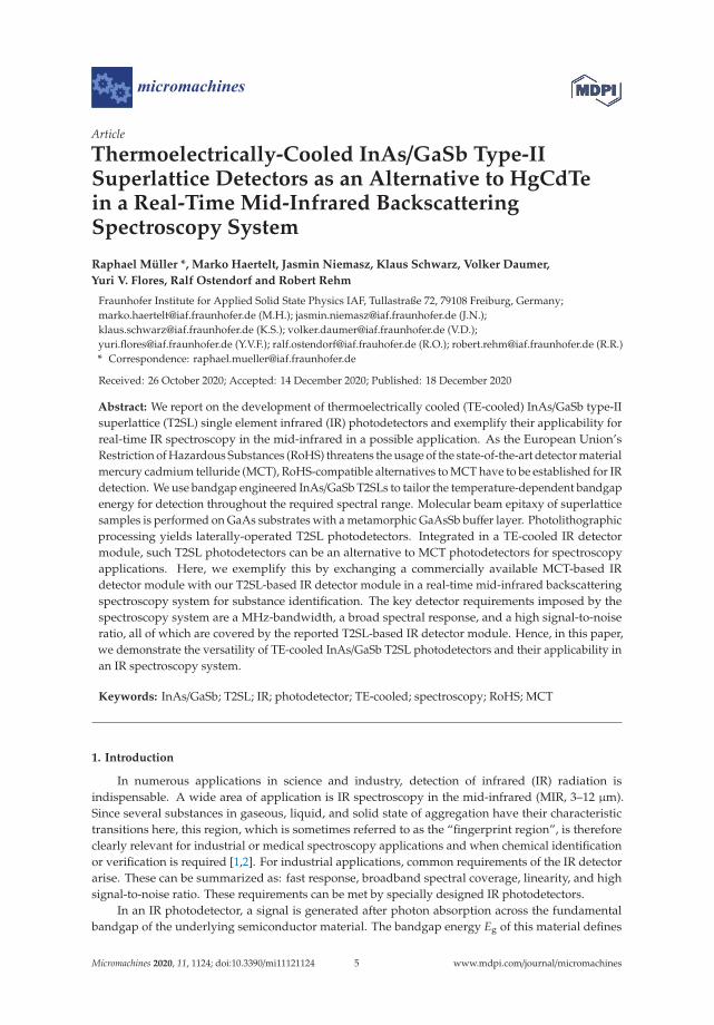
Thermoelectrically-Cooled InAs/GaSb Type-IISuperlattice Detectors as an Alternative to HgCdTein a Real-Time Mid-Infrared BackscatteringSpectroscopy System
Raphael Müller *, Marko Haertelt, Jasmin Niemasz, Klaus Schwarz, Volker Daumer,
Yuri V. Flores, Ralf Ostendorf and Robert Rehm
Fraunhofer Institute for Applied Solid State Physics IAF, Tullastraße 72, 79108 Freiburg, Germany;[email protected] (M.H.); [email protected] (J.N.);[email protected] (K.S.); [email protected] (V.D.);[email protected] (Y.V.F.); [email protected] (R.O.); [email protected] (R.R.)* Correspondence: [email protected]
Received: 26 October 2020; Accepted: 14 December 2020; Published: 18 December 2020
Abstract: We report on the development of thermoelectrically cooled (TE-cooled) InAs/GaSb type-IIsuperlattice (T2SL) single element infrared (IR) photodetectors and exemplify their applicability forreal-time IR spectroscopy in the mid-infrared in a possible application. As the European Union’sRestriction of Hazardous Substances (RoHS) threatens the usage of the state-of-the-art detector materialmercury cadmium telluride (MCT), RoHS-compatible alternatives to MCT have to be established for IRdetection. We use bandgap engineered InAs/GaSb T2SLs to tailor the temperature-dependent bandgapenergy for detection throughout the required spectral range. Molecular beam epitaxy of superlatticesamples is performed on GaAs substrates with a metamorphic GaAsSb buffer layer. Photolithographicprocessing yields laterally-operated T2SL photodetectors. Integrated in a TE-cooled IR detectormodule, such T2SL photodetectors can be an alternative to MCT photodetectors for spectroscopyapplications. Here, we exemplify this by exchanging a commercially available MCT-based IRdetector module with our T2SL-based IR detector module in a real-time mid-infrared backscatteringspectroscopy system for substance identification. The key detector requirements imposed by thespectroscopy system are a MHz-bandwidth, a broad spectral response, and a high signal-to-noiseratio, all of which are covered by the reported T2SL-based IR detector module. Hence, in this paper,we demonstrate the versatility of TE-cooled InAs/GaSb T2SL photodetectors and their applicability inan IR spectroscopy system.
Keywords: InAs/GaSb; T2SL; IR; photodetector; TE-cooled; spectroscopy; RoHS; MCT
1. Introduction
In numerous applications in science and industry, detection of infrared (IR) radiation isindispensable. A wide area of application is IR spectroscopy in the mid-infrared (MIR, 3–12 μm).Since several substances in gaseous, liquid, and solid state of aggregation have their characteristictransitions here, this region, which is sometimes referred to as the “fingerprint region”, is thereforeclearly relevant for industrial or medical spectroscopy applications and when chemical identificationor verification is required [1,2]. For industrial applications, common requirements of the IR detectorarise. These can be summarized as: fast response, broadband spectral coverage, linearity, and highsignal-to-noise ratio. These requirements can be met by specially designed IR photodetectors.
In an IR photodetector, a signal is generated after photon absorption across the fundamentalbandgap of the underlying semiconductor material. The bandgap energy Eg of this material defines
Micromachines 2020, 11, 1124; doi:10.3390/mi11121124 www.mdpi.com/journal/micromachines5
Micromachines 2020, 11, 1124
the cutoff wavelength of the detector, implying that radiation of longer wavelength cannot be detected.As the performance of IR photodetectors decreases for longer cutoff wavelength, choosing the detectorcutoff wavelength based on the requirements of the application is essential. In general, cooling thedetector material improves the performance of IR photodetectors. Utmost performance is achievablewith expensive cooling with cryogenic liquids or Stirling coolers. However, for most applications,low-cost, small, lightweight IR detector modules are required. In these modules, the detector elementis thermoelectrically cooled (TE-cooled) with multistage Peltier elements to a so-called high operatingtemperature (HOT) in the range between 180 K and 300 K.
So far, the commercialized state-of-the-art material of choice for HOT IR photodetectors is mercurycadmium telluride (HgCdTe or MCT). This is due to MCT featuring both a bandgap energy that iswidely tunable in the IR, as well as a top-notch electrooptical performance. By adjusting the cadmiumcontent, MCT allows for the fabrication of IR photodetectors with a cutoffwavelength in and beyondthe fingerprint region. Numerous studies dedicated to the development and optimization of HOT MCTIR detectors have been conducted [3,4]. However, the Restriction of Hazardous Substances (RoHS)of the European Union regulates the allowed concentration of mercury and cadmium in electronicdevices [5]. It is only due to temporary exemptions that this regulation does not prohibit the use ofMCT detectors. Hence, for future applications, alternative, RoHS-compatible detector materials needto be established.
Since III-V semiconductors do not contain RoHS-restricted substances, RoHS-compatiblephotodetectors can be fabricated from them. For detection in the MIR, bulk III-V semiconductorsare only partly suitable. InSb, the binary III-V material with the lowest bandgap energy, can only beutilized for detection up to around 5 μm when cryogenically cooled or up to around 7 micron foruncooled operation, which is insufficient for many applications. The ternary alloy InAs1-xSbx allowsfor bandgap tuning by modification of the composition. This enables bandgap energies that are smallerthan the one of InSb. The limits of the bandgap tuning range for InAs1-xSbx, i.e., the temperature andthe composition dependence of the bandgap, were recently re-investigated [6]. As no substrate materialexists that allows for lattice-matched growth of InAs1-xSbx, handling the layer strain is inevitable.
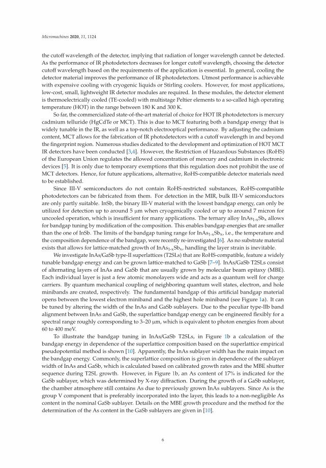
We investigate InAs/GaSb type-II superlattices (T2SLs) that are RoHS-compatible, feature a widelytunable bandgap energy and can be grown lattice-matched to GaSb [7–9]. InAs/GaSb T2SLs consistof alternating layers of InAs and GaSb that are usually grown by molecular beam epitaxy (MBE).Each individual layer is just a few atomic monolayers wide and acts as a quantum well for chargecarriers. By quantum mechanical coupling of neighboring quantum well states, electron, and holeminibands are created, respectively. The fundamental bandgap of this artificial bandgap materialopens between the lowest electron miniband and the highest hole miniband (see Figure 1a). It canbe tuned by altering the width of the InAs and GaSb sublayers. Due to the peculiar type-IIb bandalignment between InAs and GaSb, the superlattice bandgap energy can be engineered flexibly for aspectral range roughly corresponding to 3–20 μm, which is equivalent to photon energies from about60 to 400 meV.
To illustrate the bandgap tuning in InAs/GaSb T2SLs, in Figure 1b a calculation of thebandgap energy in dependence of the superlattice composition based on the superlattice empiricalpseudopotential method is shown [10]. Apparently, the InAs sublayer width has the main impact onthe bandgap energy. Commonly, the superlattice composition is given in dependence of the sublayerwidth of InAs and GaSb, which is calculated based on calibrated growth rates and the MBE shuttersequence during T2SL growth. However, in Figure 1b, an As content of 17% is indicated for theGaSb sublayer, which was determined by X-ray diffraction. During the growth of a GaSb sublayer,the chamber atmosphere still contains As due to previously grown InAs sublayers. Since As is thegroup V component that is preferably incorporated into the layer, this leads to a non-negligible Ascontent in the nominal GaSb sublayer. Details on the MBE growth procedure and the method for thedetermination of the As content in the GaSb sublayers are given in [10].
6
Micromachines 2020, 11, 1124
(a) (b)
Figure 1. (a) Schematic of the type-IIb band alignment between InAs and GaSb and an InAs/GaSbtype-II superlattice with lowest electron miniband and highest hole miniband. (b) Bandgap energyin dependence of the InAs/GaSb superlattice composition, calculated by the superlattice empiricalpseudopotential method [10].
After the proposal to use InAs/GaSb T2SLs for IR detection [11], fundamental research on thismaterial system [12,13] and development of single element detectors [14–16] and detector arrays [17]has intensified in the last decades. Important developmental steps in the field are reviewed in [18].
Activities in research and development of InAs/GaSb T2SLs have mainly focused onhigh-performance applications at low operating temperatures that require cryogenic cooling. As aresult, for low operating temperatures, InAs/GaSb T2SLs emerge as a viable alternative to MCT for IRdetectors and IR cameras. For the HOT range, IR detection with InAs/GaSb T2SLs in the longwaveinfrared was demonstrated [19–22], but dedicated device development and commercialization werenever conducted. Now, mainly due to the RoHS, there is renewed interest in InAs/GaSb T2SL IRphotodetectors for HOT applications.
Within the last few years, we have worked on the development of InAs/GaSb T2SL single elementdetectors for the HOT range and demonstrated that they can be combined with the immersion lenstechnology of VIGO system [23–25]. In this paper, we briefly describe the layout of the detector as alaterally-operated photoconductor, the superlattice and buffer layer growth as well as the detectorprocessing. Then, after the detector is integrated into an IR detector module with a four-stage TE-cooler,which allows for operation at 200 K, we focus on a possible spectroscopy application in which anMCT-based IR detector module could be replaced by a T2SL-based IR detector module.
In addition to the cutoff wavelength, two more detector figures of merit are crucial for the contentof this paper. The first is the specific detectivity D∗, which describes the signal-to-noise ratio:
D∗(λ, f ) =R(λ)In( f )
√AoΔ f . (1)
D∗ depends on the spectral responsivity R(λ), the noise current In( f ) and the bandwidth Δ f .It is normalized to the optical detector area Ao. By using a lens to focus incoming radiation, Ao canbe increased significantly. The increase depends on the form of the lens and its refractive index n.A hyperhemispheric lens can increase Ao by a factor of n4 [26]. For backside-illuminated detectors,the lens can be immersed into the substrate material beneath the detector. The second figure ofmerit is the detector bandwidth that relates to the detection speed. For the device concept understudy, the detector bandwidth is inversely proportional to the carrier recombination time. However,
7
Micromachines 2020, 11, 1124
the responsivity is proportional to the carrier recombination time. Therefore, there is a trade-offbetween photosignal and detection speed in photoconductor optimization.
2. Design, Growth, Processing and Module Integration of an IR Detector
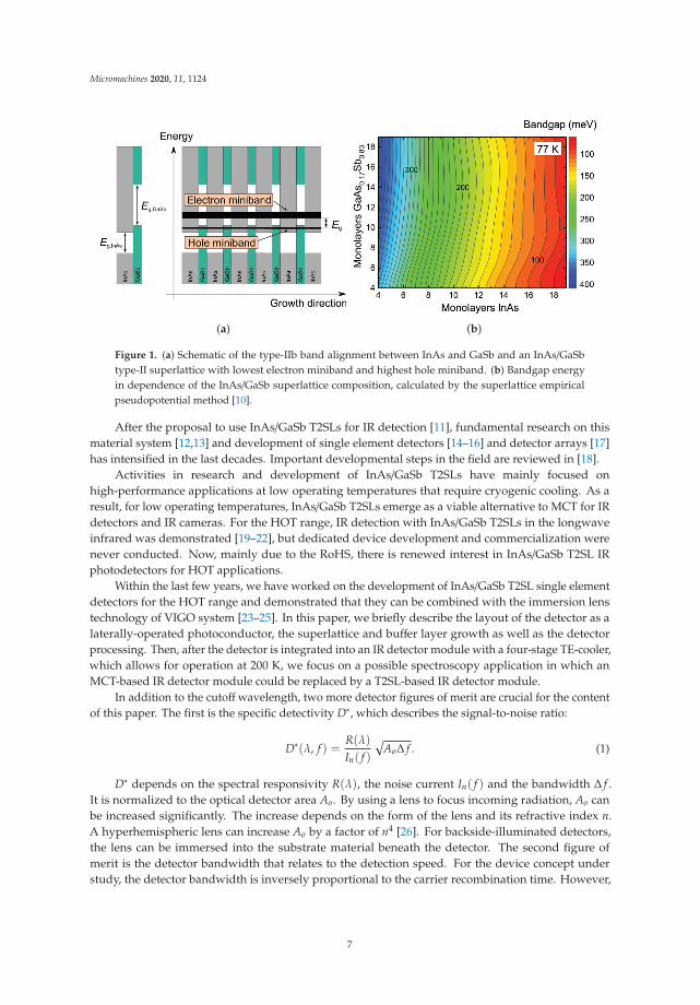
The InAs/GaSb T2SL discussed in this paper was grown by molecular beam epitaxy on a 3 inch,n-type, (100)-oriented, 1100 μm thick GaAs substrate after careful calibration of shutter sequencesand growth rates. Figure 2a shows the epitaxial layer structure. It consists of two buffer layers,the superlattice absorber layer and a thin superlattice contact layer. The first buffer layer is ametamorphic GaAsSb buffer, in which Sb gradually replaces As over 2 μm layer width. This results ina strain relaxed GaSb-like growth template for the subsequent layers [23]. The second buffer layerconsists of 10 μm GaSb. This layer is followed by the superlattice absorber layer, which comprises750 non-intentionally doped superlattice periods (residually n-type). Each of these periods features14 monolayers (ML) InAs and 7 ML GaSb. InSb-like interfacial layers were realized between theindividual InAs and GaSb sublayers to minimize the relative lattice mismatch to the underlyingsubstrate. In the end, the heavily n-type doped contact layer was grown on top.
(a) (b)
Figure 2. (a) Epitaxial layer structure for the fabrication of laterally-operated InAs/GaSb type-IIsuperlattice (T2SL) detectors on GaAs substrate. (b) Schematic of a processed InAs/GaSb T2SL detectorthat is backside-illuminated through an immersion lens (not to scale).
After growth, standard superlattice layer characterization was performed. A superlattice periodlength of 7.0 nm was determined by high-resolution X-ray diffraction, which was also used toverify the negligible relative lattice mismatch to the GaSb buffer. Spectral photoluminescencewas measured to confirm the intended bandgap energy. At 10 K, a bandgap energy of 143 meV(corresponding to a wavelength of 8.7 μm) was obtained. As the bandgap shrinks for rising temperature,which can be described with the Varshni model [25], the corresponding cutoffwavelength of a detectorincreases. Hence, this superlattice can absorb radiation throughout a large fraction of the MIR at highoperating temperatures.
Photolithographic processing was used to fabricate laterally-operated photoconductors (seeFigure 2b). Unlike in most T2SL-based detector concepts, in which the current flows parallel tothe superlattice growth direction, in this concept, the current flows mainly perpendicular to thegrowth direction between two ohmic metal contacts and requires external bias voltage for operation.When radiation of suitable wavelength enters the absorber layer, an additional photoconductivity isgenerated. The processing steps for detector fabrication included dry etching for structuring of thecontact and the absorber layer, dielectric passivation, selective opening of the passivation layer andmetalization. In the last step, the mesa front was also metalized. This metalized area acts as a mirrorfacilitating a double pass of the radiation incident from the backside, which increases the quantumefficiency. The processing sequence has been presented in more detail before [24].
A differing lattice constant of layer and substrate, which is the case for InAs/GaSb T2SLslattice matched to GaSb on GaAs substrates, may result in an increased density of defects, growth
8
Micromachines 2020, 11, 1124
inhomogeneities and a reduced device yield. Our wafer-level device characterization at 200 Ksuggested that device drop out due to material- or processing-related defects is negligible [24].As device performance proved to be homogeneous across the wafer, a large device yield would beexpected for manufacturing purposes. To allow for immersion of hyperhemispheric microlenses intothe substrate, the detectors were processed with a horizontal and vertical pitch of 1480 μm. In thisway, more than 1000 detectors could be fabricated per 3 inch wafer—the wafer size used in our study.Assuming the increasingly common 4 inch and 6 inch GaSb substrate diameters, the number of devicesper wafer would scale according to the wafer area. For fabrication of detectors without substratemicrolenses, the number of detectors per wafer depends on the intended detector size and can besignificantly higher.
After processing and the characterization of the T2SLs and the fabricated detectors, the fullyprocessed 3 inch wafers were diced into single element detectors. The module integration of thedetector elements was completed in cooperation with VIGO System. In these modules, a T2SLdetector 50 μm × 50 μm in size is mounted on top of a four-stage TE-cooler. The detectors featurea hyperhemispheric lens that was immersed into the GaAs substrate. As nGaAs ≈ 3.3, the lensincreases Ao for backside incident radiation by about two orders of magnitude and D∗ by one order ofmagnitude when compared to detector elements without such an immersion lens. Furthermore, the IRdetector modules also comprise standard electronics from VIGO System: a fast preamplifier and aTE-cooler controller. These TE-cooled T2SL-based IR detector modules constitute RoHS-compatibleturnkey systems.
3. Comparison to MCT
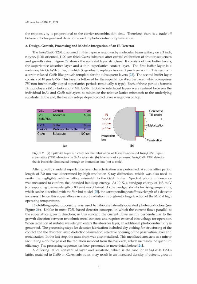
To benchmark the performance of these detectors, we compare the detectivity of MCT-basedand T2SL-based photoconductors without immersion lens. They are operated at 210 K with thenoise current taken at 20 kHz. In Figure 3, we show the mean value of the detectivity of InAs/GaSbT2SL photoconductors, which we deduced from measurements that were already discussed in [24].Here, we compare this mean value with specified detectivities of commercial MCT photoconductorsfrom VIGO System for different cutoffwavelengths from 9–13 μm [27]. For detectors with the samecutoff wavelength of 10.6 μm, the detectivity of the MCT photoconductor is less than a factor oftwo higher than the detectivity of the T2SL photoconductors. Given the brief development of HOTInAs/GaSb T2SL photodetectors in comparison to the longstanding heritage of MCT photodetectors,this is a highly promising result. Doping optimization [25] and increasing the quantum efficiency areexpected to further enhance the T2SL detector performance and increase its competitiveness.
Figure 3. Detectivity of InAs/GaSb T2SL photoconductors (mean value) and commercial mercurycadmium telluride (MCT) photoconductors from VIGO System (guaranteed values) for different cutoffwavelengths at 210 K and 20 kHz [24,27].
9
Micromachines 2020, 11, 1124
As a longer cutoff wavelength implies a lower bandgap and an increased carrier generation,which leads to an increased noise level, the peak detectivity of InAs/GaSb T2SL detectors is expectedto drop for longer cutoffwavelengths as it is the case for MCT-based detectors (see Figure 3). As thecutoff of an MCT detector crucially depends on the Cd content in the composition, which becomesmore challenging to control precisely and homogeneously towards longer cutoff wavelength, for moreelaborate device concepts the device yield drops and in turn the detector price rises. This drawbackdoes not exist for InAs/GaSb T2SLs.
4. Real-Time MIR Backscattering Spectroscopy System
In addition to our development of HOT InAs/GaSb T2SL IR detectors, we realized a demonstratorsystem for MIR backscattering spectroscopy. The operation principle of the demonstrator exploits thecharacteristic spectral diffuse reflection of solid chemical substances in the MIR that can be utilizedfor substance identification. Using a fast spectrally tunable quantum cascade laser (QCL) as theillumination source and a fast photodetector, the system is able to record IR spectra over more than250 cm−1 at rates of 1 kHz and therefore real-time spectroscopy. The high spectral scan speed ofthe system is ideal for fast changing scenarios or handheld operation as was demonstrated before.Here, we go beyond previous lab demonstrations of the measurement principle [28] as the system canrun constantly without user intervention for several hours.
4.1. Setup of the Demonstrator System
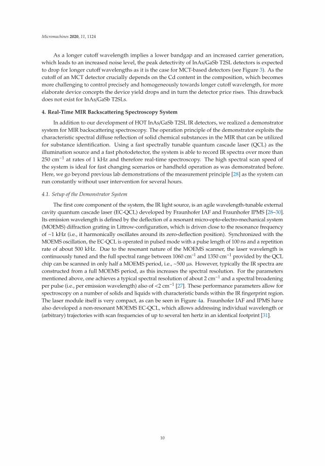
The first core component of the system, the IR light source, is an agile wavelength-tunable externalcavity quantum cascade laser (EC-QCL) developed by Fraunhofer IAF and Fraunhofer IPMS [28–30].Its emission wavelength is defined by the deflection of a resonant micro-opto-electro-mechanical system(MOEMS) diffraction grating in Littrow-configuration, which is driven close to the resonance frequencyof ~1 kHz (i.e., it harmonically oscillates around its zero-deflection position). Synchronized with theMOEMS oscillation, the EC-QCL is operated in pulsed mode with a pulse length of 100 ns and a repetitionrate of about 500 kHz. Due to the resonant nature of the MOEMS scanner, the laser wavelength iscontinuously tuned and the full spectral range between 1060 cm–1 and 1350 cm−1 provided by the QCLchip can be scanned in only half a MOEMS period, i.e., ~500 μs. However, typically the IR spectra areconstructed from a full MOEMS period, as this increases the spectral resolution. For the parametersmentioned above, one achieves a typical spectral resolution of about 2 cm−1 and a spectral broadeningper pulse (i.e., per emission wavelength) also of <2 cm−1 [27]. These performance parameters allow forspectroscopy on a number of solids and liquids with characteristic bands within the IR fingerprint region.The laser module itself is very compact, as can be seen in Figure 4a. Fraunhofer IAF and IPMS havealso developed a non-resonant MOEMS EC-QCL, which allows addressing individual wavelength or(arbitrary) trajectories with scan frequencies of up to several ten hertz in an identical footprint [31].
10
Micromachines 2020, 11, 1124
(a) (b)
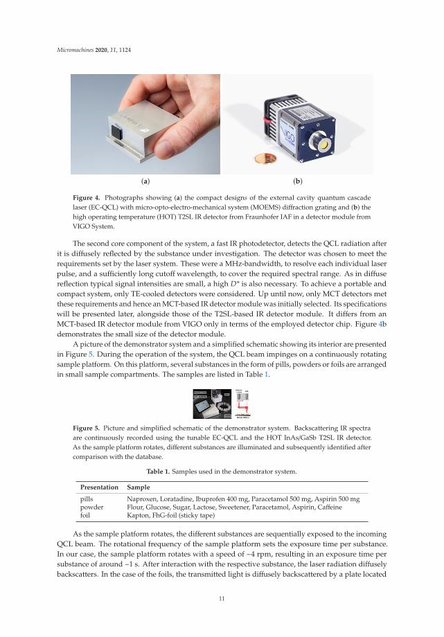
Figure 4. Photographs showing (a) the compact designs of the external cavity quantum cascadelaser (EC-QCL) with micro-opto-electro-mechanical system (MOEMS) diffraction grating and (b) thehigh operating temperature (HOT) T2SL IR detector from Fraunhofer IAF in a detector module fromVIGO System.
The second core component of the system, a fast IR photodetector, detects the QCL radiation afterit is diffusely reflected by the substance under investigation. The detector was chosen to meet therequirements set by the laser system. These were a MHz-bandwidth, to resolve each individual laserpulse, and a sufficiently long cutoff wavelength, to cover the required spectral range. As in diffusereflection typical signal intensities are small, a high D* is also necessary. To achieve a portable andcompact system, only TE-cooled detectors were considered. Up until now, only MCT detectors metthese requirements and hence an MCT-based IR detector module was initially selected. Its specificationswill be presented later, alongside those of the T2SL-based IR detector module. It differs from anMCT-based IR detector module from VIGO only in terms of the employed detector chip. Figure 4bdemonstrates the small size of the detector module.
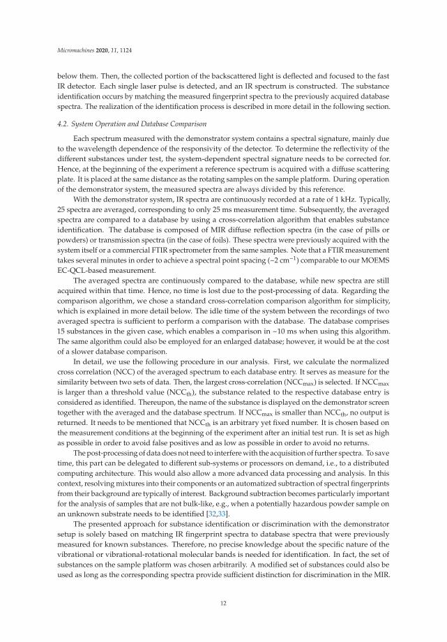
A picture of the demonstrator system and a simplified schematic showing its interior are presentedin Figure 5. During the operation of the system, the QCL beam impinges on a continuously rotatingsample platform. On this platform, several substances in the form of pills, powders or foils are arrangedin small sample compartments. The samples are listed in Table 1.
Figure 5. Picture and simplified schematic of the demonstrator system. Backscattering IR spectraare continuously recorded using the tunable EC-QCL and the HOT InAs/GaSb T2SL IR detector.As the sample platform rotates, different substances are illuminated and subsequently identified aftercomparison with the database.
Table 1. Samples used in the demonstrator system.
Presentation Sample
pills Naproxen, Loratadine, Ibuprofen 400 mg, Paracetamol 500 mg, Aspirin 500 mgpowder Flour, Glucose, Sugar, Lactose, Sweetener, Paracetamol, Aspirin, Caffeinefoil Kapton, FhG-foil (sticky tape)
As the sample platform rotates, the different substances are sequentially exposed to the incomingQCL beam. The rotational frequency of the sample platform sets the exposure time per substance.In our case, the sample platform rotates with a speed of ~4 rpm, resulting in an exposure time persubstance of around ~1 s. After interaction with the respective substance, the laser radiation diffuselybackscatters. In the case of the foils, the transmitted light is diffusely backscattered by a plate located
11
Micromachines 2020, 11, 1124
below them. Then, the collected portion of the backscattered light is deflected and focused to the fastIR detector. Each single laser pulse is detected, and an IR spectrum is constructed. The substanceidentification occurs by matching the measured fingerprint spectra to the previously acquired databasespectra. The realization of the identification process is described in more detail in the following section.
4.2. System Operation and Database Comparison
Each spectrum measured with the demonstrator system contains a spectral signature, mainly dueto the wavelength dependence of the responsivity of the detector. To determine the reflectivity of thedifferent substances under test, the system-dependent spectral signature needs to be corrected for.Hence, at the beginning of the experiment a reference spectrum is acquired with a diffuse scatteringplate. It is placed at the same distance as the rotating samples on the sample platform. During operationof the demonstrator system, the measured spectra are always divided by this reference.
With the demonstrator system, IR spectra are continuously recorded at a rate of 1 kHz. Typically,25 spectra are averaged, corresponding to only 25 ms measurement time. Subsequently, the averagedspectra are compared to a database by using a cross-correlation algorithm that enables substanceidentification. The database is composed of MIR diffuse reflection spectra (in the case of pills orpowders) or transmission spectra (in the case of foils). These spectra were previously acquired with thesystem itself or a commercial FTIR spectrometer from the same samples. Note that a FTIR measurementtakes several minutes in order to achieve a spectral point spacing (~2 cm−1) comparable to our MOEMSEC-QCL-based measurement.
The averaged spectra are continuously compared to the database, while new spectra are stillacquired within that time. Hence, no time is lost due to the post-processing of data. Regarding thecomparison algorithm, we chose a standard cross-correlation comparison algorithm for simplicity,which is explained in more detail below. The idle time of the system between the recordings of twoaveraged spectra is sufficient to perform a comparison with the database. The database comprises15 substances in the given case, which enables a comparison in ~10 ms when using this algorithm.The same algorithm could also be employed for an enlarged database; however, it would be at the costof a slower database comparison.
In detail, we use the following procedure in our analysis. First, we calculate the normalizedcross correlation (NCC) of the averaged spectrum to each database entry. It serves as measure for thesimilarity between two sets of data. Then, the largest cross-correlation (NCCmax) is selected. If NCCmax
is larger than a threshold value (NCCth), the substance related to the respective database entry isconsidered as identified. Thereupon, the name of the substance is displayed on the demonstrator screentogether with the averaged and the database spectrum. If NCCmax is smaller than NCCth, no output isreturned. It needs to be mentioned that NCCth is an arbitrary yet fixed number. It is chosen based onthe measurement conditions at the beginning of the experiment after an initial test run. It is set as highas possible in order to avoid false positives and as low as possible in order to avoid no returns.
The post-processing of data does not need to interfere with the acquisition of further spectra. To savetime, this part can be delegated to different sub-systems or processors on demand, i.e., to a distributedcomputing architecture. This would also allow a more advanced data processing and analysis. In thiscontext, resolving mixtures into their components or an automatized subtraction of spectral fingerprintsfrom their background are typically of interest. Background subtraction becomes particularly importantfor the analysis of samples that are not bulk-like, e.g., when a potentially hazardous powder sample onan unknown substrate needs to be identified [32,33].
The presented approach for substance identification or discrimination with the demonstratorsetup is solely based on matching IR fingerprint spectra to database spectra that were previouslymeasured for known substances. Therefore, no precise knowledge about the specific nature of thevibrational or vibrational-rotational molecular bands is needed for identification. In fact, the set ofsubstances on the sample platform was chosen arbitrarily. A modified set of substances could also beused as long as the corresponding spectra provide sufficient distinction for discrimination in the MIR.
12
Micromachines 2020, 11, 1124
4.3. Detector Module Interchangeability
To demonstrate the applicability of the T2SL-based IR module for spectroscopy, we replaced theMCT-based IR detector module in the demonstrator system with the T2SL-based IR detector module.The MCT-based module features a two-stage TE-cooled, photovoltaic IR detector that is illuminatedvia a hemispheric lens resulting in an optical area of 1 mm × 1 mm. This module has been specifiedwith a cutoffwavelength of 10.6 μm, a bandwidth of 100 MHz and a detectivity of 6.8 × 108 cm
√Hz/W.
The T2SL-based module features a four-stage TE-cooled, photoconductive, 50 μm × 50 μm-sized IRdetector that is illuminated via a hyperhemispheric lens, resulting in an optical area of approximately500 μm × 500 μm. It has been specified with a cutoffwavelength of 9.3 μm, a bandwidth of 10 MHzand a detectivity of 6.7 × 109 cm
√Hz/W. The specifications of both detectors are listed in Table 2.
Table 2. Specifications of the two IR detector modules, based on an MCT detector and an InAs/GaSbT2SL detector, respectively.
MCT InAs/GaSb T2SL
Detectivity 6.8 × 108 cm√
Hz/W 6.7 × 109 cm√
Hz/WBandwidth 100 MHz 10 MHzCutoffWavelength 10.6 μm 9.3 μmOperating temperature 226 K (2-stage TEC) 200 K (4-stage TEC)Operation mode photovoltaic photoconductiveOptical Area 1 mm × 1 mm 0.5 mm × 0.5 mmLens hemispheric hyperhemispheric
As both modules feature equal packages and housings from VIGO System, replacing theMCT-based detector module, integrating the T2SL-based IR detector module into the setup andits optical alignment were straightforward. In the following, we report on the operation of thedemonstrator system with both IR detector modules.
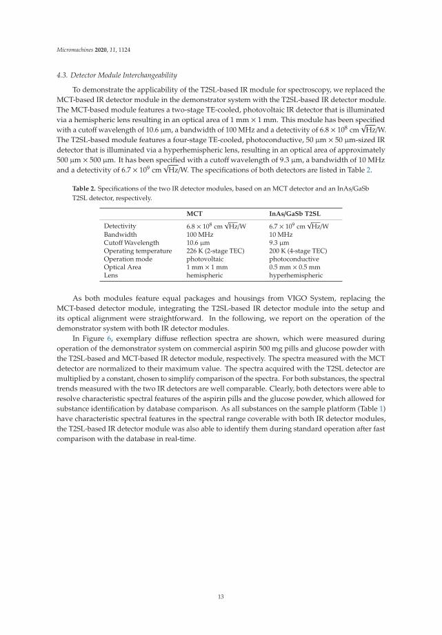
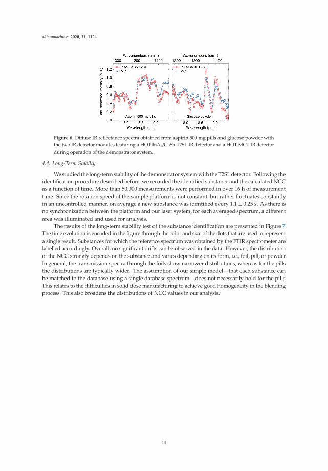
In Figure 6, exemplary diffuse reflection spectra are shown, which were measured duringoperation of the demonstrator system on commercial aspirin 500 mg pills and glucose powder withthe T2SL-based and MCT-based IR detector module, respectively. The spectra measured with the MCTdetector are normalized to their maximum value. The spectra acquired with the T2SL detector aremultiplied by a constant, chosen to simplify comparison of the spectra. For both substances, the spectraltrends measured with the two IR detectors are well comparable. Clearly, both detectors were able toresolve characteristic spectral features of the aspirin pills and the glucose powder, which allowed forsubstance identification by database comparison. As all substances on the sample platform (Table 1)have characteristic spectral features in the spectral range coverable with both IR detector modules,the T2SL-based IR detector module was also able to identify them during standard operation after fastcomparison with the database in real-time.
13
Micromachines 2020, 11, 1124
Figure 6. Diffuse IR reflectance spectra obtained from aspirin 500 mg pills and glucose powder withthe two IR detector modules featuring a HOT InAs/GaSb T2SL IR detector and a HOT MCT IR detectorduring operation of the demonstrator system.
4.4. Long-Term Stabilty
We studied the long-term stability of the demonstrator system with the T2SL detector. Following theidentification procedure described before, we recorded the identified substance and the calculated NCCas a function of time. More than 50,000 measurements were performed in over 16 h of measurementtime. Since the rotation speed of the sample platform is not constant, but rather fluctuates constantlyin an uncontrolled manner, on average a new substance was identified every 1.1 ± 0.25 s. As there isno synchronization between the platform and our laser system, for each averaged spectrum, a differentarea was illuminated and used for analysis.
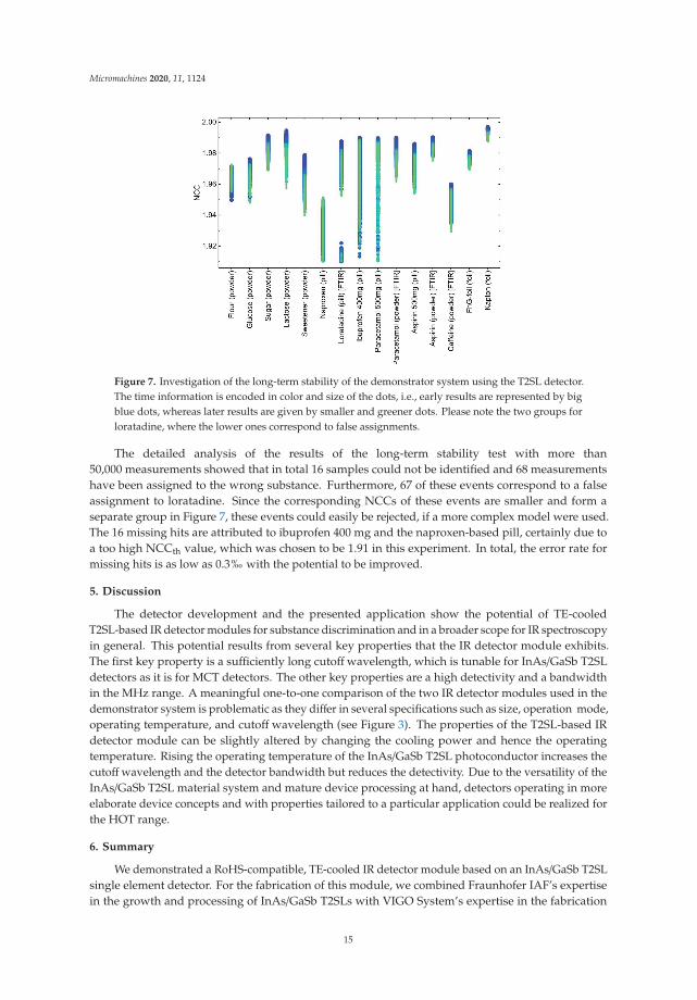
The results of the long-term stability test of the substance identification are presented in Figure 7.The time evolution is encoded in the figure through the color and size of the dots that are used to representa single result. Substances for which the reference spectrum was obtained by the FTIR spectrometer arelabelled accordingly. Overall, no significant drifts can be observed in the data. However, the distributionof the NCC strongly depends on the substance and varies depending on its form, i.e., foil, pill, or powder.In general, the transmission spectra through the foils show narrower distributions, whereas for the pillsthe distributions are typically wider. The assumption of our simple model—that each substance canbe matched to the database using a single database spectrum—does not necessarily hold for the pills.This relates to the difficulties in solid dose manufacturing to achieve good homogeneity in the blendingprocess. This also broadens the distributions of NCC values in our analysis.
14
Micromachines 2020, 11, 1124
Figure 7. Investigation of the long-term stability of the demonstrator system using the T2SL detector.The time information is encoded in color and size of the dots, i.e., early results are represented by bigblue dots, whereas later results are given by smaller and greener dots. Please note the two groups forloratadine, where the lower ones correspond to false assignments.
The detailed analysis of the results of the long-term stability test with more than50,000 measurements showed that in total 16 samples could not be identified and 68 measurementshave been assigned to the wrong substance. Furthermore, 67 of these events correspond to a falseassignment to loratadine. Since the corresponding NCCs of these events are smaller and form aseparate group in Figure 7, these events could easily be rejected, if a more complex model were used.The 16 missing hits are attributed to ibuprofen 400 mg and the naproxen-based pill, certainly due toa too high NCCth value, which was chosen to be 1.91 in this experiment. In total, the error rate formissing hits is as low as 0.3‰ with the potential to be improved.
5. Discussion
The detector development and the presented application show the potential of TE-cooledT2SL-based IR detector modules for substance discrimination and in a broader scope for IR spectroscopyin general. This potential results from several key properties that the IR detector module exhibits.The first key property is a sufficiently long cutoffwavelength, which is tunable for InAs/GaSb T2SLdetectors as it is for MCT detectors. The other key properties are a high detectivity and a bandwidthin the MHz range. A meaningful one-to-one comparison of the two IR detector modules used in thedemonstrator system is problematic as they differ in several specifications such as size, operation mode,operating temperature, and cutoff wavelength (see Figure 3). The properties of the T2SL-based IRdetector module can be slightly altered by changing the cooling power and hence the operatingtemperature. Rising the operating temperature of the InAs/GaSb T2SL photoconductor increases thecutoff wavelength and the detector bandwidth but reduces the detectivity. Due to the versatility of theInAs/GaSb T2SL material system and mature device processing at hand, detectors operating in moreelaborate device concepts and with properties tailored to a particular application could be realized forthe HOT range.
6. Summary
We demonstrated a RoHS-compatible, TE-cooled IR detector module based on an InAs/GaSb T2SLsingle element detector. For the fabrication of this module, we combined Fraunhofer IAF’s expertisein the growth and processing of InAs/GaSb T2SLs with VIGO System’s expertise in the fabrication
15
Micromachines 2020, 11, 1124
of TE-cooled IR detector modules. This paper shows that this T2SL-based IR detector module anda commercial MCT-based IR detector module can be employed interchangeably in a compact andreal-time MIR backscattering spectroscopy system. This system provides a very low error rate of only0.3‰ in substance differentiation, which can be further improved. Furthermore, we showed that forequal operation mode, operating temperature, cutoff wavelength, and noise frequency, the detectivityof photoconductors based on InAs/GaSb T2SLs and MCT is comparable. This renders InAs/GaSbT2SLs promising for fully RoHS-compatible HOT IR photodetectors.
Author Contributions: Conceptualization, growth, and processing of the IR detector, R.M., J.N., V.D. and R.R.;conceptualization of the laser demonstrator, K.S. and M.H.; methodology, R.M. and M.H.; validation, Y.V.F.and K.S.; data curation, R.M.; writing—original draft preparation, R.M.; writing—review and editing, R.R.,Y.V.F. and M.H.; visualization, R.M.; supervision, R.R. and R.O.; project administration, R.R. and R.O.; fundingacquisition, R.R. and R.O. All authors have read and agreed to the published version of the manuscript.
Funding: This research was funded by the Horizon 2020 Research and Innovation program under grant agreementno. 688265.
Acknowledgments: The authors thank Peter Holl and Stefan Hugger for developmental work (both withFraunhofer IAF). We acknowledge the support from VIGO System during the developmental phase of HOTInAs/GaSb T2SL IR photoconductors, including detector characterization (Figure 3). Furthermore, we are gratefulto VIGO System for the module integration of our HOT InAs/GaSb T2SL IR detectors.
Conflicts of Interest: The authors declare no conflict of interest. The funders had no role in the design of thestudy; in the collection, analyses, or interpretation of data; in the writing of the manuscript, or in the decision topublish the results.
References
1. Lambrecht, A.; Schmitt, K. Mid-infrared gas-sensing systems and applications. In Mid-Infrared Optoelectronics:Materials, Devices, and Applications; Tournié, E., Cerutti, L., Eds.; Elsevier Science & Technology:Amsterdam, The Netherlands, 2007; pp. 661–715. [CrossRef]
2. Schwaighofer, A.; Brandstetter, M.; Lendl, B. Quantum cascade lasers (QCLs) in biomedical spectroscopy.Chem. Soc. Rev. 2017, 46, 5903–5924. [CrossRef] [PubMed]
3. Piotrowski, J.; Galus, W.; Grudzien, M. Near room-temperature IR photo-detectors. Infrared Phys. 1991,31, 1–48. [CrossRef]
4. Kalinowski, P.; Mikołajczyk, J.; Piotrowski, A.; Piotrowski, J. Recent advances in manufacturing ofminiaturized uncooled IR detection modules. Semicond. Sci. Technol. 2019, 34, 033002. [CrossRef]
5. Directive 2011/65/EU of the European Parliament and of the Council “RoHS-Restriction”. Available online:https://eur-lex.europa.eu/legal-content/En/TXT/?uri=celex%3A32011L0065 (accessed on 15 December 2020).
6. Murawski, K.; Gomolka, E.; Kopytko, M.; Grodecki, K.; Michalczewski, K.; Kubiszyn, L.; Gawron, W.;Martyniuk, P.; Rogalski, A.; Piotrowski, J. Bandgap energy determination of InAsSb epilayers grown bymolecular beam epitaxy on GaAs substrates. Prog. Nat. Sci. Mater. Int. 2019, 29, 472–476. [CrossRef]
7. Sai-Halasz, G.A.; Tsu, R.; Esaki, L. A new semiconductor superlattice. Appl. Phys. Lett. 1977, 30, 651–653.[CrossRef]
8. Sai-Halasz, G.A.; Esaki, L.; Harrison, W.A. InAs-GaSb superlattice energy structure and itssemiconductor-semimetal transition. Phys. Rev. B 1978, 18, 2812–2818. [CrossRef]
9. Sai-Halasz, G.A.; Chang, L.; Welter, J.-M.; Chang, C.-A.; Esaki, L. Optical absorption of In1 xGaxAs/GaSb1yAsy superlattices. Solid State Commun. 1978, 27, 935–937. [CrossRef]
10. Masur, J.-M.; Rehm, R.; Schmitz, J.; Kirste, L.; Walther, M. Four-component superlattice empiricalpseudopotential method for InAs/GaSb superlattices. Infrared Phys. Technol. 2013, 61, 129–133. [CrossRef]
11. Smith, D.L.; Mailhiot, C. Proposal for strained type II superlattice infrared detectors. J. Appl. Phys. 1987,62, 2545–2548. [CrossRef]
12. Herres, N.; Fuchs, F.; Schmitz, J.; Pavlov, K.M.; Wagner, J.; Ralston, J.D.; Koidl, P.; Gadaleta, C.; Scamarcio, G.Effect of interfacial bonding on the structural and vibrational properties of InAs/GaSb superlattices.Phys. Rev. B 1996, 53, 15688. [CrossRef]
16
Micromachines 2020, 11, 1124
13. Umana-Membreno, G.A.; Klein, B.; Kala, H.; Antoszewski, J.; Gautam, N.; Kutty, M.N.; Plis, E.;Krishna, S.; Faraone, L. Vertical minority carrier electron transport in p-type InAs/GaSb type-II superlattices.Appl. Phys. Lett. 2012, 101, 253515. [CrossRef]
14. Johnson, J.L.; Samoska, L.A.; Gossard, A.C.; Merz, J.L.; Jack, M.D.; Chapman, G.R.; Baumgartz, B.A.;Kosai, K.; Johnson, S.M. Electrical and optical properties of infrared photodiodes using the InAs/Ga1-xInxSbsuperlattice in heterojunctions with GaSb. J. Appl. Phys. 1996, 80, 1116–1127. [CrossRef]
15. Fuchs, F.; Weimer, U.; Pletschen, W.; Schmitz, J.; Ahlswede, E.; Walter, M.; Wagner, J.; Koidl, P.High performance InAs/Ga1-xInxSb superlattice infrared photodiodes. Appl. Phys. Lett. 1997, 71, 3251–3253.[CrossRef]
16. Ting, D.; Hill, C.J.; Soibel, A.; Keo, S.A.; Mumolo, J.M.; Nguyen, J.; Gunapala, S.D. A high-performancelong wavelength superlattice complementary barrier infrared detector. Appl. Phys. Lett. 2009, 95, 023508.[CrossRef]
17. Walther, M.; Rehm, R.; Fuchs, F.; Schmitz, J.; Fleißner, J.; Cabanski, W.; Eich, D.; Finck, M.; Rode, W.;Wendler, J.; et al. 256 × 256 focal plane array midwavelength infrared camera based on InAs/GaSbshort-period superlattices. J. Electron. Mater. 2005, 34, 722–725. [CrossRef]
18. Ting, D.; Soibel, A.; Höglund, L.; Nguyen, J.; Hill, C.J.; Khoshakhlagh, A.; Gunapala, S.D. Type-II SuperlatticeInfrared Detectors. In Semiconductors and Semimetals; Gunapala, S.D., Rhiger, D.R., Jagadish, C., Eds.;Academic Press: San Diego, CA, USA, 2011; Volume 84, pp. 1–57.
19. Mohseni, H.; Litvinov, V.I.; Razeghi, M. Interface-induced suppression of the Auger recombination in type-IIInAs/GaSb superlattices. Phys. Rev. B 1998, 58, 15378–15380. [CrossRef]
20. Mohseni, H.; Razeghi, M. Long-wavelength type-II photodiodes operating at room temperature.IEEE Photonics Technol. Lett. 2001, 13, 517–519. [CrossRef]
21. Mohseni, H.; Michel, E.; Sandoen, J.; Razeghi, M.; Mitchel, W.; Brown, G. Growth and characterization ofInAs/GaSb photoconductors for long wavelength infrared range. Appl. Phys. Lett. 1997, 71, 1403–1405.[CrossRef]
22. Mohseni, H.; Wojkowski, J.; Razeghi, M.; Brown, G.; Mitchel, W. Uncooled InAs-GaSb type-II infrareddetectors grown on GaAs substrates for the 8-12-μm atmospheric window. IEEE J. Quantum Electron. 1999,35, 1041–1044. [CrossRef]
23. Müller, R.; Gramich, V.; Wauro, M.; Niemasz, J.; Kirste, L.; Daumer, V.; Janaszek, A.; Jurenczyk, J.; Rehm, R.High operating temperature InAs/GaSb type-II superlattice detectors on GaAs substrate for the longwavelength infrared. Infrared Phys. Technol. 2019, 96, 141–144. [CrossRef]
24. Müller, R.; Niemasz, J.; Daumer, V.; Janaszek, A.; Jurenczyk, J.; Rehm, R. Advances on photoconductiveInAs/GaSb type-II superlattice long-wavelength infrared detectors for high operating temperature. Proc. SPIE2019, 10914, 1091416. [CrossRef]
25. Müller, R.; Niemasz, J.; Daumer, V.; Rehm, R. Design guidelines for high operating temperature InAs/GaSbtype-II superlattice photoconductors for the longwave infrared. (to be published).
26. Piotrowski, J.; Rogalski, A. High-Operating-Temperature Infrared Photodetectors; SPIE Press: Bellingham, WA, USA,2007; p. 28.
27. VIGO System Homepage. Available online: https://vigo.com.pl/produkty/pc-3te/ (accessed on 15 May 2020).28. Butschek, L.; Hugger, S.; Jarvis, J.; Härtelt, M.; Merten, A.; Schwarzenberg, M.; Grahmann, J.; Stothard, D.M.;
Warden, M.; Carson, C.; et al. Microoptoelectromechanical systems-based external cavity quantum cascadelasers for real-time spectroscopy. Opt. Eng. 2017, 57, 011010. [CrossRef]
29. Grahmann, J.; Merten, A.; Ostendorf, R.; Fontenot, M.; Bleh, D.; Schenk, H.; Wagner, H.-J. Tunable ExternalCavity Quantum Cascade Lasers (EC-QCL): An application field for MOEMS based scanning gratings.Proc. SPIE 2014, 8977, 897708. [CrossRef]
30. Ostendorf, R.; Butschek, L.; Hugger, S.; Fuchs, F.; Yang, Q.; Jarvis, J.; Schilling, C.; Rattunde, M.; Merten, A.;Grahmann, J.; et al. Recent advances and applications of external cavity-QCLs towards hyperspectralimaging for standoff detection and real-time spectroscopic sensing of chemicals. Photonics 2016, 3, 28.[CrossRef]
31. Haertelt, M.; Hugger, S.; Butschek, L.; Schilling, C.; Merten, A.; Schwarzenberg, M.; Dreyhaupt, A.;Grahmann, J.; Rattunde, M.; Ostendorf, R. Advances of MOEMS-based external cavity QCLs. Proc. SPIE2019, 10926, 1092613. [CrossRef]
17

Micromachines 2020, 11, 1124
32. Jarvis, J.; Fuchs, F.; Hugger, S.; Ostendorf, R.; Butschek, L.; Yang, Q.; Dreyhaupt, A.; Grahmann, J.; Wagner, J.Hyperspectral image analysis for standoff trace detection using IR laser spectroscopy. Proc. SPIE 2016,9824, 98240V. [CrossRef]
33. Jarvis, J.; Haertelt, M.; Hugger, S.; Butschek, L.; Fuchs, F.; Ostendorf, R.; Wagner, J.; Beyerer, J.Hyperspectral data acquisition and analysis in imaging and real-time active MIR backscattering spectroscopy.Adv. Opt. Technol. 2017, 6, 85–93. [CrossRef]
Publisher’s Note: MDPI stays neutral with regard to jurisdictional claims in published maps and institutionalaffiliations.
© 2020 by the authors. Licensee MDPI, Basel, Switzerland. This article is an open accessarticle distributed under the terms and conditions of the Creative Commons Attribution(CC BY) license (http://creativecommons.org/licenses/by/4.0/).
18
micromachines
Article
Manganite Heterojunction Photodetector with BroadSpectral Response Range from 200 nm to 2 μm
Ru Chen 1, Zhiqing Lu 2 and Kun Zhao 1,*
1 College of New Energy and Materials, China University of Petroleum (Beijing), Beijing 102249, China;[email protected]
2 College of Sciences, China University of Petroleum (Beijing), Beijing 102249, China; [email protected]* Correspondence: [email protected]; Tel.: +86-10-89734836
Received: 19 December 2019; Accepted: 16 January 2020; Published: 23 January 2020
Abstract: In this paper, we investigate the broad spectral photocurrent properties of theLa0.67Ca0.33MnO3/Si (LCMO/Si) heterojunction from 200 nm to 2.0 μm, as the temperature increasesfrom 95 to 300 K. We observed the junction’s uniform responsivity in the visible range and fiveabsorption peaks at 940 nm, 1180 nm, 1380 nm, 1580 nm, and 1900 nm wavelengths. The temperatureshowed effective affection to the photocurrents at absorption peaks and the transition point occurredat 216 K, which was also displayed in the temperature dependence of junction resistance. On thebasis of the results, we propose a possible model involving the quantum size effect at the junctioninterface as the mechanism. This understanding of the infrared photodetection properties of oxideheterostructures should open a route for devising future microelectronic devices.
Keywords: manganite; heterostructure; photodetector
1. Introduction
Oxide semiconductor devices based on the perovskite oxide films, whose properties can becontrolled by magnetic field, electric field, and light irradiation, have attracted a great deal of interest.Experiments confirmed that manganite-based perovskite-type oxides have excellent ultraviolet (UV)photoresponse characteristics with ultrafast response-time of picosecond and high sensitivity, whichmakes this class of materials potentially useful for UV sensor applications [1,2]. Furthermore, manganiteheterojunctions offer the features of tunability by magnetic and electric fields, high-sensitivity tolight illumination and high carrier mobility, suggesting many possible applications and researchdirections including information storage, optoelectronics information processing, and advancedsample preparation techniques associated with microstructure modulate research [3–7]. In addition,similar to many optical materials with chemical stability, manganite heterojunctions are insensitive toharsh physical environment such as fluctuations of temperature and pressure, suggesting a potentialapplication of manganite heterojunction photodetectors in harsh environments for the need of oil andgas optics [8–12]. Integrating the perovskite-type transition metal oxides with the silicon (Si)-basedsemiconductor technology would also introduce the possibility for a multifunctional microelectronicdevice [13–15].
Si photodetectors have already found wide acceptance for visible light applications, while it hassmall absorption coefficient in near-infrared (NIR) wavelength range because of the cut offwavelengthof ~1100 nm. Now most NIR photodetectors were composed of PbS, PbSe, or InGaAs. The toxicprecursors, such as Pb, Se, and As, was usually used to synthesize these materials. It is a meaningfulthing to find non-toxic and pollution-free material for photodetector working at NIR wavelength range.
The infrared (IR) spectrum has become an important method to study the lattice distortionand been applied to investigate the photoconductive effect in perovskite manganese oxides, where
Micromachines 2020, 11, 129; doi:10.3390/mi11020129 www.mdpi.com/journal/micromachines19
Micromachines 2020, 11, 129
mid-infrared or far-infrared spectra was used to explain the complex physical process in manganitessuch as the electronic transition, electron-phonon interaction, coupling between lattice, orbital, andspin, etc., [16–22]. In this paper the photocurrent response spectrum between 200 nm and 2 μmof the heterojunction La0.67Ca0.33MnO3/Si (LCMO/Si) is reported. The temperature dependence ofthe photocurrent response of the sample was investigated to reveal more information related to thephotoelectric response, and selective absorption peaks were observed. The mechanism about theresults is also discussed in the paper.
2. Materials and Methods
The LCMO/Si heterojunction was fabricated using the facing target sputtering technique. A 100 nmthickness LCMO layer was grown on a 0.5 mm thick n-type Si (001) wafer. The wafer temperature waskept at 680 ◦C with the oxygen pressure being 60 mTorr during deposition. Immediately after eachdeposition, the vacuum chamber was back-filled with 1 atm oxygen gas.
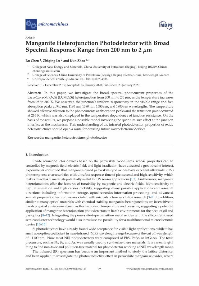
The photocurrent of the sample was detected by the spectral response measurement system,as shown in Figure 1. The system was designed to measure the UV and IR spectral responsivitycharacteristics of samples in low temperature environment. The operation was automaticallycontrolled, and the system maintained good closure during the measurement process. The selectedall-reflected-light-route system, UV, visible light or IR, can be switched automatically with maximumlight path coupling efficiency. The diameter of the light spot was 3 mm. The light intensity wascalibrated using the spectrum of a commercial UV-100L Si photodiode (from OSI Systems Inc.,Hawthorne, CA, USA) and the spectral responsivity was measured by a monochromator.
Figure 1. Spectral response measurement system.
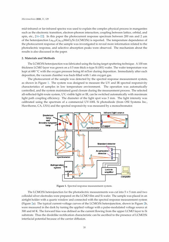
The LCMO/Si heterojunction for the photoelectric measurements was cut into 5 × 5 mm and twocolloidal silver electrodes were prepared on the LCMO film and Si wafer. The sample was placed in anairtight holder with a quartz window and connected with the spectral response measurement system(Figure 2a). The typical current-voltage curves of the LCMO/Si heterojunction, shown in Figure 2b,were measured in the dark by tuning the applied voltage with a pulse-modulated voltage source at300 and 60 K. The forward bias was defined as the current flowing from the upper LCMO layer to Sisubstrate. Thus the diodelike rectification characteristic can be ascribed to the presence of LCMO/Siinterfacial potential because of the carrier diffusion.
20
Micromachines 2020, 11, 129
Figure 2. (a) The setup of La0.67Ca0.33MnO3/Si (LCMO/Si) heterojunction for the spectral responsemeasurement. (b) The current-voltage curves of the LCMO/Si heterojunction at 300 and 60 K.
3. Results and Discussions
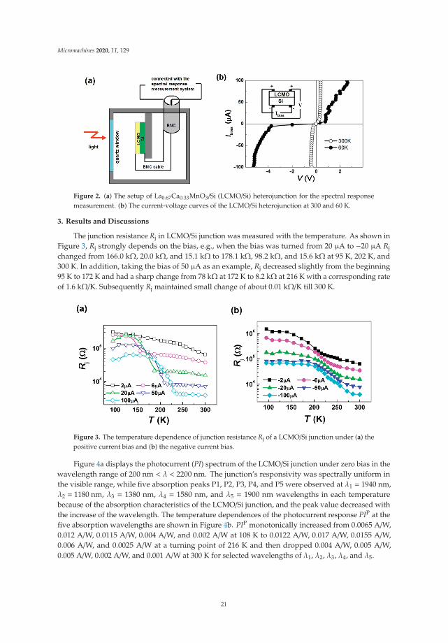
The junction resistance Rj in LCMO/Si junction was measured with the temperature. As shown inFigure 3, Rj strongly depends on the bias, e.g., when the bias was turned from 20 μA to −20 μA Rj
changed from 166.0 kΩ, 20.0 kΩ, and 15.1 kΩ to 178.1 kΩ, 98.2 kΩ, and 15.6 kΩ at 95 K, 202 K, and300 K. In addition, taking the bias of 50 μA as an example, Rj decreased slightly from the beginning95 K to 172 K and had a sharp change from 78 kΩ at 172 K to 8.2 kΩ at 216 K with a corresponding rateof 1.6 kΩ/K. Subsequently Rj maintained small change of about 0.01 kΩ/K till 300 K.
Figure 3. The temperature dependence of junction resistance Rj of a LCMO/Si junction under (a) thepositive current bias and (b) the negative current bias.
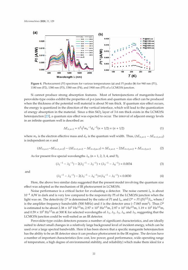
Figure 4a displays the photocurrent (PI) spectrum of the LCMO/Si junction under zero bias in thewavelength range of 200 nm < λ < 2200 nm. The junction’s responsivity was spectrally uniform inthe visible range, while five absorption peaks P1, P2, P3, P4, and P5 were observed at λ1 = 1940 nm,λ2 = 1180 nm, λ3 = 1380 nm, λ4 = 1580 nm, and λ5 = 1900 nm wavelengths in each temperaturebecause of the absorption characteristics of the LCMO/Si junction, and the peak value decreased withthe increase of the wavelength. The temperature dependences of the photocurrent response PIP at thefive absorption wavelengths are shown in Figure 4b. PIP monotonically increased from 0.0065 A/W,0.012 A/W, 0.0115 A/W, 0.004 A/W, and 0.002 A/W at 108 K to 0.0122 A/W, 0.017 A/W, 0.0155 A/W,0.006 A/W, and 0.0025 A/W at a turning point of 216 K and then dropped 0.004 A/W, 0.005 A/W,0.005 A/W, 0.002 A/W, and 0.001 A/W at 300 K for selected wavelengths of λ1, λ2, λ3, λ4, and λ5.
21
Micromachines 2020, 11, 129
Figure 4. Photocurrent (PI) spectrum for various temperatures (a) and PI peaks (b) for 940 nm (P1),1180 nm (P2), 1380 nm (P3), 1580 nm (P4), and 1900 nm (P5) of a LCMO/Si junction.
Si cannot produce strong absorption features. Most of heterojunctions of manganite-basedperovskite-type oxides exhibit the properties of p-n junction and quantum size effect can be producedwhen the thickness of the potential well material is about 50 nm thick. If quantum size effect occurs,the energy is quantized in the direction of the vertical interface, which will lead to the quantizationof energy absorption in the material. Since a thin SiO2 layer of 3.6 nm thick exists in the LCMO/Siheterojunction [23], a quantum size effect was expected to occur. The interval of adjacent energy levelsin an infinite quantum well is described as:
ΔEn,n+1 = π2η2mn
−1dw−2(n + 1/2) ∝ (n + 1/2) (1)
where mn is the electron effective mass and dw is the quantum well width. Thus, (ΔEn,n+1 − ΔEn+1,n+2)is independent on n and
(ΔEn,n+1−ΔEn+1,n+2) − (ΔEn+1,n+2 − ΔEn+2,n+3) ≈ ΔEn,n+1 − 2ΔEn+1,n+2 + ΔEn+2,n+3 (2)
As for present five special wavelengths λn (n = 1, 2, 3, 4, and 5),
(λ1−1 − λ2
−1) − 2(λ2−1 − λ3
−1) + (λ3−1 − λ4
−1) ≈ 0.0034 (3)
and(λ2−1 − λ3
−1) − 2(λ3−1 − λ4
−1)+(λ4−1 − λ5
−1) ≈ 0.0030 (4)
Here, the above two similar data suggested that the present model involving the quantum sizeeffect was adopted as the mechanism of IR photocurrent in LCMO/Si.
Noise performance is a critical factor for evaluating a detector. The noise current In is about10−4 A/W in dark and is very low compared to the responsivity PI of the LCMO/Si junction when thelight was on. The detectivity D* is determined by the ratio of PI and In, and D* = PI (fS)1/2/In, where fis the amplifier frequency bandwidth (500 MHz) and S is the detector area (~7.065 mm2). Thus D*is estimated to be about 2.38 × 10³ Hz1/2m, 2.97 × 10³ Hz1/2m, 2.97 × 10³ Hz1/2m, 1.19 × 10³ Hz1/2m,and 0.59 × 10³ Hz1/2m at 300 K for selected wavelengths of λ1, λ2, λ3, λ4, and λ5, suggesting that theLCMO/Si junction could be well-suited as an IR detector.
Perovskite-type oxides detectors possess a number of significant characteristics, and are ideallysuited to detect small changes in a relatively large background level of incident energy, which can beused over a large spectral bandwidth. Here it has been shown that a specific manganite heterojunctionhas the ability to be an IR detector since it can produce photocurrent in the IR regime. The devices havea number of important characteristics (low cost, low power, good performance, wide operating rangeof temperature, a high degree of environmental stability, and reliability) which make them ideal for a
22
Micromachines 2020, 11, 129
range of applications from consumer and commercial to military requirements. LCMO/Si junction is anew material for photodetector fabrication compared to traditional materials. It is anticipated thatmanganite heterojunction IR detectors will assume an ever growing importance in our society over thenext few years.
4. Conclusions
In conclusion, we fabricated a manganite-based heterojunction by depositing a LCMO thin filmon the Si substrate. The broad spectral photocurrent effect of the junction was systematically studiedin a temperature range from 95 to 300 K. The responsivity of LCMO/Si heterojunction was spectrallyuniform in the visible range. Five absorption peaks occurred at 940 nm, 1180 nm, 1380 nm, 1580 nm, and1900 nm in the IR range, which is explained in terms of a quantum size effect model since an interfaceexisted in the present photodetector. However, relative contributions from individual interface are stillnot clear and further studies is needed to clarify the PI mechanisms.
Author Contributions: Writing—original draft preparation, R.C. and Z.L.; writing—review and editing, K.Z.All authors have read and agreed to the published version of the manuscript.
Funding: This research was funded by the National Nature Science Foundation of China, grant number 11574401.
Acknowledgments: We thank H. K. Wong and Y.C. Kong for the sample preparation in The Chinese University ofHong Kong.
Conflicts of Interest: The authors declare no conflict of interest.
References
1. Jin, K.J.; Lu, H.B.; Zhao, K.; Ge, C.; He, M.; Yang, G.Z. Novel multifunctional properties induced by interfaceeffects in perovskite oxide heterostructures. Adv. Mater. 2009, 21, 4636–4640. [CrossRef]
2. Lu, Z.Q.; Ni, H.; Zhao, K.; Leng, W.X.; Kong, Y.C.; Wong, H.K. Fast photovoltaic effects tuned by vicinalinterface microstructure in manganite-based all-perovskite-oxide heterojunctions. Appl. Opt. 2011, 50,G23–G26. [CrossRef] [PubMed]
3. Jin, K.J.; Zhao, K.; Lu, H.B.; Liao, L.; Yang, G.Z. Dember effect induced photovoltage in perovskite p-nheterojunctions. Appl. Phys. Lett. 2007, 91. [CrossRef]
4. Li, X.M.; Zhao, K.; Ni, H.; Zhao, S.Q.; Xiang, W.F.; Lu, Z.Q.; Yue, Z.J.; Wang, F.; Kong, Y.C.; Wong, H.K.Voltage tunable photodetecting properties of La0.4Ca0.6MnO3 films grown on miscut LaSrAlO4 substrates.Appl. Phys. Lett. 2010, 97. [CrossRef]
5. Ni, H.; Zhao, K.; Xi, J.F.; Feng, X.; Xiang, W.F.; Zhao, S.Q.; Kong, Y.C.; Wong, H.K. Current-pulse-inducedenhancement of transient photodetective effect in tilted manganite film. Opt. Express 2012, 20, 28494–28499.[CrossRef]
6. Ni, H.; Yue, Z.; Zhao, K.; Xiang, W.F.; Zhao, S.Q.; Wang, A.J.; Kong, Y.C.; Wong, H.K. Magnetical andelectrical tuning of transient photovoltaic effects in manganite-based heterojunctions. Opt. Express 2012, 20,A406–A411. [CrossRef]
7. Ni, H.; Zhao, K.; Jin, K.J.; Kong, Y.C.; Wong, H.K.; Xiang, W.F.; Zhao, S.Q.; Zhong, S.X. Nano-domainorientation modulation of photoresponse based on anisotropic transport in manganite films. Eur. Lett. 2012,97, 46005. [CrossRef]
8. Zhao, S.S.; Ni, H.; Zhao, K.; Kong, Y.C.; Wong, H.K.; Zhao, S.Q.; Xiang, W.F. Laser induced photovoltaic effectsin manganite films for high temperature photodetecting applications in oil and gas optics. Opt. Commun.2013, 288, 72–75. [CrossRef]
9. Zhao, S.S.; Ni, H.; Zhao, K.; Xiang, W.F.; Zhao, S.Q.; Kong, Y.C.; Wong, H.K. Manganite heterojunctionphotodetectors for femtosecond pulse laser measurements. Opt. Laser Technol. 2012, 44, 1758–1761. [CrossRef]
10. Zhao, S.S.; Ni, H.; Zhao, K.; Zhao, S.Q.; Kong, Y.C.; Wong, H.K. High-sensitivity photovoltaic responses inmanganite-based heterojunctions on Si substrates for weak light detection. Appl. Opt. 2011, 50, 2666–2670.[CrossRef]
23
Micromachines 2020, 11, 129
11. Ni, H.; Da, S.L.; Zhao, K.; Kong, Y.C.; Wong, H.K.; Zhao, S.Q. Temperature-dependent transport and transientphotovoltaic properties of La2/3Ca1/3MnO3/Nb:SrTiO3 heteroepitaxial p-n junction. J. Appl. Phys. 2012, 112,023101. [CrossRef]
12. Ni, H.; Da, S.L.; Zhao, K.; Kong, Y.C.; Wong, H.K.; Zhao, S.Q. Transport and transient photovoltaic propertiesof La0.4Ca0.6MnO3/Nb:SrTiO3 heterojunction at high temperature. Appl. Phys. A Mater. Sci. Process. 2012,108, 645–649. [CrossRef]
13. Liu, H.; Zhao, K.; Zhou, N.; Lu, H.B.; He, M.; Huang, Y.H.; Jin, K.J.; Zhou, Y.L.; Yang, G.Z.; Zhao, S.Q.; et al.Photovoltaic effect in micrometer-thick perovskite-type multilayers on Si substrates. Appl. Phys. Lett. 2008,93, 171911. [CrossRef]
14. Zhou, N.; Zhao, K.; Liu, H.; Lu, H.B.; He, M.; Zhao, S.Q.; Leng, W.X.; Wang, A.J.; Huang, Y.H.; Jin, K.J.; et al.Enhanced photovoltage in perovskite-type artificial superlattices on Si substrates. J. Phys. D Appl. Phys.2008, 41, 155414. [CrossRef]
15. Du, J.; Ni, H.; Zhao, K.; Kong, Y.C.; Wong, H.K.; Zhao, S.Q.; Chen, S.H. Enhanced lateral photovoltaic effect inthe p-n heterojunction composed of manganite and silicon by side irradiation for position sensitive detecting.Opt. Express 2011, 19, 17260–17266. [CrossRef]
16. Okimoto, Y.; Katsufuji, T.; Ishikawa, T.; Urushibara, A.; Arima, T.; Tokura, Y. Anomalous variation of opticalspectra with spin polarization in double-exchange ferromagnet: La1-xSrxMnO3. Phys. Rev. Lett. 1995, 75,109–112. [CrossRef]
17. Kim, K.H.; Gu, J.Y.; Choi, H.S.; Park, G.W.; Noh, T.W. Frequency shifts of the internal phonon modes inLa0.7Ca0.3MnO3. Phys. Rev. Lett. 1996, 77, 1877–1880. [CrossRef]
18. Kaplan, S.G.; Quijada, M.; Drew, H.D.; Tanner, D.B.; Xiong, G.C.; Ramesh, R.; Kwon, C.; Venkatesan, T.Optical evidence for the dynamic Jahn-Teller effect in Nd0.7Sr0.3MnO3. Phys. Rev. Lett. 1996, 77, 2081–2084.[CrossRef]
19. Calvani, P.; Marzi, G.D.; Dore, P.; Lupi, S.; Maselli, P.; D’Amore, F.; Gagliardi, S.; Cheong, S.W. Infraredabsorption from charge density waves in magnetic manganites. Phys. Rev. Lett. 1998, 81, 4504–4507.[CrossRef]
20. Kim, K.H.; Jung, J.H.; Eom, D.J.; Noh, T.W.; Yu, J.; Choi, E.J. Scaling Behavior of spectral weight changes inperovskite manganites La0.72-yPryCa0.3MnO3. Phys. Rev. Lett. 1998, 81, 4983–4986. [CrossRef]
21. Sacchetti, A.; Guidi, M.C.; Arcangeletti, E.; Nucara, A.; Calvani, P.; Piccinini, M.; Marcelli, A.; Postorino, P.Far-infrared absorption of La1-xCaxMnO3-y at high pressure. Phys. Rev. Lett. 2006, 96, 035503. [CrossRef][PubMed]
22. Pakhira, N.; Krishnamurthy, H.R.; Ramakrishnan, T.V. Optical conductivity of perovskite manganites.Phys. Rev. B 2011, 84, 085115. [CrossRef]
23. Yue, Z.J.; Zhao, K.; Ni, H.; Zhao, S.Q.; Kong, Y.C.; Wong, H.K.; Wang, A.J. Photo-induced magnetoresistanceenhancement in manganite heterojunction at room temperature. J. Phys. D Appl. Phys. 2011, 44, 095103.[CrossRef]
© 2020 by the authors. Licensee MDPI, Basel, Switzerland. This article is an open accessarticle distributed under the terms and conditions of the Creative Commons Attribution(CC BY) license (http://creativecommons.org/licenses/by/4.0/).
24
micromachines
Article
InAs/InAsSb Strained-Layer SuperlatticeMid-Wavelength Infrared Detector forHigh-Temperature Operation
Gamini Ariyawansa *, Joshua Duran, Charles Reyner and John Scheihing
Air Force Research Laboratory, Sensors Directorate, Wright-Patterson Air Force Base, OH 45433, USA;[email protected] (J.D.); [email protected] (C.R.); [email protected] (J.S.)* Correspondence: [email protected]
Received: 31 October 2019; Accepted: 19 November 2019; Published: 22 November 2019
Abstract: This paper reports an InAs/InAsSb strained-layer superlattice (SLS) mid-wavelengthinfrared detector and a focal plane array particularly suited for high-temperature operation. Utilizingthe nBn architecture, the detector structure was grown by molecular beam epitaxy and consists of a5.5 μm thick n-type SLS as the infrared-absorbing element. Through detailed characterization, it wasfound that the detector exhibits a cut-offwavelength of 5.5 um, a peak external quantum efficiency(without anti-reflection coating) of 56%, and a dark current of 3.4 × 10⁻⁴ A/cm2, which is a factorof 9 times Rule 07, at 160 K temperature. It was also found that the quantum efficiency increaseswith temperature and reaches ~56% at 140 K, which is probably due to the diffusion length beingshorter than the absorber thickness at temperatures below 140 K. A 320 × 256 focal plane array wasalso fabricated and tested, revealing noise equivalent temperature difference of ~10 mK at 80 K withf/2.3 optics and 3 ms integration time. The overall performance indicates that these SLS detectorshave the potential to reach the performance comparable to InSb detectors at temperatures higherthan 80 K, enabling high-temperature operation.
Keywords: Infrared detector; strained layer superlattice; InAs/InAsSb; absorption coefficient; barrierdetector; high operating temperature
1. Introduction
Lower cost, size, weight, and power (C-SWaP) have become a requirement for many infraredimaging systems. A great impact on C-SWaP could be achieved through high operating-temperature(HOT) [1] sensors and focal plane arrays (FPAs), which in turn require developing suitable sensormaterials exhibiting high uniformity, high stability, and good electrical and optical properties. One classof materials that has the potential to do just that are III–V, antimony-based, strained-layer superlattices [2](SLSs), which have already shown impressive results. HOT [1,3] capability has been the primarygoal in the mid-wavelength infrared (MWIR) band and a few demonstrations [4] have been alreadyreported. Research groups have explored different detector architectures (nBn [5], nBp [6], pBp [7],XBn [8], CBIRDs [9] etc.) and pixel geometries [5,10] across a multitude of SLS designs [11–16] tomitigate generation-recombination (G-R) current and surface-leakage current, while maximizingelectrical/optical properties. Among those, detectors with InAs/InAsSb SLSs incorporated in the nBnarchitecture have received special attention due to high carrier lifetime [16–18] and reduced complexityof SLS growth [4]. Since the first demonstration of SLSs for infrared (IR) detectors [12], InAs/Ga(In)SbSLSs continue to improve [19], while InGaAs/InAsSb SLSs [15,20] have also shown promising results.Researchers are currently addressing the poor hole mobility [21] and carrier localization [22,23] effectsin n-type SLS to improve the diffusion length. They have also explored p-type SLS detectors, but surfacepassivation leading to surface leakage current [24,25] remains an insurmountable problem. In this paper,
Micromachines 2019, 10, 806; doi:10.3390/mi10120806 www.mdpi.com/journal/micromachines25
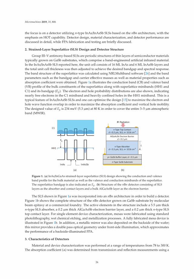
Micromachines 2019, 10, 806
the focus is on a detector utilizing n-type InAs/InAsSb SLSs based on the nBn architecture, with theemphasis on HOT capability. Detector design, material characterization, and detector performance arediscussed in detail, while FPA fabrication and testing are briefly discussed.
2. Strained-Layer Superlattice (SLS) Design and Detector Structure
Group III–V antimony-based SLSs are periodic structures of thin layers of semiconductor materialstypically grown on GaSb substrates, which comprise a band-engineered artificial infrared material.In the InAs/InAsSb SLS reported here, the unit cell consists of 16 ML InAs and 6 ML InAsSb layers andthe total unit cell thickness was then adjusted to achieve the desired bandgap and spectral response.The band structure of the superlattice was calculated using NRLMultiband software [26] and the bandparameters such as the bandgap and carrier effective masses as well as material properties such asabsorption coefficient were obtained. Figure 1a illustrates the conduction band (CB) and valence band(VB) profile of the bulk constituents of the superlattice along with superlattice minibands (HH1 andC1) and its bandgap (Eg). The electron and hole probability distributions are also shown, indicatingnearly free electrons in the C1 miniband and heavily confined holes in the HH1 miniband. This is atypical feature of InAs/InAsSb SLSs and one can optimize the design [15] to maximize the electron andhole wave function overlap in order to maximize the absorption coefficient and vertical hole mobility.The designed value of Eg is 234 meV (5.3 μm) at 80 K in order to cover the entire 3–5 μm atmosphericband (MWIR).
n-Type Top Contact d = 0.2 μm, SLS, n= 1E16 cm-3
AlGaAsSb Electron Barrierd = 0.2 μm
n-Type Absorber d = 5.5 μm, SLS, n= 1E16 cm-3
p+ GaSb Buffer Layer, d = 0.5 μm
n-Type GaSb SubstrateInAs InAsSb
C1
HH1
Eg
(a) (b)
Figure 1. (a) InAs/InGaAs strained-layer superlattice (SLS) design showing the conduction and valenceband profile for the bulk material as well as the valence and conduction minibands of the superlattice.The superlattice bandgap is also indicated as Eg. (b) Structure of the nBn detector consisting of SLSlayers as the absorber and contact layers and a bulk AlGaAsSb layer as the electron barrier.
The SLS shown in Figure 1a was incorporated into an nBn architecture in order to build a detector.Figure 1b shows the complete structure of the nBn detector grown on GaSb substrate by molecularbeam epitaxy at a commercial foundry. The active elements in the structure include a 5.5 μm thickn-type SLS absorber, a 0.2 μm thick AlGaAsSb electron barrier layer, and a 0.2 μm thick n-type SLStop contact layer. For single element device characterization, mesas were fabricated using standardphotolithography, wet chemical etching, and metallization processes. A fully fabricated mesa device isillustrated in Figure 1b. In addition, a metallic mirror was also deposited on the backside of the wafer;this mirror provides a double pass optical geometry under front-side illumination, which approximatesthe performance of a backside-illuminated FPA.
3. Characteristics of Detectors
Material and device characterization was performed at a range of temperatures from 78 to 300 K.The absorption coefficient (α) was determined from transmission and reflection measurements using a
26
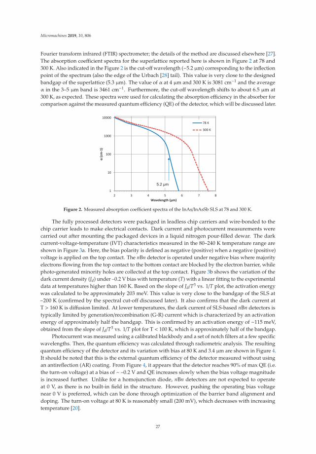
Micromachines 2019, 10, 806
Fourier transform infrared (FTIR) spectrometer; the details of the method are discussed elsewhere [27].The absorption coefficient spectra for the superlattice reported here is shown in Figure 2 at 78 and300 K. Also indicated in the Figure 2 is the cut-offwavelength (~5.2 μm) corresponding to the inflectionpoint of the spectrum (also the edge of the Urbach [28] tail). This value is very close to the designedbandgap of the superlattice (5.3 μm). The value of α at 4 μm and 300 K is 3081 cm−1 and the averageα in the 3–5 μm band is 3461 cm−1. Furthermore, the cut-off wavelength shifts to about 6.5 μm at300 K, as expected. These spectra were used for calculating the absorption efficiency in the absorber forcomparison against the measured quantum efficiency (QE) of the detector, which will be discussed later.
Figure 2. Measured absorption coefficient spectra of the InAs/InAsSb SLS at 78 and 300 K.
The fully processed detectors were packaged in leadless chip carriers and wire-bonded to thechip carrier leads to make electrical contacts. Dark current and photocurrent measurements werecarried out after mounting the packaged devices in a liquid nitrogen pour-filled dewar. The darkcurrent-voltage-temperature (IVT) characteristics measured in the 80–240 K temperature range areshown in Figure 3a. Here, the bias polarity is defined as negative (positive) when a negative (positive)voltage is applied on the top contact. The nBn detector is operated under negative bias where majorityelectrons flowing from the top contact to the bottom contact are blocked by the electron barrier, whilephoto-generated minority holes are collected at the top contact. Figure 3b shows the variation of thedark current density (Jd) under –0.2 V bias with temperature (T) with a linear fitting to the experimentaldata at temperatures higher than 160 K. Based on the slope of Jd/T3 vs. 1/T plot, the activation energywas calculated to be approximately 203 meV. This value is very close to the bandgap of the SLS at~200 K (confirmed by the spectral cut-off discussed later). It also confirms that the dark current atT > 160 K is diffusion limited. At lower temperatures, the dark current of SLS-based nBn detectors istypically limited by generation/recombination (G-R) current which is characterized by an activationenergy of approximately half the bandgap. This is confirmed by an activation energy of ~115 meV,obtained from the slope of Jd/T3 vs. 1/T plot for T < 100 K, which is approximately half of the bandgap.
Photocurrent was measured using a calibrated blackbody and a set of notch filters at a few specificwavelengths. Then, the quantum efficiency was calculated through radiometric analysis. The resultingquantum efficiency of the detector and its variation with bias at 80 K and 3.4 μm are shown in Figure 4.It should be noted that this is the external quantum efficiency of the detector measured without usingan antireflection (AR) coating. From Figure 4, it appears that the detector reaches 90% of max QE (i.e.the turn-on voltage) at a bias of ~ –0.2 V and QE increases slowly when the bias voltage magnitudeis increased further. Unlike for a homojunction diode, nBn detectors are not expected to operateat 0 V, as there is no built-in field in the structure. However, pushing the operating bias voltagenear 0 V is preferred, which can be done through optimization of the barrier band alignment anddoping. The turn-on voltage at 80 K is reasonably small (200 mV), which decreases with increasingtemperature [20].
27
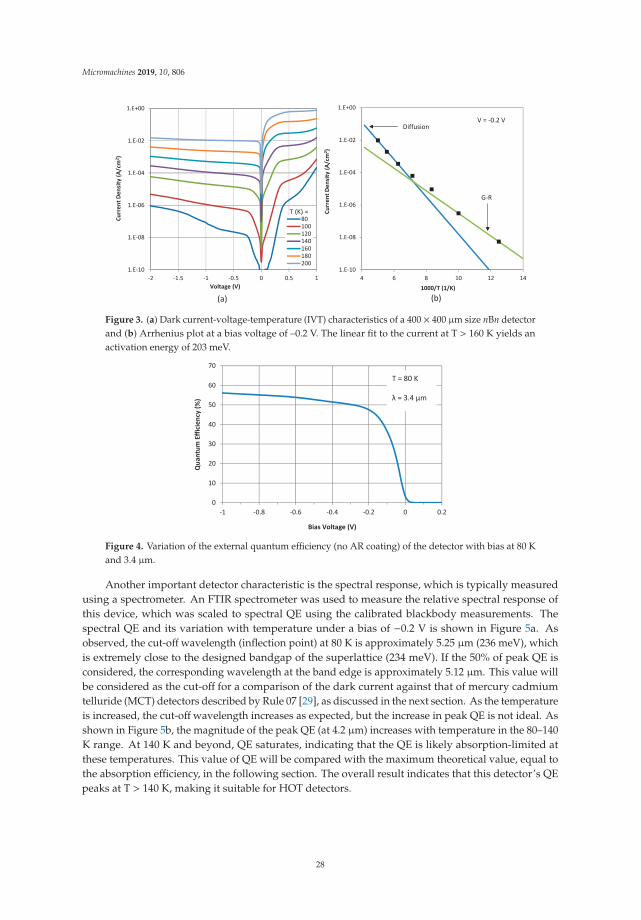
Micromachines 2019, 10, 806
Figure 3. (a) Dark current-voltage-temperature (IVT) characteristics of a 400 × 400 μm size nBn detectorand (b) Arrhenius plot at a bias voltage of –0.2 V. The linear fit to the current at T > 160 K yields anactivation energy of 203 meV.
Figure 4. Variation of the external quantum efficiency (no AR coating) of the detector with bias at 80 Kand 3.4 μm.
Another important detector characteristic is the spectral response, which is typically measuredusing a spectrometer. An FTIR spectrometer was used to measure the relative spectral response ofthis device, which was scaled to spectral QE using the calibrated blackbody measurements. Thespectral QE and its variation with temperature under a bias of −0.2 V is shown in Figure 5a. Asobserved, the cut-off wavelength (inflection point) at 80 K is approximately 5.25 μm (236 meV), whichis extremely close to the designed bandgap of the superlattice (234 meV). If the 50% of peak QE isconsidered, the corresponding wavelength at the band edge is approximately 5.12 μm. This value willbe considered as the cut-off for a comparison of the dark current against that of mercury cadmiumtelluride (MCT) detectors described by Rule 07 [29], as discussed in the next section. As the temperatureis increased, the cut-off wavelength increases as expected, but the increase in peak QE is not ideal. Asshown in Figure 5b, the magnitude of the peak QE (at 4.2 μm) increases with temperature in the 80–140K range. At 140 K and beyond, QE saturates, indicating that the QE is likely absorption-limited atthese temperatures. This value of QE will be compared with the maximum theoretical value, equal tothe absorption efficiency, in the following section. The overall result indicates that this detector’s QEpeaks at T > 140 K, making it suitable for HOT detectors.
28
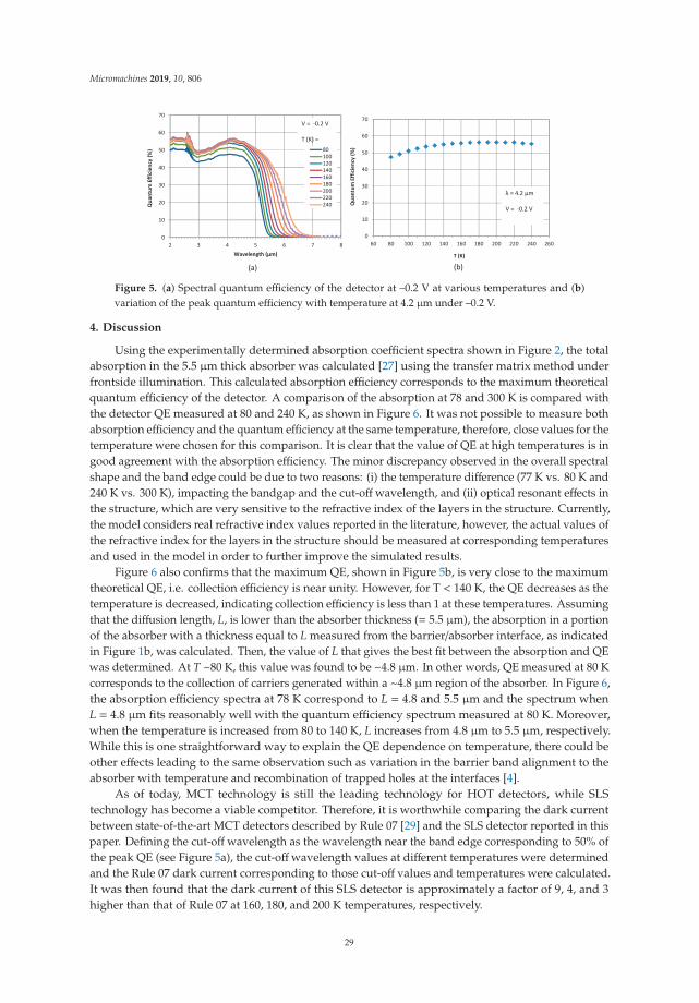
Micromachines 2019, 10, 806
Figure 5. (a) Spectral quantum efficiency of the detector at –0.2 V at various temperatures and (b)variation of the peak quantum efficiency with temperature at 4.2 μm under –0.2 V.
4. Discussion
Using the experimentally determined absorption coefficient spectra shown in Figure 2, the totalabsorption in the 5.5 μm thick absorber was calculated [27] using the transfer matrix method underfrontside illumination. This calculated absorption efficiency corresponds to the maximum theoreticalquantum efficiency of the detector. A comparison of the absorption at 78 and 300 K is compared withthe detector QE measured at 80 and 240 K, as shown in Figure 6. It was not possible to measure bothabsorption efficiency and the quantum efficiency at the same temperature, therefore, close values for thetemperature were chosen for this comparison. It is clear that the value of QE at high temperatures is ingood agreement with the absorption efficiency. The minor discrepancy observed in the overall spectralshape and the band edge could be due to two reasons: (i) the temperature difference (77 K vs. 80 K and240 K vs. 300 K), impacting the bandgap and the cut-off wavelength, and (ii) optical resonant effects inthe structure, which are very sensitive to the refractive index of the layers in the structure. Currently,the model considers real refractive index values reported in the literature, however, the actual values ofthe refractive index for the layers in the structure should be measured at corresponding temperaturesand used in the model in order to further improve the simulated results.
Figure 6 also confirms that the maximum QE, shown in Figure 5b, is very close to the maximumtheoretical QE, i.e. collection efficiency is near unity. However, for T < 140 K, the QE decreases as thetemperature is decreased, indicating collection efficiency is less than 1 at these temperatures. Assumingthat the diffusion length, L, is lower than the absorber thickness (= 5.5 μm), the absorption in a portionof the absorber with a thickness equal to L measured from the barrier/absorber interface, as indicatedin Figure 1b, was calculated. Then, the value of L that gives the best fit between the absorption and QEwas determined. At T ~80 K, this value was found to be ~4.8 μm. In other words, QE measured at 80 Kcorresponds to the collection of carriers generated within a ~4.8 μm region of the absorber. In Figure 6,the absorption efficiency spectra at 78 K correspond to L = 4.8 and 5.5 μm and the spectrum whenL = 4.8 μm fits reasonably well with the quantum efficiency spectrum measured at 80 K. Moreover,when the temperature is increased from 80 to 140 K, L increases from 4.8 μm to 5.5 μm, respectively.While this is one straightforward way to explain the QE dependence on temperature, there could beother effects leading to the same observation such as variation in the barrier band alignment to theabsorber with temperature and recombination of trapped holes at the interfaces [4].
As of today, MCT technology is still the leading technology for HOT detectors, while SLStechnology has become a viable competitor. Therefore, it is worthwhile comparing the dark currentbetween state-of-the-art MCT detectors described by Rule 07 [29] and the SLS detector reported in thispaper. Defining the cut-off wavelength as the wavelength near the band edge corresponding to 50% ofthe peak QE (see Figure 5a), the cut-off wavelength values at different temperatures were determinedand the Rule 07 dark current corresponding to those cut-off values and temperatures were calculated.It was then found that the dark current of this SLS detector is approximately a factor of 9, 4, and 3higher than that of Rule 07 at 160, 180, and 200 K temperatures, respectively.
29
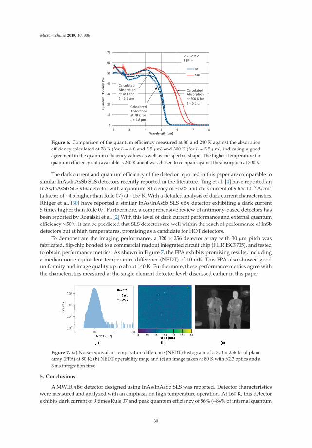
Micromachines 2019, 10, 806
Figure 6. Comparison of the quantum efficiency measured at 80 and 240 K against the absorptionefficiency calculated at 78 K (for L = 4.8 and 5.5 μm) and 300 K (for L = 5.5 μm), indicating a goodagreement in the quantum efficiency values as well as the spectral shape. The highest temperature forquantum efficiency data available is 240 K and it was chosen to compare against the absorption at 300 K.
The dark current and quantum efficiency of the detector reported in this paper are comparable tosimilar InAs/InAsSb SLS detectors recently reported in the literature. Ting et al. [4] have reported anInAs/InAsSb SLS nBn detector with a quantum efficiency of ~52% and dark current of 9.6 × 10⁻⁵ A/cm2
(a factor of ~4.5 higher than Rule 07) at ~157 K. With a detailed analysis of dark current characteristics,Rhiger et al. [30] have reported a similar InAs/InAsSb SLS nBn detector exhibiting a dark current5 times higher than Rule 07. Furthermore, a comprehensive review of antimony-based detectors hasbeen reported by Rogalski et al. [2] With this level of dark current performance and external quantumefficiency >50%, it can be predicted that SLS detectors are well within the reach of performance of InSbdetectors but at high temperatures, promising as a candidate for HOT detectors.
To demonstrate the imaging performance, a 320 × 256 detector array with 30 μm pitch wasfabricated, flip-chip bonded to a commercial readout integrated circuit chip (FLIR ISC9705), and testedto obtain performance metrics. As shown in Figure 7, the FPA exhibits promising results, includinga median noise-equivalent temperature difference (NEDT) of 10 mK. This FPA also showed gooduniformity and image quality up to about 140 K. Furthermore, these performance metrics agree withthe characteristics measured at the single element detector level, discussed earlier in this paper.
Figure 7. (a) Noise-equivalent temperature difference (NEDT) histogram of a 320 × 256 focal planearray (FPA) at 80 K; (b) NEDT operability map; and (c) an image taken at 80 K with f/2.3 optics and a3 ms integration time.
5. Conclusions
A MWIR nBn detector designed using InAs/InAsSb SLS was reported. Detector characteristicswere measured and analyzed with an emphasis on high temperature operation. At 160 K, this detectorexhibits dark current of 9 times Rule 07 and peak quantum efficiency of 56% (~84% of internal quantum
30
Micromachines 2019, 10, 806
efficiency). The turn ON voltage is at or below −200 mV over the full temperature range. It wasestimated that the diffusion length of the SLS is approximately 4.8 μm at 80 K, which increases toa value comparable to the absorber thickness (5.5 μm) when the temperature is increased to 140 K.Comparing the calculated absorption efficiency and the measured detector quantum efficiency, it waspossible to conclude that the detector exhibits nearly 100% collection at temperatures higher than 140 K.While the performance metrics reported here do not meet those of InSb detectors yet, SLS technologycontinues to improve with the promise that it has the potential to deliver future HOT detectors requiredfor many applications.
Author Contributions: Conceptualization, G.A., J.D., C.R. and J.S.; methodology, G.A., J.D., C.R. and J.S.; software,G.A. and J.D.; validation, G.A., J.D., C.R. and J.S.; formal analysis, G.A. and J.D.; investigation, G.A. and J.D.;resources, G.A., J.D., C.R. and J.S.; data curation, G.A. and J.D.; writing—original draft preparation, G.A.;writing—review and editing, J.D., C.R. and J.S.; supervision, C.R. and J.S.; project administration, J.S.; fundingacquisition, J.S.
Funding: This work was funded by the Air Force Research Laboratory, Sensors Directorate under project “III–VFocal Plane Array Development Using Novel Superlattices”.
Acknowledgments: The authors would like to acknowledge the support from the scientists/engineers at theNaval Research Laboratory (NRL) by providing us with the NRL MULTIBANDS software.
Conflicts of Interest: The authors declare no conflict of interest. The funders had no role in the design of thestudy; in the collection, analyses, or interpretation of data; in the writing of the manuscript; or in the decision topublish the results.
References
1. Martyniuk, P.; Rogalski, A. HOT infrared photodetectors. Opto Electron. Rev. 2013, 21, 239–257. [CrossRef]2. Rogalski, A.; Martyniuk, P.; Kopytko, M. Antimonide-Based Infrared Detectors–A New Perspective; SPIE Press:
Bellingham, WA, USA, 2018.3. Pour, S.A.; Huang, E.K.; Chen, G.; Haddadi, A.; Nguyen, B.M.; Razeghi, M. High operating temperature
midwave infrared photodiodes and focal plane arrays based on type-II InAs/GaSb superlattices.Appl. Phys. Lett. 2011, 98, 143501. [CrossRef]
4. Ting, D.Z.; Soibel, A.; Khoshakhlagh, A.; Rafol, S.B.; Keo, S.A.; Höglund, L.; Fisher, A.M.; Luong, E.M.;Gunapala, S.D. Mid-wavelength high operating temperature barrier infrared detector and focal plane array.Appl. Phys. Lett. 2018, 113, 021101. [CrossRef]
5. Maimon, S.; Wicks, G.W. nBn detector, an infrared detector with reduced dark current and higher operatingtemperature. Appl. Phys. Lett. 2006, 89, 151109. [CrossRef]
6. Klem, J.F.; Kim, J.K.; Cich, M.J.; Hawkins, S.D.; Fortune, T.R.; Rienstra, J.L. Comparison of nBn and nBpMid-Wave Barrier Infrared Photodetectors; SPIE Press: Bellingham, WA, USA, 2010; Volume 7608.
7. Plis, E.A.; Krishna, S.S.; Gautam, N.; Myers, S.; Krishna, S. Bias Switchable Dual-Band InAs/GaSb SuperlatticeDetector With pBp Architecture. Photonics J. IEEE 2011, 3, 234–240. [CrossRef]
8. Klipstein, P. “XBn” barrier photodetectors for high sensitivity and high operating temperature infraredsensors. SPIE Proc. 2008, 6940, 69402U.
9. Ting, D.Z.Y.; Hill, C.J.; Soibel, A.; Keo, S.A.; Mumolo, J.M.; Nguyen, J.; Gunapala, S.D. A high-performancelong wavelength superlattice complementary barrier infrared detector. Appl. Phys. Lett. 2009, 95, 023508.[CrossRef]
10. Nolde, J.A.; Jackson, E.M.; Bennett, M.F.; Affouda, C.A.; Cleveland, E.R.; Canedy, C.L.; Vurgaftman, I.;Jernigan, G.G.; Meyer, J.R.; Aifer, E.H. Reticulated shallow etch mesa isolation for controlling surface leakagein GaSb-based infrared detectors. Appl. Phys. Lett. 2017, 111, 051102. [CrossRef]
11. Chang, L.L.; Esaki, L. Electronic properties of InAs-GaSb superlattices. Surf. Sci. 1980, 98, 70–89. [CrossRef]12. Mailhiot, C.; Smith, D.L. Long-wavelength infrared detectors based on strained InAs/Ga1−xInxSb type-II
superlattices. J. Vac. Sci. Technol. A Vac. Surf. Films 1989, 7, 445–449. [CrossRef]13. Nguyen, B.M.; Hoffman, D.; Delaunay, P.Y.; Razeghi, M. Dark current suppression in type II InAs/GaSb
superlattice long wavelength infrared photodiodes with M-structure barrier. Appl. Phys. Lett. 2007, 91,163511–163513. [CrossRef]
31
Micromachines 2019, 10, 806
14. Aifer, E.H.; Tischler, J.G.; Warner, J.H.; Vurgaftman, I.; Bewley, W.W.; Meyer, J.R.; Kim, J.C.; Whitman, L.J.;Canedy, C.L.; Jackson, E.M. W-structured type-II superlattice long-wave infrared photodiodes with highquantum efficiency. Appl. Phys. Lett. 2006, 89, 053519. [CrossRef]
15. Ariyawansa, G.; Reyner, C.J.; Steenbergen, E.H.; Duran, J.M.; Reding, J.D.; Scheihing, J.E.; Bourassa, H.R.;Liang, B.L.; Huffaker, D.L. InGaAs/InAsSb strained layer superlattices for mid-wave infrared detectors.Appl. Phys. Lett. 2016, 108, 022106. [CrossRef]
16. Steenbergen, E.H.; Connelly, B.C.; Metcalfe, G.D.; Shen, H.; Wraback, M.; Lubyshev, D.; Qiu, Y.; Fastenau, J.M.;Liu, A.W.K.; Elhamri, S.; et al. Significantly improved minority carrier lifetime observed in a long-wavelengthinfrared III-V type-II superlattice comprised of InAs/InAsSb. Appl. Phys. Lett. 2011, 99, 251110. [CrossRef]
17. Höglund, L.; Ting, D.Z.; Soibel, A.; Fisher, A.; Khoshakhlagh, A.; Hill, C.J.; Keo, S.; Gunapala, S.D. Minoritycarrier lifetime in mid-wavelength infrared InAs/InAsSb superlattices: Photon recycling and the role ofradiative and Shockley-Read-Hall recombination mechanisms. Appl. Phys. Lett. 2014, 105, 193510. [CrossRef]
18. Kadlec, E.A.; Olson, B.V.; Goldflam, M.D.; Kim, J.K.; Klem, J.F.; Hawkins, S.D.; Coon, W.T.; Cavaliere, M.A.;Tauke-Pedretti, A.; Fortune, T.R.; et al. Effects of electron doping level on minority carrier lifetimes in n-typemid-wave infrared InAs/InAs1-xSbx type-II superlattices. Appl. Phys. Lett. 2016, 109, 261105. [CrossRef]
19. Rogalski, A.; Kopytko, M.; Martyniuk, P. InAs/GaSb type-II superlattice infrared detectors: Three decadesof development. In Infrared Technology and Applications XLIII; SPIE Press: Bellingham, WA, USA, 2017;p. 1017715.
20. Ariyawansa, G.; Reyner, C.J.; Duran, J.M.; Reding, J.D.; Scheihing, J.E.; Steenbergen, E.H. Unipolar infrareddetectors based on InGaAs/InAsSb ternary superlattices. Appl. Phys. Lett. 2016, 109, 021112. [CrossRef]
21. Olson, B.V.; Klem, J.F.; Kadlec, E.A.; Kim, J.K.; Goldflam, M.D.; Hawkins, S.D.; Tauke-Pedretti, A.; Coon, W.T.;Fortune, T.R.; Shaner, E.A.; et al. Vertical Hole Transport and Carrier Localization in InAs/InAsSb Type-IISuperlattice Heterojunction Bipolar Transistors. Phys. Rev. Appl. 2017, 7, 024016. [CrossRef]
22. Rhiger, D.R.; Smith, E.P. Carrier Transport in the Valence Band of nBn III–V Superlattice Infrared Detectors.J. Electron. Mater. 2019, 48, 6053–6062. [CrossRef]
23. Steenbergen, E.H.; Massengale, J.A.; Ariyawansa, G.; Zhang, Y.H. Evidence of carrier localization inphotoluminescence spectroscopy studies of mid-wavelength infrared InAs/InAs1−xSbx type-II superlattices.J. Lumin. 2016, 178, 451–456. [CrossRef]
24. Huang, E.K.; Hoffman, D.; Nguyen, B.; Delaunay, P.; Razeghi, M. Surface leakage reduction in narrow bandgap jour-II antimonide-based superlattice photodiodes. Appl. Phys. Lett. 2009, 94, 053506. [CrossRef]
25. Sidor, D.E.; Savich, G.R.; Wicks, G.W. Surface Leakage Mechanisms in III–V Infrared Barrier Detectors.J. Electron. Mater. 2016, 45, 4663–4667. [CrossRef]
26. Lumb, M.P.; Vurgaftman, I.; Affouda, C.A.; Meyer, J.R.; Aifer, E.H.; Walters, R.J. Quantum wells andsuperlattices for III-V photovoltaics and photodetectors. SPIE Proc. 2012, 8471, 84710A.
27. Ariyawansa, G.; Steenbergen, E.; Bissell, L.J.; Duran, J.M.; Scheihing, J.E.; Eismann, M.T. Absorptioncharacteristics of mid-wave infrared type-II superlattices. SPIE Proc. 2014, 9070, 90701J.
28. Urbach, F. The Long-Wavelength Edge of Photographic Sensitivity and of the Electronic Absorption of Solids.Phys. Rev. 1953, 92, 1324. [CrossRef]
29. Tennant, W.E.; Lee, D.; Zandian, M.; Piquette, E.; Carmody, M. MBE HgCdTe Technology: A Very GeneralSolution to IR Detection, Described by “Rule 07”, a Very Convenient Heuristic. J. Electron. Mater. 2008, 37,1406. [CrossRef]
30. Rhiger, D.R.; Smith, E.P.; Kolasa, B.P.; Kim, J.K.; Klem, J.F.; Hawkins, S.D. Analysis of III–V Superlattice nBnDevice Characteristics. J. Electron. Mater. 2016, 45, 4646–4653. [CrossRef]
© 2019 by the authors. Licensee MDPI, Basel, Switzerland. This article is an open accessarticle distributed under the terms and conditions of the Creative Commons Attribution(CC BY) license (http://creativecommons.org/licenses/by/4.0/).
32
micromachines
Article
Analysis and Simulation of Forcing the Limits ofThermal Sensing for Microbolometers inCMOS–MEMS Technology
Hasan Göktas 1,* and Fikri Serdar Gökhan 2
1 Department of Electrical and Electronic Engineering, Harran University, Sanlıurfa 63000, Turkey2 Department of Electrical and Electronic Engineering, Alanya Alaaddin Keykubat University, Kestel, Alanya,
Antalya 07450, Turkey; [email protected]* Correspondence: [email protected]; Tel.: +90-414-318-3000
Received: 25 September 2019; Accepted: 25 October 2019; Published: 29 October 2019
Abstract: Room-temperature highly sensitive microbolometers are becoming very attractive ininfrared (IR) sensing with the increase in demand for the internet of things (IOT), night vision, andmedical imaging. Different techniques, such as building extremely small-scale devices (nanotubes,etc.) or using 2D materials, showed promising results in terms of high sensitivity with the cost ofchallenges in fabrication and low-noise readout circuit. Here, we propose a new and simple techniqueon the application of joule heating on a clamped–clamped beam without adding any complexity.It provides much better uniformity in temperature distribution in comparison to conventional jouleheating, and this results in higher thermal stresses on fixed ends. This consequently brings around60.5× improvement in the overall temperature sensitivity according to both theory and COMSOL(multiphysics solver). The sensitivity increased with the increase in the stiffness constant, and it wascalculated as 134 N/m for a device with a 60.5× improvement. A considerable amount of decrease inthe operation temperature (36× below 383 K and 47× below 428 K) was achieved via a new technique.That’s why the proposed solution can be used either to build highly reliable long-term devices or toincrease the thermal sensitivity.
Keywords: microbolometer; infrared sensor; complementary metal-oxide semiconductor (CMOS);high sensitivity; temperature sensor; microresonator; MEMS; clamped–clamped beam; thermaldetector
1. Introduction
MEMS/NEMS (Micro/Nano-Electro-Mechanical Systems) resonators got tremendous attention inthe last decades, especially with the increase in the demand for the internet of things (IOT), biosensors,gas sensors, and infrared (IR) sensing applications (night vision, gas detection, medical imaging, etc.).Photon detectors [1,2] and microbolometers [3,4] are the two widely used and well-known competitorsin building IR sensors. Photon detectors suffer from the requirement of cryogenic cooling, intrinsicnoise, relatively high cost, fabrication complexity, and being bulky and expensive. On the otherhand, room-temperature microbolometers not only eliminate all these problems, but can also easilybe implemented in widely used CMOS (complementary metal-oxide semiconductor) processes [3].The working principle of the microbolometer is based on the conversion of incident radiation into heatvia a plasmonic absorber, and then conversion of this heat into an electrical signal via a temperaturesensor. This electrical signal can be either resistance change (non-resonant) or frequency change(resonant type), depending on the device type. Resonant sensors [5–7], in contrast to non-resonantsensors [8], are the most popular because they offer significant advantages [6], such as high-qualityfactor of 1 million [9], ultra-low-noise measurement, and highly accurate measurement. The working
Micromachines 2019, 10, 733; doi:10.3390/mi10110733 www.mdpi.com/journal/micromachines33
Micromachines 2019, 10, 733
principle of MEMS-type resonant-based thermal sensors is based on the resonance frequency shift,with respect to change in the temperature.
Many different techniques have been applied to increase the sensitivity of resonant-typemicrobolometers, where the thermal sensitivity strongly depends on the temperature coefficientof frequency (TCF). Extremely small devices [10,11] have higher sensitivity and a higher TCF, but theyhave challenges, such as difficulties in fabrication, high density integration, and low-noise readoutcircuit implementation. Using NEMS offered better sensitivity and TCF by achieving better thermalisolation [6,12,13], but sacrifices low stiffness constant. High quality factor [9,14,15] was achievedto detect a much smaller frequency shift and consequently enables higher thermal sensitivity anda higher TCF, but this method either requires vacuum environment or fabrication complexity orfabrication compatibility problem with CMOS process. Using phase change materials [16] in buildingcantilever-type resonators increased their thermal sensitivity and TCF, while bringing the fabricationchallenges and CMOS compatibility problem. A fixed–fixed beam-type device was built [17] todrastically increase the TCF in comparison to other well-known resonant-type devices (cantilever,tuning fork, and free-free beam). The |TCF| of 4537 ppm/K was achieved in [5], and 19,500 ppm/K wasachieved in [17], with fixed–fixed beam, where CMOS allowed high density integration and low-noisereadout circuit. Later, this method was improved, and a possibility of 31× improvement, with a |TCF|of 2,178,946 ppm/K in thermal sensing, was demonstrated [7] by not only combining joule heatingwith ambient temperature change but also keeping the pull-in voltage as small as possible. However,nonuniform temperature distribution via joule heating prevented this approach from going down tosmaller scale and consequently having higher thermal sensitivity due to relatively high thermal stresses.
We present a new type of joule heating technique in this work that allows much better temperatureuniformity throughout the beam in comparison to conventional joule heating. In contrast to [7], here,joule heating is applied on sidebars attached on the fixed ends of the clamped–clamped beam. Thisuniform temperature profile not only increases the thermal stress on the fixed ends but also allowsbuilding design with relatively higher stiffness constant, while keeping the temperature limit around530 K [18]. This increase in return results in the increase in the sensitivity multiplier and TCF. Thesensitivity multiplier was computed as 60.5×, with a 30 μm long and 0.9 μm thick device, accordingto both COMSOL and theory in comparison to the possibility of 31× demonstrated in [7]. The |TCF|for 60.8× improvement was calculated as 3,991,168 ppm/K in comparison to 2,178,946 ppm/K in [7],19,500 ppm/K in [17], 4537 ppm/K in [5], 30 ppm/K in [6], 548 ppm/K in [10], 86.2 ppm/K in [19], and29.4 ppm/K in [13]. Furthermore, this uniform heating allows the design to have the same thermalsensitivity, with a conventional joule heating scheme [7], while drastically decreasing the operationtemperature and enabling long-term operation. In other words, the proposed design methodologycan be used either to increase the thermal sensitivity or to decrease the operation temperature forhigh reliability.
Using aluminum or composite structure in building a clamped–clamped beam in a CMOS0.6 process showed almost no difference in the sensitivity multiplier, even at different sizes, wherethe stiffness constant stayed the same. That’s why optimum design with a critical temperature below530 K can be designed in any fabrication process/technology (CMOS, silicon, Silicon on insulator (SOI),etc.), regardless of the material and size, as long as the stiffness constant is limited to 134 N/m.
2. Theory, Design, and Optimization
The main mechanism behind the wide-range frequency tuning is the thermal stresses createdvia joule heating, as demonstrated for the first time in [17]. Another study [7] conducted on CMOSclamped–clamped beam proved that thermal stress is the dominant factor on the temperature sensitivity,and the stresses caused by the increase in the pull-in force adversely affect the sensitivity. The maingoal of this study is to increase the temperature uniformity throughout the beam to get further increasein the thermal stress at a relatively low temperature, and consequently get higher thermal sensitivityfor microbolometer applications.
34
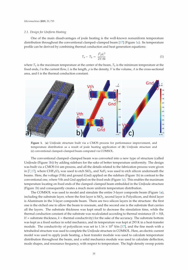
Micromachines 2019, 10, 733
2.1. Design for Uniform Heating
One of the main disadvantages of joule heating is the well-known nonuniform temperaturedistribution throughout the conventional clamped–clamped beam [17] (Figure 1c). Its temperatureprofile can be derived by combining thermal conduction and heat generation equations:
Ta − Tb =I2ρL3
2VAk(1)
where Ta is the maximum temperature at the center of the beam, Tb is the minimum temperature at thefixed ends, I is the current flow, L is the length, ρ is the density, V is the volume, A is the cross-sectionalarea, and k is the thermal conduction constant.
Figure 1. (a) UniJoule structure built via a CMOS process for performance improvement, andtemperature distribution as a result of joule heating application of (b) UniJoule structure and(c) conventional clamped–clamped beam computed via COMSOL.
The conventional clamped–clamped beam was converted into a new type of structure (calledUniJoule (Figure 1b)) by adding sidebars for the sake of better temperature uniformity. The designwas built via a CMOS 0.6 um process, and all the details related to the fabrication process were givenin [7,17], where CHF3/O2 was used to etch SiO2, and XeF2 was used to etch silicon underneath thebeams. Here, the voltage (Vth) and ground (Gnd) applied on the sidebars (Figure 1b) in contrast to theconventional one, where Vth and Gnd applied on the fixed ends (Figure 1c). This enables the maximumtemperature locating on fixed ends of the clamped–clamped beam embedded in the UniJoule structure(Figure 1b) and consequently creates a much more uniform temperature distribution.
The COMSOL was used to model and simulate the entire 3-layer composite beam (Figure 1a),including the substrate layer, where the first layer is SiO2, second layer is Polysilicon, and third layeris Aluminum in the 3-layer composite beam. There are two silicon layers in the structure: the firstone is the etched one to allow the beam to resonate, and the second one is the substrate that carriesall the layers. The substrate thickness was kept small to decrease the simulation time, while thethermal conduction constant of the substrate was recalculated according to thermal resistance (R = H/k,H = substrate thickness, k = thermal conductivity) for the sake of the accuracy. The substrate bottomwas kept as a fixed surface in solid mechanics, and its temperature was kept at 293 K in a heat-transfermodule. The conductivity of polysilicon was set to 1.16 × 10⁵ S/m [17], and the fine mesh with atetrahedral structure was used to complete the UniJoule structure in COMSOL. Here, an electric currentmodel was used to apply joule heating, a heat transfer module was used to calculate temperaturedistribution throughout the beam, and a solid mechanics module was used to calculate deflection,mode shapes, and resonance frequency, with respect to temperature. The high-density sweep points
35
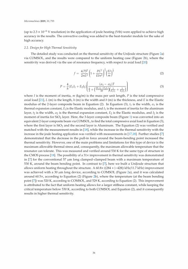
Micromachines 2019, 10, 733
(up to 2.3 × 10⁻⁶ V resolution) in the application of joule heating (Vth) were applied to achieve highaccuracy in the results. The convective cooling was added to the heat-transfer module for the sake ofhigh accuracy.
2.2. Design for High Thermal Sensitivity
The detailed study was conducted on the thermal sensitivity of the UniJoule structure (Figure 2a)via COMSOL, and the results were compared to the uniform heating case (Figure 2b), where thesensitivity was derived via the use of resonance frequency, with respect to axial load [20]:
f =4.732
2πL2
(1 +
PL2
EIπ2
) 12 (EI
m
) 12
(2)
P =4h(E1I1 + E2I2)
⎛⎜⎜⎜⎜⎜⎜⎝(α1 − α2)T
h2 +( 2E1I1+E2I2
hb
)(1
E1t1+ 1
E2t2
)⎞⎟⎟⎟⎟⎟⎟⎠ (3)
where I is the moment of inertia, m (kg/m) is the mass per unit length, P is the total compressiveaxial load [21], L (m) is the length, h (m) is the width and b (m) is the thickness, and E is the Elasticmodulus of the 2-layer composite beam in Equation (2). In Equation (3), t1 is the width, α1 is thethermal expansion constant, E1is the Elastic modulus, and I1 is the moment of inertia for the aluminumlayer, t2 is the width, α2 is the thermal expansion constant, E2 is the Elastic modulus, and I2 is themoment of inertia for SiO2 layer. Here, the 3-layer composite beam (Figure 1) was converted into anequivalent 2-layer composite beam via COMSOL, to find the total compressive axial load in Equation (3),where the first layer is SiO2 and the second layer is Aluminum. The Equation (2) was verified andmatched with the measurement results in [18], while the increase in the thermal sensitivity with theincrease in the joule heating application was verified with measurements in [17,18]. Further studies [7]demonstrated that the decrease in the pull-in force around the beam-bending point increased thethermal sensitivity. However, one of the main problems and limitations for this type of device is themaximum allowable thermal stress and, consequently, the maximum allowable temperature that theresonator can tolerate. This was measured and verified around 530 K for the same type of structure inthe CMOS process [18]. The possibility of a 31× improvement in thermal sensitivity was demonstratedin [7] for the conventional 57 μm long clamped–clamped beam with a maximum temperature of530 K, around the beam bending point. In contrast to [7], here we built a UniJoule structure thatallows uniform heating throughout the structure. A 60.8× ((284 + |−428|) kHz/11.7 kHz) improvementwas achieved with a 30 μm long device, according to COMSOL (Figure 2a), and it was calculatedaround 60.5×, according to Equation (2) (Figure 2b), where the temperature (at the beam bendingpoint [7]) was 520 K, according to COMSOL, and 529 K, according to Equation (2). This improvementis attributed to the fact that uniform heating allows for a larger stiffness constant, while keeping thecritical temperature below 530 K, according to both COMSOL and Equation (2), and it consequentlyresults in higher thermal sensitivity.
36
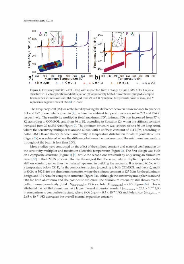
Micromachines 2019, 10, 733
Figure 2. Frequency shift (FS = Fr1 − Fr2) with respect to 1 Kelvin change by (a) COMSOL for UniJoulestructure with Vth application and (b) Equation (2) for uniformly heated conventional clamped–clampedbeam, when stiffness constant (K) changed from 29 to 338 N/m; here, X represents positive max, and Yrepresents negative max of FS [22] in inset.
The Frequency shift (FS) was calculated by taking the difference between two resonance frequenciesFr1 and Fr2 (more details given in [7]), where the ambient temperatures were set as 293 and 294 K,respectively. The sensitivity multiplier (total maximum FS/minimum FS) was increased from 37 to82, according to COMSOL, and from 36 to 82, according to Equation (2), when the stiffness constantincreased from 29 to 338 N/m (Figure 2). The optimum structure was selected to be a 30 μm long beam,where the sensitivity multiplier is around 60.5×, with a stiffness constant of 134 N/m, according toboth COMSOL and theory. A decent uniformity in temperature distribution for all UniJoule structures(Figure 2a) was achieved where the difference between the maximum and the minimum temperaturethroughout the beam is less than 6.5%.
More studies were conducted on the effect of the stiffness constant and material configuration onthe sensitivity multiplier and maximum allowable temperature (Figure 3). The first design was builton a composite structure (Figure 1) [5], while the second one was built by only using an aluminumlayer [22] in the CMOS process. The results suggest that the sensitivity multiplier depends on thestiffness constant, rather than the material type used in building the resonator. It is around 60.5×, witha temperature below 530 K, for the composite structure (according to both COMSOL and theory), and itis 60.2× at 502 K for the aluminum resonator, where the stiffness constant is 127 N/m for the aluminumdesign and 134 N/m for composite structure (Figure 3a). Although the sensitivity multiplier is around60× for both aluminum and the composite structure, the aluminum resonator still shows overallbetter thermal sensitivity (total |FSaluminum| = 1306 vs. total |FScomposite| = 712) (Figure 3a). This isattributed the fact that aluminum has a larger thermal expansion constant (αAluminum = 23.1 × 10⁻⁶ 1/K)in comparison to composite structure, where SiO2 (αSiO2 = 0.5 × 10⁻⁶ 1/K) and Polysilicon (αPolysilicon =
2.65 × 10⁻⁶ 1/K) decreases the overall thermal expansion constant.
37
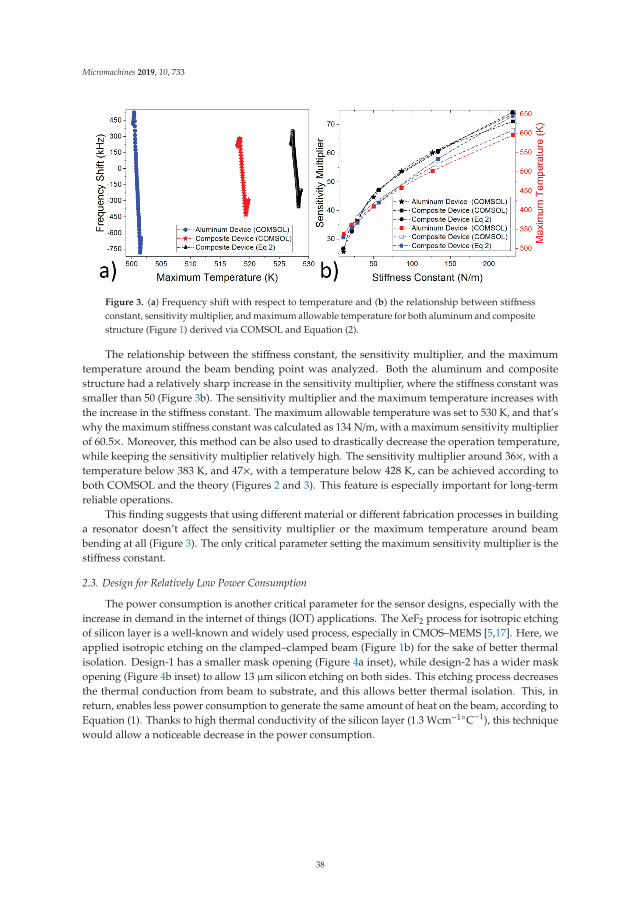
Micromachines 2019, 10, 733
Figure 3. (a) Frequency shift with respect to temperature and (b) the relationship between stiffnessconstant, sensitivity multiplier, and maximum allowable temperature for both aluminum and compositestructure (Figure 1) derived via COMSOL and Equation (2).
The relationship between the stiffness constant, the sensitivity multiplier, and the maximumtemperature around the beam bending point was analyzed. Both the aluminum and compositestructure had a relatively sharp increase in the sensitivity multiplier, where the stiffness constant wassmaller than 50 (Figure 3b). The sensitivity multiplier and the maximum temperature increases withthe increase in the stiffness constant. The maximum allowable temperature was set to 530 K, and that’swhy the maximum stiffness constant was calculated as 134 N/m, with a maximum sensitivity multiplierof 60.5×. Moreover, this method can be also used to drastically decrease the operation temperature,while keeping the sensitivity multiplier relatively high. The sensitivity multiplier around 36×, with atemperature below 383 K, and 47×, with a temperature below 428 K, can be achieved according toboth COMSOL and the theory (Figures 2 and 3). This feature is especially important for long-termreliable operations.
This finding suggests that using different material or different fabrication processes in buildinga resonator doesn’t affect the sensitivity multiplier or the maximum temperature around beambending at all (Figure 3). The only critical parameter setting the maximum sensitivity multiplier is thestiffness constant.
2.3. Design for Relatively Low Power Consumption
The power consumption is another critical parameter for the sensor designs, especially with theincrease in demand in the internet of things (IOT) applications. The XeF2 process for isotropic etchingof silicon layer is a well-known and widely used process, especially in CMOS–MEMS [5,17]. Here, weapplied isotropic etching on the clamped–clamped beam (Figure 1b) for the sake of better thermalisolation. Design-1 has a smaller mask opening (Figure 4a inset), while design-2 has a wider maskopening (Figure 4b inset) to allow 13 μm silicon etching on both sides. This etching process decreasesthe thermal conduction from beam to substrate, and this allows better thermal isolation. This, inreturn, enables less power consumption to generate the same amount of heat on the beam, according toEquation (1). Thanks to high thermal conductivity of the silicon layer (1.3 Wcm−1◦C−1), this techniquewould allow a noticeable decrease in the power consumption.
38
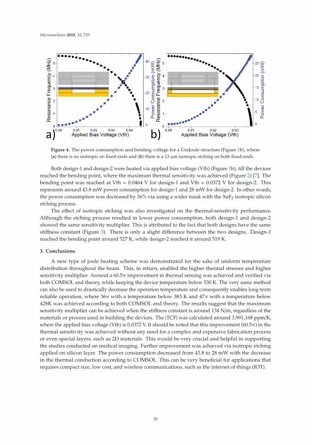
Micromachines 2019, 10, 733
Figure 4. The power consumption and bending voltage for a UniJoule structure (Figure 1b), where(a) there is no isotropic on fixed-ends and (b) there is a 13 μm isotropic etching on both fixed-ends.
Both design-1 and design-2 were heated via applied bias voltage (Vth) (Figure 1b), till the devicesreached the bending point, where the maximum thermal sensitivity was achieved (Figure 2) [7]. Thebending point was reached at Vth = 0.0464 V for design-1 and Vth = 0.0372 V for design-2. Thisrepresents around 43.8 mW power consumption for design-1 and 28 mW for design-2. In other words,the power consumption was decreased by 36% via using a wider mask with the XeF2 isotropic siliconetching process.
The effect of isotropic etching was also investigated on the thermal-sensitivity performance.Although the etching process resulted in lower power consumption, both design-1 and design-2showed the same sensitivity multiplier. This is attributed to the fact that both designs have the samestiffness constant (Figure 3). There is only a slight difference between the two designs. Design-1reached the bending point around 527 K, while design-2 reached it around 519 K.
3. Conclusions
A new type of joule heating scheme was demonstrated for the sake of uniform temperaturedistribution throughout the beam. This, in return, enabled the higher thermal stresses and highersensitivity multiplier. Around a 60.5× improvement in thermal sensing was achieved and verified viaboth COMSOL and theory, while keeping the device temperature below 530 K. The very same methodcan also be used to drastically decrease the operation temperature and consequently enables long-termreliable operation, where 36× with a temperature below 383 K and 47× with a temperature below428K was achieved according to both COMSOL and theory. The results suggest that the maximumsensitivity multiplier can be achieved when the stiffness constant is around 134 N/m, regardless of thematerials or process used in building the devices. The |TCF| was calculated around 3,991,168 ppm/K,where the applied bias voltage (Vth) is 0.0372 V. It should be noted that this improvement (60.5×) in thethermal sensitivity was achieved without any need for a complex and expensive fabrication processor even special layers, such as 2D materials. This would be very crucial and helpful in supportingthe studies conducted on medical imaging. Further improvement was achieved via isotropic etchingapplied on silicon layer. The power consumption decreased from 43.8 to 28 mW with the decreasein the thermal conduction according to COMSOL. This can be very beneficial for applications thatrequires compact size, low cost, and wireless communications, such as the internet of things (IOT).
39
Micromachines 2019, 10, 733
Author Contributions: Conceptualization, H.G.; Methodology, H.G.; Software, H.G. and F.S.G.; Validation, H.G.and F.S.G.; Formal Analysis, H.G.; Investigation, H.G. and F.S.G.; Resources, H.G. and F.S.G.; Data Curation, H.G.and F.S.G.; Writing-Original Draft Preparation, H.G.; Writing-Review & Editing, H.G. and F.S.G.; Visualization,H.G. and F.S.G.; Supervision, H.G.; Project Administration, H.G.; Funding Acquisition, H.G.
Funding: This research was funded by the Scientific Research Project Foundation of Turkey (grant number 18073).
Acknowledgments: The author especially wishes to thank COMSOL for their support in setting up the simulationenvironment accurately for CMOS–MEMS resonator in this study.
Conflicts of Interest: The authors declare no conflicts of interest.
References
1. Marsili, F.; Verma, V.B.; Stern, J.A.; Harrington, S.; Lita, A.E.; Gerrits, T.; Vayshenker, I.; Baek, B.; Shaw, M.D.;Mirin, R.P.; et al. Detecting single infrared photons with 93% system efficiency. Nat. Photonics 2013, 7, 210–214.[CrossRef]
2. Renema, J.J.; Gaudio, R.; Wang, Q.; Zhou, Z.; Gaggero, A.; Mattioli, F.; Leoni, R.; Sahin, D.; de Dood, M.J.A.;Fiore, A.; et al. Experimental Test of Theories of the Detection Mechanism in a Nanowire SuperconductingSingle Photon Detector. Phys. Rev. Lett. 2014, 112, 117604. [CrossRef] [PubMed]
3. Forsberg, F.; Lapadatu, A.; Kittilsland, G.; Martinsen, S.; Roxhed, N.; Fischer, A.C.; Stemme, G.; Samel, B.;Ericsson, P.; Høivik, N.; et al. CMOS-Integrated Si/SiGe Quantum-Well Infrared Microbolometer FocalPlane Arrays Manufactured With Very Large-Scale Heterogeneous 3-D Integration. IEEE J. Sel. Top.Quantum Electron. 2015, 21, 30–40. [CrossRef]
4. Lv, J.; Que, L.; Wei, L.; Zhou, Y.; Liao, B.; Jiang, Y. Uncooled Microbolometer Infrared Focal Plane ArrayWithout Substrate Temperature Stabilization. IEEE Sens. J. 2014, 14, 1533–1544. [CrossRef]
5. Göktas, H.; Turner, K.L.; Zaghloul, M.E. Enhancement in CMOS-MEMS Resonator for High SensitiveTemperature Sensing. IEEE Sens. J. 2017, 17, 598–603. [CrossRef]
6. Hui, Y.; Gomez-Diaz, J.S.; Qian, Z.; Alù, A.; Rinaldi, M. Plasmonic piezoelectric nanomechanical resonatorfor spectrally selective infrared sensing. Nat. Commun. 2016, 7, 11249. [CrossRef]
7. Göktas, H. Towards an Ultra-Sensitive Temperature Sensor for Uncooled Infrared Sensing in CMOS–MEMSTechnology. Micromachines 2019, 10, 108. [CrossRef] [PubMed]
8. Kang, D.H.; Kim, K.W.; Lee, S.Y.; Kim, Y.H.; Keun Gil, S. Influencing factors on the pyroelectric properties ofPb (Zr, Ti) O3 thin film for uncooled infrared detector. Mater. Chem. Phys. 2005, 90, 411–416. [CrossRef]
9. Tao, Y.; Boss, J.M.; Moores, B.A.; Degen, C.L. Single-crystal diamond nanomechanical resonators with qualityfactors exceeding one million. Nat. Commun. 2014, 5, 3638. [CrossRef]
10. Zhang, X.C.; Myers, E.B.; Sader, J.E.; Roukes, M.L. Nanomechanical Torsional Resonators for Frequency-ShiftInfrared Thermal Sensing. ACS Nano Lett. 2013, 13, 1528–1534. [CrossRef] [PubMed]
11. Sawano, S.; Arie, T.; Akita, S. Carbon Nanotube Resonator in Liquid. ACS Nano Lett. 2010, 10, 3395–3398.[CrossRef] [PubMed]
12. Baek, I.-B.; Byun, S.; Lee, B.K.; Ryu, J.-H.; Kim, Y.; Yoon, Y.S.; Jang, W.I.; Lee, S.; Yu, H.Y. Attogram masssensing based on silicon microbeam resonators. Nat. Sci. Rep. 2017, 7, 46660. [CrossRef] [PubMed]
13. Qian, Z.; Hui, Y.; Liu, F.; Kang, S.; Kar, S.; Rinaldi, M. Graphene–aluminum nitride NEMS resonant infrareddetector. Nat. Microsyst. Nanoeng. 2016, 2, 16026. [CrossRef] [PubMed]
14. Foulgoc, B.L.; Bourouina, T.; Traon, O.L.; Bosseboeuf, A.; Marty, F.; Breluzeau, C.; Grandchamp, J.-P.;Masson, S. Highly decoupled single-crystal silicon resonators: An approach for the intrinsic quality factor.IOP J. Micromech. Microeng. 2006, 16, S45–S53. [CrossRef]
15. Laird, E.A.; Pei, F.; Tang, W.; Steele, G.A.; Kouwenhoven, L.P. A High Quality Factor Carbon NanotubeMechanical Resonator at 39 GHz. ACS Nano Lett. 2012, 12, 193–197. [CrossRef] [PubMed]
16. Manca, N.; Pellegrino, L.; Kanki, T.; Yamasaki, S.; Tanaka, H.; Siri, A.S.; Marré, D. Programmable MechanicalResonances in MEMS by Localized Joule Heating of Phase Change Materials. Adv. Mater. 2013, 25, 6430–6435.[CrossRef] [PubMed]
17. Göktas, H.; Zaghloul, M.E. Tuning In-Plane Fixed–Fixed Beam Resonators with Embedded Heater in CMOSTechnology. IEEE Electron Device Lett. 2015, 36, 189–191. [CrossRef]
18. Göktas, H.; Zaghloul, M.E. The implementation of low-power and wide tuning range MEMS filters forcommunication applications. Radio Sci. 2016, 51, 1636–1644. [CrossRef]
40
Micromachines 2019, 10, 733
19. Duraffourg, L.; Laurent, L.; Moulet, J.-S.; Arcamone, J.; Yon, J.-J. Array of Resonant ElectromechanicalNanosystems: A Technological Breakthrough for Uncooled Infrared Imaging. Micromachines 2018, 10, 401.[CrossRef] [PubMed]
20. Jha, C.M. Thermal and Mechanical Isolation of Ovenized MEMS Resonator. Ph.D. Thesis, Department ofMechanical Engineering, Stanford University, Palo Alto, CA, USA, 2008.
21. Abawi, A.T. The Bending of Bonded Layers Due to Thermal Stress. Available online: http://hlsresearch.com/personnel/abawi/papers/bend.pdf (accessed on 23 October 2014).
22. Verd, J.; Uranga, A.; Abadal, G.; Teva, J.; Torres, F.; Pérez-Murano, F.; Fraxedas, J.; Esteve, J.; Barniol, N.Monolithic mass sensor fabricated using a conventional technology with attogram resolution in air conditions.Appl. Phys. Lett. 2007, 91, 013501. [CrossRef]
© 2019 by the authors. Licensee MDPI, Basel, Switzerland. This article is an open accessarticle distributed under the terms and conditions of the Creative Commons Attribution(CC BY) license (http://creativecommons.org/licenses/by/4.0/).
41

micromachines
Review
InAs/InAsSb Type-II Strained-Layer SuperlatticeInfrared Photodetectors
David Z. Ting *, Sir B. Rafol, Arezou Khoshakhlagh, Alexander Soibel, Sam A. Keo,
Anita M. Fisher, Brian J. Pepper, Cory J. Hill and Sarath D. Gunapala
NASA Jet Propulsion Laboratory, California Institute of Technology, Pasadena, CA 91109, USA;[email protected] (S.B.R.); [email protected] (A.K.);[email protected] (A.S.); [email protected] (S.A.K.); [email protected] (A.M.F.);[email protected] (B.J.P.); [email protected] (C.J.H.); [email protected] (S.D.G.)* Correspondence: [email protected]
Received: 22 September 2020; Accepted: 21 October 2020; Published: 26 October 2020
Abstract: The InAs/InAsSb (Gallium-free) type-II strained-layer superlattice (T2SLS) has emerged inthe last decade as a viable infrared detector material with a continuously adjustable band gap capable ofaccommodating detector cutoffwavelengths ranging from 4 to 15 μm and beyond. When coupled withthe unipolar barrier infrared detector architecture, the InAs/InAsSb T2SLS mid-wavelength infrared(MWIR) focal plane array (FPA) has demonstrated a significantly higher operating temperature thanInSb FPA, a major incumbent technology. In this brief review paper, we describe the emergence of theInAs/InAsSb T2SLS infrared photodetector technology, point out its advantages and disadvantages,and survey its recent development.
Keywords: InAs/InAsSb; type-II superlattice; infrared detector; mid-wavelength infrared (MWIR);unipolar barrier
1. Introduction
The II-VI semiconductor HgCdTe (MCT) is the most successful infrared photodetector materialto date. MCT grown on nearly lattice-matched CdZnTe (CZT) substrate offers continuous cutoffwavelength (λcutoff) coverage from the short-wave infrared (SWIR) to the very long wavelength infrared(VLWIR), while providing a high quantum efficiency (QE) and low dark current for high-performanceapplications. In general, III-V semiconductors are more robust than their II-VI counterparts due to theirstronger, less ionic chemical bonding. III-V semiconductor-based infrared focal plane arrays (FPAs)excel in operability, spatial uniformity, temporal stability, scalability, producibility, and affordability.InGaAs FPAs with λcutoff ~ 1.7 μm perform at near theoretical limit and dominate the SWIR FPAmarket. InSb FPAs (λcutoff ~ 5.3 μm), despite a significantly lower operating temperature than MCT,lead the mid-wavelength infrared (MWIR) market in volume due to their superior manufacturabilityand lower cost. The major limitation for traditional bulk III-V semiconductor detectors grown on(nearly) lattice-matched substrates is the lack of pervasive cutoffwavelength adjustability.
1.1. Advances in III-V Infrared Material
One method to achieve a wide-range cutoff wavelength adjustability in III-V semiconductors is touse bulk InAsSb alloy grown on metamorphic buffers. Recent results show that the InAsSb band gapbowing is significantly larger than previously believed, and up to λcutoff ~ 12.4 μm could be achieved [1].In addition, nearly lattice-matched or pseudomorphic III-V semiconductor type-II superlattices (T2SLs)can provide a high degree of flexibility in cutoff wavelength. They can have a sufficient absorptionstrength to attain ample quantum efficiency, are less susceptible to band-to-band tunneling than bulk
Micromachines 2020, 11, 958; doi:10.3390/mi11110958 www.mdpi.com/journal/micromachines43
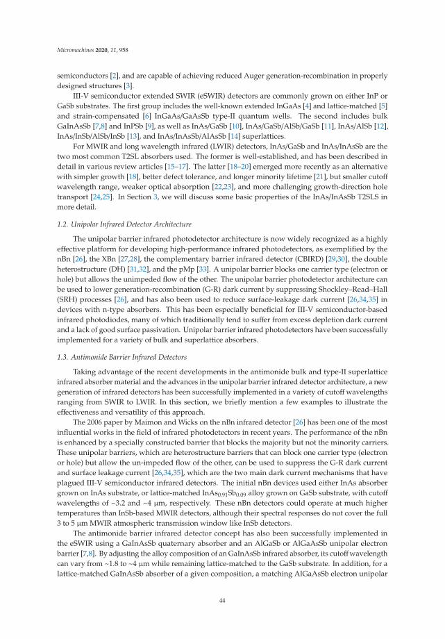
Micromachines 2020, 11, 958
semiconductors [2], and are capable of achieving reduced Auger generation-recombination in properlydesigned structures [3].
III-V semiconductor extended SWIR (eSWIR) detectors are commonly grown on either InP orGaSb substrates. The first group includes the well-known extended InGaAs [4] and lattice-matched [5]and strain-compensated [6] InGaAs/GaAsSb type-II quantum wells. The second includes bulkGaInAsSb [7,8] and InPSb [9], as well as InAs/GaSb [10], InAs/GaSb/AlSb/GaSb [11], InAs/AlSb [12],InAs/InSb/AlSb/InSb [13], and InAs/InAsSb/AlAsSb [14] superlattices.
For MWIR and long wavelength infrared (LWIR) detectors, InAs/GaSb and InAs/InAsSb are thetwo most common T2SL absorbers used. The former is well-established, and has been described indetail in various review articles [15–17]. The latter [18–20] emerged more recently as an alternativewith simpler growth [18], better defect tolerance, and longer minority lifetime [21], but smaller cutoffwavelength range, weaker optical absorption [22,23], and more challenging growth-direction holetransport [24,25]. In Section 3, we will discuss some basic properties of the InAs/InAsSb T2SLS inmore detail.
1.2. Unipolar Infrared Detector Architecture
The unipolar barrier infrared photodetector architecture is now widely recognized as a highlyeffective platform for developing high-performance infrared photodetectors, as exemplified by thenBn [26], the XBn [27,28], the complementary barrier infrared detector (CBIRD) [29,30], the doubleheterostructure (DH) [31,32], and the pMp [33]. A unipolar barrier blocks one carrier type (electron orhole) but allows the unimpeded flow of the other. The unipolar barrier photodetector architecture canbe used to lower generation-recombination (G-R) dark current by suppressing Shockley–Read–Hall(SRH) processes [26], and has also been used to reduce surface-leakage dark current [26,34,35] indevices with n-type absorbers. This has been especially beneficial for III-V semiconductor-basedinfrared photodiodes, many of which traditionally tend to suffer from excess depletion dark currentand a lack of good surface passivation. Unipolar barrier infrared photodetectors have been successfullyimplemented for a variety of bulk and superlattice absorbers.
1.3. Antimonide Barrier Infrared Detectors
Taking advantage of the recent developments in the antimonide bulk and type-II superlatticeinfrared absorber material and the advances in the unipolar barrier infrared detector architecture, a newgeneration of infrared detectors has been successfully implemented in a variety of cutoff wavelengthsranging from SWIR to LWIR. In this section, we briefly mention a few examples to illustrate theeffectiveness and versatility of this approach.
The 2006 paper by Maimon and Wicks on the nBn infrared detector [26] has been one of the mostinfluential works in the field of infrared photodetectors in recent years. The performance of the nBnis enhanced by a specially constructed barrier that blocks the majority but not the minority carriers.These unipolar barriers, which are heterostructure barriers that can block one carrier type (electronor hole) but allow the un-impeded flow of the other, can be used to suppress the G-R dark currentand surface leakage current [26,34,35], which are the two main dark current mechanisms that haveplagued III-V semiconductor infrared detectors. The initial nBn devices used either InAs absorbergrown on InAs substrate, or lattice-matched InAs0.91Sb0.09 alloy grown on GaSb substrate, with cutoffwavelengths of ~3.2 and ~4 μm, respectively. These nBn detectors could operate at much highertemperatures than InSb-based MWIR detectors, although their spectral responses do not cover the full3 to 5 μm MWIR atmospheric transmission window like InSb detectors.
The antimonide barrier infrared detector concept has also been successfully implemented inthe eSWIR using a GaInAsSb quaternary absorber and an AlGaSb or AlGaAsSb unipolar electronbarrier [7,8]. By adjusting the alloy composition of an GaInAsSb infrared absorber, its cutoffwavelengthcan vary from ~1.8 to ~4 μm while remaining lattice-matched to the GaSb substrate. In addition, for alattice-matched GaInAsSb absorber of a given composition, a matching AlGaAsSb electron unipolar
44
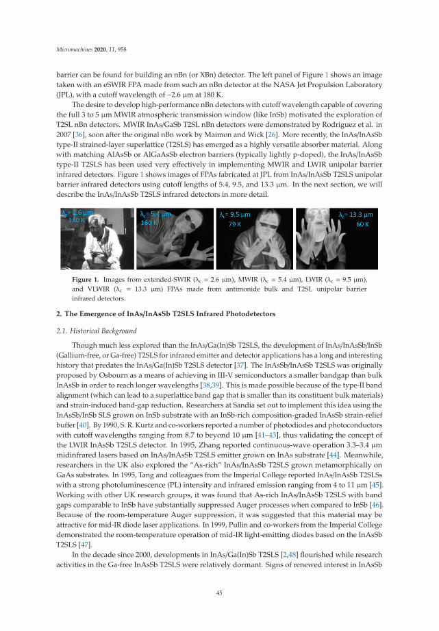
Micromachines 2020, 11, 958
barrier can be found for building an nBn (or XBn) detector. The left panel of Figure 1 shows an imagetaken with an eSWIR FPA made from such an nBn detector at the NASA Jet Propulsion Laboratory(JPL), with a cutoffwavelength of ~2.6 μm at 180 K.
The desire to develop high-performance nBn detectors with cutoffwavelength capable of coveringthe full 3 to 5 μm MWIR atmospheric transmission window (like InSb) motivated the exploration ofT2SL nBn detectors. MWIR InAs/GaSb T2SL nBn detectors were demonstrated by Rodriguez et al. in2007 [36], soon after the original nBn work by Maimon and Wick [26]. More recently, the InAs/InAsSbtype-II strained-layer superlattice (T2SLS) has emerged as a highly versatile absorber material. Alongwith matching AlAsSb or AlGaAsSb electron barriers (typically lightly p-doped), the InAs/InAsSbtype-II T2SLS has been used very effectively in implementing MWIR and LWIR unipolar barrierinfrared detectors. Figure 1 shows images of FPAs fabricated at JPL from InAs/InAsSb T2SLS unipolarbarrier infrared detectors using cutoff lengths of 5.4, 9.5, and 13.3 μm. In the next section, we willdescribe the InAs/InAsSb T2SLS infrared detectors in more detail.
Figure 1. Images from extended-SWIR (λc = 2.6 μm), MWIR (λc = 5.4 μm), LWIR (λc = 9.5 μm),and VLWIR (λc = 13.3 μm) FPAs made from antimonide bulk and T2SL unipolar barrierinfrared detectors.
2. The Emergence of InAs/InAsSb T2SLS Infrared Photodetectors
2.1. Historical Background
Though much less explored than the InAs/Ga(In)Sb T2SLS, the development of InAs/InAsSb/InSb(Gallium-free, or Ga-free) T2SLS for infrared emitter and detector applications has a long and interestinghistory that predates the InAs/Ga(In)Sb T2SLS detector [37]. The InAsSb/InAsSb T2SLS was originallyproposed by Osbourn as a means of achieving in III-V semiconductors a smaller bandgap than bulkInAsSb in order to reach longer wavelengths [38,39]. This is made possible because of the type-II bandalignment (which can lead to a superlattice band gap that is smaller than its constituent bulk materials)and strain-induced band-gap reduction. Researchers at Sandia set out to implement this idea using theInAsSb/InSb SLS grown on InSb substrate with an InSb-rich composition-graded InAsSb strain-reliefbuffer [40]. By 1990, S. R. Kurtz and co-workers reported a number of photodiodes and photoconductorswith cutoff wavelengths ranging from 8.7 to beyond 10 μm [41–43], thus validating the concept ofthe LWIR InAsSb T2SLS detector. In 1995, Zhang reported continuous-wave operation 3.3–3.4 μmmidinfrared lasers based on InAs/InAsSb T2SLS emitter grown on InAs substrate [44]. Meanwhile,researchers in the UK also explored the “As-rich” InAs/InAsSb T2SLS grown metamorphically onGaAs substrates. In 1995, Tang and colleagues from the Imperial College reported InAs/InAsSb T2SLSswith a strong photoluminescence (PL) intensity and infrared emission ranging from 4 to 11 μm [45].Working with other UK research groups, it was found that As-rich InAs/InAsSb T2SLS with bandgaps comparable to InSb have substantially suppressed Auger processes when compared to InSb [46].Because of the room-temperature Auger suppression, it was suggested that this material may beattractive for mid-IR diode laser applications. In 1999, Pullin and co-workers from the Imperial Collegedemonstrated the room-temperature operation of mid-IR light-emitting diodes based on the InAsSbT2SLS [47].
In the decade since 2000, developments in InAs/Ga(In)Sb T2SLS [2,48] flourished while researchactivities in the Ga-free InAsSb T2SLS were relatively dormant. Signs of renewed interest in InAsSb
45
Micromachines 2020, 11, 958
T2SLS appeared in 2009, when researchers from Simon-Fraser published a paper on the growthand optical characterization of InAs/InAsSb T2SLS structures strain-balanced relative to the GaSbsubstrate [49]. The interest in this material as an infrared detector absorber grew stronger as the ZhangGroup and collaborators reported significantly longer LWIR minority carrier lifetimes in InAs/InAsSbT2SLS than in the InAs/GaSb superlattice [21]. In 2012, the Zhang Group demonstrated an InAs/InAsSbT2SLS LWIR photodetector [19] based on the nBn device design. The Razeghi Group providedfurther impetus by showing the versatility of the InAs/InAsSb T2SLS, having reported LWIR [20,50,51],very long wavelength infrared (VLWIR) [52], and bias-selectable dual-band mid-wavelength infrared(MWIR)/LWIR dual-band infrared photodetectors [53]. While the Zhang Group focused on LWIRGa-free T2SLS, the NASA Jet Propulsion Laboratory started working on Ga-free T2SLS in 2008 in aneffort to develop mid-wavelength barrier infrared detectors capable of covering the full 3 to 5 μm MWIRatmospheric transmission window [54]. This effort culminated in the demonstration of InAs/InAsSbT2SLS base mid-wavelength high operating temperature barrier infrared detectors in 2010 and FPAsin 2011 [18,54], and with the subsequent development of detectors and FPAs with longer cutoffwavelengths (see Figure 1) [55].
2.2. Mid-Wavelength InAs/InAsSb T2SLS Barrier Infrared Detectors
Perhaps the most significant impact that the InAs/InAsSb T2SLS has had thus far is in thedemonstration of MWIR detectors and FPAs. The MWIR FPA market is traditionally dominated involume by InSb, with a smaller number of MCT FPAs (with higher operating temperature) filling theneeds for high-performance applications. According to G. Fulop of Maxtech International, in 2018 InSbaccounted for over 50% of the photodetector-based infrared FPA market (in number of units, all cutoffwavelengths). InAs/InAsSb T2SLS unipolar barrier infrared detector-based FPAs have demonstratedthat, like MCT, they can operate at a much higher temperature than their InSb counterparts, all whileretaining the same III-V semiconductor manufacturability advantages. The concept and initial detectorand FPA results of the InAs/InAsSb T2SLS high operating temperature (HOT) barrier infrared detector(BIRD) were first described in patent documents [18]. The details were reported subsequently in theliterature [56,57]; here, we briefly mention some key results.
Figure 2a shows the detector dark current density as a function of applied bias for detectortemperatures ranging from 89 to 222 K for an nBn device with an InAs/InAsSb T2SL absorber and anAlAsSb electron unipolar barrier grown on GaSb substrate. Figure 2b shows the spectral quantumefficiency of the detector, demonstrating the full coverage of the MWIR transmission window. The insetshows the dependence of the detector 50%-peak-QE cutoffwavelength as a function of temperature.At 150 K, the 50% cutoff wavelength is 5.37 μm, and the quantum efficiency at 4.5 μm is ~52% withoutanti-reflection coating. In general, the dark current performance is quite good. Under a −0.2 V bias,the dark current density at 157K is 9.6 × 10⁻⁵ A/cm2, which a factor ~4.5 higher than that predicted bythe MCT Rule 07 [58] for a cutoff wavelength of 5.4 μm. At 150K, the dark-current-limited and the f/2black-body (300 K background in 3–5 μm band)-specific detectivities are, respectively, 4.6 × 10¹¹ and3.0 × 1011 cm-Hz1/2/W.
The detector material was used to fabricate 24-μm pitch, 640 × 512 format arrays hybridized tothe SBF-193 readout integrated circuit (ROIC). The cutoff wavelength is ~5.4 μm, closely matching thatof the InSb FPA. A 160 K two-point corrected image taken with a resulting FPA is shown in Figure 1.At 160 K, the 300 K background, f/2 aperture mean noise equivalent differential temperature (NEDT) is18.7 mK, with a standard deviation of 9.2 mK and a NEDT operability of 99.7%. The ion-implantedplanar InSb FPAs and molecular beam epitaxy (MBE)-grown epi-InSb FPAs typically operate at80 K and 95–100 K [59], respectively. The InAs/InAsSb T2SLS-based mid-wavelength high operatingtemperature barrier infrared detector (HOT-BIRD) FPA has demonstrated significant operatingtemperature advantages over InSb. For 300 K background imaging applications, the mid-wavelengthHOT-BIRD essentially combines the higher operating advantage of MCT with the III-V semiconductor
46
Micromachines 2020, 11, 958
material robustness advantages of InSb, thus firmly establishing the InAs/InAsSb T2SLS as a viableinfrared FPA technology.
(a) (b)
Figure 2. (a) Dark current density–voltage characteristics for an InAs/InAsSb type-II strained-layersuperlattice nBn detector taken at temperatures ranging from 89 to 222 K. (b) Back-side illuminatedspectral quantum efficiency (QE) for the same detector without anti-reflection coating, taken undera −0.2 V bias at 150 K. The inset shows the 50% peak QE cutoffwavelength as a function of temperature.
3. Basic Properties of the InAs/InAsSb T2SLS
In this section, we describe some basic properties of the InAs/InAsSb T2SLS and discuss itsadvantages and disadvantages as an infrared detector absorber material.
3.1. InAs/InAsSb T2SLS Electronic Properties
Figure 3 shows the energy band diagrams for two (m,n)-InAs/InAs0.5Sb0.5 superlattices (m andn, respectively, being the number of monolayers of InAs and InAsSb in each superlattice period)that are strain-balanced with respect to the GaSb substrate. For a given layer thickness ratio (m/n),the InAsSb alloy composition is selected to achieve strain balancing. Varying the superlattice period(m + n) changes the band gap and the corresponding cutoff wavelength (λcutoff = hc/Eg). In sucha strain-balanced superlattice, typically the InAs layer is under slight tensile strain while InAsSb isunder a relatively high compressive strain. Therefore, a comparatively thick InAs layer is requiredfor strain balance against the thinner InAsSb layer. The InAs and InAsSb layers are, respectively,electron and hole quantum wells. Because the InAsSb electron barriers separating the InAs electronquantum wells are relatively weak, the c1 (lowest superlattice conduction band state) wavefunctionis only weakly confined, as can be seen in the c1 probability density plots in Figure 3. On the otherhand, it can also be seen in Figure 3 that the hh1 (heavy-hole 1, the highest superlattice valence bandstate) wavefunction is substantially localized in the InAsSb valence band quantum wells, which areseparated by relatively thick layers of InAs hole barriers. This is reflected in the corresponding bandstructure, which is discussed next.
Figure 4 shows the energy band structures for the same two superlattices shown in Figure 3:(a) MWIR superlattice (16,4)-InAs/InAs0.5Sb0.5 with Eg = 0.217 eV and λcutoff = 5.7 μm, and (b) LWIRsuperlattice (28,7)-InAs/InAs0.5Sb0.5 with Eg = 0.116 eV and λcutoff = 10.7 μm. The relatively weak c1state confinement and the stronger hh1 state confinement are reflected in the band structure, with thec1 subband having a strong dispersion along the growth direction, while the hh1 subband is nearlydispersionless along the growth direction. This indicates that, along the growth direction, electrontransport is more favorable than hole transport (even more so than in the typical bulk semiconductors).The splitting between the hh1 and lh1 (light-hole 1) band is favorable for suppressing band-to-bandtunneling, which depends on the c1-lh1 gap [2,37]. For the LWIR superlattice in Figure 4b, thehh1-lh1 splitting is actually larger than the c1-hh1 superlattice band gap. This is favorable for Auger-7
47
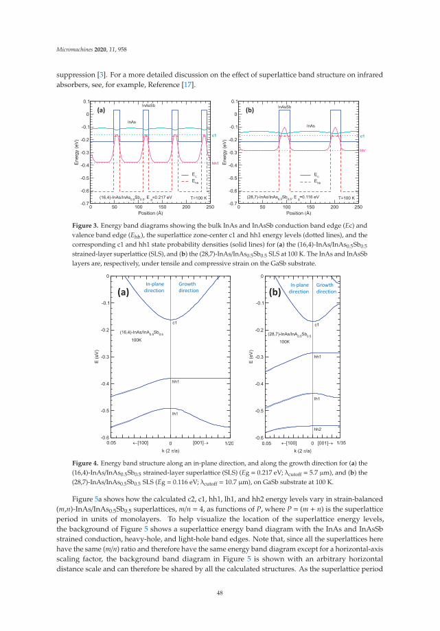
Micromachines 2020, 11, 958
suppression [3]. For a more detailed discussion on the effect of superlattice band structure on infraredabsorbers, see, for example, Reference [17].
(a) (b)
Figure 3. Energy band diagrams showing the bulk InAs and InAsSb conduction band edge (Ec) andvalence band edge (Ehh), the superlattice zone-center c1 and hh1 energy levels (dotted lines), and thecorresponding c1 and hh1 state probability densities (solid lines) for (a) the (16,4)-InAs/InAs0.5Sb0.5
strained-layer superlattice (SLS), and (b) the (28,7)-InAs/InAs0.5Sb0.5 SLS at 100 K. The InAs and InAsSblayers are, respectively, under tensile and compressive strain on the GaSb substrate.
(a) (b)Growth direction
In-plane direction
Growth direction
In-plane direction
Figure 4. Energy band structure along an in-plane direction, and along the growth direction for (a) the(16,4)-InAs/InAs0.5Sb0.5 strained-layer superlattice (SLS) (Eg = 0.217 eV; λcutoff = 5.7 μm), and (b) the(28,7)-InAs/InAs0.5Sb0.5 SLS (Eg = 0.116 eV; λcutoff = 10.7 μm), on GaSb substrate at 100 K.
Figure 5a shows how the calculated c2, c1, hh1, lh1, and hh2 energy levels vary in strain-balanced(m,n)-InAs/InAs0.5Sb0.5 superlattices, m/n = 4, as functions of P, where P = (m + n) is the superlatticeperiod in units of monolayers. To help visualize the location of the superlattice energy levels,the background of Figure 5 shows a superlattice energy band diagram with the InAs and InAsSbstrained conduction, heavy-hole, and light-hole band edges. Note that, since all the superlattices herehave the same (m/n) ratio and therefore have the same energy band diagram except for a horizontal-axisscaling factor, the background band diagram in Figure 5 is shown with an arbitrary horizontaldistance scale and can therefore be shared by all the calculated structures. As the superlattice period
48
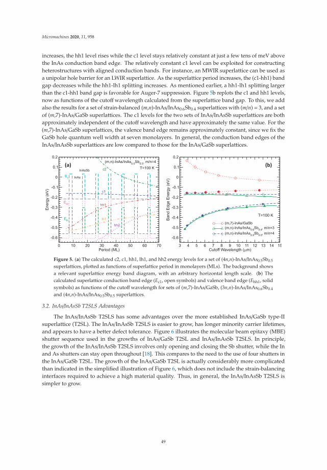
Micromachines 2020, 11, 958
increases, the hh1 level rises while the c1 level stays relatively constant at just a few tens of meV abovethe InAs conduction band edge. The relatively constant c1 level can be exploited for constructingheterostructures with aligned conduction bands. For instance, an MWIR superlattice can be used asa unipolar hole barrier for an LWIR superlattice. As the superlattice period increases, the (c1-hh1) bandgap decreases while the hh1-lh1 splitting increases. As mentioned earlier, a hh1-lh1 splitting largerthan the c1-hh1 band gap is favorable for Auger-7 suppression. Figure 5b replots the c1 and hh1 levels,now as functions of the cutoffwavelength calculated from the superlattice band gap. To this, we addalso the results for a set of strain-balanced (m,n)-InAs/InAs0.6Sb0.4 superlattices with (m/n) = 3, and a setof (m,7)-InAs/GaSb superlattices. The c1 levels for the two sets of InAs/InAsSb superlattices are bothapproximately independent of the cutoff wavelength and have approximately the same value. For the(m,7)-InAs/GaSb superlattices, the valence band edge remains approximately constant, since we fix theGaSb hole quantum well width at seven monolayers. In general, the conduction band edges of theInAs/InAsSb superlattices are low compared to those for the InAs/GaSb superlattices.
(a) (b)
Figure 5. (a) The calculated c2, c1, hh1, lh1, and hh2 energy levels for a set of (4n,n)-InAs/InAs0.5Sb0.5
superlattices, plotted as functions of superlattice period in monolayers (MLs). The background showsa relevant superlattice energy band diagram, with an arbitrary horizontal length scale. (b) Thecalculated superlattice conduction band edge (Ec1, open symbols) and valence band edge (Ehh1, solidsymbols) as functions of the cutoff wavelength for sets of (m,7)-InAs/GaSb, (3n,n)-InAs/InAs0.6Sb0.4
and (4n,n)-InAs/InAs0.5Sb0.5 superlattices.
3.2. InAs/InAsSb T2SLS Advantages
The InAs/InAsSb T2SLS has some advantages over the more established InAs/GaSb type-IIsuperlattice (T2SL). The InAs/InAsSb T2SLS is easier to grow, has longer minority carrier lifetimes,and appears to have a better defect tolerance. Figure 6 illustrates the molecular beam epitaxy (MBE)shutter sequence used in the growths of InAs/GaSb T2SL and InAs/InAsSb T2SLS. In principle,the growth of the InAs/InAsSb T2SLS involves only opening and closing the Sb shutter, while the Inand As shutters can stay open throughout [18]. This compares to the need to the use of four shutters inthe InAs/GaSb T2SL. The growth of the InAs/GaSb T2SL is actually considerably more complicatedthan indicated in the simplified illustration of Figure 6, which does not include the strain-balancinginterfaces required to achieve a high material quality. Thus, in general, the InAs/InAsSb T2SLS issimpler to grow.
49
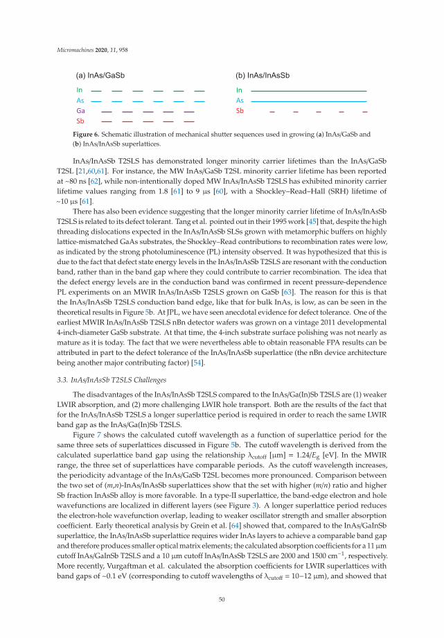
Micromachines 2020, 11, 958
InAsGaSb
InAsSb
Figure 6. Schematic illustration of mechanical shutter sequences used in growing (a) InAs/GaSb and(b) InAs/InAsSb superlattices.
InAs/InAsSb T2SLS has demonstrated longer minority carrier lifetimes than the InAs/GaSbT2SL [21,60,61]. For instance, the MW InAs/GaSb T2SL minority carrier lifetime has been reportedat ~80 ns [62], while non-intentionally doped MW InAs/InAsSb T2SLS has exhibited minority carrierlifetime values ranging from 1.8 [61] to 9 μs [60], with a Shockley–Read–Hall (SRH) lifetime of~10 μs [61].
There has also been evidence suggesting that the longer minority carrier lifetime of InAs/InAsSbT2SLS is related to its defect tolerant. Tang et al. pointed out in their 1995 work [45] that, despite the highthreading dislocations expected in the InAs/InAsSb SLSs grown with metamorphic buffers on highlylattice-mismatched GaAs substrates, the Shockley–Read contributions to recombination rates were low,as indicated by the strong photoluminescence (PL) intensity observed. It was hypothesized that this isdue to the fact that defect state energy levels in the InAs/InAsSb T2SLS are resonant with the conductionband, rather than in the band gap where they could contribute to carrier recombination. The idea thatthe defect energy levels are in the conduction band was confirmed in recent pressure-dependencePL experiments on an MWIR InAs/InAsSb T2SLS grown on GaSb [63]. The reason for this is thatthe InAs/InAsSb T2SLS conduction band edge, like that for bulk InAs, is low, as can be seen in thetheoretical results in Figure 5b. At JPL, we have seen anecdotal evidence for defect tolerance. One of theearliest MWIR InAs/InAsSb T2SLS nBn detector wafers was grown on a vintage 2011 developmental4-inch-diameter GaSb substrate. At that time, the 4-inch substrate surface polishing was not nearly asmature as it is today. The fact that we were nevertheless able to obtain reasonable FPA results can beattributed in part to the defect tolerance of the InAs/InAsSb superlattice (the nBn device architecturebeing another major contributing factor) [54].
3.3. InAs/InAsSb T2SLS Challenges
The disadvantages of the InAs/InAsSb T2SLS compared to the InAs/Ga(In)Sb T2SLS are (1) weakerLWIR absorption, and (2) more challenging LWIR hole transport. Both are the results of the fact thatfor the InAs/InAsSb T2SLS a longer superlattice period is required in order to reach the same LWIRband gap as the InAs/Ga(In)Sb T2SLS.
Figure 7 shows the calculated cutoff wavelength as a function of superlattice period for thesame three sets of superlattices discussed in Figure 5b. The cutoff wavelength is derived from thecalculated superlattice band gap using the relationship λcutoff [μm] = 1.24/Eg [eV]. In the MWIRrange, the three set of superlattices have comparable periods. As the cutoff wavelength increases,the periodicity advantage of the InAs/GaSb T2SL becomes more pronounced. Comparison betweenthe two set of (m,n)-InAs/InAsSb superlattices show that the set with higher (m/n) ratio and higherSb fraction InAsSb alloy is more favorable. In a type-II superlattice, the band-edge electron and holewavefunctions are localized in different layers (see Figure 3). A longer superlattice period reducesthe electron-hole wavefunction overlap, leading to weaker oscillator strength and smaller absorptioncoefficient. Early theoretical analysis by Grein et al. [64] showed that, compared to the InAs/GaInSbsuperlattice, the InAs/InAsSb superlattice requires wider InAs layers to achieve a comparable band gapand therefore produces smaller optical matrix elements; the calculated absorption coefficients for a 11μmcutoff InAs/GaInSb T2SLS and a 10 μm cutoff InAs/InAsSb T2SLS are 2000 and 1500 cm−1, respectively.More recently, Vurgaftman et al. calculated the absorption coefficients for LWIR superlattices withband gaps of ~0.1 eV (corresponding to cutoffwavelengths of λcutoff = 10−12 μm), and showed that
50
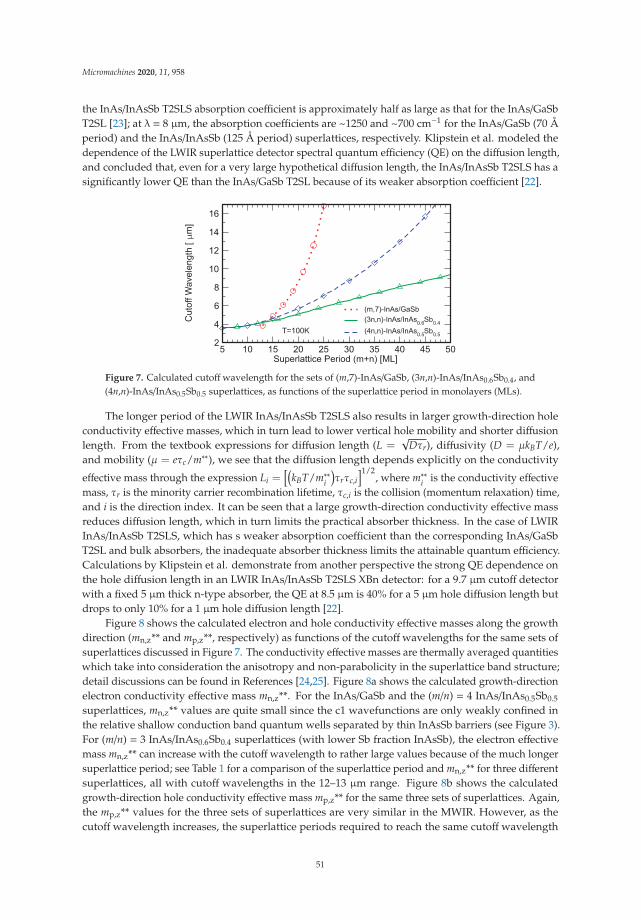
Micromachines 2020, 11, 958
the InAs/InAsSb T2SLS absorption coefficient is approximately half as large as that for the InAs/GaSbT2SL [23]; at λ = 8 μm, the absorption coefficients are ~1250 and ~700 cm−1 for the InAs/GaSb (70 Åperiod) and the InAs/InAsSb (125 Å period) superlattices, respectively. Klipstein et al. modeled thedependence of the LWIR superlattice detector spectral quantum efficiency (QE) on the diffusion length,and concluded that, even for a very large hypothetical diffusion length, the InAs/InAsSb T2SLS has asignificantly lower QE than the InAs/GaSb T2SL because of its weaker absorption coefficient [22].
Figure 7. Calculated cutoffwavelength for the sets of (m,7)-InAs/GaSb, (3n,n)-InAs/InAs0.6Sb0.4, and(4n,n)-InAs/InAs0.5Sb0.5 superlattices, as functions of the superlattice period in monolayers (MLs).
The longer period of the LWIR InAs/InAsSb T2SLS also results in larger growth-direction holeconductivity effective masses, which in turn lead to lower vertical hole mobility and shorter diffusionlength. From the textbook expressions for diffusion length (L =
√Dτr), diffusivity (D = μkBT/e),
and mobility (μ = eτc/m∗∗), we see that the diffusion length depends explicitly on the conductivity
effective mass through the expression Li =[(
kBT/m∗∗i)τrτc,i
]1/2, where m∗∗i is the conductivity effective
mass, τr is the minority carrier recombination lifetime, τc,i is the collision (momentum relaxation) time,and i is the direction index. It can be seen that a large growth-direction conductivity effective massreduces diffusion length, which in turn limits the practical absorber thickness. In the case of LWIRInAs/InAsSb T2SLS, which has s weaker absorption coefficient than the corresponding InAs/GaSbT2SL and bulk absorbers, the inadequate absorber thickness limits the attainable quantum efficiency.Calculations by Klipstein et al. demonstrate from another perspective the strong QE dependence onthe hole diffusion length in an LWIR InAs/InAsSb T2SLS XBn detector: for a 9.7 μm cutoff detectorwith a fixed 5 μm thick n-type absorber, the QE at 8.5 μm is 40% for a 5 μm hole diffusion length butdrops to only 10% for a 1 μm hole diffusion length [22].
Figure 8 shows the calculated electron and hole conductivity effective masses along the growthdirection (mn,z** and mp,z**, respectively) as functions of the cutoffwavelengths for the same sets ofsuperlattices discussed in Figure 7. The conductivity effective masses are thermally averaged quantitieswhich take into consideration the anisotropy and non-parabolicity in the superlattice band structure;detail discussions can be found in References [24,25]. Figure 8a shows the calculated growth-directionelectron conductivity effective mass mn,z**. For the InAs/GaSb and the (m/n) = 4 InAs/InAs0.5Sb0.5
superlattices, mn,z** values are quite small since the c1 wavefunctions are only weakly confined inthe relative shallow conduction band quantum wells separated by thin InAsSb barriers (see Figure 3).For (m/n) = 3 InAs/InAs0.6Sb0.4 superlattices (with lower Sb fraction InAsSb), the electron effectivemass mn,z** can increase with the cutoff wavelength to rather large values because of the much longersuperlattice period; see Table 1 for a comparison of the superlattice period and mn,z** for three differentsuperlattices, all with cutoff wavelengths in the 12–13 μm range. Figure 8b shows the calculatedgrowth-direction hole conductivity effective mass mp,z** for the same three sets of superlattices. Again,the mp,z** values for the three sets of superlattices are very similar in the MWIR. However, as thecutoff wavelength increases, the superlattice periods required to reach the same cutoff wavelength
51
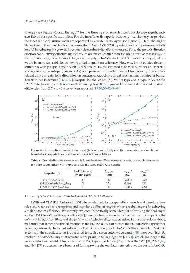
Micromachines 2020, 11, 958
diverge (see Figure 7), and the mp,z** for the three sets of superlattices also diverge significantly(see Table 1 for specific examples). For the InAs/InAsSb superlattices, mp,z** can be very large whenthe InAsSb hole quantum wells are separated by a wider InAs layer (see Figure 3). Here, the higherSb fraction in the InAsSb alloy decreases the InAs/InAsSb T2SLS period, and is therefore especiallyhelpful in reducing the growth-direction hole conductivity effective masses. Since the growth-directionelectron conductivity effective masses mn,z** are much smaller than the hole effective masses mp,z**,the diffusion length can be much longer in the p-type InAs/InAsSb T2SLS than in the n-type, whichwould be more favorable for achieving a higher quantum efficiency. However, for reticulated detectorstructures with p-type InAs/InAsSb T2SLS absorbers, the exposed side-wall surfaces are invertedto degenerate the n-type (like in InAs) and passivation is often needed for reducing the surfacerelated dark currents; for a discussion on surface leakage dark current mechanisms in unipolar barrierdetectors, see Reference [34,65–67]. Despite the challenges, (V)LWIR n-type and p-type InAs/InAsSbT2SLS detectors with cutoff wavelengths ranging from 8 to 15 μm and front-side illuminated quantumefficiencies from 2.5% to 40% have been reported [19,20,50–52,68,69].
(a) (b)
Figure 8. Growth-direction (a) electron and (b) hole conductivity effective masses for two families ofInAs/InAsSb superlattices, and a set of InAs/GaSb superlattices.
Table 1. Growth direction electron and hole conductivity effective masses in units of bare electron massfor three superlattices with approximately the same cutoffwavelength.
SuperlatticePeriod (m + n)[monolayer]
λcutoff
[μm]mn,z**[m0]
mp,z**[m0]
(16,7)-InAs/GaSb 23 12.5 0.0233 1.29(54,18)-InAs/InAs0.6Sb0.4 72 12.0 0.166 222(32,8)-InAs/InAs0.5Sb0.5 40 13.0 0.0313 7.89
3.4. Concepts for Addressing LWIR InAs/InAsSb T2SLS Challenges
LWIR and VLWIR InAs/InAsSb T2SLS have relatively long superlattice periods and therefore haverelatively weak optical absorptions and short hole diffusion lengths, which are challenging for achievinga high quantum efficiency. We recently explored theoretically some ideas for addressing the challengesfor the LWIR InAs/InAsSb superlattices [70]; here, we briefly summarize the results. In comparing the(m/n) = 3 InAs/InAs0.6Sb0.4 and the (m/n) = 4 InAs/InAs0.5Sb0.5 superlattices in the discussions above,we found that increasing the Sb fraction in the InAsSb alloy can reduce the InAs/InAsSb superlatticeperiod significantly. In fact, at sufficiently high Sb fraction (~75%), InAs/InAsSb can match InAs/GaSbin terms of the superlattice period required to reach a given cutoff wavelength [70]. However, high Sbfraction InAs/InAsSb superlattices are more prone to Sb segregation [71–74], which can negate theperiod-reduction benefit of high-fraction Sb. Polytype superlattices [75] such as the “W” [31], “M” [76],and “N” [77] structures have been used for improving the oscillator strength over the basic InAs/GaSb
52
Micromachines 2020, 11, 958
T2SL. The analogous polytype W, M, and N superlattices formed by inserting thin AlAsSb barrier layersin InAs/InAsSb T2SLS have been considered as a means for increasing electron-hole wavefunctionoverlap for stronger optical absorption. This strategy turns out to be unfavorable because the presenceof the AlAsSb barriers leads to increased band gap, and therefore increases the superlattice periodrequired to reach a given cutoff wavelength [70]. Metamorphic growth on virtual substrates withlarger lattice constants than GaSb can decrease the superlattice period needed to reach a specifiedcutoffwavelength, but this benefit should be weighed against the need for metamorphic buffer growthand the resulting higher defect density [70]. Finally, as mentioned previously, p-type InAs/InAsSbT2SLS has a longer diffusion length than n-type, but reticulated detector pixels with exposed p-typeabsorber side-wall surface would require passivation to suppress the surface leakage dark current.
4. Recent Development and Outlook
InAs/InAsSb T2SLS infrared detectors have been under very active development in recent years,with reported results by research groups worldwide in MWIR [18,56,57,78–82], LWIR [19,20,50,51,83,84],and VLWIR [52,85] detectors, as well as in MWIR/LWIR [53] and LWIR/VLWIR [68] bias-switchabledual-band detectors. Microlens [85] and resonant cavity structures [86] have been used to enhancethe photo-response of InAs/InAsSb T2SLS infrared detectors. Studies of transport properties [87–90]and defect levels [63] have led to an improved understanding of InAs/InAsSb superlattices. Whilemost of the more recent InAs/InAsSb T2SLS structures have been grown on (100) GaSb substrates byMBE, growths by a variety of modes have also been demonstrated. MWIR and LWIR detectors havebeen grown by metal organic chemical vapor deposition (MOCVD) [91–94]. Growths on GaAs [84],Si [80,95], Ge-Si [96], and AlSb (via metamorphic buffer on GaSb) [97] substrates have been reported.The growth of MWIR and LWIR detectors on (211)A and B, and (311)A and B GaSb substrates havealso been demonstrated [69,98].
The MWIR InAs/InAsSb T2SLS FPA rivals InSb in manufacturability and affordability, but offersa 40 to 50 K higher operating temperature advantage, which can lead to a lower cryocooler size, weight,and power (SWaP). As such, it is poised to replace the InSb FPA, a major incumbent technology, in manyimaging applications. The MWIR InAs/InAsSb T2SLS detectors and FPAs have also demonstrated verylow dark current densities at lower temperatures [99], and are therefore suitable for more demandingapplications such as the CubeSat-based hyperspectral imaging of 300 K scenes while operating in anintermediate temperature range (100–120 K) [100]. Although LWIR InAs/InAsSb T2SLS FPAs haveonly achieved a moderate quantum efficiency, their demonstrated large-format capability and highuniformity and operability makes them already suitable for applications such as LWIR imaging forEarth remote sensing applications, where photon flux is abundant. Dual-band FPAs are also expectedto find applications because of the manufacturability and cost effectiveness of InAs/InAsSb T2SLS FPAs.The further development of InAs/InAsSb T2SLS infrared detectors will continue to benefit from theinfrastructure established largely during the the VISTA Program [101,102], including the availability oflarge-diameter format GaSb substrates [103–106] and multi-wafer growth capability at commercialfoundries [107,108].
Funding: The research was carried out at the Jet Propulsion Laboratory, California Institute of Technology, under acontract with the National Aeronautics and Space Administration (80NM0018D0004).
Acknowledgments: The authors would like to thank S. Bandara, A.J. Ciani, R.E. DeWames, D. Forrai, C.H. Grein,L. Höglund, M.A. Kinch, P.C. Klipstein, A.W.K. Liu, D. Lubyshev, S. Maimon, T.S. Pagano, P. Pinsukanjana,D.R. Rhiger, J.N. Schulman, W.E. Tennant, M.Z. Tidrow, Y. Wei, G.W. Wicks, R.Q. Yang, and Y.-H. Zhang forhelpful discussions.
Conflicts of Interest: The authors declare no conflict of interest.
53
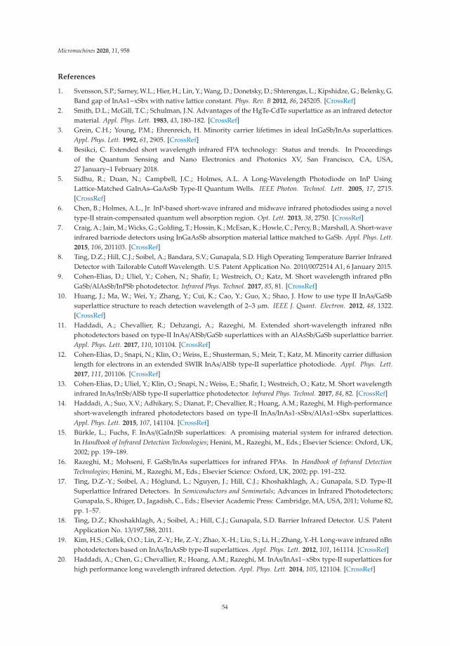
Micromachines 2020, 11, 958
References
1. Svensson, S.P.; Sarney, W.L.; Hier, H.; Lin, Y.; Wang, D.; Donetsky, D.; Shterengas, L.; Kipshidze, G.; Belenky, G.Band gap of InAs1−xSbx with native lattice constant. Phys. Rev. B 2012, 86, 245205. [CrossRef]
2. Smith, D.L.; McGill, T.C.; Schulman, J.N. Advantages of the HgTe-CdTe superlattice as an infrared detectormaterial. Appl. Phys. Lett. 1983, 43, 180–182. [CrossRef]
3. Grein, C.H.; Young, P.M.; Ehrenreich, H. Minority carrier lifetimes in ideal InGaSb/InAs superlattices.Appl. Phys. Lett. 1992, 61, 2905. [CrossRef]
4. Besikci, C. Extended short wavelength infrared FPA technology: Status and trends. In Proceedingsof the Quantum Sensing and Nano Electronics and Photonics XV, San Francisco, CA, USA,27 January–1 February 2018.
5. Sidhu, R.; Duan, N.; Campbell, J.C.; Holmes, A.L. A Long-Wavelength Photodiode on InP UsingLattice-Matched GaInAs–GaAsSb Type-II Quantum Wells. IEEE Photon. Technol. Lett. 2005, 17, 2715.[CrossRef]
6. Chen, B.; Holmes, A.L., Jr. InP-based short-wave infrared and midwave infrared photodiodes using a noveltype-II strain-compensated quantum well absorption region. Opt. Lett. 2013, 38, 2750. [CrossRef]
7. Craig, A.; Jain, M.; Wicks, G.; Golding, T.; Hossin, K.; McEsan, K.; Howle, C.; Percy, B.; Marshall, A. Short-waveinfrared barriode detectors using InGaAsSb absorption material lattice matched to GaSb. Appl. Phys. Lett.2015, 106, 201103. [CrossRef]
8. Ting, D.Z.; Hill, C.J.; Soibel, A.; Bandara, S.V.; Gunapala, S.D. High Operating Temperature Barrier InfraredDetector with Tailorable CutoffWavelength. U.S. Patent Application No. 2010/0072514 A1, 6 January 2015.
9. Cohen-Elias, D.; Uliel, Y.; Cohen, N.; Shafir, I.; Westreich, O.; Katz, M. Short wavelength infrared pBnGaSb/AlAsSb/InPSb photodetector. Infrared Phys. Technol. 2017, 85, 81. [CrossRef]
10. Huang, J.; Ma, W.; Wei, Y.; Zhang, Y.; Cui, K.; Cao, Y.; Guo, X.; Shao, J. How to use type II InAs/GaSbsuperlattice structure to reach detection wavelength of 2–3 μm. IEEE J. Quant. Electron. 2012, 48, 1322.[CrossRef]
11. Haddadi, A.; Chevallier, R.; Dehzangi, A.; Razeghi, M. Extended short-wavelength infrared nBnphotodetectors based on type-II InAs/AlSb/GaSb superlattices with an AlAsSb/GaSb superlattice barrier.Appl. Phys. Lett. 2017, 110, 101104. [CrossRef]
12. Cohen-Elias, D.; Snapi, N.; Klin, O.; Weiss, E.; Shusterman, S.; Meir, T.; Katz, M. Minority carrier diffusionlength for electrons in an extended SWIR InAs/AlSb type-II superlattice photodiode. Appl. Phys. Lett.2017, 111, 201106. [CrossRef]
13. Cohen-Elias, D.; Uliel, Y.; Klin, O.; Snapi, N.; Weiss, E.; Shafir, I.; Westreich, O.; Katz, M. Short wavelengthinfrared InAs/InSb/AlSb type-II superlattice photodetector. Infrared Phys. Technol. 2017, 84, 82. [CrossRef]
14. Haddadi, A.; Suo, X.V.; Adhikary, S.; Dianat, P.; Chevallier, R.; Hoang, A.M.; Razeghi, M. High-performanceshort-wavelength infrared photodetectors based on type-II InAs/InAs1-xSbx/AlAs1-xSbx superlattices.Appl. Phys. Lett. 2015, 107, 141104. [CrossRef]
15. Bürkle, L.; Fuchs, F. InAs/(GaIn)Sb superlattices: A promising material system for infrared detection.In Handbook of Infrared Detection Technologies; Henini, M., Razeghi, M., Eds.; Elsevier Science: Oxford, UK,2002; pp. 159–189.
16. Razeghi, M.; Mohseni, F. GaSb/InAs superlattices for infrared FPAs. In Handbook of Infrared DetectionTechnologies; Henini, M., Razeghi, M., Eds.; Elsevier Science: Oxford, UK, 2002; pp. 191–232.
17. Ting, D.Z.-Y.; Soibel, A.; Höglund, L.; Nguyen, J.; Hill, C.J.; Khoshakhlagh, A.; Gunapala, S.D. Type-IISuperlattice Infrared Detectors. In Semiconductors and Semimetals; Advances in Infrared Photodetectors;Gunapala, S., Rhiger, D., Jagadish, C., Eds.; Elsevier Academic Press: Cambridge, MA, USA, 2011; Volume 82,pp. 1–57.
18. Ting, D.Z.; Khoshakhlagh, A.; Soibel, A.; Hill, C.J.; Gunapala, S.D. Barrier Infrared Detector. U.S. PatentApplication No. 13/197,588, 2011.
19. Kim, H.S.; Cellek, O.O.; Lin, Z.-Y.; He, Z.-Y.; Zhao, X.-H.; Liu, S.; Li, H.; Zhang, Y.-H. Long-wave infrared nBnphotodetectors based on InAs/InAsSb type-II superlattices. Appl. Phys. Lett. 2012, 101, 161114. [CrossRef]
20. Haddadi, A.; Chen, G.; Chevallier, R.; Hoang, A.M.; Razeghi, M. InAs/InAs1−xSbx type-II superlattices forhigh performance long wavelength infrared detection. Appl. Phys. Lett. 2014, 105, 121104. [CrossRef]
54

Micromachines 2020, 11, 958
21. Steenbergen, E.H.; Connelly, B.C.; Metcalfe, G.D.; Shen, H.; Wraback, M.; Lubyshev, D.; Qiu, Y.; Fastenau, J.M.;Liu, A.W.K.; Elhamri, S.; et al. Significantly improved minority carrier lifetime observed in a long-wavelengthinfrared III-V type-II superlattice comprised of InAs/InAsSb. Appl. Phys. Lett. 2011, 99, 251110. [CrossRef]
22. Klipstein, P.C.; Livneh, Y.; Glozman, A.; Grossman, S.; Klin, O.; Snapi, N.; Weiss, E. Modeling InAs/GaSb andInAs/InAsSb Superlattice Infrared Detectors. J. Electron. Mater. 2014, 43, 2984. [CrossRef]
23. Vurgaftman, I.; Belenky, G.; Lin, Y.; Donetsky, D.; Shterengas, L.; Kipshidze, G.; Sarney, W.L.; Svensson, S.P.Interband absorption strength in long-wave infrared type-II superlattices with small and large superlatticeperiods compared to bulk materials. Appl. Phys. Lett. 2016, 108, 222101. [CrossRef]
24. Ting, D.Z.; Soibel, A.; Gunapala, S.D. Hole effective masses and subband splitting in type-II superlatticeinfrared detectors. Appl. Phys. Lett. 2016, 108, 183504. [CrossRef]
25. Ting, D.Z.; Soibel, A.; Gunapala, S.D. Type-II superlattice hole effective masses. Infrared Phys. Technol.2017, 84, 102–106. [CrossRef]
26. Maimon, S.; Wicks, G.W. nBn detector, an infrared detector with reduced dark current and higher operatingtemperature. Appl. Phys. Lett. 2006, 89, 151109. [CrossRef]
27. Klipstein, P. Depletion-Less Photodiode with Suppressed Dark Current and Method for Producing the Same.Int. Patent Publication No: WO 2005/004243 A1, 2005.
28. Klipstein, P.C. XBn barrier photodetectors for high sensitivity and high operating temperature infrared sensors.In Proceedings of the Infrared Technology and Applications XXXIV, Orlando, FL, USA, 16–20 March 2008.
29. Ting, D.Z.-Y.; Hill, C.J.; Soibel, A.; Keo, S.A.; Mumolo, J.M.; Nguyen, J.; Gunapala, S.D. A high-performancelong wavelength superlattice complementary barrier infrared detector. Appl. Phys. Lett. 2009, 95, 023508.[CrossRef]
30. Ting, D.Z.-Y.; Soibel, A.; Khoshakhlagh, A.; Nguyen, J.; Höglund, L.; Keo, S.A.; Mumolo, J.M.; Gunapala, S.D.Exclusion, extraction, and junction placement effects in the complementary barrier infrared detector.Appl. Phys. Lett. 2013, 102, 121109. [CrossRef]
31. Canedy, C.L.; Aifer, E.H.; Vurgaftman, I.; Tischler, J.G.; Meyer, J.R.; Warner, J.H.; Jackson, E.M. AntimonideType-II “W” Photodiodes with Long-Wave Infrared R0A Comparable to HgCdTe. J. Electron. Mater. 2007, 36,852–856. [CrossRef]
32. Nguyen, B.-M.; Hoffman, D.; Delaunay, P.-Y.; Razeghi, M. Dark current suppression in type IIInAs/GaSbInAs/GaSb superlattice long wavelength infrared photodiodes with M-structure barrier.Appl. Phys. Lett. 2007, 91, 163511. [CrossRef]
33. Nguyen, B.M.; Chen, G.; Hoang, A.M.; Abdollahi Pour, S.; Bogdanov, S.; Razeghi, M. Effect of contact dopingin superlattice-based minority carrier unipolar detectors. Appl. Phys. Lett. 2011, 99, 033501. [CrossRef]
34. Wicks, G.W.; Savich, G.R.; Pedrazzani, J.R.; Maimon, S. Infrared detector epitaxial designs for suppressionof surface leakage current. In Proceedings of the Quantum Sensing and Nanophotonic Devices VII,San Francisco, CA, USA, 23–28 January 2010.
35. Savich, G.R.; Pedrazzani, J.R.; Sidor, D.E.; Maimon, S.; Wicks, G.W. Dark current filtering in unipolar barrierinfrared detectors. Appl. Phys. Lett. 2011, 99, 121112. [CrossRef]
36. Rodriguez, J.B.; Plis, E.; Bishop, G.; Sharma, Y.D.; Kim, H.; Dawson, L.R.; Krishna, S. nBn structure based onInAs/GaSb type-II strained layer superlattices. Appl. Phys. Lett. 2007, 91, 043514. [CrossRef]
37. Smith, D.L.; Mailhiot, C. Proposal for strained type II superlattice infrared detectors. Appl. Phys. Lett.1987, 34, 663–665. [CrossRef]
38. Osbourn, G.C. Electro-Optical SLS Devices for Operating at New Wavelength Ranges. U.S. Patent No.4,607,272, 19 August 1986.
39. Osbourn, G.C. InAsSb Strained layer superlattices for long wavelength detector applications. J. Vac. Sci.Technol. B 1984, 2, 176. [CrossRef]
40. Osbourn, G.C.; Dawson, L.R.; Biefeld, R.M.; Zipperlan, T.E.; Fritz, I.J.; Doyle, B.L. III-V strained layersuperlattices for long-wavelength detector applications: Recent progress. J. Vac. Sci. Technol. A 1987, 5,3150–3152. [CrossRef]
41. Kurtz, S.R.; Dawson, L.R.; Zipperian, T.E.; Lee, S.R. Demonstration of an InAsSb strained layer superlatticephotodiode. Appl. Phys. Lett. 1988, 52, 1581. [CrossRef]
42. Kurtz, S.R.; Dawson, L.R.; Biefeld, R.M.; Fritz, I.J.; Zipperian, T.E. Long wavelength InAsSb strained layersuperlattice photovoltaic infrared detector. IEEE Elect. Device Lett. 1989, 10, 150–152. [CrossRef]
55
Micromachines 2020, 11, 958
43. Kurtz, S.R.; Biefeld, R.M.; Zipperlan, T.E. MOCVD-grown InAsSb strained-layer superlattice infrareddetectors with photoresponses ≥ 10 μm. Semicond. Sci. Technol. 1990, 5, S24–S26. [CrossRef]
44. Zhang, Y.-H. Continuous wave operation of InAs/InAsxSb12x midinfrared lasers. Appl. Phys. Lett. 1995, 66,118–120. [CrossRef]
45. Tang, P.J.P.; Pullin, M.J.; Chung, S.J.; Phillips, C.C.; Stradling, R.A.; Norman, A.G.; Li, Y.B.; Hart, L.4–11 pm infrared emission and 300 K light emitting diodes from arsenic-rich InAs/InAs1-xSbx strained layersuperlattices. Semicond. Sci. Technol. 1995, 10, 1177–1180. [CrossRef]
46. Ciesla, C.M.; Murdin, B.N.; Pidgeon, C.R.; Stradling, R.A.; Phillips, C.C.; Livingstone, M.; Galbraith, I.;Jaroszynski, D.A.; Langerak, C.J.G.M.; Tang, P.J.P.; et al. Suppression of Auger recombination in arsenic-richInAs1-xSbx strained layer superlattices. J. Appl. Phys. 1996, 80, 2994. [CrossRef]
47. Pullin, M.J.; Hardaway, H.R.; Heber, J.D.; Phillips, C.C.; Yuen, W.T.; Stradling, R.A. Room-temperatureInAsSb strained-layer superlattice light-emitting diodes at λ = 4.2 μm with AlSb barriers for improved carrierconfinement. Appl. Phys. Lett. 1999, 74, 2384–2386.
48. Chow, D.H.; Miles, R.H.; Söderström, J.R.; McGill, T.C. Growth and characterization of InAs/Ga1-xInxSbstrained-layer superlattices. Appl. Phys. Lett. 1990, 56, 1418–1420. [CrossRef]
49. Lackner, D.; Pitts, O.J.; Steger, M.; Yang, A.; Thewalt, M.L.W.; Watkins, S.P. Strain balanced InAs/InAsSbsuperlattice structures with optical emission to 10 μm. Appl. Phys. Lett. 2009, 95, 081906. [CrossRef]
50. Haddadi, A.; Dehzangi, A.; Adhikary, S.; Chevallier, R.; Razeghi, M. Background–limited long wavelengthinfrared InAs/InAs1− xSbx type-II superlattice-based photodetectors operating at 110 K. APL Mater.2017, 5, 035502. [CrossRef]
51. Chevallier, R.; Haddadi, A.; Razeghi, M. Dark current reduction in microjunction-based double electronbarrier type-II InAs/InAsSb superlattice long-wavelength infrared photodetectors. Sci. Rep. 2017, 7, 12617.[CrossRef] [PubMed]
52. Hoang, A.M.; Chen, G.; Chevallier, R.; Haddadi, A.; Razeghi, M. High performance photodiodes basedon InAs/InAsSb type-II superlattices for very long wavelength infrared detection Appl. Phys. Lett.2014, 104, 251105.
53. Haddadi, A.; Chevallier, R.; Chen, G.; Hoang, A.M.; Razeghi, M. Bias-selectable dual-bandmid-/long-wavelength infrared photodetectors based on InAs/InAs1−xSbx type-II superlattices.Appl. Phys. Lett. 2015, 106, 011104. [CrossRef]
54. Ting, D.Z.; Soibel, A.; Khoshakhlagh, A.; Keo, S.A.; Rafol, S.B.; Höglund, L.; Luong, E.M.; Fisher, A.M.;Hill, C.J.; Gunapala, S.D. Development of InAs/InAsSb Type II Strained-Layer Superlattice Unipolar BarrierInfrared Detectors. J. Electron. Mater. 2019, 48, 6145–6151. [CrossRef]
55. Ting, D.Z.; Soibel, A.; Khoshakhlagh, A.; Keo, S.A.; Rafol, S.B.; Fisher, A.M.; Hill, C.J.; Luong, E.M.;Pepper, B.J.; Gunapala, S.D. The emergence of InAs/InAsSb type-II strained layer superlattice barrier infrareddetectors. In Proceedings of the SPIE 11002, Infrared Technology and Applications XLV, Baltimore, MD,USA, 14–18 April 2019; p. 110020F.
56. Ting, D.Z.; Soibel, A.; Khoshakhlagh, A.; Rafol, S.B.; Keo, S.; Höglund, L.; Fisher, A.M.; Luong, E.M.;Gunapala, S.D. Mid-wavelength high operating temperature barrier infrared detector and focal plane array.Appl. Phys. Lett. 2018, 113, 021101. [CrossRef]
57. Ting, D.Z.; Rafol, S.B.; Keo, S.; Nguyen, J.; Khoshakhlagh, A.; Soibel, A.; Hoglund, L.; Fisher, A.M.;Luong, E.M.; Mumolo, J.; et al. InAs/InAsSb Type-II Superlattice Mid-Wavelength Infrared Focal Plane Arraywith Significantly Higher Operating Temperature Than InSb. IEEE Photon. J. 2018, 10, 6804106. [CrossRef]
58. Tennant, W.E. “Rule 07” Revisited: Still a Good Heuristic Predictor of p/n HgCdTe Photodiode Performance?J. Electron. Mater. 2010, 39, 1030. [CrossRef]
59. Klipstein, P.C.; Aronov, D.; Ben Ezra, M.; Barkai, I.; Berkowicz, E.; Brumer, M.; Fraenkel, R.; Glozman, A.;Grossman, S.; Jacobsohn, E.; et al. Recent progress in InSb based quantum detectors in Israel.Infrared Phys. Technol. 2013, 59, 172–181. [CrossRef]
60. Olson, B.V.; Shaner, E.A.; Kim, J.K.; Klem, J.F.; Hawkins, S.D.; Murray, L.M.; Prineas, J.P.; Flatté, M.E.;Boggess, T.F. Time-resolved optical measurements of minority carrier recombination in a mid-wave infraredInAsSb alloy and InAs/InAsSb superlattice. Appl. Phys. Lett. 2012, 101, 092109. [CrossRef]
61. Höglund, L.; Ting, D.Z.; Khoshakhlagh, A.; Soibel, A.; Hill, C.J.; Fisher, A.; Keo, S.; Gunapala, S.D. Influence ofradiative and non-radiative recombination on the minority carrier lifetime in midwave infrared InAs/InAsSbsuperlattices. Appl. Phys. Lett. 2013, 103, 221908. [CrossRef]
56
Micromachines 2020, 11, 958
62. Donetsky, D.; Svensson, S.P.; Vorobjev, L.E.; Belenky, G. Carrier lifetime measurements in short-periodInAs/GaSb strained-layer superlattice structures. Appl. Phys. Lett. 2009, 95, 212104. [CrossRef]
63. Prins, A.D.; Lewis, M.K.; Bushell, Z.L.; Sweeney, S.J.; Liu, S.; Zhang, Y.-H. Evidence for a defect levelabove the conduction band edge of InAs/InAsSb type-II superlattices for applications in efficient infraredphotodetectors. Appl. Phys. Lett. 2015, 106, 171111. [CrossRef]
64. Grein, C.H.; Flatté, M.E.; Ehrenreich, H. Comparison of Ideal InAs/InAs1-xSbx and InAs/InxGa1-xSbSuperlattice IR Detectors. In Proceedings of the Third International Symposium on Long-WavelengthInfrared Detectors and Arrays: Physics and Applications, Chicago, IL, USA, 8–13 October 1995; Li, S.S.,Liu, H.C., Beck, W.A., Tidrow, M.Z., Singh, A., Eds.; Electrochemical Society: Pennington, NJ, USA, 1995;Volume 95–28, pp. 211–218.
65. Sidor, D.E.; Savich, G.R.; Wicks, G.W. Surface Leakage Mechanisms in III–V Infrared Barrier Detectors.J. Electron. Mater. 2016, 45, 4663–4667. [CrossRef]
66. Du, X.; Marozas, B.T.; Savich, G.R.; Wicks, G.W. Defect-related surface currents in InAs-based nBn infrareddetectors. J. Appl. Phys. 2018, 123, 214504. [CrossRef]
67. Marozas, B.T.; Hughes, W.D.; Du, X.; Sidor, D.E.; Savich, G.R.; Wicks, G.W. Surface dark current mechanismsin III-V infrared photodetectors. Opt. Mater. Express 2018, 8, 1419–1424. [CrossRef]
68. Haddadi, A.; Dehzangi, A.; Chevallier, R.; Adhikary, S.; Razeghi, M. Bias-selectable nBn dual-band long-/verylong-wavelength infrared photodetectors based on InAs/InAs1-xSbx/AlAs1-xSbx type-II superlattices.Sci. Rep. 2017, 7, 3379. [CrossRef] [PubMed]
69. Lubyshev, D.; Fastenau, J.M.; Kattner, M.; Frey, P.; Nelson, S.A.; Liu, A.W.K.; Martinez, B.; Furlong, M.J. T2SLMid- and long- wave infrared photodetector structures grown on (211)A, (211)B, and (311)A GaSb substrates.In Proceedings of the SPIE 11002, Infrared Technology and Applications XLV, Baltimore, MD, USA, 14–18April 2019; pp. 11002–11023.
70. Ting, D.Z.; Khoshakhlagh, A.; Soibel, A.; Gunapala, S.D. Long Wavelength InAs/InAsSb Infrared SuperlatticeChallenges: A Theoretical Investigation. J. Electron. Mater. 2020. [CrossRef]
71. Ciani, A.J.; Grein, C.H.; Irick, B.; Miao, M.S.; Kioussis, N. Molecular dynamics growth modeling ofInAs1−xSbx-based type-II superlattice. Opt. Eng. 2017, 56, 091609. [CrossRef]
72. Haugan, H.J.; Brown, G.J.; Peoples, J.A. On the study of antimony incorporation in InAs/InAsSb superlatticesfor infrared sensing. J. Vac. Sci. Technol. B 2017, 35, 02B107. [CrossRef]
73. Sarney, W.L.; Svensson, S.P.; Yakes, M.K.; Xu, Y.; Donetsky, D.; Belenky, G. Ultra-short period Ga-freesuperlattice growth on GaSb. J. Appl. Phys. 2018, 124, 035304. [CrossRef]
74. Kanedy, K.; Lopez, F.; Wood, M.R.; Gmachl, C.F.; Weimer, M.; Klem, J.F.; Hawkins, S.D.; Shaner, E.A.;Kim, J.K. Visualizing period fluctuations in strained-layer superlattices with scanning tunneling microscopy.Appl. Phys. Lett. 2018, 112, 042105. [CrossRef]
75. Esaki, L.; Chang, L.L.; Mendez, E.E. Polytype Superlattices and Multi-Heterojunctions. Jpn. J. Appl. Phys.1981, 20, L529–L532. [CrossRef]
76. Delaunay, P.Y.; Nguyen, B.M.; Hoffman, D.; Huang, E.K.W.; Razeghi, M. Background Limited Performanceof Long Wavelength Infrared Focal Plane Arrays Fabricated From M-Structure InAs–GaSb Superlattices.IEEE J. Quantum Electron. 2009, 45, 157–162. [CrossRef]
77. Salihoglu, O.; Muti, A.; Kutluer, K.; Tansel, T.; Turan, R.; Ergun, Y.; Aydinli, A. “N” structure for type-IIsuperlattice photodetectors. Appl. Phys. Lett. 2012, 101, 073505. [CrossRef]
78. Hao, R.; Ren, Y.; Liu, S.; Guo, J.; Wang, G.; Xu, Y.; Niu, Z. Fabrication and characterization of high latticematched InAs/InAsSb superlattice infrared photodetector. J. Cryst. Growth 2017, 470, 33. [CrossRef]
79. Craig, A.P.; Al-Saymari, F.; Jain, M.; Bainbridge, A.; Savich, G.R.; Golding, T.; Krier, A.; Wicks, G.W.;Marshall, A.R. Resonant cavity enhanced photodiodes on GaSb for the mid-wave infrared. Appl. Phys. Lett.2019, 114, 151107. [CrossRef]
80. Durlin, Q.; Perez, J.P.; Cerutti, L.; Rodriguez, J.B.; Cerba, T.; Baron, T.; Tournie, E.; Christol, P. Midwaveinfrared barrier detector based on Ga-free InAs/InAsSb type-II superlattice grown by molecular beam epitaxyon Si substrate. Infrared Phys. Technol. 2019, 96, 39–43. [CrossRef]
81. Ariyawansa, G.; Duran, J.; Reyner, C.; Scheihing, J. InAs/InAsSb Strained-Layer Superlattice Mid-WavelengthInfrared Detector for High-Temperature Operation. Micromachines 2019, 10, 806. [CrossRef]
57
Micromachines 2020, 11, 958
82. Deng, G.; Song, X.; Pan, M.; Xiao, T.; Luo, Z.; Chen, N.; Yang, W.; Zhang, Y. Upside-down InAs/InAs1-xSbxtype-II superlattice-based nBn mid-infrared photodetectors with an AlGaAsSb quaternary alloy barrier.Opt. Express 2020, 28, 13616–13624. [CrossRef]
83. Manyk, T.; Michalczewski, K.; Murawski, K.; Martyniuk, P.; Rutkowski, J. InAs/InAsSb Strain-BalancedSuperlattices for Longwave Infrared Detectors. Sensors 2019, 19, 1907. [CrossRef]
84. Michalczewski, K.; Kubiszyn, Ł.; Martyniuk, P.; Wu, C.H.; Jurenczyk, J.; Grodecki, K.; Benyahia, D.;Rogalski, A.; Piotrowski, J. Demonstration of HOT LWIR T2SLs InAs/InAsSb photodetectors grown on GaAssubstrate. Infrared Phys. Technol. 2018, 95, 222. [CrossRef]
85. Michalczewski, K.; Martyniuk, P.; Kubiszyn, L.; Wu, C.H.; Wu, Y.R.; Jurenczyk, J.; Rogalski, A.; Piotrowski, J.Demonstration of the Very Long Wavelength Infrared Type-II Superlattice InAs/InAsSb GaAs ImmersedPhotodetector Operating at Thermoelectric Cooling. IEEE Electron Device Lett. 2019, 40, 1396–1398. [CrossRef]
86. Letka, V.; Bainbridge, A.; Craig, A.P.; Al-Saymari, F.; Marshall, A.R.J. Resonant cavity-enhanced photodetectorincorporating a type-II superlattice to extend MWIR sensitivity. Opt. Express 2019, 27, 23970–23980. [CrossRef][PubMed]
87. Yeche, A.; Boulard, F.; Cervera, C.; Perez, J.P.; Rodriguez, J.B.; Christol, P.; Gravrand, O. Development ofElectron Beam Induced Current for diffusion length determination of VLWIR HgCdTe and MWIR T2SLbased photodetectors. Infrared Phys. Technol. 2018, 95, 170–176. [CrossRef]
88. Rhiger, D.R.; Smith, E.P. Carrier Transport in the Valence Band of nBn III-V Superlattice Infrared Detectors.J. Electron. Mater. 2019, 48, 6053–6062. [CrossRef]
89. Casias, L.K.; Morath, C.P.; Steenbergen, E.H.; Umana-Membreno, G.A.; Webster, P.T.; Logan, J.V.; Kim, J.K.;Balakrishnan, G.; Faraone, L.; Krishna, S. Vertical carrier transport in strain-balanced InAs/InAsSb type-IIsuperlattice material. Appl. Phys. Lett. 2019, 116, 182109. [CrossRef]
90. Tsai, C.Y.; Zhang, Y.; Ju, Z.; Zhang, Y.H. Study of vertical hole transport in InAs/InAsSb type-II superlatticesby steady-state and time-resolved photoluminescence spectroscopy. Appl. Phys. Lett. 2020, 116, 201108.[CrossRef]
91. Huang, Y.; Ryou, J.-H.; Dupuis, R.D.; D’Costa, V.R.; Steenbergen, E.H.; Fan, J.; Zhang, Y.-H.; Petschke, A.;Mandl, M.; Chuang, S.-L. Epitaxial growth and characterization of InAs/GaSb and InAs/InAsSb type-IIsuperlattices on GaSb substrates by metalorganic chemical vapor deposition for long wavelength infraredphotodetectors. J. Cryst. Growth 2011, 314, 92–96. [CrossRef]
92. Wu, D.H.; Durlin, Q.; Dehzangi, A.; Zhang, Y.; Razeghi, M. High quantum efficiency mid-wavelength infraredtype-II InAs/InAs1−xSbx superlattice photodiodes grown by metal-organic chemical vapor deposition.Appl. Phys. Lett. 2019, 114, 011104. [CrossRef]
93. Ning, Z.-D.; Liu, S.-M.; Luo, S.; Ren, F.; Wang, F.; Yang, T.; Liu, F.-Q.; Wang, Z.G.; Zhao, L.-C. Growth andcharacterization of InAs/InAsSb superlattices by metal organic chemical vapor deposition for mid-wavelengthinfrared photodetectors. Mater. Lett. 2016, 164, 213. [CrossRef]
94. Wu, D.H.; Dehzangi, A.; Zhang, Y.Y.; Razeghi, M. Demonstration of long wavelength infrared type-IIInAs/InAs1−xSbx superlattices photodiodes on GaSb substrate grown by metalorganic chemical vapordeposition. Appl. Phys. Lett. 2018, 112, 241103. [CrossRef]
95. Delli, E.; Letka, V.; Hodgson, P.D.; Repiso, E.; Hayton, J.P.; Craig, A.P.; Lu, Q.; Beanland, R.; Krier, A.;Marshall, A.R.J.; et al. Mid-Infrared InAs/InAsSb Superlattice nBn Photodetector Monolithically Integratedonto Silicon. ACS Photon. 2019, 6, 538. [CrossRef]
96. Fastenau, J.M.; Lubyshev, D.; Nelson, S.A.; Fetters, M.; Krysiak, H.; Zeng, J.; Kattner, M.; Frey, P.; Liu, A.W.K.;Morgan, A.O.; et al. Direct MBE Growth of Metamorphic nBn Infrared Photodetectors on 150 mm Ge-SiSubstrates for Heterogeneous Integrations. J. Vac. Sci. Technol. B 2019, 37, 031216. [CrossRef]
97. Baril, N.F.; Bandara, S.; Zuo, D.; Brown, A.; Almeida, L.A.; Tidrow, M. Growth of III-V Infrared DetectorDevice Layers on the AlSb Lattice via Metamorphic Buffer Layers. Paper 11002-19, SPIE DCS 2019. Availableonline: https://spie.org/SI19/conferencedetails/infrared-technology-applications#session-5 (accessed on26 October 2020).
98. Lubyshev, D.; Fastenau, J.M.; Kattner, M.; Frey, P.; Nelson, S.A.; Flick, R.; Rogers, M.; Liu, A.W.K.;Flint, P.; Faleev, N. Effect of substrate orientation on Sb-based MWIR photodetector characteristics.Infrared Phys. Technol. 2018, 95, 27–32. [CrossRef]
58
Micromachines 2020, 11, 958
99. Soibel, A.; Ting, D.Z.; Rafol, S.B.; Fisher, A.M.; Keo, S.A.; Khoshakhlagh, A.; Gunapala, S.D. Mid-wavelengthinfrared InAsSb/InAs nBn detectors and FPAs with very low dark current density. Appl. Phys. Lett.2019, 114, 161103. [CrossRef]
100. Pagano, T.S.; Rider, D.; Rud, M.; Ting, D.; Yee, K. Measurement approach and design of the CubeSat InfraredAtmospheric Sounder (CIRAS). In Proceedings of the SPIE 9978, CubeSats and NanoSats for Remote Sensing,San Diego, CA, USA, 28 August–1 September 2016; p. 997806.
101. Tidrow, M.Z.; Reago, D.A., Jr. VISTA video and overview (Conference Presentation). In Proceedings of theSPIE 10177, Infrared Technology and Applications XLIII, Anaheim, CA, USA, 9–13 April 2017; p. 101770M.
102. Tidrow, M.; Bandara, S.; Aitcheson, L.; Zheng, L.; Baril, N.; Williams, A. III-V infrared focal plane arraydevelopment in US (Conference Presentation). In Proceedings of the SPIE 10624, Infrared Technology andApplications XLIV, Orlando, FL, USA, 15–19 April 2018; p. 106240P.
103. Flint, P.; Dallas, G.; Bollaert, A. Production manufacturing of 5” diameter gallium antimonide substrates(Conference Presentation). In Proceedings of the SPIE 10177, Infrared Technology and Applications XLIII,Anaheim, CA, USA, 9–13 April 2017; p. 101770P.
104. Pinsukanjana, P.R.; Andresen, B.F. Large diameter Epi-ready GaSb substrate manufacturing (ConferencePresentation). In Proceedings of the SPIE 10177, Infrared Technology and Applications XLIII, Anaheim, CA,USA, 9–13 April 2017; p. 101770Q.
105. Liu, A.W.K.; Lubyshev, D.; Qiu, Y.; Fastenau, J.M.; Wu, Y.; Furlong, M.J.; Tybjerg, M.J.; Martinez, R.J.;Mowbray, A.; Smith, B. MBE growth of Sb-based bulk nBn infrared photodetector structures on 6-inch GaSbsubstrates. In Proceedings of the SPIE 9451, Infrared Technology and Applications XLI, Baltimore, MD, USA,20–24 April 2015; p. 94510T.
106. Liu, A.W.K.; Lubyshev, D.; Fastenau, J.M.; Nelson, S.; Kattner, M.; Frey, P. Molecular beam epitaxial growthand characterization of large-format GaSb-based IR photodetector structures. Opt. Mater. Express 2018, 8, 1282.[CrossRef]
107. Nelson, S.A.; Fastenau, J.M.; Lubyshev, D.; Kattner, M.; Frey, P.; Liu, A.W.K.; Martinez, B.; Furlong, M.J.Large format multi-wafer production of LWIR photodetector structures on 150 mm GaSb substrates byMBE. In Proceedings of the SPIE 11407, Infrared Technology and Applications XLVI, Online Only, CA, USA,27 April–8 May 2020; p. 114070F.
108. Pinsukanjana, P.R.; Andresen, B.F. Multi-wafer production MBE capabilities for Sb-based type-II SLS IRdetectors (Conference Presentation). In Proceedings of the SPIE 10177, Infrared Technology and ApplicationsXLIII, Anaheim, CA, USA, 9–13 April 2017; p. 101770R.
Publisher’s Note: MDPI stays neutral with regard to jurisdictional claims in published maps and institutionalaffiliations.
© 2020 by the authors. Licensee MDPI, Basel, Switzerland. This article is an open accessarticle distributed under the terms and conditions of the Creative Commons Attribution(CC BY) license (http://creativecommons.org/licenses/by/4.0/).
59

micromachines
Review
Overview of Ultrasound Detection Technologies forPhotoacoustic Imaging
Rayyan Manwar 1,2, Karl Kratkiewicz 2 and Kamran Avanaki 1,2,3,*
1 Richard and Loan Hill Department of Bioengineering, University of Illinois at Chicago, Chicago, IL 60607,USA; [email protected]
2 Department of Biomedical Engineering, Wayne State University, Detroit, MI 48201, USA;[email protected]
3 Department of Dermatology, University of Illinois at Chicago, Chicago, IL 60607, USA* Correspondence: [email protected]; Tel.: +1-313-577-0703
Received: 12 June 2020; Accepted: 14 July 2020; Published: 17 July 2020
Abstract: Ultrasound detection is one of the major components of photoacoustic imaging systems.Advancement in ultrasound transducer technology has a significant impact on the translationof photoacoustic imaging to the clinic. Here, we present an overview on various ultrasoundtransducer technologies including conventional piezoelectric and micromachined transducers, aswell as optical ultrasound detection technology. We explain the core components of each technology,their working principle, and describe their manufacturing process. We then quantitatively comparetheir performance when they are used in the receive mode of a photoacoustic imaging system.
Keywords: ultrasound transducer; photoacoustic imaging; piezoelectric; micromachined; CMUT;PMUT; optical ultrasound detection
1. Introduction
Ultrasound transducers are devices that convert ultrasound pressure waves into electrical signal.In an ultrasound imaging machine the transducer is a transceiver device: the waves propagatedfrom an ultrasound transducer are backscattered/reflected from an impedance mismatch in the tissueand received by the same transducer; the strength of the received pressure waves is in the range of0.1~4 MPa [1]. Another modality that directly benefits from ultrasound transducer technology isphotoacoustic imaging (PAI). PAI is an emerging modality that uses a combination of optical excitationand acoustic detection for visualizing vascular, functional, and molecular changes within livingtissue [2–11]. As opposed to the optical imaging modalities such as optical coherence tomography [12]that employs ballistic photons, PAI uses diffused photons providing significantly deeper penetration.In PAI, thermoelastic expansion of tissue chromophores occurs when irradiated by a nanosecondpulsed laser—resulting in emission of acoustic waves that are then detected by ultrasound transducersfor image formation [9,13–17]; in PAI the ultrasound transducer is a receiver device. The strengthof the acoustic waves generated from the chromophores is around 800 PA·mK−1 [4]. The strength ofthe generated pressure in PAI depends on the absorption coefficient of the chromophores, the lightfluence, and the characteristics of the ultrasound transducer. The lower range of the generated pressurewaves in PAI compared to ultrasound imaging signifies the importance of an efficient and effectiveultrasound detection technology [18]. In PAI, where the optically induced ultrasound pressure istypically weak [17], the primary requirement of the detection unit is to have a high sensitivity and alarge acceptance angle over a wide range of spectral bandwidth.
Acoustic and optical detection methods are complementary technologies that together have solvedmany unmet industrial and clinical needs. The contactless nature and the wavelength selectivitycapability to study a particular target in the tissue (e.g., enabling functional sensing) are advantages of
Micromachines 2020, 11, 692; doi:10.3390/mi11070692 www.mdpi.com/journal/micromachines61
Micromachines 2020, 11, 692
optical sensing over acoustic sensing, and the less penetration depth of optical sensing compared toacoustic detection technology is its disadvantage; although utilizing short wavelengths (such as X-ray),deep sensing applications are possible at a cost of ionizing the imaging target. In photoacoustic sensing,the advantages of both technologies are utilized: wavelength selectivity and adequate penetrationdepth; to address different unmet needs, photoacoustic technology has been implemented for differentwavelengths from X-ray to infrared (IR). Due to the widely used intermediate penetration depthachieved by IR light, higher sensitivity of IR devices, and the fast growing advancement of IR opticalcomponents, most of photoacoustic systems are implemented in this regime. Infrared photoacoustictechnology has been successfully used in both preclinical (to study small animal brain [19–22],eye [23–26], and skin [27–29]) and clinical (to detect breast cancer [30–32], cervical cancer [33,34],skin melanoma [35,36], and brain tumor [37,38]) applications.
Based on the ultrasound detection mechanism, transducers can be categorized into two maincategories: physical ultrasound transducers and optical ultrasound detection. The physical transducerscan further be classified as: (i) conventional piezoelectric, and (ii) micromachined (capacitive orpiezoelectric).
Several review studies have been conducted on ultrasound transducer technologies [39–46].However, these studies were primarily focused on ultrasound imaging and specific to one or twotechnologies. The purpose of this review is to study the effectiveness of various ultrasound transducertechnologies, recognize their pros and cons, and learn about their performance when they are usedin the receive mode of a photoacoustic imaging system. This review does not cover the ultrasoundtransducer technologies that are specifically used for industrial or intravascular applications.
The search protocol used for this review study is as follows. A PubMed database search of“transducer” AND “ultrasound” AND “photoacoustic” AND “imaging” yielded 216 results with 196published in the last ten years. We have narrowed down the search by “piezoelectric” (45 results)and “micromachined” (29 results). Capacitive micromachined ultrasonic transducers (CMUTs) andpiezoelectric micromachined ultrasound transducers (PMUTs) have been utilized in 22 and 7 articles,respectively. Moreover, 4 articles were found relevant to photoacoustic imaging among articles onoptical ultrasound detection. In this study, we have reviewed a total of 189 articles.
The organization of the manuscript is as follows. First, the general design characteristics ofphysical ultrasound transducers are discussed. We then investigate the physical ultrasound transducersalong with a quantitative analysis of their performance. Next, we discuss optical ultrasound detectiontechnologies and present their corresponding specifications. Finally, we summarize the pros andcons of various ultrasound detection technologies and discuss their performance in photoacousticimaging applications.
2. Ultrasound Transducer Characteristics
The design parameters in an ultrasound transducer are classified into two categories: (i) geometriccharacteristics of layers (width, length, thickness, and specific to arrays including the number ofelements, kerf, and pitch size [47]), (ii) material properties (such as coupling coefficient, elastic modulus,Poisson’s ratio, density, stress coefficient, stiffness constant, acoustic impedance, and dielectricconstant) used for each section. By adjusting these parameters, a transducer with a desired sensitivity,center frequency, and bandwidth is obtained. If cost is a deciding factor, sensitivity and bandwidthof the transducer may be affected. The manufacturing cost of a transducer largely depends on thefabrication process and the number of attempts needed to obtain required specifications [9].
Electromechanical coupling coefficient of the material represents the coupling efficiency of thetransducer. In receive mode, this coefficient can be defined as the ratio between the electrical energyinduced and the mechanical energy applied to the sensing material [48]. Coupling coefficient isprimarily determined based on the inherent material properties of the transducer sensing elements suchas stress coefficient, stiffness constant, acoustic impedance, and dielectric constant. Stress coefficientand stiffness constant are two mechanical properties that determine the elasticity of the sensing material.
62
Micromachines 2020, 11, 692
A highly elastic material with thermal stability is desired to build a transducer with a wide frequencyrange and low mechanical loss. Acoustic impedance determines the compliance of the transducermaterial to the target tissue material. Acoustic waves can be transmitted efficiently through thepropagating medium when there is less acoustic impedance mismatch between the transducer materialand the imaging target medium. Reduced acoustic impedance mismatch improves the signal-to-noiseratio (SNR) of the signal converted from the received pressure waves. In addition to acoustic impedance,there is the electrical impedance match between the transducer material and the back-end electronics(i.e., signal routing, data acquisition unit, amplifiers). Electrical impedance also affects the powertransmission efficiency and SNR of the converted signal. Such electrical match is achieved using amatching network that can be realized using a material with high dielectric constant [49,50]. Moreover,a high dielectric constant is essential to improve the coupling coefficient [51].
The receive sensitivity of an ultrasound transducer is typically represented as a ratio of thedetected electrical signal amplitude (in the range of micro- to milli-volts) and applied acoustic pressure(in the range of pascal to kilopascal). In photoacoustic imaging, the sensitivity is represented bynoise equivalent pressure (NEP) [52], a frequency dependant metric with a unit of Pa·Hz−1/2. NEP isdefined as the photoacoustic pressure at the imaging target that generates a transducer output equalto the noise amplitude [53]. We used sensitivity (mV/kPa) for quantitative comparison between thephysical transducers and NEP (Pa·Hz−1/2) for transducers that work based on optical ultrasounddetection methods.
An ideal ultrasound detection device should possess the following attributes: sufficiently highelectromechanical coupling coefficient, an acoustic impedance that is close to tissue impedance, a largedielectric constant, low electrical and mechanical losses, low stiffness, and high thermal stability, that alltogether leads to a transducer with a high sensitivity over a wide spectral bandwidth.
3. Physical Ultrasound Transducer Technologies
3.1. Piezoelectric Transducers
Piezoelectric ultrasound transducers are the most widely manufactured and clinically availabletransducers that are integrated in commercial ultrasound systems [39,54,55]. The main componentof a piezoelectric ultrasound transducer is piezo-material that operates based on converse and directpiezoelectric effect. In transmission mode of an ultrasound transducer, the generated acoustic wavesare a result of the transient expansion and contraction of a piezo-material when exposed to analternating electric field across the piezo-electrodes [56]. In receive mode, the incident acousticpressure waves deform the piezo-material, and are measured in terms of the potential differenceacross the piezo-electrodes induced by the deformation [57,58]. A cross section of a piezoelectric lineararray transducer is shown in Figure 1a. Piezoelectric ultrasound transducer elements are usuallymanufactured with a matching layer to reduce the impedance mismatch between the imaging targetand backing layer to suppress the back scattered ringing effect. Among piezo-materials, naturallyoccurring crystals (quartz [59]), are seldom used in manufacturing transducers because of their weakpiezoelectric performance, low dielectric and elastic properties, and low stability [54]. Engineeredsingle crystals (such as lead magnesium niobate–lead titanate (PMN–PT) [60] and lead zinc niobate–leadtitanate (PZN–PT) [61]) exhibit a high coupling coefficient and a large bandwidth that can specificallybe valuable to photoacoustic imaging applications, however, the manufacturing process of thesetransducers is complex, expensive, and time consuming.
63
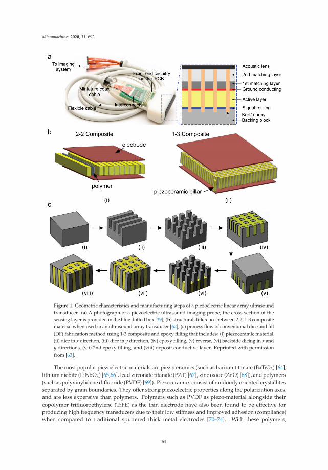
Micromachines 2020, 11, 692
Figure 1. Geometric characteristics and manufacturing steps of a piezoelectric linear array ultrasoundtransducer. (a) A photograph of a piezoelectric ultrasound imaging probe; the cross-section of thesensing layer is provided in the blue dotted box [39], (b) structural difference between 2-2, 1-3 compositematerial when used in an ultrasound array transducer [62], (c) process flow of conventional dice and fill(DF) fabrication method using 1-3 composite and epoxy filling that includes: (i) piezoceramic material,(ii) dice in x direction, (iii) dice in y direction, (iv) epoxy filling, (v) reverse, (vi) backside dicing in x andy directions, (vii) 2nd epoxy filling, and (viii) deposit conductive layer. Reprinted with permissionfrom [63].
The most popular piezoelectric materials are piezoceramics (such as barium titanate (BaTiO3) [64],lithium niobite (LiNbO3) [65,66], lead zirconate titanate (PZT) [67], zinc oxide (ZnO) [68]), and polymers(such as polyvinylidene difluoride (PVDF) [69]). Piezoceramics consist of randomly oriented crystallitesseparated by grain boundaries. They offer strong piezoelectric properties along the polarization axes,and are less expensive than polymers. Polymers such as PVDF as piezo-material alongside theircopolymer trifluoroethylene (TrFE) as the thin electrode have also been found to be effective forproducing high frequency transducers due to their low stiffness and improved adhesion (compliance)when compared to traditional sputtered thick metal electrodes [70–74]. With these polymers,
64
Micromachines 2020, 11, 692
low acoustic impedance (i.e., close to the tissue impedance) can be achieved at the cost of lowenergy conversion. To further improve the quality of piezoelectric transducers, composite materialshave been developed [75]. The piezoelectric composite consists of a piezoelectric phase (piezo-ceramic)and a polymer phase (epoxy resin), with a certain connection mode, a certain volume or mass ratio,and a certain spatial geometric distribution [76]. Among different materials, PZT-epoxy resin-basedcomposites have been the dominant material to realize the active elements of transducers in piezoelectrictransducers [77–80]. Piezo-composites are classified according to respective phase connectivity (0, 1, 2,or 3) through which the phase is continuous. Since, there are two phases in piezo-composites they arereferred by 2-digit numbers [76]. The first digit references the piezoelectric phase and the second digitreferences the polymer phase. Out of 10 conventional different combinations of connectivity [81,82],piezoelectric 1–3 [9,13] and 2–2 [14] composites are commonly used in transducer technology and areproven to exhibit high coupling coefficient with low-acoustic impedance and low stiffness, leadingto improved sensitivity compared to monolithic piezo-materials [62,83]. Structural schematics of1-3 and 2-2 piezo-composites are shown in Figure 1b. The composites are limited to low energyand low temperature applications due to their inherently low mechanical quality factor and thermalconductivity. A quantitative comparison among different types of piezo-material in terms of theirdeterminant properties is provided in Table 1. Speed of sound (SOS) in biological tissues are in therange of 1450–1580 ms−1, thus it is desirable to choose a piezo-material with similar SOS. Table 1 showsthat piezo-composite materials provide acoustic impedance and SOS similar to those of biologicaltissues, with a higher coupling coefficient as compared to polymer or ceramic based piezo-materials;that justifies the use of composites as the preferred piezo layer in ultrasound transducers.
Table 1. Material properties of widely used piezoelectric materials in manufacturing of ultrasoundtransducers [65,66,76,84–86].
Piezo-materials Acoustic Impedance (MRayl) Coupling Coefficient Relative Permittivity Density (kg·m−3) Speed of Sound (m·s−1)
Quartz 13.3 0.093 4.5 2648 5000
LiNbO3 39 0.49 39 4700 7360
PZT 33.7 0.51 1470–1700 7500 4580
PMN-PT 37.1 0.58 680–800 8060 4610
PVDF 3.9 0.12–0.29 5–13 1780 2200
1-3 Composite 9 0.6 450 3673 1540
Piezoelectric transducers can be developed as single elements or aggregated into an array(e.g., linear, convex, arc, ring, and spherical). A list of ultrasound transducer arrays that have beenused in different photoacoustic imaging applications is given in Table 2. Conventionally, the arrays arerealized through dice and fill method (DF) [75]. The DF method involves making a series of parallel cutson a piece of bulk piezoelectric material with a mechanical dicing saw (Figure 1c shows the steps of aconventional DF fabrication method using 1-3 composite and epoxy filling). The material is then dicedin the perpendicular direction to produce posts with a rectangular cross section. The diced material isbackfilled with a polymer, then the base ceramic support is removed by lapping polishing [62,63,76].For 2-2 composite, step 3 is skipped and the remaining steps are similar to those for 1-3 composite.Other alternative methods to make piezoelectric transducers include the interdigital bonding technique,stacked plates or lamination techniques, fiber processing, and laser machining [75].
65
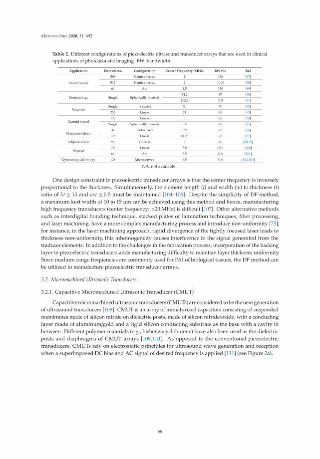
Micromachines 2020, 11, 692
Table 2. Different configurations of piezoelectric ultrasound transducer arrays that are used in clinicalapplications of photoacoustic imaging. BW: bandwidth.
Application Element no. Configuration Center Frequency (MHz) BW (%) Ref
Breast cancer
588 Hemispherical 1 130 [87]
512 Hemispherical 2 >100 [88]
64 Arc 1.5 130 [89]
Dermatology Single Spherically focused54.2 97 [90]
102.8 105 [91]
VascularSingle Focused 50 70 [92]
256 Linear 21 66 [93]
Carotid vessel128 Linear 5 80 [94]
Single Spherically focused 100 80 [95]
Musculoskeletal32 Unfocused 6.25 80 [96]
128 Linear 11.25 75 [97]
Adipose tissue 256 Curved 5 60 [98,99]
Thyroid192 Linear 5.8 82.7 [100]
64 Arc 7.5 NA [101]
Gynecology &Urology 128 Microconvex 6.5 NA [102,103]
NA: not available.
One design constraint in piezoelectric transducer arrays is that the center frequency is inverselyproportional to the thickness. Simultaneously, the element length (l) and width (w) to thickness (t)ratio of l:t ≥ 10 and w:t ≤ 0.5 must be maintained [104–106]. Despite the simplicity of DF method,a maximum kerf width of 10 to 15 μm can be achieved using this method and hence, manufacturinghigh frequency transducers (center frequency: >20 MHz) is difficult [107]. Other alternative methodssuch as interdigital bonding technique, stacked plates or lamination techniques, fiber processing,and laser machining, have a more complex manufacturing process and introduce non-uniformity [75];for instance, in the laser machining approach, rapid divergence of the tightly focused laser leads tothickness non-uniformity, this inhomogeneity causes interference in the signal generated from thetraducer elements. In addition to the challenges in the fabrication process, incorporation of the backinglayer in piezoelectric transducers adds manufacturing difficulty to maintain layer thickness uniformity.Since medium range frequencies are commonly used for PAI of biological tissues, the DF method canbe utilized to manufacture piezoelectric transducer arrays.
3.2. Micromachined Ultrasonic Transducers
3.2.1. Capacitive Micromachined Ultrasonic Transducer (CMUT)
Capacitive micromachined ultrasonic transducers (CMUTs) are considered to be the next generationof ultrasound transducers [108]. CMUT is an array of miniaturized capacitors consisting of suspendedmembranes made of silicon nitride on dielectric posts, made of silicon nitride/oxide, with a conductinglayer made of aluminum/gold and a rigid silicon conducting substrate as the base with a cavity inbetween. Different polymer materials (e.g., bisbenzocyclobutene) have also been used as the dielectricposts and diaphragms of CMUT arrays [109,110]. As opposed to the conventional piezoelectrictransducers, CMUTs rely on electrostatic principles for ultrasound wave generation and receptionwhen a superimposed DC bias and AC signal of desired frequency is applied [111] (see Figure 2a).
66
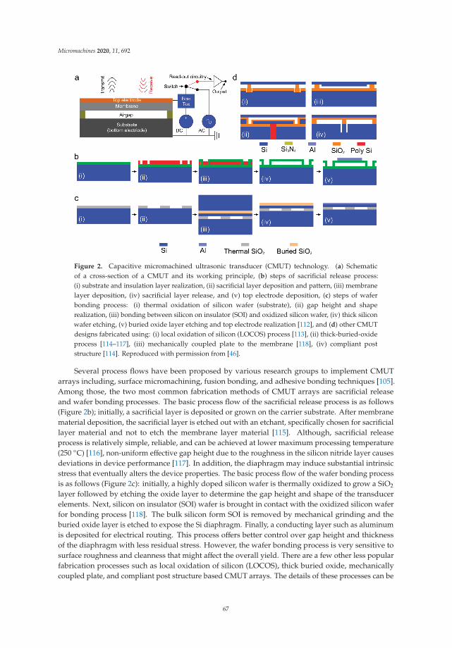
Micromachines 2020, 11, 692
Figure 2. Capacitive micromachined ultrasonic transducer (CMUT) technology. (a) Schematicof a cross-section of a CMUT and its working principle, (b) steps of sacrificial release process:(i) substrate and insulation layer realization, (ii) sacrificial layer deposition and pattern, (iii) membranelayer deposition, (iv) sacrificial layer release, and (v) top electrode deposition, (c) steps of waferbonding process: (i) thermal oxidation of silicon wafer (substrate), (ii) gap height and shaperealization, (iii) bonding between silicon on insulator (SOI) and oxidized silicon wafer, (iv) thick siliconwafer etching, (v) buried oxide layer etching and top electrode realization [112], and (d) other CMUTdesigns fabricated using: (i) local oxidation of silicon (LOCOS) process [113], (ii) thick-buried-oxideprocess [114–117], (iii) mechanically coupled plate to the membrane [118], (iv) compliant poststructure [114]. Reproduced with permission from [46].
Several process flows have been proposed by various research groups to implement CMUTarrays including, surface micromachining, fusion bonding, and adhesive bonding techniques [105].Among those, the two most common fabrication methods of CMUT arrays are sacrificial releaseand wafer bonding processes. The basic process flow of the sacrificial release process is as follows(Figure 2b); initially, a sacrificial layer is deposited or grown on the carrier substrate. After membranematerial deposition, the sacrificial layer is etched out with an etchant, specifically chosen for sacrificiallayer material and not to etch the membrane layer material [115]. Although, sacrificial releaseprocess is relatively simple, reliable, and can be achieved at lower maximum processing temperature(250 ◦C) [116], non-uniform effective gap height due to the roughness in the silicon nitride layer causesdeviations in device performance [117]. In addition, the diaphragm may induce substantial intrinsicstress that eventually alters the device properties. The basic process flow of the wafer bonding processis as follows (Figure 2c): initially, a highly doped silicon wafer is thermally oxidized to grow a SiO2
layer followed by etching the oxide layer to determine the gap height and shape of the transducerelements. Next, silicon on insulator (SOI) wafer is brought in contact with the oxidized silicon waferfor bonding process [118]. The bulk silicon form SOI is removed by mechanical grinding and theburied oxide layer is etched to expose the Si diaphragm. Finally, a conducting layer such as aluminumis deposited for electrical routing. This process offers better control over gap height and thicknessof the diaphragm with less residual stress. However, the wafer bonding process is very sensitive tosurface roughness and cleanness that might affect the overall yield. There are a few other less popularfabrication processes such as local oxidation of silicon (LOCOS), thick buried oxide, mechanicallycoupled plate, and compliant post structure based CMUT arrays. The details of these processes can be
67
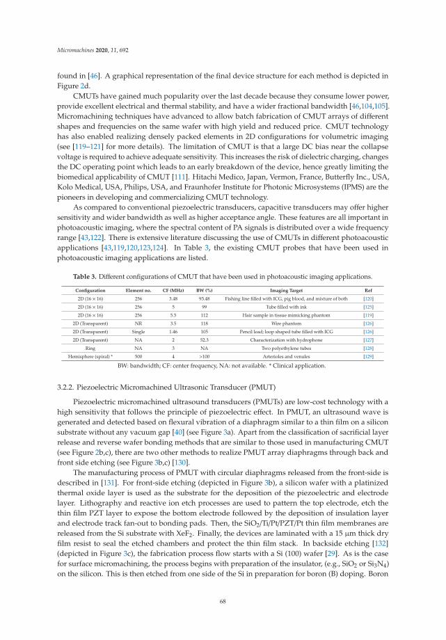
Micromachines 2020, 11, 692
found in [46]. A graphical representation of the final device structure for each method is depicted inFigure 2d.
CMUTs have gained much popularity over the last decade because they consume lower power,provide excellent electrical and thermal stability, and have a wider fractional bandwidth [46,104,105].Micromachining techniques have advanced to allow batch fabrication of CMUT arrays of differentshapes and frequencies on the same wafer with high yield and reduced price. CMUT technologyhas also enabled realizing densely packed elements in 2D configurations for volumetric imaging(see [119–121] for more details). The limitation of CMUT is that a large DC bias near the collapsevoltage is required to achieve adequate sensitivity. This increases the risk of dielectric charging, changesthe DC operating point which leads to an early breakdown of the device, hence greatly limiting thebiomedical applicability of CMUT [111]. Hitachi Medico, Japan, Vermon, France, Butterfly Inc., USA,Kolo Medical, USA, Philips, USA, and Fraunhofer Institute for Photonic Microsystems (IPMS) are thepioneers in developing and commercializing CMUT technology.
As compared to conventional piezoelectric transducers, capacitive transducers may offer highersensitivity and wider bandwidth as well as higher acceptance angle. These features are all important inphotoacoustic imaging, where the spectral content of PA signals is distributed over a wide frequencyrange [43,122]. There is extensive literature discussing the use of CMUTs in different photoacousticapplications [43,119,120,123,124]. In Table 3, the existing CMUT probes that have been used inphotoacoustic imaging applications are listed.
Table 3. Different configurations of CMUT that have been used in photoacoustic imaging applications.
Configuration Element no. CF (MHz) BW (%) Imaging Target Ref
2D (16 × 16) 256 3.48 93.48 Fishing line filled with ICG, pig blood, and mixture of both [120]
2D (16 × 16) 256 5 99 Tube filled with ink [125]
2D (16 × 16) 256 5.5 112 Hair sample in tissue mimicking phantom [119]
2D (Transparent) NR 3.5 118 Wire phantom [126]
2D (Transparent) Single 1.46 105 Pencil lead; loop shaped tube filled with ICG [126]
2D (Transparent) NA 2 52.3 Characterization with hydrophone [127]
Ring NA 3 NA Two polyethylene tubes [128]
Hemisphere (spiral) * 500 4 >100 Arterioles and venules [129]
BW: bandwidth; CF: center frequency, NA: not available. * Clinical application.
3.2.2. Piezoelectric Micromachined Ultrasonic Transducer (PMUT)
Piezoelectric micromachined ultrasound transducers (PMUTs) are low-cost technology with ahigh sensitivity that follows the principle of piezoelectric effect. In PMUT, an ultrasound wave isgenerated and detected based on flexural vibration of a diaphragm similar to a thin film on a siliconsubstrate without any vacuum gap [40] (see Figure 3a). Apart from the classification of sacrificial layerrelease and reverse wafer bonding methods that are similar to those used in manufacturing CMUT(see Figure 2b,c), there are two other methods to realize PMUT array diaphragms through back andfront side etching (see Figure 3b,c) [130].
The manufacturing process of PMUT with circular diaphragms released from the front-side isdescribed in [131]. For front-side etching (depicted in Figure 3b), a silicon wafer with a platinizedthermal oxide layer is used as the substrate for the deposition of the piezoelectric and electrodelayer. Lithography and reactive ion etch processes are used to pattern the top electrode, etch thethin film PZT layer to expose the bottom electrode followed by the deposition of insulation layerand electrode track fan-out to bonding pads. Then, the SiO2/Ti/Pt/PZT/Pt thin film membranes arereleased from the Si substrate with XeF2. Finally, the devices are laminated with a 15 μm thick dryfilm resist to seal the etched chambers and protect the thin film stack. In backside etching [132](depicted in Figure 3c), the fabrication process flow starts with a Si (100) wafer [29]. As is the casefor surface micromachining, the process begins with preparation of the insulator, (e.g., SiO2 or Si3N4)on the silicon. This is then etched from one side of the Si in preparation for boron (B) doping. Boron
68
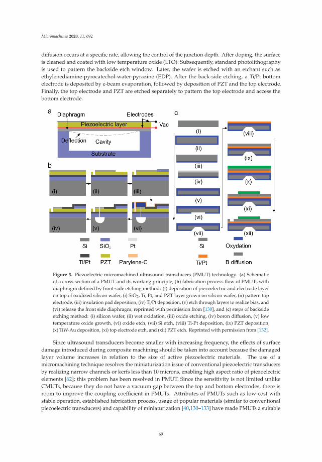
Micromachines 2020, 11, 692
diffusion occurs at a specific rate, allowing the control of the junction depth. After doping, the surfaceis cleaned and coated with low temperature oxide (LTO). Subsequently, standard photolithographyis used to pattern the backside etch window. Later, the wafer is etched with an etchant such asethylenediamine-pyrocatechol-water-pyrazine (EDP). After the back-side etching, a Ti/Pt bottomelectrode is deposited by e-beam evaporation, followed by deposition of PZT and the top electrode.Finally, the top electrode and PZT are etched separately to pattern the top electrode and access thebottom electrode.
Figure 3. Piezoelectric micromachined ultrasound transducers (PMUT) technology. (a) Schematicof a cross-section of a PMUT and its working principle, (b) fabrication process flow of PMUTs withdiaphragm defined by front-side etching method: (i) deposition of piezoelectric and electrode layeron top of oxidized silicon wafer, (i) SiO2, Ti, Pt, and PZT layer grown on silicon wafer, (ii) pattern topelectrode, (iii) insulation pad deposition, (iv) Ti/Pt deposition, (v) etch through layers to realize bias, and(vi) release the front side diaphragm, reprinted with permission from [130], and (c) steps of backsideetching method: (i) silicon wafer, (ii) wet oxidation, (iii) oxide etching, (iv) boron diffusion, (v) lowtemperature oxide growth, (vi) oxide etch, (vii) Si etch, (viii) Ti-Pt deposition, (ix) PZT deposition,(x) TiW-Au deposition, (xi) top electrode etch, and (xii) PZT etch. Reprinted with permission from [132].
Since ultrasound transducers become smaller with increasing frequency, the effects of surfacedamage introduced during composite machining should be taken into account because the damagedlayer volume increases in relation to the size of active piezoelectric materials. The use of amicromachining technique resolves the miniaturization issue of conventional piezoelectric transducersby realizing narrow channels or kerfs less than 10 microns, enabling high aspect ratio of piezoelectricelements [62]; this problem has been resolved in PMUT. Since the sensitivity is not limited unlikeCMUTs, because they do not have a vacuum gap between the top and bottom electrodes, there isroom to improve the coupling coefficient in PMUTs. Attributes of PMUTs such as low-cost withstable operation, established fabrication process, usage of popular materials (similar to conventionalpiezoelectric transducers) and capability of miniaturization [40,130–133] have made PMUTs a suitable
69
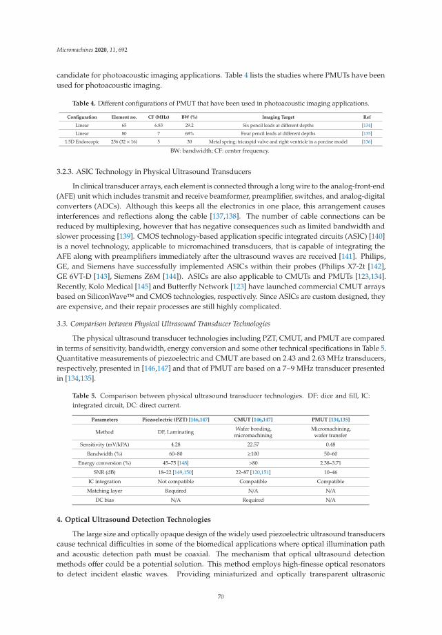
Micromachines 2020, 11, 692
candidate for photoacoustic imaging applications. Table 4 lists the studies where PMUTs have beenused for photoacoustic imaging.
Table 4. Different configurations of PMUT that have been used in photoacoustic imaging applications.
Configuration Element no. CF (MHz) BW (%) Imaging Target Ref
Linear 65 6.83 29.2 Six pencil leads at different depths [134]
Linear 80 7 68% Four pencil leads at different depths [135]
1.5D Endoscopic 256 (32 × 16) 5 30 Metal spring; tricuspid valve and right ventricle in a porcine model [136]
BW: bandwidth; CF: center frequency.
3.2.3. ASIC Technology in Physical Ultrasound Transducers
In clinical transducer arrays, each element is connected through a long wire to the analog-front-end(AFE) unit which includes transmit and receive beamformer, preamplifier, switches, and analog-digitalconverters (ADCs). Although this keeps all the electronics in one place, this arrangement causesinterferences and reflections along the cable [137,138]. The number of cable connections can bereduced by multiplexing, however that has negative consequences such as limited bandwidth andslower processing [139]. CMOS technology-based application specific integrated circuits (ASIC) [140]is a novel technology, applicable to micromachined transducers, that is capable of integrating theAFE along with preamplifiers immediately after the ultrasound waves are received [141]. Philips,GE, and Siemens have successfully implemented ASICs within their probes (Philips X7-2t [142],GE 6VT-D [143], Siemens Z6M [144]). ASICs are also applicable to CMUTs and PMUTs [123,134].Recently, Kolo Medical [145] and Butterfly Network [123] have launched commercial CMUT arraysbased on SiliconWave™ and CMOS technologies, respectively. Since ASICs are custom designed, theyare expensive, and their repair processes are still highly complicated.
3.3. Comparison between Physical Ultrasound Transducer Technologies
The physical ultrasound transducer technologies including PZT, CMUT, and PMUT are comparedin terms of sensitivity, bandwidth, energy conversion and some other technical specifications in Table 5.Quantitative measurements of piezoelectric and CMUT are based on 2.43 and 2.63 MHz transducers,respectively, presented in [146,147] and that of PMUT are based on a 7~9 MHz transducer presentedin [134,135].
Table 5. Comparison between physical ultrasound transducer technologies. DF: dice and fill, IC:integrated circuit, DC: direct current.
Parameters Piezoelectric (PZT) [146,147] CMUT [146,147] PMUT [134,135]
Method DF, Laminating Wafer bonding,micromachining
Micromachining,wafer transfer
Sensitivity (mV/kPA) 4.28 22.57 0.48
Bandwidth (%) 60–80 ≥100 50–60
Energy conversion (%) 45–75 [148] >80 2.38–3.71
SNR (dB) 18–22 [149,150] 22–87 [120,151] 10–46
IC integration Not compatible Compatible Compatible
Matching layer Required N/A N/A
DC bias N/A Required N/A
4. Optical Ultrasound Detection Technologies
The large size and optically opaque design of the widely used piezoelectric ultrasound transducerscause technical difficulties in some of the biomedical applications where optical illumination pathand acoustic detection path must be coaxial. The mechanism that optical ultrasound detectionmethods offer could be a potential solution. This method employs high-finesse optical resonatorsto detect incident elastic waves. Providing miniaturized and optically transparent ultrasonic
70
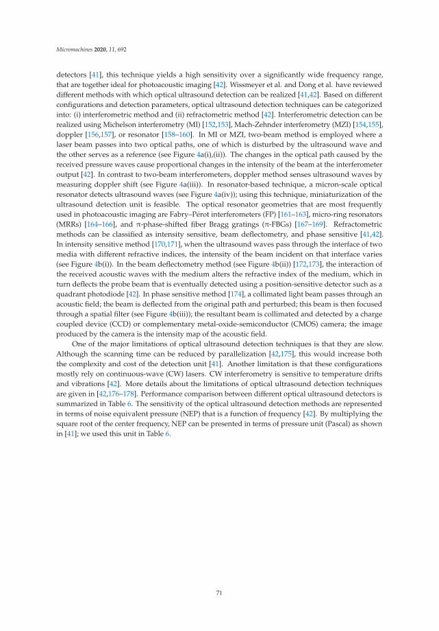
Micromachines 2020, 11, 692
detectors [41], this technique yields a high sensitivity over a significantly wide frequency range,that are together ideal for photoacoustic imaging [42]. Wissmeyer et al. and Dong et al. have revieweddifferent methods with which optical ultrasound detection can be realized [41,42]. Based on differentconfigurations and detection parameters, optical ultrasound detection techniques can be categorizedinto: (i) interferometric method and (ii) refractometric method [42]. Interferometric detection can berealized using Michelson interferometry (MI) [152,153], Mach-Zehnder interferometry (MZI) [154,155],doppler [156,157], or resonator [158–160]. In MI or MZI, two-beam method is employed where alaser beam passes into two optical paths, one of which is disturbed by the ultrasound wave andthe other serves as a reference (see Figure 4a(i),(ii)). The changes in the optical path caused by thereceived pressure waves cause proportional changes in the intensity of the beam at the interferometeroutput [42]. In contrast to two-beam interferometers, doppler method senses ultrasound waves bymeasuring doppler shift (see Figure 4a(iii)). In resonator-based technique, a micron-scale opticalresonator detects ultrasound waves (see Figure 4a(iv)); using this technique, miniaturization of theultrasound detection unit is feasible. The optical resonator geometries that are most frequentlyused in photoacoustic imaging are Fabry–Pérot interferometers (FP) [161–163], micro-ring resonators(MRRs) [164–166], and π-phase-shifted fiber Bragg gratings (π-FBGs) [167–169]. Refractometricmethods can be classified as intensity sensitive, beam deflectometry, and phase sensitive [41,42].In intensity sensitive method [170,171], when the ultrasound waves pass through the interface of twomedia with different refractive indices, the intensity of the beam incident on that interface varies(see Figure 4b(i)). In the beam deflectometry method (see Figure 4b(ii)) [172,173], the interaction ofthe received acoustic waves with the medium alters the refractive index of the medium, which inturn deflects the probe beam that is eventually detected using a position-sensitive detector such as aquadrant photodiode [42]. In phase sensitive method [174], a collimated light beam passes through anacoustic field; the beam is deflected from the original path and perturbed; this beam is then focusedthrough a spatial filter (see Figure 4b(iii)); the resultant beam is collimated and detected by a chargecoupled device (CCD) or complementary metal-oxide-semiconductor (CMOS) camera; the imageproduced by the camera is the intensity map of the acoustic field.
One of the major limitations of optical ultrasound detection techniques is that they are slow.Although the scanning time can be reduced by parallelization [42,175], this would increase boththe complexity and cost of the detection unit [41]. Another limitation is that these configurationsmostly rely on continuous-wave (CW) lasers. CW interferometry is sensitive to temperature driftsand vibrations [42]. More details about the limitations of optical ultrasound detection techniquesare given in [42,176–178]. Performance comparison between different optical ultrasound detectors issummarized in Table 6. The sensitivity of the optical ultrasound detection methods are representedin terms of noise equivalent pressure (NEP) that is a function of frequency [42]. By multiplying thesquare root of the center frequency, NEP can be presented in terms of pressure unit (Pascal) as shownin [41]; we used this unit in Table 6.
71
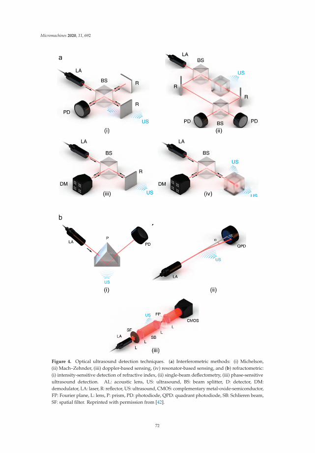
Micromachines 2020, 11, 692
Figure 4. Optical ultrasound detection techniques. (a) Interferometric methods: (i) Michelson,(ii) Mach–Zehnder, (iii) doppler-based sensing, (iv) resonator-based sensing, and (b) refractometric:(i) intensity-sensitive detection of refractive index, (ii) single-beam deflectometry, (iii) phase-sensitiveultrasound detection. AL: acoustic lens, US: ultrasound, BS: beam splitter, D: detector, DM:demodulator, LA: laser, R: reflector, US: ultrasound, CMOS: complementary metal-oxide-semiconductor,FP: Fourier plane, L: lens, P: prism, PD: photodiode, QPD: quadrant photodiode, SB: Schlieren beam,SF: spatial filter. Reprinted with permission from [42].
72
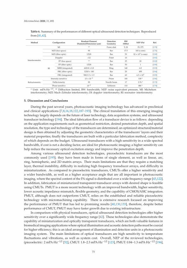
Micromachines 2020, 11, 692
Table 6. Summary of the performances of different optical ultrasound detection techniques. Reproducedfrom [41,42].
Method ConfigurationReadout Element
Diameter/Dimension (μm)DetectionGeometry
BW(MHz)
NEP (Pa) Ref.
Interferometric
MI ** Point; disk 5; 20 35; 275 [179]
MZI (free space) 90 Bar 17.5 100 (x mm) [176]
MZI (fiber optic) 125/8 Bar 50 92 × 103 (x mm) [180]
Doppler -/12 Point 10 - [181]
RI
FP (free space) ** Bar 25 20 [182]
FP (fiber optic) 125/8 Bar 50 1 [180]
MRR (integrated) 60/0.8 × 0.8 Ring 140 6.8 [183]
FBG (fiber optic) 125/8 × 100 Bar 20 450 [184]
FBG (integrated) 500/1.5 × 1.5 Bar 60 6.5 × 10³ [185]
Refractometric
Intensity-sensitive 15 × 10−3 Prism 100 100 * [186]
Deflectometry 90 Needle beam 17 2.76 * [172]
Phase-sensitive 10−2 Schlieren 110 486 * [174]
* Unit: mPA·Hz−1/2, ** Diffraction limited, BW: bandwidth; NEP: noise equivalent pressure, MI: Michelsoninterferometry; MZI: Mach–Zehnder interferometry; DI: doppler- interferometry; RI: resonator- interferometry.
5. Discussion and Conclusions
During the past several years, photoacoustic imaging technology has advanced in preclinicaland clinical applications [7,8,16,18,122,187–193]. The clinical translation of this emerging imagingtechnology largely depends on the future of laser technology, data acquisition systems, and ultrasoundtransducer technology [194]. The ideal fabrication flow of a transducer device is as follows: dependingon the application requirements such as geometrical restriction, desired penetration depth, and spatialresolution, the type and technology of the transducers are determined; an optimized structural/materialdesign is then obtained by adjusting the geometric characteristics of the transducers’ layers and theirmaterial properties; finally the transducers are built with a particular fabrication method, complexityof which depends on the budget. Ultrasound transducers with a high sensitivity in a wide spectralbandwidth, if cost is not a deciding factor, are ideal for photoacoustic imaging; a higher sensitivity canhelp reduce the necessary optical excitation energy and improve the penetration depth.
Among various ultrasound detection technologies, piezoelectric transducers are the mostcommonly used [195]; they have been made in forms of single element, as well as linear, arc,ring, hemispheric, and 2D matrix arrays. Their main limitations are that they require a matchinglayer, thermal instability, difficulty in realizing high frequency transducer arrays, and difficulty inminiaturization. As compared to piezoelectric transducers, CMUTs offer a higher sensitivity anda wider bandwidth, as well as a higher acceptance angle that are all important in photoacousticimaging, where the spectral content of the PA signal is distributed over a wide frequency range [43,122].In addition, fabrication of miniaturized transparent transducer arrays with desired shape is feasibleusing CMUTs. PMUT is a more recent technology with an improved bandwidth, higher sensitivity,lower acoustic impedance mismatch, flexible geometry, and the capability of CMOS/ASIC integration.PMUT, although does not outperform CMUT, relies on the established and reliable piezoelectrictechnology with micromachining capability. There is extensive research focused on improvingthe performance of PMUT that has led to promising results [40,130,133], therefore, despite betterperformance of CMUT, PMUT may have faster growth due to existing infrastructure.
In comparison with physical transducers, optical ultrasound detection technologies offer highersensitivity over a significantly wide frequency range [42]. These technologies also demonstrate thecapability of miniaturization and optically transparent transducers, which are both valuable features inbiomedical imaging applications where optical illumination and acoustic detection paths must be coaxialfor higher efficiency; this is an ideal arrangement of illumination and detection units in a photoacousticimaging system. The main limitations of optical transducers are high sensitivity to temperaturefluctuations and vibrations, as well as system cost. Overall, NEP of the reviewed technologies,(piezoelectric: 2 mPA·Hz−1/2 [52], CMUT: 1.8~2.3 mPA·Hz−1/2 [123], PMUT: 0.84~1.3 mPA·Hz−1/2 [196],
73
Micromachines 2020, 11, 692
optical ultrasound detection: 0.45~486 mPA·Hz−1/2 [42]) suggest that micromachined transducers(i.e., CMUTs and PMUTs) may be the more suitable transducers for photoacoustic imaging applications.
ASIC is a complimentary technology in transducer manufacturing to integrate the analog-front-endwithin the probe housing in order to reduce the noise of the transducer signal. ASIC improves the overallperformance of existing transducers and therefore could help in facilitating the clinical translation ofphotoacoustic imaging. According to the technology market analyst projection, the usage of ASICintegrated miniature ultrasound transducer probes based on micromachined technologies will see~18% annual compound growth rate by 2023 due to the advent of micromachining processes [197].With the fast-growing ultrasound transducer technology, numerous computational methods have alsobeen studied to further improve the performance of transducers by reducing noise in the transducersignal [198,199]; the result has been higher quality images [5,200,201]. With the advancement ofultrasound technology, more biomedical applications, which are currently performed using opticaltechnologies, can be realized [12,202–208].
Author Contributions: Conceptualization, R.M. and K.A.; Methodology, K.A.; Software, R.M.; Validation, R.M.,K.K., and K.A.; Formal Analysis, R.M. and K.A.; Investigation, R.M. and K.A.; Resources, K.A.; Writing-OriginalDraft Preparation, R.M.; Writing-Review & Editing, R.M., K.K., and K.A.; Visualization, R.M.; Supervision, K.A.;Funding Acquisition, K.A. All authors have read and agreed to the published version of the manuscript.
Funding: This work was supported by the National Institutes of Health R01EB027769-01 and R01EB028661-01.
Conflicts of Interest: The authors declare no conflict of interest.
References
1. Dance, D.R.; Christofides, S.; Maidment, A.; McLean, I.; Ng, K. Diagnostic Radiology Physics: A Handbook forTeachers and Students. Endorsed by: American Association of Physicists in Medicine, Asia-Oceania Federation ofOrganizations for Medical Physics, European Federation of Organisations for Medical Physics; International AtomicEnergy Agency (IAEA): Vienna, Austria, 2014.
2. Wang, L.V. Tutorial on photoacoustic microscopy and computed tomography. IEEE J. Sel. Top.Quantum Electron. 2008, 14, 171–179. [CrossRef]
3. Wang, L.V.; Hu, S. Photoacoustic tomography: In vivo imaging from organelles to organs. Science 2012, 335,1458–1462. [CrossRef] [PubMed]
4. Xia, J.; Yao, J.; Wang, L.V. Photoacoustic tomography: Principles and advances. Electromagn. Waves (Camb.)2014, 147, 1–22. [CrossRef] [PubMed]
5. Yao, J.; Wang, L.V. Photoacoustic microscopy. Laser Photonics Rev. 2013, 7, 758–778. [CrossRef] [PubMed]6. Zhou, Y.; Yao, J.; Wang, L.V. Tutorial on photoacoustic tomography. J. Biomed. Opt. 2016, 21, 061007.
[CrossRef]7. Manwar, R.; Hosseinzadeh, M.; Hariri, A.; Kratkiewicz, K.; Noei, S.; Avanaki, M.N. Photoacoustic signal
enhancement: Towards Utilization of low energy laser diodes in real-time photoacoustic imaging. Sensors2018, 18, 3498. [CrossRef]
8. Zafar, M.; Kratkiewicz, K.; Manwar, R.; Avanaki, M. Development of low-cost fast photoacoustic computedtomography: System characterization and phantom study. Appl. Sci. 2019, 9, 374. [CrossRef]
9. Fatima, A.; Kratkiewicz, K.; Manwar, R.; Zafar, M.; Zhang, R.; Huang, B.; Dadashzadesh, N.; Xia, J.;Avanaki, M. Review of cost reduction methods in photoacoustic computed tomography. Photoacoustics 2019,15, 100137. [CrossRef]
10. Wang, L.V. Photoacoustic Imaging and Spectroscopy; CRC Press: Boca Raton, FL, USA, 2009.11. Wang, L.V.; Yao, J. A practical guide to photoacoustic tomography in the life sciences. Nat. Methods 2016,
13, 627. [CrossRef]12. Turani, Z.; Fatemizadeh, E.; Blumetti, T.; Daveluy, S.; Moraes, A.F.; Chen, W.; Mehregan, D.; Andersen, P.E.;
Nasiriavanaki, M. Optical radiomic signatures derived from optical coherence tomography images improveidentification of melanoma. Cancer Res. 2019, 79, 2021–2030. [CrossRef]
13. Rayyan, A.; Karl, K.; Mohammad, R.N.A. Photoacoustic imaging: A promising alternative to transcranialultrasound. Editor. Res. J. Photonics 2018, 2, 411–420.
74
Micromachines 2020, 11, 692
14. Zafar, M.; Kratkiewicz, K.; Manwar, R.; Avanaki, M. Low-cost fast photoacoustic computed tomography:Phantom study. In Proceedings of the Photons Plus Ultrasound: Imaging and Sensing 2019, San Francisco,CA, USA, 3–6 February 2019.
15. Mozaffarzadeh, M.; Mahloojifar, A.; Orooji, M.; Adabi, S.; Nasiriavanaki, M. Double-stage delay multiply andsum beamforming algorithm: Application to linear-array photoacoustic imaging. IEEE Trans. Biomed. Eng.2018, 65, 31–42. [CrossRef]
16. Mozaffarzadeh, M.; Mahloojifar, A.; Orooji, M.; Kratkiewicz, K.; Adabi, S.; Nasiriavanaki, M. Linear-arrayphotoacoustic imaging using minimum variance-based delay multiply and sum adaptive beamformingalgorithm. J. Biomed. Opt. 2018, 23, 026002. [CrossRef] [PubMed]
17. Omidi, P.; Zafar, M.; Mozaffarzadeh, M.; Hariri, A.; Haung, X.; Orooji, M.; Nasiriavanaki, M. A noveldictionary-based image reconstruction for photoacoustic computed tomography. Appl. Sci. 2018, 8, 1570.[CrossRef]
18. Nasiriavanaki, M.; Xia, J.; Wan, H.; Bauer, A.Q.; Culver, J.P.; Wang, L.V. High-resolution photoacoustictomography of resting-state functional connectivity in the mouse brain. Proc. Natl. Acad. Sci. USA 2014, 111,21–26. [CrossRef] [PubMed]
19. Upputuri, P.K.; Periyasamy, V.; Kalva, S.K.; Pramanik, M. A High-performance Compact PhotoacousticTomography System for In Vivo Small-animal Brain Imaging. J. Vis. Exp. 2017, 124, e55811. [CrossRef]
20. Xia, J.; Wang, L.V. Small-Animal Whole-Body Photoacoustic Tomography: A Review. IEEE Trans. Biomed. Eng.2014, 61, 1380–1389. [CrossRef] [PubMed]
21. Upputuri, P.K.; Pramanik, M. Dynamic in vivo imaging of small animal brain using pulsed laser diode-basedphotoacoustic tomography system. J. Biomed. Opt. 2017, 22, 1. [CrossRef] [PubMed]
22. Upputuri, P.K.; Pramanik, M. Photoacoustic imaging in the second near-infrared window: A review.J. Biomed. Opt. 2019, 24, 1–20. [CrossRef]
23. Liu, W.; Zhang, H.F. Photoacoustic imaging of the eye: A mini review. Photoacoustics 2016, 4, 112–123.[CrossRef]
24. Silverman, R.H.; Kong, F.; Chen, Y.; Lloyd, H.O.; Kim, H.H.; Cannata, J.M.; Shung, K.K.; Coleman, D.J.High-Resolution Photoacoustic Imaging of Ocular Tissues. Ultrasound Med. Boil. 2010, 36, 733–742. [CrossRef][PubMed]
25. Nguyen, V.P.; Paulus, Y.M. Photoacoustic Ophthalmoscopy: Principle, Application, and Future Directions.J. Imaging 2018, 4, 149. [CrossRef] [PubMed]
26. Jeon, S.; Song, H.B.; Kim, J.; Lee, B.J.; Managuli, R.; Kim, J.H.; Kim, J.H.; Kim, C. In Vivo PhotoacousticImaging of Anterior Ocular Vasculature: A Random Sample Consensus Approach. Sci. Rep. 2017, 7, 4318.[CrossRef]
27. Wang, S.; Lin, J.; Wang, T.; Chen, X.; Huang, P. Recent Advances in Photoacoustic Imaging for Deep-TissueBiomedical Applications. Theranostics 2016, 6, 2394–2413. [CrossRef]
28. Mehrmohammadi, M.; Yoon, S.J.; Yeager, D.; Emelianov, S.Y. Photoacoustic Imaging for Cancer Detectionand Staging. Curr. Mol. Imaging 2013, 2, 89–105. [CrossRef] [PubMed]
29. Oh, J.-T.; Li, M.-L.; Zhang, H.F.; Maslov, K.; Stoica, G.; Wang, L.V. Three-dimensional imaging of skinmelanoma in vivo by dual-wavelength photoacoustic microscopy. J. Biomed. Opt. 2006, 11, 034032.[CrossRef]
30. Rao, A.P.; Bokde, N.D.; Sinha, S. Photoacoustic Imaging for Management of Breast Cancer: A LiteratureReview and Future Perspectives. Appl. Sci. 2020, 10, 767. [CrossRef]
31. Steinberg, I.; Huland, D.M.; Vermesh, O.; Frostig, H.E.; Tummers, W.S.; Gambhir, S.S. Photoacoustic clinicalimaging. Photoacoustics 2019, 14, 77–98. [CrossRef]
32. Fakhrejahani, E.; Torii, M.; Kitai, T.; Kanao, S.; Asao, Y.; Hashizume, Y.; Mikami, Y.; Yamaga, I.; Kataoka, M.;Sugie, T.; et al. Clinical Report on the First Prototype of a Photoacoustic Tomography System with DualIllumination for Breast Cancer Imaging. PLoS ONE 2015, 10, e0139113. [CrossRef]
33. Brown, E.; Brunker, J.; Bohndiek, S. Photoacoustic imaging as a tool to probe the tumour microenvironment.Dis. Model. Mech. 2019, 12, dmm039636. [CrossRef]
34. Valluru, K.S.; Willmann, J.K. Clinical photoacoustic imaging of cancer. Ultrason. 2016, 35, 267–280. [CrossRef][PubMed]
75

Micromachines 2020, 11, 692
35. Zhang, C.; Zhang, Y.; Hong, K.; Zhu, S.; Wan, J. Photoacoustic and fluorescence imaging of cutaneoussquamous cell carcinoma in living subjects using a probe targeting integrin αvβ6. Sci. Rep. 2017, 7, 42442.[CrossRef]
36. Zhang, E.Z.; Považay, B.; Laufer, J.; Alex, A.; Hofer, B.; Pedley, B.; Glittenberg, C.; Treeby, B.; Cox, B.T.;Beard, P.; et al. Multimodal photoacoustic and optical coherence tomography scanner using an all opticaldetection scheme for 3D morphological skin imaging. Biomed. Opt. Express 2011, 2, 2202–2215. [CrossRef][PubMed]
37. Guo, B.; Sheng, Z.; Hu, D.; Liu, C.; Wang, X.; Liu, B. Through Scalp and Skull NIR-II Photothermal Therapy ofDeep Orthotopic Brain Tumors with Precise Photoacoustic Imaging Guidance. Adv. Mater. 2018, 30, e1802591.[CrossRef] [PubMed]
38. Joshi, B.P.; Wang, T.D. Targeted Optical Imaging Agents in Cancer: Focus on Clinical Applications.Contrast Media Mol. Imaging 2018, 2018, 1–19. [CrossRef]
39. Lee, W.; Roh, Y. Ultrasonic transducers for medical diagnostic imaging. Biomed. Eng. Lett. 2017, 7, 91–97.[CrossRef]
40. Jung, J.; Lee, W.; Kang, W.; Shin, E.; Ryu, J.; Choi, H. Review of piezoelectric micromachined ultrasonictransducers and their applications. J. Micromech. Microeng. 2017, 27, 113001. [CrossRef]
41. Dong, B.; Sun, C.; Zhang, H.F. Optical detection of ultrasound in photoacoustic imaging. IEEE Trans.Biomed. Eng. 2017, 64, 4–15. [CrossRef]
42. Wissmeyer, G.; Pleitez, M.A.; Rosenthal, A.; Ntziachristos, V. Looking at sound: Optoacoustics with all-opticalultrasound detection. Light Sci. Appl. 2018, 7, 53. [CrossRef]
43. Vallet, M.; Varray, F.; Boutet, J.; Dinten, J.-M.; Caliano, G.; Savoia, A.S.; Vray, D. Quantitative comparison ofPZT and CMUT probes for photoacoustic imaging: Experimental validation. Photoacoustics 2017, 8, 48–58.[CrossRef]
44. Jiang, X.; Al-Jumaily, A.M. Ultrasound transducers for biomedical imaging and therapy. J. Eng. Sci. Med.Diagn. Ther. 2018, 1, 040201. [CrossRef]
45. Salim, M.S.; Abd Malek, M.F.; Heng, R.B.W.; Juni, K.M.; Sabri, N. Capacitive micromachined ultrasonictransducers: Technology and application. J. Med. Ultrasound 2012, 20, 8–31. [CrossRef]
46. Khuri-Yakub, B.T.; Oralkan, O. Capacitive micromachined ultrasonic transducers for medical imaging andtherapy. J. Micromech. Microeng. Struct. Devices Syst. 2011, 21, 54004–54014. [CrossRef] [PubMed]
47. Duy Le, A. Investigation of Element Variations in Ultrasound Transducer Arrays by Electrical ImpedanceMeasurements; Høgskolen i Sørøst-Norge: Notodden, Norway, 2016.
48. Yaralioglu, G.G.; Ergun, A.S.; Bayram, B.; Haeggstrom, E.; Khuri-Yakub, B.T. Calculation and measurementof electromechanical coupling coefficient of capacitive micromachined ultrasonic transducers. IEEE Trans.Ultrason. Ferroelectr. Freq. Control 2003, 50, 449–456. [CrossRef] [PubMed]
49. Yang, Y.; Wei, X.; Zhang, L.; Yao, W. The effect of electrical impedance matching on the electromechanicalcharacteristics of sandwiched piezoelectric ultrasonic transducers. Sensors 2017, 17, 2832. [CrossRef][PubMed]
50. Rathod, V.T. A review of electric impedance matching techniques for piezoelectric sensors, actuators andtransducers. Electronics 2019, 8, 169. [CrossRef]
51. Ritter, T.; Shung, K.; Hackenberger, W.; Wang, H.; Shrout, T.R. Performance of a high dielectric constantpiezoelectric ceramic for ultrasound transducers. In Proceedings of the 1999 IEEE Ultrasonics Symposium.Proceedings. International Symposium (Cat. No. 99CH37027), Caesars Tahoe, NV, USA, 17–20 October 1999.
52. Winkler, A.M.; Maslov, K.I.; Wang, L.V. Noise-equivalent sensitivity of photoacoustics. J. Biomed. Opt. 2013,18, 097003. [CrossRef]
53. Yao, J.; Wang, L.V. Sensitivity of photoacoustic microscopy. Photoacoustics 2014, 2, 87–101. [CrossRef]54. Zhou, Q.; Lam, K.H.; Zheng, H.; Qiu, W.; Shung, K.K. Piezoelectric single crystal ultrasonic transducers for
biomedical applications. Prog. Mater. Sci. 2014, 66, 87–111. [CrossRef] [PubMed]55. Szabo, T.L.; Lewin, P.A. Ultrasound transducer selection in clinical imaging practice. J. Ultrasound Med. 2013,
32, 573–582. [CrossRef]56. Zhang, J.X.J.; Hoshino, K. Molecular Sensors and Nanodevices: Principles, Designs and Applications in Biomedical
Engineering; Academic Press: Cambridge, MA, USA, 2018.57. Lerch, R. Finite element analysis of piezoelectric transducers. In Proceedings of the IEEE 1988 Ultrasonics
Symposium Proceedings, Chicago, IL, USA, 2–5 October 1988.
76
Micromachines 2020, 11, 692
58. Loveday, P.W. Analysis of piezoelectric ultrasonic transducers attached to waveguides using waveguidefinite elements. IEEE Trans. Ultrason. Ferroelectr. Freq. Control 2007, 54, 2045–2051. [CrossRef] [PubMed]
59. Hepher, M.J. Natural and synthetic piezoelectric materials for chemical sensors. In Proceedings of the 1992Sixth International Conference on Dielectric Materials, Measurements and Applications, Manchester, UK,7–10 September 1992.
60. Kumar, P.; Singh, S.; Thakur, O.P.; Prakash, C.; Goel, T.C. Study of lead magnesium niobate–lead titanateceramics for piezo-actuator applications. Jpn. J. Appl. Phys. 2004, 43, 1501. [CrossRef]
61. Ren, W.; Liu, S.-F.; Mukherjee, B.K. Nonlinear behavior of piezoelectric lead zinc niobate-lead titanate singlecrystals under AC electric fields. In Proceedings of the Smart Structures and Materials 2003: Active Materials:Behavior and Mechanics, San Diego, CA, USA, 3–6 March 2003.
62. Lee, H.J.; Zhang, S.; Bar-Cohen, Y.; Sherrit, S. High temperature, high power piezoelectric compositetransducers. Sensors 2014, 14, 14526–14552. [CrossRef] [PubMed]
63. Huang, Q.; Wang, H.; Hao, S.; Zhong, C.; Wang, L. Design and fabrication of a high-frequencysingle-directional planar underwater ultrasound transducer. Sensors 2019, 19, 4336. [CrossRef]
64. Acosta, M.; Novak, N.; Rojas, V.; Patel, S.; Vaish, R.; Koruza, J.; Rossetti, G., Jr.; Rödel, J. BaTiO3-basedpiezoelectrics: Fundamentals, current status, and perspectives. Appl. Phys. Rev. 2017, 4, 041305. [CrossRef]
65. Bordui, P.F.; Norwood, R.; Jundt, D.H.; Fejer, M. Preparation and characterization of off-congruent lithiumniobate crystals. J. Appl. Phys. 1992, 71, 875–879. [CrossRef]
66. Yamada, T.; Niizeki, N.; Toyoda, H. Piezoelectric and elastic properties of lithium niobate single crystals.Jpn. J. Appl. Phys. 1967, 6, 151. [CrossRef]
67. Sengupta, P.; Khanra, K.; Chowdhury, A.R.; Datta, P. 4—Lab-on-a-chip sensing devices for biomedicalapplications. In Bioelectronics and Medical Devices; Pal, K., Ed.; Woodhead Publishing: Sawston, UK, 2019;pp. 47–95.
68. Denishev, K. Some metal oxides and their applications for creation of Microsystems (MEMS) and EnergyHarvesting Devices (EHD). J. Phys. Conf. Ser. 2016, 764, 012003. [CrossRef]
69. Safari, A.; Akdogan, E.K. Piezoelectric and Acoustic Materials for Transducer Applications; Springer Science &Business Media: Berlin/Heidelberg, Germany, 2008.
70. Ketterling, J.A.; Aristizabal, O.; Turnbull, D.H.; Lizzi, F.L. Design and fabrication of a 40-MHz annular arraytransducer. IEEE Trans. Ultrason. Ferroelectr. Freq. Control 2005, 52, 672–681. [CrossRef]
71. Sherar, M.D.; Foster, F.S. The design and fabrication of high frequency poly (vinylidene fluoride) transducers.Ultrason. Imaging 1989, 11, 75–94. [CrossRef]
72. Sherar, M.D.; Foster, F.S. A 100 MHz PVDF ultrasound microscope with biological applications. In AcousticalImaging; Springer: Berlin/Heidelberg, Germany, 1988; pp. 511–520.
73. Foster, F.S.; Harasiewicz, K.A.; Sherar, M.D. A history of medical and biological imaging with polyvinylidenefluoride (PVDF) transducers. IEEE Trans. Ultrason. Ferroelectr. Freq. Control 2000, 47, 1363–1371. [CrossRef]
74. Decharat, A.; Wagle, S.; Melandsø, F. Effect of polymer electrode thickness on the acoustical properties ofall-screen printed piezoelectric pvdf copolymer transducers. Jpn. J. Appl. Phys. 2014, 53, 05HB16. [CrossRef]
75. Safari, A. Development of piezoelectric composites for transducers. J. Phys. III 1994, 4, 1129–1149. [CrossRef]76. Sun, R.; Wang, L.; Zhang, Y.; Zhong, C. Characterization of 1-3 piezoelectric composite with a 3-tier polymer
structure. Materials 2020, 13, 397. [CrossRef] [PubMed]77. Goldberg, R.L.; Smith, S.W. Multilayer piezoelectric ceramics for two-dimensional array transducers.
IEEE Trans. Ultrason. Ferroelectr. Freq. Control 1994, 41, 761–771. [CrossRef]78. Martin, K.H.; Lindsey, B.D.; Ma, J.; Lee, M.; Li, S.; Foster, F.S.; Jiang, X.; Dayton, P.A. Dual-frequency
piezoelectric transducers for contrast enhanced ultrasound imaging. Sensors 2014, 14, 20825–20842. [CrossRef]79. Muralt, P.; Ledermann, N.; Paborowski, J.; Barzegar, A.; Gentil, S.; Belgacem, B.; Petitgrand, S.; Bosseboeuf, A.;
Setter, N. Piezoelectric micromachined ultrasonic transducers based on PZT thin films. IEEE Trans. Ultrason.Ferroelectr. Freq. Control 2005, 52, 2276–2288. [CrossRef]
80. Zipparo, M.J.; Shung, K.K.; Shrout, T.R. Piezoceramics for high-frequency (20 to 100 MHz) single-elementimaging transducers. IEEE Trans. Ultrason. Ferroelectr. Freq. Control 1997, 44, 1038–1048. [CrossRef]
81. Newnham, R.E.; Skinner, D.P.; Cross, L.E. Connectivity and piezoelectric-pyroelectric composites.Mater. Res. Bull. 1978, 13, 525–536. [CrossRef]
82. Cross, L.E. Ferroelectric materials for electromechanical transducer applications. Mater. Chem. Phys. 1996,43, 108–115. [CrossRef]
77
Micromachines 2020, 11, 692
83. Silva, E.C.N.; Fonseca, J.O.; de Espinosa, F.M.; Crumm, A.; Brady, G.; Halloran, J.; Kikuchi, N. Design ofpiezocomposite materials and piezoelectric transducers using topology optimization—Part I. Arch. Comput.Methods Eng. 1999, 6, 117–182. [CrossRef]
84. Levassort, F.; Tran-Huu-Hue, L.P.; Certon, D.; Lethiecq, M. Piezoelectric Materials for Ultrasonic Transducers:Review of Recent Developments; Laboratoire d‘Ultrasons, Signaux et Instrumentation, GIP Ultrasons: Blois,France, 2002.
85. Hackenberger, W.; Rehrig, P.W.; Ritter, T.; Shrout, T. Advanced piezoelectric materials for medical ultrasoundtransducers. In Proceedings of the 2001 IEEE Ultrasonics Symposium. Proceedings. An InternationalSymposium (Cat. No. 01CH37263), Atlanta, GA, USA, 7–10 October 2001.
86. Thippabhotla, S.; Zhong, C.; He, M. 3D cell culture stimulates the secretion of in vivo like extracellularvesicles. Sci. Rep. 2019, 9, 13012. [CrossRef] [PubMed]
87. Heijblom, M.; Piras, D.; van den Engh, F.M.; van der Schaaf, M.; Klaase, J.M.; Steenbergen, W.; Manohar, S.The state of the art in breast imaging using the Twente Photoacoustic Mammoscope: Results from 31measurements on malignancies. Eur. Radiol. 2016, 26, 3874–3887. [CrossRef]
88. Toi, M.; Asao, Y.; Matsumoto, Y.; Sekiguchi, H.; Yoshikawa, A.; Takada, M.; Kataoka, M.; Endo, T.;Kawaguchi-Sakita, N.; Kawashima, M. Visualization of tumor-related blood vessels in human breast byphotoacoustic imaging system with a hemispherical detector array. Sci. Rep. 2017, 7, 41970. [CrossRef]
89. Ermilov, S.A.; Khamapirad, T.; Conjusteau, A.; Leonard, M.H.; Lacewell, R.; Mehta, K.; Miller, T.;Oraevsky, A.A. Laser optoacoustic imaging system for detection of breast cancer. J. Biomed. Opt. 2009, 14,024007. [CrossRef] [PubMed]
90. Schwarz, M.; Buehler, A.; Aguirre, J.; Ntziachristos, V. Three-dimensional multispectral optoacousticmesoscopy reveals melanin and blood oxygenation in human skin in vivo. J. Biophotonics 2016, 9, 55–60.[CrossRef] [PubMed]
91. Aguirre, J.; Schwarz, M.; Soliman, D.; Buehler, A.; Omar, M.; Ntziachristos, V. Broadband mesoscopicoptoacoustic tomography reveals skin layers. Opt. Lett. 2014, 39, 6297–6300. [CrossRef]
92. Petri, M.; Stoffels, I.; Jose, J.; Leyh, J.; Schulz, A.; Dissemond, J.; Schadendorf, D.; Klode, J. Photoacousticimaging of real-time oxygen changes in chronic leg ulcers after topical application of a haemoglobin spray:A pilot study. J. Wound Care 2016, 25, 87–89. [CrossRef]
93. Favazza, C.P.; Jassim, O.; Cornelius, L.A.; Wang, L.V. In vivo photoacoustic microscopy of human cutaneousmicrovasculature and a nevus. J. Biomed. Opt. 2011, 16, 016015. [CrossRef]
94. Dima, A.; Ntziachristos, V. Non-invasive carotid imaging using optoacoustic tomography. Opt. Express 2012,20, 25044–25057. [CrossRef]
95. Seeger, M.; Karlas, A.; Soliman, D.; Pelisek, J.; Ntziachristos, V. Multimodal optoacoustic and multiphotonmicroscopy of human carotid atheroma. Photoacoustics 2016, 4, 102–111. [CrossRef]
96. Van Es, P.; Biswas, S.K.; Moens, H.J.B.; Steenbergen, W.; Manohar, S. Initial results of finger imaging usingphotoacoustic computed tomography. J. Biomed. Opt. 2014, 19, 060501. [CrossRef] [PubMed]
97. Yuan, J.; Xu, G.; Yu, Y.; Zhou, Y.; Carson, P.L.; Wang, X.; Liu, X. Real-time photoacoustic and ultrasounddual-modality imaging system facilitated with graphics processing unit and code parallel optimization.J. Biomed. Opt. 2013, 18, 086001. [CrossRef] [PubMed]
98. Buehler, A.; Diot, G.; Volz, T.; Kohlmeyer, J.; Ntziachristos, V. Imaging of fatty tumors: Appearance ofsubcutaneous lipomas in optoacoustic images. J. Biophotonics 2017, 10, 983–989. [CrossRef] [PubMed]
99. Reber, J.; Willershäuser, M.; Karlas, A.; Paul-Yuan, K.; Diot, G.; Franz, D.; Fromme, T.; Ovsepian, S.V.;Bézière, N.; Dubikovskaya, E. Non-invasive measurement of brown fat metabolism based on optoacousticimaging of hemoglobin gradients. Cell Metab. 2018, 27, 689–701. [CrossRef] [PubMed]
100. Yang, M.; Zhao, L.; He, X.; Su, N.; Zhao, C.; Tang, H.; Hong, T.; Li, W.; Yang, F.; Lin, L. Photoacoustic/ultrasounddual imaging of human thyroid cancers: An initial clinical study. Biomed. Opt. Express 2017, 8, 3449–3457.[CrossRef] [PubMed]
101. Dima, A.; Ntziachristos, V. In-vivo handheld optoacoustic tomography of the human thyroid. Photoacoustics2016, 4, 65–69. [CrossRef] [PubMed]
102. Nedosekin, D.A.; Sarimollaoglu, M.; Ye, J.H.; Galanzha, E.I.; Zharov, V.P. In vivo ultra-fast photoacoustic flowcytometry of circulating human melanoma cells using near-infrared high-pulse rate lasers. Cytom. Part A2011, 79, 825–833. [CrossRef]
78
Micromachines 2020, 11, 692
103. Horiguchi, A.; Tsujita, K.; Irisawa, K.; Kasamatsu, T.; Hirota, K.; Kawaguchi, M.; Shinchi, M.; Ito, K.;Asano, T.; Shinmoto, H. A pilot study of photoacoustic imaging system for improved real-time visualizationof neurovascular bundle during radical prostatectomy. Prostate 2016, 76, 307–315. [CrossRef]
104. Manwar, R. A BCB Diaphragm Based Adhesive Wafer Bonded CMUT Probe for Biomedical Application.Ph.D. Thesis, University of Windsor, Windsor, ON, Canada, 2017.
105. Leondes, C.T. Mems/Nems:(1) Handbook Techniques and Applications Design Methods,(2) Fabrication Techniques,(3)Manufacturing Methods,(4) Sensors and Actuators,(5) Medical Applications and MOEMS; Springer Science &Business Media: Berlin/Heidelberg, Germany, 2007.
106. Soumia, E.H.; Mohamad, E. Recent Advances in Electrical and Information Technologies for Sustainable Development;Springer International Publishing: Cham, Switzerland, 2019.
107. Liu, C.; Djuth, F.T.; Zhou, Q.; Shung, K.K. Micromachining techniques in developing high-frequencypiezoelectric composite ultrasonic array transducers. IEEE Trans. Ultrason. Ferroelectr. Freq. Control 2013, 60,2615–2625.
108. Oralkan, O.; Ergun, A.S.; Johnson, J.A.; Karaman, M.; Demirci, U.; Kaviani, K.; Lee, T.H.; Khuri-Yakub, B.T.Capacitive micromachined ultrasonic transducers: Next-generation arrays for acoustic imaging? IEEE Trans.Ultrason. Ferroelectr. Freq. Control 2002, 49, 1596–1610. [CrossRef]
109. Manwar, R.; Chowdhury, S. Experimental analysis of bisbenzocyclobutene bonded capacitive micromachinedultrasonic transducers. Sensors 2016, 16, 959. [CrossRef] [PubMed]
110. Li, Z.; Wong, L.L.; Chen, A.I.; Na, S.; Sun, J.; Yeow, J.T. Fabrication of capacitive micromachined ultrasonictransducers based on adhesive wafer bonding technique. J. Micromech. Microeng. 2016, 26, 115019. [CrossRef]
111. Manwar, R.; Simpson, T.; Bakhtazad, A.; Chowdhury, S. Fabrication and characterization of a high frequencyand high coupling coefficient CMUT array. Microsyst. Technol. 2017, 23, 4965–4977. [CrossRef]
112. Kupnik, M.; Vaithilingam, S.; Torashima, K.; Wygant, I.O.; Khuri-Yakub, B.T. CMUT fabrication based on athick buried oxide layer. In Proceedings of the 2010 IEEE International Ultrasonics Symposium, San Diego,CA, USA, 11–14 October 2010.
113. Huang, Y.; Zhuang, X.; Haeggstrom, E.O.; Ergun, A.S.; Cheng, C.H.; Khuri-Yakub, B.T.Capacitive micromachined ultrasonic transducers with piston-shaped membranes: Fabrication andexperimental characterization. IEEE Trans. Ultrason. Ferroelectr. Freq. Control 2009, 56, 136–145. [CrossRef][PubMed]
114. Nikoozadeh, A.; Khuri-Yakub, P.T. CMUT with substrate-embedded springs for non-flexural plate movement.In Proceedings of the IEEE Ultrasonics Symposium, San Diego, CA, USA, 11–14 October 2010; pp. 1510–1513.
115. Erguri, A.S.; Huang, Y.; Zhuang, X.; Oralkan, O.; Yarahoglu, G.G.; Khuri-Yakub, B.T. Capacitivemicromachined ultrasonic transducers: Fabrication technology. IEEE Trans. Ultrason. Ferroelectr. Freq. Control2005, 52, 2242–2258. [CrossRef]
116. Knight, J.; McLean, J.; Degertekin, F.L. Low temperature fabrication of immersion capacitive micromachinedultrasonic transducers on silicon and dielectric substrates. IEEE Trans. Ultrason. Ferroelectr. Freq. Control2004, 51, 1324–1333. [CrossRef]
117. Lin, D.; Zhuang, X.; Wong, S.H.; Ergun, A.S.; Kupnik, M.; Khuri-Yakub, B.T. 6F-5 Characterizationof Fabrication Related Gap-Height Variations in Capacitive Micromachined Ultrasonic Transducers.In Proceedings of the 2007 IEEE Ultrasonics Symposium Proceedings, New York, NY, USA, 28–31 October 2007.
118. Brenner, K.; Ergun, A.S.; Firouzi, K.; Rasmussen, M.F.; Stedman, Q.; Khuri-Yakub, B.P. Advances in capacitivemicromachined ultrasonic transducers. Micromachines 2019, 10, 152. [CrossRef] [PubMed]
119. Kothapalli, S.; Ma, T.-J.; Vaithilingam, S.; Oralkan, Ö.; Khuri-Yakub, B.T.; Gambhir, S.S. Deep tissuephotoacoustic imaging using a miniaturized 2-D capacitive micromachined ultrasonic transducer array.IEEE Trans. Biomed. Eng. 2012, 59, 1199–1204. [CrossRef]
120. Wygant, I.O.; Zhuang, X.; Kuo, P.; Yeh, D.; Oralkan, O.; Khuri-Yakub, B. Photoacoustic imaging usinga two-dimensional CMUT array. In Proceedings of the IEEE Ultrasonics Symposium, Rotterdam,The Netherlands, 18–21 September 2005.
121. Vaithilingam, S.; Ma, T.-J.; Furukawa, Y.; Wygant, I.O.; Zhuang, X.; De La Zerda, A.; Oralkan, O.; Kamaya, A.;Jeffrey, R.B.; Khuri-Yakub, B.T. Three-dimensional photoacoustic imaging using a two-dimensional CMUTarray. IEEE Trans. Ultrason. Ferroelectr. Freq. Control 2009, 56, 2411–2419. [CrossRef]
79
Micromachines 2020, 11, 692
122. Mahmoodkalayeh, S.; Jooya, H.Z.; Hariri, A.; Zhou, Y.; Xu, Q.; Ansari, M.A.; Avanaki, M.R.Low temperature-mediated enhancement of photoacoustic imaging depth. Sci. Rep. 2018, 8, 4873.[CrossRef]
123. Wygant, I.O.; Zhuang, X.; Yeh, D.T.; Oralkan, O.; Ergun, A.S.; Karaman, M.; Khuri-Yakub, B.T. Integrationof 2D CMUT arrays with front-end electronics for volumetric ultrasound imaging. IEEE Trans. Ultrason.Ferroelectr. Freq. Control 2008, 55, 327–342. [CrossRef] [PubMed]
124. Chee, R.K.W.; Sampaleanu, A.; Rishi, D.; Zemp, R.J. Top orthogonal to bottom electrode (TOBE) 2-D CMUTarrays for 3-D photoacoustic imaging. IEEE Trans. Ultrason. Ferroelectr. Freq. Control 2014, 61, 1393–1395.[CrossRef] [PubMed]
125. Ma, T.-J.; Kothapalli, S.R.; Vaithilingam, S.; Oralkan, Ö.; Kamaya, A.; Wygant, I.O.; Zhuang, X.;Gambhir, S.S.; Jeffrey, R.B.; Khuri-Yakub, B.T. 3-D deep penetration photoacoustic imaging with a 2-DCMUT array. In Proceedings of the 2010 IEEE International Ultrasonics Symposium, San Diego, CA, USA,11–14 October 2010.
126. Chen, J.; Wang, M.; Cheng, J.-C.; Wang, Y.-H.; Li, P.-C.; Cheng, X. A photoacoustic imager with lightillumination through an infrared-transparent silicon CMUT array. IEEE Trans. Ultrason. Ferroelectr.Freq. Control 2012, 59, 766–775. [CrossRef] [PubMed]
127. Zhang, X.; Wu, X.; Adelegan, O.J.; Yamaner, F.Y.; Oralkan, Ö. Backward-mode photoacoustic imaging usingillumination through a CMUT with improved transparency. IEEE Trans. Ultrason. Ferroelectr. Freq. Control2017, 65, 85–94. [CrossRef]
128. Li, Z.; Ilkhechi, A.K.; Zemp, R. Transparent capacitive micromachined ultrasonic transducers (CMUTs) forphotoacoustic applications. Opt. Express 2019, 27, 13204–13218. [CrossRef]
129. Matsumoto, Y.; Asao, Y.; Sekiguchi, H.; Yoshikawa, A.; Ishii, T.; Nagae, K.-I.; Kobayashi, S.; Tsuge, I.;Saito, S.; Takada, M. Visualising peripheral arterioles and venules through high-resolution and large-areaphotoacoustic imaging. Sci. Rep. 2018, 8, 1–11. [CrossRef]
130. Qiu, Y.; Gigliotti, J.V.; Wallace, M.; Griggio, F.; Demore, C.E.; Cochran, S.; Trolier-McKinstry, S. Piezoelectricmicromachined ultrasound transducer (PMUT) arrays for integrated sensing, actuation and imaging. Sensors2015, 15, 8020–8041. [CrossRef]
131. Griggio, F.; Demore, C.E.; Kim, H.; Gigliotti, J.; Qiu, Y.; Jackson, T.N.; Choi, K.; Tutwiler, R.L.;Cochran, S.; Trolier-McKinstry, S. Micromachined diaphragm transducers for miniaturised ultrasound arrays.In Proceedings of the 2012 IEEE International Ultrasonics Symposium, Dresden, Germany, 7–10 October 2012.
132. Akasheh, F.; Myers, T.; Fraser, J.D.; Bose, S.; Bandyopadhyay, A. Development of piezoelectric micromachinedultrasonic transducers. Sens. Actuators A Phys. 2004, 111, 275–287. [CrossRef]
133. Hajati, A.; Latev, D.; Gardner, D.; Hajati, A.; Imai, D.; Torrey, M.; Schoeppler, M. Three-dimensional microelectromechanical system piezoelectric ultrasound transducer. Appl. Phys. Lett. 2012, 101, 253101. [CrossRef]
134. Dangi, A.; Cheng, C.; Agrawal, S.; Tiwari, S.; Datta, G.R.; Benoit, R.; Pratap, R.; Trolier-McKinstry, S.;Kothapalli, S.-R. A photoacoustic imaging device using Piezoelectric Micromachined Ultrasound Transducers(PMUTs). IEEE Trans. Ultrason. Ferroelectr. Freq. Control 2020, 67, 801–809. [CrossRef] [PubMed]
135. Dangi, A.; Agrawal, S.; Tiwari, S.; Jadhav, S.; Cheng, C.; Trolier-McKinstry, S.; Pratap, R.; Kothapalli, S.-R.Evaluation of high frequency piezoelectric micromachined ultrasound transducers for photoacoustic imaging.In Proceedings of the 2018 IEEE SENSORS, New Delhi, India, 28–31 October 2018.
136. Dausch, D.E.; Gilchrist, K.H.; Carlson, J.B.; Hall, S.D.; Castellucci, J.B.; von Ramm, O.T. In vivo real-time 3-Dintracardiac echo using PMUT arrays. IEEE Trans. Ultrason. Ferroelectr. Freq. Control 2014, 61, 1754–1764.[CrossRef] [PubMed]
137. Jung, G.; Tekes, C.; Rashid, M.W.; Carpenter, T.M.; Cowell, D.; Freear, S.; Degertekin, F.L.; Ghovanloo, M.A reduced-wire ICE catheter ASIC with Tx beamforming and Rx time-division multiplexing. IEEE Trans.Biomed. Circuits Syst. 2018, 12, 1246–1255. [CrossRef] [PubMed]
138. Fisher, R.; Thomenius, K.; Wodnicki, R.; Thomas, R.; Cogan, S.; Hazard, C.; Lee, W.; Mills, D.; Khuri-Yakub, B.;Ergun, A. Reconfigurable arrays for portable ultrasound. In Proceedings of the IEEE Ultrasonics Symposium,Rotterdam, The Netherlands, 18–21 September 2005.
139. Carpenter, T.M.; Rashid, M.W.; Ghovanloo, M.; Cowell, D.M.; Freear, S.; Degertekin, F.L. Direct digitaldemultiplexing of analog TDM signals for cable reduction in ultrasound imaging catheters. IEEE Trans.Ultrason. Ferroelectr. Freq. Control 2016, 63, 1078–1085. [CrossRef]
80
Micromachines 2020, 11, 692
140. Brunner, E. Ultrasound System Considerations and their Impact on Front-End Components; Analog Devices:Norwood, MA, USA, 2002.
141. Gabrielli, A. Fast readout architectures for large arrays of digital pixels: Examples and applications.Sci. World J. 2014, 6, 523429. [CrossRef]
142. Freeman, S. TU-B-220-02: Microbeamforming for large-aperture ultrasound transducers. Med. Phys. 2011,38, 3750–3751. [CrossRef]
143. Shabanimotlagh, M.; Raghunathan, S.; Bera, D.; Chen, Z.; Chen, C.; Daeichin, V.; Pertijs, M.; Bosch, J.G.;de Jong, N.; Verweij, M. Acoustic characterisation of a 32 × 32 element pzt-on-asic matrix transducer for 3Dtransesophageal echocardiography. In Proceedings of the 6th Dutch Bio-Medical Engineering Conference,Egmond aan Zee, The Netherlands, 26–27 January 2017.
144. Broschart, B. Why Do Ultrasound Probes Cost So Much? Conquest Imaging: Stockton, CA, USA, 2019.145. Khairalseed, M.; Hoyt, K. Integration of a CMUT linear array for wideband H-scan ultrasound
imaging. In Proceedings of the 2019 IEEE International Ultrasonics Symposium (IUS), Glasgow, Scotland,6–9 October 2019.
146. Zheng, Z.; Na, S.; Albert, I.; Chen, H.; Li, Z.; Wong, L.L.; Sun, Z.; Yao, Y.; Liu, P.; Yeow, J.T. Development of anovel CMUT-based concentric dual-element ultrasonic transducer: Design, fabrication, and characterization.J. Microelectromech. Syst. 2018, 27, 538–546. [CrossRef]
147. Chan, J.; Zheng, Z.; Bell, K.; Le, M.; Reza, P.H.; Yeow, J.T. Photoacoustic imaging with capacitivemicromachined ultrasound transducers: Principles and developments. Sensors 2019, 19, 3617. [CrossRef]
148. Kim, M.; Kim, J.; Cao, W. Aspect ratio dependence of electromechanical coupling coefficient of piezoelectricresonators. Appl. Phys. Lett. 2005, 87, 132901. [CrossRef]
149. Lindsey, B.D.; Kim, J.; Dayton, P.A.; Jiang, X. Dual-frequency piezoelectric endoscopic transducer for imagingvascular invasion in pancreatic cancer. IEEE Trans. Ultrason. Ferroelectr. Freq. Control 2017, 64, 1078–1086.[CrossRef]
150. Wang, X.; Pang, Y.; Ku, G.; Xie, X.; Stoica, G.; Wang, L.V. Noninvasive laser-induced photoacoustic tomographyfor structural and functional in vivo imaging of the brain. Nat. Biotechnol. 2003, 21, 803–806. [CrossRef][PubMed]
151. Cheng, X.; Chen, J.; Li, C. A miniature capacitive micromachined ultrasonic transducer array for minimallyinvasive photoacoustic imaging. J. Microelectromech. Syst. 2010, 19, 1002–1011. [CrossRef]
152. Deferrari, H.A.; Darby, R.A.; Andrews, F.A. Vibrational displacement and mode-shape measurement by alaser interferometer. J. Acoust. Soc. Am. 1967, 42, 982–990. [CrossRef]
153. Deferrari, H.A.; Andrews, F.A. Laser interferometric technique for measuring small-order vibrationdisplacements. J. Acoust. Soc. Am. 1966, 39, 979–980. [CrossRef]
154. Paltauf, G.; Nuster, R.; Haltmeier, M.; Burgholzer, P. Photoacoustic tomography using a Mach-Zehnderinterferometer as an acoustic line detector. Appl. Opt. 2007, 46, 3352–3358. [CrossRef] [PubMed]
155. Bauer-Marschallinger, J.; Felbermayer, K.; Hochreiner, A.; Grün, H.; Paltauf, G.; Burgholzer, P.; Berer, T.Low-cost parallelization of optical fiber based detectors for photoacoustic imaging. In Proceedings of thePhotons Plus Ultrasound: Imaging and Sensing 2013, San Francisco, CA, USA, 3–5 February 2013.
156. Thomson, J.K.; Wickramasinghe, H.K.; Ash, E.A. A Fabry-Perot acoustic surface vibration detector-applicationto acoustic holography. J. Phys. D Appl. Phys. 1973, 6, 677. [CrossRef]
157. Wickramasinghe, H.K. High frequency acoustic holography in solids. In Acoustical Holography; Springer:Berlin/Heidelberg, Germany, 1974; pp. 121–132.
158. Bucaro, J.A.; Dardy, H.D.; Carome, E.F. Fiber-optic hydrophone. J. Acoust. Soc. Am. 1977, 62, 1302–1304.[CrossRef]
159. Shajenko, P.; Flatley, J.P.; Moffett, M.B. On fiber-optic hydrophone sensitivity. J. Acoust. Soc. Am. 1978, 64,1286–1288. [CrossRef]
160. Layton, M.R.; Bucaro, J.A. Optical fiber acoustic sensor utilizing mode-mode interference. Appl. Opt. 1979,18, 666–670. [CrossRef] [PubMed]
161. Nuster, R.; Holotta, M.; Kremser, C.; Grossauer, H.; Burgholzer, P.; Paltauf, G. Photoacoustic microtomographyusing optical interferometric detection. J. Biomed. Opt. 2010, 15, 021307. [CrossRef] [PubMed]
162. Zhang, E.; Laufer, J.; Beard, P. Backward-mode multiwavelength photoacoustic scanner using a planarFabry-Perot polymer film ultrasound sensor for high-resolution three-dimensional imaging of biologicaltissues. Appl. Opt. 2008, 47, 561–577. [CrossRef] [PubMed]
81
Micromachines 2020, 11, 692
163. Ashkenazi, S.; Hou, Y.; Buma, T.; O’Donnell, M. Optoacoustic imaging using thin polymer etalon.Appl. Phys. Lett. 2005, 86, 134102. [CrossRef]
164. Maxwell, A.; Huang, S.-W.; Ling, T.; Kim, J.-S.; Ashkenazi, S.; Guo, L.J. Polymer microring resonators forhigh-frequency ultrasound detection and imaging. IEEE J. Sel. Top. Quantum Electron. 2008, 14, 191–197.[CrossRef]
165. Chao, C.-Y.; Ashkenazi, S.; Huang, S.-W.; O’Donnell, M.; Guo, L.J. High-frequency ultrasound sensors usingpolymer microring resonators. IEEE Trans. Ultrason. Ferroelectr. Freq. Control 2007, 54, 957–965. [CrossRef]
166. Leinders, S.M.; Westerveld, W.J.; Pozo, J.; van Neer, P.; Urbach, H.; de Jong, N.; Verweij, M.D. Design andcharacterization of a sensitive optical micro-machined ultrasound transducer. J. Acoust. Soc. Am. 2015,137, 2426. [CrossRef]
167. Wu, Q.; Okabe, Y. High-sensitivity ultrasonic phase-shifted fiber Bragg grating balanced sensing system.Opt. Express 2012, 20, 28353–28362. [CrossRef]
168. Wang, D.H.; Jia, P.G.; Ma, Z.; Xie, L.; Liang, Q. Tip-sensitive fibre-optic Bragg grating ultrasonic hydrophonefor measuring high-intensity focused ultrasound fields. Electron. Lett. 2014, 50, 649–650. [CrossRef]
169. Shnaiderman, R.; Wissmeyer, G.; Seeger, M.; Soliman, D.; Estrada, H.; Razansky, D.; Rosenthal, A.;Ntziachristos, V. Fiber interferometer for hybrid optical and optoacoustic intravital microscopy. Optica 2017,4, 1180–1187. [CrossRef]
170. Parsons, J.E.; Cain, C.A.; Fowlkes, J.B. Cost-effective assembly of a basic fiber-optic hydrophone formeasurement of high-amplitude therapeutic ultrasound fields. J. Acoust. Soc. Am. 2006, 119, 1432–1440.[CrossRef] [PubMed]
171. Hajireza, P.; Shi, W.; Bell, K.; Paproski, R.J.; Zemp, R.J. Non-interferometric photoacoustic remote sensingmicroscopy. Light Sci. Appl. 2017, 6, e16278. [CrossRef]
172. Maswadi, S.M.; Ibey, B.L.; Roth, C.C.; Tsyboulski, D.A.; Beier, H.T.; Glickman, R.D.; Oraevsky, A.A. All-opticaloptoacoustic microscopy based on probe beam deflection technique. Photoacoustics 2016, 4, 91–101. [CrossRef][PubMed]
173. Barnes, R.A.; Maswadi, S.; Glickman, R.; Shadaram, M. Probe beam deflection technique as acoustic emissiondirectionality sensor with photoacoustic emission source. Appl. Opt. 2014, 53, 511. [CrossRef] [PubMed]
174. Zanelli, C.I.; Howard, S.M. Schlieren metrology for high frequency medical ultrasound. Ultrasonics 2006, 44,e105–e107. [CrossRef]
175. Beard, P. Biomedical photoacoustic imaging. Interface Focus 2011, 1, 602–631. [CrossRef]176. Nuster, R.; Schmitner, N.; Wurzinger, G.; Gratt, S.; Salvenmoser, W.; Meyer, D.; Paltauf, G.
Hybrid photoacoustic and ultrasound section imaging with optical ultrasound detection. J. Biophotonics 2013,6, 549–559. [CrossRef]
177. Preisser, S.; Rohringer, W.; Liu, M.; Kollmann, C.; Zotter, S.; Fischer, B.; Drexler, W. All-optical highly sensitiveakinetic sensor for ultrasound detection and photoacoustic imaging. Biomed. Opt. Express 2016, 7, 4171–4186.[CrossRef]
178. Wurzinger, G.; Nuster, R.; Paltauf, G. Combined photoacoustic, pulse-echo laser ultrasound,and speed-of-sound imaging using integrating optical detection. J. Biomed. Opt. 2016, 21, 86010. [CrossRef]
179. Rousseau, G.; Gauthier, B.; Blouin, A.; Monchalin, J.P. Non-contact biomedical photoacoustic and ultrasoundimaging. J. Biomed. Opt. 2012, 17, 61217. [CrossRef]
180. Nuster, R.; Gratt, S.; Passler, K.; Grün, H.; Berer, T.; Burgholzer, P.; Paltauf, G. Comparison of optical andpiezoelectric integrating line detectors. In Proceedings of the Photons Plus Ultrasound: Imaging and Sensing2009, San Jose, CA, USA, 25–28 January 2009.
181. Hamilton, J.D.; O’Donnell, M. High frequency ultrasound imaging with optical arrays. IEEE Trans. Ultrason.Ferroelectr. Freq. Control 1998, 45, 216–235. [CrossRef]
182. Beard, P.C.; Perennes, F.; Mills, T.N. Transduction mechanisms of the Fabry-Perot polymer film sensingconcept for wideband ultrasound detection. IEEE Trans. Ultrason. Ferroelectr. Freq. Control 1999, 46,1575–1582. [CrossRef]
183. Li, H.; Dong, B.; Zhang, Z.; Zhang, H.F.; Sun, C. A transparent broadband ultrasonic detector based on anoptical micro-ring resonator for photoacoustic microscopy. Sci. Rep. 2014, 4, 4496. [CrossRef] [PubMed]
184. Rosenthal, A.; Razansky, D.; Ntziachristos, V. High-sensitivity compact ultrasonic detector based on api-phase-shifted fiber Bragg grating. Opt. Lett. 2011, 36, 1833–1835. [CrossRef] [PubMed]
82
Micromachines 2020, 11, 692
185. Govindan, V.; Ashkenazi, S. Bragg waveguide ultrasound detectors. IEEE Trans. Ultrason. Ferroelectr.Freq. Control 2012, 59, 2304–2311. [CrossRef] [PubMed]
186. Zhu, X.; Zhu, X.; Huang, Z.; Wang, G.; Li, W.; Zou, D.; Li, C. Ultrasonic detection based onpolarization-dependent optical reflection. Opt. Lett. 2017, 42, 439–441. [CrossRef]
187. Hariri, A.; Fatima, A.; Mohammadian, N.; Mahmoodkalayeh, S.; Ansari, M.A.; Bely, N.; Avanaki, M.R.Development of low-cost photoacoustic imaging systems using very low-energy pulsed laser diodes.J. Biomed. Opt. 2017, 22, 75001. [CrossRef]
188. Meimani, N.; Abani, N.; Gelovani, J.; Avanaki, M.R. A numerical analysis of a semi-dry coupling configurationin photoacoustic computed tomography for infant brain imaging. Photoacoustics 2017, 7, 27–35. [CrossRef]
189. Mohammadi, L.; Manwar, R.; Behnam, H.; Tavakkoli, J.; Avanaki, M.R.N. Skull’s aberration modeling:Towards photoacoustic human brain imaging. In Proceedings of the Photons Plus Ultrasound: Imaging andSensing 2019, San Francisco, CA, USA, 3–6 February 2019.
190. Mohammadi-Nejad, A.-R.; Mahmoudzadeh, M.; Hassanpour, M.S.; Wallois, F.; Muzik, O.; Papadelis, C.;Hansen, A.; Soltanian-Zadeh, H.; Gelovani, J.; Nasiriavanaki, M. Neonatal brain resting-state functionalconnectivity imaging modalities. Photoacoustics 2018, 10, 1–19. [CrossRef]
191. Xia, J.; Li, G.; Wang, L.; Nasiriavanaki, M.; Maslov, K.; Engelbach, J.A.; Garbow, J.R.; Wang, L.V. Wide-fieldtwo-dimensional multifocal optical-resolution photoacoustic-computed microscopy. Opt. Lett. 2013, 38,5236–5239. [CrossRef]
192. Yao, J.; Xia, J.; Maslov, K.I.; Nasiriavanaki, M.; Tsytsarev, V.; Demchenko, A.V.; Wang, L.V. Noninvasivephotoacoustic computed tomography of mouse brain metabolism in vivo. NeuroImage 2013, 64, 257–266.[CrossRef]
193. Kratkiewicz, K.; Manwar, R.; Rajabi-Estarabadi, A.; Fakhoury, J.; Meiliute, J.; Daveluy, S.; Mehregan, D.;Avanaki, K.M. Photoacoustic/ultrasound/optical coherence tomography evaluation of melanoma lesion andhealthy skin in a swine model. Sensors 2019, 19, 2815. [CrossRef]
194. Kratkiewicz, K.; Manwar, R.; Zafar, M.; Mohsen Ranjbaran, S.; Mozaffarzadeh, M.; de Jong, N.; Ji, K.;Avanaki, K. Development of a stationary 3D photoacoustic imaging system using sparse single-elementtransducers: Phantom study. Appl. Sci. 2019, 9, 4505. [CrossRef]
195. Raj, B.; Rajendran, V.; Palanichamy, P. Science and Technology of Ultrasonics; Alpha Science Int’l Ltd.: Oxford,UK, 2004.
196. Zamora, I.; Ledesma, E.; Uranga, A.; Barniol, N. Miniaturized 0.13-μm CMOS front-end analog for AlNPMUT arrays. Sensors 2020, 20, 1205. [CrossRef] [PubMed]
197. Mouley, J. Ultrasound Sensing Technologies for Medical, Industrial & Consumer Applications Report;Yole Développement: Cornelius, NC, USA, 2018.
198. Allman, D.; Reiter, A.; Bell, M. Exploring the effects of transducer models when training convolutionalneural networks to eliminate reflection artifacts in experimental photoacoustic images. In Proceedings of thePhotons Plus Ultrasound: Imaging and Sensing 2018, San Francisco, CA, USA, 28 January–1 February 2018.
199. Singh, M.K.A.; Steenbergen, W. Photoacoustic-guided focused ultrasound (PAFUSion) for identifyingreflection artifacts in photoacoustic imaging. Photoacoustics 2015, 3, 123–131. [CrossRef] [PubMed]
200. Li, R.; Phillips, E.; Wang, P.; Goergen, C.J.; Cheng, J.X. Label-free in vivo imaging of peripheral nerve bymultispectral photoacoustic tomography. J. Biophotonics 2016, 9, 124–128. [CrossRef] [PubMed]
201. Sangha, G.S.; Phillips, E.H.; Goergen, C.J. In vivo photoacoustic lipid imaging in mice using the secondnear-infrared window. Biomed. Opt. Express 2017, 8, 736–742. [CrossRef]
202. Xu, Q.; Jalilian, E.; Fakhoury, J.W.; Manwar, R.; Michniak-Kohn, B.; Elkin, K.B.; Avanaki, K. Monitoring thetopical delivery of ultrasmall gold nanoparticles using optical coherence tomography. Ski. Res. Technol. 2019,26, 263–268. [CrossRef]
203. Oh, B.-H.; Kim, K.H.; Chung, K.-Y. Skin imaging using ultrasound imaging, optical coherence tomography,confocal microscopy, and two-photon microscopy in cutaneous oncology. Front. Med. 2019, 6, 274. [CrossRef]
204. Elson, D.S.; Li, R.; Dunsby, C.; Eckersley, R.; Tang, M.-X. Ultrasound-mediated optical tomography: A reviewof current methods. Interface Focus 2011, 1, 632–648. [CrossRef]
205. Fujimoto, J.G.; Pitris, C.; Boppart, S.A.; Brezinski, M.E. Optical coherence tomography: An emergingtechnology for biomedical imaging and optical biopsy. Neoplasia 2000, 2, 9–25. [CrossRef]
83
Micromachines 2020, 11, 692
206. Shu, X.; Beckmann, L.; Wang, Y.; Rubinoff, I.; Lucy, K.; Ishikawa, H.; Wollstein, G.; Fawzi, A.A.; Schuman, J.S.;Kuranov, R.V. Designing visible-light optical coherence tomography towards clinics. Quant. Imaging Med.Surg. 2019, 9, 769. [CrossRef]
207. Jalilian, E.; Xu, Q.; Horton, L.; Fotouhi, A.; Reddy, S.; Manwar, R.; Daveluy, S.; Mehregan, D.; Gelovani, J.;Avanaki, K. Contrast-enhanced optical coherence tomography for melanoma detection: An in vitro study.J. Biophotonics 2020, 13, e201960097. [CrossRef] [PubMed]
208. Mahmoodkalayeh, S.; Zarei, M.; Ansari, M.A.; Kratkiewicz, K.; Ranjbaran, M.; Manwar, R.; Avanaki, K.Improving vascular imaging with co-planar mutually guided photoacoustic and diffuse optical tomography:A simulation study. Biomed. Opt. Exp. 2020, 11, 4333–4347. [CrossRef]
© 2020 by the authors. Licensee MDPI, Basel, Switzerland. This article is an open accessarticle distributed under the terms and conditions of the Creative Commons Attribution(CC BY) license (http://creativecommons.org/licenses/by/4.0/).
84
micromachines
Review
Recent Progress on Extended Wavelengthand Split-Off Band Heterostructure Infrared Detectors
Hemendra Ghimire 1, P. V. V. Jayaweera 2, Divya Somvanshi 3, Yanfeng Lao 4
and A. G. Unil Perera 1,*
1 Center for Nano-Optics (CeNo), Department of Physics and Astronomy, Georgia State University,Atlanta, GA 30033, USA; [email protected]
2 SPD Laboratory, Inc., Hamamatsu 432-8011, Japan; [email protected] Department of Electronics and Tele-Communication Engineering, Jadavpur University, Kolkata 700032,
India; [email protected] Hisense Photonics, Inc., 5000 Hadley Road, South Plainfield, NJ 07080, USA; [email protected]* Correspondence: [email protected]
Received: 21 April 2020; Accepted: 20 May 2020; Published: 28 May 2020
Abstract: The use of multilayer semiconductor heterojunction structures has shown promise in infrareddetector applications. Several heterostructures with innovative compositional and architecturaldesigns have been displayed on emerging infrared technologies. In this review, we aim to illustratethe principles of heterostructure detectors for infrared detection and explore the recent progress onthe development of detectors with the split-off band and threshold wavelength extension mechanism.This review article includes an understanding of the compositional and the architectural design ofsplit-off band detectors and to prepare a database of their performances for the wavelength extensionmechanism. Preparing a unique database of the compositional or architectural design of structures,their performance, and penetrating the basics of infrared detection mechanisms can lead to significantimprovements in the quality of research. The brief outlook of the fundamentals of the infrareddetection technique with its appropriateness and limitations for better performance is also provided.The results of the long-term study presented in this review article would be of considerable assistanceto those who are focused on the heterostructure infrared detector development.
Keywords: heterostructures; split-off band; wavelength extension; device performance
1. Introduction
Technological advancement in material growth, processing, and characterization setups, furnishedwith new concepts of device structures and functions, has been widely implemented for the developmentof new, low-disorder, and often highly engineered material combinations, such as heterostructures [1,2].The using layers of structurally abrupt interfaces of dissimilar compounds artificially periodic structurescan be obtained [3]. Many scientists have thus used refractive indexes, bandgap, effective massesand mobilities of charge carriers, and the electron energy spectrum advantages of semiconductorheterostructures with various material combinations, architectures, and doping densities for thefuturistic scientific, technical and biomedical applications [4–10]. The examples include GaAs/AlGaAsheterostructures [11], which have been well-studied for its potential application in high-speed digitaland optoelectronic devices [12] including diode lasers [13], light-emitting diodes [14], solar cells [15]and optical detectors [8,16–20]. The material advantage of GaAs/AlGaAs provides excellent uniformityand large arrays. It is because there is a close match between the lattice constant of AlGaAs and GaAs.Herein, AlGaAs has a lattice constant that varies linearly between that of AlAs, 5.661 angstroms,and that of GaAs is 5.653 angstroms, depending on the mole fraction of aluminum [21]. The alternationsof the aluminum fraction in the AlGaAs layer modulate the band-gap [22] and hence, one can adjust the
Micromachines 2020, 11, 547; doi:10.3390/mi11060547 www.mdpi.com/journal/micromachines85
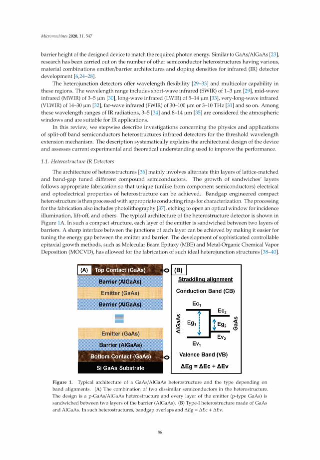
Micromachines 2020, 11, 547
barrier height of the designed device to match the required photon energy. Similar to GaAs/AlGaAs [23],research has been carried out on the number of other semiconductor heterostructures having various,material combinations emitter/barrier architectures and doping densities for infrared (IR) detectordevelopment [6,24–28].
The heterojunction detectors offer wavelength flexibility [29–33] and multicolor capability inthese regions. The wavelength range includes short-wave infrared (SWIR) of 1–3 μm [29], mid-waveinfrared (MWIR) of 3–5 μm [30], long-wave infrared (LWIR) of 5–14 μm [33], very-long-wave infrared(VLWIR) of 14–30 μm [32], far-wave infrared (FWIR) of 30–100 μm or 3–10 THz [31] and so on. Amongthese wavelength ranges of IR radiations, 3–5 [34] and 8–14 μm [35] are considered the atmosphericwindows and are suitable for IR applications.
In this review, we stepwise describe investigations concerning the physics and applicationsof split-off band semiconductors heterostructures infrared detectors for the threshold wavelengthextension mechanism. The description systematically explains the architectural design of the deviceand assesses current experimental and theoretical understanding used to improve the performance.
1.1. Heterostructure IR Detectors
The architecture of heterostructures [36] mainly involves alternate thin layers of lattice-matchedand band-gap tuned different compound semiconductors. The growth of sandwiches’ layersfollows appropriate fabrication so that unique (unlike from component semiconductors) electricaland optoelectrical properties of heterostructure can be achieved. Bandgap engineered compactheterostructure is then processed with appropriate conducting rings for characterization. The processingfor the fabrication also includes photolithography [37], etching to open an optical window for incidenceillumination, lift-off, and others. The typical architecture of the heterostructure detector is shown inFigure 1A. In such a compact structure, each layer of the emitter is sandwiched between two layers ofbarriers. A sharp interface between the junctions of each layer can be achieved by making it easier fortuning the energy gap between the emitter and barrier. The development of sophisticated controllableepitaxial growth methods, such as Molecular Beam Epitaxy (MBE) and Metal-Organic Chemical VaporDeposition (MOCVD), has allowed for the fabrication of such ideal heterojunction structures [38–40].
Figure 1. Typical architecture of a GaAs/AlGaAs heterostructure and the type depending onband alignments. (A) The combination of two dissimilar semiconductors in the heterostructure.The design is a p-GaAs/AlGaAs heterostructure and every layer of the emitter (p-type GaAs) issandwiched between two layers of the barrier (AlGaAs). (B) Type-I heterostructure made of GaAsand AlGaAs. In such heterostructures, bandgap overlaps and ΔEg = ΔEc + ΔEv.
86
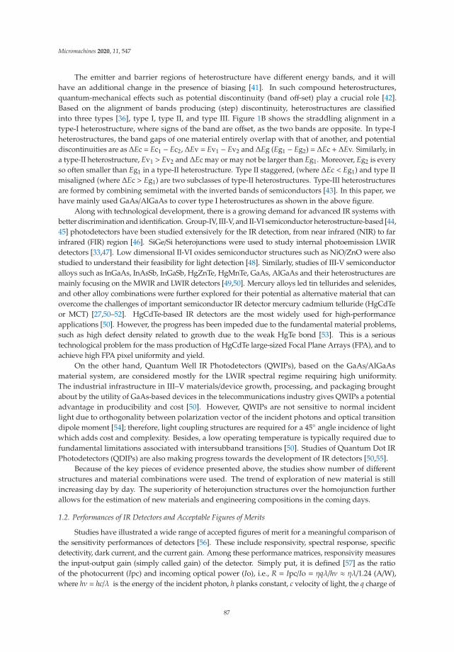
Micromachines 2020, 11, 547
The emitter and barrier regions of heterostructure have different energy bands, and it willhave an additional change in the presence of biasing [41]. In such compound heterostructures,quantum-mechanical effects such as potential discontinuity (band off-set) play a crucial role [42].Based on the alignment of bands producing (step) discontinuity, heterostructures are classifiedinto three types [36], type I, type II, and type III. Figure 1B shows the straddling alignment in atype-I heterostructure, where signs of the band are offset, as the two bands are opposite. In type-Iheterostructures, the band gaps of one material entirely overlap with that of another, and potentialdiscontinuities are as ΔEc = Ec1 − Ec2, ΔEv = Ev1 − Ev2 and ΔEg (Eg1 − Eg2) = ΔEc + ΔEv. Similarly, ina type-II heterostructure, Ev1 > Ev2 and ΔEc may or may not be larger than Eg1. Moreover, Eg2 is everyso often smaller than Eg1 in a type-II heterostructure. Type II staggered, (where ΔEc < Eg1) and type IImisaligned (where ΔEc > Eg1) are two subclasses of type-II heterostructures. Type-III heterostructuresare formed by combining semimetal with the inverted bands of semiconductors [43]. In this paper, wehave mainly used GaAs/AlGaAs to cover type I heterostructures as shown in the above figure.
Along with technological development, there is a growing demand for advanced IR systems withbetter discrimination and identification. Group-IV, III-V, and II-VI semiconductor heterostructure-based [44,45] photodetectors have been studied extensively for the IR detection, from near infrared (NIR) to farinfrared (FIR) region [46]. SiGe/Si heterojunctions were used to study internal photoemission LWIRdetectors [33,47]. Low dimensional II-VI oxides semiconductor structures such as NiO/ZnO were alsostudied to understand their feasibility for light detection [48]. Similarly, studies of III-V semiconductoralloys such as InGaAs, InAsSb, InGaSb, HgZnTe, HgMnTe, GaAs, AlGaAs and their heterostructures aremainly focusing on the MWIR and LWIR detectors [49,50]. Mercury alloys led tin tellurides and selenides,and other alloy combinations were further explored for their potential as alternative material that canovercome the challenges of important semiconductor IR detector mercury cadmium telluride (HgCdTeor MCT) [27,50–52]. HgCdTe-based IR detectors are the most widely used for high-performanceapplications [50]. However, the progress has been impeded due to the fundamental material problems,such as high defect density related to growth due to the weak HgTe bond [53]. This is a serioustechnological problem for the mass production of HgCdTe large-sized Focal Plane Arrays (FPA), and toachieve high FPA pixel uniformity and yield.
On the other hand, Quantum Well IR Photodetectors (QWIPs), based on the GaAs/AlGaAsmaterial system, are considered mostly for the LWIR spectral regime requiring high uniformity.The industrial infrastructure in III–V materials/device growth, processing, and packaging broughtabout by the utility of GaAs-based devices in the telecommunications industry gives QWIPs a potentialadvantage in producibility and cost [50]. However, QWIPs are not sensitive to normal incidentlight due to orthogonality between polarization vector of the incident photons and optical transitiondipole moment [54]; therefore, light coupling structures are required for a 45◦ angle incidence of lightwhich adds cost and complexity. Besides, a low operating temperature is typically required due tofundamental limitations associated with intersubband transitions [50]. Studies of Quantum Dot IRPhotodetectors (QDIPs) are also making progress towards the development of IR detectors [50,55].
Because of the key pieces of evidence presented above, the studies show number of differentstructures and material combinations were used. The trend of exploration of new material is stillincreasing day by day. The superiority of heterojunction structures over the homojunction furtherallows for the estimation of new materials and engineering compositions in the coming days.
1.2. Performances of IR Detectors and Acceptable Figures of Merits
Studies have illustrated a wide range of accepted figures of merit for a meaningful comparison ofthe sensitivity performances of detectors [56]. These include responsivity, spectral response, specificdetectivity, dark current, and the current gain. Among these performance matrices, responsivity measuresthe input-output gain (simply called gain) of the detector. Simply put, it is defined [57] as the ratioof the photocurrent (Ipc) and incoming optical power (Io), i.e., R = Ipc/Io = ηqλ/hν ≈ ηλ/1.24 (A/W),where hν = hc/λ is the energy of the incident photon, h planks constant, c velocity of light, the q charge of
87
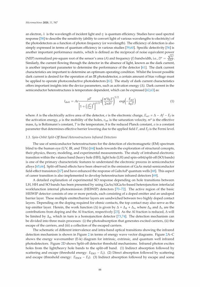
Micromachines 2020, 11, 547
an electron, λ is the wavelength of incident light and η is quantum efficiency. Studies have used spectralresponse [58] to describe the sensitivity (ability to convert light of various wavelengths to electricity) ofthe photodetectors as a function of photon frequency (or wavelength). The efficiency of detection is alsosimply expressed in terms of quantum efficiency in various studies [59,60]. Specific detectivity [56] isanother important performance matrix, which is defined as the reciprocal of noise equivalent power
(NEP) normalized pre-square root of the sensor’s area (A) and frequency (f ) bandwidth, i.e., D∗ =√
A fNEP .
Similarly, the current flowing through the detector in the absence of light, known as the dark current,is another important parameter to determine the performance of the detector [61]. The dark currentcharacteristics are important to determine an optimum operating condition. Whilst the lowest possibledark current is desired for the operation of an IR photodetector, a certain amount of bias voltage mustbe applied to operate photoconductive photodetectors [61]. The study of dark current characteristicsoffers important insights into the device parameters, such as activation energy (Δ). Dark current in thesemiconductor heterostructures is temperature dependent, which can be expressed [62,63] as:
Idark = AeμF[
1 +( μF
vsat
)2]1/22(
m∗kBT2π�2
)3/2
exp(−Eact
kBT
)(1)
where A is the electrically active area of the detector, e is the electronic charge, Eact = Δ − Af − Ef isthe activation energy, μ is the mobility of the holes, vsat is the saturation velocity, m* is the effectivemass, kB is Boltzmann’s constant, T is the temperature, h is the reduced Planck constant, α is a constantparameter that determines effective barrier lowering due to the applied field F, and Ef is the Fermi level.
1.3. Spin-Orbit Split-Off Band Heterostructures Infrared Detectors
The use of semiconductor heterostructures for the detection of electromagnetic (EM) spectrumblind to the human eye (UV, IR, and THz) [64] leads towards the exploration of structural concepts,their physics, theory, modeling, and experimental measurements. The study of intraband electronictransition within the valance band (heavy hole (HH), light hole (LH) and spin-orbit/split-off (SO) bands)is one of the primary characteristic features to understand the electronic process in semiconductoralloys [65,66]. Split-off band effects have been observed in the emission of GaAs metal-semiconductorfield-effect transistors [67] and have enhanced the response of GaInAsP quantum wells [68]. This aspectof career transition is also implemented to develop heterostructure infrared detectors [69].
A detailed explanation of experimental SO response depending on hole transitions betweenLH, HH and SO bands has been presented by using GaAs/AlGaAs-based heterojunction interfacialworkfunction internal photoemission (HEIWIP) detectors [70–72]. The active region of the basicHEIWIP detector consists of one or more periods, each consisting of a doped emitter and an undopedbarrier layer. These multiple emitter/barrier layers are sandwiched between two highly doped contactlayers. Depending on the doping required for ohmic contacts, the top contact may also serve as thetop emitter layer. Herein, the work function (Δ) is given by Δ = Δd + Δx, where Δd and Δx are thecontributions from doping and the Al fraction, respectively [23]. As the Al fraction is reduced, Δ willbe limited by Δd, which in turn is a homojunction detector [73,74]. The detection mechanism canbe divided into three main processes: (i) the photoabsorption that generates excited carriers, (ii) theescape of the carriers, and (iii) a collection of the escaped carriers.
The schematic of different intervalence and intra-band optical transitions showing the infrareddetection mechanism is shown in Figure 2 in terms of energy wave vector diagrams. Figure 2A–Cshows the energy wavenumber (E-k) diagram for intrinsic, extrinsic, and quantum well infraredphotodetectors. Figure 2D shows Split-off detector threshold mechanisms. Infrared photon excitesholes from the light/heavy hole bands to the split-off band. (1) Indirect absorption followed byscattering and escape (threshold energy: EESO − Ef). (2) Direct absorption followed by scatteringand escape (threshold energy: EESOf − Ef). (3) Indirect absorption followed by escape and some
88
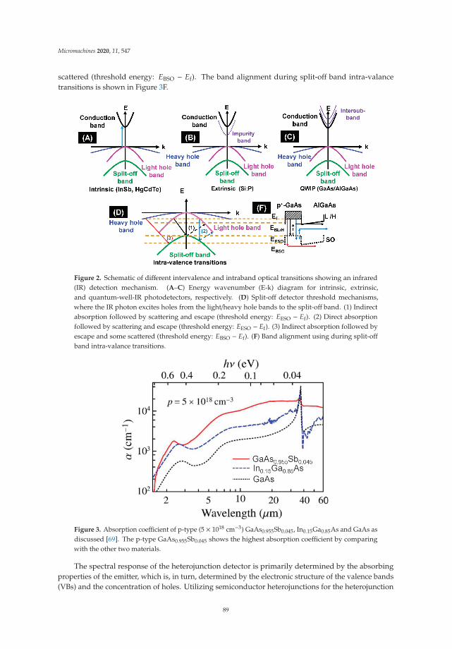
Micromachines 2020, 11, 547
scattered (threshold energy: EBSO − Ef). The band alignment during split-off band intra-valancetransitions is shown in Figure 3F.
Figure 2. Schematic of different intervalence and intraband optical transitions showing an infrared(IR) detection mechanism. (A–C) Energy wavenumber (E-k) diagram for intrinsic, extrinsic,and quantum-well-IR photodetectors, respectively. (D) Split-off detector threshold mechanisms,where the IR photon excites holes from the light/heavy hole bands to the split-off band. (1) Indirectabsorption followed by scattering and escape (threshold energy: EESO − Ef). (2) Direct absorptionfollowed by scattering and escape (threshold energy: EESO − Ef). (3) Indirect absorption followed byescape and some scattered (threshold energy: EBSO − Ef). (F) Band alignment using during split-offband intra-valance transitions.
Figure 3. Absorption coefficient of p-type (5 × 1018 cm−3) GaAs0.955Sb0.045, In0.15Ga0.85As and GaAs asdiscussed [69]. The p-type GaAs0.955Sb0.045 shows the highest absorption coefficient by comparingwith the other two materials.
The spectral response of the heterojunction detector is primarily determined by the absorbingproperties of the emitter, which is, in turn, determined by the electronic structure of the valence bands(VBs) and the concentration of holes. Utilizing semiconductor heterojunctions for the heterojunction
89
Micromachines 2020, 11, 547
detectors is subject to limitations, such as low absorption coefficient in the 3–5μm range for p-type GaAs.The p-type semiconductor absorbs extra photons owing to optical transitions among three VBs, i.e., theLH, HH, and SO bands, contributing to an absorption band spanning primarily from 1 to 10 μm forp-type GaAs, as shown in Figure 3. The p-type semiconductors including InGaAs, GaAsSb, and GaAsindicate that the shifting of the absorption peak (between 1 and 5 μm) can be associated with the SO–HHtransition. The intra-band free-carrier absorption is typically proportional to λp, which becomesdominant in the very-long-wavelength range, where λ is the wavelength, and p is an exponent. p canbe predicted by the Drude theory, and usually equals 1.2, 2.5, and 3.5 correspondings to scatterings byacoustic phonons, polar optical phonons, and ionized impurities, respectively. By comparing withp-type GaAs, p-type GaAsSb shows a higher absorption, which benefits a higher absorption efficiencyand hence the detector performance.
Jayaweera et al. studied an uncooled infrared detector for 3–5 μm and beyond [75] by usingthe concept of a split-off band infrared detection mechanism [70,71]. In their study, they haveexperimentally demonstrated uncooled infrared detection using intra-valence bands using a set ofthree p-GaAs/AlGaAs heterostructure. The focus of their study is to demonstrate an uncooled infrareddetection using intra-valence bands. The uncooled detection of infrared radiation is important ina wide range of applications in the civilian, industrial, medical, astronomy, and military sectors.The calculated D* value in this study is 6.8 × 10⁵ Jones at a temperature of 300 K and an SO band offsetof 0.31 eV, while, for those with an SO band offset of 0.155 and 0.207 eV, D* values are 2.1 × 10⁶
and 1.8 × 10⁶ at temperatures of 140 and 190 K, respectively. It is noted that the studies on the highoperating temperature that split off the transition in such a heterostructure [70–72] further support theinfrared detection mechanism. These studies have introduced intra-valence band transitions, such asLH to heavy-hole HH transitions or HH transitions to SO band in detectors to overcome the selectionrule limitations. A band diagram (E-k) of the emitter region of an S-O band detector illustrating thedetection mechanism is based on the carrier transitions in the three valence bands is also demonstrated.
In the study by Lao and et al. [76], the development of structure with multi-spectral detectionprobability is presented. The hole transition from the HH to the LH band of p-GaAs/AlGaAs detectorsshow a spectral response up to 16.5 m, operating up to a temperature of 330 K where the LH-HHresponse is superimposed on the free-carrier response. Similarly, in another study by Matsik, and etal. [77] device modeling study of S-O band IR detector was carried out to find optimized conditions forits performance improvement. The study suggested two important device architecture modificationsin order to improve device performance. One of the suggestions was to include an offset (δE) betweenthe energy barriers so that the low energy barrier towards the collector side would enhance thecollection. The other suggestion was to include a graded barrier on the injector side so that the carriertrapping would be reduced and the injection of the carriers to the absorber/emitter would be improved.
Altogether, the peak response due to intra-valance band transitions [70,71,78] is believed tooriginate from a build-up of a quasi-equilibrium Fermi level, at a fixed level, irrespective of thevariation of the device parameter. Thus, the SO band was found to be the most probable energy levelto build-up a quasi-equilibrium Fermi level as a consequence of the hot-phonon bottleneck effect.The study of the dark current characteristics of these IR photodetectors confirmed no compromise inthe dark current due to the presence of the extended-wavelength mechanism of the photoresponse.Furthermore, the quasi-equilibrium will be built-up not only in the emitter but also in the bottom and topcontact layers as long as there is photoexcitation to the SO band. The net flow of the photo-excitedcarriers will determine the spectral photoresponse [62,79].
In summary, HEIWIP detectors [80], based on intra-valence band transitions LH to HH transitions orHH transitions to SO band were introduced to overcome the selection rule limitations. The SO band infrareddetector is a newly developed, emerging device based on the p-doped GaAs/AlGaAs system [71], whichutilizes hole transition in the HH/LH band to the SO band as the detection mechanism [71]. The SOband detectors have shown promising results to be developed as an uncooled IR detector [75].
90
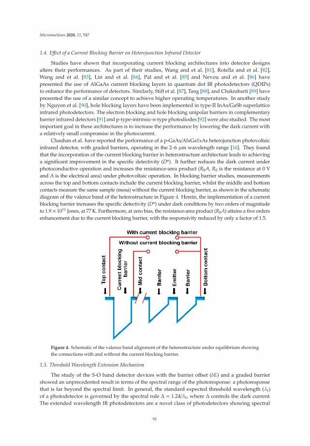
Micromachines 2020, 11, 547
1.4. Effect of a Current Blocking Barrier on Heterojunction Infrared Detector
Studies have shown that incorporating current blocking architectures into detector designsalters their performances. As part of their studies, Wang and et al. [81], Rotella and et al. [82],Wang and et al. [83], Lin and et al. [84], Pal and et al. [85] and Nevou and et al. [86] havepresented the use of AlGaAs current blocking layers in quantum dot IR photodetectors (QDIPs)to enhance the performance of detectors. Similarly, Stiff et al. [87], Tang [88], and Chakrabarti [89] havepresented the use of a similar concept to achieve higher operating temperatures. In another studyby Nguyen et al. [90], hole blocking layers have been implemented in type-II InAs/GaSb superlatticeinfrared photodetectors. The electron blocking and hole blocking unipolar barriers in complementarybarrier infrared detectors [91] and p-type-intrinsic-n-type photodiodes [92] were also studied. The mostimportant goal in these architectures is to increase the performance by lowering the dark current witha relatively small compromise in the photocurrent.
Chauhan et al. have reported the performance of a p-GaAs/AlxGa1xAs heterojunction photovoltaicinfrared detector, with graded barriers, operating in the 2–6 μm wavelength range [16]. They foundthat the incorporation of the current blocking barrier in heterostructure architecture leads to achievinga significant improvement in the specific detectivity (D*). It further reduces the dark current underphotoconductive operation and increases the resistance-area product (R0A, R0 is the resistance at 0 Vand A is the electrical area) under photovoltaic operation. In blocking barrier studies, measurementsacross the top and bottom contacts include the current blocking barrier, whilst the middle and bottomcontacts measure the same sample (mesa) without the current blocking barrier, as shown in the schematicdiagram of the valence band of the heterostructure in Figure 4. Herein, the implementation of a currentblocking barrier increases the specific detectivity (D*) under dark conditions by two orders of magnitudeto 1.9 × 10¹¹ Jones, at 77 K. Furthermore, at zero bias, the resistance-area product (R0A) attains a five ordersenhancement due to the current blocking barrier, with the responsivity reduced by only a factor of 1.5.
Figure 4. Schematic of the valence band alignment of the heterostructure under equilibrium showingthe connections with and without the current blocking barrier.
1.5. Threshold Wavelength Extension Mechanism
The study of the S-O band detector devices with the barrier offset (δE) and a graded barriershowed an unprecedented result in terms of the spectral range of the photoresponse: a photoresponsethat is far beyond the spectral limit. In general, the standard expected threshold wavelength (λt)of a photodetector is governed by the spectral rule Δ = 1.24/λt, where Δ controls the dark current.The extended wavelength IR photodetectors are a novel class of photodetectors showing spectral
91
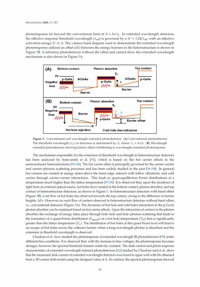
Micromachines 2020, 11, 547
photoresponse far beyond the conventional limit of Δ = hc/λt. In extended wavelength detectors,the effective response threshold wavelength (λeff) is governed by a Δ′ = 1.24/λeff, with an effectiveactivation energy Δ′ Δ. The valance band diagram used to demonstrate the extended wavelengthphotoresponse utilized an offset (δE) between the energy barriers in the heterostructure is shown inFigure 5B. A reference photodetector without the offset and cannot show the extended wavelengthmechanism is also shown in Figure 5A.
Figure 5. Conventional and wavelength extended photodetector. (A) Conventional photodetector.The threshold wavelength (λc) of detection is determined by Δ, where λc = hc/Δ. (B) Wavelengthextended photodetector showing barrier offset contributing to wavelength-extended photoresponse.
The mechanism responsible for the extension of threshold wavelength in heterostructure detectorshas been analyzed by Somvanshi et al. [93], which is based on the hot carrier effects in thesemiconductor heterostructures [94–96]. The hot carrier effect is principally governed by the carrier–carrierand carrier–phonon scattering processes and has been widely studied in the past [96–98]. In general,hot carriers are created in energy states above the band edge, interact with lattice vibrations, and coldcarries through carrier–carrier interactions. This leads to quasi-equilibrium Fermi distributions at atemperature much higher than the lattice temperature [97,98]. It is observed that, upon the incidence oflight from an external optical source, hot holes have created in the bottom contact, photon absorber, and topcontact of heterostructure detectors, as shown in Figure 5. In heterostructure detectors with band offset(Figure 5B), a net flow of hot holes has observed towards the top contact, owing to the difference in barrierheights, ΔEv. However, no such flow of carriers observed in heterostructure detectors without band offset,i.e., conventional detectors (Figure 5A). The dynamics of hot hols and cold holes interaction in the p-GaAsphoton absorber can be explained based on hot carrier effects. Upon the interaction of carriers in the photonabsorber, the exchange of energy takes place through hole–hole and hole–phonon scattering that leads tothe formation of a quasi-Fermi distribution (EquasiF) at a hot hole temperature (TH) that is significantlygreater than the lattice temperature (TL). The distribution of hot holes at this quasi-Fermi level will lead toan escape of hot holes across the collector barrier when a long-wavelength photon is absorbed and theextension in threshold wavelength is observed.
Chauhan et al. have studied the photoresponse of extended wavelength IR photodetectors [99] underdifferent bias conditions. It is observed that, with the increase in bias voltages, the photoresponse becomesstronger; however, the spectral threshold remains relatively constant. The dark current and photo-responsecharacteristics of extended wavelength infrared photodetectors [62] studied by Chauhan and et al. showthat the measured dark current of extended wavelength detectors was found to agree well with fits obtainedfrom a 3D carrier drift model using the designed value of Δ. In contrast, the spectral photoresponse showed
92
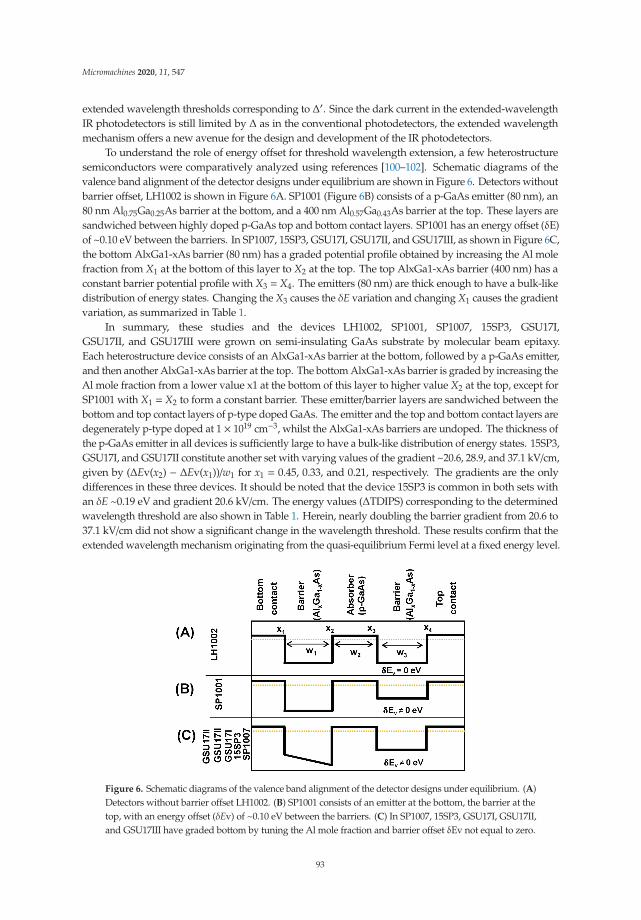
Micromachines 2020, 11, 547
extended wavelength thresholds corresponding to Δ′. Since the dark current in the extended-wavelengthIR photodetectors is still limited by Δ as in the conventional photodetectors, the extended wavelengthmechanism offers a new avenue for the design and development of the IR photodetectors.
To understand the role of energy offset for threshold wavelength extension, a few heterostructuresemiconductors were comparatively analyzed using references [100–102]. Schematic diagrams of thevalence band alignment of the detector designs under equilibrium are shown in Figure 6. Detectors withoutbarrier offset, LH1002 is shown in Figure 6A. SP1001 (Figure 6B) consists of a p-GaAs emitter (80 nm), an80 nm Al0.75Ga0.25As barrier at the bottom, and a 400 nm Al0.57Ga0.43As barrier at the top. These layers aresandwiched between highly doped p-GaAs top and bottom contact layers. SP1001 has an energy offset (δE)of ~0.10 eV between the barriers. In SP1007, 15SP3, GSU17I, GSU17II, and GSU17III, as shown in Figure 6C,the bottom AlxGa1-xAs barrier (80 nm) has a graded potential profile obtained by increasing the Al molefraction from X1 at the bottom of this layer to X2 at the top. The top AlxGa1-xAs barrier (400 nm) has aconstant barrier potential profile with X3 = X4. The emitters (80 nm) are thick enough to have a bulk-likedistribution of energy states. Changing the X3 causes the δE variation and changing X1 causes the gradientvariation, as summarized in Table 1.
In summary, these studies and the devices LH1002, SP1001, SP1007, 15SP3, GSU17I,GSU17II, and GSU17III were grown on semi-insulating GaAs substrate by molecular beam epitaxy.Each heterostructure device consists of an AlxGa1-xAs barrier at the bottom, followed by a p-GaAs emitter,and then another AlxGa1-xAs barrier at the top. The bottom AlxGa1-xAs barrier is graded by increasing theAl mole fraction from a lower value x1 at the bottom of this layer to higher value X2 at the top, except forSP1001 with X1 = X2 to form a constant barrier. These emitter/barrier layers are sandwiched between thebottom and top contact layers of p-type doped GaAs. The emitter and the top and bottom contact layers aredegenerately p-type doped at 1 × 1019 cm−3, whilst the AlxGa1-xAs barriers are undoped. The thickness ofthe p-GaAs emitter in all devices is sufficiently large to have a bulk-like distribution of energy states. 15SP3,GSU17I, and GSU17II constitute another set with varying values of the gradient ~20.6, 28.9, and 37.1 kV/cm,given by (ΔEv(x2) − ΔEv(x1))/w1 for x1 = 0.45, 0.33, and 0.21, respectively. The gradients are the onlydifferences in these three devices. It should be noted that the device 15SP3 is common in both sets withan δE ~0.19 eV and gradient 20.6 kV/cm. The energy values (ΔTDIPS) corresponding to the determinedwavelength threshold are also shown in Table 1. Herein, nearly doubling the barrier gradient from 20.6 to37.1 kV/cm did not show a significant change in the wavelength threshold. These results confirm that theextended wavelength mechanism originating from the quasi-equilibrium Fermi level at a fixed energy level.
Figure 6. Schematic diagrams of the valence band alignment of the detector designs under equilibrium. (A)Detectors without barrier offset LH1002. (B) SP1001 consists of an emitter at the bottom, the barrier at thetop, with an energy offset (δEv) of ~0.10 eV between the barriers. (C) In SP1007, 15SP3, GSU17I, GSU17II,and GSU17III have graded bottom by tuning the Al mole fraction and barrier offset δEv not equal to zero.
93
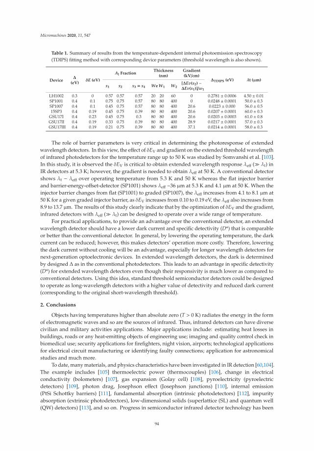
Micromachines 2020, 11, 547
Table 1. Summary of results from the temperature-dependent internal photoemission spectroscopy(TDIPS) fitting method with corresponding device parameters (threshold wavelength is also shown).
DeviceΔ
(eV)δE (eV)
Al FractionThickness
(nm)Gradient(kV/cm)
ΔTDIPS (eV) λt (μm)
x1 x2 x3 = x4 We W1 W2[ΔEv(x2) −ΔEv(x1)]/w1
LH1002 0.3 0 0.57 0.57 0.57 20 20 60 0 0.2781 ± 0.0006 4.50 ± 0.01SP1001 0.4 0.1 0.75 0.75 0.57 80 80 400 0 0.0248 ± 0.0001 50.0 ± 0.3SP1007 0.4 0.1 0.45 0.75 0.57 80 80 400 20.6 0.0223 ± 0.000 56.0 ± 0.515SP3 0.4 0.19 0.45 0.75 0.39 80 80 400 20.6 0.0207 ± 0.0001 60.0 ± 0.3
GSU17I 0.4 0.23 0.45 0.75 0.3 80 80 400 20.6 0.0203 ± 0.0003 61.0 ± 0.8GSU17II 0.4 0.19 0.33 0.75 0.39 80 80 400 28.9 0.0217 ± 0.0001 57.0 ± 0.3GSU17III 0.4 0.19 0.21 0.75 0.39 80 80 400 37.1 0.0214 ± 0.0001 58.0 ± 0.3
The role of barrier parameters is very critical in determining the photoresponse of extendedwavelength detectors. In this view, the effect of δEV and gradient on the extended threshold wavelengthof infrared photodetectors for the temperature range up to 50 K was studied by Somvanshi et al. [103].In this study, it is observed the δEV is critical to obtain extended wavelength response λeff (� λt) inIR detectors at 5.3 K; however, the gradient is needed to obtain λeff at 50 K. A conventional detectorshows λt − λeff over operating temperature from 5.3 K and 50 K whereas the flat injector barrierand barrier-energy-offset-detector (SP1001) shows λeff ~36 μm at 5.3 K and 4.1 μm at 50 K. When theinjector barrier changes from flat (SP1001) to graded (SP1007), the λeff increases from 4.1 to 8.1 μm at50 K for a given graded injector barrier, as δEV increases from 0.10 to 0.19 eV, the λeff also increases from8.9 to 13.7 μm. The results of this study clearly indicate that by the optimization of δEV and the gradient,infrared detectors with λeff (� λt) can be designed to operate over a wide range of temperature.
For practical applications, to provide an advantage over the conventional detector, an extendedwavelength detector should have a lower dark current and specific detectivity (D*) that is comparableor better than the conventional detector. In general, by lowering the operating temperature, the darkcurrent can be reduced; however, this makes detectors’ operation more costly. Therefore, loweringthe dark current without cooling will be an advantage, especially for longer wavelength detectors fornext-generation optoelectronic devices. In extended wavelength detectors, the dark is determinedby designed Δ as in the conventional photodetectors. This leads to an advantage in specific detectivity(D*) for extended wavelength detectors even though their responsivity is much lower as compared toconventional detectors. Using this idea, standard threshold semiconductor detectors could be designedto operate as long-wavelength detectors with a higher value of detectivity and reduced dark current(corresponding to the original short-wavelength threshold).
2. Conclusions
Objects having temperatures higher than absolute zero (T > 0 K) radiates the energy in the formof electromagnetic waves and so are the sources of infrared. Thus, infrared detectors can have diversecivilian and military activities applications. Major applications include: estimating heat losses inbuildings, roads or any heat-emitting objects of engineering use; imaging and quality control check inbiomedical use; security applications for firefighters, night vision, airports; technological applicationsfor electrical circuit manufacturing or identifying faulty connections; application for astronomicalstudies and much more.
To date, many materials, and physics characteristics have been investigated in IR detection [60,104].The example includes [105] thermoelectric power (thermocouples) [106], change in electricalconductivity (bolometers) [107], gas expansion (Golay cell) [108], pyroelectricity (pyroelectricdetectors) [109], photon drag, Josephson effect (Josephson junctions) [110], internal emission(PtSi Schottky barriers) [111], fundamental absorption (intrinsic photodetectors) [112], impurityabsorption (extrinsic photodetectors), low-dimensional solids (superlattice (SL) and quantum well(QW) detectors) [113], and so on. Progress in semiconductor infrared detector technology has been
94
Micromachines 2020, 11, 547
made in IR detector technology to improve their performance. Furthermore, studies are going on for theimprovement of detector performances. In reference to this, potential applications of a heterostructureIR detector working within a wide range of temperatures, including a room-temperature environment,can be anticipated. Of course, innovation in the heterostructure architecture of thoroughly documentedsemiconductor compounds will create another degree of freedom in recent technology.
This study documented the present studies on the S-O band energy, and H-H/L-H transitions giverise to the photoresponse in heterostructure infrared detectors with a peak in the 3–5 μm regime, withthe most important band being an atmospheric window. The incorporation of current blocking barriersto lower the dark current density and to increase the performance of heterostructure semiconductordetectors is also discussed. The importance of the wavelength threshold extension mechanism isalso clearly illustrated, with its application for future IR photodetector design and development.Finally, a considerable achievement in the practical application of a new kind (unlike the conventional)of IR photodetectors, with the wavelength threshold determined in the near future, can be anticipated.
Photovoltaic infrared sensor arrays for the 3–5 μm and 8–12 μm atmospheric windows canbe fabricated using similar techniques. GaAs/AlGaAs heterostructures can overcome the serioustechnological problem for the mass production of HgCdTe large-sized Focal Plane Arrays (FPA) [114],and to achieve high FPA pixel uniformity and yield. Large line or area arrays of such photovoltaicinfrared detectors can be desired for thermal imaging and spectroscopic applications.
Author Contributions: Conceptualization, A.G.U.P.; writing—original draft preparation, H.G.; supervision,A.G.U.P.; writing—review and editing, P.V.V.J., D.S., Y.L., and A.G.U.P. All authors have read and agreed to thepublished version of the manuscript.
Funding: U.S. Army Research Office (ARO) (W911 NF-15-1-0018).
Acknowledgments: H. Ghimire acknowledges support from Molecular Basis of Disease (MBD) at GSU.
Conflicts of Interest: The authors declare no conflict of interest.
References
1. Weisbuch, C.; Vinter, B. Quantum Semiconductor Structures: Fundamentals and Applications; Elsevier: Amsterdam,The Netherlands, 2014.
2. Bhimanapati, G.R.; Lin, Z.; Meunier, V.; Jung, Y.; Cha, J.; Das, S.; Xiao, D.; Son, Y.; Strano, M.S.; Cooper, V.R.;et al. Recent Advances in Two-Dimensional Materials beyond Graphene. ACS Nano 2015, 9, 11509–11539.[CrossRef]
3. Petroff, P.; DenBaars, S. MBE and MOCVD growth and properties of self-assembling quantum dot arrays inIII-V semiconductor structures. Superlattices Microstruct. 1994, 15, 15. [CrossRef]
4. Neamen, D.A. Semiconductor Physics and Devices: Basic Principles; McGraw-Hill: New York, NY, USA, 2012.5. Nguyen, B.-M.; Hoffman, D.; Delaunay, P.-Y.; Razeghi, M. Dark current suppression in type II InAs/GaSb
superlattice long wavelength infrared photodiodes with M-structure barrier. Appl. Phys. Lett. 2007, 91, 163511.[CrossRef]
6. Krishna, S. Quantum dots-in-a-well infrared photodetectors. J. Phys. D Appl. Phys. 2005, 38, 2142. [CrossRef]7. Karunasiri, R.; Park, J.; Wang, K. Si1−x Ge x/Si multiple quantum well infrared detector. Appl. Phys. Lett.
1991, 59, 2588–2590. [CrossRef]8. Gunapala, S.D.; Bandara, S.V.; Singh, A.; Liu, J.K.; Rafol, B.; Luong, E.; Mumolo, J.M.; Tran, N.Q.; Ting, D.Z.-Y.;
Vincent, J.D.; et al. 640/spl times/486 long-wavelength two-color GaAs/AlGaAs quantum well infraredphotodetector (QWIP) focal plane array camera. IEEE Trans. Electron Devices 2000, 47, 963–971. [CrossRef]
9. Chang, K.H.; Bhattacharya, P.K.; Gibala, R. Characteristics of dislocations at strained heteroepitaxialInGaAs/GaAs interfaces. J. Appl. Phys. 1989, 66, 2993–2998. [CrossRef]
10. Aziziyan, M.R.; Hassen, W.M. Electrically biased GaAs/AlGaAs heterostructures for enhanced detection ofbacteria. Synth. Photonics Nanoscale Mater. Xiii 2016, 9737, 97370. [CrossRef]
11. Dingle, R.; Wiegmann, W.; Henry, C.H. Quantum states of confined carriers in very thin Al x Ga 1− xAs-GaAs-Al x Ga 1− x As heterostructures. Phys. Rev. Lett. 1974, 33, 827. [CrossRef]
95
Micromachines 2020, 11, 547
12. Adachi, S. GaAs, AlAs, and Al x Ga1− x As: Material parameters for use in research and device applications.J. Appl. Phys. 1985, 58, R1–R29. [CrossRef]
13. Yablonovitch, E.; Kapon, E.; Gmitter, T.; Yun, C.; Bhat, R. Double heterostructure GaAs/AlGaAs thin filmdiode lasers on glass substrates. IEEE Photon Technol. Lett. 1989, 1, 41–42. [CrossRef]
14. Tomioka, K.; Motohisa, J.; Hara, S.; Hiruma, K.; Fukui, T. GaAs/AlGaAs Core Multishell Nanowire-BasedLight-Emitting Diodes on Si. Nano Lett. 2010, 10, 1639–1644. [CrossRef]
15. Lade, S.J.; Zahedi, A. A revised ideal model for AlGaAs/GaAs quantum well solar cells. Microelectron. J.2004, 35, 401–410. [CrossRef]
16. Chauhan, D.; Perera, A.; Li, L.; Chen, L.; Linfield, E. Effect of a current blocking barrier on a 2–6 μ mp-GaAs/AlGaAs heterojunction infrared detector. Appl. Phys. Lett. 2016, 108, 201105. [CrossRef]
17. Gunapala, S.D.; Bundara, S.; Liu, J.K.; Hong, W.; Sundaram, M.; Maker, P.D.; Muller, R.E.; Shott, C.A.;Carralejo, R. Long-wavelength 640/spl times/486 GaAs-AlGaAs quantum well infrared photodetectorsnap-shot camera. IEEE Trans. Electron. Devices 1998, 45, 1890–1895. [CrossRef]
18. Gunapala, S.D.; Bandara, S.V.; Liu, J.K.; Luong, E.; Stetson, N.; Shott, C.A.; Bock, J.J.; Rafol, S.B.; Mumolo, J.M.;McKelvey, M.J. Long-wavelength 256/spl times/256 GaAs/AlGaAs quantum well infrared photodetector(QWIP) palm-size camera. IEEE Trans. Electron. Devices 2000, 47, 326–332. [CrossRef]
19. Weerasekara, A.; Rinzan, M.; Matsik, S.; Perera, A.G.; Buchanan, M.; Liu, H.C.; Von Winckel, G.; Stintz, A.;Krishna, S. n-Type GaAs/AlGaAs heterostructure detector with a 32 THz threshold frequency. Opt. Lett.2007, 32, 1335–1337. [CrossRef]
20. Dai, X.; Zhang, S.; Wang, Z.; Adamo, G.; Liu, H.; Huang, Y.; Couteau, C.; Soci, C. GaAs/AlGaAs NanowirePhotodetector. Nano Lett. 2014, 14, 2688–2693. [CrossRef]
21. Casey, H.C.; Panish, M.B. Heterostructure Lasers: Materials and Operating Characteristics; Academic Pr:Cambridge, MA, USA, 1978.
22. Chang, K.H.; Lee, C.P.; Wu, J.S.; Liu, D.G.; Liou, D.C.; Wang, M.H.; Chen, L.J.; Marais, M.A. Precisedetermination of aluminum content in AlGaAs. J. Appl. Phys. 1991, 70, 4877–4882. [CrossRef]
23. Esaev, D.; Rinzan, M.; Matsik, S.; Perera, A. Design and optimization of GaAs/AlGaAs heterojunction infrareddetectors. J. Appl. Phys. 2004, 96, 4588–4597. [CrossRef]
24. Rogalski, A.; Chrzanowski, K. 18 Infrared devices and techniques. In Nanophotonics and Plasmonics;Informa UK Ltd.: Colchester, UK, 2017; pp. 633–686.
25. Rogalski, A. Infrared and Terahertz Detectors; CRC Press: Boca Raton, FL, USA, 2019.26. Coon, D.D.; Karunasiri, R.P.G. New mode of IR detection using quantum wells. Appl. Phys. Lett. 1984,
45, 649. [CrossRef]27. Rogalski, A. Heterostructure infrared photovoltaic detectors. Infrared Phys. Technol. 2000, 41, 213–238.
[CrossRef]28. Ariyawansa, G.; Rinzan, M.B.M.; Alevli, M.; Strassburg, M.; Dietz, N.; Perera, A.G.U.; Matsik, S.G.; Asghar, A.;
Ferguson, I.T.; Luo, H.; et al. GaN/AlGaN ultraviolet/infrared dual-band detector. Appl. Phys. Lett. 2006,89, 091113. [CrossRef]
29. Perera, A.G.U. Heterojunction and superlattice detectors for infrared to ultraviolet. Prog. Quantum Electron.2016, 48, 1–56. [CrossRef]
30. Tong, J.; Tobing, L.Y.; Qiu, S.; Zhang, D.H.; Perera, A.U. Room temperature Plasmon-enhanced InAs0. 91Sb0.09-based heterojunction nip mid-wave infrared photodetector. Appl. Phys. Lett. 2018, 113, 011110. [CrossRef]
31. Kouvetakis, J.; Chizmeshya, A.V.G. New classes of Si-based photonic materials and device architectures viadesigner molecular routes. J. Mater. Chem. 2007, 17, 1649. [CrossRef]
32. Lin, Y.; Donetsky, D.; Wang, D.; Westerfeld, D.; Kipshidze, G.; Shterengas, L.; Sarney, W.L.; Svensson, S.P.;Belenky, G. Development of Bulk InAsSb Alloys and Barrier Heterostructures for Long-Wave InfraredDetectors. J. Electron. Mater. 2015, 44, 3360–3366. [CrossRef]
33. Tsaur, B.-Y.; Chen, C.; Marino, S. Long-wavelength Ge/sub x/Si/sub 1-x//Si heterojunction infrared detectorsand 400*400-element imager arrays. IEEE Electron. Device Lett. 1991, 12, 293–296. [CrossRef]
34. Harris, D.C. Durable 3–5 μm transmitting infrared window materials. Infrared Phys. Technol. 1998, 39, 185–201.[CrossRef]
35. Salisbury, J.W.; D’Aria, D.M. Emissivity of terrestrial materials in the 8–14 μm atmospheric window.Remote Sens. Environ. 1992, 42, 83–106. [CrossRef]
96
Micromachines 2020, 11, 547
36. Bastard, G.; Schulman, J. Wave Mechanics Applied to Semiconductor Heterostructures. Phys. Today 1992,45, 103. [CrossRef]
37. Moreau, W.M. Semiconductor Lithography: Principles, Practices, and Materials; Springer Science & Business Media:Berlin, Germany, 2012.
38. Pelzel, R. A comparison of MOVPE and MBE growth technologies for III-V epitaxial structures. In Proceedingsof the CS MANTECH Conference, New Orleans, LA, USA, 13–16 May 2013; pp. 105–108.
39. Tobin, S.; Vernon, S.; Bajgar, C.; Wojtczuk, S.; Melloch, M.; Keshavarzi, A.; Stellwag, T.; Venkatensan, S.;Lundström, M.; Emery, K. Assessment of MOCVD- and MBE-growth GaAs for high-efficiency solar cellapplications. IEEE Trans. Electron. Devices 1990, 37, 469–477. [CrossRef]
40. Horikoshi, Y.; Kawashima, M.; Yamaguchi, H. Migration-Enhanced Epitaxy of GaAs and AlGaAs. Jpn. J.Appl. Phys. 1988, 27, 169–179. [CrossRef]
41. Lundstrom, M.; Schuelke, R. Numerical analysis of heterostructure semiconductor devices. IEEE Trans.Electron. Devices 1983, 30, 1151–1159. [CrossRef]
42. Tersoff, J. Theory of semiconductor heterojunctions: The role of quantum dipoles. Phys. Rev. B 1984,30, 4874–4877. [CrossRef]
43. Capasso, F.; Cho, A.Y. Bandgap engineering of semiconductor heterostructures by molecular beam epitaxy:Physics and applications. Surf. Sci. 1994, 299, 878–891. [CrossRef]
44. Liu, Q.; Zhang, X.; Abdalla, L.B.; Zunger, A. Transforming Common III-V and II-VI SemiconductorCompounds into Topological Heterostructures: The Case of CdTe/InSb Superlattices. Adv. Funct. Mater.2016, 26, 3259–3267. [CrossRef]
45. Chang, K.H.; Gilbala, R.; Srolovitz, D.J.; Bhattacharya, P.K.; Mansfield, J.F. Crosshatched surface morphologyin strained III-V semiconductor films. J. Appl. Phys. 1990, 67, 4093–4098. [CrossRef]
46. Ting, D.Z.; Soibel, A.; Hill, C.; Nguyen, J.; Keo, S.; Rafol, S.B.; Yang, B.; Lee, M.C.; Mumolo, J.; Liu, J.; et al.Antimonide superlattice complementary barrier infrared detector (CBIRD). Infrared Phys. Technol. 2011,54, 267–272. [CrossRef]
47. Lin, T.; Maserjian, J. Novel Si1− x Ge x/Si heterojunction internal photoemission long-wavelength infrareddetectors. Appl. Phys. Lett. 1990, 57, 1422–1424. [CrossRef]
48. Yu, J.S.; Ko, Y.H.; Nagaraju, G. Low-dimensional II-VI oxide-based semiconductor nanostructurephotodetectors for light sensing. Quantum Sens. Nanophotonic Devices Xii 2015, 9370, 93702. [CrossRef]
49. Piotrowski, J.; Rogalski, A. New generation of infrared photodetectors. Sens. Actuators A Phys. 1998,67, 146–152. [CrossRef]
50. Rogalski, A. Recent progress in infrared detector technologies. Infrared Phys. Technol. 2011, 54, 136–154.[CrossRef]
51. Rogalski, A.; Adamiec, K.; Rutkowski, J. Narrow-Gap Semiconductor Photodiodes; SPIE Press: Bellingham, WA,USA, 2000; Volume 77.
52. Bratt, P.R. Potential barriers in HgCdTe heterojunctions. J. Vac. Sci. Technol. A 1985, 3, 238–245. [CrossRef]53. Rogalski, A. Infrared detectors: Status and trends. Prog. Quantum Electron. 2003, 27, 59–210. [CrossRef]54. Levine, B.F. Quantum-well infrared photodetectors. J. Appl. Phys. 1993, 74, 1. [CrossRef]55. Krishna, S.; Gunapala, S.; Bandara, S.; Hill, C.; Ting, D. Quantum Dot Based Infrared Focal Plane Arrays.
Proc. IEEE 2007, 95, 1838–1852. [CrossRef]56. Jones, R.C. Performance of Detectors for Visible and Infrared Radiation. In Advances in Electronics and Electron
Physics; Elsevier B.V.: Danvers, MA, USA, 1953; Volume 5, pp. 1–96.57. Paschotta, R. Avalanche photodiodes. Encycl. Laser Phys. Technol. 2008. Available online: https:
//www.rp-photonics.com/avalanche_photodiodes.html (accessed on 21 April 2020).58. Field, H. UV-VIS-IR spectral responsivity measurements system for solar cells. In Proceedings of
the National Center for photovoltaics (NCPV) 15th Program Review Meeting, Denver, CO, USA,9–11 September 1998; pp. 629–635. [CrossRef]
59. Andersson, J.Y.; Lundqvist, L. Near?unity quantum efficiency of AlGaAs/GaAs quantum well infrareddetectors using a waveguide with a doubly periodic grating coupler. Appl. Phys. Lett. 1991, 59, 857–859.[CrossRef]
60. Dereniak, E.L.; Boreman, G.D. Infrared Detectors and Systems; Wiley: New York, NY, USA, 1996; Volume 306.
97
Micromachines 2020, 11, 547
61. Cervera, C.; Baier, N.; Gravrand, O.; Mollard, L.; Lobre, C.; Destéfanis, G.; Zanatta, J.P.; Boulade, O.; Moreau, V.Low-dark current p-on-n MCT detector in long and very long-wavelength infrared. Infrared Technol. Appl. Xli2015, 9451, 945129. [CrossRef]
62. Chauhan, D.; Perera, A.G.U.; Li, L.; Chen, L.; Linfield, E.H. Dark current and photoresponse characteristicsof extended wavelength infrared photodetectors. J. Appl. Phys. 2017, 122, 024501. [CrossRef]
63. Weber, E.R.; Willardson, R.K.; Liu, H.; Capasso, F. Intersubband Transitions in Quantum Wells: Physics and DeviceApplications; Academic press: San Diego, CA, USA, 1999.
64. Bie, Y.-Q.; Liao, Z.-M.; Zhang, H.; Li, G.-R.; Ye, Y.; Zhou, Y.; Xu, J.; Qin, Z.-X.; Dai, L.; Yu, D. Self-Powered,Ultrafast, Visible-Blind UV Detection and Optical Logical Operation based on ZnO/GaN Nanoscale p-nJunctions. Adv. Mater. 2010, 23, 649–653. [CrossRef] [PubMed]
65. Vasko, F.T.; Kuznetsov, A.V. Electronic States and Optical Transitions in Semiconductor Heterostructures; SpringerScience and Business Media LLC: Berlin, Germany, 1999.
66. Souri, D.; Tahan, Z.E. A new method for the determination of optical band gap and the nature of opticaltransitions in semiconductors. Appl. Phys. A 2015, 119, 273–279. [CrossRef]
67. Zhuravlev, K.S.; A Kolosanov, V.; Milekhin, A.G.; Polovinkin, V.; Shamirzaev, T.S.; Rakov, Y.N.; Myakishev, Y.B.;Fryar, J.; McGlynn, E.; O Henry, M. Infrared light emission from GaAs MESFETs operating at avalanchebreakdown conditions. Semicond. Sci. Technol. 2004, 19, S94–S95. [CrossRef]
68. Hoff, J.; Razeghi, M.; Brown, G.J. Effect of the spin split-off band on optical absorption in p-type Ga 1− x In xAs y P 1− y quantum-well infrared detectors. Phys. Rev. B 1996, 54, 10773. [CrossRef] [PubMed]
69. Lao, Y.F.; Perera, A.G.U.; Wang, H.L.; Zhao, J.; Jin, Y.; Zhang, D.H. Optical characteristics of p-type GaAs-basedsemiconductors towards applications in photoemission infrared detectors. J. Appl. Phys. 2016, 119, 105304.[CrossRef]
70. Perera, A.G.U.; Matsik, S.; Jayaweera, P.V.V.; Tennakone, K.; Liu, H.C.; Buchanan, M.; Von Winckel, G.;Stintz, A.; Krishna, S. High operating temperature split-off band infrared detectors. Appl. Phys. Lett. 2006,89, 131118. [CrossRef]
71. Jayaweera, P.; Matsik, S.; Tennakone, K.; Perera, A.G.U.; Liu, H.; Krishna, S. Spin split-off transition based IRdetectors operating at high temperatures. Infrared Phys. Technol. 2007, 50, 279–283. [CrossRef]
72. Perera, A.G.U.; Jayaweera, P.; Matsik, S.; Liu, H.; Buchanan, M.; Wasilewski, Z. Operating temperatureand the responsivity of split-off band detectors. Infrared Phys. Technol. 2009, 52, 241–246. [CrossRef]
73. Esaev, D.G.; Rinzan, M.B.M.; Matsik, S.; Perera, A.G.U.; Liu, H.C.; Zvonkov, B.N.; Gavrilenko, V.I.;Belyanin, A.A. High performance single emitter homojunction interfacial work function far infrareddetectors. J. Appl. Phys. 2004, 95, 512–519. [CrossRef]
74. Perera, A.G.U.; Shen, W.; Liu, H.; Buchanan, M.; Schaff, W. GaAs homojunction interfacial workfunctioninternal photoemission (HIWIP) far-infrared detectors. Mater. Sci. Eng. B 2000, 74, 56–60. [CrossRef]
75. Jayaweera, P.V.V.; Matsik, S.G.; Perera, A.G.U.; Liu, H.C.; Buchanan, M.; Wasilewski, Z.R. Uncooled infrareddetectors for 3–5μm and beyond. Appl. Phys. Lette. 2008, 93, 021105. [CrossRef]
76. Lao, Y.; Pitigala, P.K.D.D.; Perera, A.G.U.; Liu, H.C.; Buchanan, M.; Wasilewski, Z.R.; Choi, K.;Wijewarnasuriya, P. Light-hole and heavy-hole transitions for high-temperature long-wavelength infrareddetection. Appl. Phys. Lett. 2010, 97, 091104. [CrossRef]
77. Matsik, S.; Jayaweera, P.V.V.; Perera, A.G.U.; Choi, K.; Wijewarnasuriya, P. Device modeling for split-offband detectors. J. Appl. Phys. 2009, 106, 064503. [CrossRef]
78. Perera, A.G.U.; Jayaweera, P.; Ariyawansa, G.; Matsik, S.; Tennakone, K.; Buchanan, M.; Liu, H.; Su, X.;Bhattacharya, P. Room temperature nano- and microstructure photon detectors. Microelectron. J. 2009, 40,507–511. [CrossRef]
79. Pitigala, P.K.D.D.; Matsik, S.; Perera, A.G.U.; Khanna, S.; Li, L.; Linfield, E.H.; Wasilewski, Z.R.; Buchanan, M.;Liu, H.C. Photovoltaic infrared detection with p-type graded barrier heterostructures. J. Appl. Phys. 2012,111, 084505. [CrossRef]
80. Perera, A.G.U.; Matsik, S.G.; Yaldiz, B.; Liu, H.C.; Shen, A.; Gao, M.; Wasilewski, Z.R.; Buchanan, M.Heterojunction wavelength-tailorable far-infrared photodetectors with response out to 70 μm. Appl. Phys. Lett.2001, 78, 2241–2243. [CrossRef]
81. Wang, S.Y.; Lin, S.D.; Wu, H.W.; Lee, C.P. Low dark current quantum-dot infrared photodetectors with anAlGaAs current blocking layer. Appl. Phys. Lett. 2001, 78, 1023–1025. [CrossRef]
98
Micromachines 2020, 11, 547
82. Rotella, P.; Raghavan, S.; Stintz, A.; Fuchs, B.; Krishna, S.; Morath, C.; Le, D.; Kennerly, S. Normal incidenceInAs/InGaAs dots-in-well detectors with current blocking AlGaAs layer. J. Cryst. Growth 2003, 251, 787–793.[CrossRef]
83. Wang, S.; Lin, S.; Wu, H.; Lee, C. High performance InAs/GaAs quantum dot infrared photodetectors withAlGaAs current blocking layer. Infrared Phys. Technol. 2001, 42, 473–477. [CrossRef]
84. Lin, S.-Y.; Tsai, Y.-R.; Lee, S.-C. High-performance InAs/GaAs quantum-dot infrared photodetectors with asingle-sided Al0.3Ga0.7As blocking layer. Appl. Phys. Lett. 2001, 78, 2784–2786. [CrossRef]
85. Pal, D.; Towe, E. Uniformly doped InAs/GaAs quantum-dot infrared photodetectors with AlGaAs currentblocking layer. In Proceedings of the 5th IEEE Conference on Nanotechnology, Nagoya, Japan, 15 July 2005;Institute of Electrical and Electronics Engineers (IEEE): Piscataway, NJ, USA, 2005; pp. 418–421.
86. Nevou, L.; Liverini, V.; Castellano, F.; Bismuto, A.; Faist, J. Asymmetric heterostructure for photovoltaic InAsquantum dot infrared photodetector. Appl. Phys. Lett. 2010, 97, 23505. [CrossRef]
87. Stiff, A.; Krishna, S.; Bhattacharya, P.; Kennerly, S. Normal-incidence, high-temperature, mid-infrared,InAs-GaAs vertical quantum-dot infrared photodetector. IEEE J. Quantum Electron. 2001, 37, 1412–1419.[CrossRef]
88. Tang, S.-F.; Lin, S.-Y.; Lee, S.-C. Near-room-temperature operation of an InAs/GaAs quantum-dot infraredphotodetector. Appl. Phys. Lett. 2001, 78, 2428–2430. [CrossRef]
89. Chakrabarti, S.; Stiff-Roberts, A.; Bhattacharya, P.; Gunapala, S.; Bandara, S.; Rafol, S.; Kennerly, S.High-Temperature Operation of InAs–GaAs Quantum-Dot Infrared Photodetectors With Large Responsivityand Detectivity. IEEE Photon Technol. Lett. 2004, 16, 1361–1363. [CrossRef]
90. Nguyen, B.-M.; Bogdanov, S.; Pour, S.A.; Razeghi, M. Minority electron unipolar photodetectors basedon type II InAs/GaSb/AlSb superlattices for very long wavelength infrared detection. Appl. Phys. Lett.2009, 95, 183502. [CrossRef]
91. Ting, D.Z.; Hill, C.; Soibel, A.; Keo, S.; Mumolo, J.; Nguyen, J.; Gunapala, S.D. A high-performance longwavelength superlattice complementary barrier infrared detector. Appl. Phys. Lett. 2009, 95, 023508.[CrossRef]
92. Gautam, N.; Kim, H.S.; Kutty, M.N.; Plis, E.; Dawson, L.R.; Krishna, S. Performance improvement oflongwave infrared photodetector based on type-II InAs/GaSb superlattices using unipolar current blockinglayers. Appl. Phys. Lett. 2010, 96, 231107. [CrossRef]
93. Somvanshi, D.; Chauhan, D.; Lao, Y.-F.; Perera, A.G.U.; Li, L.; Khanna, S.; Linfield, E.H. Analysis of ExtendedThreshold Wavelength Photoresponse in Nonsymmetrical p-GaAs/AlGaAs Heterostructure Photodetectors.IEEE J. Sel. Top. Quantum Electron. 2018, 24, 1–7. [CrossRef]
94. Shah, J. Hot electrons and phonons under high intensity photoexcitation of semiconductors. Solid-StateElectron. 1978, 21, 43–50. [CrossRef]
95. Ulbrich, R. Low density photoexcitation phenomena in semiconductors: Aspects of theory and experiment.Solid-State Electron. 1978, 21, 51–59. [CrossRef]
96. Shah, J. Investigation of hot carrier relaxation with picosecond laser pulses. Le J. De Phys. Colloq. 1981, 42, 7.[CrossRef]
97. Hayes, J.R.; Levi, A.F.J.; Wiegmann, W. Hot-Electron Spectroscopy of GaAs. Phys. Rev. Lett. 1985, 54,1570–1572. [CrossRef] [PubMed]
98. Shah, J. Hot carriers in quasi-2-D polar semiconductors. IEEE J. Quantum Electron. 1986, 22, 1728–1743.[CrossRef]
99. Chauhan, D.; Perera, A.U.; Li, L.; Chen, L.; Khanna, S.; Linfield, E.H. Extended wavelength infraredphotodetectors. Opt. Eng. 2017, 56, 091605. [CrossRef]
100. Chauhan, D.; Perera, A.G.U.; Li, L.; Chen, L.; Linfield, E. Study of infrared photodetectors with wavelengthextension mechanism. Infrared Phys. Technol. 2018, 95, 148–151. [CrossRef]
101. Chauhan, D.; Perera, A.G.U.; Li, L.; Chen, L.; Linfield, E.H. Effects of Barrier Energy Offset and Gradient inExtended Wavelength Infrared Detectors. IEEE Sens. Lett. 2018, 2, 1–4. [CrossRef]
102. Somvanshi, D.; Chauhan, D.; Perera, A.G.U.; Li, L.; Chen, L.; Linfield, E.H. Reduced Dark Current With aSpecific Detectivity Advantage in Extended Threshold Wavelength Infrared Detector. IEEE Sens. Lett. 2019,3, 1–4. [CrossRef]
99
Micromachines 2020, 11, 547
103. Somvanshi, D.; Chauhan, D.; Perera, A.G.U.; Li, L.; Chen, L.; Linfield, E.H. Analysis of Barrier Parameters onthe Extended Threshold Wavelength of Infrared Detectors. IEEE Photon Technol. Lett. 2018, 30, 1617–1620.[CrossRef]
104. Norton, P. Infrared detectors in the next millennium. Aerosense ’99 1999, 3698, 652–665. [CrossRef]105. Rogalski, A. Infrared detectors: An overview. Infrared Phys. Technol. 2002, 43, 187–210. [CrossRef]106. Szakmany, G.P.; Krenz, P.M.; Orlov, A.O.; Bernstein, G.H.; Porod, W. Antenna-coupled nanowire
thermocouples for infrared detection. IEEE Trans. Nanotechnol. 2012, 12, 163–167. [CrossRef]107. Rogalski, A. Infrared Detectors; CRC Press: Boca Raton, FL, USA, 2010.108. Fernandes, L.O.T.; Kaufmann, P.; Marcon, R.; Kudaka, A.S.; Marun, A.; Godoy, R.; Bortolucci, E.C.; Zakia, M.B.;
Diniz, J.A. Photometry of THz radiation using Golay cell detector. 2011 XXXth URSI Gen. Assem. Sci. Symp.2011, 1–4. [CrossRef]
109. Shankar, M.; Burchett, J.; Hao, Q.; Guenther, B.D.; Brady, D.J. Human-tracking systems using pyroelectricinfrared detectors. Opt. Eng. 2006, 45, 106401. [CrossRef]
110. Gallop, J.C. SQUIDs, the Josephson Effects and Superconducting Electronics; Informa UK Ltd.: Colchester, UK, 2017.111. Raissi, F.; Far, M. Highly sensitive PtSi/porous Si Schottky detectors. IEEE Sens. J. 2002, 2, 476–481. [CrossRef]112. Urich, A.; Unterrainer, K.; Mueller, T. Intrinsic Response Time of Graphene Photodetectors. Nano Lett. 2011,
11, 2804–2808. [CrossRef] [PubMed]113. Ellis, A.R.; Reno, J.L.; Tsui, D.C.; Majumdar, A.; Choi, K. Binary superlattice quantum-well infrared
photodetectors for long-wavelength broadband detection. Appl. Phys. Lett. 2004, 84, 5127. [CrossRef]114. Lewis, E.N.; Treado, P.J.; Reeder, R.C.; Story, G.M.; Dowrey, A.E.; Marcott, C.; Levin, I.W. Fourier Transform
Spectroscopic Imaging Using an Infrared Focal-Plane Array Detector. Anal. Chem. 1995, 67, 3377–3381.[CrossRef]
© 2020 by the authors. Licensee MDPI, Basel, Switzerland. This article is an open accessarticle distributed under the terms and conditions of the Creative Commons Attribution(CC BY) license (http://creativecommons.org/licenses/by/4.0/).
100

MDPISt. Alban-Anlage 66
4052 BaselSwitzerland
Tel. +41 61 683 77 34Fax +41 61 302 89 18
www.mdpi.com
Micromachines Editorial OfficeE-mail: [email protected]
www.mdpi.com/journal/micromachines


MDPI
St. Alban-Anlage 66
4052 Basel
Switzerland
Tel: +41 61 683 77 34
Fax: +41 61 302 89 18
www.mdpi.com ISBN 978-3-0365-3354-4
Related Documents