Self-assembled monolayer assisted bonding of Si and InP I. Bakish, 1 V. Artel, 2 T. Ilovitsh, 1 M. Shubely, 2 Y. Ben-Ezra, 3,4 A. Zadok, 1,* and C. N. Sukenik 2 1 Faculty of Engineering and Institute for Nanotechnology and Advanced Materials, Bar-Ilan University, Ramat-Gan 52900, Israel 2 Department of Chemistry and Institute for Nanotechnology and Advanced Materials, Bar-Ilan University, Ramat-Gan 52900, Israel 3 Department of Electrical Engineering, Holon Institute of Technology, P.O. Box 305, 52 Golomb St., Holon 58102, Israel 4 Optiway Integrated Solutions Ltd., 11 Haavoda St., Rosh Haayin, Israel *[email protected] Abstract: A versatile procedure for the low-temperature bonding of silicon and indium-phosphide to silicon is proposed and demonstrated. The procedure relies on the deposition and functionalization of self-assembled, single molecular layers on the surface of one substrate, and the subsequent attachment of the monolayer to the surface of the other substrate with or without its own monolayer coating. The process is applicable to the fabrication of hybrid-silicon, active photonic devices. © 2012 Optical Society of America OCIS codes: (160.6000) Semiconductor materials; (130.3130) Integrated optics materials; (230.3120) Integrated optics devices. References and links 1. G. P. Agrawal, Fiber-Optic Communication Systems (John Wiley, 2002). 2. L. Pavesi and D. J. Lockwood, eds., Silicon Photonics (Springer-Verlag, 2004). 3. G. T. Reed, Silicon-Photonics: The State of the Art (John Wiley, 2008) 4. R. A. Soref and B. R. Bennett, “Electrooptical effects in silicon,” IEEE J. Quantum Electron. 23(1), 123–129 (1987). 5. Q. Xu, B. Schmidt, S. Pradhan, and M. Lipson, “Micrometre-scale silicon electro-optic modulator,” Nature 435(7040), 325–327 (2005). 6. D. J. Thomson, F. Y. Gardes, J. Fedeli, S. Zlatanovic, Y. Hu, B. P. P. Kuo, E. Myslivets, N. Alic, S. Radic, G. Z. Mashanovich, and G. T. Reed, “High data rate silicon optical modulator with self-aligned fabrication process,” paper OM2E.3 in technical digest of Optical Fiber Communication 2012 (OFC2012) Conference, Los Angeles, CA (Optical Society of America, 2012). 7. H. Rong, R. Jones, A. Liu, O. Cohen, D. Hak, A. W. Fang, and M. J. Paniccia, “A continuous-wave Raman silicon laser,” Nature 433(7027), 725–728 (2005). 8. A. W. Fang, H. Park, O. Cohen, R. Jones, M. J. Paniccia, and J. E. Bowers, “Electrically pumped hybrid AlGaInAs-silicon evanescent laser,” Opt. Express 14(20), 9203–9210 (2006). 9. H. Park, A. W. Fang, O. Cohen, R. Jones, M. J. Paniccia, and J. E. Bowers, “A hybrid AlGaInAs–silicon evanescent amplifier,” IEEE Photon. Technol. Lett. 19(4), 230–232 (2007). 10. J. Van Campenhout, P. Rojo Romeo, P. Regreny, C. Seassal, D. Van Thourhout, S. Verstuyft, L. Di Cioccio, J. M. Fedeli, C. Lagahe, and R. Baets, “Electrically pumped InP-based microdisk lasers integrated with a nanophotonic silicon-on-insulator waveguide circuit,” Opt. Express 15(11), 6744–6749 (2007). 11. H. Park, A. W. Fang, R. Jones, O. Cohen, O. Raday, M. N. Sysak, M. J. Paniccia, and J. E. Bowers, “A hybrid AlGaInAs-silicon evanescent waveguide photodetector,” Opt. Express 15(10), 6044–6052 (2007). 12. Y. H. Kuo, H. W. Chen, and J. E. Bowers, “High speed hybrid silicon evanescent electroabsorption modulator,” Opt. Express 16(13), 9936–9941 (2008). 13. H. W. Chen, Y. H. Kuo, and J. E. Bowers, “A Hybrid silicon–AlGaInAs phase modulator,” IEEE Photon. Technol. Lett. 20(23), 1920–1922 (2008). 14. H. W. Chen, Y. H. Kuo, and J. E. Bowers, “High speed hybrid silicon evanescent Mach-Zehnder modulator and switch,” Opt. Express 16(25), 20571–20576 (2008). 15. X. K. Sun, A. Zadok, M. J. Shearn, K. A. Diest, A. Ghaffari, H. A. Atwater, A. Scherer, and A. Yariv, “Electrically pumped hybrid evanescent Si/InGaAsP lasers,” Opt. Lett. 34(9), 1345–1347 (2009). #171710 - $15.00 USD Received 2 Jul 2012; revised 25 Jul 2012; accepted 25 Jul 2012; published 26 Jul 2012 (C) 2012 OSA 1 August 2012 / Vol. 2, No. 8 / OPTICAL MATERIALS EXPRESS 1141

Welcome message from author
This document is posted to help you gain knowledge. Please leave a comment to let me know what you think about it! Share it to your friends and learn new things together.
Transcript

Self-assembled monolayer assisted bonding of
Si and InP
I. Bakish,1 V. Artel,
2 T. Ilovitsh,
1 M. Shubely,
2 Y. Ben-Ezra,
3,4 A. Zadok,
1,* and
C. N. Sukenik2
1Faculty of Engineering and Institute for Nanotechnology and Advanced Materials, Bar-Ilan University,
Ramat-Gan 52900, Israel 2Department of Chemistry and Institute for Nanotechnology and Advanced Materials, Bar-Ilan University,
Ramat-Gan 52900, Israel 3Department of Electrical Engineering, Holon Institute of Technology, P.O. Box 305, 52 Golomb St.,
Holon 58102, Israel 4Optiway Integrated Solutions Ltd., 11 Haavoda St., Rosh Haayin, Israel
Abstract: A versatile procedure for the low-temperature bonding of silicon
and indium-phosphide to silicon is proposed and demonstrated. The
procedure relies on the deposition and functionalization of self-assembled,
single molecular layers on the surface of one substrate, and the subsequent
attachment of the monolayer to the surface of the other substrate with or
without its own monolayer coating. The process is applicable to the
fabrication of hybrid-silicon, active photonic devices.
© 2012 Optical Society of America
OCIS codes: (160.6000) Semiconductor materials; (130.3130) Integrated optics materials;
(230.3120) Integrated optics devices.
References and links
1. G. P. Agrawal, Fiber-Optic Communication Systems (John Wiley, 2002).
2. L. Pavesi and D. J. Lockwood, eds., Silicon Photonics (Springer-Verlag, 2004).
3. G. T. Reed, Silicon-Photonics: The State of the Art (John Wiley, 2008)
4. R. A. Soref and B. R. Bennett, “Electrooptical effects in silicon,” IEEE J. Quantum Electron. 23(1), 123–129
(1987).
5. Q. Xu, B. Schmidt, S. Pradhan, and M. Lipson, “Micrometre-scale silicon electro-optic modulator,” Nature
435(7040), 325–327 (2005).
6. D. J. Thomson, F. Y. Gardes, J. Fedeli, S. Zlatanovic, Y. Hu, B. P. P. Kuo, E. Myslivets, N. Alic, S. Radic, G. Z.
Mashanovich, and G. T. Reed, “High data rate silicon optical modulator with self-aligned fabrication process,”
paper OM2E.3 in technical digest of Optical Fiber Communication 2012 (OFC2012) Conference, Los Angeles,
CA (Optical Society of America, 2012).
7. H. Rong, R. Jones, A. Liu, O. Cohen, D. Hak, A. W. Fang, and M. J. Paniccia, “A continuous-wave Raman
silicon laser,” Nature 433(7027), 725–728 (2005).
8. A. W. Fang, H. Park, O. Cohen, R. Jones, M. J. Paniccia, and J. E. Bowers, “Electrically pumped hybrid
AlGaInAs-silicon evanescent laser,” Opt. Express 14(20), 9203–9210 (2006).
9. H. Park, A. W. Fang, O. Cohen, R. Jones, M. J. Paniccia, and J. E. Bowers, “A hybrid AlGaInAs–silicon
evanescent amplifier,” IEEE Photon. Technol. Lett. 19(4), 230–232 (2007).
10. J. Van Campenhout, P. Rojo Romeo, P. Regreny, C. Seassal, D. Van Thourhout, S. Verstuyft, L. Di Cioccio, J.
M. Fedeli, C. Lagahe, and R. Baets, “Electrically pumped InP-based microdisk lasers integrated with a
nanophotonic silicon-on-insulator waveguide circuit,” Opt. Express 15(11), 6744–6749 (2007).
11. H. Park, A. W. Fang, R. Jones, O. Cohen, O. Raday, M. N. Sysak, M. J. Paniccia, and J. E. Bowers, “A hybrid
AlGaInAs-silicon evanescent waveguide photodetector,” Opt. Express 15(10), 6044–6052 (2007).
12. Y. H. Kuo, H. W. Chen, and J. E. Bowers, “High speed hybrid silicon evanescent electroabsorption modulator,”
Opt. Express 16(13), 9936–9941 (2008).
13. H. W. Chen, Y. H. Kuo, and J. E. Bowers, “A Hybrid silicon–AlGaInAs phase modulator,” IEEE Photon.
Technol. Lett. 20(23), 1920–1922 (2008).
14. H. W. Chen, Y. H. Kuo, and J. E. Bowers, “High speed hybrid silicon evanescent Mach-Zehnder modulator and
switch,” Opt. Express 16(25), 20571–20576 (2008).
15. X. K. Sun, A. Zadok, M. J. Shearn, K. A. Diest, A. Ghaffari, H. A. Atwater, A. Scherer, and A. Yariv,
“Electrically pumped hybrid evanescent Si/InGaAsP lasers,” Opt. Lett. 34(9), 1345–1347 (2009).
#171710 - $15.00 USD Received 2 Jul 2012; revised 25 Jul 2012; accepted 25 Jul 2012; published 26 Jul 2012(C) 2012 OSA 1 August 2012 / Vol. 2, No. 8 / OPTICAL MATERIALS EXPRESS 1141

16. Y. Tang, J. Peters, and J. E. Bowers, “1.3µm hybrid silicon electroabsorption modulator with bandwidth beyond
67 GHz,” paper PDP5A.5 in technical digest of Optical Fiber Communication 2012 (OFC2012) Conference, Los
Angeles, CA (Optical Society of America, 2012).
17. H. Kroemer, T.-Y. Liu, and P. M. Petroff, “GaAs on Si and related systems: problems and prospects,” J. Cryst.
Growth 95(1–4), 96–102 (1989).
18. D. Liang, G. Roelkens, R. Baets, and J. E. Bowers, “Hybrid integrated platforms for silicon photonics,” Materials
3(3), 1782–1802 (2010).
19. D. Pasquariello, C. Hedlund, and K. Hjort, “Oxidation and induced damages in oxygen plasma in situ wafer
bonding,” J. Electrochem. Soc. 147(7), 2699–2703 (2000).
20. J. Sagiv, “Organized monolayers by adsorption. 1. Formation and structure of oleophobic mixed monolayers on
solid surfaces,” J. Am. Chem. Soc. 102(1), 92–98 (1980).
21. S. Onclin, B. J. Ravoo, and D. N. Reinhoudt, “Engineering silicon oxide surfaces using self-assembled
monolayers,” Angew. Chem. Int. Ed. Engl. 44(39), 6282–6304 (2005).
22. A. Ulman, “Formation and structure of self-assembled monolayers,” Chem. Rev. 96(4), 1533–1554 (1996).
23. W. Wang, T. Lee, and M. A. Reed, “Mechanism of electron conduction in self-assembled alkanethiol monolayer
devices,” Phys. Rev. B 68(3), 035416 (2003).
24. W. Y. Zhang, J. P. Labukas, S. Tatic-Lucic, L. Larson, T. Bannuru, R. P. Vinci, and G. S. Ferguson, “Novel
room-temperature first-level packaging process for microscale devices,” Sens. Actuators A Phys. 123–124, 646–
654 (2005).
25. G. Kräuter, Y. Bluhm, C. Batz-Sohn, and U. Gösele, “The joining of parallel plates via organic monolayers:
chemical reactions in a spatially confined system,” Adv. Mater. (Deerfield Beach Fla.) 11(12), 1035–1038
(1999).
26. V. Artel, I. Bakish, T. Kraus, M. Shubely, Y. Ben-Ezra, E. Shekel, S. Zach, A. Zadok, and C. N. Sukenik, “Low
temperature wafer bonding of silicon to InP and silicon to LiNbO3 using self-assembled monolayers,” paper
OM3E.4 in technical digest of Optical Fiber Communication 2012 (OFC2012) Conference, Los Angeles, CA
(Optical Society of America, 2012).
27. N. Balachander and C. N. Sukenik, “Monolayer transformation by nucleophilic substitution: applications to the
Creation of new monolayer assemblies,” Langmuir 6(11), 1621–1627 (1990).
28. S. Meth and C. N. Sukenik, “Siloxane-anchored thin films on silicon dioxide-modified stainless steel,” Thin
Solid Films 425(1-2), 49–58 (2003).
29. R. J. Collins and C. N. Sukenik, “Sulfonate-functionalized, siloxane-anchored, self-assembled monolayers,”
Langmuir 11(6), 2322–2324 (1995).
30. I. Aped, Y. Mazuz, and C. N. Sukenik, “Variations in the structure and reactivity of thioester functionalized self-
assembled monolayers and their use for controlled surface modification,” Beilstein J. Nanotechnol. 3, 213–220
(2012).
31. V. Artel, I. Aped, R. Cohen, and C. N. Sukenik, “Controlled formation of thiol and disulfide interfaces”
(submitted for publication).
32. Y. Gu, Z. Lin, R. A. Butera, V. S. Smentkowski, and D. H. Waldeck, “Preparation of self-assembled monolayers
on InP,” Langmuir 11(6), 1849–1851 (1995).
33. H. Lim, C. Carraro, R. Maboudian, M. W. Pruessner, and R. Ghodssi, “Chemical and thermal stability of
alkanethiol and sulfur passivated InP(100),” Langmuir 20(3), 743–747 (2004).
34. H. F. Gilbert, “Thiol/disulfide exchange equilibria and disulfide bond stability,” Methods Enzymol. 251, 8–28
(1995).
35. U. Gösele and Q.-Y. Tong, “Semiconductor wafer bonding,” Annu. Rev. Mater. Sci. 28(1), 215–241 (1998).
36. M. M. R. Howlader, T. Watanabe, and T. Suga, “Characterization of the bonding strength and interface current of
p-Si/n-InP wafers bonded by surface activated bonding method at room temperature,” J. Appl. Phys. 91(5),
3062–3066 (2002).
37. D. Pasquariello and K. Hjort, “Plasma-assisted InP-to-Si low temperature wafer bonding,” IEEE J. Sel. Top.
Quantum Electron. 8(1), 118–131 (2002).
1. Introduction
Optical communication has provided the exclusive means for carrying high capacity data over
long distances for over three decades [1]. As modern data storage and computing rely
increasingly on high-rate sharing of information, optics-based techniques steadily penetrate
towards rack-level, board-level and even chip-level communications [2,3]. The future growth
of both computation and communication depends, to a large extent, on the successful
integration of optical communication system functionalities alongside electronic integrated
circuits on the silicon material platform [2,3]. Hence, the realization of photonic devices on
silicon, or silicon photonics, is a research area of much interest and significance.
While the silicon-on-insulator (SOI) material platform is generally favorable for making
passive devices such as waveguides, interferometers and resonators, the properties of silicon
raise several challenges to the implementation of active photonic devices [2,3]. For example,
#171710 - $15.00 USD Received 2 Jul 2012; revised 25 Jul 2012; accepted 25 Jul 2012; published 26 Jul 2012(C) 2012 OSA 1 August 2012 / Vol. 2, No. 8 / OPTICAL MATERIALS EXPRESS 1142

the indirect semiconductor bandgap of silicon renders the generation and amplification of light
though stimulated emission highly inefficient, and its lack of a Pockels effect makes electro-
optic modulation challenging [4]. Much effort has been dedicated in recent years to
overcoming these deficiencies, leading to all-silicon modulators [5,6] and even light sources
[7]. Nevertheless, state-of-the-art silicon-photonic light sources, amplifiers, modulators and
detectors rely on the hybrid integration of additional electro-optic materials, primarily InP-
based semiconductors, on top of SOI waveguides [8–16].
The foremost challenge in the fabrication of hybrid-silicon photonic devices is to bond
wafers of dissimilar materials. Unfortunately, the direct epitaxial growth of standard GaAs-
based and InP-based materials on silicon substrates is difficult, primarily due to the mismatch
in lattice constants and in thermal expansion coefficients [17]. Hybrid silicon-devices reported
to-date make use of either direct bonding, or an intermediate thermosetting adhesive polymer
layer such as benzocyclobutene (BCB) based polymers [18]. Annealing temperatures of
hybrid-photonic devices are restricted to 350 °C or lower. Therefore, direct bonding processes
often rely on oxygen plasma treatment of both substrates [19], as the preferred approach when
modest annealing temperatures are required. Initially, hydrogen bonds form between the two
oxidized surfaces, and subsequent annealing then leads to covalent bonds being formed across
the interface between SOI and InP. In BCB-mediated bonding, a diluted oligomer solution is
spin-coated onto the InP sample. The solvent is then evaporated, the InP and SOI samples are
pressed together and the adhesive is cured [18]. Although both methods are successfully
employed in the fabrication of hybrid silicon-InP electro-optic devices, they are not without
drawbacks. Low-temperature direct bonding suffers from out-gassing of by-products such as
hydrogen or water which can lead to local de-bonding. It also does not tolerate even modest
levels of contamination and surface roughness. BCB-based bonding results in a relatively
thick interface which can hinder the coupling of light and the thermal conductivity across the
interface.
We report herein an alternative procedure for the bonding of silicon to InP and the bonding
of two silicon wafers to each other. Our process relies on the deposition of self-assembled
monolayers (SAMs) of an organic material on either one or both surfaces to be bonded [20–
22]. The monolayer-forming molecule consists of a hydrocarbon chain with a terminal
functional group that bonds to the surface of the substrate, while the other terminus bears
chemical functionality that remains free-standing on the substrate surface following the
deposition process. The free-standing group is modified by controlled in situ chemistry so that
it can bond to a SAM on the opposite substrate or with the opposite substrate itself.
Compared with direct bonding processes [18], SAM-assisted bonding is carried out at
lower temperatures (120-150 °C), is potentially free of outgassing, and provides the flexibility
of adjusting the surface chemistry to accommodate a variety of materials. The < 5 nm-thick
interface is much thinner than that of BCB bonding and should not disrupt the transfer of light
between the substrates or the electrical conductivity across the interface [23]. At the same
time, the few-nm interface may relax the surface roughness requirements that are imposed by
direct bonding [24]. SAM-assisted bonding of two silicon wafers was previously reported
[25]. We report herein a modification of this methodology which takes advantage of
controlled surface chemistry on well-defined functionalized monolayers and extends this
bonding paradigm to non-silicon, electro-optically active materials. The work below extends a
brief earlier report [26].
2. Monolayer-assisted bonding of silicon-to-InP and silicon-to-silicon
The silicon samples used in this study were taken from n-type, 1-10 Ω⋅cm, (1 0 0) oriented
commercially-available wafers. The root-mean-squared micro-roughness of the polished wafer
surfaces was verified by atomic-force microscopy to be on the order of 0.3 nm. The sizes of
the samples were approximately 1 × 1 cm2. The samples were thoroughly cleaned in organic
#171710 - $15.00 USD Received 2 Jul 2012; revised 25 Jul 2012; accepted 25 Jul 2012; published 26 Jul 2012(C) 2012 OSA 1 August 2012 / Vol. 2, No. 8 / OPTICAL MATERIALS EXPRESS 1143
solvents and piranha (H2SO4/H2O2) solution to remove organic contaminants (see appendix
for further details on all experimental procedures).
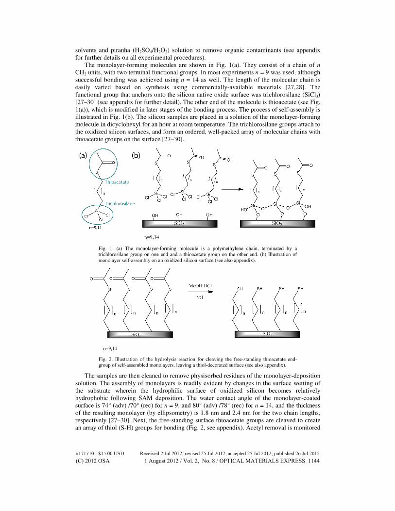
The monolayer-forming molecules are shown in Fig. 1(a). They consist of a chain of n
CH2 units, with two terminal functional groups. In most experiments n = 9 was used, although
successful bonding was achieved using n = 14 as well. The length of the molecular chain is
easily varied based on synthesis using commercially-available materials [27,28]. The
functional group that anchors onto the silicon native oxide surface was trichlorosilane (SiCl3)
[27–30] (see appendix for further detail). The other end of the molecule is thioacetate (see Fig.
1(a)), which is modified in later stages of the bonding process. The process of self-assembly is
illustrated in Fig. 1(b). The silicon samples are placed in a solution of the monolayer-forming
molecule in dicyclohexyl for an hour at room temperature. The trichlorosilane groups attach to
the oxidized silicon surfaces, and form an ordered, well-packed array of molecular chains with
thioacetate groups on the surface [27–30].
Fig. 1. (a) The monolayer-forming molecule is a polymethylene chain, terminated by a
trichlorosilane group on one end and a thioacetate group on the other end. (b) Illustration of
monolayer self-assembly on an oxidized silicon surface (see also appendix).
Fig. 2. Illustration of the hydrolysis reaction for cleaving the free-standing thioacetate end-
group of self-assembled monolayers, leaving a thiol-decorated surface (see also appendix).
The samples are then cleaned to remove physisorbed residues of the monolayer-deposition
solution. The assembly of monolayers is readily evident by changes in the surface wetting of
the substrate wherein the hydrophilic surface of oxidized silicon becomes relatively
hydrophobic following SAM deposition. The water contact angle of the monolayer-coated
surface is 74° (adv) /70° (rec) for n = 9, and 80° (adv) /78° (rec) for n = 14, and the thickness
of the resulting monolayer (by ellipsometry) is 1.8 nm and 2.4 nm for the two chain lengths,
respectively [27–30]. Next, the free-standing surface thioacetate groups are cleaved to create
an array of thiol (S-H) groups for bonding (Fig. 2, see appendix). Acetyl removal is monitored
#171710 - $15.00 USD Received 2 Jul 2012; revised 25 Jul 2012; accepted 25 Jul 2012; published 26 Jul 2012(C) 2012 OSA 1 August 2012 / Vol. 2, No. 8 / OPTICAL MATERIALS EXPRESS 1144

by infra-red spectroscopy based on the disappearance of the characteristic C = O double bond
signal [30,31].
Fig. 3. (a) Bonding a thiol-bearing silicon sample to an InP sample. (b) Bonded InP and silicon
samples. (c) Scanning electron microscope cross-section of bonded samples of InP and silicon,
following cleaving and focused ion beam processing.
Fig. 4. Top-view, infra-red microscopy image of an InP sample and a silicon sample bonded
together. Rings appear in a corner region that was taken from the edge of the InP wafer and
could not be bonded. An illustration of the partially bonded samples is shown to the right of the
microscopy image.
Subsequent processing depends on the specific substrates to be bonded and the two
bonding paradigms that have been pursued. In one case, we have extended the known self-
assembly from solution of alkylthiols onto InP [32,33] to the bonding of a thiol-decorated
silicon substrate to InP, as illustrated in Fig. 3(a). Following a thorough solvent clean and
immersion in HF, an oxide-free InP surface was brought in contact with the thiol-
functionalized-SAM-modified silicon samples (see appendix). The size of the commercially
available InP (100) samples was typically 8 × 8 mm2, and the root-mean-squared micro-
roughness of their surfaces was smaller than 0.2 nm. Bonding of InP to thiol-SAM-coated
silicon was achieved at 120-150 °C for 12-24 hours in a bonding press. Figure 3(b) shows a
bonded pair of samples, and Fig. 3(c) presents a scanning electron microscope (SEM) image
of the cross-section of the bonding interface (made using a focused ion beam). Analysis of
#171710 - $15.00 USD Received 2 Jul 2012; revised 25 Jul 2012; accepted 25 Jul 2012; published 26 Jul 2012(C) 2012 OSA 1 August 2012 / Vol. 2, No. 8 / OPTICAL MATERIALS EXPRESS 1145
high-resolution SEM images of such cross-sections provided an upper limit of 6 nm for the
thickness of the bonding interface (which includes both the silicon oxide and the SAM).
The quality of the bonding was evaluated using infra-red microscopy. Figure 4 shows an
image of the bonding interface between a silicon sample and an InP sample (a different
sample from those shown in Figs. 3(b) and 3(c)). The InP piece was cut out of the edge of the
wafer, so that a region on the right-hand side could not be bonded (see figure). Interferometric
rings are evident in the area that is not bonded, whereas the bonded region is free of such
rings. The image illustrates the formation of a continuous bonded interface in the flat part of
the sample. InP samples taken from the center of the wafer exhibited a uniform bonding
across their entire surface.
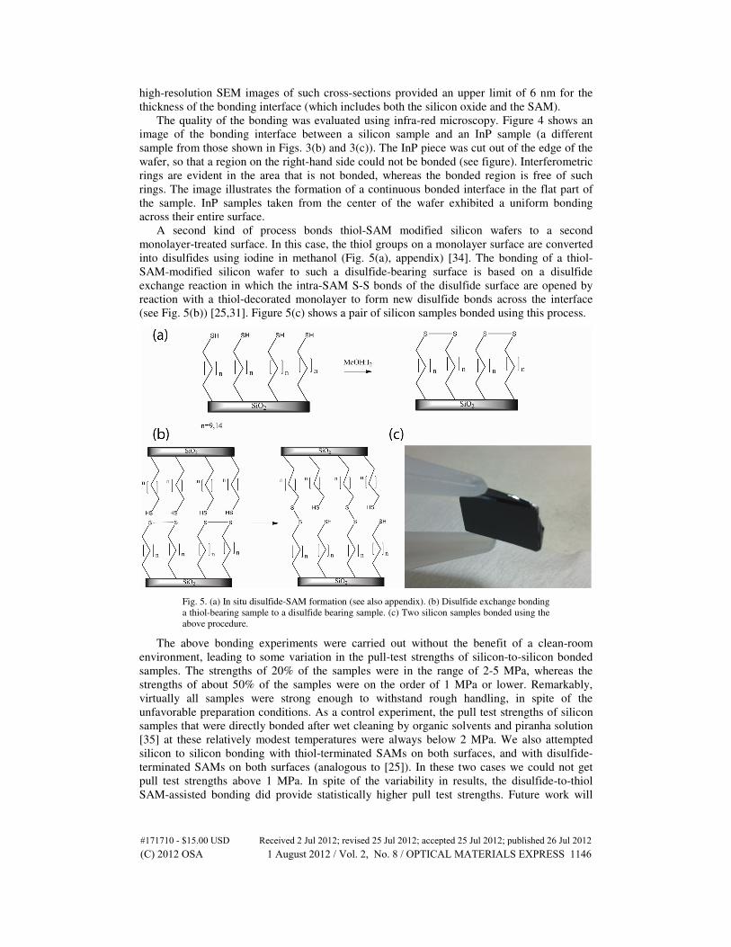
A second kind of process bonds thiol-SAM modified silicon wafers to a second
monolayer-treated surface. In this case, the thiol groups on a monolayer surface are converted
into disulfides using iodine in methanol (Fig. 5(a), appendix) [34]. The bonding of a thiol-
SAM-modified silicon wafer to such a disulfide-bearing surface is based on a disulfide
exchange reaction in which the intra-SAM S-S bonds of the disulfide surface are opened by
reaction with a thiol-decorated monolayer to form new disulfide bonds across the interface
(see Fig. 5(b)) [25,31]. Figure 5(c) shows a pair of silicon samples bonded using this process.
Fig. 5. (a) In situ disulfide-SAM formation (see also appendix). (b) Disulfide exchange bonding
a thiol-bearing sample to a disulfide bearing sample. (c) Two silicon samples bonded using the
above procedure.
The above bonding experiments were carried out without the benefit of a clean-room
environment, leading to some variation in the pull-test strengths of silicon-to-silicon bonded
samples. The strengths of 20% of the samples were in the range of 2-5 MPa, whereas the
strengths of about 50% of the samples were on the order of 1 MPa or lower. Remarkably,
virtually all samples were strong enough to withstand rough handling, in spite of the
unfavorable preparation conditions. As a control experiment, the pull test strengths of silicon
samples that were directly bonded after wet cleaning by organic solvents and piranha solution
[35] at these relatively modest temperatures were always below 2 MPa. We also attempted
silicon to silicon bonding with thiol-terminated SAMs on both surfaces, and with disulfide-
terminated SAMs on both surfaces (analogous to [25]). In these two cases we could not get
pull test strengths above 1 MPa. In spite of the variability in results, the disulfide-to-thiol
SAM-assisted bonding did provide statistically higher pull test strengths. Future work will
#171710 - $15.00 USD Received 2 Jul 2012; revised 25 Jul 2012; accepted 25 Jul 2012; published 26 Jul 2012(C) 2012 OSA 1 August 2012 / Vol. 2, No. 8 / OPTICAL MATERIALS EXPRESS 1146

evaluate the strengths of samples bonded in a clean room environment. We suggest that the
relative hydrophobicity of the SAM treated surface minimizes surface contamination and
combines with the modest flexibility introduced by the monolayer chains to provide a robust,
readily generalizable process.
The pull test strengths of InP bonded to silicon samples reached 2 MPa. The higher end of
the obtained strength values exceeds those in the literature [36]. Here too, virtually all bonded
samples provided handling strength. Further work is necessary to quantify the strength of this
bonding in a controlled environment. Also, the effects on bonding strength of the chain length
of the monolayer-forming molecule, the use of various combinations of thiols and disulfides,
and the bonding temperature, are still under study. In particular, pull test strengths of InP and
silicon samples, directly bonded using oxygen plasma as a control experiment following the
work of Pasquariello and Hjort [37], did reach over 3 MPa.
3. Conclusions
In summary, we have proposed and demonstrated SAM-based wafer bonding between a
monolayer modified surface and a second, bare, substrate and bonding between two
monolayer-modified surfaces. The application of SAMs to the low-temperature bonding of
InP to silicon is particularly important for its potential application in hybrid photonic devices.
We suggest that bonding based on SAMs provides several significant potential advantages: a)
the functional groups at the termini of the monolayer-forming molecules can be adjusted to
accommodate a variety of materials; b) relatively low temperatures are used; c) the disulfide
exchange-based variant of the process is free of outgassing; and d) the few nm-thin bonding
interface could mitigate the surface flatness requirement of direct bonding without disrupting
light transfer. Ongoing work is aimed at the fabrication of hybrid-silicon photonic devices
based on these bonding principles. The robustness and stability of the bonding interface
during operation of active devices remains to be evaluated.
Appendix: experimental procedures
Preparation of silicon samples: Samples were cleaned in chloroform, acetone and ethanol,
blown dry by a flow of filtered nitrogen, and immersed in a mixture of H2SO4 and H2O2 (7:3
ratio) for 20 minutes at 80 °C to remove organic contaminants. The samples were rinsed in
deionized water and blown dry by filtered nitrogen.
Monolayer self-assembly on oxidized silicon surfaces: The monolayer-forming molecules
are prepared by literature procedures [27,28] and mixed with dicyclohexyl (20 µL:10 mL) in a
dried test tube. The samples are put in this solution for 1 hour at room temperature, after
which they are rinsed in chloroform, blown dry under a filtered nitrogen stream, subjected to
ultrasonic cleaning in chloroform for 15 minutes, and blown dry again under a filtered
nitrogen stream. The samples are then cleaned in n-hexane at 80 °C for 6 minutes, rinsed with
room-temperature n-hexane and blown dry with nitrogen.
Cleaving of thioacetate groups: The samples are immersed overnight in a mixture of
hydrochloric acid in methanol (1:9 ratio) at 80 °C, after which they are cleaned using the same
procedure that was applied following monolayer self-assembly.
Conversion of thiol terminated SAMs into disulfide terminated SAMs [31]: The samples
are placed in a solution of iodine (30 mg) in methanol (2 mL) for 15 minutes at room
temperature, and subsequently cleaned as above.
Preparation of InP samples: Samples were cleaned in chloroform, acetone and ethanol,
blown dry by a flow of filtered nitrogen, and immersed in a solution of 4% aqueous
hydrofluoric acid for 10 minutes to remove the native oxide layer. Next, the samples were
rinsed three times in deionized water and blown dry with nitrogen. No further treatment of the
surface was needed. Following the treatment, the InP was quickly pressed against the silicon
sample for bonding in order to avoid oxide re-growth when exposed to air.
#171710 - $15.00 USD Received 2 Jul 2012; revised 25 Jul 2012; accepted 25 Jul 2012; published 26 Jul 2012(C) 2012 OSA 1 August 2012 / Vol. 2, No. 8 / OPTICAL MATERIALS EXPRESS 1147

Bonding: The bonding took place in a stainless steel mechanical fixture. The wafers to be
bonded are pressed against each other inside the fixture and placed in an oven for 24 hours.
The temperatures used were 120 - 150 °C. The fixture is closed with screws until the screw
head is flush against the metal without applying further pressure. Due to the heat in the oven,
the pressure is assumed to be higher than the weight applied.
Pull-Test: A commercial adhesion tester, Defelsko Positest AT-A, was used. The bonded
samples were glued to a metal holder on one side and to a transparent window from the other
side (see Fig. 6). Care was taken to prevent the epoxy from reaching the bonding interface and
affecting the measurement. The strength measurements had an uncertainty of ±0.5 MPa.
Fig. 6. A schematic illustration of the pull-test setup. The bonded wafers are glued to a metallic
holder from one side and to a transparent window from the other side using slow cure epoxy.
Acknowledgments
The work was supported in part by the Israeli Science Foundation (ISF) under grants 635-10
and 1646-08; by the 'TERA SANTA' MAGNET consortium of the Office of the Chief
Scientist, the Israeli Ministry of Industry, Trade and Labor; and by the Edward and Judith
Steinberg Chair in Nanotechnology, Bar-Ilan University.
#171710 - $15.00 USD Received 2 Jul 2012; revised 25 Jul 2012; accepted 25 Jul 2012; published 26 Jul 2012(C) 2012 OSA 1 August 2012 / Vol. 2, No. 8 / OPTICAL MATERIALS EXPRESS 1148
Related Documents
![Self-Assembled Si(111) Surface States: 2D Dirac Material ...fliu/pdfs/PhysRevLett.115.026803.pdf · 1=3 monolayer halogen coverage. ... more power-efficient circuitry. ... [11,12].](https://static.cupdf.com/doc/110x72/5cc64a9488c9936f738c9fd3/self-assembled-si111-surface-states-2d-dirac-material-fliupdfsphysrevlett115026803pdf.jpg)


