Monolayer coverage and channel length set the mobility in self-assembled monolayer field-effect transistors Simon G. J. Mathijssen 1,2 , Edsger C. P. Smits 1,3 , Paul A. van Hal 1 , Harry J. Wondergem 1 , Sergei A. Ponomarenko 4 , Armin Moser 5 , Roland Resel 5 , Peter A. Bobbert 2 , Martijn Kemerink 2 , Rene ´ A. J. Janssen 2 and Dago M. de Leeuw 1,6 * The mobility of self-assembled monolayer field-effect transistors (SAMFETs) traditionally decreases dramatically with increasing channel length. Recently, however, SAMFETs using liquid-crystalline molecules have been shown to have bulk-like mobilities that are virtually independent of channel length. Here, we reconcile these scaling relations by showing that the mobility in liquid crystalline SAMFETs depends exponentially on the channel length only when the monolayer is incomplete. We explain this dependence both numerically and analytically, and show that charge transport is not affected by carrier injection, grain boundaries or conducting island size. At partial coverage, that is when the monolayer is incomplete, liquid- crystalline SAMFETs thus form a unique model system to study size-dependent conductance originating from charge percolation in two dimensions. C harge carriers in a field-effect transistor are injected from the source contact, transported through the semiconductor, then collected at the drain contact. The carriers are confined by the gate field as a thin accumulation layer at the semiconductor–gate dielectric interface 1 . In a monolayer transistor the semiconductor consists of only a single sheet of molecules, and the layer thickness is comparable to that of the accumulation layer. Electrical transport is then, by definition, two-dimensional, so any structural imper- fections such as voids or grain boundaries lead to potential barriers and, hence, to a deterioration in charge carrier mobility 2,3 . A prerequisite for efficient charge transport is long-range con- nectivity, and to form a conducting path between the source and drain electrode, the molecules should be intimately connected. In addition, the nature of the electrical contact is crucial. Historically, connecting an effective injecting electrode to a single layer of molecules has proven to be a challenge 4 , and the extracted mobility in monolayer transistors is often orders of magnitude lower than that in corresponding bulk thin-film transistors due to injection-limited contacts 5–7 . Self-assembled 8 monolayer transistors in which the semiconduc- tor is a monolayer spontaneously formed on the gate dielectric, tra- ditionally show inverse scaling; that is, device mobility decreases dramatically with increasing channel length. Only sub-micrometre channels have shown a gate-dependent source–drain current, with the mobility in longer channels being negligible 4 . Recently, however, we have demonstrated self-assembled monolayer field- effect transistors (SAMFETs) in which the extracted device mobility is virtually independent of channel length 9 . To investigate this contradiction in the scaling of the mobility, we present a technology to fabricate SAMFETs with varying monolayer coverage and channel lengths. By ensuring both proper charge carrier injection and an ordered SAM microstructure, this technology allows the charge transport in a two-dimensional percolating semiconductor network to be systematically probed. For sub-monolayer coverage, the anomalous inverse scaling behaviour reported previously for SAMFETs is reproduced and can be accounted for by numerical and analytical percolation models. SAMFETs 9 of varying coverage were prepared on heavily doped silicon wafers (acting as the common gate) covered with a 200-nm layer of thermally grown SiO 2 . The gold source and drain contacts were defined by conventional photolithography and wet etchant chemistry. Titanium (10 nm) was used as an adhesion layer. The liquid-crystalline active molecule comprised a mesogenic quinque- thiophene core, end-capped with an ethyl group to enhance stability and solubility. To bind the molecule to the SiO 2 gate di- electric, a monochlorosilane anchoring group was attached via an undecane spacer. The chemical structure of the self-assembling mol- ecule, chloro[11-(5 0000 -ethyl-2,2 0 :5 0 ,2 00 :5 00 ,2 000 :5 000 ,2 0000 -quinquethien-5-yl) undecyl]-dimethylsilane is shown in the inset to Fig. 1. To induce self- assembly of the molecules, the SiO 2 gate dielectric was activated by an oxygen plasma treatment followed by acid hydrolysis. The SAM was then formed by submerging the substrate in a dry toluene solution of the semiconducting molecule. The coverage was varied by changing the immersion time in the solution from 15 min to 30 min, 1 h and 15 h. Typical topography images (20 20 mm 2 ) are presented in Fig. 1a–d. It is clear that the SAM grows in the form of islands, with coverage varying from 0.05+0.05, 0.31+0.08, 0.5+0.1 to 1, respectively, depending on the immersion time. Note that the height difference in the topography is 3.5 nm, in perfect agreement with the calculated length of the molecule. A small fraction of the monolayer is a bilayer, most likely due to the formation of dimers in the solution. 1 Philips Research Laboratories, High Tech Campus 4, 5656 AE Eindhoven, The Netherlands, 2 Department of Applied Physics, Eindhoven University of Technology, PO Box 513, 5600 MB Eindhoven, The Netherlands, 3 Holst Centre/TNO, High Tech Campus 34, 5656 AE Eindhoven, The Netherlands, 4 Enikolopov Institute of Synthetic Polymer Materials of Russian Academy of Sciences, Profsoyuznaya 70, 117393 Moscow, Russia, 5 Institute of Solid State Physics, Graz University of Technology, Petersgasse 16A, 8010 Graz, Austria, 6 Molecular Electronics, Zernike Institute for Advanced Materials, University of Groningen, Nijenborgh 4, 9747 AG Groningen, The Netherlands. *e-mail: [email protected] ARTICLES PUBLISHED ONLINE: 9 AUGUST 2009 | DOI: 10.1038/NNANO.2009.201 NATURE NANOTECHNOLOGY | VOL 4 | OCTOBER 2009 | www.nature.com/naturenanotechnology 674 © 2009 Macmillan Publishers Limited. All rights reserved.

Welcome message from author
This document is posted to help you gain knowledge. Please leave a comment to let me know what you think about it! Share it to your friends and learn new things together.
Transcript

Monolayer coverage and channel length set themobility in self-assembled monolayer field-effecttransistorsSimon G. J. Mathijssen1,2, Edsger C. P. Smits1,3, Paul A. van Hal1, Harry J. Wondergem1,
Sergei A. Ponomarenko4, Armin Moser5, Roland Resel5, Peter A. Bobbert2, Martijn Kemerink2,
Rene A. J. Janssen2 and Dago M. de Leeuw1,6*
The mobility of self-assembled monolayer field-effect transistors (SAMFETs) traditionally decreases dramatically withincreasing channel length. Recently, however, SAMFETs using liquid-crystalline molecules have been shown to have bulk-likemobilities that are virtually independent of channel length. Here, we reconcile these scaling relations by showing that themobility in liquid crystalline SAMFETs depends exponentially on the channel length only when the monolayer is incomplete.We explain this dependence both numerically and analytically, and show that charge transport is not affected by carrierinjection, grain boundaries or conducting island size. At partial coverage, that is when the monolayer is incomplete, liquid-crystalline SAMFETs thus form a unique model system to study size-dependent conductance originating from chargepercolation in two dimensions.
Charge carriers in a field-effect transistor are injected from thesource contact, transported through the semiconductor, thencollected at the drain contact. The carriers are confined by the
gate field as a thin accumulation layer at the semiconductor–gatedielectric interface1. In a monolayer transistor the semiconductorconsists of only a single sheet of molecules, and the layer thicknessis comparable to that of the accumulation layer. Electrical transportis then, by definition, two-dimensional, so any structural imper-fections such as voids or grain boundaries lead to potentialbarriers and, hence, to a deterioration in charge carrier mobility2,3.A prerequisite for efficient charge transport is long-range con-nectivity, and to form a conducting path between the source anddrain electrode, the molecules should be intimately connected.In addition, the nature of the electrical contact is crucial.Historically, connecting an effective injecting electrode to a singlelayer of molecules has proven to be a challenge4, and the extractedmobility in monolayer transistors is often orders of magnitudelower than that in corresponding bulk thin-film transistors due toinjection-limited contacts5–7.
Self-assembled8 monolayer transistors in which the semiconduc-tor is a monolayer spontaneously formed on the gate dielectric, tra-ditionally show inverse scaling; that is, device mobility decreasesdramatically with increasing channel length. Only sub-micrometrechannels have shown a gate-dependent source–drain current, withthe mobility in longer channels being negligible4. Recently,however, we have demonstrated self-assembled monolayer field-effect transistors (SAMFETs) in which the extracted device mobilityis virtually independent of channel length9. To investigate thiscontradiction in the scaling of the mobility, we present a technologyto fabricate SAMFETs with varying monolayer coverage andchannel lengths. By ensuring both proper charge carrier injection
and an ordered SAM microstructure, this technology allows thecharge transport in a two-dimensional percolating semiconductornetwork to be systematically probed. For sub-monolayer coverage,the anomalous inverse scaling behaviour reported previously forSAMFETs is reproduced and can be accounted for by numericaland analytical percolation models.
SAMFETs9 of varying coverage were prepared on heavily dopedsilicon wafers (acting as the common gate) covered with a 200-nmlayer of thermally grown SiO2. The gold source and drain contactswere defined by conventional photolithography and wet etchantchemistry. Titanium (10 nm) was used as an adhesion layer. Theliquid-crystalline active molecule comprised a mesogenic quinque-thiophene core, end-capped with an ethyl group to enhancestability and solubility. To bind the molecule to the SiO2 gate di-electric, a monochlorosilane anchoring group was attached via anundecane spacer. The chemical structure of the self-assembling mol-ecule, chloro[11-(50000-ethyl-2,20:50,200:500,2000:5000,20000-quinquethien-5-yl)undecyl]-dimethylsilane is shown in the inset to Fig. 1. To induce self-assembly of the molecules, the SiO2 gate dielectric was activated by anoxygen plasma treatment followed by acid hydrolysis. The SAM wasthen formed by submerging the substrate in a dry toluene solution ofthe semiconducting molecule. The coverage was varied by changingthe immersion time in the solution from 15 min to 30 min, 1 h and 15 h.
Typical topography images (20� 20 mm2) are presented inFig. 1a–d. It is clear that the SAM grows in the form of islands,with coverage varying from 0.05+0.05, 0.31+0.08, 0.5+0.1 to 1,respectively, depending on the immersion time. Note that theheight difference in the topography is 3.5 nm, in perfect agreementwith the calculated length of the molecule. A small fraction of themonolayer is a bilayer, most likely due to the formation of dimersin the solution.
1Philips Research Laboratories, High Tech Campus 4, 5656 AE Eindhoven, The Netherlands, 2Department of Applied Physics, Eindhoven University ofTechnology, PO Box 513, 5600 MB Eindhoven, The Netherlands, 3Holst Centre/TNO, High Tech Campus 34, 5656 AE Eindhoven, The Netherlands,4Enikolopov Institute of Synthetic Polymer Materials of Russian Academy of Sciences, Profsoyuznaya 70, 117393 Moscow, Russia, 5Institute of Solid StatePhysics, Graz University of Technology, Petersgasse 16A, 8010 Graz, Austria, 6Molecular Electronics, Zernike Institute for Advanced Materials, University ofGroningen, Nijenborgh 4, 9747 AG Groningen, The Netherlands. *e-mail: [email protected]
ARTICLESPUBLISHED ONLINE: 9 AUGUST 2009 | DOI: 10.1038/NNANO.2009.201
NATURE NANOTECHNOLOGY | VOL 4 | OCTOBER 2009 | www.nature.com/naturenanotechnology674
© 2009 Macmillan Publishers Limited. All rights reserved.

A prerequisite to transport charges in self-assembled monolayersis long-range order. Self-assembled monolayers of alkanethiols ongold grow dynamically, and a perfectly ordered SAM is onlyobtained when the coverage is close to 100% (ref. 10). In contrastto alkanethiol monolayer formation on gold, the assembly ofsilanes on SiO2 is far less reversible and the SAM grows throughthe development of islands11. In the present case, the self-assem-bling molecule consists of an aliphatic chain and a thiophenecore, each having the capability to drive the self-assembly process.To obtain efficient charge transport, the thiophene units shouldbe long-range ordered. The microstructure of the partially coveredSAMs was determined from grazing incidence diffraction measure-ments. The diffracted intensity is presented as a colour map in Fig. 2as a function of perpendicular and in-plane scattering vectors, qzand qxy. The horizontal line at low qz is due to diffuse scatteringfrom the sample surface at the critical angle as described byothers12. Most important are the vertical lines, the so-called Braggrods. They demonstrate in-plane order arising from the thiopheneunits; the rod shape results from the absence of periodicity perpen-dicular to the islands. The onset of the Bragg rods directly at theYoneda line reveals that the thiophene units are oriented perpen-dicular to the substrate surface and packed in a herringbone struc-ture (see Supplementary Information). The grazing incidencediffraction measurements show that the SAM grows in long-rangeordered, crystalline islands.
Si
S
S
S
S
S
a b
c d
Cl
Figure 1 | SAM growth. a–d, Typical topography images (20� 20mm2) of partially covered SAMFETs measured with AFM. The immersion time was varied
from 15 min (a) to 30 min (b), 1 h (c) and 15 h (d), with coverage obtained as average values over six measurements, and equalling 0.05+0.05, 0.31+0.08,
0.5+0.1 and 1, respectively. The inset to a shows the chemical structure of the self-assembling molecule.
0.3
0.25
0.2
0.15
0.1
0.05
01.2 1.4 1.6 1.8 2
qxy (Å−1)
q z (Å
−1)
Figure 2 | SAM microstructure. Diffraction pattern from a partially covered
SAM obtained with grazing incidence X-ray diffraction measurements. The
diffracted intensity is presented as a function of the out-of-plane and in-plane
scattering vectors qz and qxy. The Bragg rods at in-plane scattering vectors of
1.393, 1.605 and 1.968 Å21 indicate an in-plane crystalline order within the
islands of the incomplete SAM. The rods can be indexed as the (1.1), (0.2)
and (1.2) reflections of a rectangular unit cell with lattice constants of 5.49
and 7.83 Å, demonstrating order in the partially covered SAM.
NATURE NANOTECHNOLOGY DOI: 10.1038/NNANO.2009.201 ARTICLES
NATURE NANOTECHNOLOGY | VOL 4 | OCTOBER 2009 | www.nature.com/naturenanotechnology 675
© 2009 Macmillan Publishers Limited. All rights reserved.
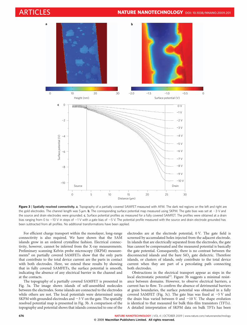
For efficient charge transport within the monolayer, long-rangeconnectivity is also required. We have shown that the SAMislands grow in an ordered crystalline fashion. Electrical connec-tivity, however, cannot be inferred from the X-ray measurements.Preliminary scanning Kelvin probe microscopy (SKPM) measure-ments9 on partially covered SAMFETs show that the only partsthat contribute to the total device current are the parts in contactwith both electrodes. Here, we extend these results by showingthat in fully covered SAMFETs, the surface potential is smooth,indicating the absence of any electrical barrier in the channel andat the contacts.
The topography of a partially covered SAMFET is presented inFig. 3a. The image shows islands of self-assembled moleculesbetween the electrodes. Some islands are connected to the electrodeswhile others are not. The local potentials were determined usingSKPM with grounded electrodes and 23 V on the gate. The spatiallyresolved potential map is presented in Fig. 3b. A comparison of thetopography and potential shows that islands connected to one of the
electrodes are at the electrode potential, 0 V. The gate field isscreened by accumulated holes injected from the adjacent electrode.In islands that are electrically separated from the electrodes, the gatebias cannot be compensated and the measured potential is basicallythe gate potential. Consequently, there is no contrast between thedisconnected islands and the bare SiO2 gate dielectric. Thereforeislands, or clusters of islands, only contribute to the total devicecurrent when they are part of a percolating path connectingboth electrodes.
Obstructions in the electrical transport appear as steps in thelocal electrostatic potential13. Figure 3b suggests a minimal resist-ance between domains. However, to observe electrical barriers, acurrent has to flow. To confirm the absence of detrimental barriersat grain boundaries, the surface potential was obtained in a fullycovered SAMFET (Fig. 3c). The gate bias was fixed at 25 V andthe drain bias varied between 0 and 210 V. The shape evolutionis identical to that measured for bulk thin-film transistors (TFTs).A detailed interpretation of SKPM data on bulk TFTs has been
0
0
−2
−4
−6
−8
−10−10 V
−9 V
−8 V
−7 V
−6 V
−5 V
−4 V
−3 V
−2 V
−1 V
0 V
0
Source Drain
5 10 15 20 25 30Distance (µm)
Surfa
ce p
oten
tial (
V)
10Height (nm) Surface potential (V)
20 30 −2.0 −1.5 −1.0 −0.5 0
a b
c
Figure 3 | Spatially resolved connectivity. a, Topography of a partially covered SAMFET measured with AFM. The dark red regions on the left and right are
the gold electrodes. The channel length was 5 mm. b, The corresponding surface potential map measured using SKPM. The gate bias was set at 23 V and
the source and drain electrodes were grounded. c, Surface potential profiles as measured for a fully covered SAMFET. The profiles were obtained at a drain
bias ranging from 0 to 210 V in steps of 21 V with a gate bias of 25 V. The potential profile measured with the source and drain electrode grounded has
been subtracted from all profiles. No additional transformations have been applied.
ARTICLES NATURE NANOTECHNOLOGY DOI: 10.1038/NNANO.2009.201
NATURE NANOTECHNOLOGY | VOL 4 | OCTOBER 2009 | www.nature.com/naturenanotechnology676
© 2009 Macmillan Publishers Limited. All rights reserved.
presented elsewhere14. Here, we emphasize the smoothness of thepotential. The absence of steps indicates that the SAM is homoge-neously conductive. Imperfections such as grain boundaries orvoids could not be identified. The electrical connection betweengrains, possibly with different crystallographic orientations, is there-fore perfect. Note also that the surface potential is smooth even atthe contacts, indicating that the contact resistance is small13.
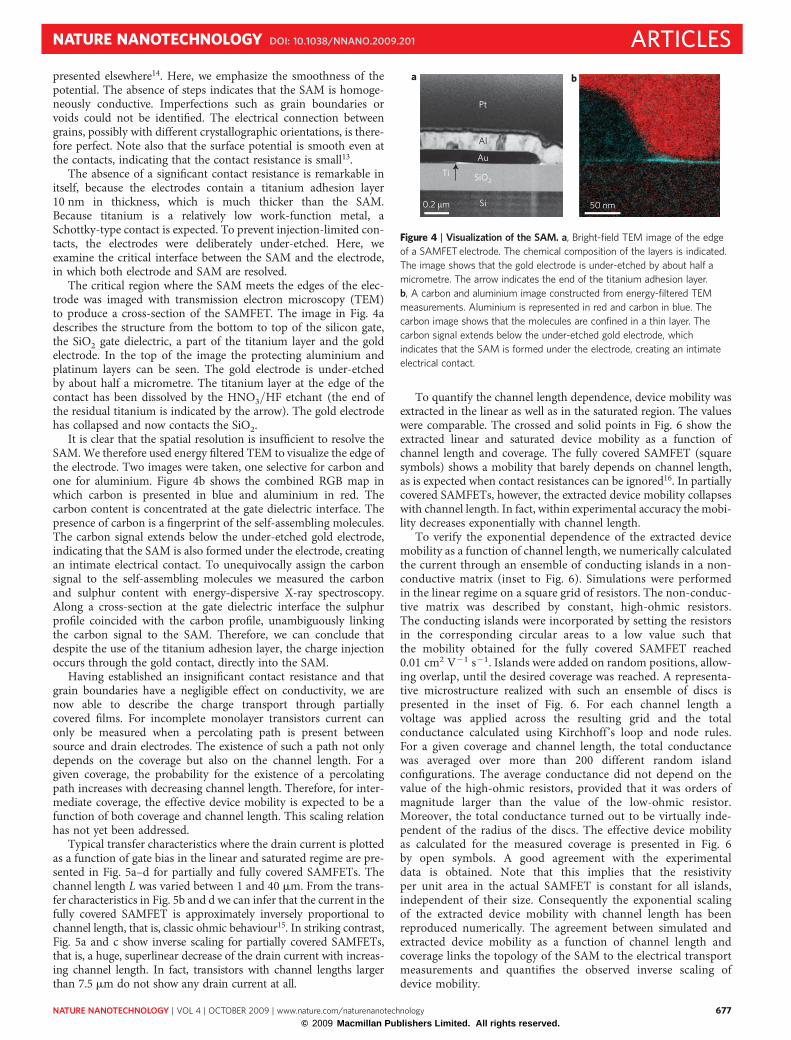
The absence of a significant contact resistance is remarkable initself, because the electrodes contain a titanium adhesion layer10 nm in thickness, which is much thicker than the SAM.Because titanium is a relatively low work-function metal, aSchottky-type contact is expected. To prevent injection-limited con-tacts, the electrodes were deliberately under-etched. Here, weexamine the critical interface between the SAM and the electrode,in which both electrode and SAM are resolved.
The critical region where the SAM meets the edges of the elec-trode was imaged with transmission electron microscopy (TEM)to produce a cross-section of the SAMFET. The image in Fig. 4adescribes the structure from the bottom to top of the silicon gate,the SiO2 gate dielectric, a part of the titanium layer and the goldelectrode. In the top of the image the protecting aluminium andplatinum layers can be seen. The gold electrode is under-etchedby about half a micrometre. The titanium layer at the edge of thecontact has been dissolved by the HNO3/HF etchant (the end ofthe residual titanium is indicated by the arrow). The gold electrodehas collapsed and now contacts the SiO2.
It is clear that the spatial resolution is insufficient to resolve theSAM. We therefore used energy filtered TEM to visualize the edge ofthe electrode. Two images were taken, one selective for carbon andone for aluminium. Figure 4b shows the combined RGB map inwhich carbon is presented in blue and aluminium in red. Thecarbon content is concentrated at the gate dielectric interface. Thepresence of carbon is a fingerprint of the self-assembling molecules.The carbon signal extends below the under-etched gold electrode,indicating that the SAM is also formed under the electrode, creatingan intimate electrical contact. To unequivocally assign the carbonsignal to the self-assembling molecules we measured the carbonand sulphur content with energy-dispersive X-ray spectroscopy.Along a cross-section at the gate dielectric interface the sulphurprofile coincided with the carbon profile, unambiguously linkingthe carbon signal to the SAM. Therefore, we can conclude thatdespite the use of the titanium adhesion layer, the charge injectionoccurs through the gold contact, directly into the SAM.
Having established an insignificant contact resistance and thatgrain boundaries have a negligible effect on conductivity, we arenow able to describe the charge transport through partiallycovered films. For incomplete monolayer transistors current canonly be measured when a percolating path is present betweensource and drain electrodes. The existence of such a path not onlydepends on the coverage but also on the channel length. For agiven coverage, the probability for the existence of a percolatingpath increases with decreasing channel length. Therefore, for inter-mediate coverage, the effective device mobility is expected to be afunction of both coverage and channel length. This scaling relationhas not yet been addressed.
Typical transfer characteristics where the drain current is plottedas a function of gate bias in the linear and saturated regime are pre-sented in Fig. 5a–d for partially and fully covered SAMFETs. Thechannel length L was varied between 1 and 40 mm. From the trans-fer characteristics in Fig. 5b and d we can infer that the current in thefully covered SAMFET is approximately inversely proportional tochannel length, that is, classic ohmic behaviour15. In striking contrast,Fig. 5a and c show inverse scaling for partially covered SAMFETs,that is, a huge, superlinear decrease of the drain current with increas-ing channel length. In fact, transistors with channel lengths largerthan 7.5 mm do not show any drain current at all.
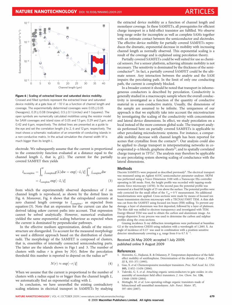
To quantify the channel length dependence, device mobility wasextracted in the linear as well as in the saturated region. The valueswere comparable. The crossed and solid points in Fig. 6 show theextracted linear and saturated device mobility as a function ofchannel length and coverage. The fully covered SAMFET (squaresymbols) shows a mobility that barely depends on channel length,as is expected when contact resistances can be ignored16. In partiallycovered SAMFETs, however, the extracted device mobility collapseswith channel length. In fact, within experimental accuracy the mobi-lity decreases exponentially with channel length.
To verify the exponential dependence of the extracted devicemobility as a function of channel length, we numerically calculatedthe current through an ensemble of conducting islands in a non-conductive matrix (inset to Fig. 6). Simulations were performedin the linear regime on a square grid of resistors. The non-conduc-tive matrix was described by constant, high-ohmic resistors.The conducting islands were incorporated by setting the resistorsin the corresponding circular areas to a low value such thatthe mobility obtained for the fully covered SAMFET reached0.01 cm2 V21 s21. Islands were added on random positions, allow-ing overlap, until the desired coverage was reached. A representa-tive microstructure realized with such an ensemble of discs ispresented in the inset of Fig. 6. For each channel length avoltage was applied across the resulting grid and the totalconductance calculated using Kirchhoff’s loop and node rules.For a given coverage and channel length, the total conductancewas averaged over more than 200 different random islandconfigurations. The average conductance did not depend on thevalue of the high-ohmic resistors, provided that it was orders ofmagnitude larger than the value of the low-ohmic resistor.Moreover, the total conductance turned out to be virtually inde-pendent of the radius of the discs. The effective device mobilityas calculated for the measured coverage is presented in Fig. 6by open symbols. A good agreement with the experimentaldata is obtained. Note that this implies that the resistivityper unit area in the actual SAMFET is constant for all islands,independent of their size. Consequently the exponential scalingof the extracted device mobility with channel length has beenreproduced numerically. The agreement between simulated andextracted device mobility as a function of channel length andcoverage links the topology of the SAM to the electrical transportmeasurements and quantifies the observed inverse scaling ofdevice mobility.
ba
0.2 µm 50 nm
Pt
Si
SiO2Ti
Au
Al
Figure 4 | Visualization of the SAM. a, Bright-field TEM image of the edge
of a SAMFET electrode. The chemical composition of the layers is indicated.
The image shows that the gold electrode is under-etched by about half a
micrometre. The arrow indicates the end of the titanium adhesion layer.
b, A carbon and aluminium image constructed from energy-filtered TEM
measurements. Aluminium is represented in red and carbon in blue. The
carbon image shows that the molecules are confined in a thin layer. The
carbon signal extends below the under-etched gold electrode, which
indicates that the SAM is formed under the electrode, creating an intimate
electrical contact.
NATURE NANOTECHNOLOGY DOI: 10.1038/NNANO.2009.201 ARTICLES
NATURE NANOTECHNOLOGY | VOL 4 | OCTOBER 2009 | www.nature.com/naturenanotechnology 677
© 2009 Macmillan Publishers Limited. All rights reserved.

In the following we further rationalize this exponential dependenceusing two approaches. The first method is based on the connectivityfunction. The alternative approach incorporates the measured mor-phology when applying a cluster radius distribution argument. Bothmethodologies yield an exponential scaling of mobility withchannel length.
We describe the microstructure by an effective medium17. In thisapproximation the simulated SAM is disentangled and randomlyredistributed over a lattice while keeping the coverage fixed. Pointsthat are intimately connected form clusters. The probability thattwo individual points separated by a distance x belong to thesame cluster is then given by the connectivity function g(x):18
gðxÞ ¼ exp � xjð pÞ
� �ð1Þ
where the correlation length j is a function of the coverage p. Notethat the functional dependence of j on p has been studied in greatdetail19, but here only the exponential dependence of g on x isimportant. For a fully covered SAMFET the correlation length isinfinite, and hence the connectivity function is unity. In this case,the source and drain electrode belong to the same and onlycluster. The current is then given by15
Icomplete ¼ðW
0jcompletedw ð2Þ
where jcomplete is the current density per unit length and the inte-gration is over the channel width W. For an incomplete SAMFETwe conjecture that the major contribution to the current comesfrom paths connected perpendicularly between source and drain
10−5
10−7
10−9
10−11
10−13
10−15
−20 −10 0 10Gate voltage (V)
Channel length1 µm 2 µm 5 µm 7.5 µm
Channel length1 µm 2 µm 5 µm 7.5 µm 10 µm 20 µm 40 µm
Partially covered Fully covered
Partially covered Fully covered
−Dra
in c
urre
nt (A
)
10−5
10−7
10−9
10−11
10−13
10−15
−20 −10 0 10Gate voltage (V)
−Dra
in c
urre
nt (A
)
10−5
10−7
10−9
10−11
10−13
10−15
−20 −10 0 10Gate voltage (V)
−Dra
in c
urre
nt (A
)
10−5
10−7
10−9
10−11
10−13
10−15
−20 −10 0 10Gate voltage (V)
−Dra
in c
urre
nt (A
)
Channel length1 µm 2 µm 5 µm 7.5 µm
Channel length1 µm 2 µm 5 µm 7.5 µm 10 µm 20 µm 40 µm
a b
c d
Figure 5 | Electrical transport versus monolayer coverage. a,b, Transfer characteristics of SAMFETs in which the drain current at a drain bias of 22 V is
presented as a function of gate bias for a partially and fully covered SAMFET, respectively. c,d, The drain currents at a drain bias of 220 V. The channel
length L was varied between 1 and 40 mm. Partially covered SAMFETs with channel lengths larger than 7.5 mm do not show any drain current at all.
ARTICLES NATURE NANOTECHNOLOGY DOI: 10.1038/NNANO.2009.201
NATURE NANOTECHNOLOGY | VOL 4 | OCTOBER 2009 | www.nature.com/naturenanotechnology678
© 2009 Macmillan Publishers Limited. All rights reserved.
electrode. We subsequently assume that the current is proportionalto the connectivity function evaluated at a distance equal to thechannel length L, that is, g(L). The current for the partiallycovered SAMFET then yields
Iincomplete ¼ðW
0jcompletegðLÞdw ¼ exp½�L=j�
ðW
0jcompletedw
¼ Icomplete exp½�L=j� ð3Þ
from which the experimentally observed dependence of I onchannel length is reproduced, as shown by the dotted lines inFig. 6. Moreover, Fig. 6 shows that the extrapolated currents atzero channel length converge to Icomplete, as expected fromequation (3). Note that an expression for the current can also bederived taking askew current paths into account. That expressioncannot be solved analytically. However, numerical evaluationyielded the same exponential scaling behaviour as expected whenthe current is dominated by perpendicular pathways.
In the effective medium approximation, details of the micro-structure are disregarded. To account for the measured morphologywe used a different approach based on the distribution of clusterradii. The morphology of the SAMFET is composed of clusters,that is, ensembles of internally connected semiconducting parts.The latter are the islands shown in Figs 1 and 3. The number ofclusters with radius r is given by N(r). Below the percolationthreshold this number is reported to depend on the radius as20
NðrÞ � exp½�r=j� ð4Þ
When we assume that the current is proportional to the number ofclusters with a radius equal to or bigger than the channel length L,we automatically find an exponential scaling with L.
In conclusion, we have unravelled the existing contradictoryscaling relations in electrical transport in SAMFETs by studying
the extracted device mobility as a function of channel length andmonolayer coverage. In these SAMFETs, all prerequisites for efficientcharge transport in a field-effect transistor are fulfilled. We observelong-range order for incomplete as well as complete SAMs togetherwith an intimate contact between the semiconductor and electrodes.The effective device mobility for partially covered SAMFETs repro-duces the dramatic, exponential decrease in mobility with increasingchannel length as normally observed. This exponential scaling is aresult of the coverage and is explained using percolation theory.
Partially covered SAMFETs could be well suited for use as chemi-cal sensors. For a sensor platform, achieving ultimate mobility is notnecessary. The sensitivity is dominated by the thickness of the semi-conductor21. In fact, a partially covered SAMFET could be the ulti-mate sensor. Any interaction between the analyte and the SAMimpairs the percolating path. In the limit of only one conductingpath, the current is completely blocked.
In a broader context it should be noted that transport in inhomo-geneous conductors is described by percolation. Conductivity isgenerally studied in a macroscopic sample where the overall conduc-tivity is investigated as a function of the quantity of conductivematerial in a non-conductive matrix. Usually, the dimensions ofthe sample are assumed to be infinite. The uniqueness of ourapproach is that we explicitly take into account the microstructureby investigating the scaling of the conductivity with concentrationand lateral device dimensions. In effect, we study percolation on alocal instead of the more common global scale. The transport analy-sis performed here on partially covered SAMFETs is applicable toother percolating microelectronic systems. For instance, a compar-able mobility decrease with channel length has been reported foracenes that crystallize from the contacts22. Our analysis could alsobe applied to charge transport in interpenetrating networks in co-evaporated p–n blends, graphene sheets23, and to spatially correlatedcharge transport in TFTs5. The analysis may therefore be applicableto any percolating system showing scaling of conductance with thelateral dimensions.
MethodsDiscrete SAMFETs were prepared as described previously9. The electrical transportwas measured using an Agilent 4155C semiconductor parameter analyser. SKPMwas performed using a Veeco Dimension 3100 with a Nanoscope IIIa controlleroperating in lift mode. First, the height profile was recorded with tapping-modeatomic force microscopy (AFM). In the second pass the potential profile wasmeasured at a fixed lift height of 25 nm above the surface. The potential profiles wereonly corrected for the small offset of the Vsd¼ 0 V measurement. No additionaltransformations were applied. Cross-sections were made by means of focused ionbeam transmission electron microscopy with a TECNAI F30ST TEM. A thin slabwas cut from the SAMFET using focused ion beam (FIB) milling. To prevent anydamage, a layer of aluminium was first deposited, followed by a layer of platinum.The thin slab was milled to electron transparency and investigated with TEM.Energy-filtered TEM was used to obtain the carbon and aluminium image. Anenergy-dispersive X-ray process was used to determine the carbon and sulphurprofiles along the cross-sections.
Grazing incidence X-ray diffraction investigations were performed at beamlineG2 at the synchrotron CHESS using radiation with a wavelength of 1.2681 Å. Anangle of incidence of 0.138 was used in combination with a position-sensitivedetector simultaneously covering a qz range from 0 to 0.7 Å21.
Received 26 May 2009; accepted 1 July 2009;published online 9 August 2009
References1. Horowitz, G., Hajlaoui, R. & Delannoy, P. Temperature dependence of the field-
effect mobility of sexithiophene. Determination of the density of traps. J. Phys.III 5, 355–371 (1995).
2. Guo, X. et al. Chemoresponsive monolayer transistors. Proc. Natl Acad. Sci. USA103, 11452–11456 (2006).
3. Tulevski, G. S. et al. Attaching organic semiconductors to gate oxides: in situassembly of monolayer field effect transistors. J. Am. Chem. Soc. 126,15048–15050 (2004).
4. Mottaghi, M. et al. Low-operating-voltage organic transistors made ofbifunctional self-assembled monolayers. Adv. Funct. Mater. 17,597–604 (2007).
10−2
10−3
10−4
10−5
Channel length (µm)
Extr
acte
d de
vice
mob
ility
(cm
2 V
−1 s−1
)
0 5 10 15 20 25 30 35 40
Figure 6 | Scaling of extracted linear and saturated device mobility.
Crossed and filled symbols represent the extracted linear and saturated
device mobility at a gate bias of 210 V as a function of channel length and
coverage. The experimentally determined coverages were 0.05+0.05
(hexagons), 0.31+0.08 (triangles), 0.5+0.1 (circles) and 1 (squares). The
open symbols are numerically calculated mobilities using the resistor model
for SAM coverages and island sizes of 0.05 and 1.5 mm, 0.29 and 2 mm, and
0.42 and 6 mm, respectively. The dotted lines are presented as a guide to
the eye and set the correlation length j to 2, 6 and 12mm, respectively. The
inset shows a schematic realization of an ensemble of conducting islands in
a non-conductive matrix. In the actual simulation the channel width W is
much bigger than its length L.
NATURE NANOTECHNOLOGY DOI: 10.1038/NNANO.2009.201 ARTICLES
NATURE NANOTECHNOLOGY | VOL 4 | OCTOBER 2009 | www.nature.com/naturenanotechnology 679
© 2009 Macmillan Publishers Limited. All rights reserved.

5. Dinelli, F. et al. Spatially correlated charge transport in organic thin filmtransistors. Phys. Rev. Lett. 92, 116802 (2004).
6. Ruiz, R., Papadimitratos, A., Mayer, A. C. & Malliaras, G. G. Thicknessdependence of mobility in pentacene thin-film transistors. Adv. Mater. 17,1795–1798 (2005).
7. Park, B.-N., Seo, S. & Evans, P. G. Channel formation in single-monolayerpentacene thin film transistors. J. Phys. D 40, 3506–3511 (2007).
8. Whitesides, G. M. & Grzybowski, B. Self-assembly at all scales. Science 295,2418–2421 (2002).
9. Smits, E. C. P. et al. Bottom-up organic integrated circuits. Nature 455,956–959 (2008).
10. Yang G. & Liu, G.-Y. New insights for self-assembled monolayers oforganothiols on Au(111) revealed by scanning tunneling microscopy. J. Phys.Chem. B 107, 8746–8759 (2003).
11. Onclin, S., Ravoo, B. J. & Reinhoudt, D. N. Engineering silicon oxide surfacesusing self-assembled monolayers. Angew. Chem. Int. Ed. 44, 6282–6304 (2005).
12. Yoneda, Y. Anomalous surface reflection of X-rays. Phys. Rev. 131,2010–2013 (1963).
13. Puntambekar, K. P., Pesavento, P. V. & Frisbie, C. D. Surface potential profilingand contact resistance measurements on operating pentacene thin-filmtransistors by Kelvin probe force microscopy. Appl. Phys. Lett. 83,5539–5541 (2003).
14. Smits, E. C. P. et al. Unified description of potential profiles and electricaltransport in unipolar and ambipolar organic field-effect transistors. Phys. Rev. B76, 125202 (2007).
15. Sze, S. M. Physics of Semiconductor Devices 2nd edn (Wiley, 1981).16. Meijer, E. J. et al. Scaling behavior and parasitic series resistance in disordered
organic field-effect transistors. Appl. Phys. Lett. 82, 4576–4578 (2003).17. Kirkpatrick, S. Percolation and conduction. Rev. Mod. Phys. 45, 574–588 (1973).18. Grimmett, G. Percolation (Springer-Verlag, 1989).
19. Stauffer, D. & Aharony, A. Introduction to Percolation Theory(CRC Press, 1985).
20. Stauffer, D. Speculations on the cluster radius below the percolation threshold.Z. Physik B 30, 173–176 (1978).
21. Huang, J., Sun, J. & Katz, H. E. Monolayer-dimensional 5,50-bis(4-hexylphenyl)-2,20-bithiophene transistors and chemically responsive heterostructures. Adv.Mater. 20, 2567–2572 (2008).
22. Gundlach, D. J. et al. Contact-induced crystallinity for high-performance solubleacene-based transistors and circuits. Nature Mater. 7, 216–221 (2008).
23. Dato, A., Radmilovic, V., Lee, Z., Phillips, J. & Frenklach, M. Substrate-free gas-phase synthesis of graphene sheets. Nano Lett. 8, 2012–2016 (2008).
AcknowledgementsThe authors acknowledge financial support from the Dutch Technology Foundation STW,the EU project ONE-P (no. 212311), the Austrian Nanoinitiative and H. C. Starck GmbH.We thank M. Kaiser for FIB-TEM imaging. We thank the Cornell High EnergySynchrotron Source for provision of synchrotron radiation facilities and D. Smilgies for hisassistance in using beamline G2.
Author contributionsS.M., E.S., P.H., P.B. M.K., R.J. and D.L. conceived and designed the experiments. S.M., E.S.,P.H., H.W., A.M., R.R. and M.K. performed the experiments. S.P. synthesized the materials.All authors discussed the results, commented on the manuscript and co-wrote the paper.
Additional informationSupplementary information accompanies this paper at www.nature.com/naturenanotechnology. Reprints and permission information is available online athttp://npg.nature.com/reprintsandpermissions/. Correspondence and requests for materialsshould be addressed to D.L.
ARTICLES NATURE NANOTECHNOLOGY DOI: 10.1038/NNANO.2009.201
NATURE NANOTECHNOLOGY | VOL 4 | OCTOBER 2009 | www.nature.com/naturenanotechnology680
© 2009 Macmillan Publishers Limited. All rights reserved.
Related Documents


