© 2015-2016 Microchip Technology Inc. Preliminary DS60001344B-page 22-1 Section 22. 12-bit High-Speed Successive Approximation Register (SAR) Analog-to-Digital Converter (ADC) This section of the manual contains the following major topics: 22.1 Introduction .................................................................................................................. 22-2 22.2 Control Registers ......................................................................................................... 22-6 22.3 ADC Operation........................................................................................................... 22-61 22.4 ADC Module Configuration ........................................................................................ 22-65 22.5 Additional ADC Functions .......................................................................................... 22-86 22.6 Interrupts .................................................................................................................. 22-109 22.7 Operation During Power-Saving Modes .................................................................. 22-115 22.8 Effects of Reset ........................................................................................................ 22-117 22.9 Transfer Function ..................................................................................................... 22-117 22.10 ADC Sampling Requirements .................................................................................. 22-118 22.11 Connection Considerations ...................................................................................... 22-118 22.12 Related Application Notes........................................................................................ 22-119 22.13 Revision History ....................................................................................................... 22-120

Welcome message from author
This document is posted to help you gain knowledge. Please leave a comment to let me know what you think about it! Share it to your friends and learn new things together.
Transcript
Section 22. 12-bit High-Speed Successive Approximation Register (SAR) Analog-to-Digital Converter (ADC)
This section of the manual contains the following major topics:
22.1 Introduction .................................................................................................................. 22-2
22.2 Control Registers ......................................................................................................... 22-6
22.3 ADC Operation........................................................................................................... 22-61
22.4 ADC Module Configuration ........................................................................................ 22-65
22.5 Additional ADC Functions .......................................................................................... 22-86
22.6 Interrupts.................................................................................................................. 22-109
22.7 Operation During Power-Saving Modes .................................................................. 22-115
22.8 Effects of Reset........................................................................................................ 22-117
22.9 Transfer Function ..................................................................................................... 22-117
22.10 ADC Sampling Requirements .................................................................................. 22-118
22.11 Connection Considerations...................................................................................... 22-118
22.12 Related Application Notes........................................................................................ 22-119
22.13 Revision History ....................................................................................................... 22-120
© 2015-2016 Microchip Technology Inc. Preliminary DS60001344B-page 22-1
PIC32 Family Reference Manual
22.1 INTRODUCTION
The PIC32 12-bit High-Speed Successive Approximation Register (SAR) Analog-to-DigitalConverter (ADC) includes the following features:
• 12-bit resolution
• Up to eight ADC modules with dedicated Sample and Hold (S&H) circuits (see Note 1)
• Two dedicated ADC modules can be combined in Turbo mode to provide double conversion rate
• Single-ended and/or differential inputs
• Can operate during Sleep mode
• Supports touch sense applications
• Up to six digital comparators
• Up to six digital filters supporting two modes:
- Oversampling mode
- Averaging mode
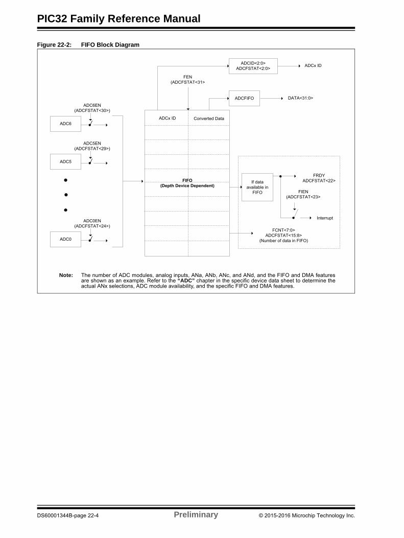
• FIFO and DMA engine for dedicated ADC modules (see Note 2)
• Early interrupt generation resulting in faster processing of converted data
• Designed for motor control, power conversion, and general purpose applications
The dedicated ADC modules use a single input (or its alternate) and is intended for high-speedand precise sampling of time-sensitive or transient inputs, whereas the shared ADC moduleincorporates a multiplexer on the input to facilitate a larger group of inputs, with slower sampling,and provides flexible automated scanning option through the input scan logic.
For each ADC module, the analog inputs are connected to the S&H capacitor. The clock,sampling time, and output data resolution for each ADC module can be set independently. TheADC module performs the conversion of the input analog signal based on the configurations setin the registers. When conversion is complete, the final result is stored in the result buffer for thespecific analog input and is passed to the digital filter and digital comparator if configured to usedata from this particular sample.
A simplified block diagram of the ADC module is illustrated in Figure 22-1.
Note: This family reference manual section is meant to serve as a complement to devicedata sheets. Depending on the device, this manual section may not apply to allPIC32 devices.
Please refer to the note at the beginning of the “ADC” chapter in the current devicedata sheet to check whether this document supports the device you are using.
Device data sheets and family reference manual sections are available fordownload from the Microchip Worldwide Web site at: http://www.microchip.com
Note 1: Depending on the device, the 12-bit High-Speed SAR ADC has up to seven dedicated ADC modules and one shared ADC module. Throughout this chapter, the diagrams and code examples refer to a device with seven dedicated ADC modules (ADC0-ADC6) and one shared ADC (ADC7). Please consult the “ADC” chapter in the specific device data sheet to determine which ADC modules are available for your device.
2: This feature is not available on all devices. Refer to the “ADC” chapter in the specific device data sheet to determine availability.
3: Prior to enabling the ADC module, the user application must copy the ADC calibration data (DEVADCx) from the Configuration memory into the ADC Configuration registers (ADC0CFG-ADC7CFG). Refer to the “ADC” chapter in the specific device data sheet for more information.
DS60001344B-page 22-2 Preliminary © 2015-2016 Microchip Technology Inc.

Section 22. 12-bit High-Speed SAR ADC
Figure 22-1: ADC Block Diagram
Note: The number of ADC modules, analog inputs, ANa, ANb, ANc, and ANd, and the FIFO and DMA featuresare shown as an example. Refer to the “ADC” chapter in the specific device data sheet to determine theactual ANx selections, ADC module availability, and the specific FIFO and DMA features.
ADC0
ADC7
AVDD AVSS VREF+ VREF-
VREFSEL<2:0>
VREFH VREFL
ADCSEL<1:0>
CONCLKDIV<5:0>
TCY FRC PBCLK
TQADCDIV<6:0>(ADCxTIME<22:16>)
ADCDIV<6:0>(ADCCON2<6:0>)
TAD0-TAD6
TAD7
ADDATA0
…...
ADDATA63
(Dedicated ADC)
(Dedicated ADC)
FIFO
DMA
Digital Filter
Digital ComparatorInterrupt/Event
Capacitive Voltage Divider (CVD)
Interrupt/Event
Triggers,Turbo Channel,
Scan Control Logic
Trigger
Status and Control Registers
ADC6
SH0ALT<1:0>(ADCTRGMODE<17:16>)
ANxVREFL
01
DIFFx<1>(ADCIMCONx<x>)
ANa
AN1VREFL
01
DIFF1<1>(ADCIMCON1<3>)
SH6ALT<1:0>(ADCTRGMODE<29:28>)
ANxVREFL
01
DIFFx<1>(ADCIMCONx<x>)
AN49
IVCTMU
IVBAT
AN48
AN7
CVD Capacitor
TCLK
ANbANcANd
00011011
ANbANcANd
00011011
SYSTEM
BUS
ANa
Interrupt
Data
© 2015-2016 Microchip Technology Inc. Preliminary DS60001344B-page 22-3
PIC32 Family Reference Manual
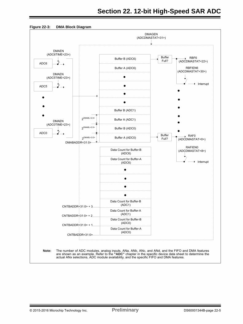
Figure 22-2: FIFO Block Diagram
FEN(ADCFSTAT<31>
FIFO(Depth Device Dependent)
ADCFIFO DATA<31:0>
ADCID<2:0>ADCFSTAT<2:0>
ADCx ID
ADCx ID Converted DataADC6
ADC6EN(ADCFSTAT<30>)
ADC5
ADC5EN(ADCFSTAT<29>)
ADC0
ADC0EN(ADCFSTAT<24>)
If data available in
FIFO
FRDYADCFSTAT<22>
FIEN(ADCFSTAT<23>
Interrupt
FCNT<7:0>ADCFSTAT<15:8>
(Number of data in FIFO)
Note: The number of ADC modules, analog inputs, ANa, ANb, ANc, and ANd, and the FIFO and DMA featuresare shown as an example. Refer to the “ADC” chapter in the specific device data sheet to determine theactual ANx selections, ADC module availability, and the specific FIFO and DMA features.
DS60001344B-page 22-4 Preliminary © 2015-2016 Microchip Technology Inc.
Section 22. 12-bit High-Speed SAR ADC
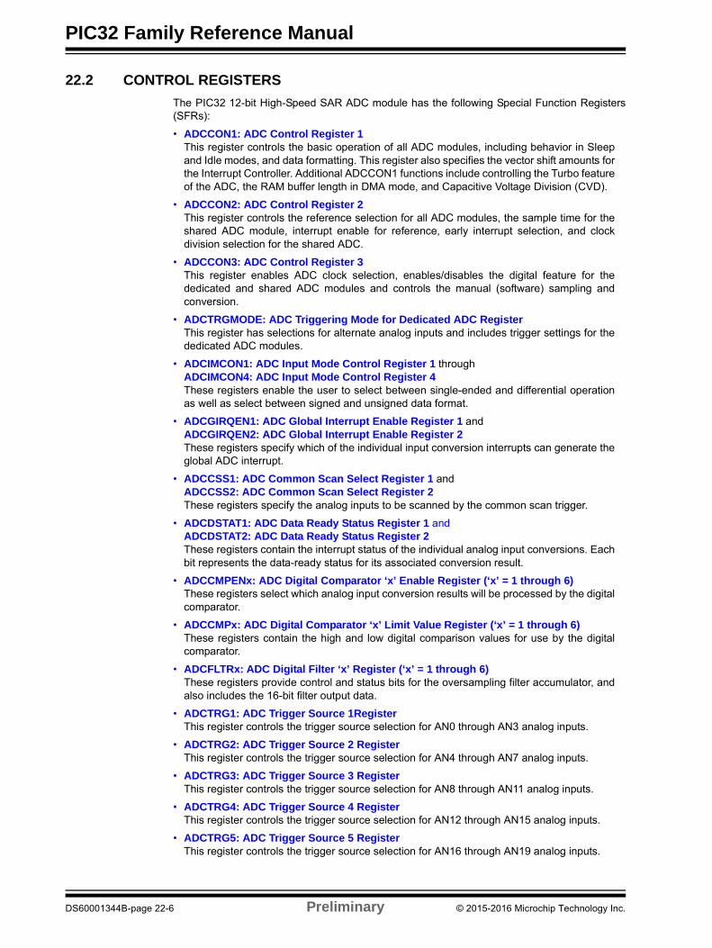
Figure 22-3: DMA Block Diagram
DMAGEN(ADCDMASTAT<31>)
ADC6
DMAEN(ADC6TIME<23>)
ADC5
ADC0
DMAEN(ADC5TIME<23>)
DMAEN(ADC0TIME<23>)
Buffer A (ADC0)
Buffer B (ADC0)
Buffer A (ADC1)
Buffer B (ADC1)
Buffer A (ADC6)
Buffer B (ADC6)
2DMABL<2:0>
2DMABL<2:0>
2DMABL<2:0>
BufferFull?
RAF0(ADCDMASTAT<0>)
RAFIEN0(ADCDMASTAT<8>)
Interrupt
BufferFull?
RBF6(ADCDMASTAT<22>)
RBFIEN6(ADCDMASTAT<30>)
Interrupt
Data Count for Buffer-A (ADC0)
Data Count for Buffer-B (ADC0)
Data Count for Buffer-A (ADC1)
Data Count for Buffer-B (ADC1)
Data Count for Buffer-A (ADC6)
Data Count for Buffer-B (ADC6)
DMABADDR<31:0>
CNTBADDR<31:0>
CNTBADDR<31:0> + 1
CNTBADDR<31:0> + 2
CNTBADDR<31:0> + 3
Note: The number of ADC modules, analog inputs, ANa, ANb, ANc, and ANd, and the FIFO and DMA featuresare shown as an example. Refer to the “ADC” chapter in the specific device data sheet to determine theactual ANx selections, ADC module availability, and the specific FIFO and DMA features.
© 2015-2016 Microchip Technology Inc. Preliminary DS60001344B-page 22-5
PIC32 Family Reference Manual
22.2 CONTROL REGISTERS
The PIC32 12-bit High-Speed SAR ADC module has the following Special Function Registers(SFRs):
• ADCCON1: ADC Control Register 1This register controls the basic operation of all ADC modules, including behavior in Sleepand Idle modes, and data formatting. This register also specifies the vector shift amounts forthe Interrupt Controller. Additional ADCCON1 functions include controlling the Turbo featureof the ADC, the RAM buffer length in DMA mode, and Capacitive Voltage Division (CVD).
• ADCCON2: ADC Control Register 2This register controls the reference selection for all ADC modules, the sample time for theshared ADC module, interrupt enable for reference, early interrupt selection, and clockdivision selection for the shared ADC.
• ADCCON3: ADC Control Register 3This register enables ADC clock selection, enables/disables the digital feature for thededicated and shared ADC modules and controls the manual (software) sampling andconversion.
• ADCTRGMODE: ADC Triggering Mode for Dedicated ADC RegisterThis register has selections for alternate analog inputs and includes trigger settings for thededicated ADC modules.
• ADCIMCON1: ADC Input Mode Control Register 1 through ADCIMCON4: ADC Input Mode Control Register 4These registers enable the user to select between single-ended and differential operationas well as select between signed and unsigned data format.
• ADCGIRQEN1: ADC Global Interrupt Enable Register 1 andADCGIRQEN2: ADC Global Interrupt Enable Register 2These registers specify which of the individual input conversion interrupts can generate theglobal ADC interrupt.
• ADCCSS1: ADC Common Scan Select Register 1 andADCCSS2: ADC Common Scan Select Register 2These registers specify the analog inputs to be scanned by the common scan trigger.
• ADCDSTAT1: ADC Data Ready Status Register 1 and ADCDSTAT2: ADC Data Ready Status Register 2These registers contain the interrupt status of the individual analog input conversions. Eachbit represents the data-ready status for its associated conversion result.
• ADCCMPENx: ADC Digital Comparator ‘x’ Enable Register (‘x’ = 1 through 6)These registers select which analog input conversion results will be processed by the digitalcomparator.
• ADCCMPx: ADC Digital Comparator ‘x’ Limit Value Register (‘x’ = 1 through 6)These registers contain the high and low digital comparison values for use by the digitalcomparator.
• ADCFLTRx: ADC Digital Filter ‘x’ Register (‘x’ = 1 through 6)These registers provide control and status bits for the oversampling filter accumulator, andalso includes the 16-bit filter output data.
• ADCTRG1: ADC Trigger Source 1RegisterThis register controls the trigger source selection for AN0 through AN3 analog inputs.
• ADCTRG2: ADC Trigger Source 2 RegisterThis register controls the trigger source selection for AN4 through AN7 analog inputs.
• ADCTRG3: ADC Trigger Source 3 RegisterThis register controls the trigger source selection for AN8 through AN11 analog inputs.
• ADCTRG4: ADC Trigger Source 4 RegisterThis register controls the trigger source selection for AN12 through AN15 analog inputs.
• ADCTRG5: ADC Trigger Source 5 RegisterThis register controls the trigger source selection for AN16 through AN19 analog inputs.
DS60001344B-page 22-6 Preliminary © 2015-2016 Microchip Technology Inc.

Section 22. 12-bit High-Speed SAR ADC
• ADCTRG6: ADC Trigger Source 6 RegisterThis register controls the trigger source selection for AN20 through AN23 analog inputs.
• ADCTRG7: ADC Trigger Source 7 RegisterThis register controls the trigger source selection for AN24 through AN27 analog inputs.
• ADCTRG8: ADC Trigger Source 8 RegisterThis register controls the trigger source selection for AN28 through AN31 analog inputs.
• ADCCMPCON1: ADC Digital Comparator 1 Control RegisterThis register controls the operation of Digital Comparator 1, including the generation of inter-rupts, comparison criteria to be used, and provides status when a comparator event occurs.Additionally, this register provides the output data of CVD.
• ADCCMPCONx: ADC Digital Comparator ‘x’ Control Register (‘x’ = 2 through 6)These registers control the operation of Digital Comparators 2 through 6, including thegeneration of interrupts and the comparison criteria to be used. This register also providesstatus when a comparator event occurs.
• ADCFSTAT: ADC FIFO Status RegisterThis register specifies the status of the dedicated ADC module FIFO.
• ADCFIFO: ADC FIFO Data RegisterThis register specifies the output value of the dedicated ADC module FIFO.
• ADCBASE: ADC Base RegisterThese registers specify the base address of the user ADC Interrupt Service Routine (ISR)jump table.
• ADCDMASTAT: ADC DMA Status RegisterThis register contains the DMA status bits.
• ADCCNTB: ADC Sample Count Base Address RegisterThis register contains the base address of the sample count in RAM. In addition to storyingthe converted data of each dedicated ADC module in RAM, DMA also stores the convertedsample count.
• ADCDMAB: ADC DMA Base Address RegisterThis register contains the base address of RAM for the DMA engine.
• ADCTRGSNS: ADC Trigger Level/Edge Sensitivity RegisterThis register contains the setting for trigger level for each ADC analog input.
• ADCxTIME: Dedicated ADCx Timing Register ‘x’ (‘x’ = 0 through 6)These registers contains the time and clock setting for dedicated analog input.
• ADCEIEN1: ADC Early Interrupt Enable Register 1 andADCEIEN2: ADC Early Interrupt Enable Register 2These registers contains bits to enable or disable early interrupt for individual analog inputs.
• ADCEISTAT1: ADC Early Interrupt Status Register 1 and ADCEISTAT2: ADC Early Interrupt Status Register 2These registers contain status bits for early interrupt for individual analog inputs.
• ADCANCON: ADC Analog Warm-up Control Register
This register contains the warm-up control settings for the analog and bias circuit of the ADCmodule.
• ADCDATAx: ADC Output Data Register (‘x’ = 0 through 63)
These registers are the analog-to-digital conversion output data registers. The ADCDATAxregister is associated with each analog input, 0-63.
• ADCxCFG: ADCx Configuration Register ‘x’ (‘x’ = 0 through 7)
These registers specify the ADC module configuration data.
• ADCSYSCFG0: ADC System Configuration Register 0 and ADCSYSCFG1: ADC System Configuration Register 1
These registers contain read-only bits corresponding to the analog input.
© 2015-2016 Microchip Technology Inc. Preliminary DS60001344B-page 22-7

PIC
32 Fam
ily Referen
ce Ma
nu
al
DS
60
00
13
44
B-p
ag
e 2
2-8
Prelim
inary
© 2
01
5-2
01
6 M
icroch
ip T
ech
no
log
y Inc.
ding registers appear after the summaries, which Refer to the “ADC” chapter in the specific device
5 Bit 20/4 Bit 19/3 Bit 18/2 Bit 17/1 Bit 16/0
STRGSRC<4:0>
:0> STRGLVL DMABL<2:0>
C<9:0>
ADCDIV<6:0>
5 DIGEN4 DIGEN3 DIGEN2 DIGEN1 DIGEN0
ADINSEL<5:0>
2ALT<1:0> SH1ALT<1:0> SH0ALT<1:0>
N5 SSAMPEN4 SSAMPEN3 SSAMPEN2 SSAMPEN1 SSAMPEN0
SIGN10 DIFF9 SIGN9 DIFF8 SIGN8
SIGN2 DIFF1 SIGN1 DIFF0 SIGN0
SIGN26 DIFF25 SIGN25 DIFF24 SIGN24
SIGN18 DIFF17 SIGN17 DIFF16 SIGN16
SIGN42 DIFF41 SIGN41 DIFF40 SIGN40
SIGN34 DIFF33 SIGN33 DIFF32 SIGN32
SIGN58 DIFF57 SIGN57 DIFF56 SIGN56
SIGN50 DIFF49 SIGN49 DIFF48 SIGN48
1 AGIEN20 AGIEN19 AGIEN18 AGIEN17 AGIEN16
5 AGIEN4 AGIEN3 AGIEN2 AGIEN1 AGIEN0
3 AGIEN52 AGIEN51 AGIEN50 AGIEN49 AGIEN48
7 AGIEN36 AGIEN35 AGIEN34 AGIEN33 AGIEN32
CSS20 CSS19 CSS18 CSS17 CSS16
CSS4 CSS3 CSS2 CSS1 CSS0
CSS52 CSS51 CSS50 CSS49 CSS48
CSS36 CSS35 CSS34 CSS33 CSS32
1 ARDY20 ARDY19 ARDY18 ARDY17 ARDY16
ARDY4 ARDY3 ARDY2 ARDY1 ARDY0
3 ARDY52 ARDY51 ARDY50 ARDY49 ARDY48
7 ARDY36 ARDY35 ARDY34 ARDY33 ARDY32
1 CMPE20 CMPE19 CMPE18 CMPE17 CMPE16
5 CMPE4 CMPE3 CMPE2 CMPE1 CMPE0
CHNLID<4:0>
TRGSRC2<4:0>
TRGSRC0<4:0>
TRGSRC6<4:0>
TRGSRC4<4:0>
TRGSRC10<4:0>
TRGSRC8<4:0>
TRGSRC14<4:0>
TRGSRC12<4:0>
TRGSRC18<4:0>
TRGSRC16<4:0>
VADCx Flash registers into the corresponding ADCxCFG
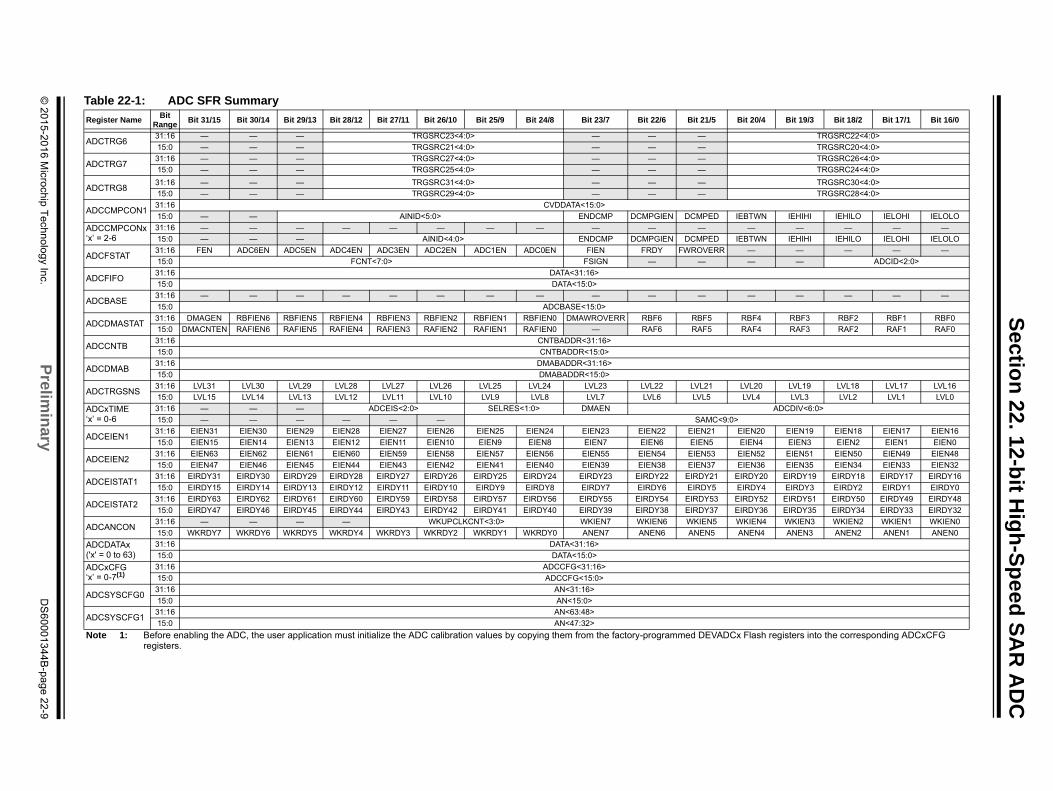
Table 22-1 provides a summary of all ADC Special Function Registers (SFRs). Corresponinclude a detailed description of each bit. Depending on the device, functionality will vary.data sheet to determine which registers are available for your device.
Table 22-1: ADC SFR Summary
Register NameBit
RangeBit 31/15 Bit 30/14 Bit 29/13 Bit 28/12 Bit 27/11 Bit 26/10 Bit 25/9 Bit 24/8 Bit 23/7 Bit 22/6 Bit 21/
ADCCON131:16 TRBEN TRBERR TRBMST<2:0> TRBSLV<2:0> FRACT SELRES<1:0>
15:0 ON — SIDL AICPMPEN CVDEN FSSCLKEN FSPBCLKEN — — IRQVS<2
ADCCON231:16 BGVRRDY REFFLT EOSRDY CVDCPL<2:0> SAM
15:0 BGVRIEN REFFLTIEN EOSIEN ADCEIOVR ECRIEN ADCEIS<2:0> —
ADCCON331:16 ADCSEL<1:0> CONCLKDIV<5:0> DIGEN7 DIGEN6 DIGEN
15:0 VREFSEL<2:0> TRGSUSP UPDIEN UPDRDY SAMP RQCNVRT GLSWTRG GSWTRG
ADCTRGMODE31:16 — — SH6ALT<1:0> SH5ALT<1:0> SH4ALT<1:0> SH3ALT<1:0> SH
15:0 — STRGEN6 STRGEN5 STRGEN4 STRGEN3 STRGEN2 STRGEN1 STRGEN0 — SSAMPEN6 SSAMPE
ADCIMCON131:16 DIFF15 SIGN15 DIFF14 SIGN14 DIFF13 SIGN13 DIFF12 SIGN12 DIFF11 SIGN11 DIFF10
15:0 DIFF7 SIGN7 DIFF6 SIGN6 DIFF5 SIGN5 DIFF4 SIGN4 DIFF3 SIGN3 DIFF2
ADCIMCON231:16 DIFF31 SIGN31 DIFF30 SIGN30 DIFF29 SIGN29 DIFF28 SIGN28 DIFF27 SIGN27 DIFF26
15:0 DIFF23 SIGN23 DIFF22 SIGN22 DIFF21 SIGN21 DIFF20 SIGN20 DIFF19 SIGN19 DIFF18
ADCIMCON331:16 DIFF47 SIGN47 DIFF46 SIGN46 DIFF45 SIGN45 DIFF44 SIGN44 DIFF43 SIGN43 DIFF42
15:0 DIFF39 SIGN39 DIFF38 SIGN38 DIFF37 SIGN37 DIFF36 SIGN36 DIFF35 SIGN35 DIFF34
ADCIMCON431:16 DIFF63 SIGN63 DIFF62 SIGN62 DIFF61 SIGN61 DIFF60 SIGN60 DIFF59 SIGN59 DIFF58
15:0 DIFF55 SIGN55 DIFF54 SIGN54 DIFF53 SIGN53 DIFF52 SIGN52 DIFF51 SIGN51 DIFF50
ADCGIRQEN131:16 AGIEN31 AGIEN30 AGIEN29 AGIEN28 AGIEN27 AGIEN26 AGIEN25 AGIEN24 AGIEN23 AGIEN22 AGIEN2
15:0 AGIEN15 AGIEN14 AGIEN13 AGIEN12 AGIEN11 AGIEN10 AGIEN9 AGIEN8 AGIEN7 AGIEN6 AGIEN
ADCGIRQEN231:16 AGIEN63 AGIEN62 AGIEN61 AGIEN60 AGIEN59 AGIEN58 AGIEN57 AGIEN56 AGIEN55 AGIEN54 AGIEN5
15:0 AGIEN47 AGIEN46 AGIEN45 AGIEN44 AGIEN43 AGIEN42 AGIEN41 AGIEN40 AGIEN39 AGIEN38 AGIEN3
ADCCSS131:16 CSS31 CSS30 CSS29 CSS28 CSS27 CSS26 CSS25 CSS24 CSS23 CSS22 CSS21
15:0 CSS15 CSS14 CSS13 CSS12 CSS11 CSS10 CSS9 CSS8 CSS7 CSS6 CSS5
ADCCSS231:16 CSS63 CSS62 CSS61 CSS60 CSS59 CSS58 CSS57 CSS56 CSS55 CSS54 CSS53
15:0 CSS47 CSS46 CSS45 CSS44 CSS43 CSS42 CSS41 CSS40 CSS39 CSS38 CSS37
ADCDSTAT131:16 ARDY31 ARDY30 ARDY29 ARDY28 ARDY27 ARDY26 ARDY25 ARDY24 ARDY23 ARDY22 ARDY2
15:0 ARDY15 ARDY14 ARDY13 ARDY12 ARDY11 ARDY10 ARDY9 ARDY8 ARDY7 ARDY6 ARDY5
ADCDSTAT231:16 ARDY63 ARDY62 ARDY61 ARDY60 ARDY59 ARDY58 ARDY57 ARDY56 ARDY55 ARDY54 ARDY5
15:0 ARDY47 ARDY46 ARDY45 ARDY44 ARDY43 ARDY42 ARDY41 ARDY40 ARDY39 ARDY38 ARDY3
ADCCMPENx‘x’ = 1-6
31:16 CMPE31 CMPE30 CMPE29 CMPE28 CMPE27 CMPE26 CMPE25 CMPE24 CMPE23 CMPE22 CMPE2
15:0 CMPE15 CMPE14 CMPE13 CMPE12 CMPE11 CMPE10 CMPE9 CMPE8 CMPE7 CMPE6 CMPE
ADCCMPx‘x’ = 1-6
31:16 DCMPHI<15:0>
15:0 DCMPLO<15:0>
ADCFLTRx‘x’ = 1-6
31:16 AFEN DATA16EN DFMODE OVRSAM<2:0> AFGIEN AFRDY — — —
15:0 FLTRDATA<15:0>
ADCTRG131:16 — — — TRGSRC3<4:0> — — —
15:0 — — — TRGSRC1<4:0> — — —
ADCTRG231:16 — — — TRGSRC7<4:0> — — —
15:0 — — — TRGSRC5<4:0> — — —
ADCTRG331:16 — — — TRGSRC11<4:0> — — —
15:0 — — — TRGSRC9<4:0> — — —
ADCTRG431:16 — — — TRGSRC15<4:0> — — —
15:0 — — — TRGSRC13<4:0> — — —
ADCTRG531:16 — — — TRGSRC19<4:0> — — —
15:0 — — — TRGSRC17<4:0> — — —
Note 1: Before enabling the ADC, the user application must initialize the ADC calibration values by copying them from the factory-programmed DEregisters.
© 2
01
5-2
01
6 M
icroch
ip T
ech
no
log
y Inc.
Prelim
inary
DS
60
00
13
44
B-p
ag
e 2
2-9
Sectio
n 22
. 12-bit H
igh
-Sp
eed S
AR
AD
C
TRGSRC22<4:0>
TRGSRC20<4:0>
TRGSRC26<4:0>
TRGSRC24<4:0>
TRGSRC30<4:0>
TRGSRC28<4:0>
IEBTWN IEHIHI IEHILO IELOHI IELOLO
— — — — —
IEBTWN IEHIHI IEHILO IELOHI IELOLO
— — — — —
— — ADCID<2:0>
— — — — —
RBF4 RBF3 RBF2 RBF1 RBF0
RAF4 RAF3 RAF2 RAF1 RAF0
LVL20 LVL19 LVL18 LVL17 LVL16
LVL4 LVL3 LVL2 LVL1 LVL0
ADCDIV<6:0>
>
EIEN20 EIEN19 EIEN18 EIEN17 EIEN16
EIEN4 EIEN3 EIEN2 EIEN1 EIEN0
EIEN52 EIEN51 EIEN50 EIEN49 EIEN48
EIEN36 EIEN35 EIEN34 EIEN33 EIEN32
EIRDY20 EIRDY19 EIRDY18 EIRDY17 EIRDY16
EIRDY4 EIRDY3 EIRDY2 EIRDY1 EIRDY0
EIRDY52 EIRDY51 EIRDY50 EIRDY49 EIRDY48
EIRDY36 EIRDY35 EIRDY34 EIRDY33 EIRDY32
WKIEN4 WKIEN3 WKIEN2 WKIEN1 WKIEN0
ANEN4 ANEN3 ANEN2 ANEN1 ANEN0
T
Bit 20/4 Bit 19/3 Bit 18/2 Bit 17/1 Bit 16/0
x Flash registers into the corresponding ADCxCFG
ADCTRG631:16 — — — TRGSRC23<4:0> — — —
15:0 — — — TRGSRC21<4:0> — — —
ADCTRG731:16 — — — TRGSRC27<4:0> — — —
15:0 — — — TRGSRC25<4:0> — — —
ADCTRG831:16 — — — TRGSRC31<4:0> — — —
15:0 — — — TRGSRC29<4:0> — — —
ADCCMPCON131:16 CVDDATA<15:0>
15:0 — — AINID<5:0> ENDCMP DCMPGIEN DCMPED
ADCCMPCONx‘x’ = 2-6
31:16 — — — — — — — — — — —
15:0 — — — AINID<4:0> ENDCMP DCMPGIEN DCMPED
ADCFSTAT31:16 FEN ADC6EN ADC5EN ADC4EN ADC3EN ADC2EN ADC1EN ADC0EN FIEN FRDY FWROVERR
15:0 FCNT<7:0> FSIGN — —
ADCFIFO31:16 DATA<31:16>
15:0 DATA<15:0>
ADCBASE31:16 — — — — — — — — — — —
15:0 ADCBASE<15:0>
ADCDMASTAT31:16 DMAGEN RBFIEN6 RBFIEN5 RBFIEN4 RBFIEN3 RBFIEN2 RBFIEN1 RBFIEN0 DMAWROVERR RBF6 RBF5
15:0 DMACNTEN RAFIEN6 RAFIEN5 RAFIEN4 RAFIEN3 RAFIEN2 RAFIEN1 RAFIEN0 — RAF6 RAF5
ADCCNTB31:16 CNTBADDR<31:16>
15:0 CNTBADDR<15:0>
ADCDMAB31:16 DMABADDR<31:16>
15:0 DMABADDR<15:0>
ADCTRGSNS31:16 LVL31 LVL30 LVL29 LVL28 LVL27 LVL26 LVL25 LVL24 LVL23 LVL22 LVL21
15:0 LVL15 LVL14 LVL13 LVL12 LVL11 LVL10 LVL9 LVL8 LVL7 LVL6 LVL5
ADCxTIME‘x’ = 0-6
31:16 — — — ADCEIS<2:0> SELRES<1:0> DMAEN
15:0 — — — — — — SAMC<9:0
ADCEIEN131:16 EIEN31 EIEN30 EIEN29 EIEN28 EIEN27 EIEN26 EIEN25 EIEN24 EIEN23 EIEN22 EIEN21
15:0 EIEN15 EIEN14 EIEN13 EIEN12 EIEN11 EIEN10 EIEN9 EIEN8 EIEN7 EIEN6 EIEN5
ADCEIEN231:16 EIEN63 EIEN62 EIEN61 EIEN60 EIEN59 EIEN58 EIEN57 EIEN56 EIEN55 EIEN54 EIEN53
15:0 EIEN47 EIEN46 EIEN45 EIEN44 EIEN43 EIEN42 EIEN41 EIEN40 EIEN39 EIEN38 EIEN37
ADCEISTAT131:16 EIRDY31 EIRDY30 EIRDY29 EIRDY28 EIRDY27 EIRDY26 EIRDY25 EIRDY24 EIRDY23 EIRDY22 EIRDY21
15:0 EIRDY15 EIRDY14 EIRDY13 EIRDY12 EIRDY11 EIRDY10 EIRDY9 EIRDY8 EIRDY7 EIRDY6 EIRDY5
ADCEISTAT231:16 EIRDY63 EIRDY62 EIRDY61 EIRDY60 EIRDY59 EIRDY58 EIRDY57 EIRDY56 EIRDY55 EIRDY54 EIRDY53
15:0 EIRDY47 EIRDY46 EIRDY45 EIRDY44 EIRDY43 EIRDY42 EIRDY41 EIRDY40 EIRDY39 EIRDY38 EIRDY37
ADCANCON31:16 — — — — WKUPCLKCNT<3:0> WKIEN7 WKIEN6 WKIEN5
15:0 WKRDY7 WKRDY6 WKRDY5 WKRDY4 WKRDY3 WKRDY2 WKRDY1 WKRDY0 ANEN7 ANEN6 ANEN5
ADCDATAx('x' = 0 to 63)
31:16 DATA<31:16>
15:0 DATA<15:0>
ADCxCFG‘x’ = 0-7(1)
31:16 ADCCFG<31:16>
15:0 ADCCFG<15:0>
ADCSYSCFG031:16 AN<31:16>
15:0 AN<15:0>
ADCSYSCFG131:16 AN<63:48>
15:0 AN<47:32>
able 22-1: ADC SFR Summary
Register NameBit
RangeBit 31/15 Bit 30/14 Bit 29/13 Bit 28/12 Bit 27/11 Bit 26/10 Bit 25/9 Bit 24/8 Bit 23/7 Bit 22/6 Bit 21/5
Note 1: Before enabling the ADC, the user application must initialize the ADC calibration values by copying them from the factory-programmed DEVADCregisters.
PIC32 Family Reference Manual
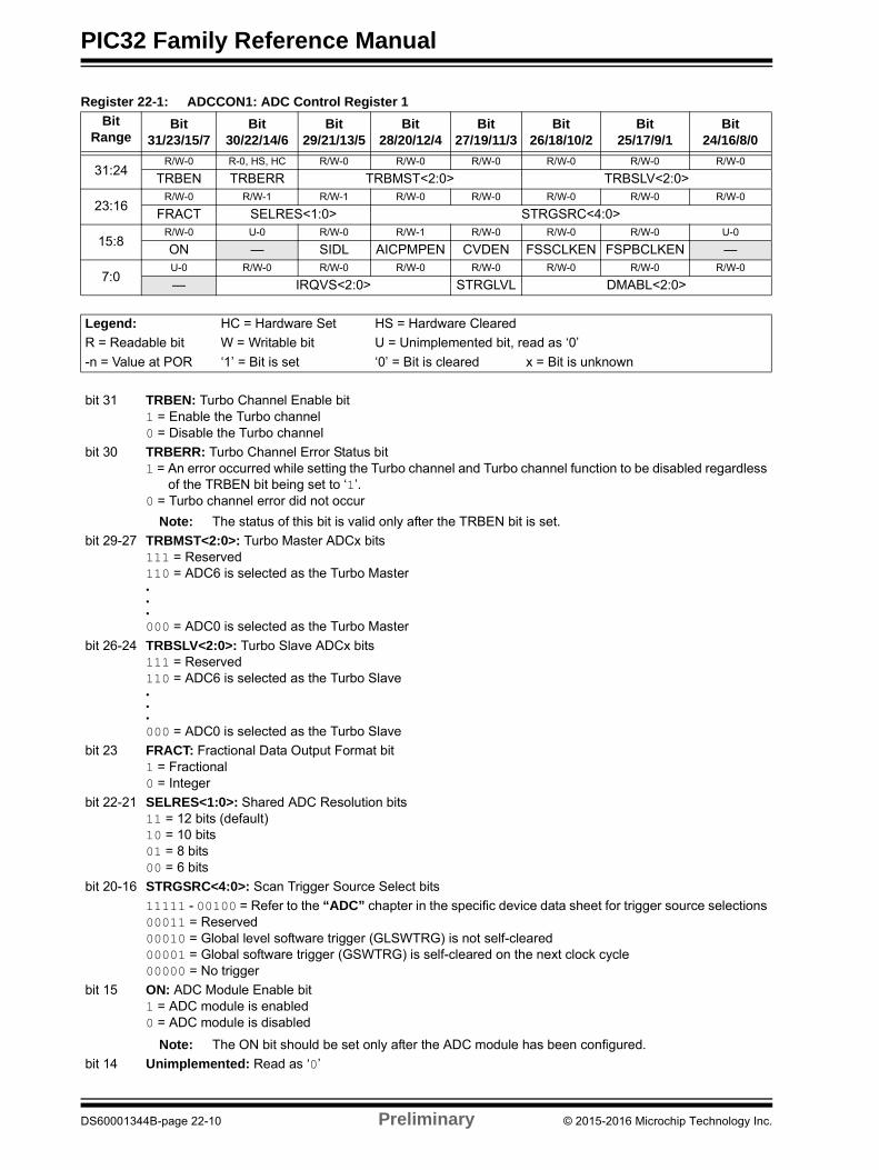
Register 22-1: ADCCON1: ADC Control Register 1
Bit Range
Bit31/23/15/7
Bit30/22/14/6
Bit29/21/13/5
Bit28/20/12/4
Bit27/19/11/3
Bit26/18/10/2
Bit25/17/9/1
Bit24/16/8/0
31:24R/W-0 R-0, HS, HC R/W-0 R/W-0 R/W-0 R/W-0 R/W-0 R/W-0
TRBEN TRBERR TRBMST<2:0> TRBSLV<2:0>
23:16R/W-0 R/W-1 R/W-1 R/W-0 R/W-0 R/W-0 R/W-0 R/W-0
FRACT SELRES<1:0> STRGSRC<4:0>
15:8R/W-0 U-0 R/W-0 R/W-1 R/W-0 R/W-0 R/W-0 U-0
ON — SIDL AICPMPEN CVDEN FSSCLKEN FSPBCLKEN —
7:0U-0 R/W-0 R/W-0 R/W-0 R/W-0 R/W-0 R/W-0 R/W-0
— IRQVS<2:0> STRGLVL DMABL<2:0>
Legend: HC = Hardware Set HS = Hardware Cleared
R = Readable bit W = Writable bit U = Unimplemented bit, read as ‘0’
-n = Value at POR ‘1’ = Bit is set ‘0’ = Bit is cleared x = Bit is unknown
bit 31 TRBEN: Turbo Channel Enable bit1 = Enable the Turbo channel0 = Disable the Turbo channel
bit 30 TRBERR: Turbo Channel Error Status bit1 = An error occurred while setting the Turbo channel and Turbo channel function to be disabled regardless
of the TRBEN bit being set to ‘1’.0 = Turbo channel error did not occur
Note: The status of this bit is valid only after the TRBEN bit is set.
bit 29-27 TRBMST<2:0>: Turbo Master ADCx bits111 = Reserved110 = ADC6 is selected as the Turbo Master•••000 = ADC0 is selected as the Turbo Master
bit 26-24 TRBSLV<2:0>: Turbo Slave ADCx bits111 = Reserved110 = ADC6 is selected as the Turbo Slave•••000 = ADC0 is selected as the Turbo Slave
bit 23 FRACT: Fractional Data Output Format bit1 = Fractional0 = Integer
bit 22-21 SELRES<1:0>: Shared ADC Resolution bits11 = 12 bits (default)10 = 10 bits01 = 8 bits00 = 6 bits
bit 20-16 STRGSRC<4:0>: Scan Trigger Source Select bits
11111 - 00100 = Refer to the “ADC” chapter in the specific device data sheet for trigger source selections00011 = Reserved00010 = Global level software trigger (GLSWTRG) is not self-cleared00001 = Global software trigger (GSWTRG) is self-cleared on the next clock cycle00000 = No trigger
bit 15 ON: ADC Module Enable bit1 = ADC module is enabled0 = ADC module is disabled
Note: The ON bit should be set only after the ADC module has been configured.
bit 14 Unimplemented: Read as ‘0’
DS60001344B-page 22-10 Preliminary © 2015-2016 Microchip Technology Inc.

Section 22. 12-bit High-Speed SAR ADC
bit 13 SIDL: Stop in Idle Mode bit
1 = Discontinue module operation when the device enters Idle mode0 = Continue module operation in Idle mode
bit 12 AICPMPEN: Analog Input Charge Pump Enable bit
1 = Analog input charge pump is enabled (default)0 = Analog input charge pump is disabled
bit 11 CVDEN: Capacitive Voltage Division Enable bit
1 = CVD operation is enabled0 = CVD operation is disabled
bit 10 FSSCLKEN: Fast Synchronous System Clock to ADC Control Clock bit
1 = Fast synchronous system clock to ADC control clock is enabled0 = Fast synchronous system clock to ADC control clock is disabled
bit 9 FSPBCLKEN: Fast Synchronous Peripheral Clock to ADC Control Clock bit
1 = Fast synchronous peripheral clock to ADC control clock is enabled0 = Fast synchronous peripheral clock to ADC control clock is disabled
bit 8-7 Unimplemented: Read as ‘0’
bit 6-4 IRQVS<2:0>: Interrupt Vector Shift bits
To determine interrupt vector address, this bit specifies the amount of left shift done to the ARDYx statusbits in the ADCDSTAT1 and ADCDSTAT2 registers, prior to adding with the ADCBASE register (see22.6.2 “ADC Base Register (ADCBASE) Usage” for more information).
Interrupt Vector Address = Read Value of ADCBASE = Value written to ADCBASE + x << IRQVS<2:0>,where ‘x’ is the smallest active input ID from the ADCDSTAT1 or ADCDSTAT2 registers (which has highestpriority).
111 = Shift x left 7 bit position110 = Shift x left 6 bit position101 = Shift x left 5 bit position100 = Shift x left 4 bit position011 = Shift x left 3 bit position010 = Shift x left 2 bit position001 = Shift x left 1 bit position000 = Shift x left 0 bit position
bit 3 STRGLVL: Scan Trigger High Level/Positive Edge Sensitivity bit
1 = Scan trigger is high level sensitive. Once STRIG mode is selected (TRGSRCx<4:0> in the ADCTRGxregister), the scan trigger will continue for all selected analog inputs, until the STRIG option is removed.
0 = Scan trigger is positive edge sensitive. Once STRIG mode is selected (TRGSRCx<4:0> in theADCTRGx register), only a single scan trigger will be generated, which will complete the scan of allselected analog inputs.
bit 2-0 DMABL<2:0>: DMA Buffer Length Size bits
111 = Allocates 128 locations in RAM to each analog input110 = Allocates 64 locations in RAM to each analog input101 = Allocates 32 locations in RAM to each analog input100 = Allocates 16 locations in RAM to each analog input011 = Allocates 8 locations in RAM to each analog input010 = Allocates 4 locations in RAM to each analog input001 = Allocates 2 locations in RAM to each analog input000 = Allocates 1 location in RAM to each analog input
Note: Since each output data is 16-bit wide, one location consists of 2 bytes.
Register 22-1: ADCCON1: ADC Control Register 1 (Continued)
© 2015-2016 Microchip Technology Inc. Preliminary DS60001344B-page 22-11

PIC32 Family Reference Manual
Register 22-2: ADCCON2: ADC Control Register 2
Bit Range Bit31/23/15/7
Bit30/22/14/6
Bit29/21/13/5
Bit28/20/12/4
Bit27/19/11/3
Bit26/18/10/2
Bit25/17/9/1
Bit24/16/8/0
31:24R-0, HS, HC R-0, HS, HC R-0, HS, HC R/W-0 R/W-0 R/W-0 R/W-0 R/W-0
BGVRRDY REFFLT EOSRDY CVDCPL<2:0> SAMC<9:9>
23:16R/W-0 R/W-0 R/W-0 R/W-0 R/W-0 R/W-0 R/W-0 R/W-0
SAMC<7:0>
15:8R/W-0 R/W-0 R/W-0 R/W-0 R/W-0 R/W-0 R/W-0 R/W-0
BGVRIEN REFFLTIEN EOSIEN ADCEIOVR ECRIEN ADCEIS<2:0>
7:0U-0 R/W-0 R/W-0 R/W-0 R/W-0 R/W-0 R/W-0 R/W-0
— ADCDIV<6:0>
Legend: HC = Hardware Set HS = Hardware Cleared r = Reserved
R = Readable bit W = Writable bit U = Unimplemented bit, read as ‘0’
-n = Value at POR ‘1’ = Bit is set ‘0’ = Bit is cleared x = Bit is unknown
bit 31 BGVRRDY: Band Gap Voltage/ADC Reference Voltage Status bit
1 = Both band gap voltage and ADC reference voltages (VREF) are ready0 = Either or both band gap voltage and ADC reference voltages (VREF) are not ready
Data processing is valid only after the BGVRRDY bit is set by hardware, so the application code mustcheck that the BGVRRDY bit is set to ensure data validity. This bit is set to ‘0’ when the ON bit(ADCCON1<15>) = 0.
bit 30 REFFLT: Band Gap/VREF/AVDD BOR Fault Status bit
1 = Fault in band gap or the VREF voltage while the ON bit (ADCCON1<15>) was set. Most likely a bandgap or VREF fault will be caused by a BOR of the analog VDD supply.
0 = Band gap and VREF voltage are working properly
This bit is cleared when the ON bit (ADCCON1<15>) = 0 and the BGVRRDY bit = 1.
bit 29 EOSRDY: End of Scan Interrupt Status bit
1 = All analog inputs are considered for scanning through the scan trigger (all analog inputs specified inthe ADCCSS1 and ADCCSS2 registers) have completed scanning
0 = Scanning has not completed
This bit is cleared when ADCCON2<31:24> are read in software.
bit 28-26 CVDCPL<2:0>: Capacitor Voltage Divider (CVD) Setting bit
111 = 7 * 2.5 pF = 17.5 pF110 = 6 * 2.5 pF = 15 pF101 = 5 * 2.5 pF = 12.5 pF100 = 4 * 2.5 pF = 10 pF011 = 3 * 2.5 pF = 7.5 pF010 = 2 * 2.5 pF = 5 pF001 = 1 * 2.5 pF = 2.5 pF000 = 0 * 2.5 pF = 0 pF
bit 25-16 SAMC<9:0>: Sample Time for the Shared ADC bits
1111111111 = 1025 TAD
•••
0000000001 = 3 TAD
0000000000 = 2 TAD
Where TAD = period of the ADC conversion clock for the Shared ADC controlled by the ADCDIV<6:0> bits.
bit 15 BGVRIEN: Band Gap/VREF Voltage Ready Interrupt Enable bit
1 = Interrupt will be generated when the BGVRRDY bit is set0 = No interrupt is generated when the BGVRRDY bit is set
DS60001344B-page 22-12 Preliminary © 2015-2016 Microchip Technology Inc.
Section 22. 12-bit High-Speed SAR ADC
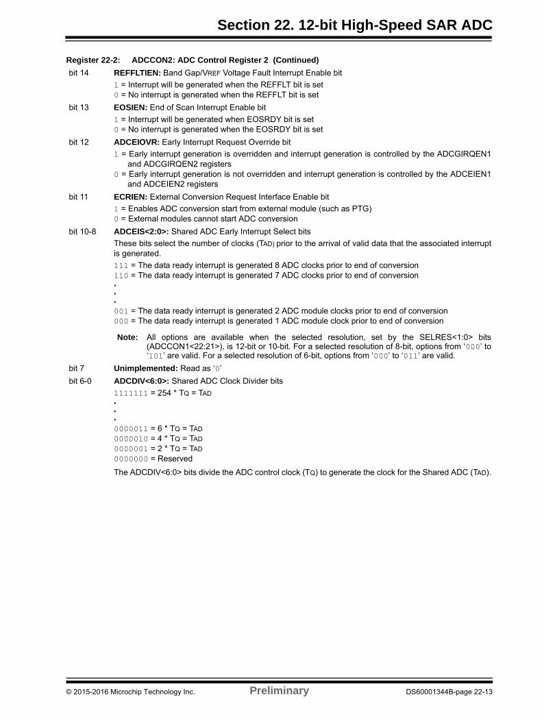
bit 14 REFFLTIEN: Band Gap/VREF Voltage Fault Interrupt Enable bit
1 = Interrupt will be generated when the REFFLT bit is set0 = No interrupt is generated when the REFFLT bit is set
bit 13 EOSIEN: End of Scan Interrupt Enable bit
1 = Interrupt will be generated when EOSRDY bit is set0 = No interrupt is generated when the EOSRDY bit is set
bit 12 ADCEIOVR: Early Interrupt Request Override bit
1 = Early interrupt generation is overridden and interrupt generation is controlled by the ADCGIRQEN1and ADCGIRQEN2 registers
0 = Early interrupt generation is not overridden and interrupt generation is controlled by the ADCEIEN1and ADCEIEN2 registers
bit 11 ECRIEN: External Conversion Request Interface Enable bit
1 = Enables ADC conversion start from external module (such as PTG)0 = External modules cannot start ADC conversion
bit 10-8 ADCEIS<2:0>: Shared ADC Early Interrupt Select bits
These bits select the number of clocks (TAD) prior to the arrival of valid data that the associated interruptis generated.
111 = The data ready interrupt is generated 8 ADC clocks prior to end of conversion110 = The data ready interrupt is generated 7 ADC clocks prior to end of conversion•••
001 = The data ready interrupt is generated 2 ADC module clocks prior to end of conversion000 = The data ready interrupt is generated 1 ADC module clock prior to end of conversion
Note: All options are available when the selected resolution, set by the SELRES<1:0> bits(ADCCON1<22:21>), is 12-bit or 10-bit. For a selected resolution of 8-bit, options from ‘000’ to‘101’ are valid. For a selected resolution of 6-bit, options from ‘000’ to ‘011’ are valid.
bit 7 Unimplemented: Read as ‘0’
bit 6-0 ADCDIV<6:0>: Shared ADC Clock Divider bits
1111111 = 254 * TQ = TAD
•••
0000011 = 6 * TQ = TAD
0000010 = 4 * TQ = TAD
0000001 = 2 * TQ = TAD
0000000 = Reserved
The ADCDIV<6:0> bits divide the ADC control clock (TQ) to generate the clock for the Shared ADC (TAD).
Register 22-2: ADCCON2: ADC Control Register 2 (Continued)
© 2015-2016 Microchip Technology Inc. Preliminary DS60001344B-page 22-13

PIC32 Family Reference Manual
Register 22-3: ADCCON3: ADC Control Register 3
Bit Range
Bit31/23/15/7
Bit30/22/14/6
Bit29/21/13/5
Bit28/20/12/4
Bit27/19/11/3
Bit26/18/10/2
Bit25/17/9/1
Bit24/16/8/0
31:24R/W-0 R/W-0 R/W-0 R/W-0 R/W-0 R/W-0 R/W-0 R/W-0
ADCSEL<1:0> CONCLKDIV<5:0>
23:16R/W-0 R/W-0 R/W-0 R/W-0 R/W-0 R/W-0 R/W-0 R/W-0
DIGEN7(5) DIGEN6(5) DIGEN5(5) DIGEN4(5) DIGEN3(5) DIGEN2(5) DIGEN1(5) DIGEN0(5)
15:8R/W-0 R/W-0 R/W-0 R/W-0 R/W-0 R-0, HS, HC R/W-0 R-0, HS, HC
VREFSEL<2:0> TRGSUSP UPDIEN UPDRDY SAMP(1,2,3,4) RQCNVRT
7:0R/W-0 R-0, HS, HC R/W-0 R/W-0 R/W-0 R/W-0 R/W-0 R/W-0
GLSWTRG GSWTRG ADINSEL<5:0>(5)
Legend: HC = Hardware Set HS = Hardware Cleared
R = Readable bit W = Writable bit U = Unimplemented bit, read as ‘0’
-n = Value at POR ‘1’ = Bit is set ‘0’ = Bit is cleared x = Bit is unknown
bit 31-30 ADCSEL<1:0>: Analog-to-Digital Clock Source (TCLK) bits
11 = System Clock (TCY)10 = REFCLK301 = FRC Oscillator output00 = Peripheral bus clock (PBCLK)
bit 29-24 CONCLKDIV<5:0>: Analog-to-Digital Control Clock (TQ) Divider bits
111111 = 126 * TCLK = TQ
•••
000011 = 6 * TCLK = TQ
000010 = 4 * TCLK = TQ
000001 = 2 * TCLK = TQ
000000 = TCLK = TQ
bit 23 DIGEN7: ADC7 Digital Enable bit(5)
1 = ADC7 is digital enabled0 = ADC7 is digital disabled
bit 22 DIGEN6: ADC6 Digital Enable bit(5)
1 = ADC6 is digital enabled0 = ADC6 is digital disabled
bit 21 DIGEN5: ADC5 Digital Enable bit(5)
1 = ADC5 is digital enabled0 = ADC5 is digital disabled
Note 1: The SAMP bit has the highest priority and setting this bit will keep the S&H circuit in Sample mode until the bit is cleared. Also, usage of the SAMP bit will cause settings of the SAMC<9:0> bits (ADCCON2<25:16>) to be ignored.
2: The SAMP bit only connects Class 2 and Class 3 analog inputs to the shared ADC. All Class 1 analog inputs are not affected by the SAMP bit.
3: The SAMP bit is not a self-clearing bit and it is the responsibility of application software to first clear this bit and only after setting the RQCNVRT bit to start the analog-to-digital conversion.
4: Normally, when the SAMP and RQCNVRT bits are used by software routines, all TRGSRCx<4:0> bits and STRGSRC<4:0> bits should be set to ‘00000’ to disable all external hardware triggers and prevent them from interfering with the software-controlled sampling command signal SAMP and with the software-controlled trigger RQCNVRT.
5: Depending on the device, the function will vary. Refer to the “ADC” chapter in the specific device data sheet to determine the function that is available for your device.
DS60001344B-page 22-14 Preliminary © 2015-2016 Microchip Technology Inc.

Section 22. 12-bit High-Speed SAR ADC
bit 20 DIGEN4: ADC4 Digital Enable bit(5)
1 = ADC4 is digital enabled0 = ADC4 is digital disabled
bit 19 DIGEN3: ADC3 Digital Enable bit(5)
1 = ADC3 is digital enabled0 = ADC3 is digital disabled
bit 18 DIGEN2: ADC2 Digital Enable bit(5)
1 = ADC2 is digital enabled0 = ADC2 is digital disabled
bit 17 DIGEN1: ADC1 Digital Enable bit(5)
1 = ADC1 is digital enabled0 = ADC1 is digital disabled
bit 16 DIGEN0: ADC0 Digital Enable bit(5)
1 = ADC0 is digital enabled0 = ADC0 is digital disabled
bit 15-13 VREFSEL<2:0>: Voltage Reference (VREF) Input Selection bits
bit 12 TRGSUSP: Trigger Suspend bit1 = Triggers are blocked from starting a new analog-to-digital conversion, but the ADC module is not disabled0 = Triggers are not blocked
bit 11 UPDIEN: Update Ready Interrupt Enable bit1 = Interrupt will be generated when the UPDRDY bit is set by hardware0 = No interrupt is generated
bit 10 UPDRDY: ADC Update Ready Status bit1 = ADC SFRs can be updated0 = ADC SFRs cannot be updated
Note: This bit is only active while the TRGSUSP bit is set and there are no more running conversions ofany ADC modules.
bit 9 SAMP: Class 2 and Class 3 Analog Input Sampling Enable bit(1,2,3,4)
1 = The ADC S&H amplifier is sampling0 = The ADC S&H amplifier is holding
Register 22-3: ADCCON3: ADC Control Register 3 (Continued)
Note 1: The SAMP bit has the highest priority and setting this bit will keep the S&H circuit in Sample mode until the bit is cleared. Also, usage of the SAMP bit will cause settings of the SAMC<9:0> bits (ADCCON2<25:16>) to be ignored.
2: The SAMP bit only connects Class 2 and Class 3 analog inputs to the shared ADC. All Class 1 analog inputs are not affected by the SAMP bit.
3: The SAMP bit is not a self-clearing bit and it is the responsibility of application software to first clear this bit and only after setting the RQCNVRT bit to start the analog-to-digital conversion.
4: Normally, when the SAMP and RQCNVRT bits are used by software routines, all TRGSRCx<4:0> bits and STRGSRC<4:0> bits should be set to ‘00000’ to disable all external hardware triggers and prevent them from interfering with the software-controlled sampling command signal SAMP and with the software-controlled trigger RQCNVRT.
5: Depending on the device, the function will vary. Refer to the “ADC” chapter in the specific device data sheet to determine the function that is available for your device.
VREFSEL<2:0> ADREF+ ADREF-
111 AVDD Internal VREFL
110 Internal VREFH AVSS
101 Internal VREFH External VREFL
100 Internal VREFH Internal VREFL
011 External VREFH External VREFL
010 AVDD External VREFL
001 External VREFH AVss000 AVDD AVss
© 2015-2016 Microchip Technology Inc. Preliminary DS60001344B-page 22-15
PIC32 Family Reference Manual
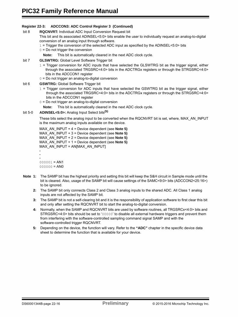
bit 8 RQCNVRT: Individual ADC Input Conversion Request bitThis bit and its associated ADINSEL<5:0> bits enable the user to individually request an analog-to-digital conversion of an analog input through software.1 = Trigger the conversion of the selected ADC input as specified by the ADINSEL<5:0> bits0 = Do not trigger the conversion
Note: This bit is automatically cleared in the next ADC clock cycle.
bit 7 GLSWTRG: Global Level Software Trigger bit1 = Trigger conversion for ADC inputs that have selected the GLSWTRG bit as the trigger signal, either
through the associated TRGSRC<4:0> bits in the ADCTRGx registers or through the STRGSRC<4:0>bits in the ADCCON1 register
0 = Do not trigger an analog-to-digital conversion
bit 6 GSWTRG: Global Software Trigger bit1 = Trigger conversion for ADC inputs that have selected the GSWTRG bit as the trigger signal, either
through the associated TRGSRC<4:0> bits in the ADCTRGx registers or through the STRGSRC<4:0>bits in the ADCCON1 register
0 = Do not trigger an analog-to-digital conversion
Note: This bit is automatically cleared in the next ADC clock cycle.
bit 5-0 ADINSEL<5:0>: Analog Input Select bits(5)
These bits select the analog input to be converted when the RQCNVRT bit is set, where, MAX_AN_INPUTis the maximum analog inputs available on the device.
MAX_AN_INPUT + 4 = Device dependent (see Note 5)MAX_AN_INPUT + 3 = Device dependent (see Note 5)MAX_AN_INPUT + 2 = Device dependent (see Note 5)MAX_AN_INPUT + 1 = Device dependent (see Note 5)MAX_AN_INPUT = AN[MAX_AN_INPUT]•••
000001 = AN1000000 = AN0
Register 22-3: ADCCON3: ADC Control Register 3 (Continued)
Note 1: The SAMP bit has the highest priority and setting this bit will keep the S&H circuit in Sample mode until the bit is cleared. Also, usage of the SAMP bit will cause settings of the SAMC<9:0> bits (ADCCON2<25:16>) to be ignored.
2: The SAMP bit only connects Class 2 and Class 3 analog inputs to the shared ADC. All Class 1 analog inputs are not affected by the SAMP bit.
3: The SAMP bit is not a self-clearing bit and it is the responsibility of application software to first clear this bit and only after setting the RQCNVRT bit to start the analog-to-digital conversion.
4: Normally, when the SAMP and RQCNVRT bits are used by software routines, all TRGSRCx<4:0> bits and STRGSRC<4:0> bits should be set to ‘00000’ to disable all external hardware triggers and prevent them from interfering with the software-controlled sampling command signal SAMP and with the software-controlled trigger RQCNVRT.
5: Depending on the device, the function will vary. Refer to the “ADC” chapter in the specific device data sheet to determine the function that is available for your device.
DS60001344B-page 22-16 Preliminary © 2015-2016 Microchip Technology Inc.
Section 22. 12-bit High-Speed SAR ADC
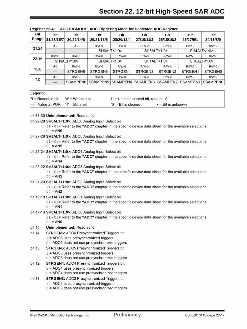
Register 22-4: ADCTRGMODE: ADC Triggering Mode for Dedicated ADC RegisterBit
RangeBit
31/23/15/7Bit
30/22/14/6Bit
29/21/13/5Bit
28/20/12/4Bit
27/19/11/3Bit
26/18/10/2Bit
25/17/9/1Bit
24/16/8/0
31:24U-0 U-0 R/W-0 R/W-0 R/W-0 R/W-0 R/W-0 R/W-0
— — SH6ALT<1:0> SH5ALT<1:0> SH4ALT<1:0>
23:16R/W-0 R/W-0 R/W-0 R/W-0 R/W-0 R/W-0 R/W-0 R/W-0
SH3ALT<1:0> SH2ALT<1:0> SH1ALT<1:0> SH0ALT<1:0>
15:8U-0 R/W-0 R/W-0 R/W-0 R/W-0 R/W-0 R/W-0 R/W-0
— STRGEN6 STRGEN5 STRGEN4 STRGEN3 STRGEN2 STRGEN1 STRGEN0
7:0U-0 R/W-0 R/W-0 R/W-0 R/W-0 R/W-0 R/W-0 R/W-0
— SSAMPEN6 SSAMPEN5 SSAMPEN4 SSAMPEN3 SSAMPEN2 SSAMPEN1 SSAMPEN0
Legend:
R = Readable bit W = Writable bit U = Unimplemented bit, read as ‘0’
-n = Value at POR ‘1’ = Bit is set ‘0’ = Bit is cleared x = Bit is unknown
bit 31-30 Unimplemented: Read as ‘0’
bit 29-28 SH6ALT<1:0>: ADC6 Analog Input Select bit11 - 01= Refer to the “ADC” chapter in the specific device data sheet for the available selections00 = AN6
bit 27-26 SH5ALT<1:0>: ADC5 Analog Input Select bit11 - 01= Refer to the “ADC” chapter in the specific device data sheet for the available selections00 = AN5
bit 25-24 SH4ALT<1:0>: ADC4 Analog Input Select bit11 - 01= Refer to the “ADC” chapter in the specific device data sheet for the available selections00 = AN4
bit 23-22 SH3ALT<1:0>: ADC3 Analog Input Select bit11 - 01= Refer to the “ADC” chapter in the specific device data sheet for the available selections00 = AN3
bit 21-20 SH2ALT<1:0>: ADC2 Analog Input Select bit11 - 01= Refer to the “ADC” chapter in the specific device data sheet for the available selections00 = AN2
bit 19-18 SH1ALT<1:0>: ADC1 Analog Input Select bit11 - 01= Refer to the “ADC” chapter in the specific device data sheet for the available selections00 = AN1
bit 17-16 SH0ALT<1:0>: ADC0 Analog Input Select bit11 - 01= Refer to the “ADC” chapter in the specific device data sheet for the available selections00 = AN0
bit 15 Unimplemented: Read as ‘0’
bit 14 STRGEN6: ADC6 Presynchronized Triggers bit1 = ADC6 uses presynchronized triggers0 = ADC6 does not use presynchronized triggers
bit 13 STRGEN5: ADC5 Presynchronized Triggers bit1 = ADC5 uses presynchronized triggers0 = ADC5 does not use presynchronized triggers
bit 12 STRGEN4: ADC4 Presynchronized Triggers bit1 = ADC4 uses presynchronized triggers0 = ADC4 does not use presynchronized triggers
bit 11 STRGEN3: ADC3 Presynchronized Triggers bit1 = ADC3 uses presynchronized triggers0 = ADC3 does not use presynchronized triggers
© 2015-2016 Microchip Technology Inc. Preliminary DS60001344B-page 22-17
PIC32 Family Reference Manual
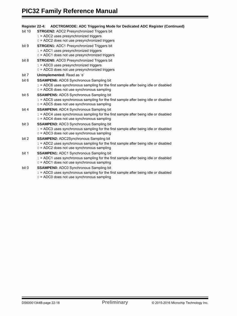
bit 10 STRGEN2: ADC2 Presynchronized Triggers bit1 = ADC2 uses presynchronized triggers0 = ADC2 does not use presynchronized triggers
bit 9 STRGEN1: ADC1 Presynchronized Triggers bit1 = ADC1 uses presynchronized triggers0 = ADC1 does not use presynchronized triggers
bit 8 STRGEN0: ADC0 Presynchronized Triggers bit1 = ADC0 uses presynchronized triggers0 = ADC0 does not use presynchronized triggers
bit 7 Unimplemented: Read as ‘0’
bit 6 SSAMPEN6: ADC6 Synchronous Sampling bit1 = ADC6 uses synchronous sampling for the first sample after being idle or disabled0 = ADC6 does not use synchronous sampling
bit 5 SSAMPEN5: ADC5 Synchronous Sampling bit1 = ADC5 uses synchronous sampling for the first sample after being idle or disabled0 = ADC5 does not use synchronous sampling
bit 4 SSAMPEN4: ADC4 Synchronous Sampling bit1 = ADC4 uses synchronous sampling for the first sample after being idle or disabled0 = ADC4 does not use synchronous sampling
bit 3 SSAMPEN3: ADC3 Synchronous Sampling bit1 = ADC3 uses synchronous sampling for the first sample after being idle or disabled0 = ADC3 does not use synchronous sampling
bit 2 SSAMPEN2: ADC2Synchronous Sampling bit1 = ADC2 uses synchronous sampling for the first sample after being idle or disabled0 = ADC2 does not use synchronous sampling
bit 1 SSAMPEN1: ADC1 Synchronous Sampling bit1 = ADC1 uses synchronous sampling for the first sample after being idle or disabled0 = ADC1 does not use synchronous sampling
bit 0 SSAMPEN0: ADC0 Synchronous Sampling bit1 = ADC0 uses synchronous sampling for the first sample after being idle or disabled0 = ADC0 does not use synchronous sampling
Register 22-4: ADCTRGMODE: ADC Triggering Mode for Dedicated ADC Register (Continued)
DS60001344B-page 22-18 Preliminary © 2015-2016 Microchip Technology Inc.

Section 22. 12-bit High-Speed SAR ADC
Register 22-5: ADCIMCON1: ADC Input Mode Control Register 1
Bit Range Bit31/23/15/7
Bit30/22/14/6
Bit29/21/13/5
Bit28/20/12/4
Bit27/19/11/3
Bit26/18/10/2
Bit25/17/9/1
Bit24/16/8/0
31:24R/W-0 R/W-0 R/W-0 R/W-0 R/W-0 R/W-0 R/W-0 R/W-0
DIFF15 SIGN15 DIFF14 SIGN14 DIFF13 SIGN13 DIFF12 SIGN12
23:16R/W-0 R/W-0 R/W-0 R/W-0 R/W-0 R/W-0 R/W-0 R/W-0
DIFF11 SIGN11 DIFF10 SIGN10 DIFF9 SIGN9 DIFF8 SIGN8
15:8R/W-0 R/W-0 R/W-0 R/W-0 R/W-0 R/W-0 R/W-0 R/W-0
DIFF7 SIGN7 DIFF6 SIGN6 DIFF5 SIGN5 DIFF4 SIGN4
7:0R/W-0 R/W-0 R/W-0 R/W-0 R/W-0 R/W-0 R/W-0 R/W-0
DIFF3 SIGN3 DIFF2 SIGN2 DIFF1 SIGN1 DIFF0 SIGN0
Legend:
R = Readable bit W = Writable bit U = Unimplemented bit, read as ‘0’
-n = Value at POR ‘1’ = Bit is set ‘0’ = Bit is cleared x = Bit is unknown
bit 31 DIFF15: AN15 Mode bit
1 = AN15 is using Differential mode
0 = AN15 is using Single-ended mode
bit 30 SIGN:15 AN15 Signed Data Mode bit
1 = AN15 is using Signed Data mode
0 = AN15 is using Unsigned Data mode
bit 29 DIFF14: AN14 Mode bit
1 = AN14 is using Differential mode
0 = AN14 is using Single-ended mode
bit 28 SIGN14: AN14 Signed Data Mode bit
1 = AN14 is using Signed Data mode
0 = AN14 is using Unsigned Data mode
bit 27 DIFF13: AN13 Mode bit
1 = AN13 is using Differential mode
0 = AN13 is using Single-ended mode
bit 26 SIGN13: AN13 Signed Data Mode bit
1 = AN13 is using Signed Data mode
0 = AN13 is using Unsigned Data mode
bit 25 DIFF12: AN12 Mode bit
1 = AN12 is using Differential mode
0 = AN12 is using Single-ended mode
bit 24 SIGN12: AN12 Signed Data Mode bit
1 = AN12 is using Signed Data mode
0 = AN12 is using Unsigned Data mode
bit 23 DIFF11: AN11 Mode bit
1 = AN11 is using Differential mode
0 = AN11 is using Single-ended mode
bit 22 SIGN11: AN11 Signed Data Mode bit
1 = AN11 is using Signed Data mode
0 = AN11 is using Unsigned Data mode
bit 21 DIFF10: AN10 Mode bit
1 = AN10 is using Differential mode
0 = AN10 is using Single-ended mode
© 2015-2016 Microchip Technology Inc. Preliminary DS60001344B-page 22-19
PIC32 Family Reference Manual
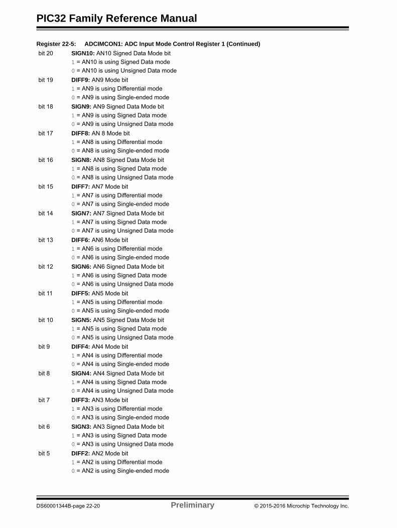
bit 20 SIGN10: AN10 Signed Data Mode bit
1 = AN10 is using Signed Data mode
0 = AN10 is using Unsigned Data mode
bit 19 DIFF9: AN9 Mode bit
1 = AN9 is using Differential mode
0 = AN9 is using Single-ended mode
bit 18 SIGN9: AN9 Signed Data Mode bit
1 = AN9 is using Signed Data mode
0 = AN9 is using Unsigned Data mode
bit 17 DIFF8: AN 8 Mode bit
1 = AN8 is using Differential mode
0 = AN8 is using Single-ended mode
bit 16 SIGN8: AN8 Signed Data Mode bit
1 = AN8 is using Signed Data mode
0 = AN8 is using Unsigned Data mode
bit 15 DIFF7: AN7 Mode bit
1 = AN7 is using Differential mode
0 = AN7 is using Single-ended mode
bit 14 SIGN7: AN7 Signed Data Mode bit
1 = AN7 is using Signed Data mode
0 = AN7 is using Unsigned Data mode
bit 13 DIFF6: AN6 Mode bit
1 = AN6 is using Differential mode
0 = AN6 is using Single-ended mode
bit 12 SIGN6: AN6 Signed Data Mode bit
1 = AN6 is using Signed Data mode
0 = AN6 is using Unsigned Data mode
bit 11 DIFF5: AN5 Mode bit
1 = AN5 is using Differential mode
0 = AN5 is using Single-ended mode
bit 10 SIGN5: AN5 Signed Data Mode bit
1 = AN5 is using Signed Data mode
0 = AN5 is using Unsigned Data mode
bit 9 DIFF4: AN4 Mode bit
1 = AN4 is using Differential mode
0 = AN4 is using Single-ended mode
bit 8 SIGN4: AN4 Signed Data Mode bit
1 = AN4 is using Signed Data mode
0 = AN4 is using Unsigned Data mode
bit 7 DIFF3: AN3 Mode bit
1 = AN3 is using Differential mode
0 = AN3 is using Single-ended mode
bit 6 SIGN3: AN3 Signed Data Mode bit
1 = AN3 is using Signed Data mode
0 = AN3 is using Unsigned Data mode
bit 5 DIFF2: AN2 Mode bit
1 = AN2 is using Differential mode
0 = AN2 is using Single-ended mode
Register 22-5: ADCIMCON1: ADC Input Mode Control Register 1 (Continued)
DS60001344B-page 22-20 Preliminary © 2015-2016 Microchip Technology Inc.
Section 22. 12-bit High-Speed SAR ADC
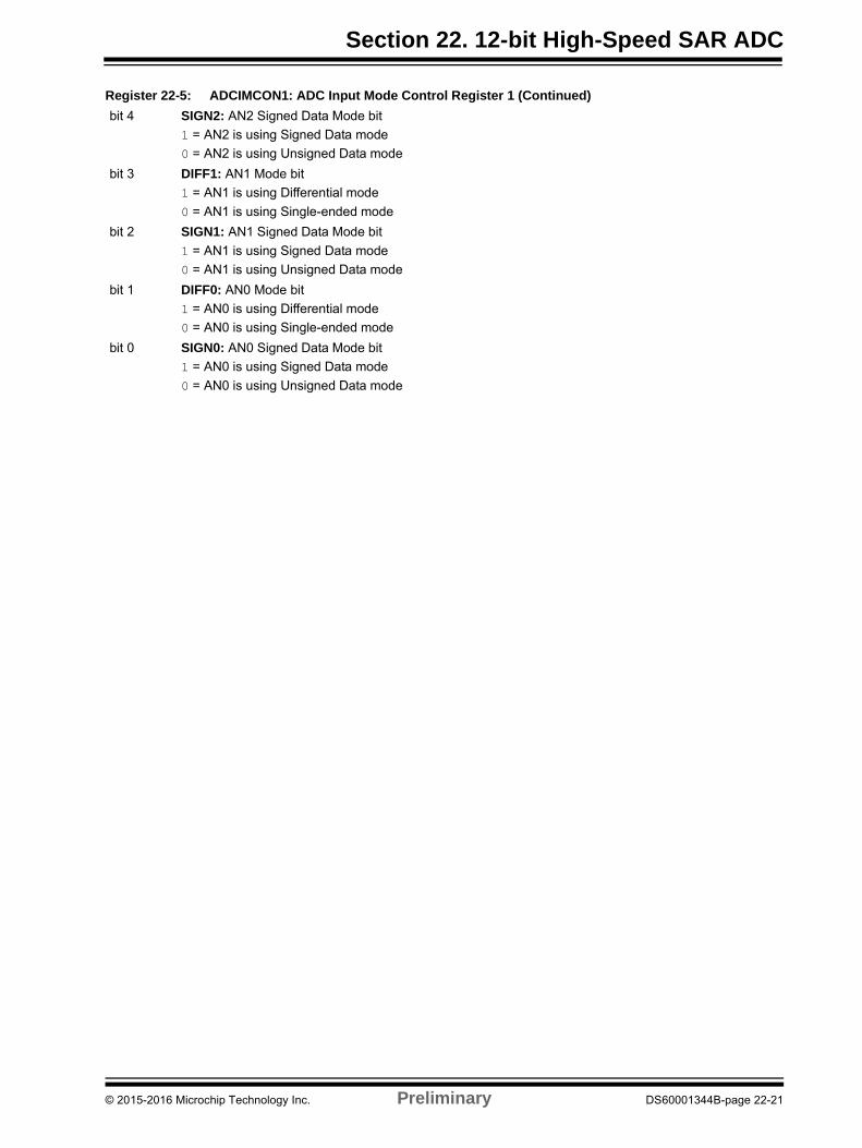
bit 4 SIGN2: AN2 Signed Data Mode bit
1 = AN2 is using Signed Data mode
0 = AN2 is using Unsigned Data mode
bit 3 DIFF1: AN1 Mode bit
1 = AN1 is using Differential mode
0 = AN1 is using Single-ended mode
bit 2 SIGN1: AN1 Signed Data Mode bit
1 = AN1 is using Signed Data mode
0 = AN1 is using Unsigned Data mode
bit 1 DIFF0: AN0 Mode bit
1 = AN0 is using Differential mode
0 = AN0 is using Single-ended mode
bit 0 SIGN0: AN0 Signed Data Mode bit
1 = AN0 is using Signed Data mode
0 = AN0 is using Unsigned Data mode
Register 22-5: ADCIMCON1: ADC Input Mode Control Register 1 (Continued)
© 2015-2016 Microchip Technology Inc. Preliminary DS60001344B-page 22-21
PIC32 Family Reference Manual
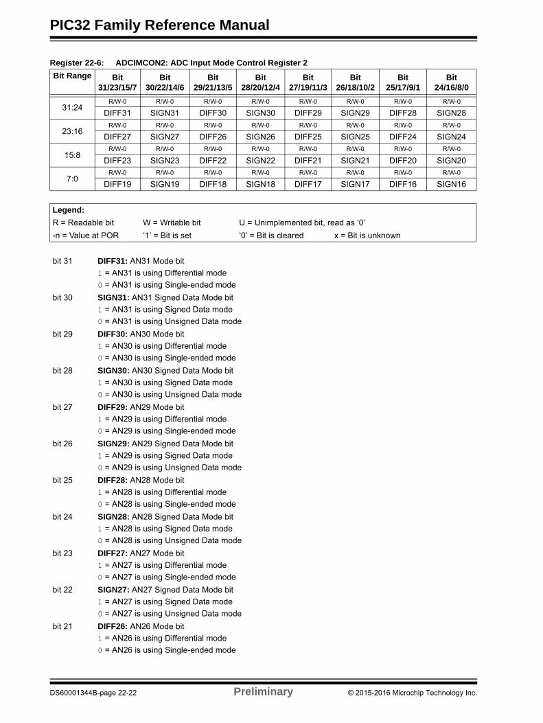
Register 22-6: ADCIMCON2: ADC Input Mode Control Register 2
Bit Range Bit31/23/15/7
Bit30/22/14/6
Bit29/21/13/5
Bit28/20/12/4
Bit27/19/11/3
Bit26/18/10/2
Bit25/17/9/1
Bit24/16/8/0
31:24R/W-0 R/W-0 R/W-0 R/W-0 R/W-0 R/W-0 R/W-0 R/W-0
DIFF31 SIGN31 DIFF30 SIGN30 DIFF29 SIGN29 DIFF28 SIGN28
23:16R/W-0 R/W-0 R/W-0 R/W-0 R/W-0 R/W-0 R/W-0 R/W-0
DIFF27 SIGN27 DIFF26 SIGN26 DIFF25 SIGN25 DIFF24 SIGN24
15:8R/W-0 R/W-0 R/W-0 R/W-0 R/W-0 R/W-0 R/W-0 R/W-0
DIFF23 SIGN23 DIFF22 SIGN22 DIFF21 SIGN21 DIFF20 SIGN20
7:0R/W-0 R/W-0 R/W-0 R/W-0 R/W-0 R/W-0 R/W-0 R/W-0
DIFF19 SIGN19 DIFF18 SIGN18 DIFF17 SIGN17 DIFF16 SIGN16
Legend:
R = Readable bit W = Writable bit U = Unimplemented bit, read as ‘0’
-n = Value at POR ‘1’ = Bit is set ‘0’ = Bit is cleared x = Bit is unknown
bit 31 DIFF31: AN31 Mode bit
1 = AN31 is using Differential mode
0 = AN31 is using Single-ended mode
bit 30 SIGN31: AN31 Signed Data Mode bit
1 = AN31 is using Signed Data mode
0 = AN31 is using Unsigned Data mode
bit 29 DIFF30: AN30 Mode bit
1 = AN30 is using Differential mode
0 = AN30 is using Single-ended mode
bit 28 SIGN30: AN30 Signed Data Mode bit
1 = AN30 is using Signed Data mode
0 = AN30 is using Unsigned Data mode
bit 27 DIFF29: AN29 Mode bit
1 = AN29 is using Differential mode
0 = AN29 is using Single-ended mode
bit 26 SIGN29: AN29 Signed Data Mode bit
1 = AN29 is using Signed Data mode
0 = AN29 is using Unsigned Data mode
bit 25 DIFF28: AN28 Mode bit
1 = AN28 is using Differential mode
0 = AN28 is using Single-ended mode
bit 24 SIGN28: AN28 Signed Data Mode bit
1 = AN28 is using Signed Data mode
0 = AN28 is using Unsigned Data mode
bit 23 DIFF27: AN27 Mode bit
1 = AN27 is using Differential mode
0 = AN27 is using Single-ended mode
bit 22 SIGN27: AN27 Signed Data Mode bit
1 = AN27 is using Signed Data mode
0 = AN27 is using Unsigned Data mode
bit 21 DIFF26: AN26 Mode bit
1 = AN26 is using Differential mode
0 = AN26 is using Single-ended mode
DS60001344B-page 22-22 Preliminary © 2015-2016 Microchip Technology Inc.
Section 22. 12-bit High-Speed SAR ADC
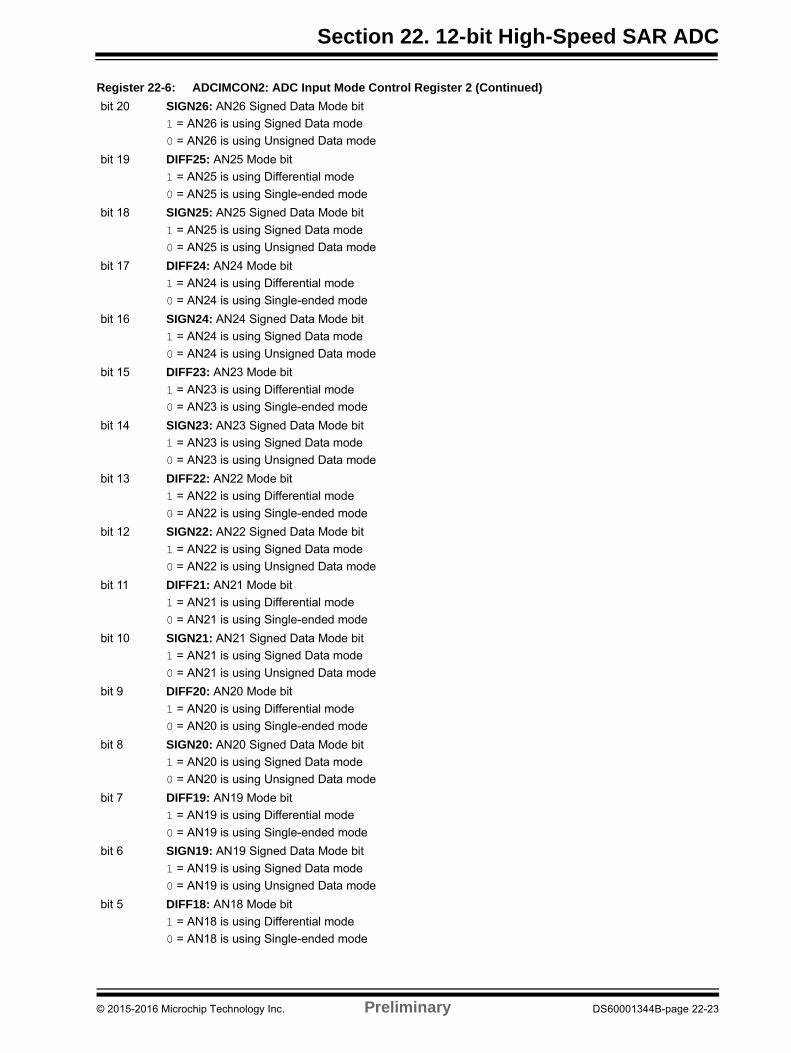
bit 20 SIGN26: AN26 Signed Data Mode bit
1 = AN26 is using Signed Data mode
0 = AN26 is using Unsigned Data mode
bit 19 DIFF25: AN25 Mode bit
1 = AN25 is using Differential mode
0 = AN25 is using Single-ended mode
bit 18 SIGN25: AN25 Signed Data Mode bit
1 = AN25 is using Signed Data mode
0 = AN25 is using Unsigned Data mode
bit 17 DIFF24: AN24 Mode bit
1 = AN24 is using Differential mode
0 = AN24 is using Single-ended mode
bit 16 SIGN24: AN24 Signed Data Mode bit
1 = AN24 is using Signed Data mode
0 = AN24 is using Unsigned Data mode
bit 15 DIFF23: AN23 Mode bit
1 = AN23 is using Differential mode
0 = AN23 is using Single-ended mode
bit 14 SIGN23: AN23 Signed Data Mode bit
1 = AN23 is using Signed Data mode
0 = AN23 is using Unsigned Data mode
bit 13 DIFF22: AN22 Mode bit
1 = AN22 is using Differential mode
0 = AN22 is using Single-ended mode
bit 12 SIGN22: AN22 Signed Data Mode bit
1 = AN22 is using Signed Data mode
0 = AN22 is using Unsigned Data mode
bit 11 DIFF21: AN21 Mode bit
1 = AN21 is using Differential mode
0 = AN21 is using Single-ended mode
bit 10 SIGN21: AN21 Signed Data Mode bit
1 = AN21 is using Signed Data mode
0 = AN21 is using Unsigned Data mode
bit 9 DIFF20: AN20 Mode bit
1 = AN20 is using Differential mode
0 = AN20 is using Single-ended mode
bit 8 SIGN20: AN20 Signed Data Mode bit
1 = AN20 is using Signed Data mode
0 = AN20 is using Unsigned Data mode
bit 7 DIFF19: AN19 Mode bit
1 = AN19 is using Differential mode
0 = AN19 is using Single-ended mode
bit 6 SIGN19: AN19 Signed Data Mode bit
1 = AN19 is using Signed Data mode
0 = AN19 is using Unsigned Data mode
bit 5 DIFF18: AN18 Mode bit
1 = AN18 is using Differential mode
0 = AN18 is using Single-ended mode
Register 22-6: ADCIMCON2: ADC Input Mode Control Register 2 (Continued)
© 2015-2016 Microchip Technology Inc. Preliminary DS60001344B-page 22-23
PIC32 Family Reference Manual
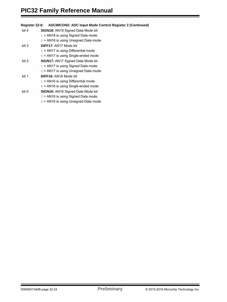
bit 4 SIGN18: AN18 Signed Data Mode bit
1 = AN18 is using Signed Data mode
0 = AN18 is using Unsigned Data mode
bit 3 DIFF17: AN17 Mode bit
1 = AN17 is using Differential mode
0 = AN17 is using Single-ended mode
bit 2 SIGN17: AN17 Signed Data Mode bit
1 = AN17 is using Signed Data mode
0 = AN17 is using Unsigned Data mode
bit 1 DIFF16: AN16 Mode bit
1 = AN16 is using Differential mode
0 = AN16 is using Single-ended mode
bit 0 SIGN16: AN16 Signed Data Mode bit
1 = AN16 is using Signed Data mode
0 = AN16 is using Unsigned Data mode
Register 22-6: ADCIMCON2: ADC Input Mode Control Register 2 (Continued)
DS60001344B-page 22-24 Preliminary © 2015-2016 Microchip Technology Inc.
Section 22. 12-bit High-Speed SAR ADC
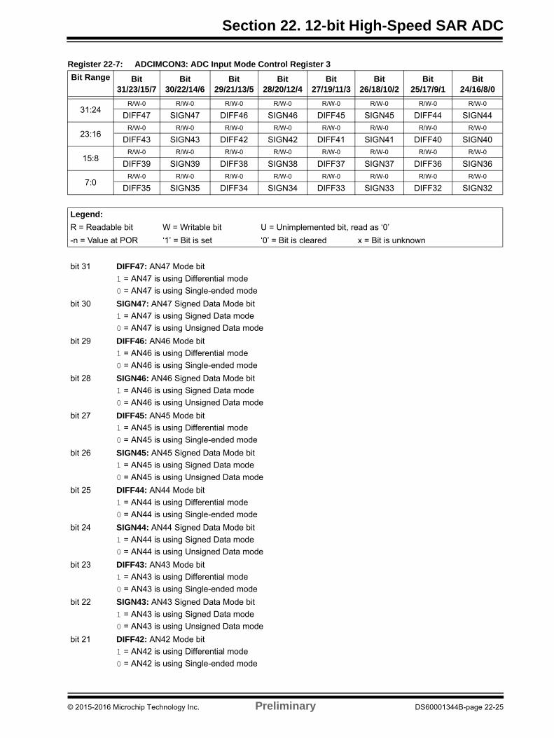
Register 22-7: ADCIMCON3: ADC Input Mode Control Register 3
Bit Range Bit31/23/15/7
Bit30/22/14/6
Bit29/21/13/5
Bit28/20/12/4
Bit27/19/11/3
Bit26/18/10/2
Bit25/17/9/1
Bit24/16/8/0
31:24R/W-0 R/W-0 R/W-0 R/W-0 R/W-0 R/W-0 R/W-0 R/W-0
DIFF47 SIGN47 DIFF46 SIGN46 DIFF45 SIGN45 DIFF44 SIGN44
23:16R/W-0 R/W-0 R/W-0 R/W-0 R/W-0 R/W-0 R/W-0 R/W-0
DIFF43 SIGN43 DIFF42 SIGN42 DIFF41 SIGN41 DIFF40 SIGN40
15:8R/W-0 R/W-0 R/W-0 R/W-0 R/W-0 R/W-0 R/W-0 R/W-0
DIFF39 SIGN39 DIFF38 SIGN38 DIFF37 SIGN37 DIFF36 SIGN36
7:0R/W-0 R/W-0 R/W-0 R/W-0 R/W-0 R/W-0 R/W-0 R/W-0
DIFF35 SIGN35 DIFF34 SIGN34 DIFF33 SIGN33 DIFF32 SIGN32
Legend:
R = Readable bit W = Writable bit U = Unimplemented bit, read as ‘0’
-n = Value at POR ‘1’ = Bit is set ‘0’ = Bit is cleared x = Bit is unknown
bit 31 DIFF47: AN47 Mode bit
1 = AN47 is using Differential mode
0 = AN47 is using Single-ended mode
bit 30 SIGN47: AN47 Signed Data Mode bit
1 = AN47 is using Signed Data mode
0 = AN47 is using Unsigned Data mode
bit 29 DIFF46: AN46 Mode bit
1 = AN46 is using Differential mode
0 = AN46 is using Single-ended mode
bit 28 SIGN46: AN46 Signed Data Mode bit
1 = AN46 is using Signed Data mode
0 = AN46 is using Unsigned Data mode
bit 27 DIFF45: AN45 Mode bit
1 = AN45 is using Differential mode
0 = AN45 is using Single-ended mode
bit 26 SIGN45: AN45 Signed Data Mode bit
1 = AN45 is using Signed Data mode
0 = AN45 is using Unsigned Data mode
bit 25 DIFF44: AN44 Mode bit
1 = AN44 is using Differential mode
0 = AN44 is using Single-ended mode
bit 24 SIGN44: AN44 Signed Data Mode bit
1 = AN44 is using Signed Data mode
0 = AN44 is using Unsigned Data mode
bit 23 DIFF43: AN43 Mode bit
1 = AN43 is using Differential mode
0 = AN43 is using Single-ended mode
bit 22 SIGN43: AN43 Signed Data Mode bit
1 = AN43 is using Signed Data mode
0 = AN43 is using Unsigned Data mode
bit 21 DIFF42: AN42 Mode bit
1 = AN42 is using Differential mode
0 = AN42 is using Single-ended mode
© 2015-2016 Microchip Technology Inc. Preliminary DS60001344B-page 22-25
PIC32 Family Reference Manual
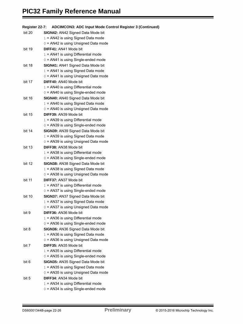
bit 20 SIGN42: AN42 Signed Data Mode bit
1 = AN42 is using Signed Data mode
0 = AN42 is using Unsigned Data mode
bit 19 DIFF41: AN41 Mode bit
1 = AN41 is using Differential mode
0 = AN41 is using Single-ended mode
bit 18 SIGN41: AN41 Signed Data Mode bit
1 = AN41 is using Signed Data mode
0 = AN41 is using Unsigned Data mode
bit 17 DIFF40: AN40 Mode bit
1 = AN40 is using Differential mode
0 = AN40 is using Single-ended mode
bit 16 SIGN40: AN40 Signed Data Mode bit
1 = AN40 is using Signed Data mode
0 = AN40 is using Unsigned Data mode
bit 15 DIFF39: AN39 Mode bit
1 = AN39 is using Differential mode
0 = AN39 is using Single-ended mode
bit 14 SIGN39: AN39 Signed Data Mode bit
1 = AN39 is using Signed Data mode
0 = AN39 is using Unsigned Data mode
bit 13 DIFF38: AN38 Mode bit
1 = AN38 is using Differential mode
0 = AN38 is using Single-ended mode
bit 12 SIGN38: AN38 Signed Data Mode bit
1 = AN38 is using Signed Data mode
0 = AN38 is using Unsigned Data mode
bit 11 DIFF37: AN37 Mode bit
1 = AN37 is using Differential mode
0 = AN37 is using Single-ended mode
bit 10 SIGN37: AN37 Signed Data Mode bit
1 = AN37 is using Signed Data mode
0 = AN37 is using Unsigned Data mode
bit 9 DIFF36: AN36 Mode bit
1 = AN36 is using Differential mode
0 = AN36 is using Single-ended mode
bit 8 SIGN36: AN36 Signed Data Mode bit
1 = AN36 is using Signed Data mode
0 = AN36 is using Unsigned Data mode
bit 7 DIFF35: AN35 Mode bit
1 = AN35 is using Differential mode
0 = AN35 is using Single-ended mode
bit 6 SIGN35: AN35 Signed Data Mode bit
1 = AN35 is using Signed Data mode
0 = AN35 is using Unsigned Data mode
bit 5 DIFF34: AN34 Mode bit
1 = AN34 is using Differential mode
0 = AN34 is using Single-ended mode
Register 22-7: ADCIMCON3: ADC Input Mode Control Register 3 (Continued)
DS60001344B-page 22-26 Preliminary © 2015-2016 Microchip Technology Inc.

Section 22. 12-bit High-Speed SAR ADC
bit 4 SIGN34: AN34 Signed Data Mode bit
1 = AN34 is using Signed Data mode
0 = AN34 is using Unsigned Data mode
bit 3 DIFF33: AN33 Mode bit
1 = AN33 is using Differential mode
0 = AN33 is using Single-ended mode
bit 2 SIGN33: AN33 Signed Data Mode bit
1 = AN33 is using Signed Data mode
0 = AN33 is using Unsigned Data mode
bit 1 DIFF32: AN32 Mode bit
1 = AN32 is using Differential mode
0 = AN32 is using Single-ended mode
bit 0 SIGN32: AN32 Signed Data Mode bit
1 = AN32 is using Signed Data mode
0 = AN32 is using Unsigned Data mode
Register 22-7: ADCIMCON3: ADC Input Mode Control Register 3 (Continued)
© 2015-2016 Microchip Technology Inc. Preliminary DS60001344B-page 22-27

PIC32 Family Reference Manual
Register 22-8: ADCIMCON4: ADC Input Mode Control Register 4
Bit Range Bit31/23/15/7
Bit30/22/14/6
Bit29/21/13/5
Bit28/20/12/4
Bit27/19/11/3
Bit26/18/10/2
Bit25/17/9/1
Bit24/16/8/0
31:24R/W-0 R/W-0 R/W-0 R/W-0 R/W-0 R/W-0 R/W-0 R/W-0
DIFF63 SIGN63 DIFF62 SIGN62 DIFF61 SIGN61 DIFF60 SIGN60
23:16R/W-0 R/W-0 R/W-0 R/W-0 R/W-0 R/W-0 R/W-0 R/W-0
DIFF59 SIGN59 DIFF58 SIGN58 DIFF57 SIGN57 DIFF56 SIGN56
15:8R/W-0 R/W-0 R/W-0 R/W-0 R/W-0 R/W-0 R/W-0 R/W-0
DIFF55 SIGN55 DIFF54 SIGN54 DIFF53 SIGN53 DIFF52 SIGN52
7:0R/W-0 R/W-0 R/W-0 R/W-0 R/W-0 R/W-0 R/W-0 R/W-0
DIFF51 SIGN51 DIFF50 SIGN50 DIFF49 SIGN49 DIFF48 SIGN48
Legend:
R = Readable bit W = Writable bit U = Unimplemented bit, read as ‘0’
-n = Value at POR ‘1’ = Bit is set ‘0’ = Bit is cleared x = Bit is unknown
bit 31 DIFF63: AN63 Mode bit
1 = AN63 is using Differential mode
0 = AN63 is using Single-ended mode
bit 30 SIGN63: AN63 Signed Data Mode bit
1 = AN63 is using Signed Data mode
0 = AN63 is using Unsigned Data mode
bit 29 DIFF62: AN62 Mode bit
1 = AN62 is using Differential mode
0 = AN62 is using Single-ended mode
bit 28 SIGN62: AN62 Signed Data Mode bit
1 = AN62 is using Signed Data mode
0 = AN62 is using Unsigned Data mode
bit 27 DIFF61: AN61 Mode bit
1 = AN61 is using Differential mode
0 = AN61 is using Single-ended mode
bit 26 SIGN61: AN61 Signed Data Mode bit
1 = AN61 is using Signed Data mode
0 = AN61 is using Unsigned Data mode
bit 25 DIFF60: AN60 Mode bit
1 = AN60 is using Differential mode
0 = AN60 is using Single-ended mode
bit 24 SIGN60: AN60 Signed Data Mode bit
1 = AN60 is using Signed Data mode
0 = AN60 is using Unsigned Data mode
bit 23 DIFF59: AN59 Mode bit
1 = AN59 is using Differential mode
0 = AN59 is using Single-ended mode
bit 22 SIGN59: AN59 Signed Data Mode bit
1 = AN59 is using Signed Data mode
0 = AN59 is using Unsigned Data mode
bit 21 DIFF58: AN58 Mode bit
1 = AN58 is using Differential mode
0 = AN58 is using Single-ended mode
DS60001344B-page 22-28 Preliminary © 2015-2016 Microchip Technology Inc.

Section 22. 12-bit High-Speed SAR ADC
bit 20 SIGN58: AN58 Signed Data Mode bit
1 = AN58 is using Signed Data mode
0 = AN58 is using Unsigned Data mode
bit 19 DIFF57: AN57 Mode bit
1 = AN57 is using Differential mode
0 = AN57 is using Single-ended mode
bit 18 SIGN57: AN57 Signed Data Mode bit
1 = AN57 is using Signed Data mode
0 = AN57 is using Unsigned Data mode
bit 17 DIFF56: AN56 Mode bit
1 = AN56 is using Differential mode
0 = AN56 is using Single-ended mode
bit 16 SIGN56: AN56 Signed Data Mode bit
1 = AN56 is using Signed Data mode
0 = AN56 is using Unsigned Data mode
bit 15 DIFF55: AN55 Mode bit
1 = AN55 is using Differential mode
0 = AN55 is using Single-ended mode
bit 14 SIGN55: AN55 Signed Data Mode bit
1 = AN55 is using Signed Data mode
0 = AN55 is using Unsigned Data mode
bit 13 DIFF54: AN54 Mode bit
1 = AN54 is using Differential mode
0 = AN54 is using Single-ended mode
bit 12 SIGN54: AN54 Signed Data Mode bit
1 = AN54 is using Signed Data mode
0 = AN54 is using Unsigned Data mode
bit 11 DIFF53: AN53 Mode bit
1 = AN53 is using Differential mode
0 = AN53 is using Single-ended mode
bit 10 SIGN53: AN53 Signed Data Mode bit
1 = AN53 is using Signed Data mode
0 = AN53 is using Unsigned Data mode
bit 9 DIFF52: AN52 Mode bit
1 = AN52 is using Differential mode
0 = AN52 is using Single-ended mode
bit 8 SIGN52: AN52 Signed Data Mode bit
1 = AN52 is using Signed Data mode
0 = AN52 is using Unsigned Data mode
bit 7 DIFF51: AN51 Mode bit
1 = AN51 is using Differential mode
0 = AN51 is using Single-ended mode
bit 6 SIGN51: AN51 Signed Data Mode bit
1 = AN51 is using Signed Data mode
0 = AN51 is using Unsigned Data mode
bit 5 DIFF50: AN50 Mode bit
1 = AN50 is using Differential mode
0 = AN50 is using Single-ended mode
Register 22-8: ADCIMCON4: ADC Input Mode Control Register 4 (Continued)
© 2015-2016 Microchip Technology Inc. Preliminary DS60001344B-page 22-29

PIC32 Family Reference Manual
bit 4 SIGN50: AN50 Signed Data Mode bit
1 = AN50 is using Signed Data mode
0 = AN50 is using Unsigned Data mode
bit 3 DIFF49: AN49 Mode bit
1 = AN49 is using Differential mode
0 = AN49 is using Single-ended mode
bit 2 SIGN49: AN49 Signed Data Mode bit
1 = AN49 is using Signed Data mode
0 = AN49 is using Unsigned Data mode
bit 1 DIFF48: AN48 Mode bit
1 = AN48 is using Differential mode
0 = AN48 is using Single-ended mode
bit 0 SIGN48: AN48 Signed Data Mode bit
1 = AN48 is using Signed Data mode
0 = AN48 is using Unsigned Data mode
Register 22-8: ADCIMCON4: ADC Input Mode Control Register 4 (Continued)
DS60001344B-page 22-30 Preliminary © 2015-2016 Microchip Technology Inc.

Section 22. 12-bit High-Speed SAR ADC
Register 22-9: ADCGIRQEN1: ADC Global Interrupt Enable Register 1
Bit Range Bit31/23/15/7
Bit30/22/14/6
Bit29/21/13/5
Bit28/20/12/4
Bit27/19/11/3
Bit26/18/10/2
Bit25/17/9/1
Bit24/16/8/0
31:24R/W-0 R/W-0 R/W-0 R/W-0 R/W-0 R/W-0 R/W-0 R/W-0
AGIEN31 AGIEN30 AGIEN29 AGIEN28 AGIEN27 AGIEN26 AGIEN25 AGIEN24
23:16R/W-0 R/W-0 R/W-0 R/W-0 R/W-0 R/W-0 R/W-0 R/W-0
AGIEN23 AGIEN22 AGIEN21 AGIEN20 AGIEN19 AGIEN18 AGIEN17 AGIEN16
15:8R/W-0 R/W-0 R/W-0 R/W-0 R/W-0 R/W-0 R/W-0 R/W-0
AGIEN15 AGIEN14 AGIEN13 AGIEN12 AGIEN11 AGIEN10 AGIEN9 AGIEN8
7:0R/W-0 R/W-0 R/W-0 R/W-0 R/W-0 R/W-0 R/W-0 R/W-0
AGIEN7 AGIEN6 AGIEN5 AGIEN4 AGIEN3 AGIEN2 AGIEN1 AGIEN0
Legend:
R = Readable bit W = Writable bit U = Unimplemented bit, read as ‘0’
-n = Value at POR ‘1’ = Bit is set ‘0’ = Bit is cleared x = Bit is unknown
bit 31-0 AGIEN31:AGIEN0: ADC Interrupt Enable bits
1 = Interrupts are enabled for the selected analog input. The interrupt is generated after the converteddata is ready (indicated by the ARDYx bit (‘x’ = 31-0) of the ADCDSTAT1 register)
0 = Interrupts are disabled
Register 22-10: ADCGIRQEN2: ADC Global Interrupt Enable Register 2
Bit Range Bit31/23/15/7
Bit30/22/14/6
Bit29/21/13/5
Bit28/20/12/4
Bit27/19/11/3
Bit26/18/10/2
Bit25/17/9/1
Bit24/16/8/0
31:24R/W-0 R/W-0 R/W-0 R/W-0 R/W-0 R/W-0 R/W-0 R/W-0
AGIEN63 AGIEN62 AGIEN61 AGIEN60 AGIEN59 AGIEN58 AGIEN57 AGIEN56
23:16R/W-0 R/W-0 R/W-0 R/W-0 R/W-0 R/W-0 R/W-0 R/W-0
AGIEN55 AGIEN54 AGIEN53 AGIEN52 AGIEN51 AGIEN50 AGIEN49 AGIEN48
15:8R/W-0 R/W-0 R/W-0 R/W-0 R/W-0 R/W-0 R/W-0 R/W-0
AGIEN47 AGIEN46 AGIEN45 AGIEN44 AGIEN43 AGIEN42 AGIEN41 AGIEN40
7:0R/W-0 R/W-0 R/W-0 R/W-0 R/W-0 R/W-0 R/W-0 R/W-0
AGIEN39 AGIEN38 AGIEN37 AGIEN36 AGIEN35 AGIEN34 AGIEN33 AGIEN32
Legend:
R = Readable bit W = Writable bit U = Unimplemented bit, read as ‘0’
-n = Value at POR ‘1’ = Bit is set ‘0’ = Bit is cleared x = Bit is unknown
bit 31-0 AGIEN63:AGIEN32 ADC Interrupt Enable bits
1 = Interrupts are enabled for the selected analog input. The interrupt is generated after the converteddata is ready (indicated by the ARDYx bit (‘x’ = 63-32) of the ADCDSTAT2 register)
0 = Interrupts are disabled
© 2015-2016 Microchip Technology Inc. Preliminary DS60001344B-page 22-31
PIC32 Family Reference Manual
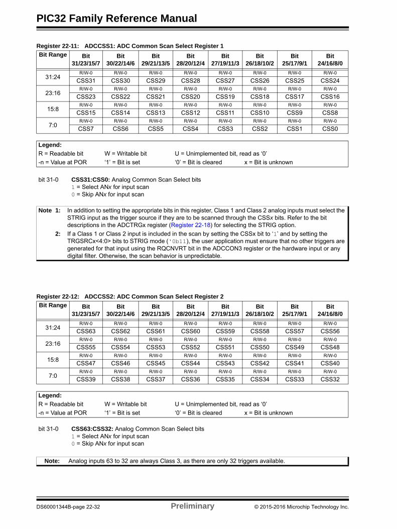
Register 22-11: ADCCSS1: ADC Common Scan Select Register 1
Bit Range Bit31/23/15/7
Bit30/22/14/6
Bit29/21/13/5
Bit28/20/12/4
Bit27/19/11/3
Bit26/18/10/2
Bit25/17/9/1
Bit24/16/8/0
31:24R/W-0 R/W-0 R/W-0 R/W-0 R/W-0 R/W-0 R/W-0 R/W-0
CSS31 CSS30 CSS29 CSS28 CSS27 CSS26 CSS25 CSS24
23:16R/W-0 R/W-0 R/W-0 R/W-0 R/W-0 R/W-0 R/W-0 R/W-0
CSS23 CSS22 CSS21 CSS20 CSS19 CSS18 CSS17 CSS16
15:8R/W-0 R/W-0 R/W-0 R/W-0 R/W-0 R/W-0 R/W-0 R/W-0
CSS15 CSS14 CSS13 CSS12 CSS11 CSS10 CSS9 CSS8
7:0R/W-0 R/W-0 R/W-0 R/W-0 R/W-0 R/W-0 R/W-0 R/W-0
CSS7 CSS6 CSS5 CSS4 CSS3 CSS2 CSS1 CSS0
Legend:
R = Readable bit W = Writable bit U = Unimplemented bit, read as ‘0’
-n = Value at POR ‘1’ = Bit is set ‘0’ = Bit is cleared x = Bit is unknown
bit 31-0 CSS31:CSS0: Analog Common Scan Select bits1 = Select ANx for input scan0 = Skip ANx for input scan
Note 1: In addition to setting the appropriate bits in this register, Class 1 and Class 2 analog inputs must select the STRIG input as the trigger source if they are to be scanned through the CSSx bits. Refer to the bit descriptions in the ADCTRGx register (Register 22-18) for selecting the STRIG option.
2: If a Class 1 or Class 2 input is included in the scan by setting the CSSx bit to ‘1’ and by setting the TRGSRCx<4:0> bits to STRIG mode (‘0b11), the user application must ensure that no other triggers are generated for that input using the RQCNVRT bit in the ADCCON3 register or the hardware input or any digital filter. Otherwise, the scan behavior is unpredictable.
Register 22-12: ADCCSS2: ADC Common Scan Select Register 2
Bit Range Bit31/23/15/7
Bit30/22/14/6
Bit29/21/13/5
Bit28/20/12/4
Bit27/19/11/3
Bit26/18/10/2
Bit25/17/9/1
Bit24/16/8/0
31:24R/W-0 R/W-0 R/W-0 R/W-0 R/W-0 R/W-0 R/W-0 R/W-0
CSS63 CSS62 CSS61 CSS60 CSS59 CSS58 CSS57 CSS56
23:16R/W-0 R/W-0 R/W-0 R/W-0 R/W-0 R/W-0 R/W-0 R/W-0
CSS55 CSS54 CSS53 CSS52 CSS51 CSS50 CSS49 CSS48
15:8R/W-0 R/W-0 R/W-0 R/W-0 R/W-0 R/W-0 R/W-0 R/W-0
CSS47 CSS46 CSS45 CSS44 CSS43 CSS42 CSS41 CSS40
7:0R/W-0 R/W-0 R/W-0 R/W-0 R/W-0 R/W-0 R/W-0 R/W-0
CSS39 CSS38 CSS37 CSS36 CSS35 CSS34 CSS33 CSS32
Legend:
R = Readable bit W = Writable bit U = Unimplemented bit, read as ‘0’
-n = Value at POR ‘1’ = Bit is set ‘0’ = Bit is cleared x = Bit is unknown
bit 31-0 CSS63:CSS32: Analog Common Scan Select bits1 = Select ANx for input scan0 = Skip ANx for input scan
Note: Analog inputs 63 to 32 are always Class 3, as there are only 32 triggers available.
DS60001344B-page 22-32 Preliminary © 2015-2016 Microchip Technology Inc.
Section 22. 12-bit High-Speed SAR ADC
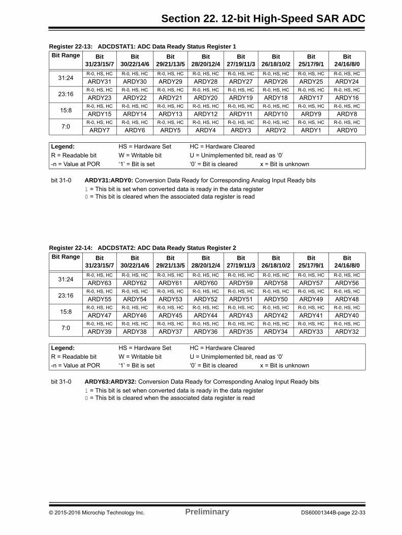
Register 22-13: ADCDSTAT1: ADC Data Ready Status Register 1
Bit Range Bit31/23/15/7
Bit30/22/14/6
Bit29/21/13/5
Bit28/20/12/4
Bit27/19/11/3
Bit26/18/10/2
Bit25/17/9/1
Bit24/16/8/0
31:24R-0, HS, HC R-0, HS, HC R-0, HS, HC R-0, HS, HC R-0, HS, HC R-0, HS, HC R-0, HS, HC R-0, HS, HC
ARDY31 ARDY30 ARDY29 ARDY28 ARDY27 ARDY26 ARDY25 ARDY24
23:16R-0, HS, HC R-0, HS, HC R-0, HS, HC R-0, HS, HC R-0, HS, HC R-0, HS, HC R-0, HS, HC R-0, HS, HC
ARDY23 ARDY22 ARDY21 ARDY20 ARDY19 ARDY18 ARDY17 ARDY16
15:8R-0, HS, HC R-0, HS, HC R-0, HS, HC R-0, HS, HC R-0, HS, HC R-0, HS, HC R-0, HS, HC R-0, HS, HC
ARDY15 ARDY14 ARDY13 ARDY12 ARDY11 ARDY10 ARDY9 ARDY8
7:0R-0, HS, HC R-0, HS, HC R-0, HS, HC R-0, HS, HC R-0, HS, HC R-0, HS, HC R-0, HS, HC R-0, HS, HC
ARDY7 ARDY6 ARDY5 ARDY4 ARDY3 ARDY2 ARDY1 ARDY0
Legend: HS = Hardware Set HC = Hardware Cleared
R = Readable bit W = Writable bit U = Unimplemented bit, read as ‘0’
-n = Value at POR ‘1’ = Bit is set ‘0’ = Bit is cleared x = Bit is unknown
bit 31-0 ARDY31:ARDY0: Conversion Data Ready for Corresponding Analog Input Ready bits
1 = This bit is set when converted data is ready in the data register0 = This bit is cleared when the associated data register is read
Register 22-14: ADCDSTAT2: ADC Data Ready Status Register 2
Bit Range Bit31/23/15/7
Bit30/22/14/6
Bit29/21/13/5
Bit28/20/12/4
Bit27/19/11/3
Bit26/18/10/2
Bit25/17/9/1
Bit24/16/8/0
31:24R-0, HS, HC R-0, HS, HC R-0, HS, HC R-0, HS, HC R-0, HS, HC R-0, HS, HC R-0, HS, HC R-0, HS, HC
ARDY63 ARDY62 ARDY61 ARDY60 ARDY59 ARDY58 ARDY57 ARDY56
23:16R-0, HS, HC R-0, HS, HC R-0, HS, HC R-0, HS, HC R-0, HS, HC R-0, HS, HC R-0, HS, HC R-0, HS, HC
ARDY55 ARDY54 ARDY53 ARDY52 ARDY51 ARDY50 ARDY49 ARDY48
15:8R-0, HS, HC R-0, HS, HC R-0, HS, HC R-0, HS, HC R-0, HS, HC R-0, HS, HC R-0, HS, HC R-0, HS, HC
ARDY47 ARDY46 ARDY45 ARDY44 ARDY43 ARDY42 ARDY41 ARDY40
7:0R-0, HS, HC R-0, HS, HC R-0, HS, HC R-0, HS, HC R-0, HS, HC R-0, HS, HC R-0, HS, HC R-0, HS, HC
ARDY39 ARDY38 ARDY37 ARDY36 ARDY35 ARDY34 ARDY33 ARDY32
Legend: HS = Hardware Set HC = Hardware Cleared
R = Readable bit W = Writable bit U = Unimplemented bit, read as ‘0’
-n = Value at POR ‘1’ = Bit is set ‘0’ = Bit is cleared x = Bit is unknown
bit 31-0 ARDY63:ARDY32: Conversion Data Ready for Corresponding Analog Input Ready bits
1 = This bit is set when converted data is ready in the data register0 = This bit is cleared when the associated data register is read
© 2015-2016 Microchip Technology Inc. Preliminary DS60001344B-page 22-33
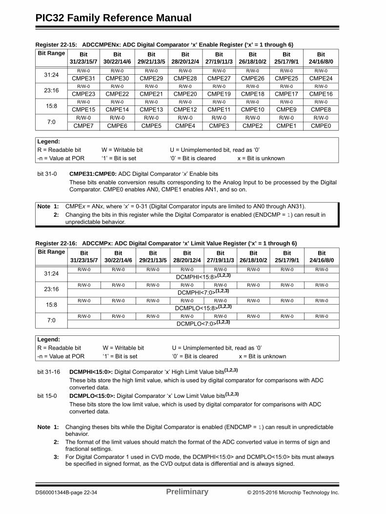
PIC32 Family Reference Manual
Register 22-15: ADCCMPENx: ADC Digital Comparator ‘x’ Enable Register (‘x’ = 1 through 6)
Bit Range Bit31/23/15/7
Bit30/22/14/6
Bit29/21/13/5
Bit28/20/12/4
Bit27/19/11/3
Bit26/18/10/2
Bit25/17/9/1
Bit24/16/8/0
31:24R/W-0 R/W-0 R/W-0 R/W-0 R/W-0 R/W-0 R/W-0 R/W-0
CMPE31 CMPE30 CMPE29 CMPE28 CMPE27 CMPE26 CMPE25 CMPE24
23:16R/W-0 R/W-0 R/W-0 R/W-0 R/W-0 R/W-0 R/W-0 R/W-0
CMPE23 CMPE22 CMPE21 CMPE20 CMPE19 CMPE18 CMPE17 CMPE16
15:8R/W-0 R/W-0 R/W-0 R/W-0 R/W-0 R/W-0 R/W-0 R/W-0
CMPE15 CMPE14 CMPE13 CMPE12 CMPE11 CMPE10 CMPE9 CMPE8
7:0R/W-0 R/W-0 R/W-0 R/W-0 R/W-0 R/W-0 R/W-0 R/W-0
CMPE7 CMPE6 CMPE5 CMPE4 CMPE3 CMPE2 CMPE1 CMPE0
Legend:
R = Readable bit W = Writable bit U = Unimplemented bit, read as ‘0’
-n = Value at POR ‘1’ = Bit is set ‘0’ = Bit is cleared x = Bit is unknown
bit 31-0 CMPE31:CMPE0: ADC Digital Comparator ‘x’ Enable bits
These bits enable conversion results corresponding to the Analog Input to be processed by the DigitalComparator. CMPE0 enables AN0, CMPE1 enables AN1, and so on.
Note 1: CMPEx = ANx, where ‘x’ = 0-31 (Digital Comparator inputs are limited to AN0 through AN31).
2: Changing the bits in this register while the Digital Comparator is enabled (ENDCMP = 1) can result in unpredictable behavior.
Register 22-16: ADCCMPx: ADC Digital Comparator ‘x’ Limit Value Register (‘x’ = 1 through 6)
Bit Range Bit31/23/15/7
Bit30/22/14/6
Bit29/21/13/5
Bit28/20/12/4
Bit27/19/11/3
Bit26/18/10/2
Bit25/17/9/1
Bit24/16/8/0
31:24R/W-0 R/W-0 R/W-0 R/W-0 R/W-0 R/W-0 R/W-0 R/W-0
DCMPHI<15:8>(1,2,3)
23:16R/W-0 R/W-0 R/W-0 R/W-0 R/W-0 R/W-0 R/W-0 R/W-0
DCMPHI<7:0>(1,2,3)
15:8R/W-0 R/W-0 R/W-0 R/W-0 R/W-0 R/W-0 R/W-0 R/W-0
DCMPLO<15:8>(1,2,3)
7:0R/W-0 R/W-0 R/W-0 R/W-0 R/W-0 R/W-0 R/W-0 R/W-0
DCMPLO<7:0>(1,2,3)
Legend:
R = Readable bit W = Writable bit U = Unimplemented bit, read as ‘0’
-n = Value at POR ‘1’ = Bit is set ‘0’ = Bit is cleared x = Bit is unknown
bit 31-16 DCMPHI<15:0>: Digital Comparator ‘x’ High Limit Value bits(1,2,3)
These bits store the high limit value, which is used by digital comparator for comparisons with ADC converted data.
bit 15-0 DCMPLO<15:0>: Digital Comparator ‘x’ Low Limit Value bits(1,2,3)
These bits store the low limit value, which is used by digital comparator for comparisons with ADC converted data.
Note 1: Changing theses bits while the Digital Comparator is enabled (ENDCMP = 1) can result in unpredictable behavior.
2: The format of the limit values should match the format of the ADC converted value in terms of sign and fractional settings.
3: For Digital Comparator 1 used in CVD mode, the DCMPHI<15:0> and DCMPLO<15:0> bits must always be specified in signed format, as the CVD output data is differential and is always signed.
DS60001344B-page 22-34 Preliminary © 2015-2016 Microchip Technology Inc.

Section 22. 12-bit High-Speed SAR ADC
Register 22-17: ADCFLTRx: ADC Digital Filter ‘x’ Register (‘x’ = 1 through 6)
Bit Range
Bit31/23/15/7
Bit30/22/14/6
Bit29/21/13/5
Bit28/20/12/4
Bit27/19/11/3
Bit26/18/10/2
Bit25/17/9/1
Bit24/16/8/0
31:24R/W-0 R/W-0 R/W-0 R/W-0 R/W-0 R/W-0 R/W-0 R-0, HS, HC
AFEN DATA16EN DFMODE OVRSAM<2:0> AFGIEN AFRDY
23:16U-0 U-0 U-0 R/W-0 R/W-0 R/W-0 R/W-0 R/W-0
— — — CHNLID<4:0>
15:8R-0, HS, HC R-0, HS, HC R-0, HS, HC R-0, HS, HC R-0, HS, HC R-0, HS, HC R-0, HS, HC R-0, HS, HC
FLTRDATA<15:8>
7:0R-0, HS, HC R-0, HS, HC R-0, HS, HC R-0, HS, HC R-0, HS, HC R-0, HS, HC R-0, HS, HC R-0, HS, HC
FLTRDATA<7:0>
Legend: HS = Hardware Set HC = Hardware Cleared
R = Readable bit W = Writable bit U = Unimplemented bit, read as ‘0’
-n = Value at POR ‘1’ = Bit is set ‘0’ = Bit is cleared x = Bit is unknown
bit 31 AFEN: Digital Filter ‘x’ Enable bit1 = Digital filter is enabled0 = Digital filter is disabled and the AFRDY status bit is cleared
bit 30 DATA16EN: Filter Significant Data Length bit
1 = All 16 bits of the filter output data are significant0 = Only the first 12 bits are significant, followed by four zeros
Note: This bit is significant only if DFMODE = 1 (Averaging Mode) and FRACT (ADCCON1<23>) = 1(Fractional Output Mode).
bit 29 DFMODE: ADC Filter Mode bit
1 = Filter ‘x’ works in Averaging mode0 = Filter ‘x’ works in Oversampling Filter mode (default)
When the ADC filter is enabled and DFMODE = 0:
Once an ADC edge conversion trigger event occurs, it is held active until the filter OVRSAM sample count has expired.
The Minimum Trigger Period = (OVRSAM<2:0> bits in ADCFLTRx) (SAMC<7:0> bits in ADCxTIME TAD +((SELRES<1:0> bits in ADCxTIME + 1) TAD).
Example:
• OVRSAM<2:0> bits in ADCFLTRx = 8x Samples
• SAMC<7:0> bits in ADCxTIME = 3 TAD
• SELRES<1:0> bits in ADCxTIME = 12 bits
User Min Trig period ≥ (8 * (3 TAD + 13 TAD)) = 128 TAD
When the ADC filter is enabled and DFMODE = 1:
All ADC conversions are initiated solely by trigger events. After OVRSAM normal edge trigger events andsubsequent conversions, the ADC filter result will contain the average value of OVRSAM number ofconversions.
Refer to Figure 22-18: “ADC Filter Comparisons Example” for more information.
© 2015-2016 Microchip Technology Inc. Preliminary DS60001344B-page 22-35
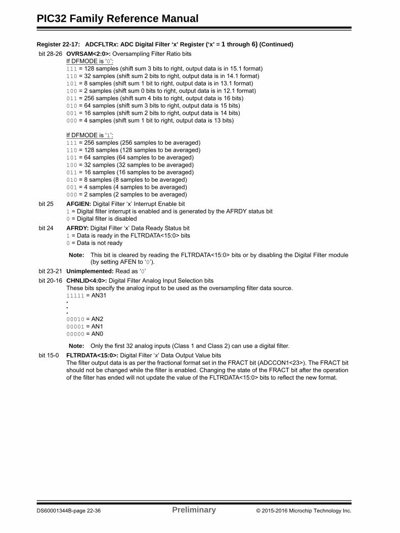
PIC32 Family Reference Manual
bit 28-26 OVRSAM<2:0>: Oversampling Filter Ratio bitsIf DFMODE is ‘0’:111 = 128 samples (shift sum 3 bits to right, output data is in 15.1 format)110 = 32 samples (shift sum 2 bits to right, output data is in 14.1 format)101 = 8 samples (shift sum 1 bit to right, output data is in 13.1 format)100 = 2 samples (shift sum 0 bits to right, output data is in 12.1 format)011 = 256 samples (shift sum 4 bits to right, output data is 16 bits)010 = 64 samples (shift sum 3 bits to right, output data is 15 bits)001 = 16 samples (shift sum 2 bits to right, output data is 14 bits)000 = 4 samples (shift sum 1 bit to right, output data is 13 bits)
If DFMODE is ‘1’:111 = 256 samples (256 samples to be averaged)110 = 128 samples (128 samples to be averaged)101 = 64 samples (64 samples to be averaged)100 = 32 samples (32 samples to be averaged)011 = 16 samples (16 samples to be averaged)010 = 8 samples (8 samples to be averaged)001 = 4 samples (4 samples to be averaged)000 = 2 samples (2 samples to be averaged)
bit 25 AFGIEN: Digital Filter ‘x’ Interrupt Enable bit1 = Digital filter interrupt is enabled and is generated by the AFRDY status bit0 = Digital filter is disabled
bit 24 AFRDY: Digital Filter ‘x’ Data Ready Status bit1 = Data is ready in the FLTRDATA<15:0> bits0 = Data is not ready
Note: This bit is cleared by reading the FLTRDATA<15:0> bits or by disabling the Digital Filter module(by setting AFEN to ‘0’).
bit 23-21 Unimplemented: Read as ‘0’
bit 20-16 CHNLID<4:0>: Digital Filter Analog Input Selection bitsThese bits specify the analog input to be used as the oversampling filter data source.11111 = AN31•••00010 = AN200001 = AN100000 = AN0
Note: Only the first 32 analog inputs (Class 1 and Class 2) can use a digital filter.
bit 15-0 FLTRDATA<15:0>: Digital Filter ‘x’ Data Output Value bitsThe filter output data is as per the fractional format set in the FRACT bit (ADCCON1<23>). The FRACT bitshould not be changed while the filter is enabled. Changing the state of the FRACT bit after the operationof the filter has ended will not update the value of the FLTRDATA<15:0> bits to reflect the new format.
Register 22-17: ADCFLTRx: ADC Digital Filter ‘x’ Register (‘x’ = 1 through 6) (Continued)
DS60001344B-page 22-36 Preliminary © 2015-2016 Microchip Technology Inc.

Section 22. 12-bit High-Speed SAR ADC
Register 22-18: ADCTRG1: ADC Trigger Source 1Register
Bit Range
Bit31/23/15/7
Bit30/22/14/6
Bit29/21/13/5
Bit28/20/12/4
Bit27/19/11/3
Bit26/18/10/2
Bit25/17/9/1
Bit24/16/8/0
31:24U-0 U-0 U-0 R/W-0 R/W-0 R/W-0 R/W-0 R/W-0
— — — TRGSRC3<4:0>
23:16U-0 U-0 U-0 R/W-0 R/W-0 R/W-0 R/W-0 R/W-0
— — — TRGSRC2<4:0>
15:8U-0 U-0 U-0 R/W-0 R/W-0 R/W-0 R/W-0 R/W-0
— — — TRGSRC1<4:0>
7:0U-0 U-0 U-0 R/W-0 R/W-0 R/W-0 R/W-0 R/W-0
— — — TRGSRC0<4:0>
Legend:
R = Readable bit W = Writable bit U = Unimplemented bit, read as ‘0’
-n = Value at POR ‘1’ = Bit is set ‘0’ = Bit is cleared x = Bit is unknown
bit 31-29 Unimplemented: Read as ‘0’
bit 28-24 TRGSRC3<4:0>: Trigger Source for Conversion of Analog Input AN3 Select bits11111 - 00100 = Refer to the “ADC” chapter in the specific device data sheet for trigger source selections00011 = Scan Trigger (STRIG)00010 = Global level software trigger (GLSWTRG)00001 = Global software edge Trigger (GSWTRG)00000 = No Trigger
For STRIG, in addition to setting the trigger, it also requires programming of the STRGSRC<4:0> bits(ADCCON1<20:16>) to select the trigger source, and requires the appropriate CSSx bits to be set in theADCCSSx registers.
bit 23-21 Unimplemented: Read as ‘0’
bit 20-16 TRGSRC2<4:0>: Trigger Source for Conversion of Analog Input AN2 Select bitsSee bits 28-24 for bit value definitions.
bit 15-13 Unimplemented: Read as ‘0’
bit 12-8 TRGSRC1<4:0>: Trigger Source for Conversion of Analog Input AN1 Select bitsSee bits 28-24 for bit value definitions.
bit 7-5 Unimplemented: Read as ‘0’
bit 4-0 TRGSRC0<4:0>: Trigger Source for Conversion of Analog Input AN0 Select bitsSee bits 28-24 for bit value definitions.
© 2015-2016 Microchip Technology Inc. Preliminary DS60001344B-page 22-37

PIC32 Family Reference Manual
Register 22-19: ADCTRG2: ADC Trigger Source 2 Register
Bit Range
Bit31/23/15/7
Bit30/22/14/6
Bit29/21/13/5
Bit28/20/12/4
Bit27/19/11/3
Bit26/18/10/2
Bit25/17/9/1
Bit24/16/8/0
31:24U-0 U-0 U-0 R/W-0 R/W-0 R/W-0 R/W-0 R/W-0
— — — TRGSRC7<4:0>
23:16U-0 U-0 U-0 R/W-0 R/W-0 R/W-0 R/W-0 R/W-0
— — — TRGSRC6<4:0>
15:8U-0 U-0 U-0 R/W-0 R/W-0 R/W-0 R/W-0 R/W-0
— — — TRGSRC5<4:0>
7:0U-0 U-0 U-0 R/W-0 R/W-0 R/W-0 R/W-0 R/W-0
— — — TRGSRC4<4:0>
Legend:
R = Readable bit W = Writable bit U = Unimplemented bit, read as ‘0’
-n = Value at POR ‘1’ = Bit is set ‘0’ = Bit is cleared x = Bit is unknown
bit 31-29 Unimplemented: Read as ‘0’
bit 28-24 TRGSRC7<4:0>: Trigger Source for Conversion of Analog Input AN7 Select bits11111 - 00100 = Refer to the “ADC” chapter in the specific device data sheet for trigger source selections00011 = Scan Trigger (STRIG)00010 = Global level software trigger (GLSWTRG)00001 = Global software edge Trigger (GSWTRG)00000 = No Trigger
For STRIG, in addition to setting the trigger, it also requires programming of the STRGSRC<4:0> bits(ADCCON1<20:16>) to select the trigger source, and requires the appropriate CSSx bits to be set in theADCCSSx registers.
bit 23-21 Unimplemented: Read as ‘0’
bit 20-16 TRGSRC6<4:0>: Trigger Source for Conversion of Analog Input AN6 Select bitsSee bits 28-24 for bit value definitions.
bit 15-13 Unimplemented: Read as ‘0’
bit 12-8 TRGSRC5<4:0>: Trigger Source for Conversion of Analog Input AN5 Select bitsSee bits 28-24 for bit value definitions.
bit 7-5 Unimplemented: Read as ‘0’
bit 4-0 TRGSRC4<4:0>: Trigger Source for Conversion of Analog Input AN4 Select bitsSee bits 28-24 for bit value definitions.
DS60001344B-page 22-38 Preliminary © 2015-2016 Microchip Technology Inc.

Section 22. 12-bit High-Speed SAR ADC
Register 22-20: ADCTRG3: ADC Trigger Source 3 Register
Bit Range
Bit31/23/15/7
Bit30/22/14/6
Bit29/21/13/5
Bit28/20/12/4
Bit27/19/11/3
Bit26/18/10/2
Bit25/17/9/1
Bit24/16/8/0
31:24U-0 U-0 U-0 R/W-0 R/W-0 R/W-0 R/W-0 R/W-0
— — — TRGSRC11<4:0>
23:16U-0 U-0 U-0 R/W-0 R/W-0 R/W-0 R/W-0 R/W-0
— — — TRGSRC10<4:0>
15:8U-0 U-0 U-0 R/W-0 R/W-0 R/W-0 R/W-0 R/W-0
— — — TRGSRC9<4:0>
7:0U-0 U-0 U-0 R/W-0 R/W-0 R/W-0 R/W-0 R/W-0
— — — TRGSRC8<4:0>
Legend:
R = Readable bit W = Writable bit U = Unimplemented bit, read as ‘0’
-n = Value at POR ‘1’ = Bit is set ‘0’ = Bit is cleared x = Bit is unknown
bit 31-29 Unimplemented: Read as ‘0’
bit 28-24 TRGSRC11<4:0>: Trigger Source for Conversion of Analog Input AN11 Select bits11111 - 00100 = Refer to the “ADC” chapter in the specific device data sheet for trigger source selections00011 = Scan Trigger (STRIG)00010 = Global level software trigger (GLSWTRG)00001 = Global software edge Trigger (GSWTRG)00000 = No Trigger
For STRIG, in addition to setting the trigger, it also requires programming of the STRGSRC<4:0> bits(ADCCON1<20:16>) to select the trigger source, and requires the appropriate CSSx bits to be set in theADCCSSx registers.
bit 23-21 Unimplemented: Read as ‘0’
bit 20-16 TRGSRC10<4:0>: Trigger Source for Conversion of Analog Input AN10 Select bitsSee bits 28-24 for bit value definitions.
bit 15-13 Unimplemented: Read as ‘0’
bit 12-8 TRGSRC9<4:0>: Trigger Source for Conversion of Analog Input AN9 Select bitsSee bits 28-24 for bit value definitions.
bit 7-5 Unimplemented: Read as ‘0’
bit 4-0 TRGSRC8<4:0>: Trigger Source for Conversion of Analog Input AN8 Select bitsSee bits 28-24 for bit value definitions.
© 2015-2016 Microchip Technology Inc. Preliminary DS60001344B-page 22-39
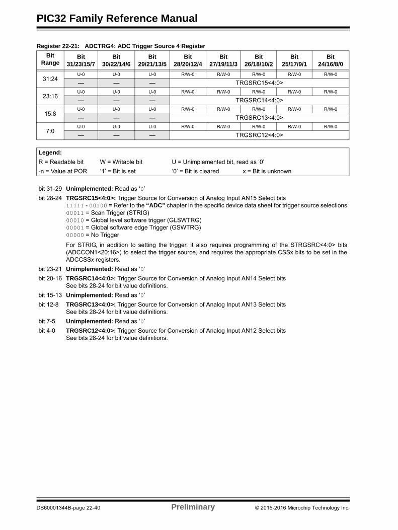
PIC32 Family Reference Manual
Register 22-21: ADCTRG4: ADC Trigger Source 4 Register
Bit Range
Bit31/23/15/7
Bit30/22/14/6
Bit29/21/13/5
Bit28/20/12/4
Bit27/19/11/3
Bit26/18/10/2
Bit25/17/9/1
Bit24/16/8/0
31:24U-0 U-0 U-0 R/W-0 R/W-0 R/W-0 R/W-0 R/W-0
— — — TRGSRC15<4:0>
23:16U-0 U-0 U-0 R/W-0 R/W-0 R/W-0 R/W-0 R/W-0
— — — TRGSRC14<4:0>
15:8U-0 U-0 U-0 R/W-0 R/W-0 R/W-0 R/W-0 R/W-0
— — — TRGSRC13<4:0>
7:0U-0 U-0 U-0 R/W-0 R/W-0 R/W-0 R/W-0 R/W-0
— — — TRGSRC12<4:0>
Legend:
R = Readable bit W = Writable bit U = Unimplemented bit, read as ‘0’
-n = Value at POR ‘1’ = Bit is set ‘0’ = Bit is cleared x = Bit is unknown
bit 31-29 Unimplemented: Read as ‘0’
bit 28-24 TRGSRC15<4:0>: Trigger Source for Conversion of Analog Input AN15 Select bits11111 - 00100 = Refer to the “ADC” chapter in the specific device data sheet for trigger source selections00011 = Scan Trigger (STRIG)00010 = Global level software trigger (GLSWTRG)00001 = Global software edge Trigger (GSWTRG)00000 = No Trigger
For STRIG, in addition to setting the trigger, it also requires programming of the STRGSRC<4:0> bits(ADCCON1<20:16>) to select the trigger source, and requires the appropriate CSSx bits to be set in theADCCSSx registers.
bit 23-21 Unimplemented: Read as ‘0’
bit 20-16 TRGSRC14<4:0>: Trigger Source for Conversion of Analog Input AN14 Select bitsSee bits 28-24 for bit value definitions.
bit 15-13 Unimplemented: Read as ‘0’
bit 12-8 TRGSRC13<4:0>: Trigger Source for Conversion of Analog Input AN13 Select bitsSee bits 28-24 for bit value definitions.
bit 7-5 Unimplemented: Read as ‘0’
bit 4-0 TRGSRC12<4:0>: Trigger Source for Conversion of Analog Input AN12 Select bitsSee bits 28-24 for bit value definitions.
DS60001344B-page 22-40 Preliminary © 2015-2016 Microchip Technology Inc.
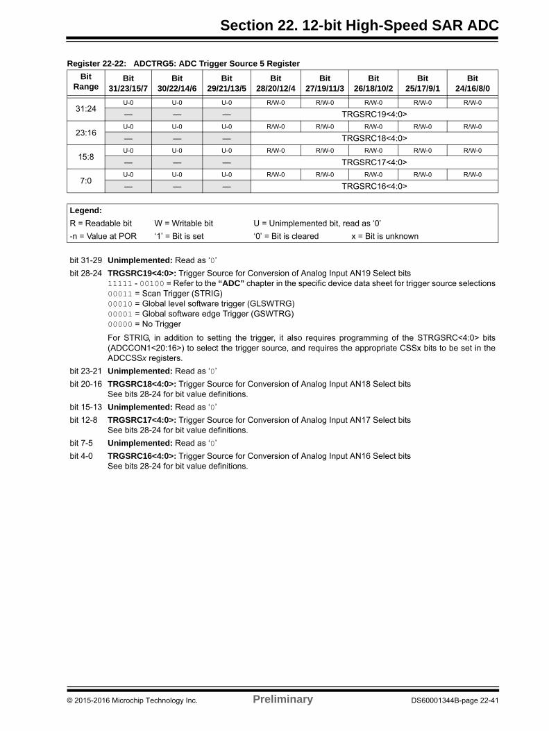
Section 22. 12-bit High-Speed SAR ADC
Register 22-22: ADCTRG5: ADC Trigger Source 5 Register
Bit Range
Bit31/23/15/7
Bit30/22/14/6
Bit29/21/13/5
Bit28/20/12/4
Bit27/19/11/3
Bit26/18/10/2
Bit25/17/9/1
Bit24/16/8/0
31:24U-0 U-0 U-0 R/W-0 R/W-0 R/W-0 R/W-0 R/W-0
— — — TRGSRC19<4:0>
23:16U-0 U-0 U-0 R/W-0 R/W-0 R/W-0 R/W-0 R/W-0
— — — TRGSRC18<4:0>
15:8U-0 U-0 U-0 R/W-0 R/W-0 R/W-0 R/W-0 R/W-0
— — — TRGSRC17<4:0>
7:0U-0 U-0 U-0 R/W-0 R/W-0 R/W-0 R/W-0 R/W-0
— — — TRGSRC16<4:0>
Legend:
R = Readable bit W = Writable bit U = Unimplemented bit, read as ‘0’
-n = Value at POR ‘1’ = Bit is set ‘0’ = Bit is cleared x = Bit is unknown
bit 31-29 Unimplemented: Read as ‘0’
bit 28-24 TRGSRC19<4:0>: Trigger Source for Conversion of Analog Input AN19 Select bits11111 - 00100 = Refer to the “ADC” chapter in the specific device data sheet for trigger source selections00011 = Scan Trigger (STRIG)00010 = Global level software trigger (GLSWTRG)00001 = Global software edge Trigger (GSWTRG)00000 = No Trigger
For STRIG, in addition to setting the trigger, it also requires programming of the STRGSRC<4:0> bits(ADCCON1<20:16>) to select the trigger source, and requires the appropriate CSSx bits to be set in theADCCSSx registers.
bit 23-21 Unimplemented: Read as ‘0’
bit 20-16 TRGSRC18<4:0>: Trigger Source for Conversion of Analog Input AN18 Select bitsSee bits 28-24 for bit value definitions.
bit 15-13 Unimplemented: Read as ‘0’
bit 12-8 TRGSRC17<4:0>: Trigger Source for Conversion of Analog Input AN17 Select bitsSee bits 28-24 for bit value definitions.
bit 7-5 Unimplemented: Read as ‘0’
bit 4-0 TRGSRC16<4:0>: Trigger Source for Conversion of Analog Input AN16 Select bitsSee bits 28-24 for bit value definitions.
© 2015-2016 Microchip Technology Inc. Preliminary DS60001344B-page 22-41

PIC32 Family Reference Manual
Register 22-23: ADCTRG6: ADC Trigger Source 6 Register
Bit Range
Bit31/23/15/7
Bit30/22/14/6
Bit29/21/13/5
Bit28/20/12/4
Bit27/19/11/3
Bit26/18/10/2
Bit25/17/9/1
Bit24/16/8/0
31:24U-0 U-0 U-0 R/W-0 R/W-0 R/W-0 R/W-0 R/W-0
— — — TRGSRC23<4:0>
23:16U-0 U-0 U-0 R/W-0 R/W-0 R/W-0 R/W-0 R/W-0
— — — TRGSRC22<4:0>
15:8U-0 U-0 U-0 R/W-0 R/W-0 R/W-0 R/W-0 R/W-0
— — — TRGSRC21<4:0>
7:0U-0 U-0 U-0 R/W-0 R/W-0 R/W-0 R/W-0 R/W-0
— — — TRGSRC20<4:0>
Legend:
R = Readable bit W = Writable bit U = Unimplemented bit, read as ‘0’
-n = Value at POR ‘1’ = Bit is set ‘0’ = Bit is cleared x = Bit is unknown
bit 31-29 Unimplemented: Read as ‘0’
bit 28-24 TRGSRC23<4:0>: Trigger Source for Conversion of Analog Input AN23 Select bits11111-00100 = Refer to the “ADC” chapter in the specific device data sheet for information00011 = Scan Trigger (STRIG)00010 = Global level software trigger (GLSWTRG)00001 = Global software edge Trigger (GSWTRG)00000 = No Trigger
For STRIG, in addition to setting the trigger, it also requires programming of the STRGSRC<4:0> bits(ADCCON1<20:16>) to select the trigger source, and requires the appropriate CSSx bits to be set in theADCCSSx registers.
bit 23-21 Unimplemented: Read as ‘0’
bit 20-16 TRGSRC22<4:0>: Trigger Source for Conversion of Analog Input AN22 Select bitsSee bits 28-24 for bit value definitions.
bit 15-13 Unimplemented: Read as ‘0’
bit 12-8 TRGSRC21<4:0>: Trigger Source for Conversion of Analog Input AN21 Select bitsSee bits 28-24 for bit value definitions.
bit 7-5 Unimplemented: Read as ‘0’
bit 4-0 TRGSRC20<4:0>: Trigger Source for Conversion of Analog Input AN20 Select bitsSee bits 28-24 for bit value definitions.
DS60001344B-page 22-42 Preliminary © 2015-2016 Microchip Technology Inc.

Section 22. 12-bit High-Speed SAR ADC
Register 22-24: ADCTRG7: ADC Trigger Source 7 Register
Bit Range
Bit31/23/15/7
Bit30/22/14/6
Bit29/21/13/5
Bit28/20/12/4
Bit27/19/11/3
Bit26/18/10/2
Bit25/17/9/1
Bit24/16/8/0
31:24U-0 U-0 U-0 R/W-0 R/W-0 R/W-0 R/W-0 R/W-0
— — — TRGSRC27<4:0>
23:16U-0 U-0 U-0 R/W-0 R/W-0 R/W-0 R/W-0 R/W-0
— — — TRGSRC26<4:0>
15:8U-0 U-0 U-0 R/W-0 R/W-0 R/W-0 R/W-0 R/W-0
— — — TRGSRC25<4:0>
7:0U-0 U-0 U-0 R/W-0 R/W-0 R/W-0 R/W-0 R/W-0
— — — TRGSRC24<4:0>
Legend:
R = Readable bit W = Writable bit U = Unimplemented bit, read as ‘0’
-n = Value at POR ‘1’ = Bit is set ‘0’ = Bit is cleared x = Bit is unknown
bit 31-29 Unimplemented: Read as ‘0’
bit 28-24 TRGSRC27<4:0>: Trigger Source for Conversion of Analog Input AN27 Select bits11111-00100 = Refer to the “ADC” chapter in the specific device data sheet for information00011 = Scan Trigger (STRIG)00010 = Global level software trigger (GLSWTRG)00001 = Global software edge Trigger (GSWTRG)00000 = No Trigger
For STRIG, in addition to setting the trigger, it also requires programming of the STRGSRC<4:0> bits(ADCCON1<20:16>) to select the trigger source, and requires the appropriate CSSx bits to be set in theADCCSSx registers.
bit 23-21 Unimplemented: Read as ‘0’
bit 20-16 TRGSRC26<4:0>: Trigger Source for Conversion of Analog Input AN26 Select bitsSee bits 28-24 for bit value definitions.
bit 15-13 Unimplemented: Read as ‘0’
bit 12-8 TRGSRC25<4:0>: Trigger Source for Conversion of Analog Input AN25 Select bitsSee bits 28-24 for bit value definitions.
bit 7-5 Unimplemented: Read as ‘0’
bit 4-0 TRGSRC24<4:0>: Trigger Source for Conversion of Analog Input AN24 Select bitsSee bits 28-24 for bit value definitions.
© 2015-2016 Microchip Technology Inc. Preliminary DS60001344B-page 22-43
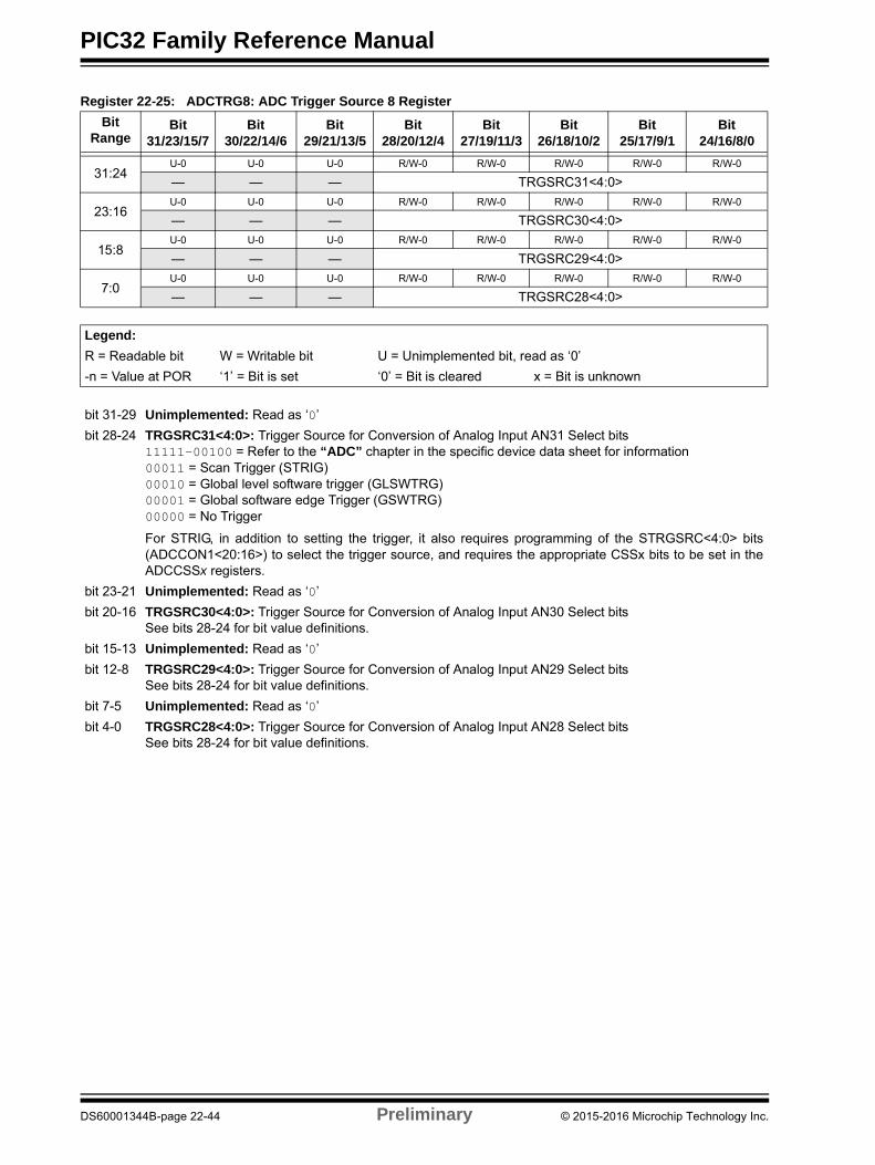
PIC32 Family Reference Manual
Register 22-25: ADCTRG8: ADC Trigger Source 8 Register
Bit Range
Bit31/23/15/7
Bit30/22/14/6
Bit29/21/13/5
Bit28/20/12/4
Bit27/19/11/3
Bit26/18/10/2
Bit25/17/9/1
Bit24/16/8/0
31:24U-0 U-0 U-0 R/W-0 R/W-0 R/W-0 R/W-0 R/W-0
— — — TRGSRC31<4:0>
23:16U-0 U-0 U-0 R/W-0 R/W-0 R/W-0 R/W-0 R/W-0
— — — TRGSRC30<4:0>
15:8U-0 U-0 U-0 R/W-0 R/W-0 R/W-0 R/W-0 R/W-0
— — — TRGSRC29<4:0>
7:0U-0 U-0 U-0 R/W-0 R/W-0 R/W-0 R/W-0 R/W-0
— — — TRGSRC28<4:0>
Legend:
R = Readable bit W = Writable bit U = Unimplemented bit, read as ‘0’
-n = Value at POR ‘1’ = Bit is set ‘0’ = Bit is cleared x = Bit is unknown
bit 31-29 Unimplemented: Read as ‘0’
bit 28-24 TRGSRC31<4:0>: Trigger Source for Conversion of Analog Input AN31 Select bits11111-00100 = Refer to the “ADC” chapter in the specific device data sheet for information00011 = Scan Trigger (STRIG)00010 = Global level software trigger (GLSWTRG)00001 = Global software edge Trigger (GSWTRG)00000 = No Trigger
For STRIG, in addition to setting the trigger, it also requires programming of the STRGSRC<4:0> bits(ADCCON1<20:16>) to select the trigger source, and requires the appropriate CSSx bits to be set in theADCCSSx registers.
bit 23-21 Unimplemented: Read as ‘0’
bit 20-16 TRGSRC30<4:0>: Trigger Source for Conversion of Analog Input AN30 Select bitsSee bits 28-24 for bit value definitions.
bit 15-13 Unimplemented: Read as ‘0’
bit 12-8 TRGSRC29<4:0>: Trigger Source for Conversion of Analog Input AN29 Select bitsSee bits 28-24 for bit value definitions.
bit 7-5 Unimplemented: Read as ‘0’
bit 4-0 TRGSRC28<4:0>: Trigger Source for Conversion of Analog Input AN28 Select bitsSee bits 28-24 for bit value definitions.
DS60001344B-page 22-44 Preliminary © 2015-2016 Microchip Technology Inc.
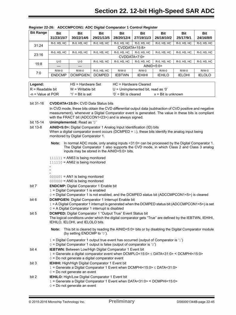
Section 22. 12-bit High-Speed SAR ADC
Register 22-26: ADCCMPCON1: ADC Digital Comparator 1 Control Register
Bit Range Bit31/23/15/7
Bit30/22/14/6
Bit29/21/13/5
Bit28/20/12/4
Bit27/19/11/3
Bit26/18/10/2
Bit25/17/9/1
Bit24/16/8/0
31:24R-0, HS, HC R-0, HS, HC R-0, HS, HC R-0, HS, HC R-0, HS, HC R-0, HS, HC R-0, HS, HC R-0, HS, HC
CVDDATA<15:8>
23:16R-0, HS, HC R-0, HS, HC R-0, HS, HC R-0, HS, HC R-0, HS, HC R-0, HS, HC R-0, HS, HC R-0, HS, HC
CVDDATA<7:0>
15:8U-0 U-0 R-0, HS, HC R-0, HS, HC R-0, HS, HC R-0, HS, HC R-0, HS, HC R-0, HS, HC
— — AINID<5:0>
7:0R/W-0 R/W-0 R-0, HS, HC R/W-0 R/W-0 R/W-0 R/W-0 R/W-0
ENDCMP DCMPGIEN DCMPED IEBTWN IEHIHI IEHILO IELOHI IELOLO
Legend: HS = Hardware Set HC = Hardware ClearedR = Readable bit W = Writable bit U = Unimplemented bit, read as ‘0’-n = Value at POR ‘1’ = Bit is set ‘0’ = Bit is cleared x = Bit is unknown
bit 31-16 CVDDATA<15:0>: CVD Data Status bits
In CVD mode, these bits obtain the CVD differential output data (subtraction of CVD positive and negativemeasurement), whenever a Digital Comparator event is generated. The value in these bits is compliantwith the FRACT bit (ADCCON1<23>) and is always signed.
bit 15-14 Unimplemented: Read as ‘0’
bit 13-8 AINID<5:0>: Digital Comparator 1 Analog Input Identification (ID) bitsWhen a digital comparator event occurs (DCMPED = 1), these bits identify the analog input being monitored by Digital Comparator 1.
Note: In normal ADC mode, only analog inputs <31:0> can be processed by the Digital Comparator 1.The Digital Comparator 1 also supports the CVD mode, in which Class 2 and Class 3 analoginputs may be stored in the AINID<5:0> bits.
111111 = AN63 is being monitored111110 = AN62 is being monitored•••000001 = AN1 is being monitored000000 = AN0 is being monitored
bit 7 ENDCMP: Digital Comparator 1 Enable bit1 = Digital Comparator 1 is enabled0 = Digital Comparator 1 is not enabled, and the DCMPED status bit (ADCCMPCON1<5>) is cleared
bit 6 DCMPGIEN: Digital Comparator 1 Interrupt Enable bit1 = A Digital Comparator 1 interrupt is generated when the DCMPED status bit (ADCCMPCON1<5>) is set0 = A Digital Comparator 1 interrupt is disabled
bit 5 DCMPED: Digital Comparator 1 “Output True” Event Status bitThe logical conditions under which the digital comparator gets “True” are defined by the IEBTWN, IEHIHI,IEHILO, IELOHI, and IELOLO bits.
Note: This bit is cleared by reading the AINID<5:0> bits or by disabling the Digital Comparator module(by setting ENDCMP to ‘0’).
1 = Digital Comparator 1 output true event has occurred (output of Comparator is ‘1’)0 = Digital Comparator 1 output is false (output of comparator is ‘0’)
bit 4 IEBTWN: Between Low/High Digital Comparator 1 Event bit1 = Generate a digital comparator event when DCMPLO<15:0> DATA<31:0> < DCMPHI<15:0>0 = Do not generate a digital comparator event
bit 3 IEHIHI: High/High Digital Comparator 1 Event bit1 = Generate a Digital Comparator 1 Event when DCMPHI<15:0> DATA<31:0>0 = Do not generate an event
bit 2 IEHILO: High/Low Digital Comparator 1 Event bit1 = Generate a Digital Comparator 1 Event when DATA<31:0> < DCMPHI<15:0>0 = Do not generate an event
© 2015-2016 Microchip Technology Inc. Preliminary DS60001344B-page 22-45
PIC32 Family Reference Manual
bit 1 IELOHI: Low/High Digital Comparator 1 Event bit1 = Generate a Digital Comparator 1 Event when DCMPLO<15:0> DATA<31:0>0 = Do not generate an event
bit 0 IELOLO: Low/Low Digital Comparator 1 Event bit1 = Generate a Digital Comparator 1 Event when DATA<31:0> < DCMPLO<15:0>0 = Do not generate an event
Register 22-26: ADCCMPCON1: ADC Digital Comparator 1 Control Register
DS60001344B-page 22-46 Preliminary © 2015-2016 Microchip Technology Inc.
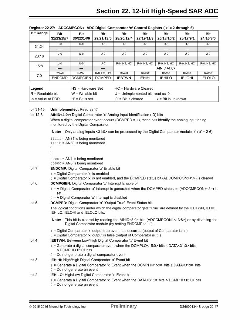
Section 22. 12-bit High-Speed SAR ADC
Register 22-27: ADCCMPCONx: ADC Digital Comparator ‘x’ Control Register (‘x’ = 2 through 6)
Bit Range Bit31/23/15/7
Bit30/22/14/6
Bit29/21/13/5
Bit28/20/12/4
Bit27/19/11/3
Bit26/18/10/2
Bit25/17/9/1
Bit24/16/8/0
31:24U-0 U-0 U-0 U-0 U-0 U-0 U-0 U-0
— — — — — — — —
23:16U-0 U-0 U-0 U-0 U-0 U-0 U-0 U-0
— — — — — — — —
15:8U-0 U-0 U-0 R-0, HS, HC R-0, HS, HC R-0, HS, HC R-0, HS, HC R-0, HS, HC
— — — AINID<4:0>
7:0R/W-0 R/W-0 R-0, HS, HC R/W-0 R/W-0 R/W-0 R/W-0 R/W-0
ENDCMP DCMPGIEN DCMPED IEBTWN IEHIHI IEHILO IELOHI IELOLO
Legend: HS = Hardware Set HC = Hardware Cleared
R = Readable bit W = Writable bit U = Unimplemented bit, read as ‘0’
-n = Value at POR ‘1’ = Bit is set ‘0’ = Bit is cleared x = Bit is unknown
bit 31-13 Unimplemented: Read as ‘0’
bit 12-8 AINID<4:0>: Digital Comparator ‘x’ Analog Input Identification (ID) bits
When a digital comparator event occurs (DCMPED = 1), these bits identify the analog input being monitored by the Digital Comparator.
Note: Only analog inputs <31:0> can be processed by the Digital Comparator module ‘x’ (‘x’ = 2-6).
11111 = AN31 is being monitored11110 = AN30 is being monitored•••
00001 = AN1 is being monitored00000 = AN0 is being monitored
bit 7 ENDCMP: Digital Comparator ‘x’ Enable bit
1 = Digital Comparator ‘x’ is enabled0 = Digital Comparator ‘x’ is not enabled, and the DCMPED status bit (ADCCMPCONx<5>) is cleared
bit 6 DCMPGIEN: Digital Comparator ‘x’ Interrupt Enable bit
1 = A Digital Comparator ‘x’ interrupt is generated when the DCMPED status bit (ADCCMPCONx<5>) isset
0 = A Digital Comparator ‘x’ interrupt is disabled
bit 5 DCMPED: Digital Comparator ‘x’ “Output True” Event Status bit
The logical conditions under which the digital comparator gets “True” are defined by the IEBTWN, IEHIHI,IEHILO, IELOHI and IELOLO bits.
Note: This bit is cleared by reading the AINID<5:0> bits (ADCCMPCON1<13:8>) or by disabling theDigital Comparator module (by setting ENDCMP to ‘0’).
1 = Digital Comparator ‘x’ output true event has occurred (output of Comparator is ‘1’)0 = Digital Comparator ‘x’ output is false (output of Comparator is ‘0’)
bit 4 IEBTWN: Between Low/High Digital Comparator ‘x’ Event bit
1 = Generate a digital comparator event when the DCMPLO<15:0> bits DATA<31:0> bits< DCMPHI<15:0> bits
0 = Do not generate a digital comparator event
bit 3 IEHIHI: High/High Digital Comparator ‘x’ Event bit
1 = Generate a Digital Comparator ‘x’ Event when the DCMPHI<15:0> bits DATA<31:0> bits0 = Do not generate an event
bit 2 IEHILO: High/Low Digital Comparator ‘x’ Event bit
1 = Generate a Digital Comparator ‘x’ Event when the DATA<31:0> bits < DCMPHI<15:0> bits0 = Do not generate an event
© 2015-2016 Microchip Technology Inc. Preliminary DS60001344B-page 22-47
PIC32 Family Reference Manual
bit 1 IELOHI: Low/High Digital Comparator ‘x’ Event bit
1 = Generate a Digital Comparator ‘x’ Event when the DCMPLO<15:0> bits DATA<31:0> bits0 = Do not generate an event
bit 0 IELOLO: Low/Low Digital Comparator ‘x’ Event bit
1 = Generate a Digital Comparator ‘x’ Event when the DATA<31:0> bits < DCMPLO<15:0> bits0 = Do not generate an event
Register 22-27: ADCCMPCONx: ADC Digital Comparator ‘x’ Control Register (‘x’ = 2 through 6) (Continued)
DS60001344B-page 22-48 Preliminary © 2015-2016 Microchip Technology Inc.

Section 22. 12-bit High-Speed SAR ADC
Register 22-28: ADCFSTAT: ADC FIFO Status Register
Bit Range Bit31/23/15/7
Bit30/22/14/6
Bit29/21/13/5
Bit28/20/12/4
Bit27/19/11/3
Bit26/18/10/2
Bit25/17/9/1
Bit24/16/8/0
31:24R/W-0 R/W-0 R/W-0 R/W-0 R/W-0 R/W-0 R/W-0 R/W-0
FEN ADC6EN ADC5EN ADC4EN ADC3EN ADC2EN ADC1EN ADC0EN
23:16R/W-0 R-0, HS, HC R-0, HS, HC U-0 U-0 U-0 U-0 U-0
FIEN FRDY FWROVERR — — — — —
15:8R-0 R-0 R-0 R-0 R-0 R-0 R-0 R-0
FCNT<7:0>
7:0R-0 U-0 U-0 U-0 U-0 R-0 R-0 R-0
FSIGN — — — — ADCID<2:0>
Legend:
R = Readable bit W = Writable bit U = Unimplemented bit, read as ‘0’
-n = Value at POR ‘1’ = Bit is set ‘0’ = Bit is cleared x = Bit is unknown
bit 31 FEN: FIFO Enable bit
1 = FIFO is enabled0 = FIFO is disabled; no data is being saved into the FIFO
bit 30-24 ADC6EN:ADC0EN: ADC6-ADC0 Enable bits
1 = Converted output data of ADC6-ADC0 is stored in the FIFO0 = Converted output data of ADC6-ADC0 is not stored in the FIFO
Note: While using FIFO, the output data is additionally stored in the respective output data register(ADCDATAx).
bit 23 FIEN: FIFO Interrupt Enable bit
1 = FIFO interrupts are enabled; an interrupt is generated once the FRDY bit is set0 = FIFO interrupts are disabled
bit 22 FRDY: FIFO Data Ready Interrupt Status bit
1 = FIFO has data to be read0 = No data is available in the FIFO
Note: This bit is cleared when the FIFO output data in ADCFIFO has been read and there is noadditional data ready in the FIFO (that is, the FIFO is empty).
bit 21 FWROVERR: FIFO Write Overflow Error Status bit
1 = A write overflow error in the FIFO has occurred (circular FIFO)0 = A write overflow error in the FIFO has not occurred
Note: This bit is cleared after ADCFSTAT<23:16> are read by software.
bit 15-8 FCNT<7:0>: FIFO Data Entry Count Status bit
The value in these bits indicates the number of data entries in the FIFO.
bit 7 FSIGN: FIFO Sign Setting bit
This bit reflects the sign of data stored in the ADCFIFO register.
bit 6-3 Unimplemented: Read as ‘0’
bit 2-0 ADCID<2:0>: ADC6-ADC0 Identifier bits
These bits specify the ADC module whose data is stored in the FIFO.
111 = Reserved110 = Converted data of ADC6 is stored in FIFO•••
000 = Converted data of ADC0 is stored in FIFO
© 2015-2016 Microchip Technology Inc. Preliminary DS60001344B-page 22-49
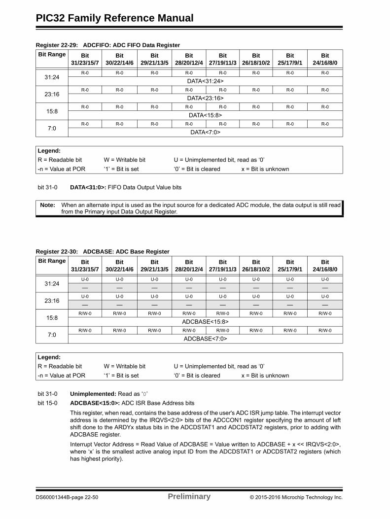
PIC32 Family Reference Manual
Register 22-29: ADCFIFO: ADC FIFO Data Register
Bit Range Bit31/23/15/7
Bit30/22/14/6
Bit29/21/13/5
Bit28/20/12/4
Bit27/19/11/3
Bit26/18/10/2
Bit25/17/9/1
Bit24/16/8/0
31:24R-0 R-0 R-0 R-0 R-0 R-0 R-0 R-0
DATA<31:24>
23:16R-0 R-0 R-0 R-0 R-0 R-0 R-0 R-0
DATA<23:16>
15:8R-0 R-0 R-0 R-0 R-0 R-0 R-0 R-0
DATA<15:8>
7:0R-0 R-0 R-0 R-0 R-0 R-0 R-0 R-0
DATA<7:0>
Legend:
R = Readable bit W = Writable bit U = Unimplemented bit, read as ‘0’
-n = Value at POR ‘1’ = Bit is set ‘0’ = Bit is cleared x = Bit is unknown
bit 31-0 DATA<31:0>: FIFO Data Output Value bits
Note: When an alternate input is used as the input source for a dedicated ADC module, the data output is still readfrom the Primary input Data Output Register.
Register 22-30: ADCBASE: ADC Base Register
Bit Range Bit31/23/15/7
Bit30/22/14/6
Bit29/21/13/5
Bit28/20/12/4
Bit27/19/11/3
Bit26/18/10/2
Bit25/17/9/1
Bit24/16/8/0
31:24U-0 U-0 U-0 U-0 U-0 U-0 U-0 U-0
— — — — — — — —
23:16U-0 U-0 U-0 U-0 U-0 U-0 U-0 U-0
— — — — — — — —
15:8R/W-0 R/W-0 R/W-0 R/W-0 R/W-0 R/W-0 R/W-0 R/W-0
ADCBASE<15:8>
7:0R/W-0 R/W-0 R/W-0 R/W-0 R/W-0 R/W-0 R/W-0 R/W-0
ADCBASE<7:0>
Legend:
R = Readable bit W = Writable bit U = Unimplemented bit, read as ‘0’
-n = Value at POR ‘1’ = Bit is set ‘0’ = Bit is cleared x = Bit is unknown
bit 31-0 Unimplemented: Read as ‘0’
bit 15-0 ADCBASE<15:0>: ADC ISR Base Address bits
This register, when read, contains the base address of the user's ADC ISR jump table. The interrupt vectoraddress is determined by the IRQVS<2:0> bits of the ADCCON1 register specifying the amount of leftshift done to the ARDYx status bits in the ADCDSTAT1 and ADCDSTAT2 registers, prior to adding withADCBASE register.
Interrupt Vector Address = Read Value of ADCBASE = Value written to ADCBASE + x << IRQVS<2:0>,where ‘x’ is the smallest active analog input ID from the ADCDSTAT1 or ADCDSTAT2 registers (whichhas highest priority).
DS60001344B-page 22-50 Preliminary © 2015-2016 Microchip Technology Inc.

Section 22. 12-bit High-Speed SAR ADC
Register 22-31: ADCDATAx: ADC Output Data Register (‘x’ = 0 through 63)
Bit Range Bit31/23/15/7
Bit30/22/14/6
Bit29/21/13/5
Bit28/20/12/4
Bit27/19/11/3
Bit26/18/10/2
Bit25/17/9/1
Bit24/16/8/0
31:24R-0 R-0 R-0 R-0 R-0 R-0 R-0 R-0
DATA<31:24>
23:16R-0 R-0 R-0 R-0 R-0 R-0 R-0 R-0
DATA<23:16>
15:8R-0 R-0 R-0 R-0 R-0 R-0 R-0 R-0
DATA<15:8>
7:0R-0 R-0 R-0 R-0 R-0 R-0 R-0 R-0
DATA<7:0>
Legend:
R = Readable bit W = Writable bit U = Unimplemented bit, read as ‘0’
-n = Value at POR ‘1’ = Bit is set ‘0’ = Bit is cleared x = Bit is unknown
bit 31-0 DATA<31:0>: ADC Converted Data Output bits.
Note 1: When an alternate input is used as the input source for a dedicated ADC module, the data output is still read from the Primary input Data Output Register.
2: Reading the ADCDATAx register value after changing the FRACT bit converts the data into the format specified by FRACT bit.
© 2015-2016 Microchip Technology Inc. Preliminary DS60001344B-page 22-51

PIC32 Family Reference Manual
Register 22-32: ADCDMASTAT: ADC DMA Status Register
Bit Range
Bit31/23/15/7
Bit30/22/14/6
Bit29/21/13/5
Bit28/20/12/4
Bit27/19/11/3
Bit26/18/10/2
Bit25/17/9/1
Bit24/16/8/0
31:24R/W-0 R/W-0 R/W-0 R/W-0 R/W-0 R/W-0 R/W-0 R/W-0
DMAGEN RBFIEN6 RBFIEN5 RBFIEN4 RBFIEN3 RBFIEN2 RBFIEN1 RBFIEN0
23:16R-0, HS, HC R-0, HS, HC R-0, HS, HC R-0, HS, HC R-0, HS, HC R-0, HS, HC R-0, HS, HC R-0, HS, HC
DMAWROVERR RBF6 RBF5 RBF4 RBF3 RBF2 RBF1 RBF0
15:8R/W-0 R/W-0 R/W-0 R/W-0 R/W-0 R/W-0 R/W-0 R/W-0
DMACNTEN RAFIEN6 RAFIEN5 RAFIEN4 RAFIEN3 RAFIEN2 RAFIEN1 RAFIEN0
7:0U-0 R-0, HS, HC R-0, HS, HC R-0, HS, HC R-0, HS, HC R-0, HS, HC R-0, HS, HC R-0, HS, HC
— RAF6 RAF5 RAF4 RAF3 RAF2 RAF1 RAF0
Legend:
R = Readable bit W = Writable bit U = Unimplemented bit, read as ‘0’
-n = Value at POR ‘1’ = Bit is set ‘0’ = Bit is cleared x = Bit is unknown
bit 31 DMAGEN: DMA Global Enable bit
1 = DMA engine is enabled globally for all ADC modules. To use DMA, individual dedicated ADC modulesshould enable their DMAEN bits (ADCxTIME<23>).
0 = DMA engine is globally disabled for all ADC modules
bit 30-24 RBFIEN6:RBFIEN0: RAM Buffer B Full Interrupt Enable bit
1 = Interrupts are enabled and generated when the RBFx Status bit is set0 = Interrupts are disabled
bit 23 DMAWROVERR: DMA Write Overflow Error bit
1 = DMA write overflow error has occurred (circular buffer)0 = DMA write overflow error has not occurred
Note: This bit is cleared by hardware after a software read of the ADCDMASTAT register.
bit 22-16 RBF6:RBF0: RAM Buffer B Full Status bit
1 = RAM Buffer B is full0 = RAM Buffer B is not full
Note: These bits are self-clearing upon being a read by software.
bit 15 DMACNTEN: DMA Buffer Sample Count Enable bit
The DMA engine will save the current sample count for each buffer in the table starting at the ADCCNTBaddress after each sample write into the corresponding buffer in the SRAM.
bit 14-8 RAFIEN6:RAFIEN0: RAM Buffer A Full Interrupt Enable bit
1 = Interrupts are enabled and generated when the RAFx status bit is set0 = Interrupts are disabled
bit 7 Unimplemented: Read as ‘0’
bit 6-0 RAF6:RAF0: RAM Buffer A Full Status bit
1 = RAM Buffer A is full0 = RAM Buffer A is not full
Note: These bits are self-clearing upon being a read by software.
DS60001344B-page 22-52 Preliminary © 2015-2016 Microchip Technology Inc.

Section 22. 12-bit High-Speed SAR ADC
Register 22-33: ADCCNTB: ADC Sample Count Base Address Register
Bit Range Bit31/23/15/7
Bit30/22/14/6
Bit29/21/13/5
Bit28/20/12/4
Bit27/19/11/3
Bit26/18/10/2
Bit25/17/9/1
Bit24/16/8/0
31:24R/W-0 R/W-0 R/W-0 R/W-0 R/W-0 R/W-0 R/W-0 R/W-0
CNTBADDR<31:24>
23:16R/W-0 R/W-0 R/W-0 R/W-0 R/W-0 R/W-0 R/W-0 R/W-0
CNTBADDR<23:16>
15:8R/W-0 R/W-0 R/W-0 R/W-0 R/W-0 R/W-0 R/W-0 R/W-0
CNTBADDR<15:8>
7:0R/W-0 R/W-0 R/W-0 R/W-0 R/W-0 R/W-0 R/W-0 R/W-0
CNTBADDR<7:0>
Legend:
R = Readable bit W = Writable bit U = Unimplemented bit, read as ‘0’
-n = Value at POR ‘1’ = Bit is set ‘0’ = Bit is cleared x = Bit is unknown
bit 31 CNTBADDR<31:0>: Analog-to-Digital Count Base Address bits
The ADCCNTB register contains the user-defined RAM address at which the DMA engine will start savingthe current count of output samples (if the DMACNTEN bit (ADCDMASTAT<15>) is set), which is alreadywritten to each of the buffers in the System RAM for each ADC module. The ADCx module will have itsBuffer A current sample count saved at the address ((ADCCNTB) + 2 * x) and its Buffer B current samplecount saved at the address ((ADCCNTB) + (2 * x + 1)). Where 'x' is the dedicated ADC module ID.
Register 22-34: ADCDMAB: ADC DMA Base Address Register
Bit Range Bit31/23/15/7
Bit30/22/14/6
Bit29/21/13/5
Bit28/20/12/4
Bit27/19/11/3
Bit26/18/10/2
Bit25/17/9/1
Bit24/16/8/0
31:24R/W-0 R/W-0 R/W-0 R/W-0 R/W-0 R/W-0 R/W-0 R/W-0
DMABADDR<31:24>
23:16R/W-0 R/W-0 R/W-0 R/W-0 R/W-0 R/W-0 R/W-0 R/W-0
DMABADDR<23:16>
15:8R/W-0 R/W-0 R/W-0 R/W-0 R/W-0 R/W-0 R/W-0 R/W-0
DMABADDR<15:8>
7:0R/W-0 R/W-0 R/W-0 R/W-0 R/W-0 R/W-0 R/W-0 R/W-0
DMABADDR<7:0>
Legend:
R = Readable bit W = Writable bit U = Unimplemented bit, read as ‘0’
-n = Value at POR ‘1’ = Bit is set ‘0’ = Bit is cleared x = Bit is unknown
bit 31 DMABADDR<31:0>: DMA Base Address bits
The ADCDMAB register contains the user-specified RAM address at which DMA engine will start savingthe converted data. The address of saving each data is specified by the following relations:
Buffer A starting address at: ADCDMAB + (2 * x) * 2(ADCON1bits.DMABL + 1)
Buffer B starting at: ADCDMAB + (2 * (x + 1)) * 2(ADCON1bits.DMABL + 1)
Where, 'x' is the dedicated ADC module ID.
© 2015-2016 Microchip Technology Inc. Preliminary DS60001344B-page 22-53
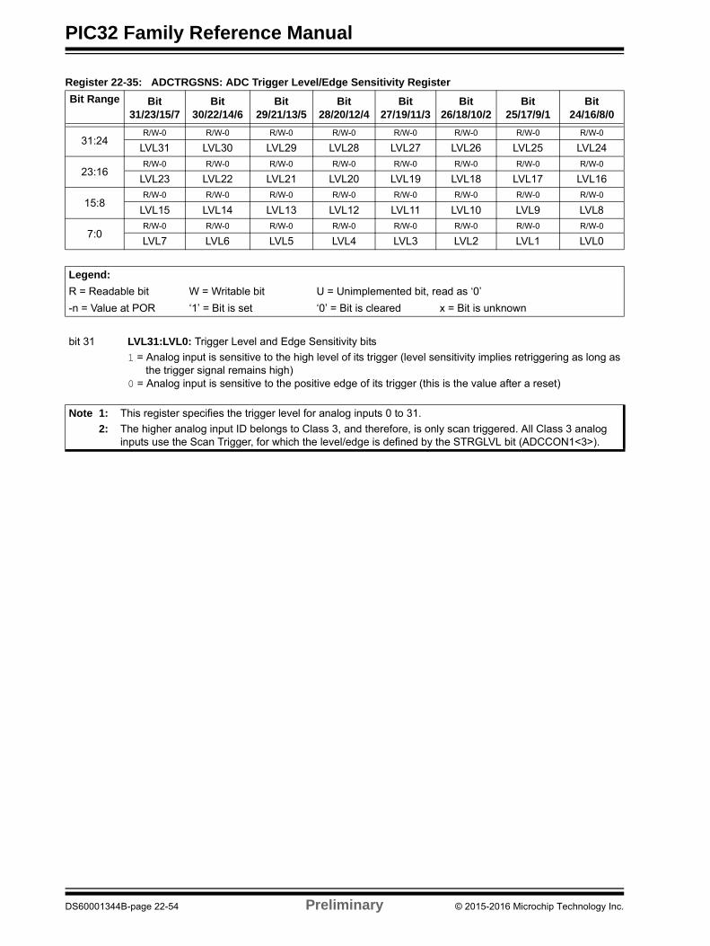
PIC32 Family Reference Manual
Register 22-35: ADCTRGSNS: ADC Trigger Level/Edge Sensitivity Register
Bit Range Bit31/23/15/7
Bit30/22/14/6
Bit29/21/13/5
Bit28/20/12/4
Bit27/19/11/3
Bit26/18/10/2
Bit25/17/9/1
Bit24/16/8/0
31:24R/W-0 R/W-0 R/W-0 R/W-0 R/W-0 R/W-0 R/W-0 R/W-0
LVL31 LVL30 LVL29 LVL28 LVL27 LVL26 LVL25 LVL24
23:16R/W-0 R/W-0 R/W-0 R/W-0 R/W-0 R/W-0 R/W-0 R/W-0
LVL23 LVL22 LVL21 LVL20 LVL19 LVL18 LVL17 LVL16
15:8R/W-0 R/W-0 R/W-0 R/W-0 R/W-0 R/W-0 R/W-0 R/W-0
LVL15 LVL14 LVL13 LVL12 LVL11 LVL10 LVL9 LVL8
7:0R/W-0 R/W-0 R/W-0 R/W-0 R/W-0 R/W-0 R/W-0 R/W-0
LVL7 LVL6 LVL5 LVL4 LVL3 LVL2 LVL1 LVL0
Legend:
R = Readable bit W = Writable bit U = Unimplemented bit, read as ‘0’
-n = Value at POR ‘1’ = Bit is set ‘0’ = Bit is cleared x = Bit is unknown
bit 31 LVL31:LVL0: Trigger Level and Edge Sensitivity bits
1 = Analog input is sensitive to the high level of its trigger (level sensitivity implies retriggering as long asthe trigger signal remains high)
0 = Analog input is sensitive to the positive edge of its trigger (this is the value after a reset)
Note 1: This register specifies the trigger level for analog inputs 0 to 31.
2: The higher analog input ID belongs to Class 3, and therefore, is only scan triggered. All Class 3 analog inputs use the Scan Trigger, for which the level/edge is defined by the STRGLVL bit (ADCCON1<3>).
DS60001344B-page 22-54 Preliminary © 2015-2016 Microchip Technology Inc.
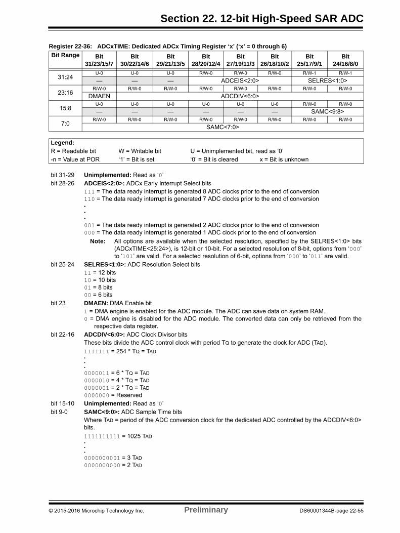
Section 22. 12-bit High-Speed SAR ADC
Register 22-36: ADCxTIME: Dedicated ADCx Timing Register ‘x’ (‘x’ = 0 through 6)
Bit Range Bit31/23/15/7
Bit30/22/14/6
Bit29/21/13/5
Bit28/20/12/4
Bit27/19/11/3
Bit26/18/10/2
Bit25/17/9/1
Bit24/16/8/0
31:24U-0 U-0 U-0 R/W-0 R/W-0 R/W-0 R/W-1 R/W-1
— — — ADCEIS<2:0> SELRES<1:0>
23:16R/W-0 R/W-0 R/W-0 R/W-0 R/W-0 R/W-0 R/W-0 R/W-0
DMAEN ADCDIV<6:0>
15:8U-0 U-0 U-0 U-0 U-0 U-0 R/W-0 R/W-0
— — — — — — SAMC<9:8>
7:0R/W-0 R/W-0 R/W-0 R/W-0 R/W-0 R/W-0 R/W-0 R/W-0
SAMC<7:0>
Legend:R = Readable bit W = Writable bit U = Unimplemented bit, read as ‘0’-n = Value at POR ‘1’ = Bit is set ‘0’ = Bit is cleared x = Bit is unknown
bit 31-29 Unimplemented: Read as ‘0’bit 28-26 ADCEIS<2:0>: ADCx Early Interrupt Select bits
111 = The data ready interrupt is generated 8 ADC clocks prior to the end of conversion110 = The data ready interrupt is generated 7 ADC clocks prior to the end of conversion•••
001 = The data ready interrupt is generated 2 ADC clocks prior to the end of conversion000 = The data ready interrupt is generated 1 ADC clock prior to the end of conversion
Note: All options are available when the selected resolution, specified by the SELRES<1:0> bits(ADCxTIME<25:24>), is 12-bit or 10-bit. For a selected resolution of 8-bit, options from ‘000’to ‘101’ are valid. For a selected resolution of 6-bit, options from ‘000’ to ‘011’ are valid.
bit 25-24 SELRES<1:0>: ADC Resolution Select bits11 = 12 bits10 = 10 bits01 = 8 bits00 = 6 bits
bit 23 DMAEN: DMA Enable bit1 = DMA engine is enabled for the ADC module. The ADC can save data on system RAM.0 = DMA engine is disabled for the ADC module. The converted data can only be retrieved from the
respective data register.bit 22-16 ADCDIV<6:0>: ADC Clock Divisor bits
These bits divide the ADC control clock with period TQ to generate the clock for ADC (TAD).
1111111 = 254 * TQ = TAD•••
0000011 = 6 * TQ = TAD
0000010 = 4 * TQ = TAD
0000001 = 2 * TQ = TAD
0000000 = Reservedbit 15-10 Unimplemented: Read as ‘0’bit 9-0 SAMC<9:0>: ADC Sample Time bits
Where TAD = period of the ADC conversion clock for the dedicated ADC controlled by the ADCDIV<6:0>bits.
1111111111 = 1025 TAD•••
0000000001 = 3 TAD
0000000000 = 2 TAD
© 2015-2016 Microchip Technology Inc. Preliminary DS60001344B-page 22-55

PIC32 Family Reference Manual
Register 22-37: ADCEIEN1: ADC Early Interrupt Enable Register 1
Bit Range
Bit31/23/15/7
Bit30/22/14/6
Bit29/21/13/5
Bit28/20/12/4
Bit27/19/11/3
Bit26/18/10/2
Bit25/17/9/1
Bit24/16/8/0
31:24R/W-0 R/W-0 R/W-0 R/W-0 R/W-0 R/W-0 R/W-0 R/W-0
EIEN31 EIEN30 EIEN29 EIEN28 EIEN27 EIEN26 EIEN25 EIEN24
23:16R/W-0 R/W-0 R/W-0 R/W-0 R/W-0 R/W-0 R/W-0 R/W-0
EIEN23 EIEN22 EIEN21 EIEN20 EIEN19 EIEN18 EIEN17 EIEN16
15:8R/W-0 R/W-0 R/W-0 R/W-0 R/W-0 R/W-0 R/W-0 R/W-0
EIEN15 EIEN14 EIEN13 EIEN12 EIEN11 EIEN10 EIEN9 EIEN8
7:0R/W-0 R/W-0 R/W-0 R/W-0 R/W-0 R/W-0 R/W-0 R/W-0
EIEN7 EIEN6 EIEN5 EIEN4 EIEN3 EIEN2 EIEN1 EIEN0
Legend:
R = Readable bit W = Writable bit U = Unimplemented bit, read as ‘0’
-n = Value at POR ‘1’ = Bit is set ‘0’ = Bit is cleared x = Bit is unknown
bit 31-0 EIEN31:EIEN0: Early Interrupt Enable for Analog Input bits
1 = Early Interrupts are enabled for the selected analog input. The interrupt is generated after the earlyinterrupt event occurs (indicated by the EIRDYx bit ('x' = 31-0) of the ADCEISTAT1 register)
0 = Interrupts are disabled
Register 22-38: ADCEIEN2: ADC Early Interrupt Enable Register 2
Bit Range
Bit31/23/15/7
Bit30/22/14/6
Bit29/21/13/5
Bit28/20/12/4
Bit27/19/11/3
Bit26/18/10/2
Bit25/17/9/1
Bit24/16/8/0
31:24R/W-0 R/W-0 R/W-0 R/W-0 R/W-0 R/W-0 R/W-0 R/W-0
EIEN63 EIEN62 EIEN61 EIEN60 EIEN59 EIEN58 EIEN57 EIEN56
23:16R/W-0 R/W-0 R/W-0 R/W-0 R/W-0 R/W-0 R/W-0 R/W-0
EIEN55 EIEN54 EIEN53 EIEN52 EIEN51 EIEN50 EIEN49 EIEN48
15:8R/W-0 R/W-0 R/W-0 R/W-0 R/W-0 R/W-0 R/W-0 R/W-0
EIEN47 EIEN46 EIEN45 EIEN44 EIEN43 EIEN42 EIEN41 EIEN40
7:0R/W-0 R/W-0 R/W-0 R/W-0 R/W-0 R/W-0 R/W-0 R/W-0
EIEN39 EIEN38 EIEN37 EIEN36 EIEN35 EIEN34 EIEN33 EIEN32
Legend:
R = Readable bit W = Writable bit U = Unimplemented bit, read as ‘0’
-n = Value at POR ‘1’ = Bit is set ‘0’ = Bit is cleared x = Bit is unknown
bit 31-0 EIEN63:EIEN32: Early Interrupt Enable for Analog Input bits
1 = Early Interrupts are enabled for the selected analog input. The interrupt is generated after the earlyinterrupt event occurs (indicated by the EIRDYx bit ('x' = 63-32) of the ADCEISTAT2 register)
0 = Interrupts are disabled
DS60001344B-page 22-56 Preliminary © 2015-2016 Microchip Technology Inc.

Section 22. 12-bit High-Speed SAR ADC
Register 22-39: ADCEISTAT1: ADC Early Interrupt Status Register 1
Bit Range
Bit31/23/15/7
Bit30/22/14/6
Bit29/21/13/5
Bit28/20/12/4
Bit27/19/11/3
Bit26/18/10/2
Bit25/17/9/1
Bit24/16/8/0
31:24R-0, HS, HC R-0, HS, HC R-0, HS, HC R-0, HS, HC R-0, HS, HC R-0, HS, HC R-0, HS, HC R-0, HS, HC
EIRDY31 EIRDY30 EIRDY29 EIRDY28 EIRDY27 EIRDY26 EIRDY25 EIRDY24
23:16R-0, HS, HC R-0, HS, HC R-0, HS, HC R-0, HS, HC R-0, HS, HC R-0, HS, HC R-0, HS, HC R-0, HS, HC
EIRDY23 EIRDY22 EIRDY21 EIRDY20 EIRDY19 EIRDY18 EIRDY17 EIRDY16
15:8R-0, HS, HC R-0, HS, HC R-0, HS, HC R-0, HS, HC R-0, HS, HC R-0, HS, HC R-0, HS, HC R-0, HS, HC
EIRDY15 EIRDY14 EIRDY13 EIRDY12 EIRDY11 EIRDY10 EIRDY9 EIRDY8
7:0R-0, HS, HC R-0, HS, HC R-0, HS, HC R-0, HS, HC R-0, HS, HC R-0, HS, HC R-0, HS, HC R-0, HS, HC
EIRDY7 EIRDY6 EIRDY5 EIRDY4 EIRDY3 EIRDY2 EIRDY1 EIRDY0
Legend: HS = Hardware Set HC = Hardware Cleared
R = Readable bit W = Writable bit U = Unimplemented bit, read as ‘0’
-n = Value at POR ‘1’ = Bit is set ‘0’ = Bit is cleared x = Bit is unknown
bit 31-0 EIRDY31:EIRDY0: Early Interrupt for Corresponding Analog Input Ready bits
1 = This bit is set when the early interrupt event occurs for the specified analog input. An interrupt will begenerated if early interrupts are enabled in the ADCEIEN1 register. For the Class 1 analog inputs, thisbit will set as per the configuration of the ADCEIS<2:0> bits in the ADCxTIME register. For the sharedADC module, this bit will be set as per the configuration of the ADCEIS<2:0> bits in the ADCCON2register.
0 = Interrupts are disabled
Register 22-40: ADCEISTAT2: ADC Early Interrupt Status Register 2
Bit Range
Bit31/23/15/7
Bit30/22/14/6
Bit29/21/13/5
Bit28/20/12/4
Bit27/19/11/3
Bit26/18/10/2
Bit25/17/9/1
Bit24/16/8/0
31:24R-0, HS, HC R-0, HS, HC R-0, HS, HC R-0, HS, HC R-0, HS, HC R-0, HS, HC R-0, HS, HC R-0, HS, HC
EIRDY63 EIRDY62 EIRDY61 EIRDY60 EIRDY59 EIRDY58 EIRDY57 EIRDY56
23:16R-0, HS, HC R-0, HS, HC R-0, HS, HC R-0, HS, HC R-0, HS, HC R-0, HS, HC R-0, HS, HC R-0, HS, HC
EIRDY55 EIRDY54 EIRDY53 EIRDY52 EIRDY51 EIRDY50 EIRDY49 EIRDY48
15:8R-0, HS, HC R-0, HS, HC R-0, HS, HC R-0, HS, HC R-0, HS, HC R-0, HS, HC R-0, HS, HC R-0, HS, HC
EIRDY47 EIRDY46 EIRDY45 EIRDY44 EIRDY43 EIRDY42 EIRDY41 EIRDY40
7:0R-0, HS, HC R-0, HS, HC R-0, HS, HC R-0, HS, HC R-0, HS, HC R-0, HS, HC R-0, HS, HC R-0, HS, HC
EIRDY39 EIRDY38 EIRDY37 EIRDY36 EIRDY35 EIRDY34 EIRDY33 EIRDY32
Legend: HS = Hardware Set HC = Hardware Cleared
R = Readable bit W = Writable bit U = Unimplemented bit, read as ‘0’
-n = Value at POR ‘1’ = Bit is set ‘0’ = Bit is cleared x = Bit is unknown
bit 31-0 EIRDY63:EIRDY32: Early Interrupt for Corresponding Analog Input Ready bits
1 = This bit is set when the early interrupt event occurs for the specified analog input. An interrupt will begenerated if early interrupts are enabled in the ADCEIEN2 register. For the Class 1 analog inputs, thisbit will set as per the configuration of the ADCEIS<2:0> bits in the ADCxTIME register. For the sharedADC module, this bit will be set as per the configuration of the ADCEIS<2:0> bits in the ADCCON2register.
0 = Interrupts are disabled
© 2015-2016 Microchip Technology Inc. Preliminary DS60001344B-page 22-57
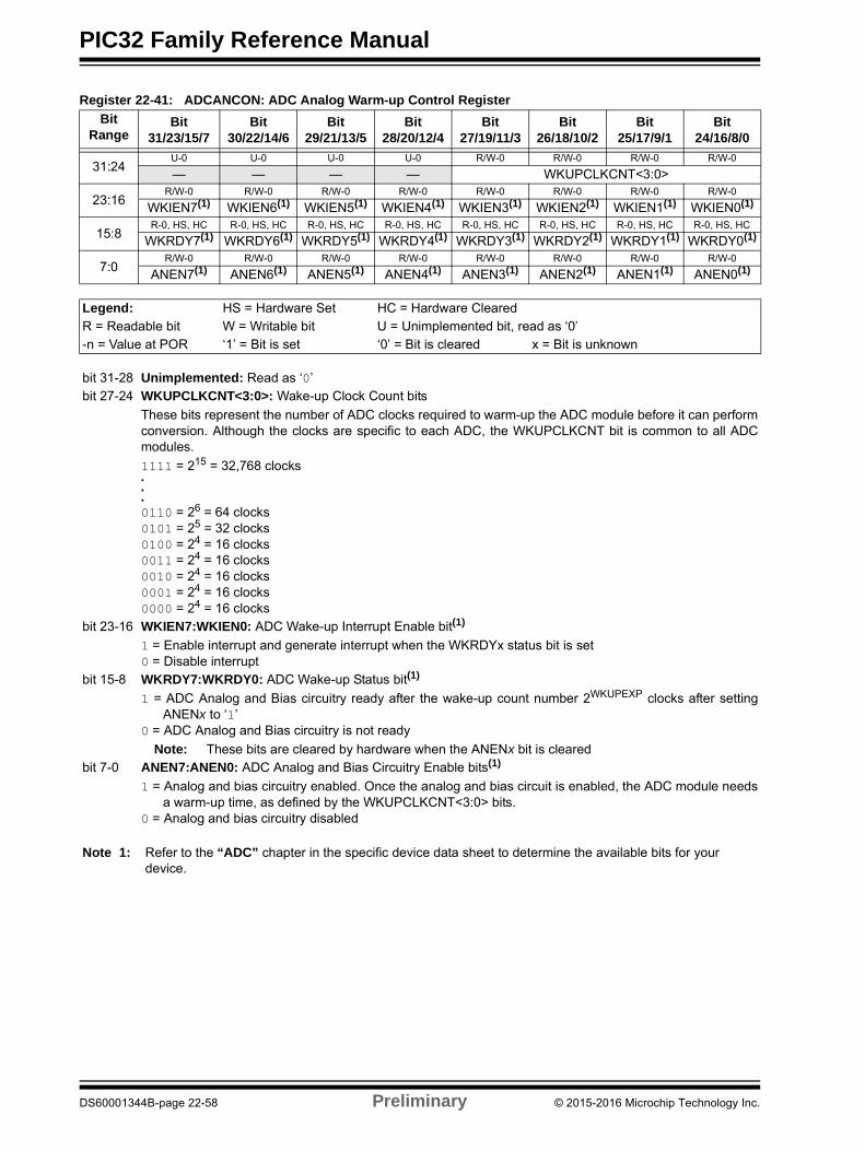
PIC32 Family Reference Manual
Register 22-41: ADCANCON: ADC Analog Warm-up Control Register
Bit Range
Bit31/23/15/7
Bit30/22/14/6
Bit29/21/13/5
Bit28/20/12/4
Bit27/19/11/3
Bit26/18/10/2
Bit25/17/9/1
Bit24/16/8/0
31:24U-0 U-0 U-0 U-0 R/W-0 R/W-0 R/W-0 R/W-0
— — — — WKUPCLKCNT<3:0>
23:16R/W-0 R/W-0 R/W-0 R/W-0 R/W-0 R/W-0 R/W-0 R/W-0
WKIEN7(1) WKIEN6(1) WKIEN5(1) WKIEN4(1) WKIEN3(1) WKIEN2(1) WKIEN1(1) WKIEN0(1)
15:8R-0, HS, HC R-0, HS, HC R-0, HS, HC R-0, HS, HC R-0, HS, HC R-0, HS, HC R-0, HS, HC R-0, HS, HC
WKRDY7(1) WKRDY6(1) WKRDY5(1) WKRDY4(1) WKRDY3(1) WKRDY2(1) WKRDY1(1) WKRDY0(1)
7:0R/W-0 R/W-0 R/W-0 R/W-0 R/W-0 R/W-0 R/W-0 R/W-0
ANEN7(1) ANEN6(1) ANEN5(1) ANEN4(1) ANEN3(1) ANEN2(1) ANEN1(1) ANEN0(1)
Legend: HS = Hardware Set HC = Hardware ClearedR = Readable bit W = Writable bit U = Unimplemented bit, read as ‘0’-n = Value at POR ‘1’ = Bit is set ‘0’ = Bit is cleared x = Bit is unknown
bit 31-28 Unimplemented: Read as ‘0’bit 27-24 WKUPCLKCNT<3:0>: Wake-up Clock Count bits
These bits represent the number of ADC clocks required to warm-up the ADC module before it can performconversion. Although the clocks are specific to each ADC, the WKUPCLKCNT bit is common to all ADCmodules.
1111 = 215 = 32,768 clocks•••
0110 = 26 = 64 clocks0101 = 25 = 32 clocks0100 = 24 = 16 clocks0011 = 24 = 16 clocks0010 = 24 = 16 clocks0001 = 24 = 16 clocks0000 = 24 = 16 clocks
bit 23-16 WKIEN7:WKIEN0: ADC Wake-up Interrupt Enable bit(1)
1 = Enable interrupt and generate interrupt when the WKRDYx status bit is set0 = Disable interrupt
bit 15-8 WKRDY7:WKRDY0: ADC Wake-up Status bit(1)
1 = ADC Analog and Bias circuitry ready after the wake-up count number 2WKUPEXP clocks after settingANENx to ‘1’
0 = ADC Analog and Bias circuitry is not ready
Note: These bits are cleared by hardware when the ANENx bit is clearedbit 7-0 ANEN7:ANEN0: ADC Analog and Bias Circuitry Enable bits(1)
1 = Analog and bias circuitry enabled. Once the analog and bias circuit is enabled, the ADC module needsa warm-up time, as defined by the WKUPCLKCNT<3:0> bits.
0 = Analog and bias circuitry disabled
Note 1: Refer to the “ADC” chapter in the specific device data sheet to determine the available bits for your device.
DS60001344B-page 22-58 Preliminary © 2015-2016 Microchip Technology Inc.

Section 22. 12-bit High-Speed SAR ADC
Register 22-42: ADCxCFG: ADCx Configuration Register ‘x’ (‘x’ = 0 through 7)
Bit Range Bit31/23/15/7
Bit30/22/14/6
Bit29/21/13/5
Bit28/20/12/4
Bit27/19/11/3
Bit26/18/10/2
Bit25/17/9/1
Bit24/16/8/0
31:24R/W-0 R/W-0 R/W-0 R/W-0 R/W-0 R/W-0 R/W-0 R/W-0
ADCCFG<31:24>
23:16R/W-0 R/W-0 R/W-0 R/W-0 R/W-0 R/W-0 R/W-0 R/W-0
ADCCFG<23:16>
15:8R/W-0 R/W-0 R/W-0 R/W-0 R/W-0 R/W-0 R/W-0 R/W-0
ADCCFG<15:8>
7:0R/W-0 R/W-0 R/W-0 R/W-0 R/W-0 R/W-0 R/W-0 R/W-0
ADCCFG<7:0>
Legend:
R = Readable bit W = Writable bit U = Unimplemented bit, read as ‘0’
-n = Value at POR ‘1’ = Bit is set ‘0’ = Bit is cleared x = Bit is unknown
bit 31-0 ADCCFG<31:0>: ADC Module Configuration Data bits
Note: These bits can only change when the applicable ANENx bit in the ADCANCON register is cleared.
© 2015-2016 Microchip Technology Inc. Preliminary DS60001344B-page 22-59
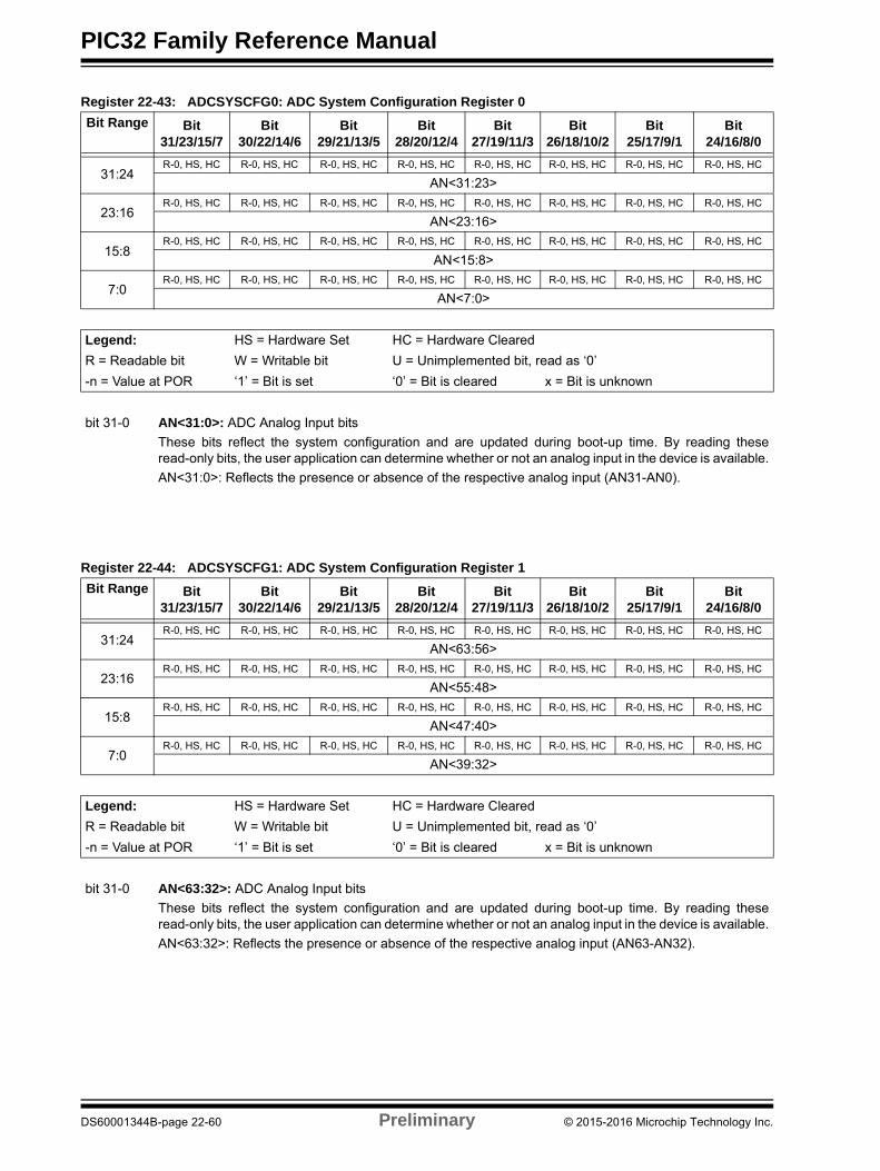
PIC32 Family Reference Manual
Register 22-43: ADCSYSCFG0: ADC System Configuration Register 0
Bit Range Bit31/23/15/7
Bit30/22/14/6
Bit29/21/13/5
Bit28/20/12/4
Bit27/19/11/3
Bit26/18/10/2
Bit25/17/9/1
Bit24/16/8/0
31:24R-0, HS, HC R-0, HS, HC R-0, HS, HC R-0, HS, HC R-0, HS, HC R-0, HS, HC R-0, HS, HC R-0, HS, HC
AN<31:23>
23:16R-0, HS, HC R-0, HS, HC R-0, HS, HC R-0, HS, HC R-0, HS, HC R-0, HS, HC R-0, HS, HC R-0, HS, HC
AN<23:16>
15:8R-0, HS, HC R-0, HS, HC R-0, HS, HC R-0, HS, HC R-0, HS, HC R-0, HS, HC R-0, HS, HC R-0, HS, HC
AN<15:8>
7:0R-0, HS, HC R-0, HS, HC R-0, HS, HC R-0, HS, HC R-0, HS, HC R-0, HS, HC R-0, HS, HC R-0, HS, HC
AN<7:0>
Legend: HS = Hardware Set HC = Hardware Cleared
R = Readable bit W = Writable bit U = Unimplemented bit, read as ‘0’
-n = Value at POR ‘1’ = Bit is set ‘0’ = Bit is cleared x = Bit is unknown
bit 31-0 AN<31:0>: ADC Analog Input bits
These bits reflect the system configuration and are updated during boot-up time. By reading theseread-only bits, the user application can determine whether or not an analog input in the device is available.
AN<31:0>: Reflects the presence or absence of the respective analog input (AN31-AN0).
Register 22-44: ADCSYSCFG1: ADC System Configuration Register 1
Bit Range Bit31/23/15/7
Bit30/22/14/6
Bit29/21/13/5
Bit28/20/12/4
Bit27/19/11/3
Bit26/18/10/2
Bit25/17/9/1
Bit24/16/8/0
31:24R-0, HS, HC R-0, HS, HC R-0, HS, HC R-0, HS, HC R-0, HS, HC R-0, HS, HC R-0, HS, HC R-0, HS, HC
AN<63:56>
23:16R-0, HS, HC R-0, HS, HC R-0, HS, HC R-0, HS, HC R-0, HS, HC R-0, HS, HC R-0, HS, HC R-0, HS, HC
AN<55:48>
15:8R-0, HS, HC R-0, HS, HC R-0, HS, HC R-0, HS, HC R-0, HS, HC R-0, HS, HC R-0, HS, HC R-0, HS, HC
AN<47:40>
7:0R-0, HS, HC R-0, HS, HC R-0, HS, HC R-0, HS, HC R-0, HS, HC R-0, HS, HC R-0, HS, HC R-0, HS, HC
AN<39:32>
Legend: HS = Hardware Set HC = Hardware Cleared
R = Readable bit W = Writable bit U = Unimplemented bit, read as ‘0’
-n = Value at POR ‘1’ = Bit is set ‘0’ = Bit is cleared x = Bit is unknown
bit 31-0 AN<63:32>: ADC Analog Input bits
These bits reflect the system configuration and are updated during boot-up time. By reading theseread-only bits, the user application can determine whether or not an analog input in the device is available.
AN<63:32>: Reflects the presence or absence of the respective analog input (AN63-AN32).
DS60001344B-page 22-60 Preliminary © 2015-2016 Microchip Technology Inc.

Section 22. 12-bit High-Speed SAR ADC
22.3 ADC OPERATION
The High-Speed Successive Approximation Register (SAR) ADC is designed to support powerconversion and motor control applications and consists of up to eight individual ADC modules.The dedicated ADC modules have single analog inputs (after alternate selection) connected totheir S&H circuit. Since these ADC modules sample a dedicated analog input, they are termed“dedicated” ADC modules. Dedicated ADC modules are used to measure/capture time sensitiveor transitory analog signals. The shared ADC module has multiple analog input connected to itsS&H circuit through a multiplexer. Since multiple analog input share this ADC, it is termed the“shared” ADC module. The shared ADC module is used to measure analog signals of lowerfrequencies and signals, which are static in nature (i.e.,do not change significantly with time).
The analog inputs that are connected to the dedicated ADC modules are considered Class 1inputs. The analog inputs connected to the shared ADC module are Class 2 and Class 3 inputs.The number of inputs designated for each “class” depends on the specific device. For example,a device with eight ADC modules and 54 analog inputs will have the following arrangement:
• Class 1 = AN0 to AN6
• Class 2 = AN7 to AN31
• Class 3 = AN32 to AN53
The property of each class of analog input is described in Table 22-2:
Table 22-2: Analog Input Class
Class 1 analog input properties:
• Class 1 inputs are associated with a dedicated ADC module. Each dedicated ADC has a single Class 1 input associated with it at a given time. The (alternate) input selection is made through the SHxALT<1:0> bits in the ADCTRGMODE register. Regardless of the alternate input selection, the trigger source and the result register remains the same.
• Each Class 1 input has a unique trigger (selected by the ADCTRGx register) and upon arrival of the trigger, ends sampling and starts conversion. Upon completion of conversion, the ADC module reverts back to sampling mode. When a Class 1 input is enabled and is not being converted, it is always sampled.
• All Class 1 inputs have same priority, work independently and it is possible to start conversion on all Class 1 inputs at the same time
• Class 1 inputs can be part of a scan list, triggered by the common scan trigger source.
Note: Refer to the “ADC” chapter in the specific device data sheet for the actual numberof analog inputs for each class.
ADC ModuleAnalog Input Class
Trigger Trigger Action
Dedicated ADC modules Class 1 Individual trigger source or scan trigger
Ends sampling and starts conversion
Shared ADC module Class 2 Individual trigger source or scan trigger
Starts sampling sequence or begins scan sequence
Shared ADC module with input scan
Class 3 Scan trigger Starts scan sequence
© 2015-2016 Microchip Technology Inc. Preliminary DS60001344B-page 22-61

PIC32 Family Reference Manual
Figure 22-4: Sample and Conversion Sequence for Dedicated ADC Modules
Class 2 and Class 3 analog input properties:
• Class 2 inputs are used on the shared ADC module, either individually triggered or as part of a scan list. When used individually they are triggered by their unique trigger selected by the ADCTRGx register.
• The analog inputs on the shared ADC have a natural order of priority (for example, AN7 has a higher priority than AN12)
• Class 3 inputs are used exclusively for scanning and share a common trigger source (scan trigger)
• Since Class 3 analog inputs share both the ADC module and the trigger source, the only method possible to convert them is to scan them sequentially for each incoming scan trigger event, where scanning occurs in the natural order of priority
• Unlike Class 1 analog inputs, the arrival of a trigger in the shared ADC module only starts the sampling. When the trigger arrives, the ADC module goes into sampling mode for the sampling time decided by the SAMC<9:0> bits (ADCCON2<25:16>). At the end of sampling, the ADC starts conversion. Upon completion of conversion, the ADC module is used to con-vert the next in line Class 2 or Class 3 inputs, according to the natural order of priority. When a shared analog input (Class 2 or Class 3) has completed all conversion and no trigger is pending, the ADC module is disconnected from all analog inputs.
Figure 22-5: Sample and Conversion Sequence for Shared ADC Modules
Sample SampleHold
Convert
Trigger switches the ADC core (S&H) circuit to a Hold state and the conversion begins
At the end of conversion, data is written to buffer and interrupt is generated (if enabled)
ADC core (S&H) is disconnected from the analog input during Hold
ADC core (S&H) is connected to the analog input for sampling.
(1 clock jitter)
Sample Hold
Convert
Once sampling is complete, the conversion begins
At the end of conversion, data is written to buffer and interrupt is generated (if enabled)
ADC (S&H) is disconnected from the analog input
Disconnected Disconnected
Trigger causes S&H circuit to begin sampling for the specified number of ADC clocks, and then switches to the Hold state.
DS60001344B-page 22-62 Preliminary © 2015-2016 Microchip Technology Inc.
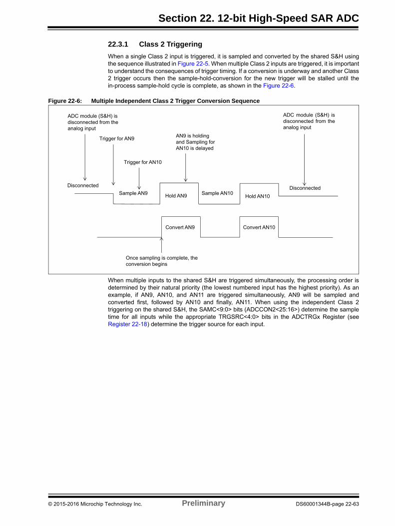
Section 22. 12-bit High-Speed SAR ADC
22.3.1 Class 2 Triggering
When a single Class 2 input is triggered, it is sampled and converted by the shared S&H usingthe sequence illustrated in Figure 22-5. When multiple Class 2 inputs are triggered, it is importantto understand the consequences of trigger timing. If a conversion is underway and another Class2 trigger occurs then the sample-hold-conversion for the new trigger will be stalled until thein-process sample-hold cycle is complete, as shown in the Figure 22-6.
Figure 22-6: Multiple Independent Class 2 Trigger Conversion Sequence
When multiple inputs to the shared S&H are triggered simultaneously, the processing order isdetermined by their natural priority (the lowest numbered input has the highest priority). As anexample, if AN9, AN10, and AN11 are triggered simultaneously, AN9 will be sampled andconverted first, followed by AN10 and finally, AN11. When using the independent Class 2triggering on the shared S&H, the SAMC<9:0> bits (ADCCON2<25:16>) determine the sampletime for all inputs while the appropriate TRGSRC<4:0> bits in the ADCTRGx Register (seeRegister 22-18) determine the trigger source for each input.
Sample AN Hold AN
Convert AN
Once sampling is complete, the conversion begins
ADC (S&H) is disconnected from theanalog input
Disconnected Disconnected
Trigger for AN
Trigger for AN
AN is holding and Sampling forAN is delayed
Sample AN
Convert AN
Hold AN
ADC (S&H) is disconnected from theanalog input
© 2015-2016 Microchip Technology Inc. Preliminary DS60001344B-page 22-63
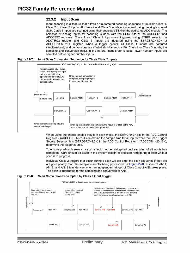
PIC32 Family Reference Manual
22.3.2 Input ScanInput scanning is a feature that allows an automated scanning sequence of multiple Class 1,Class 2 or Class 3 inputs. All Class 2 and Class 3 inputs are scanned using the single sharedS&H. Class 1 inputs are scanned using their dedicated S&H on the dedicated ADC module. Theselection of analog inputs for scanning is done with the CSSx bits of the ADCCSS1 andADCCSS2 registers. Class 1 and Class 2 inputs are triggered using STRIG selection inADCTRGx register and Class 3 inputs are triggered using the STRGSRC<4:0> ofADCCON1<20:16> register. When a trigger occurs, all Class 1 inputs are capturedsimultaneously and conversions are started simultaneously. For Class 2 or Class 3 inputs, thesampling and conversion occur in the natural input order is used; lower number inputs aresampled before higher number inputs.
Figure 22-7: Input Scan Conversion Sequence for Three Class 2 Inputs
When using the shared analog inputs in scan mode, the SAMC<9:0> bits in the ADC ControlRegister 2 (ADCCON2<25:16>) determine the sample time for all inputs while the Scan TriggerSource Selection bits (STRGSRC<4:0>) in the ADC Control Register 1 (ADCCON1<20:16>),determine the trigger source.
To ensure predicable results, a scan should not be retriggered until sampling of all inputs hascompleted. Care should be taken in the system design to preclude retriggering a scan while ascan is in progress.
Individual Class 2 triggers that occur during a scan will pre-empt the scan sequence if they area higher priority than the sample currently being processed. In Figure 22-8, a scan of AN11,AN12, and AN13 is underway when an independent trigger of Class 2 input AN8 takes place.The scan is interrupted for the sampling and conversion of AN8.
Figure 22-8: Scan Conversion Pre-empted by Class 2 Input Trigger
Sample AN Hold AN
Convert AN
Once sampling is complete, the conversion begins
ADC (S&H) is disconnected from the analog input
Disconnected Disconnected
Trigger causes S&H circuit to begin sampling first input in the scan list for the specified number of ADC clocks, and then switches to Hold state.
Once the first conversion is complete, sampling begins for next input in scan list
Sample AN Hold AN
Convert AN
Sample AN Hold AN
Convert AN
When each conversion is complete, the result is written to ADCresult buffer and an interrupt is generated
Sample AN11 Hold AN11
Convert AN11
ADC core (S&H) is disconnected from the analog input
Dis
conn
ecte
d
Dis
conn
ecte
d
Scan trigger starts scan process of inputs AN11, AN12 and AN13
Independent trigger of Class 2 input AN8 occurs here
Sample AN12 Hold AN12
Convert AN12
Sample AN6 Hold AN8
Convert AN8
Sample AN13 Hold AN13
Convert AN13
Sampling and conversion of AN8 pre-empts the scan process. AN8 is sampled and converted between AN12 and AN13, but the arrival of the AN8 trigger does not abort the ongoing sample/conversion of AN12.
DS60001344B-page 22-64 Preliminary © 2015-2016 Microchip Technology Inc.

Section 22. 12-bit High-Speed SAR ADC
22.4 ADC MODULE CONFIGURATION
Operation of the ADC module is directed through bit settings in the specific registers. Thefollowing instructions summarize the actions and the settings. The options and details for eachconfiguration step are provided in the subsequent sections.
To configure the ADC module, perform the following steps:
1. Configure the analog port pins, as described in 22.4.1 “Configuring the Analog PortPins”.
2. Initialize the ADC calibration values by copying them from the factory-programmedDEVADCx Flash registers into the corresponding ADCxCFG registers.
3. Select the analog inputs to the ADC multiplexers, as described in 22.4.2 “Selecting theADC Multiplexer Analog Inputs”.
4. Select the format of the ADC result, as described in 22.4.3 “Selecting the Format of theADC Result”.
5. Select the conversion trigger source, as described in 22.4.4 “Selecting the ConversionTrigger Source”.
6. Select the voltage reference source, as described in 22.4.5 “Selecting the VoltageReference Source”.
7. Select the scanned inputs, as described in 22.4.6 “Selecting the Scanned Inputs”.
8. Select the analog-to-digital conversion clock source and prescaler, as described in22.4.7 “Selecting the Analog-to-Digital Conversion Clock Source and Prescaler”.
9. Specify any additional acquisition time, if required, as described in 22.10 “ADC SamplingRequirements”.
10. Turn on the ADC module, as described in 22.4.9 “Turning ON the ADC”.
11. Poll (or wait for the interrupt) for the voltage reference to be ready, as described in22.4.5 “Selecting the Voltage Reference Source”.
12. Enable the analog and bias circuit for required ADC modules and after the ADC modulewakes-up, enable the digital circuit, as described in 22.7.3 “ADC Low-power Mode”
13. Configure the ADC interrupts (if required), as described in 22.6 “Interrupts”.
22.4.1 Configuring the Analog Port Pins
The ANSELx registers for the I/O ports associated with the analog inputs are used to configurethe corresponding pin as an analog or a digital pin. A pin is configured as analog input when thecorresponding ANSELx bit = 1. When the ANSELx bit = 0, the pin is set to digital control. TheANSELx registers are set when the device comes out of Reset, causing the ADC input pins to beconfigured as analog inputs by default.
The TRISx registers control the digital function of the port pins. The port pins that are requiredas analog inputs must have their corresponding bit set in the specific TRISx register, configuringthe pin as an input. If the I/O pin associated with an ADC input is configured as an output byclearing the TRISx bit, the port’s digital output level (VOH or VOL) will be converted. After a deviceReset, all of the TRISx bits are set. For more information on port pin configuration, refer to the“I/O Ports” chapter of the specific device data sheet.
Note: When reading a PORT register that shares pins with the ADC, any pin configuredas an analog input reads as a ‘0’ when the PORT latch is read. Analog levels on anypin that is defined as a digital input but not configured as an analog input, may causethe input buffer to consume current that exceeds the device specification.
© 2015-2016 Microchip Technology Inc. Preliminary DS60001344B-page 22-65
PIC32 Family Reference Manual
Example 22-1: Initializing and Using ADC Class 1 Input
int main(int argc, char** argv) {int result[3];
/* initialize ADC calibration setting */ ADC0CFG = DEVADC0; ADC1CFG = DEVADC1; ADC2CFG = DEVADC2; ADC3CFG = DEVADC3; ADC4CFG = DEVADC4; ADC5CFG = DEVADC5; ADC6CFG = DEVADC6; ADC7CFG = DEVADC7;
/* Configure ADCCON1 */ADCCON1 = 0; // No ADCCON1 features are enabled including: Stop-in-Idle, turbo,
// CVD mode, Fractional mode and scan trigger source.
/* Configure ADCCON2 */ADCCON2 = 0; // Since, we are using only the Class 1 inputs, no setting is
// required for ADCDIV
/* Initialize warm up time register */ADCANCON = 0;ADCANCONbits.WKUPCLKCNT = 5; // Wakeup exponent = 32 * TADx
/* Clock setting */ADCCON3 = 0;ADCCON3bits.ADCSEL = 0; // Select input clock sourceADCCON3bits.CONCLKDIV = 1; // Control clock frequency is half of input clockADCCON3bits.VREFSEL = 0; // Select AVDD and AVSS as reference source
/* Select ADC sample time and conversion clock */ADC0TIMEbits.ADCDIV = 1; // ADC0 clock frequency is half of control clock = TAD0ADC0TIMEbits.SAMC = 5; // ADC0 sampling time = 5 * TAD0ADC0TIMEbits.SELRES = 3; // ADC0 resolution is 12 bitsADC1TIMEbits.ADCDIV = 1; // ADC1 clock frequency is half of control clock = TAD1ADC1TIMEbits.SAMC = 5; // ADC1 sampling time = 5 * TAD1ADC1TIMEbits.SELRES = 3; // ADC1 resolution is 12 bitsADC2TIMEbits.ADCDIV = 1; // ADC2 clock frequency is half of control clock = TAD2ADC2TIMEbits.SAMC = 5; // ADC2 sampling time = 5 * TAD2ADC2TIMEbits.SELRES = 3; // ADC2 resolution is 12 bits
/* Select analog input for ADC modules, no presync trigger, not sync sampling */ADCTRGMODEbits.SH0ALT = 0; // ADC0 = AN0ADCTRGMODEbits.SH1ALT = 0; // ADC1 = AN1ADCTRGMODEbits.SH2ALT = 0; // ADC2 = AN2
/* Select ADC input mode */ADCIMCON1bits.SIGN0 = 0; // unsigned data formatADCIMCON1bits.DIFF0 = 0; // Single ended modeADCIMCON1bits.SIGN1 = 0; // unsigned data formatADCIMCON1bits.DIFF1 = 0; // Single ended modeADCIMCON1bits.SIGN2 = 0; // unsigned data formatADCIMCON1bits.DIFF2 = 0; // Single ended mode
/* Configure ADCGIRQENx */ADCGIRQEN1 = 0; // No interrupts are usedADCGIRQEN2 = 0;
/* Configure ADCCSSx */ADCCSS1 = 0; // No scanning is usedADCCSS2 = 0;
/* Configure ADCCMPCONx */ADCCMPCON1 = 0; // No digital comparators are used. Setting the ADCCMPCONxADCCMPCON2 = 0; // register to '0' ensures that the comparator is disabled.ADCCMPCON3 = 0; // Other registers are “don't care”.ADCCMPCON4 = 0;ADCCMPCON5 = 0;ADCCMPCON6 = 0;
DS60001344B-page 22-66 Preliminary © 2015-2016 Microchip Technology Inc.

Section 22. 12-bit High-Speed SAR ADC
Example 22-1: Initializing and Using ADC Class 1 Input (Continued)/* Configure ADCFLTRx */ADCFLTR1 = 0; // No oversampling filters are used.ADCFLTR2 = 0;ADCFLTR3 = 0;ADCFLTR4 = 0;ADCFLTR5 = 0;ADCFLTR6 = 0;
/* Set up the trigger sources */ADCTRGSNSbits.LVL0 = 0; // Edge triggerADCTRGSNSbits.LVL1 = 0; // Edge triggerADCTRGSNSbits.LVL2 = 0; // Edge triggerADCTRG1bits.TRGSRC0 = 1; // Set AN0 to trigger from software.ADCTRG1bits.TRGSRC1 = 1; // Set AN1 to trigger from software.ADCTRG1bits.TRGSRC2 = 1; // Set AN2 to trigger from software.
/* Early interrupt */ADCEIEN1 = 0; // No early interruptADCEIEN2 = 0;
/* Turn the ADC on */ADCCON1bits.ON = 1;
/* Wait for voltage reference to be stable */while(!ADCCON2bits.BGVRRDY); // Wait until the reference voltage is readywhile(ADCCON2bits.REFFLT); // Wait if there is a fault with the reference voltage
/* Enable clock to analog circuit */ADCANCONbits.ANEN0 = 1; // Enable the clock to analog biasADCANCONbits.ANEN1 = 1; // Enable the clock to analog biasADCANCONbits.ANEN2 = 1; // Enable the clock to analog bias
/* Wait for ADC to be ready */while(!ADCANCONbits.WKRDY0); // Wait until ADC0 is readywhile(!ADCANCONbits.WKRDY1); // Wait until ADC1 is readywhile(!ADCANCONbits.WKRDY2); // Wait until ADC2 is ready
/* Enable the ADC module */ADCCON3bits.DIGEN0 = 1; // Enable ADC0ADCCON3bits.DIGEN1 = 1; // Enable ADC1ADCCON3bits.DIGEN2 = 1; // Enable ADC2
while (1) {/* Trigger a conversion */ADCCON3bits.GSWTRG = 1;
/* Wait the conversions to complete */while (ADCDSTAT1bits.ARDY0 == 0);/* fetch the result */result[0] = ADCDATA0;
while (ADCDSTAT1bits.ARDY1 == 0);/* fetch the result */result[1] = ADCDATA1;
while (ADCDSTAT1bits.ARDY2 == 0);/* fetch the result */result[2] = ADCDATA2;
/** Process results here** Note: Loop time determines the sampling time since all inputs are Class 1.* If the loop time is small and the next trigger happens before the completion* of set sample time, the conversion will happen only after the sample time* has elapsed.**/
}return (1);}
© 2015-2016 Microchip Technology Inc. Preliminary DS60001344B-page 22-67
PIC32 Family Reference Manual
22.4.2 Selecting the ADC Multiplexer Analog Inputs
Each ADC module has two inputs referred to as the positive and negative inputs. Input selectionoptions vary for the dedicated and shared ADC module are described in the following sections.
22.4.2.1 SELECTION OF POSITIVE INPUTS
For dedicated ADC modules, four alternate selection is provided for each positive input. Thisalternate input can be chosen using the SHxALT<1:0> bits in the ADC Triggering Mode Register(ADCTRGMODE) as follows:
• SH0ALT<1:0> (ADCTRGMODE<17:16>)
• SH1ALT<1:0> (ADCTRGMODE<19:18>)
• SH2ALT<1:0> (ADCTRGMODE<21:20>)
• SH3ALT<1:0> (ADCTRGMODE<23:22>)
• SH4ALT<1:0> (ADCTRGMODE<25:24>)
• SH5ALT<1:0> (ADCTRGMODE<27:26>)
• SH6ALT<1:0> (ADCTRGMODE<29:28>)
Refer to the device data sheet for possible alternate selection of ADC inputs.
For the shared ADC module, the positive input is shared among all Class 2 and Class 3 inputs.Input connection of the analog input ANx to the shared ADC is automatic for either Class 2 inputtrigger or during a scan of Class 2 and or Class 3 inputs. Selecting inputs for scanning isdiscussed separately in 22.4.6 “Selecting the Scanned Inputs”.
22.4.2.2 SELECTION OF NEGATIVE INPUTS
Negative input selection is determined by the setting of the DIFFx bit of the ADCIMCONx register.The DIFFx bit allows the inputs to be rail-to-rail, and either single-ended or differential. TheSIGNx and DIFFx bits in the ADCIMCONx registers scale the internal ADC analog inputs andreference voltages and configure the digital result to align with the expected full-scale outputrange.
For the shared ADC module, the analog inputs have individual settings for the DIFFx bit.Therefore, the user has the ability to select certain inputs as single-ended and others asdifferential, while being connected to the same shared ADC module. While sampling, the signalwill change on-the-fly as single-ended or differential, according to its corresponding DIFFx bitsetting.
Table 22-3: Negative Input Selection
ADCIMCON1 Input Configuration
Input Voltage OutputDIFFx SIGNx
1 1Differential 2’s complement
Minimum input VINP - VINN = -VREF -2048
Maximum input VINP - VINN = VREF +2047
1 0Differential unipolar
Minimum input VINP - VINN = -VREF 0
Maximum input VINP - VINN = VREF +4095
0 1Single-ended 2’s complement
Minimum input VINP = VREF -2048
Maximum input VINP - VINN = VREF +2047
0 0Single-ended unipolar
Minimum input VINP = VREF 0
Maximum input VINP - VINN = VREF +4095
Legend: VINP = Positive S&H input; VINN = Negative S&H input; VREF = VREFH - VREFL
Note: For proper operation and to prevent device damage, input voltage levels should notexceed the limits listed in the “Electrical Characteristics” chapter of the specificdevice data sheet.
DS60001344B-page 22-68 Preliminary © 2015-2016 Microchip Technology Inc.

Section 22. 12-bit High-Speed SAR ADC
22.4.3 Selecting the Format of the ADC Result
The data in the ADC Result register can be read in any of the four supported data formats. Theuser can select from unsigned integer, signed integer, unsigned fractional, or signed fractional.Integer data is right-justified and fractional data is left-justified.
• The integer or fractional data format selection is specified globally for all analog inputs using the Fractional Data Output Format bit, FRACT (ADCCON1<23>)
• The signed or unsigned data format selection can be independently specified for each individual analog input using the SIGNx bits in the ADCIMCONx registers.
Table 22-4 illustrates how a result is formatted.
Table 22-4: ADC Result Format Results
FRACT SIGNx Description 32-bit Output Data Format
0 0 Unsigned integer0000 0000 0000 0000
0000 dddd dddd dddd
0 1 Signed integerssss ssss ssss ssss
ssss sddd dddd dddd
1 0 Fractionaldddd dddd dddd 0000
0000 0000 0000 0000
1 1 Signed fractionalsddd dddd dddd dddd
0000 0000 0000 0000
© 2015-2016 Microchip Technology Inc. Preliminary DS60001344B-page 22-69
PIC32 Family Reference Manual
Example 22-2: ADC Class 2 Configuration and Fractional Formatint main(int argc, char** argv) {
int result[3];
/* Configure ADCCON1 */ADCCON1bits.FRACT = 1; // use Fractional output formatADCCON1bits.SELRES = 3; // ADC7 resolution is 12 bitsADCCON1bits.STRGSRC = 0; // No scan trigger.
/* Configure ADCCON2 */ADCCON2bits.SAMC = 5; // ADC7 sampling time = 5 * TAD7ADCCON2bits.ADCDIV = 1; // ADC7 clock freq is half of control clock = TAD7
/* Initialize warm up time register */ADCANCON = 0;ADCANCONbits.WKUPCLKCNT = 5; // Wakeup exponent = 32 * TADx
/* Clock setting */ADCCON3 = 0;ADCCON3bits.ADCSEL = 0; // Select input clock sourceADCCON3bits.CONCLKDIV = 1; // Control clock frequency is half of input clockADCCON3bits.VREFSEL = 0; // Select AVDD and AVSS as reference source
/* No selection for dedicated ADC modules, no presync trigger, not sync sampling */ADCTRGMODEbits = 0;
/* Select ADC input mode */ADCIMCON1bits.SIGN7 = 0; // unsigned data formatADCIMCON1bits.DIFF7 = 0; // Single ended modeADCIMCON1bits.SIGN8 = 0; // unsigned data formatADCIMCON1bits.DIFF8 = 0; // Single ended modeADCIMCON1bits.SIGN9 = 0; // unsigned data formatADCIMCON1bits.DIFF9 = 0; // Single ended mode
/* Configure ADCGIRQENx */ADCGIRQEN1 = 0; // No interrupts are usedADCGIRQEN2 = 0;
/* Configure ADCCSSx */ADCCSS1 = 0; // No scanning is usedADCCSS2 = 0;
/* Configure ADCCMPCONx */ADCCMPCON1 = 0; // No digital comparators are used. Setting the ADCCMPCONxADCCMPCON2 = 0; // register to '0' ensures that the comparator is disabled.ADCCMPCON3 = 0; // Other registers are “don't care”.ADCCMPCON4 = 0;ADCCMPCON5 = 0;ADCCMPCON6 = 0;
/* Configure ADCFLTRx */ADCFLTR1 = 0; // No oversampling filters are used.ADCFLTR2 = 0;ADCFLTR3 = 0;ADCFLTR4 = 0;ADCFLTR5 = 0;ADCFLTR6 = 0;/* Set up the trigger sources */ADCTRGSNSbits.LVL7 = 0; // Edge triggerADCTRGSNSbits.LVL8 = 0; // Edge triggerADCTRGSNSbits.LVL9 = 0; // Edge triggerADC1TRG2bits.TRGSRC7 = 1; // Set AN7 to trigger from softwareADC2TRG3bits.TRGSRC8 = 1; // Set AN8 to trigger from softwareADC2TRG3bits.TRGSRC9 = 1; // Set AN9 to trigger from software
DS60001344B-page 22-70 Preliminary © 2015-2016 Microchip Technology Inc.

Section 22. 12-bit High-Speed SAR ADC
Example 22-2: ADC Class 2 Configuration and Fractional Format (Continued)/* Early interrupt */ADCEIEN1 = 0; // No early interruptADCEIEN2 = 0;
/* Turn the ADC on */ADCCON1bits.ON = 1;
/* Wait for voltage reference to be stable */while(!ADCCON2bits.BGVRRDY); // Wait until the reference voltage is readywhile(ADCCON2bits.REFFLT); // Wait if there is a fault with the reference voltage
/* Enable clock to analog circuit */ADCANCONbits.ANEN7 = 1; // Enable the clock to analog bias
/* Wait for ADC to be ready */while(!ADCANCONbits.WKRDY7); // Wait until ADC7 is ready
/* Enable the ADC module */ADCCON3bits.DIGEN7 = 1; // Enable ADC7
while (1) {/* Trigger a conversion */ADCCON3bits.GSWTRG = 1;
/* Wait the conversions to complete */while (ADCDSTAT1bits.ARDY7 == 0);/* fetch the result */result[0] = ADCDATA7;
while (ADCDSTAT1bits.ARDY8 == 0);/* fetch the result */result[1] = ADCDATA8;
while (ADCDSTAT1bits.ARDY9 == 0);/* fetch the result */result[2] = ADCDATA9;
/** Process results here** Note 1: Loop time determines the sampling time since all inputs are Class 2.* If the loop time happens is small and the next trigger happens before the* completion of set sample time, the conversion will happen only after the* sample time has elapsed.** Note 2: Results are in fractional format**/
}return (1);
}
© 2015-2016 Microchip Technology Inc. Preliminary DS60001344B-page 22-71
PIC32 Family Reference Manual
22.4.4 Selecting the Conversion Trigger Source
Class 1 and Class 2 inputs to the ADC module can be triggered for conversion either individually,or as part of a scan sequence. Class 3 inputs can only be triggered as part of a scan sequence.Individual or scan triggers can originate from an on-board timer or output compare peripheralevent, from external digital circuits connected to INT0, from external analog circuits connected toan analog comparator, or through software by setting a trigger bit in a SFR.
22.4.4.1 TRIGGER SELECTION FOR CLASS 1 AND CLASS 2 INPUTS
For each one of the Class 1 and Class 2 inputs, the user application can independently specifya conversion trigger source. The individual trigger source for an analog input ‘x’ is specified bythe TRGSRC<4:0> bits located in registers ADCTRG1 through ADCTRG8. Refer to the “ADC”chapter of the specific device data sheet for more information on the available conversion triggeroptions. For example, these trigger sources may include:
• General Purpose (GP) Timers: When a period match occurs for the 32-bit timer, Timer3/2 or Timer5/4, or the 16-bit Timer1, Timer3 or Timer5, a special ADC trigger event signal is generated by the timer. This feature does not exist for other timers. For more information, refer to Section 14. “Timers” (DS60001105) and the “Timer” chapters in the specific device data sheet.
• Output Compare: The Output Compare peripherals, OC1, OC3, and OC5, can be used to generate an ADC trigger then the output transitions from a low to high state. For more information, refer to Section 16. “Output Compare” (DS60001111), and the “Output Compare” chapter in the specific device data sheet.
• Comparators: The analog Comparators can be used to generate an ADC trigger when the output transitions from a low state to a high state. For more information, refer to Section 19. “Comparator” (DS60001110), and the “Comparator” chapter in the specific device data sheet.
• External INT0 Pin Trigger: In this mode, the ADC module starts a conversion on an active transition on the INT0 pin. The INT0 pin may be programmed for either a rising edge input or a falling edge input to trigger the conversion process.
• Global Software Trigger: The ADC module can be configured for manually triggering a con-version for all inputs that have selected this trigger option. The user can manually trigger a conversion by setting the Global Software Trigger bit, GSWTRG (ADCCON3<6>).
22.4.4.2 PRESYNCHRONIZED TRIGGER AND ASYNCHRONOUS SAMPLING FOR CLASS 1 ANALOG INPUTS
The ADCTRGx register is used for ADC triggers.
• Converted data can be stored in dedicated output registers (ADCDATAx)
• Converted data can be stored in the FIFO
• Converted data can be stored in system RAM using the DMA engine
The ADCTRGMODE register contains the trigger mode for the ADC module determined by theSTRGEN bit (presynchronized trigger enable) and the SSAMPEN bit (synchronous samplingalso for the first sample after being idle or disabled).
Note: When conversion triggers for multiple Class 2 analog inputs occur simultaneously,they are prioritized according to a natural order priority scheme based on the analoginput used. AN7 has the highest priority, AN8 has the next highest priority, etc.
Note 1: The trigger and synchronization works on “control clock (TQ)”. But the samplingtime (tSAMCx) is based on TADX clock (which is derived from the TQ signal after pass-ing through a divisor).
2: When Synchronous sampling is used (SSAMPEN = 1), the presynchronized triggervalue is ignored (STRGEN = “don’t care”).
DS60001344B-page 22-72 Preliminary © 2015-2016 Microchip Technology Inc.
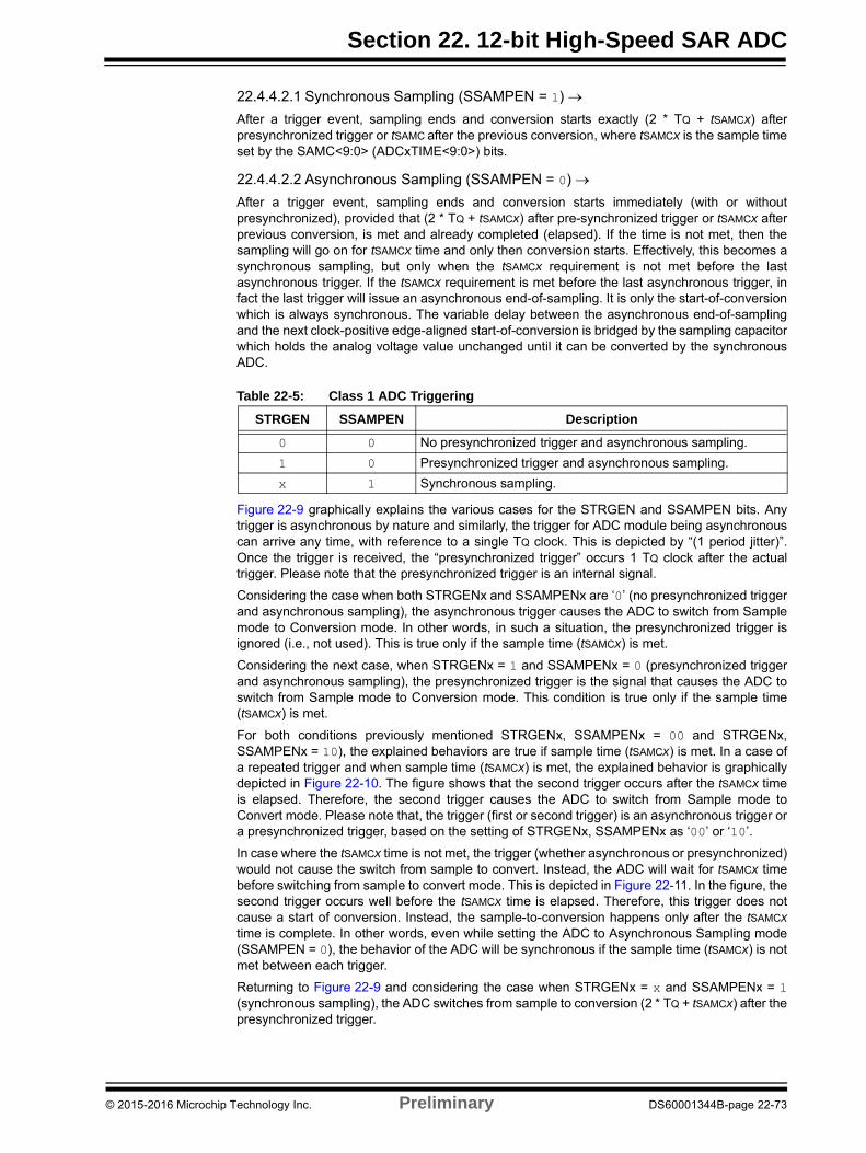
Section 22. 12-bit High-Speed SAR ADC
22.4.4.2.1 Synchronous Sampling (SSAMPEN = 1)
After a trigger event, sampling ends and conversion starts exactly (2 * TQ + tSAMCx) afterpresynchronized trigger or tSAMC after the previous conversion, where tSAMCx is the sample timeset by the SAMC<9:0> (ADCxTIME<9:0>) bits.
22.4.4.2.2 Asynchronous Sampling (SSAMPEN = 0)
After a trigger event, sampling ends and conversion starts immediately (with or withoutpresynchronized), provided that (2 * TQ + tSAMCx) after pre-synchronized trigger or tSAMCx afterprevious conversion, is met and already completed (elapsed). If the time is not met, then thesampling will go on for tSAMCx time and only then conversion starts. Effectively, this becomes asynchronous sampling, but only when the tSAMCx requirement is not met before the lastasynchronous trigger. If the tSAMCx requirement is met before the last asynchronous trigger, infact the last trigger will issue an asynchronous end-of-sampling. It is only the start-of-conversionwhich is always synchronous. The variable delay between the asynchronous end-of-samplingand the next clock-positive edge-aligned start-of-conversion is bridged by the sampling capacitorwhich holds the analog voltage value unchanged until it can be converted by the synchronousADC.
Table 22-5: Class 1 ADC Triggering
Figure 22-9 graphically explains the various cases for the STRGEN and SSAMPEN bits. Anytrigger is asynchronous by nature and similarly, the trigger for ADC module being asynchronouscan arrive any time, with reference to a single TQ clock. This is depicted by “(1 period jitter)”.Once the trigger is received, the “presynchronized trigger” occurs 1 TQ clock after the actualtrigger. Please note that the presynchronized trigger is an internal signal.
Considering the case when both STRGENx and SSAMPENx are ‘0’ (no presynchronized triggerand asynchronous sampling), the asynchronous trigger causes the ADC to switch from Samplemode to Conversion mode. In other words, in such a situation, the presynchronized trigger isignored (i.e., not used). This is true only if the sample time (tSAMCx) is met.
Considering the next case, when STRGENx = 1 and SSAMPENx = 0 (presynchronized triggerand asynchronous sampling), the presynchronized trigger is the signal that causes the ADC toswitch from Sample mode to Conversion mode. This condition is true only if the sample time(tSAMCx) is met.
For both conditions previously mentioned STRGENx, SSAMPENx = 00 and STRGENx,SSAMPENx = 10), the explained behaviors are true if sample time (tSAMCx) is met. In a case ofa repeated trigger and when sample time (tSAMCx) is met, the explained behavior is graphicallydepicted in Figure 22-10. The figure shows that the second trigger occurs after the tSAMCx timeis elapsed. Therefore, the second trigger causes the ADC to switch from Sample mode toConvert mode. Please note that, the trigger (first or second trigger) is an asynchronous trigger ora presynchronized trigger, based on the setting of STRGENx, SSAMPENx as ‘00’ or ‘10’.
In case where the tSAMCx time is not met, the trigger (whether asynchronous or presynchronized)would not cause the switch from sample to convert. Instead, the ADC will wait for tSAMCx timebefore switching from sample to convert mode. This is depicted in Figure 22-11. In the figure, thesecond trigger occurs well before the tSAMCx time is elapsed. Therefore, this trigger does notcause a start of conversion. Instead, the sample-to-conversion happens only after the tSAMCxtime is complete. In other words, even while setting the ADC to Asynchronous Sampling mode(SSAMPEN = 0), the behavior of the ADC will be synchronous if the sample time (tSAMCx) is notmet between each trigger.
Returning to Figure 22-9 and considering the case when STRGENx = x and SSAMPENx = 1(synchronous sampling), the ADC switches from sample to conversion (2 * TQ + tSAMCx) after thepresynchronized trigger.
STRGEN SSAMPEN Description
0 0 No presynchronized trigger and asynchronous sampling.
1 0 Presynchronized trigger and asynchronous sampling.
x 1 Synchronous sampling.
© 2015-2016 Microchip Technology Inc. Preliminary DS60001344B-page 22-73
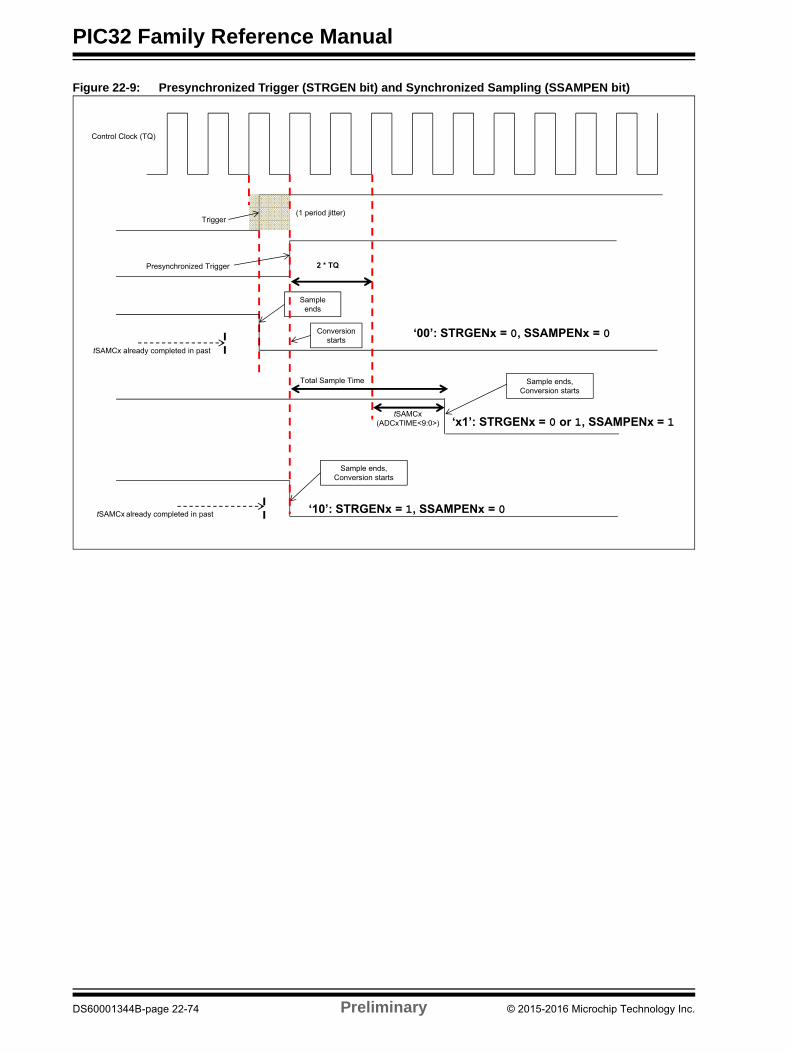
PIC32 Family Reference Manual
Figure 22-9: Presynchronized Trigger (STRGEN bit) and Synchronized Sampling (SSAMPEN bit)
Control Clock (TQ)
Trigger(1 period jitter)
Presynchronized Trigger
Sampleends
‘00’: STRGENx = 0, SSAMPENx = 0
ADCxTIME<9:0>
2 * TQ
‘10’: STRGENx = 1, SSAMPENx = 0
Sample ends, Conversion starts
tSAMCx already completed in past
tSAMCx already completed in past
Conversionstarts
Sample ends, Conversion starts
DS60001344B-page 22-74 Preliminary © 2015-2016 Microchip Technology Inc.
Section 22. 12-bit High-Speed SAR ADC
Figure 22-10: Asynchronous Sampling (SSAMPEN = 0) (When trigger is at rate such that tSAMCx is met, the ADC allows asynchronous trigger to start conversion)
Trigger
Sample
Convert
tSAMCx
tCONVERT
First TriggerSecond Trigger occurred after tSAMCx
1 TQ jitter1 TQ jitter
© 2015-2016 Microchip Technology Inc. Preliminary DS60001344B-page 22-75
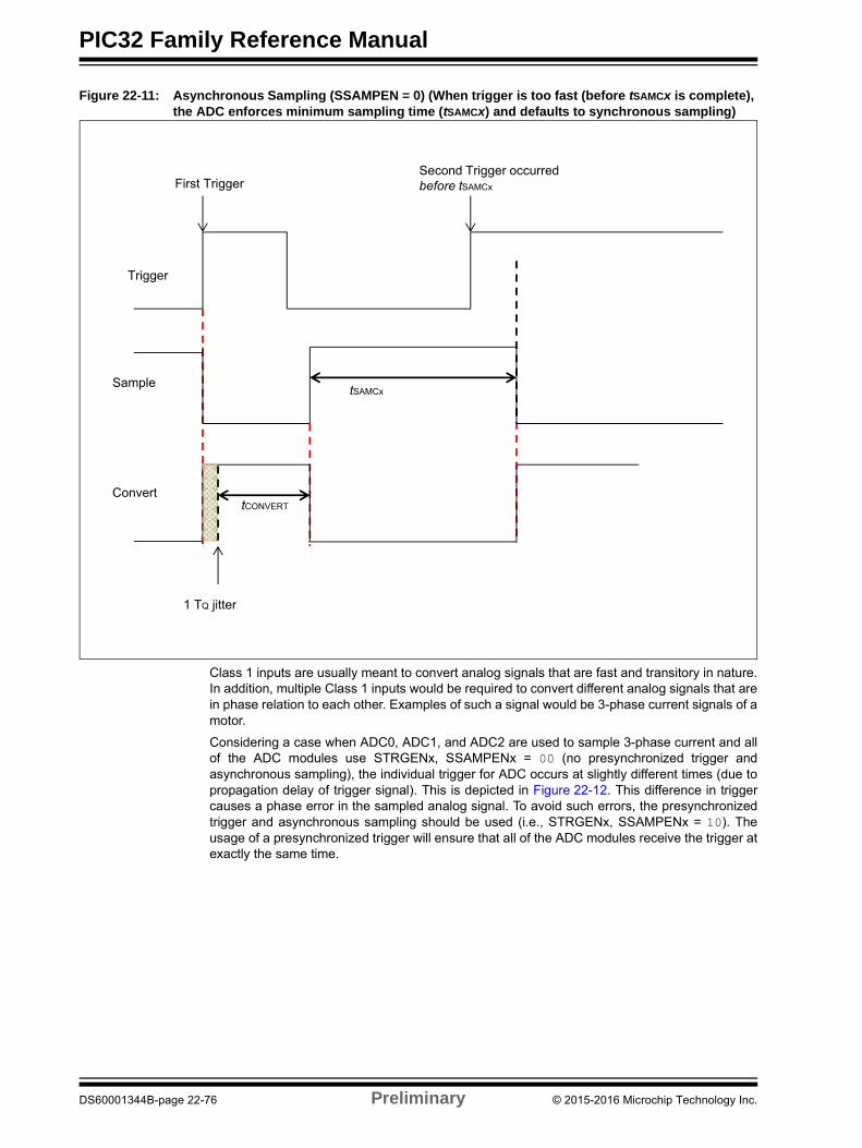
PIC32 Family Reference Manual
Figure 22-11: Asynchronous Sampling (SSAMPEN = 0) (When trigger is too fast (before tSAMCx is complete), the ADC enforces minimum sampling time (tSAMCx) and defaults to synchronous sampling)
Class 1 inputs are usually meant to convert analog signals that are fast and transitory in nature.In addition, multiple Class 1 inputs would be required to convert different analog signals that arein phase relation to each other. Examples of such a signal would be 3-phase current signals of amotor.
Considering a case when ADC0, ADC1, and ADC2 are used to sample 3-phase current and allof the ADC modules use STRGENx, SSAMPENx = 00 (no presynchronized trigger andasynchronous sampling), the individual trigger for ADC occurs at slightly different times (due topropagation delay of trigger signal). This is depicted in Figure 22-12. This difference in triggercauses a phase error in the sampled analog signal. To avoid such errors, the presynchronizedtrigger and asynchronous sampling should be used (i.e., STRGENx, SSAMPENx = 10). Theusage of a presynchronized trigger will ensure that all of the ADC modules receive the trigger atexactly the same time.
Trigger
Sample
Convert
tSAMCx
tCONVERT
First TriggerSecond Trigger occurred before tSAMCx
1 TQ jitter
DS60001344B-page 22-76 Preliminary © 2015-2016 Microchip Technology Inc.
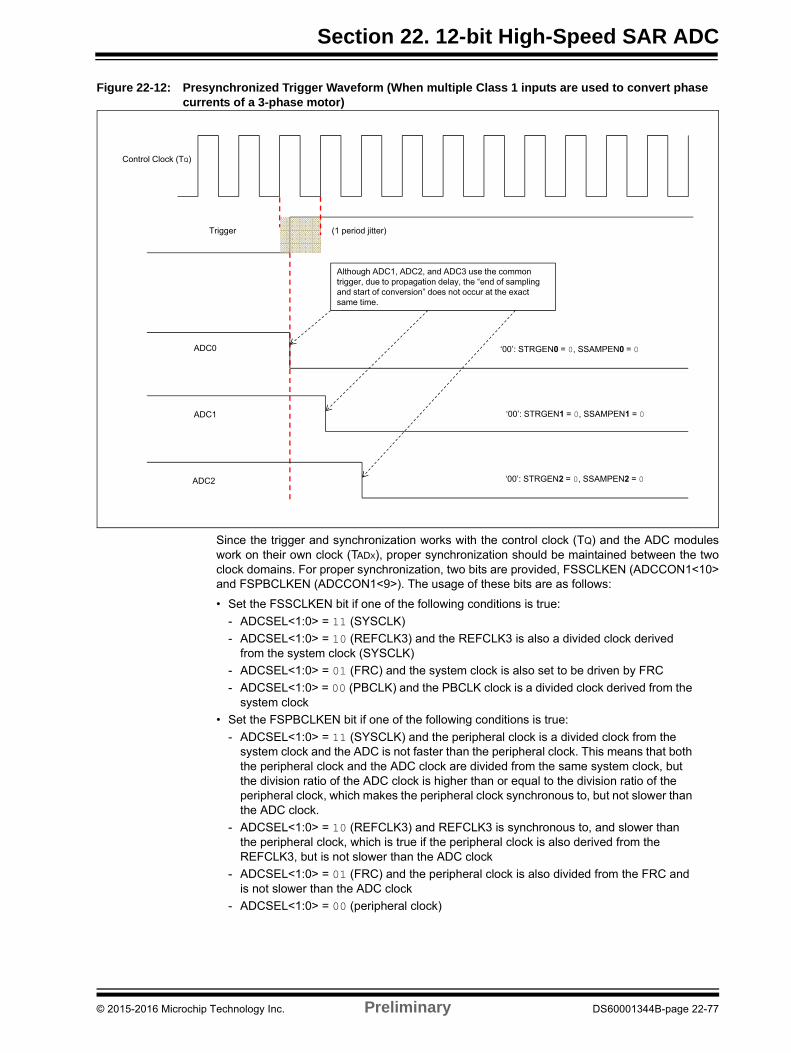
Section 22. 12-bit High-Speed SAR ADC
Figure 22-12: Presynchronized Trigger Waveform (When multiple Class 1 inputs are used to convert phase currents of a 3-phase motor)
Since the trigger and synchronization works with the control clock (TQ) and the ADC moduleswork on their own clock (TADX), proper synchronization should be maintained between the twoclock domains. For proper synchronization, two bits are provided, FSSCLKEN (ADCCON1<10>and FSPBCLKEN (ADCCON1<9>). The usage of these bits are as follows:
• Set the FSSCLKEN bit if one of the following conditions is true:
- ADCSEL<1:0> = 11 (SYSCLK)
- ADCSEL<1:0> = 10 (REFCLK3) and the REFCLK3 is also a divided clock derived from the system clock (SYSCLK)
- ADCSEL<1:0> = 01 (FRC) and the system clock is also set to be driven by FRC
- ADCSEL<1:0> = 00 (PBCLK) and the PBCLK clock is a divided clock derived from the system clock
• Set the FSPBCLKEN bit if one of the following conditions is true:
- ADCSEL<1:0> = 11 (SYSCLK) and the peripheral clock is a divided clock from the system clock and the ADC is not faster than the peripheral clock. This means that both the peripheral clock and the ADC clock are divided from the same system clock, but the division ratio of the ADC clock is higher than or equal to the division ratio of the peripheral clock, which makes the peripheral clock synchronous to, but not slower than the ADC clock.
- ADCSEL<1:0> = 10 (REFCLK3) and REFCLK3 is synchronous to, and slower than the peripheral clock, which is true if the peripheral clock is also derived from the REFCLK3, but is not slower than the ADC clock
- ADCSEL<1:0> = 01 (FRC) and the peripheral clock is also divided from the FRC and is not slower than the ADC clock
- ADCSEL<1:0> = 00 (peripheral clock)
Control Clock (TQ)
Trigger (1 period jitter)
Although ADC1, ADC2, and ADC3 use the common trigger, due to propagation delay, the “end of sampling and start of conversion” does not occur at the exact same time.
‘00’: STRGEN0 = 0, SSAMPEN0 = 0
‘00’: STRGEN1 = 0, SSAMPEN1 = 0
‘00’: STRGEN2 = 0, SSAMPEN2 = 0
ADC0
ADC1
ADC2
© 2015-2016 Microchip Technology Inc. Preliminary DS60001344B-page 22-77
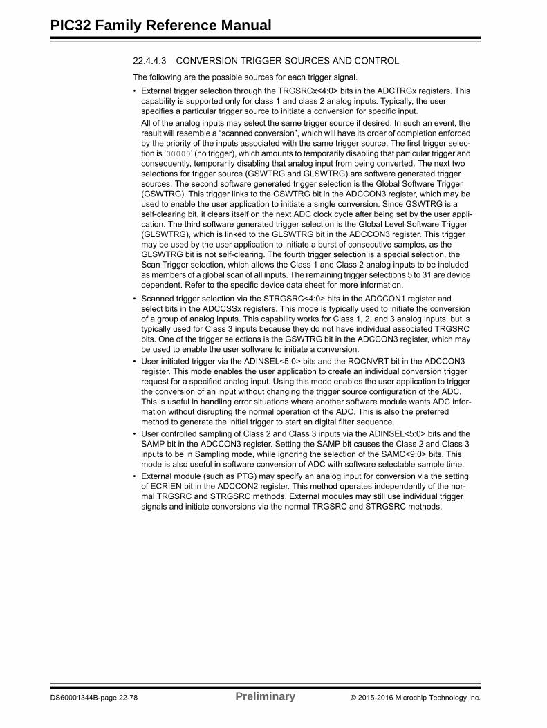
PIC32 Family Reference Manual
22.4.4.3 CONVERSION TRIGGER SOURCES AND CONTROL
The following are the possible sources for each trigger signal.
• External trigger selection through the TRGSRCx<4:0> bits in the ADCTRGx registers. This capability is supported only for class 1 and class 2 analog inputs. Typically, the user specifies a particular trigger source to initiate a conversion for specific input.
All of the analog inputs may select the same trigger source if desired. In such an event, the result will resemble a “scanned conversion”, which will have its order of completion enforced by the priority of the inputs associated with the same trigger source. The first trigger selec-tion is ‘00000’ (no trigger), which amounts to temporarily disabling that particular trigger and consequently, temporarily disabling that analog input from being converted. The next two selections for trigger source (GSWTRG and GLSWTRG) are software generated trigger sources. The second software generated trigger selection is the Global Software Trigger (GSWTRG). This trigger links to the GSWTRG bit in the ADCCON3 register, which may be used to enable the user application to initiate a single conversion. Since GSWTRG is a self-clearing bit, it clears itself on the next ADC clock cycle after being set by the user appli-cation. The third software generated trigger selection is the Global Level Software Trigger (GLSWTRG), which is linked to the GLSWTRG bit in the ADCCON3 register. This trigger may be used by the user application to initiate a burst of consecutive samples, as the GLSWTRG bit is not self-clearing. The fourth trigger selection is a special selection, the Scan Trigger selection, which allows the Class 1 and Class 2 analog inputs to be included as members of a global scan of all inputs. The remaining trigger selections 5 to 31 are device dependent. Refer to the specific device data sheet for more information.
• Scanned trigger selection via the STRGSRC<4:0> bits in the ADCCON1 register and select bits in the ADCCSSx registers. This mode is typically used to initiate the conversion of a group of analog inputs. This capability works for Class 1, 2, and 3 analog inputs, but is typically used for Class 3 inputs because they do not have individual associated TRGSRC bits. One of the trigger selections is the GSWTRG bit in the ADCCON3 register, which may be used to enable the user software to initiate a conversion.
• User initiated trigger via the ADINSEL<5:0> bits and the RQCNVRT bit in the ADCCON3 register. This mode enables the user application to create an individual conversion trigger request for a specified analog input. Using this mode enables the user application to trigger the conversion of an input without changing the trigger source configuration of the ADC. This is useful in handling error situations where another software module wants ADC infor-mation without disrupting the normal operation of the ADC. This is also the preferred method to generate the initial trigger to start an digital filter sequence.
• User controlled sampling of Class 2 and Class 3 inputs via the ADINSEL<5:0> bits and the SAMP bit in the ADCCON3 register. Setting the SAMP bit causes the Class 2 and Class 3 inputs to be in Sampling mode, while ignoring the selection of the SAMC<9:0> bits. This mode is also useful in software conversion of ADC with software selectable sample time.
• External module (such as PTG) may specify an analog input for conversion via the setting of ECRIEN bit in the ADCCON2 register. This method operates independently of the nor-mal TRGSRC and STRGSRC methods. External modules may still use individual trigger signals and initiate conversions via the normal TRGSRC and STRGSRC methods.
DS60001344B-page 22-78 Preliminary © 2015-2016 Microchip Technology Inc.
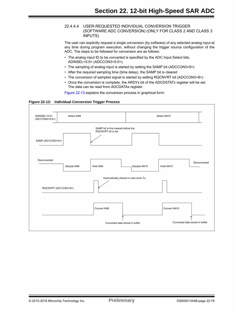
Section 22. 12-bit High-Speed SAR ADC
22.4.4.4 USER-REQUESTED INDIVIDUAL CONVERSION TRIGGER (SOFTWARE ADC CONVERSION) (ONLY FOR CLASS 2 AND CLASS 3 INPUTS)
The user can explicitly request a single conversion (by software) of any selected analog input atany time during program execution, without changing the trigger source configuration of theADC. The steps to be followed for conversion are as follows:
• The analog input ID to be converted is specified by the ADC Input Select bits, ADINSEL<5:0> (ADCCON3<5:0>).
• The sampling of analog input is started by setting the SAMP bit (ADCCON3<9>)
• After the required sampling time (time delay), the SAMP bit is cleared
• The conversion of sampled signal is started by setting RQCNVRT bit (ADCCON3<8>)
• Once the conversion is complete, the ARDYx bit of the ADCDSTATx register will be set. The data can be read from ADCDATAx register.
Figure 22-13 explains the conversion process in graphical form:
Figure 22-13: Individual Conversion Trigger Process
SAMP (AD1CON3<9>)
Hold AN8
Convert AN8
Select AN8ADINSEL<5:0> (AD1CON3<5:0>)
Sample AN8
Disconnected
RQCNVRT (AD1CON3<8>)
SAMP bit is first cleared before the RQCNVRT bit is set
Automatically cleared in next clock TQ
Converted data stored in buffer
Select AN10
Hold AN10Sample AN10
Convert AN10
Converted data stored in buffer
Disconnected
© 2015-2016 Microchip Technology Inc. Preliminary DS60001344B-page 22-79

PIC32 Family Reference Manual
22.4.5 Selecting the Voltage Reference Source
The user application can select the voltage reference for the ADC module, which can be internalor external. The Voltage Reference Input Selection bits, VREFSEL<2:0> (ADCCON3<15:13>),select the voltage reference for analog-to-digital conversions. The upper voltage reference(VREFH) and the lower voltage reference (VREFL) may be the internal AVDD and AVSS voltage railsor the band gap reference generator or the external VREF+ and VREF- input pins. When thevoltage reference and band gap reference are ready, the BGVRRDY (ADCCON2<31>) bit is set.If a Fault occurs in the voltage reference (such as a brown-out), the REFFLT bit(ADCCON2<30>) is set. The BGVRRDY and REFFLT bits can also generate interrupts if theBGVRIEN bit (ADCCON2<15>) and REFFLTIEN bit (ADCCON2<14>) are set, respectively.
The voltages applied to the external reference pins must comply with certain specifications. Referto the “Electrical Characteristics” chapter in the specific device data sheet for the electricalspecifications.
The Analog Input Charge Pump Enable bit, AICPMPEN (ADCCON1<12>), should be set whenthe difference between the selected reference voltages (VREFH - VREFL) is less than 0.65 * (AVDD
- AVSS). Setting this bit does not increase the magnitude of reference voltage; however, settingthis bit reduces the series source resistance to the sampling capacitors. This maximizes the SNRfor analog-to-digital conversions using small reference voltage rails.
22.4.6 Selecting the Scanned Inputs
All available analog inputs can be configured for scanning. Class 1 inputs are sampled using theirdedicated ADC module. Class 2 and Class 3 inputs are sampled using the shared ADC module.A single conversion trigger source is selected for all of the inputs selected for scanning using theSTRGSRC<4:0> bits (ADCCON1<20:16>). On each conversion trigger, the ADC module startsconverting in the natural priority all inputs specified in the user-specified scan list (ADCCSS1 orADCCSS2). For Class 1 inputs, sampling ends at the time of the trigger and conversion for all ofthem begin in parallel. For Class 2 and Class 3 inputs, the trigger initiates a sequentialsample/conversion process in the natural priority order.
An analog input belongs to the scan if it is:
• A Class 3 input. For Class 3 inputs, scan is the only mechanism for conversion.
• A Class 1 or a Class 2 input, which has the scan trigger selected as the trigger source, by selecting the STRIG option in the TRGSRCx<4:0> bits located in the ADCTRG1 through ADCTRG8 registers.
The trigger options available for scan are identical to those available for independent triggeringof Class 1 and Class 2 inputs. Any Class 1 or Class 2 inputs that are part of the scan must havethe STRIG option selected as their trigger source in the TRGSRCx<4:0> bits.
Note 1: The external VREF+ and VREF- pins can be shared with other analog peripherals. Refer to the “Pin Tables” section of the specific device data sheet for more information. In addition, the ANSELx bits for the VREF+ and VREF- pins must be set to Analog mode.
2: The Band Gap reference source is not available on all devices. Please refer to the specific device data sheet to determine availability of this feature.
Note 1: Since the clock divisor, resolution and sampling time for each dedicated ADCmodule (SELRES, ADCDIV, and SAMC<9:0> bits in the ADCxTIME register),and the shared ADC module (SELRES in the ADCCON1 register, ADCDIV andSAMC<9:0> bits in the ADCCON2 register) are handled through separateregisters, if a scan sequence is to be set involving both dedicated and sharedinputs, each of these registers must be initialized individually, even in scanmode.
2: The end-of-scan (EOS) is generated only if all Class 1 inputs have completed thescan, and the last shared input conversion has completed. Until both of these con-ditions are met, the scan sequence is still in effect. Therefore, the EOS Interrupt canbe used for any scan sequence, with any combination of input types.
DS60001344B-page 22-80 Preliminary © 2015-2016 Microchip Technology Inc.

Section 22. 12-bit High-Speed SAR ADC
Example 22-3: ADC Scanning Multiple Inputsint main(int argc, char** argv) {
int result[3];
/* Configure ADCCON1 */ADCCON1 = 0; // No ADCCON1 features are enabled including: Stop-in-Idle, turbo,
// CVD mode, Fractional mode and scan trigger source.ADCCON1bits.SELRES = 3; // ADC7 resolution is 12 bitsADCCON1bits.STRGSRC = 1; // Select scan trigger.
/* Configure ADCCON2 */ADCCON2bits.SAMC = 5; // ADC7 sampling time = 5 * TAD7ADCCON2bits.ADCDIV = 1; // ADC7 clock freq is half of control clock = TAD7
/* Initialize warm up time register */ADCANCON = 0;ADCANCONbits.WKUPCLKCNT = 5; // Wakeup exponent = 32 * TADx
/* Clock setting */ADCCON3bits.ADCSEL = 0; // Select input clock sourceADCCON3bits.CONCLKDIV = 1; // Control clock frequency is half of input clockADCCON3bits.VREFSEL = 0; // Select AVDD and AVSS as reference source
ADC0TIMEbits.ADCDIV = 1; // ADC0 clock frequency is half of control clock = TAD0ADC0TIMEbits.SAMC = 5; // ADC0 sampling time = 5 * TAD0ADC0TIMEbits.SELRES = 3; // ADC0 resolution is 12 bits
/* Select analog input for ADC modules, no presync trigger, not sync sampling */ADCTRGMODEbits.SH0ALT = 0; // ADC0 = AN0
/* Select ADC input mode */ADCIMCON1bits.SIGN0 = 0; // unsigned data formatADCIMCON1bits.DIFF0 = 0; // Single ended modeADCIMCON1bits.SIGN8 = 0; // unsigned data formatADCIMCON1bits.DIFF8 = 0; // Single ended modeADCIMCON1bits.SIGN40 = 0; // unsigned data formatADCIMCON1bits.DIFF40 = 0; // Single ended mode
/* Configure ADCGIRQENx */ADCGIRQEN1 = 0; // No interrupts are used.ADCGIRQEN2 = 0;
/* Configure ADCCSSx */ADCCSS1 = 0; // Clear all bitsADCCSS2 = 0;ADCCSS1bits.CSS0 = 1; // AN0 (Class 1) set for scanADCCSS1bits.CSS8 = 1; // AN8 (Class 2) set for scanADCCSS2bits.CSS40 = 1; // AN40 (Class 3) set for scan
/* Configure ADCCMPCONx */ADCCMPCON1 = 0; // No digital comparators are used. Setting the ADCCMPCONxADCCMPCON2 = 0; // register to '0' ensures that the comparator is disabled.ADCCMPCON3 = 0; // Other registers are ‘don't care’.ADCCMPCON4 = 0;ADCCMPCON5 = 0;ADCCMPCON6 = 0;
/* Configure ADCFLTRx */ADCFLTR1 = 0; // No oversampling filters are used.ADCFLTR2 = 0;ADCFLTR3 = 0;ADCFLTR4 = 0;ADCFLTR5 = 0;ADCFLTR6 = 0;
© 2015-2016 Microchip Technology Inc. Preliminary DS60001344B-page 22-81
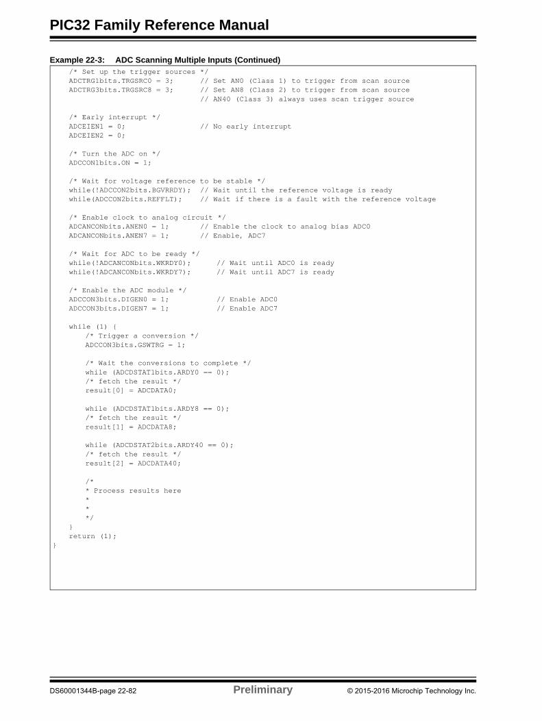
PIC32 Family Reference Manual
Example 22-3: ADC Scanning Multiple Inputs (Continued)/* Set up the trigger sources */ADCTRG1bits.TRGSRC0 = 3; // Set AN0 (Class 1) to trigger from scan sourceADCTRG3bits.TRGSRC8 = 3; // Set AN8 (Class 2) to trigger from scan source
// AN40 (Class 3) always uses scan trigger source
/* Early interrupt */ADCEIEN1 = 0; // No early interruptADCEIEN2 = 0;
/* Turn the ADC on */ADCCON1bits.ON = 1;
/* Wait for voltage reference to be stable */while(!ADCCON2bits.BGVRRDY); // Wait until the reference voltage is readywhile(ADCCON2bits.REFFLT); // Wait if there is a fault with the reference voltage
/* Enable clock to analog circuit */ADCANCONbits.ANEN0 = 1; // Enable the clock to analog bias ADC0ADCANCONbits.ANEN7 = 1; // Enable, ADC7
/* Wait for ADC to be ready */while(!ADCANCONbits.WKRDY0); // Wait until ADC0 is readywhile(!ADCANCONbits.WKRDY7); // Wait until ADC7 is ready
/* Enable the ADC module */ADCCON3bits.DIGEN0 = 1; // Enable ADC0ADCCON3bits.DIGEN7 = 1; // Enable ADC7
while (1) {/* Trigger a conversion */ADCCON3bits.GSWTRG = 1;
/* Wait the conversions to complete */while (ADCDSTAT1bits.ARDY0 == 0);/* fetch the result */result[0] = ADCDATA0;
while (ADCDSTAT1bits.ARDY8 == 0);/* fetch the result */result[1] = ADCDATA8;
while (ADCDSTAT2bits.ARDY40 == 0);/* fetch the result */result[2] = ADCDATA40;
/** Process results here***/
}return (1);
}
DS60001344B-page 22-82 Preliminary © 2015-2016 Microchip Technology Inc.
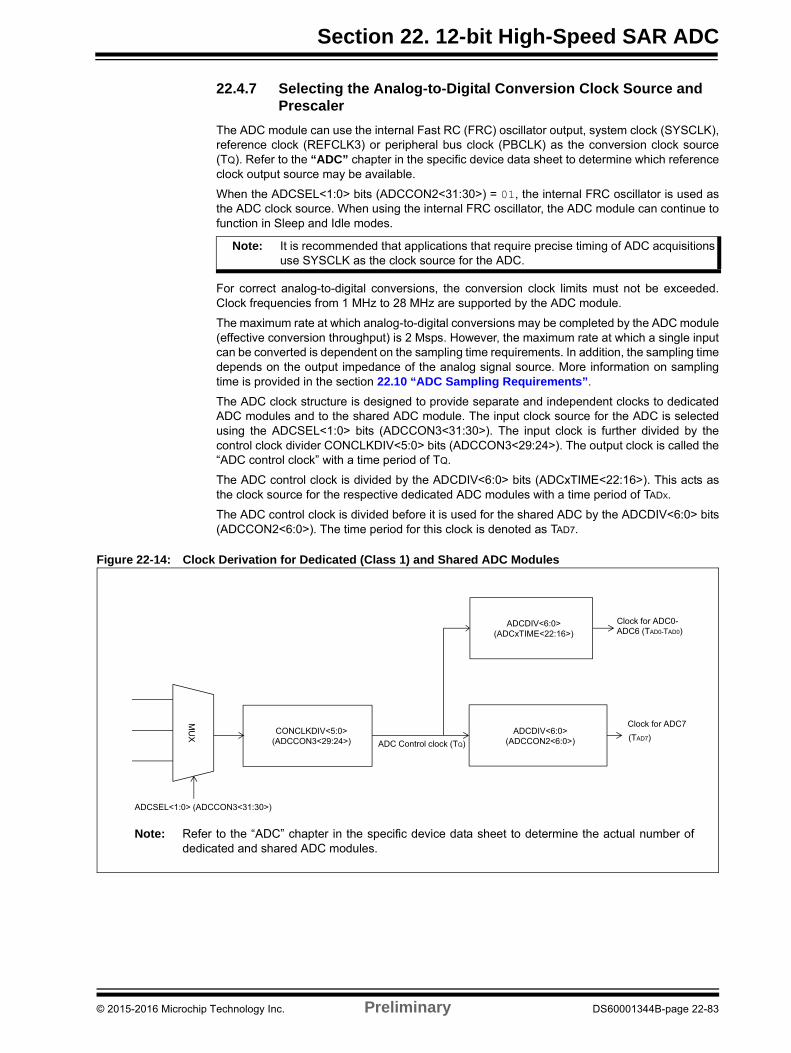
Section 22. 12-bit High-Speed SAR ADC
22.4.7 Selecting the Analog-to-Digital Conversion Clock Source and Prescaler
The ADC module can use the internal Fast RC (FRC) oscillator output, system clock (SYSCLK),reference clock (REFCLK3) or peripheral bus clock (PBCLK) as the conversion clock source(TQ). Refer to the “ADC” chapter in the specific device data sheet to determine which referenceclock output source may be available.
When the ADCSEL<1:0> bits (ADCCON2<31:30>) = 01, the internal FRC oscillator is used asthe ADC clock source. When using the internal FRC oscillator, the ADC module can continue tofunction in Sleep and Idle modes.
For correct analog-to-digital conversions, the conversion clock limits must not be exceeded.Clock frequencies from 1 MHz to 28 MHz are supported by the ADC module.
The maximum rate at which analog-to-digital conversions may be completed by the ADC module(effective conversion throughput) is 2 Msps. However, the maximum rate at which a single inputcan be converted is dependent on the sampling time requirements. In addition, the sampling timedepends on the output impedance of the analog signal source. More information on samplingtime is provided in the section 22.10 “ADC Sampling Requirements”.
The ADC clock structure is designed to provide separate and independent clocks to dedicatedADC modules and to the shared ADC module. The input clock source for the ADC is selectedusing the ADCSEL<1:0> bits (ADCCON3<31:30>). The input clock is further divided by thecontrol clock divider CONCLKDIV<5:0> bits (ADCCON3<29:24>). The output clock is called the“ADC control clock” with a time period of TQ.
The ADC control clock is divided by the ADCDIV<6:0> bits (ADCxTIME<22:16>). This acts asthe clock source for the respective dedicated ADC modules with a time period of TADX.
The ADC control clock is divided before it is used for the shared ADC by the ADCDIV<6:0> bits(ADCCON2<6:0>). The time period for this clock is denoted as TAD7.
Figure 22-14: Clock Derivation for Dedicated (Class 1) and Shared ADC Modules
Note: It is recommended that applications that require precise timing of ADC acquisitionsuse SYSCLK as the clock source for the ADC.
MU
X
ADCSEL<1:0> (AD CON3<31:30>)
CONCLKDIV<5:0>(AD CON3<29:24>)
ADCDIV<6:0>(AD CON2<6:0>)
Clock for (TAD )
ADCDIV<6:0>(AD TIME<22:16>)
Clock for(TAD
ADC Control clock (TQ)
Note: Refer to the “ADC” chapter in the specific device data sheet to determine the actual number ofdedicated and shared ADC modules.
© 2015-2016 Microchip Technology Inc. Preliminary DS60001344B-page 22-83

PIC32 Family Reference Manual
22.4.8 Sample and Conversion Time
Equation 22-1: Sample Time for Dedicated ADC Modules
Equation 22-2: Sample Time for the Shared ADC Module
22.4.9 Turning ON the ADC
Turning ON the ADC module involves these steps:
When the ADC module enable bit, ON (ADCCON1<15>), is set to ‘1’, the module is in Activemode and is fully powered and functional. When the ON bit is ‘0’, the ADC module is disabled.Once disabled, the digital and analog portions of the ADC are turned off for maximum currentsavings. In addition to setting the ON bit, the analog and digital circuits of ADC should be turnedON. More details are provided in the Section 22.7.3 “ADC Low-power Mode”.
22.4.10 ADC Status Bits
The ADC module includes the WKRDYx/WKRDY7 status bit in the ADCANCON register, whichindicates the current state of ADC Analog and bias circuit. The user application should notperform any ADC operations until this bit is set.
Note: Writing to the ADC control bits that control the ADC clock, input assignments,scanning, voltage reference selection, S&H circuit operating modes, and interruptconfiguration is not recommended while the ADC module is enabled.
tSAMC ADCxTIME<9:0> TAD=
tconversion 2 ADCxTIME<25:24>+ TAD=
tSAMC ADCCON2<25:16> TAD=
tconversion 2 ADCCON1<22:21>+ TAD=
DS60001344B-page 22-84 Preliminary © 2015-2016 Microchip Technology Inc.

Section 22. 12-bit High-Speed SAR ADC
22.4.11 On-the-fly Update of SFRs
Certain applications require updating the SFRs of dedicated and shared ADC modules withoutdisabling the ADC. While this is achievable with the ADC, the user code must follow certainguidelines to prevent data corruption. An update to an SFR has the potential of completelycorrupting the output data if the actual moment when the SFRs changes occurs towards the endof the sampling time of the ADC module.
Any ADC module can find itself in three possible states:
• Idle: During the Idle state, the ADC module waits for the next trigger event. This is not a safe time to change SFR settings as there is no way for the user code to predict when the next asynchronous trigger (which signals the end-of-sampling) will occur. If an end-of-sam-pling occurs while the SFRs are being modified, the output data will be corrupted.
• Sampling: No SFRs whatsoever should be changed while the ADC module is sampling for obvious analog reasons
• Converting: This is the safest time period to update the SFRs as the conversion time is fixed and under the control of the SAR itself
To update the SFRs while the ADC is converting, the Early interrupt Enable and Early InterruptStatus registers (see Register 22-37 through Register 22-40) can be used.
For example, if the ADCEIS<2:0> bit (ADCxTIME<28:26) is set to ‘0b111, at the time EIRDYxgoes high, the successive approximation of ADC module ‘x’ is performing step 6 (= 14 - 8) of theconversion. The user application can modify the SFRs for ADC module ‘x’ at this time, with theexception of changing the clock setting using the ADCSEL<1:0>, CONCLKDIV<5:0>,ADCDIV<6:0>, and ADCDIV<6:0> bits, provided all of the SFR writes are going to be ready bystep 13 of the SAR of ADC module ‘x’. This safe time for new SFR writes depends on the settingof the ADCDIV<6:0> bits. This is because, the write to SFR from software happens at systemclock frequency. When the value of ADCDIV<6:0> is high, which equates to a lower ADC speed,the write to the SFR will happen safely, as compared to when the value of ADCDIV<6:0> is low,which equates to a higher ADC speed. For high ADC speed, the user application can poll theEIRDYx bit instead of using the early interrupt. This is because the interrupt latency for servicingthe early ISR will take some cycles, which can be avoided in polled mode.
The following are a list of SFR bits that can be updated during the safe period:
• STRGSRC<4:0> (ADCCON1<20:16>) - see Register 22-1
• SAMC<7:0> (ADCCON2<23:16>) - see Register 22-2
• STRGENx (ADCTRGMODE<14:8) - see Register 22-4
• SSAMPENx (ADCTRGMODE<6:0>) - see Register 22-4
• SHxALT<1:0> (ADCTRGMODE<29:8>) - see Register 22-4
• DIFFx (ADCIMCONx) - see Register 22-5 through Register 22-8
• SIGNx (ADCIMCONx) - see Register 22-5 through Register 22-8
• CSS63:CSS0 (ADCCSS1<31:0>, ADCCSS2<63:32>) - see Register 22-11 and Register 22-12
• TRGSRCx<4:0> (ADCTRGx) - see Register 22-18
• LVL31:LVL0 (ADCTRGSNS<31:0>) - see Register 22-35
• SAMC<7:0> (ADCxTIME<7:0>) - see Register 22-36
In addition to using the early interrupts, the Trigger Suspend bit, TRGSUSP (ADCCON3<12>),can be used for writing new values to an SFR. The steps to use the TRGSUSP bit are as follows:
1. Set the TRGSUSP bit (ADCCON3<12>).
2. Poll for the UPDRDY bit (ADCCON3<10>) to be set. Optionally, an interrupt can begenerated by enabling the UPDIEN bit (ADCCON3<11>). Once the UPDRDY bit is set, itindicates that all triggers are suspended and all ADC modules are in their idle state.
3. Write new values to the SFR (except changing clock setting using the ADCSEL<1:0>,CONCLKDIV<5:0>, ADCDIV<6:0>, and ADCDIV<6:0> bits).
4. Clear the TRGSUSP bit to allow the ADC resume operations.
Updating SFRs related to clock setting of ADC using the ADCSEL<1:0>, CONCLKDIV<5:0>,ADCDIV<6:0>, and ADCDIV<6:0> bits can only be performed by disabling the ADC (ON bit(ADCCON1<15>) = 0).
© 2015-2016 Microchip Technology Inc. Preliminary DS60001344B-page 22-85

PIC32 Family Reference Manual
22.5 ADDITIONAL ADC FUNCTIONS
This section describes some additional features of the ADC module, which includes:
• Digital comparator
• Oversampling filter
• Turbo mode
• CVD mode
22.5.1 Digital Comparator
The ADC module features digital comparators that can be used to monitor selected analog inputconversion results and generate interrupts when a conversion result is within the user-specifiedlimits. Conversion triggers are still required to initiate conversions. The comparison occursautomatically once the conversion is complete. This feature is enabled by setting the DigitalComparator Module Enable bit, ENDCMP (ADCCMPCONx<7>).
The user application makes use of an interrupt that is generated when the analog-to-digitalconversion result is higher or lower than the specified high and low limit values in the ADCCMPxregister. The high and low limit values are specified in the DCMPHI<15:0> bits(ADCCMPx<31:16>) and the DCMPLO<15:0> bits (ADCCMPx<15:0>).
The CMPEx bits (‘x’ = 0 through 31) in the ADCCMPENx registers are used to specify whichanalog inputs are monitored by the digital comparator (for the first 32 analog inputs, ANx, where‘x’ = 0 through 31). The ADCCMPCONx register specifies the comparison conditions that willgenerate an interrupt, as follows:
• When IEBTWN = 1, interrupt is generated when DCMPLO ≤ ADCDATA < DCMPHI
• When IEHIHI = 1, interrupt is generated when DCMPHI ≤ ADCDATA
• When IEHILO = 1, interrupt is generated when ADCDATA < DCMPHI
• When IELOHI = 1, interrupt is generated when DCMPLO ≤ ADCDATA
• When IELOLO = 1, interrupt is generated when ADCDATA < DCMPLO
The comparator event generation is illustrated in Figure 22-15. When the ADC module generatesa conversion result, the conversion result is provided to the comparator. The comparator usesthe DIFFx and SIGNx bits of the ADCIMCONx register (depending on the analog input used) todetermine the data format used and appropriately select whether the comparison should besigned or unsigned. The global ADC setting, which is specified by the FRACT bit(ADCCON1<23>), is also used to set the fractional or integer format. The digital comparatorcompares the ADC result with the high and low limit values (depending on the selectedcomparison criteria) in the ADCCMPx register.
Depending on the comparator results, a digital comparator interrupt event may be generated. Ifa comparator event occurs, the Digital Comparator Interrupt Event Detected status bit, DCMPED(ADCCMPCONx<5>), is set, and the Analog Input Identification (ID) bits, AINID<4:0>(ADCCMPCONx<12:8>), are automatically updated so that the user application knows whichanalog input generated the interrupt event.
Note 1: The Digital Comparator module supports only the first 32 analog inputs(AN0 through AN31).
2: The user software must format the values contained in the ADCCMPx registers tomatch converted data format as either signed or unsigned, and fractional or integer.
DS60001344B-page 22-86 Preliminary © 2015-2016 Microchip Technology Inc.
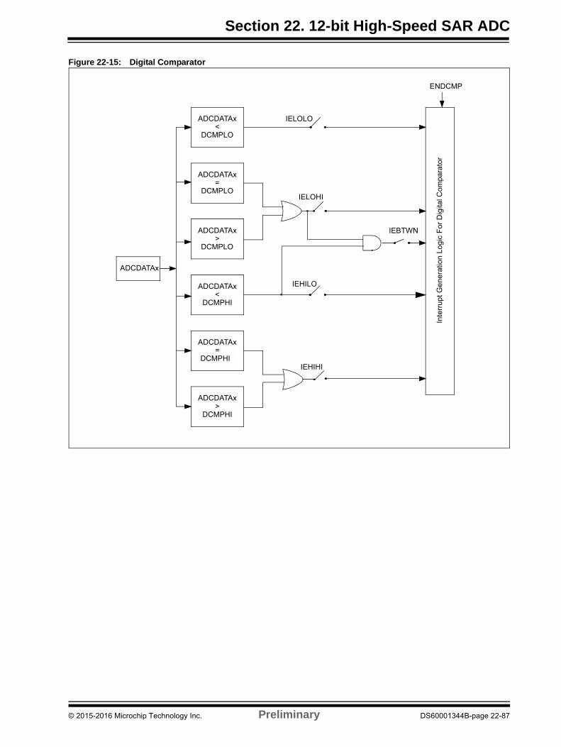
Section 22. 12-bit High-Speed SAR ADC
Figure 22-15: Digital Comparator
ADCDATAx<
DCMPLO
ADCDATAx=
DCMPLO
ADCDATAx>
DCMPLO
ADCDATAx<
DCMPHI
ADCDATAx=
DCMPHI
ADCDATAx>
DCMPHI
IELOLO
IELOHI
IEHILO
IEHIHI
IEBTWN
ENDCMP
Inte
rru
pt
Ge
ne
ratio
n L
og
ic F
or
Dig
ital C
om
para
tor
ADCDATAx
© 2015-2016 Microchip Technology Inc. Preliminary DS60001344B-page 22-87

PIC32 Family Reference Manual
Example 22-4: ADC Digital Comparatorint main(int argc, char** argv) {
int result = 0, eventFlag = 0;
/* Configure ADCCON1 */ADCCON1 = 0; // No ADCCON1 features are enabled including: Stop-in-Idle,
// turbo, CVD mode, Fractional mode and scan trigger source.ADCCON1bits.SELRES = 3; // ADC resolution is 12 bitsADCCON1bits.STRGSRC = 0; // No scan trigger.
/* Configure ADCCON2 */ADCCON2bits.SAMC = 5; // ADC7 sampling time = 5 * TAD7ADCCON2bits.ADCDIV = 1; // ADC7 clock freq = TAD7
/* Initialize warm up time register */ADCANCON = 0;ADCANCONbits.WKUPCLKCNT = 5; // Wakeup exponent = 32 * TADx
/* Clock setting */ADCCON3 = 0;ADCCON3bits.ADCSEL = 0; // Select input clock sourceADCCON3bits.CONCLKDIV = 1; // Control clock frequency is half of input clockADCCON3bits.VREFSEL = 0; // Select AVDD and AVSS as reference source
/* No selection for dedicated ADC modules, no presync trigger, not sync sampling */ADCTRGMODEbits = 0;
/* Select ADC input mode */ADCIMCON1bits.SIGN8 = 0; // unsigned data formatADCIMCON1bits.DIFF8 = 0; // Single ended mode
/* Configure ADCGIRQENx */ADCGIRQEN1 = 0; // No interrupts are usedADCGIRQEN2 = 0;
/* Configure ADCCSSx */ADCCSS1 = 0; // No scanning is usedADCCSS2 = 0;
/* Configure ADCCMPCONx */ADCCMP1 = 0; // Clear the registerADCCMP1bits.DCMPHI = 0xC00; // High limit is a 3072 result.ADCCMP1bits.DCMPLO = 0x500; // Low limit is a 1280 result.ADCCMPCON1bits.IEBTWN = 1; // Create an event when the measured result is
// >= low limits and < high limit.ADCCMPEN1 = 0; // Clear all enable bitsADCCMPEN1bits.CMPE8 = 1; // set the bit corresponding to AN8ADCCMPCON1bits.ENDCMP = 1; // enable comparatorADCCMPCON2 = 0;ADCCMPCON3 = 0;ADCCMPCON4 = 0;ADCCMPCON5 = 0;ADCCMPCON6 = 0;
/* Configure ADCFLTRx */ADCFLTR1 = 0; // No oversampling filters are used.ADCFLTR2 = 0;ADCFLTR3 = 0;ADCFLTR4 = 0;ADCFLTR5 = 0;ADCFLTR6 = 0;
DS60001344B-page 22-88 Preliminary © 2015-2016 Microchip Technology Inc.
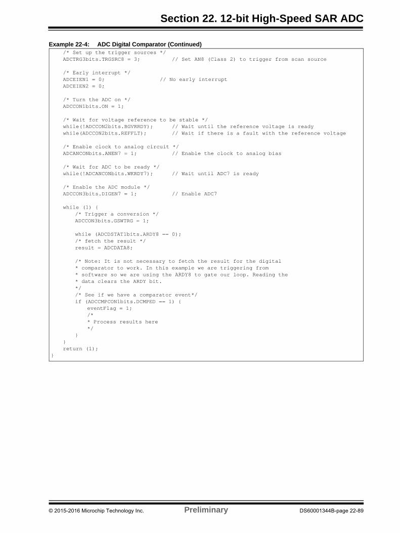
Section 22. 12-bit High-Speed SAR ADC
Example 22-4: ADC Digital Comparator (Continued)/* Set up the trigger sources */ADCTRG3bits.TRGSRC8 = 3; // Set AN8 (Class 2) to trigger from scan source
/* Early interrupt */ADCEIEN1 = 0; // No early interruptADCEIEN2 = 0;
/* Turn the ADC on */ADCCON1bits.ON = 1;
/* Wait for voltage reference to be stable */while(!ADCCON2bits.BGVRRDY); // Wait until the reference voltage is readywhile(ADCCON2bits.REFFLT); // Wait if there is a fault with the reference voltage
/* Enable clock to analog circuit */ADCANCONbits.ANEN7 = 1; // Enable the clock to analog bias
/* Wait for ADC to be ready */while(!ADCANCONbits.WKRDY7); // Wait until ADC7 is ready
/* Enable the ADC module */ADCCON3bits.DIGEN7 = 1; // Enable ADC7
while (1) {/* Trigger a conversion */ADCCON3bits.GSWTRG = 1;
while (ADCDSTAT1bits.ARDY8 == 0);/* fetch the result */result = ADCDATA8;
/* Note: It is not necessary to fetch the result for the digital* comparator to work. In this example we are triggering from* software so we are using the ARDY8 to gate our loop. Reading the* data clears the ARDY bit.*//* See if we have a comparator event*/if (ADCCMPCON1bits.DCMPED == 1) {
eventFlag = 1;/** Process results here*/
}}return (1);
}
© 2015-2016 Microchip Technology Inc. Preliminary DS60001344B-page 22-89
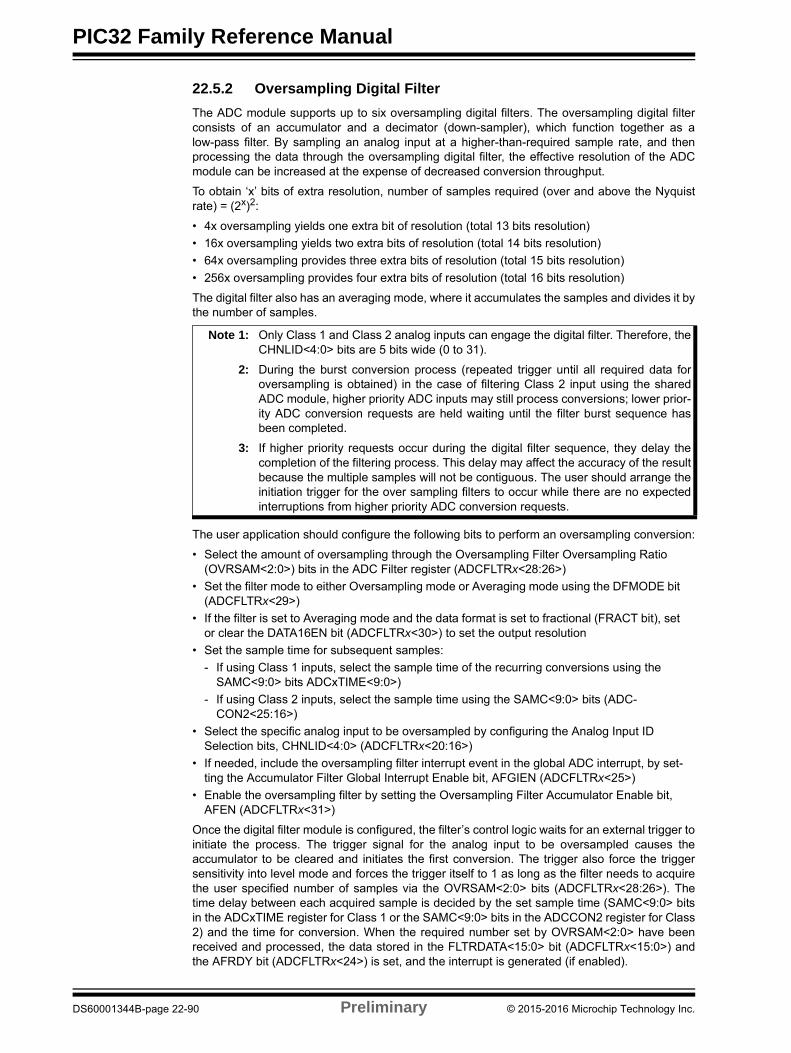
PIC32 Family Reference Manual
22.5.2 Oversampling Digital Filter
The ADC module supports up to six oversampling digital filters. The oversampling digital filterconsists of an accumulator and a decimator (down-sampler), which function together as alow-pass filter. By sampling an analog input at a higher-than-required sample rate, and thenprocessing the data through the oversampling digital filter, the effective resolution of the ADCmodule can be increased at the expense of decreased conversion throughput.
To obtain ‘x’ bits of extra resolution, number of samples required (over and above the Nyquistrate) = (2x)2:
• 4x oversampling yields one extra bit of resolution (total 13 bits resolution)
• 16x oversampling yields two extra bits of resolution (total 14 bits resolution)
• 64x oversampling provides three extra bits of resolution (total 15 bits resolution)
• 256x oversampling provides four extra bits of resolution (total 16 bits resolution)
The digital filter also has an averaging mode, where it accumulates the samples and divides it bythe number of samples.
The user application should configure the following bits to perform an oversampling conversion:
• Select the amount of oversampling through the Oversampling Filter Oversampling Ratio (OVRSAM<2:0>) bits in the ADC Filter register (ADCFLTRx<28:26>)
• Set the filter mode to either Oversampling mode or Averaging mode using the DFMODE bit (ADCFLTRx<29>)
• If the filter is set to Averaging mode and the data format is set to fractional (FRACT bit), set or clear the DATA16EN bit (ADCFLTRx<30>) to set the output resolution
• Set the sample time for subsequent samples:
- If using Class 1 inputs, select the sample time of the recurring conversions using the SAMC<9:0> bits ADCxTIME<9:0>)
- If using Class 2 inputs, select the sample time using the SAMC<9:0> bits (ADC-CON2<25:16>)
• Select the specific analog input to be oversampled by configuring the Analog Input ID Selection bits, CHNLID<4:0> (ADCFLTRx<20:16>)
• If needed, include the oversampling filter interrupt event in the global ADC interrupt, by set-ting the Accumulator Filter Global Interrupt Enable bit, AFGIEN (ADCFLTRx<25>)
• Enable the oversampling filter by setting the Oversampling Filter Accumulator Enable bit, AFEN (ADCFLTRx<31>)
Once the digital filter module is configured, the filter’s control logic waits for an external trigger toinitiate the process. The trigger signal for the analog input to be oversampled causes theaccumulator to be cleared and initiates the first conversion. The trigger also force the triggersensitivity into level mode and forces the trigger itself to 1 as long as the filter needs to acquirethe user specified number of samples via the OVRSAM<2:0> bits (ADCFLTRx<28:26>). Thetime delay between each acquired sample is decided by the set sample time (SAMC<9:0> bitsin the ADCxTIME register for Class 1 or the SAMC<9:0> bits in the ADCCON2 register for Class2) and the time for conversion. When the required number set by OVRSAM<2:0> have beenreceived and processed, the data stored in the FLTRDATA<15:0> bit (ADCFLTRx<15:0>) andthe AFRDY bit (ADCFLTRx<24>) is set, and the interrupt is generated (if enabled).
Note 1: Only Class 1 and Class 2 analog inputs can engage the digital filter. Therefore, theCHNLID<4:0> bits are 5 bits wide (0 to 31).
2: During the burst conversion process (repeated trigger until all required data foroversampling is obtained) in the case of filtering Class 2 input using the sharedADC module, higher priority ADC inputs may still process conversions; lower prior-ity ADC conversion requests are held waiting until the filter burst sequence hasbeen completed.
3: If higher priority requests occur during the digital filter sequence, they delay thecompletion of the filtering process. This delay may affect the accuracy of the resultbecause the multiple samples will not be contiguous. The user should arrange theinitiation trigger for the over sampling filters to occur while there are no expectedinterruptions from higher priority ADC conversion requests.
DS60001344B-page 22-90 Preliminary © 2015-2016 Microchip Technology Inc.
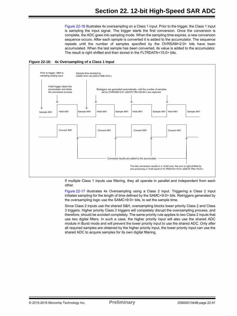
Section 22. 12-bit High-Speed SAR ADC
Figure 22-16 illustrates 4x oversampling on a Class 1 input. Prior to the trigger, the Class 1 inputis sampling the input signal. The trigger starts the first conversion. Once the conversion iscomplete, the ADC goes into sampling mode. When the sampling time expires, a new conversionsequence occurs. After each sample is converted it is added to the accumulator. The sequencerepeats until the number of samples specified by the OVRSAM<2:0> bits have beenaccumulated. When the last sample has been converted, its value is added to the accumulator.The result is right shifted and then stored in the FLTRDATA<15:0> bits.
Figure 22-16: 4x Oversampling of a Class 1 Input
If multiple Class 1 inputs use filtering, they all operate in parallel and independent from eachother.
Figure 22-17 illustrates 4x Oversampling using a Class 2 input. Triggering a Class 2 inputinitiates sampling for the length of time defined by the SAMC<9:0> bits. Retriggers generated bythe oversampling logic use the SAMC<9:0> bits, to set the sample time.
Since Class 2 inputs use the shared S&H, oversampling blocks lower priority Class 2 and Class3 triggers. Higher priority Class 2 triggers will completely disrupt the oversampling process, andtherefore, should be avoided completely. The same priority rule applies to two Class 2 inputs thatuse two digital filters. In such a case, the higher priority input will also use the shared ADCmodule in Burst mode and will prevent the lower priority input to use the shared ADC. Only afterall required samples are obtained by the higher priority input, the lower priority input can use theshared ADC to acquire samples for its own digital filtering.
Sample AN1 Hold AN1
Convert AN1
Prior to trigger, S&H is sampling analog input
Initial trigger clears the accumulator and starts the conversion process
Sample AN1 Hold AN1
Convert AN1
Sample AN1 Hold AN1
Convert AN1
Sample AN1 Hold AN1
Convert AN1
Converted results are added to the accumulator
Sample AN1
Sample time decided bySAMC<9:0> bit (AD TIME<9:0>)
The last conversion results in a 14-bit sum, the sum is right-shifted byone producing a 13-bit result in FLTRDATA<15:0> (AD FLTR <15:0>)
Retriggers are generated automatically, until the number of samples set by OVRSAM<2:0> (AD FLTRx<28:26>) are captured.
© 2015-2016 Microchip Technology Inc. Preliminary DS60001344B-page 22-91
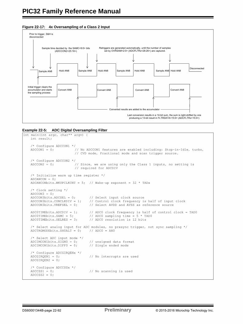
PIC32 Family Reference Manual
Figure 22-17: 4x Oversampling of a Class 2 Input
Example 22-5: ADC Digital Oversampling Filter
Sample AN8 Hold AN8
Convert AN8
Prior to trigger, S&H is disconnected
Initial trigger clears the accumulator and starts the sampling process
Sample AN8 Hold AN8
Convert AN8
Sample AN8 Hold AN8
Convert AN8
Sample AN8 Hold AN8
Convert AN8
Converted results are added to the accumulator
Sample time decided by the SAMC<9:0> bits(AD CON2<25:16>)
Last conversion results in a 14-bit sum, the sum is right-shifted by oneproducing a 13-bit result in FLTRDATA<15:0> (AD FLTR <15:0>)
Retriggers are generated automatically, until the number of samples set by OVRSAM<2:0> (AD FLTRx<28:26>) are captured.
Disconnected
int main(int argc, char** argv) {int result;
/* Configure ADCCON1 */ADCCON1 = 0; // No ADCCON1 features are enabled including: Stop-in-Idle, turbo,
// CVD mode, Fractional mode and scan trigger source.
/* Configure ADCCON2 */ADCCON2 = 0; // Since, we are using only the Class 1 inputs, no setting is
// required for ADCDIV
/* Initialize warm up time register */ADCANCON = 0;ADCANCONbits.WKUPCLKCNT = 5; // Wake-up exponent = 32 * TADx
/* Clock setting */ADCCON3 = 0;ADCCON3bits.ADCSEL = 0; // Select input clock sourceADCCON3bits.CONCLKDIV = 1; // Control clock frequency is half of input clockADCCON3bits.VREFSEL = 0; // Select AVDD and AVSS as reference source
ADC0TIMEbits.ADCDIV = 1; // ADC0 clock frequency is half of control clock = TAD0ADC0TIMEbits.SAMC = 5; // ADC0 sampling time = 5 * TAD0ADC0TIMEbits.SELRES = 3; // ADC0 resolution is 12 bits
/* Select analog input for ADC modules, no presync trigger, not sync sampling */ADCTRGMODEbits.SH0ALT = 0; // ADC0 = AN0
/* Select ADC input mode */ADCIMCON1bits.SIGN0 = 0; // unsigned data formatADCIMCON1bits.DIFF0 = 0; // Single ended mode
/* Configure ADCGIRQENx */ADCGIRQEN1 = 0; // No interrupts are usedADCGIRQEN2 = 0;
/* Configure ADCCSSx */ADCCSS1 = 0; // No scanning is usedADCCSS2 = 0;
DS60001344B-page 22-92 Preliminary © 2015-2016 Microchip Technology Inc.
Section 22. 12-bit High-Speed SAR ADC
Example 22-5: ADC Digital Oversampling Filter (Continued)/* Configure ADCCMPCONx */ADCCMPCON1 = 0; // No digital comparators are used. Setting the ADCCMPCONxADCCMPCON2 = 0; // register to '0' ensures that the comparator is disabled.ADCCMPCON3 = 0; // Other registers are ‘don't care’.ADCCMPCON4 = 0;ADCCMPCON5 = 0;ADCCMPCON6 = 0;
/* Configure ADCFLTRx */ADCFLTR1 = 0; // Clear all bitsADCFLTR1bits.CHNLID = 0; // Use AN0 as the sourceADCFLTR1bits.OVRSAM = 3; // 16x oversamplingADCFLTR1bits.DFMODE = 0; // Oversampling modeADCFLTR1bits.AFEN = 1; // Enable filter 1ADCFLTR2 = 0; // Clear all bitsADCFLTR3 = 0;ADCFLTR4 = 0;ADCFLTR5 = 0;ADCFLTR6 = 0;
/* Set up the trigger sources */ADCTGSNSbits.LVL0 = 0; // Edge triggerADCTRG1bits.TRGSRC0 = 1; // Set AN0 to trigger from software.
/* Turn the ADC on */ADCCON1bits.ON = 1;
/* Wait for voltage reference to be stable */while(!ADCCON2bits.BGVRRDY); // Wait until the reference voltage is readywhile(ADCCON2bits.REFFLT); // Wait if there is a fault with the reference voltage
/* Enable clock to analog circuit */ADCANCONbits.ANEN0 = 1; // Enable the clock to analog bias and digital control
/* Wait for ADC to be ready */while(!ADCANCONbits.WKRDY0); // Wait until ADC0 is ready
/* Enable the ADC module */ADCCON3bits.DIGEN0 = 1; // Enable ADC0
while (1) {/* Trigger a conversion */ADCCON3bits.GSWTRG = 1;
/* Wait for the oversampling process to complete */while (ADCFLTR1bits.AFRDY == 0);/* fetch the result */result = ADCFLTR1bits.FLTRDATA;
/** Process result Here** Note 1: Loop time determines the sampling time for the first sample.* remaining samples sample time is determined by set sampling + conversion time.** Note 2: The first 5 samples may have reduced accuracy.**/
}return (1);
}
© 2015-2016 Microchip Technology Inc. Preliminary DS60001344B-page 22-93
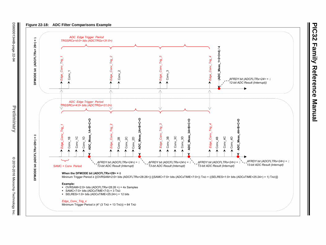
PIC
32 Fam
ily Referen
ce Ma
nu
al
DS
60
00
13
44
B-p
ag
e 2
2-9
4P
relimin
ary©
20
15
-20
16
Micro
chip
Te
chn
olo
gy In
c.
Con
v_4C
Con
v_4D
ADC
_Mea
s_4A
+B+C
+D
S<1:0> bits (ADCxTIME<25:24>) + 1) TAD)]}
LTRx<24>) = 1t (Interrupt)
AFRDY bit (ADCFLTRx<24>) = 113-bit ADC Result (Interrupt)
AFRDY bit (ADCFLTRx<24> = 112-bit ADC Result (Interrupt))
(AD
C_M
eas_
1+2+
3+4)
/ 4
Figure 22-18: ADC Filter Comparisons Example
Edg
e_C
onv_
Trig
_1
Edg
e_C
onv_
Trig
_2
Edg
e_C
onv_
Trig
_3
Edg
e_C
onv_
Trig
_4
ADC Edge Trigger PeriodTRGSRCx<4:0> bits (ADCTRGx<31:0>)
Edg
e_C
onv_
Trig
_1
Edg
e_C
onv_
Trig
_2
Edg
e_C
onv_
Trig
_3
Edg
e_C
onv_
Trig
_4
SAMC + Conv Period
ADC
_Mea
s_1A
+B+C
+D
Con
v_1B
Con
v_1C
Con
v_1D
Con
v_2B
Con
v_2C
Con
v_2D
Con
v_3B
Con
v_3C
Con
v_3D
Con
v_4B
ADC Edge Trigger PeriodTRGSRCx<4:0> bits (ADCTRGx<31:0>)
ADC
_Mea
s_2A
+B+C
+D
ADC
_Mea
s_3A
+B+C
+D
DFM
OD
E bi
t (A
DC
FLTR
x< 2
9>) =
1D
FMO
DE
bit (
ADC
FLTR
x<29
>) =
0
When the DFMODE bit (ADCFLTRx<29> = 0Mininum Trigger Period {(OVRSAM<2:0> bits (ADCFLTRx<28:26>)) [(SAMC<7:0> bits (ADCxTIME<7:0>)) TAD + ((SELRE
Example: OVRSAM<2:0> bits (ADCFLTRx<28:26 >) = 4x SamplesSAMC<7:0> bits (ADCxTIME<7:0) = 3 TADSELRES<1:0> bits (ADCxTIME<25:24>) = 12 bits
Edge_Conv_Trig_xMinimum Trigger Period (4* (3 TAD + 13 TAD)) = 64 TAD
AFRDY bit (ADCFLTRx<24>) = 113-bit ADC Result (Interrupt)
AFRDY bit (ADCFLTRx<24>) = 113-bit ADC Result (Interrupt)
AFRDY bit (ADCF13-bit ADC Resul
Con
v_1
Con
v_2
Con
v_3
Section 22. 12-bit High-Speed SAR ADC
22.5.3 FIFO Data Output
The dedicated ADC module has a provision to store the output data into a FIFO. This could beuseful while the ADC is used to convert signals at a very high throughput. The ADCFIFO registeris the read port for the FIFO. The FIFO is 128 level deep and is circular in nature.
The ADC module that needs to use the FIFO is selected by the ADCxEN bits(ADCFSTAT<30:24>). If more than one ADC module needs to use FIFO, all those respective bitscan be set among ADCxEN. While reading the data from FIFO, the ADCID<2:0> bits(ADCFSTAT<2:0>) should be read first and then the data from the ADCFIFO register. This way,the user application knows from which ADC module the data originated from the FIFO. The FENbit (ADCFSTAT<31>) bit is set to enable the FIFO operation. Once data is available in FIFO, theFRDY bit (ADCFSTAT<22>) is set and remains set until the FIFO is entirely read and is devoidof any data. If required, the FIEN bit (ADCFSTAT<23) can be set to generate interrupt.
Example 22-6: ADC FIFO Usage for Class 1 Input
Note 1: FIFO depth depends on the device. Please refer to the specific device data sheetfor details.
2: While retrieving data from the FIFO, user code should read both the ADCID<2:0>bits and the ADCFIFO register during each successive reads.
int main(int argc, char** argv) {int result[128], index = 0;
/* Configure ADCCON1 */ADCCON1 = 0; // No ADCCON1 features are enabled including: Stop-in-Idle, turbo,
// CVD mode, Fractional mode and scan trigger source.
/* Configure ADCCON2 */ADCCON2 = 0; // Since, we are using only the Class 1 inputs, no setting is
// required for ADCDIV
/* Initialize warm up time register */ADCANCON = 0;ADCANCONbits.WKUPCLKCNT = 5; // Wakeup exponent = 32 * TADx
/* Clock setting */ADCCON3 = 0;ADCCON3bits.ADCSEL = 0; // Select input clock sourceADCCON3bits.CONCLKDIV = 1; // Control clock frequency is half of input clockADCCON3bits.VREFSEL = 0; // Select AVDD and AVSS as reference source
ADC0TIMEbits.ADCDIV = 1; // ADC0 clock frequency is half of control clock = TAD0ADC0TIMEbits.SAMC = 5; // ADC0 sampling time = 5 * TAD0ADC0TIMEbits.SELRES = 3; // ADC0 resolution is 12 bits
/* Select analog input for ADC modules, no presync trigger, not sync sampling */ADCTRGMODEbits.SH0ALT = 0; // ADC0 = AN0
/* Select ADC input mode */ADCIMCON1bits.SIGN0 = 0; // unsigned data formatADCIMCON1bits.DIFF0 = 0; // Single ended mode
/* Configure ADCGIRQENx */ADCGIRQEN1 = 0; // No interrupts are usedADCGIRQEN2 = 0;
/* Configure ADCCSSx */ADCCSS1 = 0; // No scanning is usedADCCSS2 = 0;
/* Configure ADCCMPCONx */ADCCMPCON1 = 0; // No digital comparators are used. Setting the ADCCMPCONxADCCMPCON2 = 0; // register to '0' ensures that the comparator is disabled.ADCCMPCON3 = 0; // Other registers are ‘don't care’.ADCCMPCON4 = 0;ADCCMPCON5 = 0;ADCCMPCON6 = 0;
© 2015-2016 Microchip Technology Inc. Preliminary DS60001344B-page 22-95
PIC32 Family Reference Manual
Example 22-6: ADC FIFO Usage for Class 1 Input (Continued)/* Configure ADCFLTRx */ADCFLTR1 = 0; // Clear all bitsADCFLTR2 = 0;ADCFLTR3 = 0;ADCFLTR4 = 0;ADCFLTR5 = 0;ADCFLTR6 = 0;
/* Set up the trigger sources */ADCTGSNSbits.LVL0 = 0; // Edge triggerADCTRG0bits.TRGSRC0 = 1; // Set AN0 to trigger from software.
/* Early interrupt */ADCEIEN1 = 0; // No early interruptADCEIEN2 = 0;
/* Set FIFO */ADCFSTAT = 0; // Clear all bitsADCFSATbits.ADC0EN = 1; // Select ADC0ADCFSATbits.FEN = 1; // Enable FIFO
/* Turn the ADC on */ADCCON1bits.ON = 1;
/* Wait for voltage reference to be stable */while(!ADCCON2bits.BGVRRDY); // Wait until the reference voltage is readywhile(ADCCON2bits.REFFLT); // Wait if there is a fault with the reference voltage
/* Enable clock to analog circuit */ADCANCONbits.ANEN0 = 1; // Enable the clock to analog bias and digital control
/* Wait for ADC to be ready */while(!ADCANCONbits.WKRDY0); // Wait until ADC0 is ready
/* Enable the ADC module */ADCCON3bits.DIGEN0 = 1; // Enable ADC0
while (1) {/* Trigger a conversion */ADCCON3bits.GSWTRG = 1;
/* Wait the conversions to complete and data available in FIFO */while (ADCFSTATbits.FRDY == 0);
/* Once FIFO bit is set, read all possible data, until bit is clear */while(ADCFSTATbits.FRDY){
/* If data overflow occurred in FIFO, break read process */if(ADCFSTATbits.FWROVERR){
break;}/* if ADC ID is really '0', read data.This is more appropriate when multiple ADC modules areusing the FIFO, therefore, reading the ADC ID willidentify the ADC and data relation */if(ADCFSTATbits.ADCID == 0){
/* Read data from FIFO */result[index] = ADCFIFO;/* For each FIFO read, ADCFSTATbits.FCNT will keep reducing */index++;if(index >= 128)index = 0;
}}/** Process results here**/
}return (1);
}
DS60001344B-page 22-96 Preliminary © 2015-2016 Microchip Technology Inc.

Section 22. 12-bit High-Speed SAR ADC
22.5.4 Dedicated DMA-based Data Output
Depending on the device, each dedicated ADC module has a DMA engine that can be used tostore converted data directly into system memory (RAM). Refer to the “ADC” chapter in thespecific device data sheet to determine whether this feature is available for your device.
If the DMACNTEN bit in the ADCDMASTAT register is set, the ADC module current sample countis also written by the DMA engine into system RAM starting at the address specified in theADCCNTB register.
The size of the buffer used for storage is specified by the DMABL<2:0> bits(ADCCON1<2:0>). Also, the RAM address where the output data should be stored isspecified by the DMABADDR<31:0> bits in the ADCDMAB register. Each dedicated ADCmodule has two buffers: Buffer A and Buffer B.
Since DMABL<2:0> counts the number of data and each data is 16 bits, the actual size of thebuffer (in bytes) for each ADC module is given by the formula:
= 2(ADCCON1bits.DMABL + 1)
The channel storage buffers spaces are contiguous in the System RAM, starting at the baseaddress (given by the ADCDMAB register) with the ADC0 Buffer A, followed by the ADC0Buffer B, followed by the ADC1 Buffer A, followed by the ADC1 Buffer B, and so on in the naturalorder of the channel number assignments.
Table 22-6: DMA Buffer Format When Used by Multiple ADC Modules
As shown in Table 22-6, the user can get up to 128 samples (two bytes per sample) for each ADCmodule until data loss occurs by new data overwriting old data. The DMA engine will wrap aroundthe address for each channel inside its own allocated RAM space.
ADCx, ‘x’ = 0 through 6, will have Buffer A starting at:
= ADCDMAB + (2 * x) * 2(ADCCON1bits.DMABL + 1)
ADCx, ‘x’ = 0 through 6, will have Buffer B starting at:
= ADCDMAB + (2 * (x + 1)) * 2(ADCCON1bits.DMABL + 1)
The ADCCNTB register contains the user-given address at which (if the DMACNTEN bit(ADCDMASTAT<15>) is set) the DMA engine will start saving the current count of outputsamples already written to each of the buffers in the System RAM for each ADC module. TheADCx will have its Buffer A current sample count saved at the address ((ADCCNTB) + 2 * x) andits Buffer B current sample count saved at the address ((ADCCNTB) + (2 * x + 1)). Each ADCbuffer count takes only 1 byte of RAM storage, because the maximum value is 128. At any time,by reading the memory location specified by ADCCNTB register, the user can know the numberof available data for each ADC (0 through 6) and each buffer (A, B); even before the RAFx orRBFx bit is set.
ADC Module ID
Buffer RAM Address Space
0 A (DMABADDR<31:0>) + 0 to (DMABADDR<31:0>) + 255
0 B (DMABADDR<31:0>) + 256 to (DMABADDR<31:0>) + 511
1 A (DMABADDR<31:0>) + 512 to (DMABADDR<31:0>) + 767
1 B (DMABADDR<31:0>) + 768 to (DMABADDR<31:0>) + 1023
2 A (DMABADDR<31:0>) + 1024 to (DMABADDR<31:0>) + 1279
2 B (DMABADDR<31:0>) + 1280 to (DMABADDR<31:0>) + 1535
•••
•••
•••
6 A (DMABADDR<31:0>) + 3072 to (DMABADDR<31:0>) + 3327
6 B (DMABADDR<31:0>) + 3328 to (DMABADDR<31:0>) + 3583
© 2015-2016 Microchip Technology Inc. Preliminary DS60001344B-page 22-97
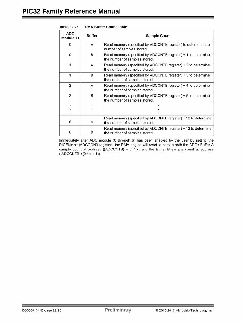
PIC32 Family Reference Manual
Table 22-7: DMA Buffer Count Table
Immediately after ADC module (0 through 6) has been enabled by the user by setting theDIGENx bit (ADCCON3 register), the DMA engine will reset to zero in both the ADCx Buffer Asample count at address ((ADCCNTB) + 2 * x) and the Buffer B sample count at address((ADCCNTB)+(2 * x + 1)).
ADC Module ID
Buffer Sample Count
0 A Read memory (specified by ADCCNTB register) to determine the number of samples stored.
0 B Read memory (specified by ADCCNTB register) + 1 to determine the number of samples stored.
1 A Read memory (specified by ADCCNTB register) + 2 to determine the number of samples stored.
1 B Read memory (specified by ADCCNTB register) + 3 to determine the number of samples stored.
2 A Read memory (specified by ADCCNTB register) + 4 to determine the number of samples stored.
2 B Read memory (specified by ADCCNTB register) + 5 to determine the number of samples stored.
•••
•••
•••
6 ARead memory (specified by ADCCNTB register) + 12 to determine the number of samples stored.
6 BRead memory (specified by ADCCNTB register) + 13 to determine the number of samples stored.
DS60001344B-page 22-98 Preliminary © 2015-2016 Microchip Technology Inc.

Section 22. 12-bit High-Speed SAR ADC
22.5.4.1 DMA PING-PONG MODE
The DMA engine Ping-Pong mode of operation when used with a single ADC module, isdescribed in the following steps:
1. DMA engine saves converted data into a buffer in system RAM for Buffer A.
2. Once Buffer A is full, the RAFx bit (ADCDMASTAT<6:0>) for the used ADC is set. Also,the DMA engine will start using and saving data into Buffer B.
3. An interrupt will be generated if the RAFIENx bit (ADCDMASTAT<14:8>) is set for theselected ADC.
4. Inside the ISR, the user application must know the buffer ID (either A or B) by reading theRAFx or RBFx bits.
5. Whichever bit is set, the user application must read the converted data from the buffer IDand perform suitable processing on the converted data.
6. While the user application is processing the converted data, the DMA engine is savingdata into Buffer B.
7. Once the user application completes the processing of data from Buffer A, it waits forcompletion of Buffer B.
If an application needs to use the data being stored in a buffer before the buffer is full, thefollowing steps are necessary:
1. To locate the data being saved in buffer, the user code should have enabled DMACNTENbit (ADCDMASTAT<15> register).
2. The current sample count can be retrieved from (ADCCNTB + (2 * x + 1)) (consideringBuffer B being used), and then read the suitable memory offset specified in the ADCDMABregister.
3. Once Buffer B is full, the RBFx bit for the used channel is set. Also, the DMA engine willstart saving data into Buffer A.
Figure 22-19 illustrates Ping-Pong mode with continuous operation.
Note 1: The initialization of the buffer sample count table to all zeros before enabling theDMA engine is left completely as a task for the software. It should be done in orderto avoid garbage data in the buffer sample count table before the first sample isbeing saved in each of the buffers.
2: A read of the ADCDMASTAT register will clear all status bits in this register.Because the dedicated ADC modules work completely independent one of another,more than one status bit can be set at the same time. The user must read theADCDMASTAT register and save its contents into a separate variable for logicbit-level operations to identify which dedicated ADC module buffers are full at thattime.
© 2015-2016 Microchip Technology Inc. Preliminary DS60001344B-page 22-99
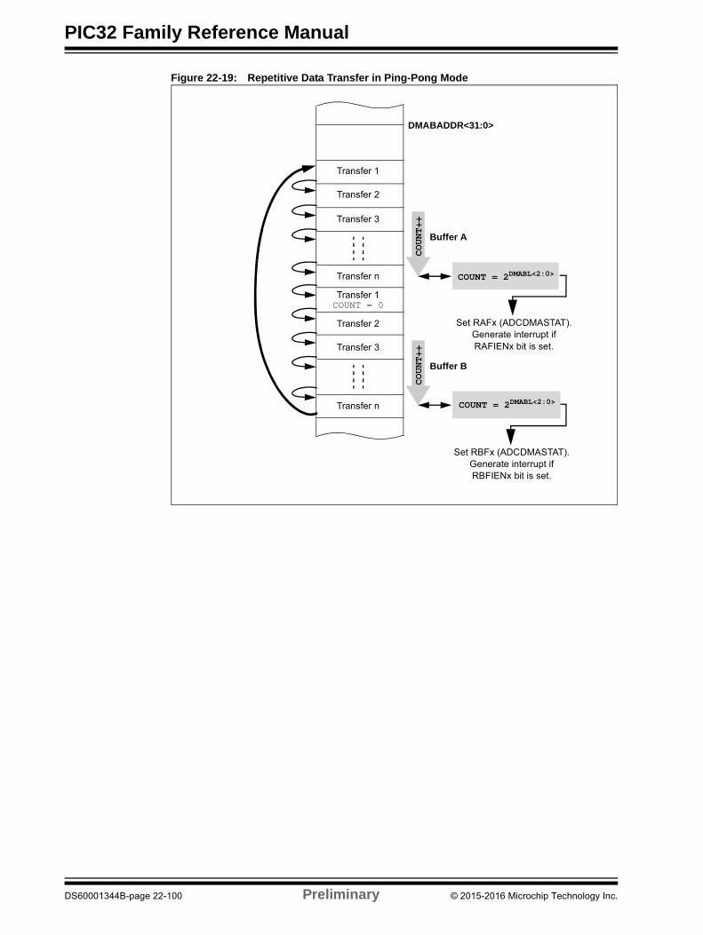
PIC32 Family Reference Manual
Figure 22-19: Repetitive Data Transfer in Ping-Pong Mode
DMABADDR<31:0>
Transfer 1
Transfer 2
Transfer 3
Transfer n
COUNT++
COUNT = 0
Set RAFx (ADCDMASTAT).Generate interrupt ifRAFIENx bit is set.
Transfer 1
Transfer 2
Transfer 3
Transfer nCOUNT++
Buffer A
Buffer B
COUNT = 2DMABL<2:0>
COUNT = 2DMABL<2:0>
Set RBFx (ADCDMASTAT).Generate interrupt if RBFIENx bit is set.
DS60001344B-page 22-100 Preliminary © 2015-2016 Microchip Technology Inc.
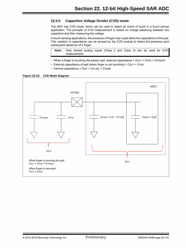
Section 22. 12-bit High-Speed SAR ADC
22.5.5 Capacitive Voltage Divider (CVD) mode
The ADC has CVD mode, which can be used to detect an event of touch in a touch sensorapplication. The principle of CVD measurement is based on charge balancing between twocapacitors and then measuring the voltage.
In touch sensing applications, the presence of finger near a pad alters the capacitance of the pad.This variation in capacitance can be sensed by the CVD module to detect the presence (andsubsequent absence) of a finger.
• When a finger is touching the sensor pad, external capacitance = CEXT = CPAD + CFINGER
• External capacitance of pad (when finger is not touching) = CEXT = CPAD
• Internal capacitance = CINT = CPLINE + CSAMP
Figure 22-20: CVD Mode Diagram
Note: Only shared analog inputs (Class 2 and Class 3) can be used for CVDmeasurement.
I/O Pad
CFINGER CPAD CPLINE = 2.5…17.5 pF CSAMP = 5 pF
When finger is touching the pad:CEXT = CPAD + CFINGER
When finger is removed:CEXT = CPAD
CINT
CEXT
© 2015-2016 Microchip Technology Inc. Preliminary DS60001344B-page 22-101
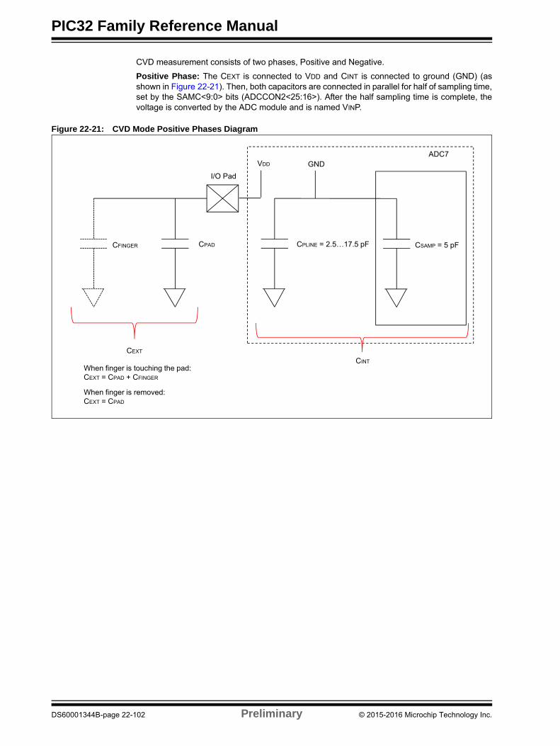
PIC32 Family Reference Manual
CVD measurement consists of two phases, Positive and Negative.
Positive Phase: The CEXT is connected to VDD and CINT is connected to ground (GND) (asshown in Figure 22-21). Then, both capacitors are connected in parallel for half of sampling time,set by the SAMC<9:0> bits (ADCCON2<25:16>). After the half sampling time is complete, thevoltage is converted by the ADC module and is named VINP.
Figure 22-21: CVD Mode Positive Phases Diagram
I/O Pad
CFINGER CPAD CPLINE = 2.5…17.5 pF CSAMP = 5 pF
When finger is touching the pad:CEXT = CPAD + CFINGER
When finger is removed:CEXT = CPAD
CINT
CEXT
VDD GND
DS60001344B-page 22-102 Preliminary © 2015-2016 Microchip Technology Inc.
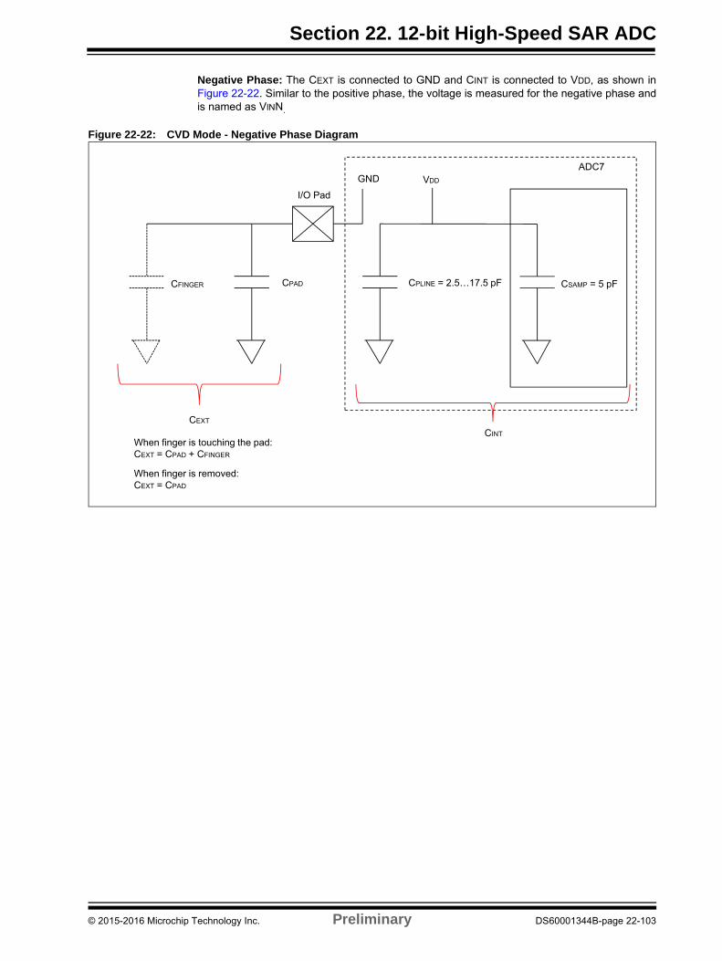
Section 22. 12-bit High-Speed SAR ADC
Negative Phase: The CEXT is connected to GND and CINT is connected to VDD, as shown inFigure 22-22. Similar to the positive phase, the voltage is measured for the negative phase andis named as VINN.
Figure 22-22: CVD Mode - Negative Phase Diagram
I/O Pad
CFINGER CPAD CPLINE = 2.5…17.5 pF CSAMP = 5 pF
When finger is touching the pad:CEXT = CPAD + CFINGER
When finger is removed:CEXT = CPAD
CINT
CEXT
GND VDD
© 2015-2016 Microchip Technology Inc. Preliminary DS60001344B-page 22-103
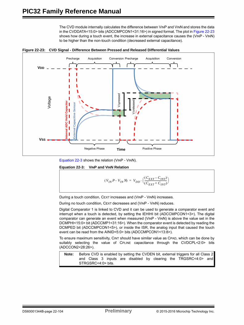
PIC32 Family Reference Manual
The CVD module internally calculates the difference between VINP and VINN and stores the datain the CVDDATA<15:0> bits (ADCCMPCON1<31:16>) in signed format. The plot in Figure 22-23shows how during a touch event, the increase in external capacitance causes the (VINP - VINN)to be higher than the non-touch condition (decreased external capacitance).
Figure 22-23: CVD Signal - Difference Between Pressed and Released Differential Values
Equation 22-3 shows the relation (VINP - VINN).
Equation 22-3: VINP and VINN Relation
During a touch condition, CEXT increases and (VINP - VINN) increases.
During no touch condition, CEXT decreases and (VINP - VINN) reduces.
Digital Comparator 1 is linked to CVD and it can be used to generate a comparator event andinterrupt when a touch is detected, by setting the IEHIHI bit (ADCCMPCON1<3>). The digitalcomparator can generate an event when measured (VINP - VINN) is above the value set in theDCMPHI<15:0> bit (ADCCMP1<31:16>). When the comparator event is detected by reading theDCMPED bit (ADCCMPCON1<5>), or inside the ISR, the analog input that caused the touchevent can be read from the AINID<5:0> bits (ADCCMPCON1<13:8>).
To ensure maximum sensitivity, CINT should have similar value as CPAD, which can be done bysuitably selecting the value of CPLINE capacitance through the CVDCPL<2:0> bits(ADCCON2<28:26>).
VDD
VSS
TimeNegative Phase Positive Phase
Precharge Acquisition Conversion Precharge Acquisition Conversion
Vo
ltag
e
Inte
rnal
AD
C H
old
Ca
pac
ito
r
Ex
tern
al C
apac
itiv
e S
en
so
r
Vr
elea
sed
V
pres
sed
Note: Before CVD is enabled by setting the CVDEN bit, external triggers for all Class 2and Class 3 inputs are disabled by clearing the TRGSRC<4:0> andSTRGSRC<4:0> bits.
VIN P VIN N– VDD
CEXT CINT– CEXT CINT+
------------------------------------ =
DS60001344B-page 22-104 Preliminary © 2015-2016 Microchip Technology Inc.

Section 22. 12-bit High-Speed SAR ADC
Example 22-7: ADC CVD Modeunsigned char touchDetected = 0;
void __ISR(_ADC_DC1_VECTOR, IPL3AUTO) _IntHandlerDrvAdc(void){ IFS1bits.ADCDC1IF = 0;
/* Check and clear event flag for comparator 1 */ if(ADCCMPCON1bits.DCMPED == 1) {
/* Verify if comparator event really due to AN21 */ if(ADCCMPCON1bits.AINID == 21) { touchDetected = 1; } }}
int main(void){
/* Configure ADCCON1 */ ADCCON1bits.SELRES = 3; // ADC resolution is 12 bits ADCCON1bits.STRGSRC = 0; // No scan trigger. ADCCON1bits.AICPMPEN = 0; ADCCON1bits.FRACT = 0; // Integer format
/* Configure ADCCON2 */ ADCCON2bits.SAMC = 32; // ADC7 sampling time ADCCON2bits.ADCDIV = 4; // ADC7 clock freq is half of control clock = TAD7 ADCCON2bits.CVDCPL = 2; // 5 pF is the CVD capacitor value selected
/* Initialize warm up time register */ ADCANCON = 0; ADCANCONbits.WKUPCLKCNT = 5; // Wakeup exponent = 32 * TADx
/* Clock setting */ ADCCON3 = 0; ADCCON3bits.ADCSEL = 0; // Select input clock source ADCCON3bits.CONCLKDIV = 1; // Control clock frequency is half of input clock ADCCON3bits.VREFSEL = 0; // Select AVDD and AVSS as reference source
/* No selection for dedicated ADC modules, no presync trigger, not sync sampling */ ADCTRGMODE = 0; /* Select ADC input mode */ ADCIMCON2bits.SIGN21 = 1; // signed data format ADCIMCON2bits.DIFF21 = 0; // Single ended mode
/* Configure ADCGIRQENx */ ADCGIRQEN1 = 0; // No interrupts are used. ADCGIRQEN2 = 0;
/* Configure ADCCSSx */ ADCCSS1 = 0; // No scanning is used ADCCSS2 = 0; ADCCSS1bits.CSS21 = 1; // AN21 (Class 3) set for CVD
/* Configure ADCCMPCONx */ ADCCMP1 = 0; // Clear the register ADCCMP1bits.DCMPHI = 1600; // High limit, depends on touch pad layout and selected
// cap, sample time etc. ADCCMP1bits.DCMPLO = 0; // Low limit, not very important for sensing touch event ADCCMPCON1bits.IEHIHI = 1; // When touched, the CVDDATA > HI_LIMIT(DCMPHI)
© 2015-2016 Microchip Technology Inc. Preliminary DS60001344B-page 22-105

PIC32 Family Reference Manual
Example 22-7: ADC CVD Mode (Continued)ADCCMPCON1bits.IEBTWN = 0;
ADCCMPCON1bits.IEHILO = 0; ADCCMPCON1bits.IELOHI = 0; ADCCMPCON1bits.IELOLO = 0; ADCCMPCON1bits.DCMPGIEN = 1; // enable interrupt ADCCMPCON1bits.ENDCMP = 1; // enable comparator ADCCMPEN1 = 0; // Clear all enable bits, as it is irrelevant in CVD mode ADCCMPCON2 = 0; ADCCMPCON3 = 0; ADCCMPCON4 = 0; ADCCMPCON5 = 0; ADCCMPCON6 = 0;
/* Configure ADCFLTRx */ ADCFLTR1 = 0; // No oversampling filters are used. ADCFLTR2 = 0; ADCFLTR3 = 0; ADCFLTR4 = 0; ADCFLTR5 = 0; ADCFLTR6 = 0;
/* Set up the trigger sources */ ADCTRGSNS = 0; ADCTRG1 = 0; ADCTRG2 = 0; ADCTRG3 = 0; /* Early interrupt */ ADCEIEN1 = 0; // No early interrupt ADCEIEN2 = 0;
/* Turn the ADC on */ ADCCON1bits.ON = 1; /* Wait for voltage reference to be stable */ while(!ADCCON2bits.BGVRRDY); // Wait until the reference voltage is ready while(ADCCON2bits.REFFLT); // Wait if there is a fault with the reference voltage /* Enable clock to analog circuit */ ADCANCONbits.ANEN7 = 1; // Enable the clock to analog bias /* Wait for ADC to be ready */ while(!ADCANCONbits.WKRDY7); // Wait until the ADC7 is ready
/* Enable interrupt setting for digital comparator 1 */ IFS1bits.ADCDC1IF = 0; IEC1bits.ADCDC1IE = 1; IPC11bits.ADCDC1IP = 3; IPC11bits.ADCDC1IS = 3; INTCONbits.MVEC = 1; __builtin_enable_interrupts();
/* Enable the ADC module */ADCCON3bits.DIGEN7 = 1; // Enable ADC7
/* Turn the CVD mode on */ADCCON1bits.CVDEN = 1;while (1);
return (1);}
DS60001344B-page 22-106 Preliminary © 2015-2016 Microchip Technology Inc.
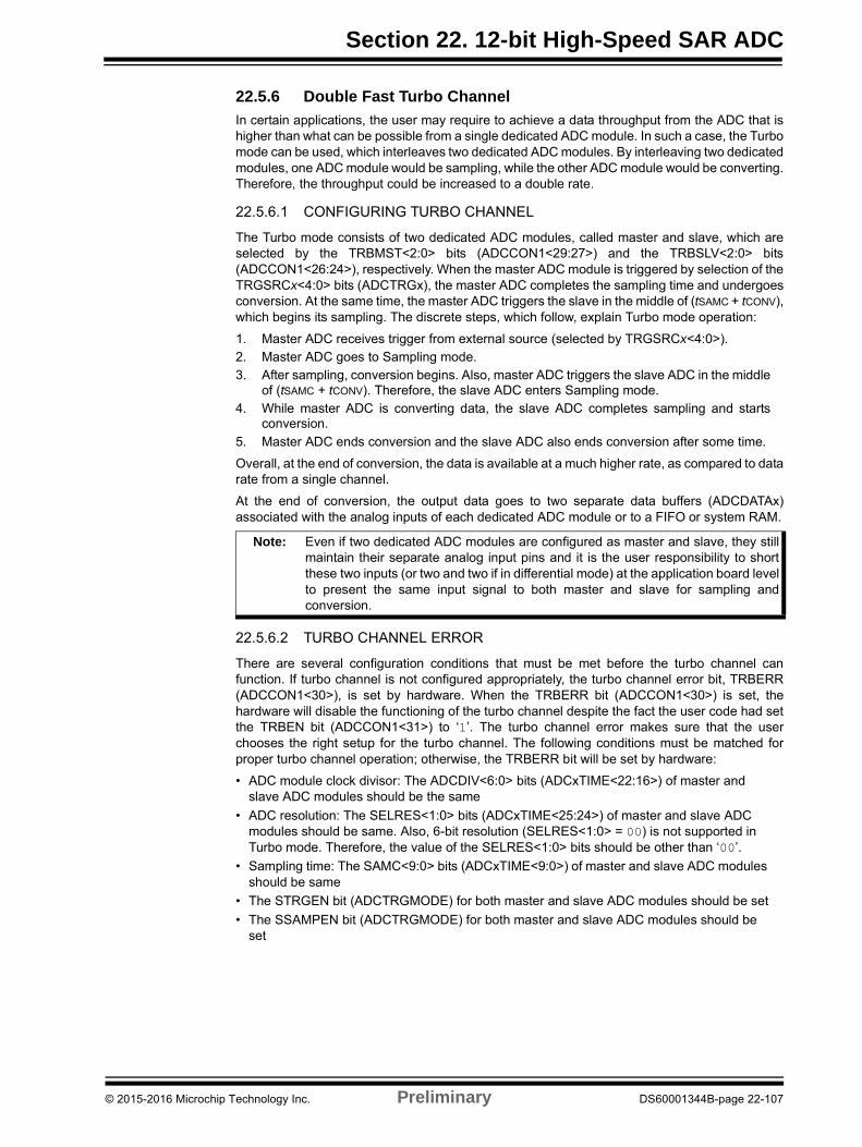
Section 22. 12-bit High-Speed SAR ADC
22.5.6 Double Fast Turbo Channel
In certain applications, the user may require to achieve a data throughput from the ADC that ishigher than what can be possible from a single dedicated ADC module. In such a case, the Turbomode can be used, which interleaves two dedicated ADC modules. By interleaving two dedicatedmodules, one ADC module would be sampling, while the other ADC module would be converting.Therefore, the throughput could be increased to a double rate.
22.5.6.1 CONFIGURING TURBO CHANNEL
The Turbo mode consists of two dedicated ADC modules, called master and slave, which areselected by the TRBMST<2:0> bits (ADCCON1<29:27>) and the TRBSLV<2:0> bits(ADCCON1<26:24>), respectively. When the master ADC module is triggered by selection of theTRGSRCx<4:0> bits (ADCTRGx), the master ADC completes the sampling time and undergoesconversion. At the same time, the master ADC triggers the slave in the middle of (tSAMC + tCONV),which begins its sampling. The discrete steps, which follow, explain Turbo mode operation:
1. Master ADC receives trigger from external source (selected by TRGSRCx<4:0>).2. Master ADC goes to Sampling mode.3. After sampling, conversion begins. Also, master ADC triggers the slave ADC in the middle
of (tSAMC + tCONV). Therefore, the slave ADC enters Sampling mode.4. While master ADC is converting data, the slave ADC completes sampling and starts
conversion.
5. Master ADC ends conversion and the slave ADC also ends conversion after some time.
Overall, at the end of conversion, the data is available at a much higher rate, as compared to datarate from a single channel.
At the end of conversion, the output data goes to two separate data buffers (ADCDATAx)associated with the analog inputs of each dedicated ADC module or to a FIFO or system RAM.
22.5.6.2 TURBO CHANNEL ERROR
There are several configuration conditions that must be met before the turbo channel canfunction. If turbo channel is not configured appropriately, the turbo channel error bit, TRBERR(ADCCON1<30>), is set by hardware. When the TRBERR bit (ADCCON1<30>) is set, thehardware will disable the functioning of the turbo channel despite the fact the user code had setthe TRBEN bit (ADCCON1<31>) to ‘1’. The turbo channel error makes sure that the userchooses the right setup for the turbo channel. The following conditions must be matched forproper turbo channel operation; otherwise, the TRBERR bit will be set by hardware:
• ADC module clock divisor: The ADCDIV<6:0> bits (ADCxTIME<22:16>) of master and slave ADC modules should be the same
• ADC resolution: The SELRES<1:0> bits (ADCxTIME<25:24>) of master and slave ADC modules should be same. Also, 6-bit resolution (SELRES<1:0> = 00) is not supported in Turbo mode. Therefore, the value of the SELRES<1:0> bits should be other than ‘00’.
• Sampling time: The SAMC<9:0> bits (ADCxTIME<9:0>) of master and slave ADC modules should be same
• The STRGEN bit (ADCTRGMODE) for both master and slave ADC modules should be set
• The SSAMPEN bit (ADCTRGMODE) for both master and slave ADC modules should be set
Note: Even if two dedicated ADC modules are configured as master and slave, they stillmaintain their separate analog input pins and it is the user responsibility to shortthese two inputs (or two and two if in differential mode) at the application board levelto present the same input signal to both master and slave for sampling andconversion.
© 2015-2016 Microchip Technology Inc. Preliminary DS60001344B-page 22-107
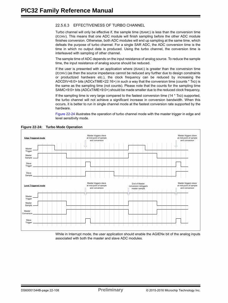
PIC32 Family Reference Manual
22.5.6.3 EFFECTIVENESS OF TURBO CHANNEL
Turbo channel will only be effective if, the sample time (tSAMC) is less than the conversion time(tCONV). This means that one ADC module will finish sampling before the other ADC modulefinishes conversion. Otherwise, both ADC modules will end up sampling at the same time, whichdefeats the purpose of turbo channel. For a single SAR ADC, the ADC conversion time is thetime in which no output data is produced. Using the turbo channel, the conversion time isinterleaved with sampling of other channel.
The sample time of ADC depends on the input resistance of analog source. To reduce the sampletime, the input resistance of analog source should be reduced.
If the user is presented with an application where (tSAMC) is greater than the conversion time(tCONV) (as then the source impedance cannot be reduced any further due to design constraintsor productized hardware etc.), the clock frequency can be reduced by increasing theADCDIV<6:0> bits (ADCxTIME<22:16>) in such a way that the conversion time (counts * TAD) isthe same as the sampling time (not counts). Please note that the counts for the sampling timeSAMC<9:0> bits (ADCxTIME<9:0>) should be made smaller due to the reduced clock frequency.
If the sampling time is very large compared to the fastest conversion time (14 * TAD) supported,the turbo channel will not achieve a significant increase in conversion bandwidth. When thisoccurs, it is better to run in single channel mode at the fastest conversion rate supported by thehardware.
Figure 22-24 illustrates the operation of turbo channel mode with the master trigger in edge andlevel sensitivity mode.
Figure 22-24: Turbo Mode Operation
While in Interrupt mode, the user application should enable the AGIENx bit of the analog inputsassociated with both the master and slave ADC modules.
Edge Triggered mode
Master Trigger
Master Sample
Slave Trigger
Master triggers slave at mid-point of sample
and conversion
Master triggers slave at mid-point of sample
and conversion
SlaveSample
Level Triggered mode
Master Trigger
Master Sample
MasterConversion
Master triggers slave at mid-point of sample
and conversion
Master triggers slave at mid-point of sample
and conversion
Slave Trigger
End of Master conversion retriggers
master sample
DS60001344B-page 22-108 Preliminary © 2015-2016 Microchip Technology Inc.
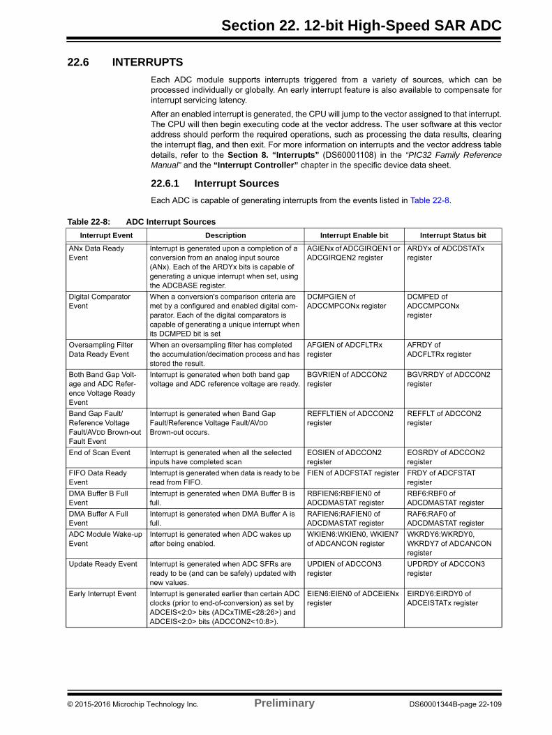
Section 22. 12-bit High-Speed SAR ADC
22.6 INTERRUPTS
Each ADC module supports interrupts triggered from a variety of sources, which can beprocessed individually or globally. An early interrupt feature is also available to compensate forinterrupt servicing latency.
After an enabled interrupt is generated, the CPU will jump to the vector assigned to that interrupt.The CPU will then begin executing code at the vector address. The user software at this vectoraddress should perform the required operations, such as processing the data results, clearingthe interrupt flag, and then exit. For more information on interrupts and the vector address tabledetails, refer to the Section 8. “Interrupts” (DS60001108) in the “PIC32 Family ReferenceManual” and the “Interrupt Controller” chapter in the specific device data sheet.
22.6.1 Interrupt Sources
Each ADC is capable of generating interrupts from the events listed in Table 22-8.
Table 22-8: ADC Interrupt Sources
Interrupt Event Description Interrupt Enable bit Interrupt Status bit
ANx Data Ready Event
Interrupt is generated upon a completion of a conversion from an analog input source (ANx). Each of the ARDYx bits is capable of generating a unique interrupt when set, using the ADCBASE register.
AGIENx of ADCGIRQEN1 or ADCGIRQEN2 register
ARDYx of ADCDSTATx register
Digital Comparator Event
When a conversion's comparison criteria are met by a configured and enabled digital com-parator. Each of the digital comparators is capable of generating a unique interrupt when its DCMPED bit is set
DCMPGIEN of ADCCMPCONx register
DCMPED of ADCCMPCONxregister
Oversampling Filter Data Ready Event
When an oversampling filter has completed the accumulation/decimation process and has stored the result.
AFGIEN of ADCFLTRx register
AFRDY ofADCFLTRx register
Both Band Gap Volt-age and ADC Refer-ence Voltage Ready Event
Interrupt is generated when both band gap voltage and ADC reference voltage are ready.
BGVRIEN of ADCCON2 register
BGVRRDY of ADCCON2 register
Band Gap Fault/Reference Voltage Fault/AVDD Brown-out Fault Event
Interrupt is generated when Band Gap Fault/Reference Voltage Fault/AVDD Brown-out occurs.
REFFLTIEN of ADCCON2 register
REFFLT of ADCCON2 register
End of Scan Event Interrupt is generated when all the selected inputs have completed scan
EOSIEN of ADCCON2 register
EOSRDY of ADCCON2 register
FIFO Data Ready Event
Interrupt is generated when data is ready to be read from FIFO.
FIEN of ADCFSTAT register FRDY of ADCFSTAT register
DMA Buffer B Full Event
Interrupt is generated when DMA Buffer B is full.
RBFIEN6:RBFIEN0 of ADCDMASTAT register
RBF6:RBF0 of ADCDMASTAT register
DMA Buffer A Full Event
Interrupt is generated when DMA Buffer A is full.
RAFIEN6:RAFIEN0 of ADCDMASTAT register
RAF6:RAF0 of ADCDMASTAT register
ADC Module Wake-up Event
Interrupt is generated when ADC wakes up after being enabled.
WKIEN6:WKIEN0, WKIEN7 of ADCANCON register
WKRDY6:WKRDY0, WKRDY7 of ADCANCON register
Update Ready Event Interrupt is generated when ADC SFRs are ready to be (and can be safely) updated with new values.
UPDIEN of ADCCON3 register
UPDRDY of ADCCON3 register
Early Interrupt Event Interrupt is generated earlier than certain ADC clocks (prior to end-of-conversion) as set by ADCEIS<2:0> bits (ADCxTIME<28:26>) and ADCEIS<2:0> bits (ADCCON2<10:8>).
EIEN6:EIEN0 of ADCEIENx register
EIRDY6:EIRDY0 of ADCEISTATx register
© 2015-2016 Microchip Technology Inc. Preliminary DS60001344B-page 22-109
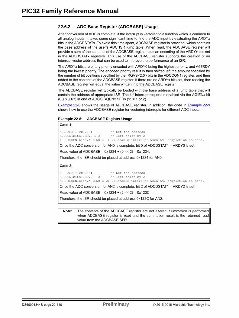
PIC32 Family Reference Manual
22.6.2 ADC Base Register (ADCBASE) Usage
After conversion of ADC is complete, if the interrupt is vectored to a function which is common toall analog inputs, it takes some significant time to find the ADC input by evaluating the ARDYxbits in the ADCDSTATx. To avoid this time spent, ADCBASE register is provided, which containsthe base address of the user’s ADC ISR jump table. When read, the ADCBASE register willprovide a sum of the contents of the ADCBASE register plus an encoding of the ARDYx bits setin the ADCDSTATx registers. This use of the ADCBASE register supports the creation of aninterrupt vector address that can be used to improve the performance of an ISR.
The ARDYx bits are binary priority encoded with ARDY0 being the highest priority, and A63RDYbeing the lowest priority. The encoded priority result is then shifted left the amount specified bythe number of bit positions specified by the IRQVS<2:0> bits in the ADCCON1 register, and thenadded to the contents of the ADCBASE register. If there are no ARDYx bits set, then reading theADCBASE register will equal the value written into the ADCBASE register.
The ADCBASE register will typically be loaded with the base address of a jump table that willcontain the address of appropriate ISR. The kth interrupt request is enabled via the AGIENx bit(0 x 63) in one of ADCGIRQENx SFRs (‘x’ = 1 or 2).
Example 22-8 shows the usage of ADCBASE register. In addition, the code in Example 22-9shows how to use the ADCBASE register for vectoring interrupts for different ADC inputs.
Example 22-8: ADCBASE Register Usage
Note: The contents of the ADCBASE register are not altered. Summation is performedwhen ADCBASE register is read and the summation result is the returned readvalue from the ADCBASE SFR.
Case 1:
ADCBASE = 0x1234; // Set the addressADCCON1bits.IRQVS = 2; // left shift by 2ADCGIRQEN1bits.AGIEN0 = 1; // enable interrupt when AN0 completion is done.
Once the ADC conversion for AN0 is complete, bit 0 of ADCDSTAT1 = ARDY0 is set.
Read value of ADCBASE = 0x1234 + (0 << 2) = 0x1234.
Therefore, the ISR should be placed at address 0x1234 for AN0.
Case 2:
ADCBASE = 0x1234; // Set the addressADCCON1bits.IRQVS = 2; // left shift by 2ADCGIRQEN1bits.AGIEN0 = 2; // enable interrupt when AN2 completion is done.
Once the ADC conversion for AN2 is complete, bit 2 of ADCDSTAT1 = ARDY2 is set.
Read value of ADCBASE = 0x1234 + (2 << 2) = 0x123C.
Therefore, the ISR should be placed at address 0x123C for AN2.
DS60001344B-page 22-110 Preliminary © 2015-2016 Microchip Technology Inc.
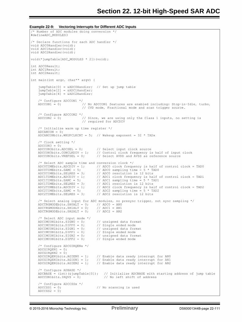
Section 22. 12-bit High-Speed SAR ADC
Example 22-9: Vectoring Interrupts for Different ADC Inputs/* Number of ADC modules doing conversion */#defineADC_MODULES3
/* Declare functions for each ADC handler */void ADC0Handler(void);void ADC1Handler(void);void ADC2Handler(void);
void(*jumpTable[ADC_MODULES * 2])(void);
int ADC0Result;int ADC1Result;int ADC2Result;
int main(int argc, char** argv) {
jumpTable[0] = &ADC0Handler; // Set up jump tablejumpTable[2] = &ADC1Handler;jumpTable[4] = &ADC2Handler;
/* Configure ADCCON1 */ADCCON1 = 0; // No ADCCON1 features are enabled including: Stop-in-Idle, turbo,
// CVD mode, Fractional mode and scan trigger source.
/* Configure ADCCON2 */ADCCON2 = 0; // Since, we are using only the Class 1 inputs, no setting is
// required for ADCDIV
/* Initialize warm up time register */ADCANCON = 0;ADCANCONbits.WKUPCLKCNT = 5; // Wakeup exponent = 32 * TADx
/* Clock setting */ADCCON3 = 0;ADCCON3bits.ADCSEL = 0; // Select input clock sourceADCCON3bits.CONCLKDIV = 1; // Control clock frequency is half of input clockADCCON3bits.VREFSEL = 0; // Select AVDD and AVSS as reference source
/* Select ADC sample time and conversion clock */ADC0TIMEbits.ADCDIV = 1; // ADC0 clock frequency is half of control clock = TAD0ADC0TIMEbits.SAMC = 5; // ADC0 sampling time = 5 * TAD0ADC0TIMEbits.SELRES = 3; // ADC0 resolution is 12 bitsADC1TIMEbits.ADCDIV = 1; // ADC1 clock frequency is half of control clock = TAD1ADC1TIMEbits.SAMC = 5; // ADC1 sampling time = 5 * TAD1ADC1TIMEbits.SELRES = 3; // ADC1 resolution is 12 bitsADC2TIMEbits.ADCDIV = 1; // ADC2 clock frequency is half of control clock = TAD2ADC2TIMEbits.SAMC = 5; // ADC2 sampling time = 5 * TAD2ADC2TIMEbits.SELRES = 3; // ADC2 resolution is 12 bits
/* Select analog input for ADC modules, no presync trigger, not sync sampling */ADCTRGMODEbits.SH0ALT = 0; // ADC0 = AN0ADCTRGMODEbits.SH1ALT = 0; // ADC1 = AN1ADCTRGMODEbits.SH2ALT = 0; // ADC2 = AN2
/* Select ADC input mode */ADCIMCON1bits.SIGN0 = 0; // unsigned data formatADCIMCON1bits.DIFF0 = 0; // Single ended modeADCIMCON1bits.SIGN1 = 0; // unsigned data formatADCIMCON1bits.DIFF1 = 0; // Single ended modeADCIMCON1bits.SIGN2 = 0; // unsigned data formatADCIMCON1bits.DIFF2 = 0; // Single ended mode
/* Configure ADCGIRQENx */ADCGIRQEN1 = 0; ADCGIRQEN2 = 0;ADCGIRQEN1bits.AGIEN0 = 1; // Enable data ready interrupt for AN0ADCGIRQEN1bits.AGIEN1 = 1; // Enable data ready interrupt for AN1ADCGIRQEN1bits.AGIEN2 = 1; // Enable data ready interrupt for AN2
/* Configure ADBASE */ADCBASE = (int)(&jumpTable[0]); // Initialize ADCBASE with starting address of jump tableADCCON1bits.IRQVS = 0; // No left shift of address
/* Configure ADCCSSx */ADCCSS1 = 0; // No scanning is usedADCCSS2 = 0;
© 2015-2016 Microchip Technology Inc. Preliminary DS60001344B-page 22-111
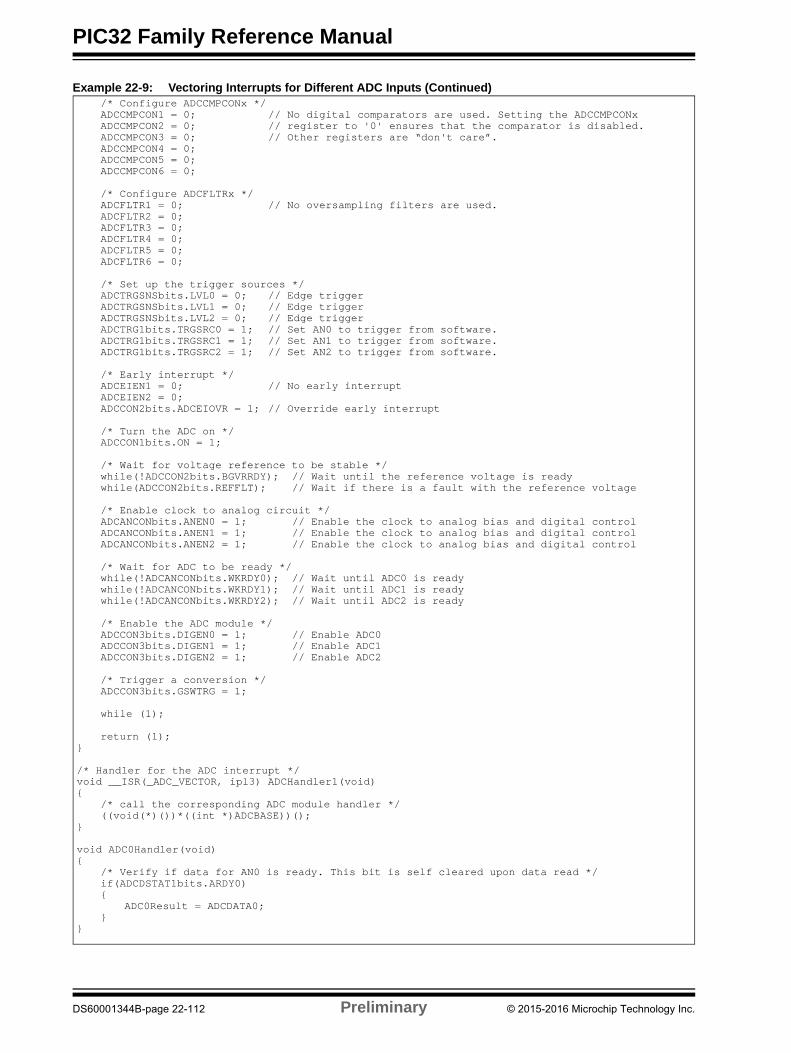
PIC32 Family Reference Manual
Example 22-9: Vectoring Interrupts for Different ADC Inputs (Continued)/* Configure ADCCMPCONx */ADCCMPCON1 = 0; // No digital comparators are used. Setting the ADCCMPCONxADCCMPCON2 = 0; // register to '0' ensures that the comparator is disabled.ADCCMPCON3 = 0; // Other registers are “don't care”.ADCCMPCON4 = 0;ADCCMPCON5 = 0;ADCCMPCON6 = 0;
/* Configure ADCFLTRx */ADCFLTR1 = 0; // No oversampling filters are used.ADCFLTR2 = 0;ADCFLTR3 = 0;ADCFLTR4 = 0;ADCFLTR5 = 0;ADCFLTR6 = 0;
/* Set up the trigger sources */ADCTRGSNSbits.LVL0 = 0; // Edge triggerADCTRGSNSbits.LVL1 = 0; // Edge triggerADCTRGSNSbits.LVL2 = 0; // Edge triggerADCTRG1bits.TRGSRC0 = 1; // Set AN0 to trigger from software.ADCTRG1bits.TRGSRC1 = 1; // Set AN1 to trigger from software.ADCTRG1bits.TRGSRC2 = 1; // Set AN2 to trigger from software.
/* Early interrupt */ADCEIEN1 = 0; // No early interruptADCEIEN2 = 0;ADCCON2bits.ADCEIOVR = 1; // Override early interrupt
/* Turn the ADC on */ADCCON1bits.ON = 1;
/* Wait for voltage reference to be stable */while(!ADCCON2bits.BGVRRDY); // Wait until the reference voltage is readywhile(ADCCON2bits.REFFLT); // Wait if there is a fault with the reference voltage
/* Enable clock to analog circuit */ADCANCONbits.ANEN0 = 1; // Enable the clock to analog bias and digital controlADCANCONbits.ANEN1 = 1; // Enable the clock to analog bias and digital controlADCANCONbits.ANEN2 = 1; // Enable the clock to analog bias and digital control
/* Wait for ADC to be ready */while(!ADCANCONbits.WKRDY0); // Wait until ADC0 is readywhile(!ADCANCONbits.WKRDY1); // Wait until ADC1 is readywhile(!ADCANCONbits.WKRDY2); // Wait until ADC2 is ready
/* Enable the ADC module */ADCCON3bits.DIGEN0 = 1; // Enable ADC0ADCCON3bits.DIGEN1 = 1; // Enable ADC1ADCCON3bits.DIGEN2 = 1; // Enable ADC2
/* Trigger a conversion */ADCCON3bits.GSWTRG = 1;
while (1);
return (1);}
/* Handler for the ADC interrupt */void __ISR(_ADC_VECTOR, ipl3) ADCHandler1(void){
/* call the corresponding ADC module handler */((void(*)())*((int *)ADCBASE))();
}
void ADC0Handler(void){
/* Verify if data for AN0 is ready. This bit is self cleared upon data read */if(ADCDSTAT1bits.ARDY0){
ADC0Result = ADCDATA0;}
}
DS60001344B-page 22-112 Preliminary © 2015-2016 Microchip Technology Inc.
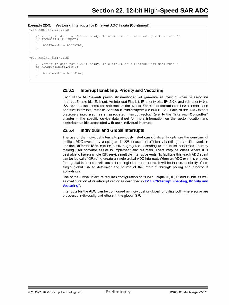
Section 22. 12-bit High-Speed SAR ADC
Example 22-9: Vectoring Interrupts for Different ADC Inputs (Continued)
22.6.3 Interrupt Enabling, Priority and Vectoring
Each of the ADC events previously mentioned will generate an interrupt when its associateInterrupt Enable bit, IE, is set. An Interrupt Flag bit, IF, priority bits, IP<2:0>, and sub-priority bitsIS<1:0> are also associated with each of the events. For more information on how to enable andprioritize interrupts, refer to Section 8. “Interrupts” (DS60001108). Each of the ADC eventspreviously listed also has an associated interrupt vector. Refer to the “Interrupt Controller”chapter in the specific device data sheet for more information on the vector location andcontrol/status bits associated with each individual interrupt.
22.6.4 Individual and Global Interrupts
The use of the individual interrupts previously listed can significantly optimize the servicing ofmultiple ADC events, by keeping each ISR focused on efficiently handling a specific event. Inaddition, different ISRs can be easily segregated according to the tasks performed, therebymaking user software easier to implement and maintain. There may be cases where it isdesirable to have a single ISR service multiple interrupt events. To facilitate this, each ADC eventcan be logically “ORed” to create a single global ADC interrupt. When an ADC event is enabledfor a global interrupt, it will vector to a single interrupt routine. It will be the responsibility of thissingle global ISR to determine the source of the interrupt through polling and process itaccordingly.
Use of the Global Interrupt requires configuration of its own unique IE, IF, IP and IS bits as wellas configuration of its interrupt vector as described in 22.6.3 “Interrupt Enabling, Priority andVectoring”.
Interrupts for the ADC can be configured as individual or global, or utilize both where some areprocessed individually and others in the global ISR.
void ADC1Handler(void){
/* Verify if data for AN1 is ready. This bit is self cleared upon data read */if(ADCDSTAT1bits.ARDY1){
ADC1Result = ADCDATA1;}
}
void ADC2Handler(void){
/* Verify if data for AN2 is ready. This bit is self cleared upon data read */if(ADCDSTAT2bits.ARDY2){
ADC2Result = ADCDATA2;}
}
© 2015-2016 Microchip Technology Inc. Preliminary DS60001344B-page 22-113
PIC32 Family Reference Manual
22.6.5 Early Interrupts
The early interrupt feature lets ADC module generate interrupt before the conversion is complete.Even though the input is still in the conversion process, the processor application software canuse the “head-start” to begin execution of the entry into the ISR. The early interrupt can improvethe throughput of a system by overlapping the completion of the ADC conversion with theprocessor overhead associated with an interrupt. The ADCEIS<2:0> bits (ADCxTIME<28:26>)and ADCEIS<2:0> bits (ADCCON2<10:8>) sets the number of ADC clock prior to which, theinterrupt should occur (for dedicated and shared inputs respectively). Suitably configuring thesebits can reduce the latency from the moment the analog signal was sampled until the point in timewhen the user application software can use the data.
Once the set number of ADC clocks reached prior to end-of-conversion (i.e., prior to data actuallybeing available in the ADCDATAx register), the corresponding early interrupt ready bit, EIRDYx,in the ADCEISTAT1 or ADCEISTAT2 register is set. If the respective interrupt enable bit, EIENx,in the ADCEIEN1 or ADCEIEN2 register is set, the interrupt will be generated.
The early interrupt feature can be overridden by setting the Early Interrupt Override bit,ADCEIOVR (ADCCON2<12>). Once this bit is set, setting the bits in the ADCEIEN1 orADCEIEN2 register has no effect on interrupt generation. The interrupt generation is thencontrolled by the setting of ADCGIRQEN1 and ADCGIRQEN2 registers.
Note: The ADCEIS<2:0> bits setting does not apply to the Oversampling Filter DataReady signal, AFRDY.
DS60001344B-page 22-114 Preliminary © 2015-2016 Microchip Technology Inc.
Section 22. 12-bit High-Speed SAR ADC
22.7 OPERATION DURING POWER-SAVING MODESThe power-saving modes, Sleep and Idle, are useful for reducing the conversion noise byminimizing the digital activity of the CPU, buses and other peripherals.
22.7.1 Sleep Mode
When device enters Sleep mode, the system clock (SYCCLK) is halted. If an ADC moduleselects SYSCLK as its clock source or selects REFCLK3 as its clock source (REFCLK3 isgenerated from SYSCLK), the ADC will enter the Sleep mode.
When the SYSCLK is the source, (directly or indirectly) and Sleep mode occurs during aconversion, the conversion is aborted. The converter will not resume a partially completedconversion on exiting from Sleep mode. The ADC register contents are not affected by the deviceentering or leaving Sleep mode. The ADC module can operate during Sleep mode if the ADCclock source is derived from a source other than SYSCLK that is active during Sleep mode. TheFRC clock source is a logical choice for operation during Sleep; however, the REFCLK3 clocksource can also be used, provided it has an input clock that is operational during Sleep mode.
ADC operation during Sleep mode reduces the digital switching noise from the conversion. Whenthe conversion is completed, the ARDYx status bit for that analog input will be set and the resultwill be loaded into the corresponding ADC Result register (ADCDATAx).
If any of the ADC interrupts is enabled, the device will wake-up from Sleep mode when the ADCinterrupt occurs. The program execution will resume at the ADC ISR, if the ADC interrupt isgreater than the current CPU priority. Otherwise, execution will continue from the instruction afterthe WAIT instruction that placed the device in Sleep mode.
To minimize the effects of digital noise on the ADC module operation, the user must select aconversion trigger source that ensures that the analog-to-digital conversion will take place inSleep mode. For example, the external interrupt pin (INT0) conversion trigger option(TRGSRC<4:0> = 00100) can be used for performing sampling and conversion while the deviceis in Sleep mode.
22.7.2 ADC Operation During Idle Mode
For the ADC, the Stop in Idle Mode bit, SIDL (ADCCON1<13>), specifies whether the ADCmodule will stop on Idle or continue on Idle. If SIDL = 0, the ADC module will continue normaloperation when the device enters Idle mode. If any of the ADC interrupts are enabled, the devicewill wake-up from Idle mode when the ADC interrupt occurs. The program execution will resumeat the ADC ISR if the ADC interrupt is greater than the current CPU priority. Otherwise, executionwill continue from the instruction after the WAIT instruction that placed the device in Idle mode.
If SIDL = 1, the ADC module will stop in Idle mode. If the device enters Idle mode during aconversion, the conversion is aborted. The converter will not resume a partially completedconversion on exiting from Idle mode.
Note: For the ADC module to operate in Sleep mode, the ADC clock source must be setto Internal FRC (ADCSEL<1:0> bits (ADCCON2<31:30>) = 01). Alternately, theREFCLK3 source can be used; however, the clock source used for REFCLK3 mustoperate during Sleep. Any changes to the ADC clock configuration require that theADC be disabled.
© 2015-2016 Microchip Technology Inc. Preliminary DS60001344B-page 22-115

PIC32 Family Reference Manual
22.7.3 ADC Low-power Mode
The ADC module can be placed in a low-power state by disabling the digital circuit for individualADC modules, which are not running. This is possible by clearing the DIGENx bits and theDIGEN7 bit in the ADCCON3 register (see Register 22-3).
An even lower power state is possible by disabling the analog and bias circuit for individual ADCmodules, which are not running. This is possible by clearing the ANENx bits and the ANEN7 bitin the ADCANCON register (see Register 22-41). Disabling the digital circuit to achieveLow-power mode provides a significantly faster module restart compared to disabling andre-enabling the analog and bias circuit of the ADC module. This is because disabling andre-enabling the analog and bias circuit using the ANENx bits and the ANEN7 bit requires awake-up time (typical minimum wake-up time of 20 µs) for the ADC module, before it can beused. Refer to the “Electrical Characteristics” chapter in the specific device data sheet formore information on the stabilization time.
Once the analog and bias circuit for an ADC module is enabled, the wake-up should be polled(or through an interrupt) using the wake-up ready bits, WKRDY6:WKRDY0 and WKRDY7, whichshould be equal to ‘1’.
DS60001344B-page 22-116 Preliminary © 2015-2016 Microchip Technology Inc.
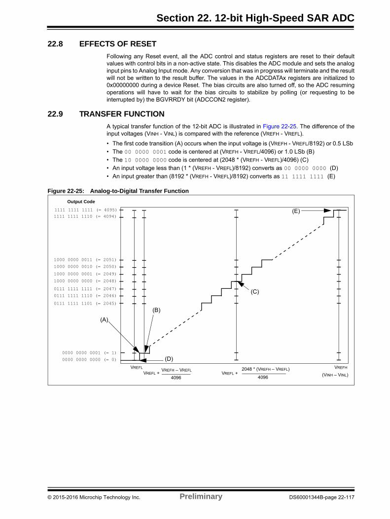
Section 22. 12-bit High-Speed SAR ADC
22.8 EFFECTS OF RESET
Following any Reset event, all the ADC control and status registers are reset to their defaultvalues with control bits in a non-active state. This disables the ADC module and sets the analoginput pins to Analog Input mode. Any conversion that was in progress will terminate and the resultwill not be written to the result buffer. The values in the ADCDATAx registers are initialized to0x00000000 during a device Reset. The bias circuits are also turned off, so the ADC resumingoperations will have to wait for the bias circuits to stabilize by polling (or requesting to beinterrupted by) the BGVRRDY bit (ADCCON2 register).
22.9 TRANSFER FUNCTION
A typical transfer function of the 12-bit ADC is illustrated in Figure 22-25. The difference of theinput voltages (VINH - VINL) is compared with the reference (VREFH - VREFL).
• The first code transition (A) occurs when the input voltage is (VREFH - VREFL/8192) or 0.5 LSb • The 00 0000 0001 code is centered at (VREFH - VREFL/4096) or 1.0 LSb (B)• The 10 0000 0000 code is centered at (2048 * (VREFH - VREFL)/4096) (C)• An input voltage less than (1 * (VREFH - VREFL)/8192) converts as 00 0000 0000 (D)
• An input greater than (8192 * (VREFH - VREFL)/8192) converts as 11 1111 1111 (E)
Figure 22-25: Analog-to-Digital Transfer Function
1000 0000 0001 (= 2049)
1000 0000 0010 (= 2050)
1000 0000 0011 (= 2051)
0111 1111 1101 (= 2045)
0111 1111 1110 (= 2046)
0111 1111 1111 (= 2047)
1111 1111 1110 (= 4094)1111 1111 1111 (= 4095)
0000 0000 0000 (= 0)
0000 0000 0001 (= 1)
Output Code
1000 0000 0000 (= 2048)
(VINH – VINL)
VREFLVREFH – VREFL
4096
2048 * (VREFH – VREFL)
4096
VREFH
VREFL + VREFL +
(A)
(B)
(C)
(D)
(E)
© 2015-2016 Microchip Technology Inc. Preliminary DS60001344B-page 22-117

PIC32 Family Reference Manual
22.10 ADC SAMPLING REQUIREMENTS
The analog input model of the 12-bit ADC is illustrated in Figure 22-26. The total acquisition timefor the analog-to-digital conversion is a function of the internal circuit settling time and the holdingcapacitor charge time.
For the ADC module to meet its specified accuracy, the charge holding capacitor (CHOLD) mustbe allowed to fully charge to the voltage level on the analog input pin. The analog output sourceimpedance (RS), the interconnect impedance (RIC), and the internal sampling switch (RSS)impedance combine to directly affect the time required to charge the CHOLD. The combinedimpedance of the analog sources must therefore be small enough to fully charge (to withinone-fourth LSB of the desired voltage) the holding capacitor within the selected sample time. Theinternal holding capacitor will be in the discharged state prior to each sample operation.
At least 1 TAD time period should be allowed between conversions for the acquisition time. Referto the “Electrical Characteristics” chapter in the specific device data sheet for moreinformation.
Figure 22-26: 12-bit ADC Analog Input Model
22.11 CONNECTION CONSIDERATIONS
Because the analog inputs employ Electrostatic Discharge (ESD) protection, they have diodesto VDD and VSS; therefore, the analog input must be between VDD and VSS. The presence ofdiodes is the reason why the analog pins cannot be 5V tolerant. If the input voltage exceeds thisrange by greater than 0.3V (either direction), one of the diodes becomes forward biased and itmay damage the device if the input current specification exceeds.
An external RC filter is sometimes added for anti-aliasing of the input signal. The R (resistive)component should be selected to ensure that the acquisition time is met. Any externalcomponents connected (through high-impedance) to an analog input pin (capacitor, Zener diode,and so on) should have very little leakage current at the pin.
CPINVA
Rs ANxVT = 0.6V
VT = 0.6VILEAKAGE
RIC = 200 SamplingSwitch
RSS
CHOLD= DAC capacitance
VSS
VDD
= 5 pF± 500 nA
Note: The CPIN value depends on the device package and is not tested. The effect of the CPIN isnegligible if Rs 5 k.
RSS = 44
Legend:
CPIN = Input capacitance VT = Threshold voltage
RSS = Sampling switch resistance RIC = Interconnect resistance
RS = Source resistance CHOLD = Sample/hold capacitance
ILEAKAGE = Leakage current at the pin due to various junctions
DS60001344B-page 22-118 Preliminary © 2015-2016 Microchip Technology Inc.
Section 22. 12-bit High-Speed SAR ADC
22.12 RELATED APPLICATION NOTES
This section lists application notes that are related to this section of the manual. Theseapplication notes may not be written specifically for the PIC32 device family, but the concepts arepertinent and could be used with modification and possible limitations. The current applicationnotes related to the 12-bit High-Speed Successive Approximation Register (SAR)Analog-to-Digital Converter (ADC) module are:
Title Application Note #
No related application notes at this time. N/A
Note: Please visit the Microchip web site (www.microchip.com) for additional applicationnotes and code examples for the PIC32 family of devices.
© 2015-2016 Microchip Technology Inc. Preliminary DS60001344B-page 22-119
PIC32 Family Reference Manual
22.13 REVISION HISTORY
Revision A (June 2015)
This is the initial released version of the document.
Revision B (April 2016)
This revision includes the following updates:
• The ADINSEL<5:0> bits in the ADCCON3 register were updated (see Register 22-7)
• The DFMODE bit in the ADCFLTRx register was updated (see Register 22-17)
• Figure 22-18: “ADC Filter Comparisons Example” was added
• The ADC CVD Mode code example was updated (see Example 22-7)
• Minor updates to text and formatting were incorporated throughout the document
DS60001344B-page 22-120 Preliminary © 2015-2016 Microchip Technology Inc.
Note the following details of the code protection feature on Microchip devices:
• Microchip products meet the specification contained in their particular Microchip Data Sheet.
• Microchip believes that its family of products is one of the most secure families of its kind on the market today, when used in the intended manner and under normal conditions.
• There are dishonest and possibly illegal methods used to breach the code protection feature. All of these methods, to our knowledge, require using the Microchip products in a manner outside the operating specifications contained in Microchip’s Data Sheets. Most likely, the person doing so is engaged in theft of intellectual property.
• Microchip is willing to work with the customer who is concerned about the integrity of their code.
• Neither Microchip nor any other semiconductor manufacturer can guarantee the security of their code. Code protection does not mean that we are guaranteeing the product as “unbreakable.”
Code protection is constantly evolving. We at Microchip are committed to continuously improving the code protection features of ourproducts. Attempts to break Microchip’s code protection feature may be a violation of the Digital Millennium Copyright Act. If such actsallow unauthorized access to your software or other copyrighted work, you may have a right to sue for relief under that Act.
Information contained in this publication regarding deviceapplications and the like is provided only for your convenienceand may be superseded by updates. It is your responsibility toensure that your application meets with your specifications.MICROCHIP MAKES NO REPRESENTATIONS ORWARRANTIES OF ANY KIND WHETHER EXPRESS ORIMPLIED, WRITTEN OR ORAL, STATUTORY OROTHERWISE, RELATED TO THE INFORMATION,INCLUDING BUT NOT LIMITED TO ITS CONDITION,QUALITY, PERFORMANCE, MERCHANTABILITY ORFITNESS FOR PURPOSE. Microchip disclaims all liabilityarising from this information and its use. Use of Microchipdevices in life support and/or safety applications is entirely atthe buyer’s risk, and the buyer agrees to defend, indemnify andhold harmless Microchip from any and all damages, claims,suits, or expenses resulting from such use. No licenses areconveyed, implicitly or otherwise, under any Microchipintellectual property rights unless otherwise stated.
2015-2016 Microchip Technology Inc. Prelimin
Microchip received ISO/TS-16949:2009 certification for its worldwide headquarters, design and wafer fabrication facilities in Chandler and Tempe, Arizona; Gresham, Oregon and design centers in California and India. The Company’s quality system processes and procedures are for its PIC® MCUs and dsPIC® DSCs, KEELOQ® code hopping devices, Serial EEPROMs, microperipherals, nonvolatile memory and analog products. In addition, Microchip’s quality system for the design and manufacture of development systems is ISO 9001:2000 certified.
QUALITY MANAGEMENT SYSTEM CERTIFIED BY DNV
== ISO/TS 16949 ==
Trademarks
The Microchip name and logo, the Microchip logo, AnyRate, dsPIC, FlashFlex, flexPWR, Heldo, JukeBlox, KeeLoq, KeeLoq logo, Kleer, LANCheck, LINK MD, MediaLB, MOST, MOST logo, MPLAB, OptoLyzer, PIC, PICSTART, PIC32 logo, RightTouch, SpyNIC, SST, SST Logo, SuperFlash and UNI/O are registered trademarks of Microchip Technology Incorporated in the U.S.A. and other countries.
ClockWorks, The Embedded Control Solutions Company, ETHERSYNCH, Hyper Speed Control, HyperLight Load, IntelliMOS, mTouch, Precision Edge, and QUIET-WIRE are registered trademarks of Microchip Technology Incorporated in the U.S.A.
Analog-for-the-Digital Age, Any Capacitor, AnyIn, AnyOut, BodyCom, chipKIT, chipKIT logo, CodeGuard, dsPICDEM, dsPICDEM.net, Dynamic Average Matching, DAM, ECAN, EtherGREEN, In-Circuit Serial Programming, ICSP, Inter-Chip Connectivity, JitterBlocker, KleerNet, KleerNet logo, MiWi, motorBench, MPASM, MPF, MPLAB Certified logo, MPLIB, MPLINK, MultiTRAK, NetDetach, Omniscient Code Generation, PICDEM, PICDEM.net, PICkit, PICtail, PureSilicon, RightTouch logo, REAL ICE, Ripple Blocker, Serial Quad I/O, SQI, SuperSwitcher, SuperSwitcher II, Total Endurance, TSHARC, USBCheck, VariSense, ViewSpan, WiperLock, Wireless DNA, and ZENA are trademarks of Microchip Technology Incorporated in the U.S.A. and other countries.
SQTP is a service mark of Microchip Technology Incorporated in the U.S.A.
Silicon Storage Technology is a registered trademark of Microchip Technology Inc. in other countries.
GestIC is a registered trademarks of Microchip Technology Germany II GmbH & Co. KG, a subsidiary of Microchip Technology Inc., in other countries.
All other trademarks mentioned herein are property of their respective companies.
© 2015-2016, Microchip Technology Incorporated, Printed in the U.S.A., All Rights Reserved.
ISBN: 978-1-5224-0530-6
ary DS60001344B-page 22-121

DS60001344B-page 22-122 Preliminary 2015-2016 Microchip Technology Inc.
AMERICASCorporate Office2355 West Chandler Blvd.Chandler, AZ 85224-6199Tel: 480-792-7200 Fax: 480-792-7277Technical Support: http://www.microchip.com/supportWeb Address: www.microchip.com
AtlantaDuluth, GA Tel: 678-957-9614 Fax: 678-957-1455
Austin, TXTel: 512-257-3370
BostonWestborough, MA Tel: 774-760-0087 Fax: 774-760-0088
ChicagoItasca, IL Tel: 630-285-0071 Fax: 630-285-0075
ClevelandIndependence, OH Tel: 216-447-0464 Fax: 216-447-0643
DallasAddison, TX Tel: 972-818-7423 Fax: 972-818-2924
DetroitNovi, MI Tel: 248-848-4000
Houston, TX Tel: 281-894-5983
IndianapolisNoblesville, IN Tel: 317-773-8323Fax: 317-773-5453
Los AngelesMission Viejo, CA Tel: 949-462-9523 Fax: 949-462-9608
New York, NY Tel: 631-435-6000
San Jose, CA Tel: 408-735-9110
Canada - TorontoTel: 905-673-0699 Fax: 905-673-6509
ASIA/PACIFICAsia Pacific OfficeSuites 3707-14, 37th FloorTower 6, The GatewayHarbour City, Kowloon
Hong KongTel: 852-2943-5100Fax: 852-2401-3431
Australia - SydneyTel: 61-2-9868-6733Fax: 61-2-9868-6755
China - BeijingTel: 86-10-8569-7000 Fax: 86-10-8528-2104
China - ChengduTel: 86-28-8665-5511Fax: 86-28-8665-7889
China - ChongqingTel: 86-23-8980-9588Fax: 86-23-8980-9500
China - DongguanTel: 86-769-8702-9880
China - HangzhouTel: 86-571-8792-8115 Fax: 86-571-8792-8116
China - Hong Kong SARTel: 852-2943-5100 Fax: 852-2401-3431
China - NanjingTel: 86-25-8473-2460Fax: 86-25-8473-2470
China - QingdaoTel: 86-532-8502-7355Fax: 86-532-8502-7205
China - ShanghaiTel: 86-21-5407-5533 Fax: 86-21-5407-5066
China - ShenyangTel: 86-24-2334-2829Fax: 86-24-2334-2393
China - ShenzhenTel: 86-755-8864-2200 Fax: 86-755-8203-1760
China - WuhanTel: 86-27-5980-5300Fax: 86-27-5980-5118
China - XianTel: 86-29-8833-7252Fax: 86-29-8833-7256
ASIA/PACIFICChina - XiamenTel: 86-592-2388138 Fax: 86-592-2388130
China - ZhuhaiTel: 86-756-3210040 Fax: 86-756-3210049
India - BangaloreTel: 91-80-3090-4444 Fax: 91-80-3090-4123
India - New DelhiTel: 91-11-4160-8631Fax: 91-11-4160-8632
India - PuneTel: 91-20-3019-1500
Japan - OsakaTel: 81-6-6152-7160 Fax: 81-6-6152-9310
Japan - TokyoTel: 81-3-6880- 3770 Fax: 81-3-6880-3771
Korea - DaeguTel: 82-53-744-4301Fax: 82-53-744-4302
Korea - SeoulTel: 82-2-554-7200Fax: 82-2-558-5932 or 82-2-558-5934
Malaysia - Kuala LumpurTel: 60-3-6201-9857Fax: 60-3-6201-9859
Malaysia - PenangTel: 60-4-227-8870Fax: 60-4-227-4068
Philippines - ManilaTel: 63-2-634-9065Fax: 63-2-634-9069
SingaporeTel: 65-6334-8870Fax: 65-6334-8850
Taiwan - Hsin ChuTel: 886-3-5778-366Fax: 886-3-5770-955
Taiwan - KaohsiungTel: 886-7-213-7828
Taiwan - TaipeiTel: 886-2-2508-8600 Fax: 886-2-2508-0102
Thailand - BangkokTel: 66-2-694-1351Fax: 66-2-694-1350
EUROPEAustria - WelsTel: 43-7242-2244-39Fax: 43-7242-2244-393
Denmark - CopenhagenTel: 45-4450-2828 Fax: 45-4485-2829
France - ParisTel: 33-1-69-53-63-20 Fax: 33-1-69-30-90-79
Germany - DusseldorfTel: 49-2129-3766400
Germany - KarlsruheTel: 49-721-625370
Germany - MunichTel: 49-89-627-144-0 Fax: 49-89-627-144-44
Italy - Milan Tel: 39-0331-742611 Fax: 39-0331-466781
Italy - VeniceTel: 39-049-7625286
Netherlands - DrunenTel: 31-416-690399 Fax: 31-416-690340
Poland - WarsawTel: 48-22-3325737
Spain - MadridTel: 34-91-708-08-90Fax: 34-91-708-08-91
Sweden - StockholmTel: 46-8-5090-4654
UK - WokinghamTel: 44-118-921-5800Fax: 44-118-921-5820
Worldwide Sales and Service
07/14/15
Related Documents