MOTOROLA MC68328 USER’S MANUAL 11/6/97 1-1 INTRODUCTION 1 PRELIMINARY SECTION 1 INTRODUCTION The MC68328 DragonBall microprocessor is designed to save you time, power, cost, board space, pin count, and programming steps when designing your product. This functionality on a different microprocessor could require 20 separate components, each with 16-64 separate pins. Most of these components require interconnects, which may be duplicates. In fact, each of these connections could not only have a bad solder joint or misrouted trace, but may require another part to qualify, purchase, inventory, and maintain. These components take up valuable space on your PCB and they also consume more power. In addition, the signals between the CPU and a peripheral could be incompatible and may not run from the same clock, which could require time delays or other special design constraints. All this combined makes the DragonBall the microprocessor of choice among many system designers. Its functionality and glue logic are all optimally connected, timed with the same clock, fully tested, and uniformly documented. Also, only the essential signals are brought out to the pins. The DragonBall’s primary package consists of a surface-mount plastic TQFP designed to leave the smallest possible footprint on your board. This manual will discuss the details of how to initialize, configure, and operate the DragonBall microprocessor. However, it assumes you have a basic knowledge of 68K architecture. If you are not familiar with 68K, you should get copies of the M68000 User’s Manual, M68000 Programmer’s Reference Manual, and A Discussion of Interrupts for the MC68000 to use in conjunction with this manual. You can go to the Motorola website at http:/ /www.motorola.com/pso to download these documents or you can contact your local sales office for printed versions. 1.1 FEATURES The following list contains the main features of the DragonBall microprocessor: • MC68EC000 Static Core Processor ❏ 100% Compatibility with MC68000 and MC68EC000 Processors ❏ 32-Bit Internal Address Bus ❏ 24-Bit External Address Bus with Optional 32-Bit Address Bus for a 4G Address Space ❏ 16-Bit On-Chip Data Bus for MC68EC000 Bus Operations ❏ Static Design Allows Processor Clock to Be Stopped to Save Power ❏ 2.7MIPS Performance Using a 16.67MHz Processor Clock • Selectable Bus Sizing Support for Connecting to 8- and 16-Bit Devices

Welcome message from author
This document is posted to help you gain knowledge. Please leave a comment to let me know what you think about it! Share it to your friends and learn new things together.
Transcript
MOTOROLA
MC68328 USER’S MANUAL 11/6/97
1-1
INTR
ODU
CTIO
N
1
PRELIM
INARY
SECTION 1INTRODUCTION
The MC68328 DragonBall microprocessor is designed to save you time, power, cost, board space, pin count, and programming steps when designing your product. This functionality on a different microprocessor could require 20 separate components, each with 16-64 separate pins. Most of these components require interconnects, which may be duplicates. In fact, each of these connections could not only have a bad solder joint or misrouted trace, but may require another part to qualify, purchase, inventory, and maintain. These components take up valuable space on your PCB and they also consume more power. In addition, the signals between the CPU and a peripheral could be incompatible and may not run from the same clock, which could require time delays or other special design constraints.
All this combined makes the DragonBall the microprocessor of choice among many system designers. Its functionality and glue logic are all optimally connected, timed with the same clock, fully tested, and uniformly documented. Also, only the essential signals are brought out to the pins. The DragonBall’s primary package consists of a surface-mount plastic TQFP designed to leave the smallest possible footprint on your board.
This manual will discuss the details of how to initialize, configure, and operate the DragonBall microprocessor. However, it assumes you have a basic knowledge of 68K architecture. If you are not familiar with 68K, you should get copies of the
M68000 User’s Manual
,
M68000 Programmer’s Reference Manual
, and
A Discussion of Interrupts for the MC68000
to use in conjunction with this manual. You can go to the Motorola website at http://www.motorola.com/pso to download these documents or you can contact your local sales office for printed versions.
1.1 FEATURES
The following list contains the main features of the DragonBall microprocessor:
• MC68EC000 Static Core Processor
❏
100% Compatibility with MC68000 and MC68EC000 Processors
❏
32-Bit Internal Address Bus
❏
24-Bit External Address Bus with Optional 32-Bit Address Bus for a 4G Address Space
❏
16-Bit On-Chip Data Bus for MC68EC000 Bus Operations
❏
Static Design Allows Processor Clock to Be Stopped to Save Power
❏
2.7MIPS Performance Using a 16.67MHz Processor Clock
• Selectable Bus Sizing Support for Connecting to 8- and 16-Bit Devices
Introduction
1-2
MC68328 USER’S MANUAL 11/6/97
MOTOROLA
INTRODUCTIO
N
1
PRELIM
INARY
• System Integration Module Supports Glueless System Design
❏
System Configuration and Programmable Address Mapping
❏
Memory Interface for SRAM, EPROM, and Flash Memory
• Sixteen Programmable Peripheral Chip-Selects with Wait-State Generation Logic
❏
PCMCIA 1.0 Support
• Interrupt Controller with 13 Flexible Inputs
❏
Programmable Interrupt Vector Generator
• Maximum of 77 Individually Programmable Parallel Port Signals
• Dual-Channel 16-Bit General-Purpose Counter/Timer
❏
Multimode Operation, Independent Capture and Compare Registers
❏
Automatic Interrupt Generation
❏
60ns Resolution for a 16.67MHz System Clock
❏
Hardware and Software Watchdog Timers
❏
Separate Input and Output Pins for Capture and Compare
• Phase-Locked Loop and Power Management
❏
3.3V Operation
❏
Fully Static HCMOS Technology
❏
Programmable Clock Synthesizer for Full Frequency Control
❏
Doze Mode Capability
❏
Low-Power Mode Control
❏
CPU Can Be Shut Down in Doze Mode
❏
Sleep Mode Can Be Entered By Shutting Down the Phase-Locked Loop (PLL)
• LCD Controller
❏
Software Programmable Screen Size to Drive Single Monochrome/STN Panels
❏
Directly Drives Common LCD Drivers and Modules
❏
Maximum of Four Grayscale Levels
❏
System Memory Can Be Used as Display Memory
• UART
❏
IrDA-Compliant Physical Layer Protocol Support
❏
8-Byte Transmit and Receive FIFOs
• Real-Time Clock
❏
24-Hour Time
❏
Programmable Alarm
• Pulse-Width Modulation Output for Sound Generation
❏
Programmable Frame Rate
❏
16-Bit Programmable
❏
Motor Control Support
• Two Serial Peripheral Interface Ports
Introduction
MOTOROLA
MC68328 USER’S MANUAL 11/6/97
1-3
INTR
ODU
CTIO
N
1
PRELIM
INARY
❏
External POCSAG Decoder (Slave) Support
❏
Digitizer For A/D Input or FLEX Pager (Master) Support
• IEEE 1149.1 Boundary Scan Test Access Port (JTAG)
• Operation From DC To 16.67MHz (Processor Clock)
• Operating Voltage of 3.3V
±
0.3V
• Compact 144-Lead Thin-Quad-Flat-Pack (TQFP) Packaging
MOTOROLA
MC68328 USER’S MANUAL 11/6/97
2-1
SIG
NAL
DESC
RIPT
IONS
2
PRELIM
INARY
SECTION 2SIGNALS
This section contains a description of the MC68328 DragonBall microprocessor signals, as well as the pin assignment of the 144-lead plastic thin-quad flat package (TQFP).
The DragonBall uses a standard M68000 bus for communication between both on-chip and external peripherals with optional address extension to A31. This single continuous bus exists both on the and off the chip. Read accesses made by the core to internal memory-mapped registers of the device are invisible on the external bus. Write accesses made by the core to internal or external memory mapped locations are visible on the external bus.
Signals
2-2
MC68328 USER’S MANUAL 11/6/97
MOTOROLA
SIGNAL DESCRIPTIO
NS
2
PRELIM
INARY
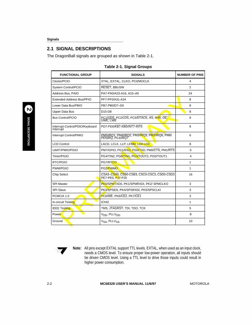
2.1 SIGNAL DESCRIPTIONS
The DragonBall signals are grouped as shown in Table 2-1.
Table 2-1. Signal Groups
FUNCTIONAL GROUP SIGNALS NUMBER OF PINS
Clocks/PCIO XTAL, EXTAL, CLKO, PC0/MOCLK 4
System Control/PCIO RESET, BBUSW 2
Address Bus, PAIO PA7-PA0/A23-A16, A15–A0 24
Extended Address Bus/PFIO PF7-PF0/A31-A24 8
Lower Data Bus/PBIO PB7-PB0/D7–D0 8
Upper Data Bus D15-D8 8
Bus Control/PCIO PC1/UDS, PC2/LDS, PC5/DTACK, AS, R/W, OE, UWE, LWE
8
Interrupt Control/PDIO/Keyboard Interrupt
PD7-PD0/KB7-KB0/INT7-INT0 8
Interrupt Control/PMIO PM5/IRQ1, PM4/IRQ2, PM3/IRQ3, PM2/IRQ6, PM6/PENIRQ, PC4/IRQ7
6
LCD Control LACD, LCLK, LLP, LFRM, LD0-LD3 8
UART/PMIO/PGIO PM7/GPIO, PG1/RXD, PG0/TXD, PM0/CTS, PM1/RTS 5
Timer/PGIO PG4/TIN2, PG6/TIN1, PG3/TOUT2, PG5/TOUT1 4
RTC/PGIO PG7/RTCO 1
PWM/PGIO PG2/PWMO 1
Chip Select CSA3–CSA0, CSB0-CSB3, CSC0-CSC3, CSD0-CSD3PE7-PE0, PJ7-PJ0
16
SPI Master PK0/SPMTXD0, PK1/SPMRXDI, PK2/ SPMCLKO 3
SPI Slave PK3/SPSEN, PK4/SPSRXDI, PK5/SPSCLKI 3
PCMCIA 1.0 PC6/WE, PK6/CE2, PK7/CE1 3
In-circuit Testing ICHIZ 1
IEEE Testing TMS, JTAGRST, TDI, TDO, TCK 5
Power V
DD
, PLLV
DD
8
Ground V
SS
, PLLV
SS
10
Note:
All pins except EXTAL support TTL levels. EXTAL, when used as an input clock,needs a CMOS level. To ensure proper low-power operation, all inputs shouldbe driven CMOS level. Using a TTL level to drive those inputs could result inhigher power consumption.
Signals
2-3
MC68328 USER’S MANUAL 11/6/97
MOTOROLA
SIGNAL DESCRIPTIO
NS
2
PRELIM
INARY
2.1.1 Power Pins
The MC68328 processor has 20 power supply pins. Users should be careful to reduce noise, potential crosstalk, and RF radiation from the output drivers. Inputs may be +5 V or +3.3V when VDD = +3.3V or +5V respectively without damaging the device.
• VDD (7)—7 power pins
• VSS (9)—9 ground pins
• PLLVDD (1)—1 power pin for the PLL
• PLLVSS (1)—1 ground pin for the PLL
2.1.2 4. Clock Pins
EXTAL—EXTERNAL CLOCK/CRYSTAL INPUT
This input provides 3 clock generation options: (1) low frequency crystal, (2) low frequency external clock, and (3) high frequency external clock. While PC0/MOCLK is low, the on-chip phase-locked loop is enabled, creating the high-speed system clock from a low frequency reference. EXTAL may be used (with XTAL) to connect an external crystal to the on-chip oscillator and clock generator. If an external clock instead of a crystal is used, the clock source should be connected to EXTAL, and XTAL left unconnected. The internal PLL generates the system clock at 16.58 MHz from a 32.768 kHz or 38.4 kHz source. When an external clock is used, it must provide a CMOS level at this input frequency.
While PC0/MOCLK is high, the PLL is disabled and the system clock must be connected to the EXTAL pin. If the real-time clock is used, 32.768 kHz or 38.4 kHz must be driven into PG7/RTCO.
XTAL—CRYSTAL OUTPUT
This output connects the on-chip oscillator output to an external crystal. If an external clock is used, XTAL should remain unconnected.
CLKO—CLOCK OUT
This output clock signal is derived from the on-chip clock oscillator and is internally connected to the clock output of the internal PLL. This signal is provided for external reference. The output can be disabled to reduce power consumption.
PC0/MOCLK—Clock Mode Select, Port C I/O
While this pin is high, the MC68328 processor is in the external clock mode and the on-chip PLL is disabled. The system clock must be driven into the EXTAL pin. While this pin is low, it enables the PLL. Either a 32.768 kHz or 38.4 kHz clock can be driven in to the EXTAL pin, or a crystal can be connected between EXTAL and XTAL to create an oscillator. PC0/MOCLK can be programmed as a general-purpose I/O while the internal PLL is enabled.
Signals
2-4
MC68328 USER’S MANUAL 11/6/97
MOTOROLA
SIGNAL DESCRIPTIO
NS
2
PRELIM
INARY
2.1.3 System Control Pins
RESET
This active-low input signal causes the entire MC68328 processor (CPU and peripherals) to enter the reset state (cold reset). Users should drive this signal low for at least 100 msec at initial power-up to ensure that the crystal oscillator starts and stabilizes.
BBUSW—Boot Bus Width-Select
This input defines the data bus width for the boot chip-select, CSA0. BBUSW = 0 means the boot chip-select addresses an 8-bit memory space. BBUSW=1 means the boot memory space is 16-bits wide. Users can create a mixed 8/16 bit memory system by programming the memory space widths in the various chip-select control registers.
2.1.4 Address Bus Pins
These are the address lines driven by the 68EC000 core or by the LCD controller for panel refresh DMA. The chip-select module can decode the entire 4 Gbyte address map. In many applications, only the lower portion of the address lines will be used, reserving any unused address pins for parallel I/O functions.
A15—A0
These address output lines are not multiplexed with any other I/O signals.
PA7-PA0/A16-A23
These address lines are multiplexed with I/O port A. When programmed as I/O ports, they serve as general-purpose I/O ports; otherwise, they are output-only address signals. These signals default to address lines at reset where the address lines are all zeroes. Users should note that there may be contention if any logic “1” levels are driving these pins during or after reset.
PF7-PF0/A31-A24
These bus pins are the extended address for 68EC000 core and are multiplexed with port F. In most systems, these lines are not used as addresses because most memory chips can be mapped into blocks of less than 16 Mbytes. These pins default to the port F I/O function after reset.
2.1.5 Data Bus Pins (D15–D0)
The flexible data bus interface design of the MC68328 processor allows users to program the lower byte of the data bus in an 8-bit-only system as general-purpose I/O signals.
D15–D8
The upper byte of the data bus is not multiplexed with any other signals. In pure 8-bit systems, this is the data bus. In mixed 8-/16-bit systems, 8-bit memory blocks or peripherals should be connected to this bus.
Signals
2-5
MC68328 USER’S MANUAL 11/6/97
MOTOROLA
SIGNAL DESCRIPTIO
NS
2
PRELIM
INARY
PB7–PB0/D7–D0
This bus is the lower data byte or general-purpose I/O. In pure 8-bit systems, this bus can serve as a general-purpose I/O. The WDTH8 bit in the system control register ($FFF000) should be set to one (1) by software before the port can be used. In 16-bit or mixed 8-/16-bit systems, these pins must function as the lower data byte.
2.1.6 Bus Control Pins
AS—ADDRESS STROBE
This active-low output signal indicates that a valid address is present on the address bus. It is not asserted during LCD DMA accesses.
R/W—READ/WRITE
This output signal defines the data bus transfer as a read or write cycle; read = 1; write = 0.
PC1/UDS—UPPER DATA STROBE/PORT C I/O
This pin can be programmed as UDS or as a general-purpose I/O. When used as upper data strobe (UDS) output, this active-low signal is asserted when the internal EC000 core does a 16-bit word access or an even byte access. It is not asserted during LCD DMA accesses.
PC2/LDS—LOWER DATA STROBE/PORT C I/O
This pin can be programmed as LDSor as a general-purpose I/O. When used as lower data strobe (LDS) output, this active-low signal is asserted when the internal EC000 core does a 16-bit word access or an odd byte access. It is not asserted during LCD DMA accesses.
LWE, UWE — LOWER BYTE WRITE-ENABLE AND UPPER BYTE WRITE-ENABLE
On a write cycle to a 16-bit port, these active-low output signals indicate when the upper or lower 8 bits of the data bus contain valid data. In 8-bit mode or when the BSW bit in the chip-select register is 0, use only the upper write-enable (UWE) for write-enable control.
PC4/IRQ7—LEVEL 7 INTERRUPT/PORT C I/O
When programmed as peripherals, this signal is an active-low input which, when asserted, will generate a level 7 interrupt to the CPU. When programmed as I/O, it becomes the PC 4 parallel I/O port.
PC5/DTACK—DATA TRANSFER ACKNOWLEDGE, PC5
This pin can be programmed as parallel I/O PC5 or DTACK. While programmed as DTACK, this input signal indicates that the data transfer has been completed. DTACK is normally generated internally for all chip-selects. For systems that address spaces outside of the chip-select ranges, DTACK must be generated externally. PC5/DTACK must have an external pull-up resistor if programmed for the DTACK function.
OE—OUTPUT-ENABLE
This active-low signal is asserted during a read cycle of the MC68328 processor, which enables the output of either ROM or SRAM. This signal also serves the PCMCIA 1.0 interface to indicate a read cycle.
Signals
2-6
MC68328 USER’S MANUAL 11/6/97
MOTOROLA
SIGNAL DESCRIPTIO
NS
2
PRELIM
INARY
2.1.7 Interrupt Control Pins
PD0-PD7/KB0-KB7/INT0-INT7—KEYBOARD AND GENERAL-PURPOSE INTERRUPT LINES
Users can program these signals as interrupt inputs or parallel I/O ports. For an interrupt port application, INT0-INT7 can be configured to perform keyboard interrupt functions. Keyboard interrupt pins KB0-KB7 are pulled high internally and connected to the rows of the keyboard matrix with the column driven low. When any one key of the row lines is pressed, an interrupt is generated to signal to the CPU to scan the keys. This feature, together with the pen interrupt, contributes a significant portion of the power management activities.
PM6/PENIRQ—PEN INTERRUPT INPUT AND GENERAL-PURPOSE I/O
Users can program this pin as a general-purpose I/O PM6 or pen-interrupt input. When programmed as a pen-interrupt signal, this pin accepts an active low, level-triggered interrupt from the pen input device for a “pen-down” action.
PM5-PM2/IRQ1, IRQ2, IRQ3, IRQ6
These pins can be programmed to either parallel I/O PM2-PM5 or interrupt input. When they function as interrupt inputs, they can be programmed to be edge or level triggered with either high or low polarity. IRQ6 generates a level 6 interrupt. IRQ3, IRQ2, and IRQ1 generate level 3, 2 and 1 interrupts respectively.
2.1.8 Chip Select Pins
CSA0—BOOT CHIP-SELECT
CSA0 is the default chip-select after reset. It is set to 6 wait states and decodes all address ranges except internal register address space. It can be reprogrammed during the boot sequence to another address range and a different number of wait states.
PE7-PE1/CSB3-CSB0, CSA3-CSA1—CHIP-SELECT GROUP A AND B
These pins comprise the remainder of the Group A and Group B chip-selects and are individually programmable. Pins that are not needed as chip-selects can be programmed as general-purpose I/Os. By default after reset, CSB3 is disabled and functions as a general-purpose input.
PJ7-PJ0/CSD3-CSD0/CSC3-CSC0—CHIP-SELECT GROUP C AND D
These pins comprise the Group C and Group D chip-selects and are individually programmable. Pins that are not needed as chip-selects can be programmed as general-purpose I/Os.
2.1.9 PCMCIA 1.0 PINS
PC6/WE—WRITE ENABLE, PC6
This pin can be programmed as either PC6 parallel I/O or a write-enable signal for the PCMCIA 1.0 card interface. The MC68328 processor drives the active-low WE signal to indicate a memory-write transfer to the PCMCIA 1.0 card
.
When programmed as I/O, it serves as PC6.
Signals
2-7
MC68328 USER’S MANUAL 11/6/97
MOTOROLA
SIGNAL DESCRIPTIO
NS
2
PRELIM
INARY
PK7-PK6/CE1-CE2
These pins can be programmed as either parallel I/O port K7-6 or the PCMCIA 1.0 chip-enable signals. When programmed as the PCMCIA chip-enables, CE1 and CE2 are active-low, card-enable signals driven by the MC68328 processor; CE1 enables even bytes; CE2 enables odd bytes. CE1 and CE2 are decoded for assertion by CSD3.
2.1.10 Master SPI Pins
PK0/SPMTXD—MASTER SPI TRANSMIT DATA, PORT K 0
This pin is the master SPI shift register output. By default after reset, this pin becomes general-purpose input, PK0.
PK1/SPMRXD—MASTER SPI RECEIVE DATA, PORT K 1
This pin is the input to the master SPI shift register. By default after reset, this pin becomes general-purpose input, PK1.
PK2/SPMCLK—MASTER SPI CLOCK, PORT K 2
This pin is the clock output when the SPIM is enabled. In polarity = 0 mode, this signal is low while the SPIM is idle. In polarity = 1 mode, this signal is high during idle. By default after reset, this pin becomes general-purpose input, PK2.
2.1.11 Slave SPI Pins
PK5/SPSCLK—SLAVE SPI CLOCK, PORT K 5
This pin is the slave SPI clock output. By default after reset, this pin becomes general-purpose input, PK5.
PK4/SPSRXD-SLAVE SPI RECEIVE DATA, PORT K 4
This pin is the slave SPI shift register input. By default after reset, this pin becomes general-purpose input, PK4.
PK3/SPSSEN-SLAVE SPI ENABLE, PORT K 3
This pin is the slave SPI enable. While this signal is active, 8 clocks shift data into the slave SPI. This bit is programmable to be active high or low. By default after reset, it becomes general-purpose input, PK3.
2.1.12 UART Pins
PG0/TXD—UART TRANSMIT DATA, PORT G 0
This pin is the transmitter serial output. While in normal mode, NRZ data is output. While in IrDA mode, a 3/16 bit-period pulse is output for each “zero” bit transmitted. For RS-232 applications, this pin must be connected to an RS-232 transmitter. For infrared applications, this pin can directly drive an IR LED or IR transceiver TXD signal. By default after reset, this pin becomes general-purpose input, PG0.
Signals
2-8
MC68328 USER’S MANUAL 11/6/97
MOTOROLA
SIGNAL DESCRIPTIO
NS
2
PRELIM
INARY
PG1/RXD—UART RECEIVE DATA, PORT G 1
This pin is the receiver serial input. While in normal operation, NRZ data is expected. While in infrared mode, a narrow pulse is expected for each “zero” bit received. An external IR transceiver RXD signal may be connected directly to this pin. RS-232 applications need an external RS-232 line-receiver to convert voltage levels. By default after reset, this pin becomes general-purpose input, PG1.
PM0/CTS—CLEAR TO SEND, PORT M 0
This input controls the transmitter. Normally, the transmitter waits until this signal is active (low) before a character is transmitted. If the IGNORE CTS bit is set, the transmitter sends a character whenever a character is ready to transmit. This pin can then be used as a general-purpose input whose status is read in the CTS STATUS bit. This pin can post an interrupt on any transition of CTS, if enabled. By default after reset, this pin becomes CTS.
PM1/RTS—REQUEST TO SEND, PORT M 1
This pin serves two purposes. Normally, the receiver indicates that it is ready to receive data by asserting this pin (low). This pin would be connected to the far-end transmitter’s CTS pin. When the receiver detects a pending overrun, it negates this pin. For other applications, this pin can be a general-purpose output controlled by the bit in the receiver register. When it is programmed as parallel I/O, it becomes PM1. By default after reset, this pin becomes general-purpose input, PM1.
PM7/GPIO—UART GENERAL PURPOSE I/O, PORT M 7
This pin provides several functions for the UART. It can provide a bit clock (input or output) and a master clock for the baud generator (input). By default after reset, this pin becomes UART GPIO.
2.1.13 Timer Pins
PG6/TIN1—TIMER 1 INPUT, PORT G 6
This bidirectional pin can be programmed as a clock input that causes events to occur in timer/counter channel 1; either causing a clock to the event counter or providing a trigger to the timer value capture logic. By default after reset, this pin becomes general-purpose input, PG6.
PG4/TIN2—TIMER 2 INPUT, PORT G 4
This bidirectional signal can be programmed as a clock input that causes events to occur in timer/counter channel 2; either causing a clock to the event counter or providing a trigger to the timer value capture logic. By default after reset, this pin becomes general-purpose input, PG4.
PG5/TOUT1 —TIMER 1 OUTPUT, PORT G 5
This bidirectional signal can be programmed to toggle or generate a pulse of one system clock duration when timer/counter channel 1 reaches a reference value. By default after reset, this pin becomes general-purpose input, PG5.
Signals
2-9 MC68328 USER’S MANUAL 11/6/97 MOTOROLA
SIGNAL DESCRIPTIO
NS2
PRELIM
INARY
PG3/TOUT2 —TIMER 2 OUTPUT, PORT G 3This bidirectional signal can be programmed to toggle or generate a pulse of one system clock duration when timer/counter channel 2 reaches a reference value. By default after reset, this pin becomes general-purpose input, PG3.
2.1.14 PWM PinPG2/PWMO—PULSE WIDTH MODULATOR OUTPUT, PORT G 2This pin can serve as the PWM output signal. When it is PWMOUT, it produces synthesized sound, which can be connected to a filter and audio amplifier to generate melody and tone. By default after reset, this pin becomes general-purpose input, PG2.
2.1.15 Real-Time Clock PinsPG7/RTCO—REAL-TIME CLOCK OUTPUT/INPUT, PORT G 7While PC0/MOCLK is high, this pin is a dedicated input that provides the 32.768 kHz or 38.4 kHz clock to the real-time clock. While PC0/MOCLK is low, this pin can be programmed to output constant time tick pulses at the crystal frequency. By default after reset while PC0/MOCLK is low, this pin becomes general-purpose input, PG7.
2.1.16 LCD Controller PinsLD3-LD0—LCD DATA BUSThis output bus transfers pixel data to the LCD panel for display. The pixel data is arranged to accommodate the programmable panel mode data width selection. Panel interfaces of one, two, or four bits are supported. Users can also program the output pixel data to be inverted for those LCD panels that require it.
The MC68328 LCD interface data bus uses LD0 to display pixel 0, 0. Some LCD panel manufacturers specify their LCD panel data bus where data bit 3 of the panel displays pixel 0,0. For these panels, the connections from the MC68328 LD bus to the LCD panel data bus are reversed in bit significance. Therefore, for these panels, connect LD0 of the MC68328 to LCD panel data bit 3, LD1 to LCD data 2, LD2 to LCD data 1, and LD3 to LCD data 0.
LFLM—FIRST LINE MARKERThis signal indicates the start of a new display frame. LFLM becomes active after the first line pulse of the frame and remains active until the next line pulse, at which point it de-asserts and remains inactive until the next frame. LFLM can be programmed to be an active-high or an active-low signal.
LP—LINE PULSEThis signal latches a line of shifted data onto the LCD panel. It becomes active when a line of pixel data is clocked into LCD panels and remains asserted for 8 pixel clock periods. LP can be programmed to be either an active-high or an active-low signal.
Signals
2-10 MC68328 USER’S MANUAL 11/6/97 MOTOROLA
SIGNAL DESCRIPTIO
NS2
PRELIM
INARY
LCLK—SHIFT CLOCKThis is the clock output to which the output data to the LCD panel is synchronized. LCLK can be programmed to be inverted.
LACD—ALTERNATE CRYSTAL DIRECTIONThis output is toggled to alternate the crystal polarization on the panel and is used to protect the crystal from DC voltages. This signal can be programmed to toggle at a period from 1 to 16 frames.
2.1.17 JTAG Testing PinsTCK—TEST CLOCK This pin provides a test clock input for boundary scan test logic defined by the IEEE1149.1 standard. If JTAG is not used or during normal operation, TCK should be connected to an extrnal pullup resistor.
TMS—TEST MODE SELECTThis input controls test-mode operations for onboard test logic defined by the IEEE 1149.1 standard. If JTAG is not used, this pin should be connected to VDD or pulled up through an external pullup resistor.
TDI—TEST DATA INThis input is used for serial test instructions and test data for internal test logic defined by the IEEE 1149.1 standard. If JTAG is not used, this pin should be connected to VDD or pulled up through an external pullup resistor.
TDO—TEST DATA OUTThis output is used for serial test instructions and test data for on-chip test logic defined by the IEEE 1149.1 standard. TDO may be left not connected or may drive the TDI pin of another device in a JTAG boundary scan chain.
JTAGRST—JTAG RESET INPUTThis input is used for resetting the JTAG module for on-chip test logic defined by the IEEE 1149.1 standard for boundary scan. In normal operation, this pin should be connected to RESET.
2.1.18 In-Circuit Test PinICHIZ—IN-CIRCUIT HIGH IMPEDANCEThis input may be used as a means of isolating MC68328 signals during in-circuit testing. When ICHIZ is asserted, all of the MC68328 signal pins are high impedance. When HIZ is high, the MC68328 operates normally. HIZ may also be asserted to accomodate in-circuit-test programming of external memory components such as FLASH memories.
Signals
2-11 MC68328 USER’S MANUAL 11/6/97 MOTOROLA
SIGNAL DESCRIPTIO
NS2
PRELIM
INARY
2.2 PIN ASSIGNMENTThe MC68328 pin assignment is shown in Figure 2-1. Mechanical specifications for the 144-pin Thin Quad Flat Pack (TQFP) are shown in Figure 2-2.
Figure 2-1. Pin Assignment
1 2 3 4 5 6 7 8 9 10 11 12 13 14 15 16 17 18 19 20 21 22 23 24 25 26 27 28 29 30 31 32 33 34 35 36
PM6/PENIRQPM5/IRQ1PM4/IRQ2PM3/IRQ3PM2/IRQ6PM1/RTSPM0/CTSGNDPK7/CE1PK6/CE2PK5/SPSCLKIPK4/SPSRXDIPK3/SPSENPK2/SPMCLK0PK1/SPMRXD0PK0/SPMTXD0VCCLACDLCLKLLPLFRMLD3LD2LD1LD0GND
PD0/KB0/INT0
PD7/KB7/INT7PD6/KB6/INT6PD5/KB5/INT5PD4/KB4/INT4PD3/KB3/INT3PD2/KB2/INT2PD1/KB1/INT1
VCCPJ7/CSD3
108
107
106
105
104
103
102
101
100 99 98 97 96 95 94 93 92 91 90 89 88 87 86 85 84 83 82 81 80 79 78 77 76 75 74 73
D3/
PB3
VCC
D4/
PB4
D5/
PB5
D6/
PB6
D7/
PB7
D8
D9
D10
D11
GN
DD
12D
13D
14D
15TM
STC
KLW
EU
WE
VCC
CSA
0PE
1/C
SA1
PE2/
CSA
2PE
3/C
SA3
PE4/
CSB
0PE
5/C
SB1
PE6/
CSB
2PE
7/C
SB3
GN
DPJ
0/C
SC0
PJ1/
CSC
1PJ
2/C
SC2
PJ3/
CSC
3PJ
4/C
SD0
PJ5/
CSD
1PJ
6/C
SD2
144143142141140139138137136135134133132131130129128127126125124123122121120119118117116115114113112111110109
373839404142434445464748495051525354555657585960616263646566676869707172
MC68328PVTOP VIEW
A13A14
A15A16/PA0
A17/
PA1
A18/
PA2
A19/
PA3
A20/
PA4
A21/
PA5
A22/
PA6
A23/
PA7
A24/
PF0
A25/
PF1
A26/
PF2
A27/
PF3
A28/
PF4
A29/
PF5
A30/
PF6
A31/
PF7
RTC
O/P
G7
TIN
1 /PG
6TO
UT1
/PG
5TI
N2 /
PG4
TOU
T2/P
G3
PWM
O/P
G2
RXD
/PG
1TX
D/P
G0
A12
GN
D
VCC
GN
D
UAR
TGPI
O/P
M7
A11A10A9A8A7
A6A5A4A3A2A1
JTAGRSTBBUSW
MO
CLK
/PC
0
CLK
O
PLLG
ND
XTAL
PLLV
CC
EXTA
L
GND
VCC
RESETDTACK/PC5
A0LDS/PC2
R/W
OE
WE/PC6
AS
TDOD0/PB0D1/PB1D2/PB2
TDI
VCC
GND
UDS/PC1
ICH
IZ
GN
DIR
Q7
/PC
4
Signals
2-12 MC68328 USER’S MANUAL 11/6/97 MOTOROLA
SIGNAL DESCRIPTIO
NS2
PRELIM
INARY
Figure 2-2. 144-Lead Plastic Thin-Quad Flat Package
0.20 (0.008) L– M NH 0.20 (0.008) L– M NH
CL
DETAIL "C"
KE
Y
DIMA
MILLIMETERSMIN MAX
INCHESMIN MAX
20.00 BSC
20.00 BSC
NOTES:
1. DIMENSIONING AND TOLERANCING PER ANSI Y14.5M, 1982. 2. CONTROLLING DIMENSION: MILLIMETER.
3. DATUM PLANE -H- IS LOCATED AT BOTTOM OF LEAD AND COINCIDENT WITH THE LEAD WHERE THE LEAD EXITS THE PLASTIC BODY AT THE BOTTOM OF THE PARTING LINE.
4. DATUMS -L-, -M-, AND -N- TO BE DETERMINED AT DATUM PLANE -H-.
5. DIMENSIONS S AND V TO BE DETERMINED AT SEATING PLANE -T-.6. DIMENSIONS A AND B DO NOT INCLUDE MOLD PROTRUSION ALLOWABLEPROTRUSION IS 0.25 (0.010 PER SIDE. DIMENSIONS A AND B DO NOT INCLUDE MOLD MISMATCH AND ARE DETERMINED AT DATUM LINE -H-.7. DIMENSION D DOES NOT INCLUDE DAMBAR PROTRUSION. ALLOWABLEDAMBAR PROTRUSION SHALL NOT CAUSE THE D DIMENSION TO EXCEED 0.35 (0.014).
H∩ 0.08 (0.003)
SEATINGPLANE
DETAIL "C"
DETAIL "B"
DETAIL "B"
BASE METAL
0.08(0.003) T L – M NM M
S
DETAIL "A"
DETAIL "A"
(ROTATED 90°)144 PL
G
P
BB1
0.790 BSC
22.00 BSC 0.866 BSC11.00 BSC 0.433 BSC22.00 BSC 0.866 BSC11.00 BSC 0.433 BSC
0.790 BSC10.00 BSC
10.00 BSC
0.25 BSC 0.010 BSC
0.394 BSC
0.394 BSC
C
DEF
JG
SS1VV1Y
KPR1R2
AA
0.50 BSC. 0.20 BSC.
Z
A1
C1C2
0.002 0.0060.150.050.053 0.0571.451.350.007 0.0110.270.170.018 0.0300.750.450.007 0.0090.230.17
0.004 0.0080.200.09
0.005 0.0080.200.130.005 0.0080.200.13
0.160.09 0.0060.0040°0°
0° 7° 0° 7°13°11° 13°11°
12
0.50 REF 0.020 REF
0.25 REF 0.010 REF1.00 REF 0.039 REF
0.055 0.0631.601.40
R1
GAGE PLANE
1
2
R2
C1
C2
0.25 (0.010)
C
T
AS1A1
S
B
V1B1
72
73
108
109144
1
37
36
D
F
J AA
L, M, N
0.05 (0.005)
θ
θ
θ
θθθ
Z
V
MOTOROLA
MC68328 USER’S MANUAL 12/9/97
3-1
ARCH
ITEC
TURE
3
PRELIM
INARY
SECTION 3ARCHITECTURE
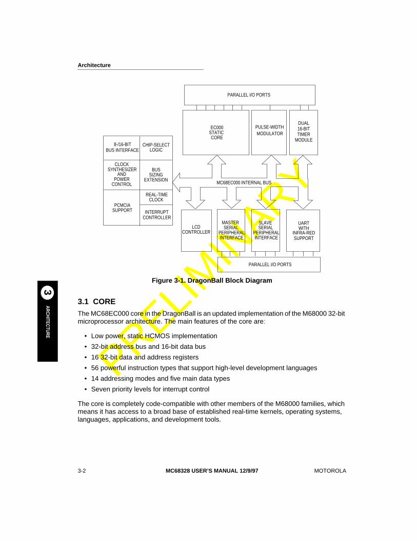
To improve total system throughput and reduce component count, board size, and cost of system implementation, the DragonBall combines a powerful MC68EC000 processor with intelligent peripheral modules and a typical system interface logic. The architecture of the DragonBall consists of the following blocks:
• EC000 core
• Chip-select logic and bus interface
• Clock synthesizer and power management
• Interrupt controller
• Parallel general-purpose I/O ports
• Timers
• Low-power stop logic
• LCD controller
• UART
• Real-time clock
• Pulse-width modulator
• Serial peripheral interface
This manual assumes you are familiar with 68K architecture. If you are not, get a copy of the
M68000 User’s Manual
(part number M68000UM/AD) and
M68000 Programmer’s Reference Manual
(part number M68000PM/AD) from your local Motorola sales office.
Architecture
3-2
MC68328 USER’S MANUAL 12/9/97
MOTOROLA
ARCHITECTURE
3
PRELIM
INARY
3.1 CORE
The MC68EC000 core in the DragonBall is an updated implementation of the M68000 32-bit microprocessor architecture. The main features of the core are:
• Low power, static HCMOS implementation
• 32-bit address bus and 16-bit data bus
• 16 32-bit data and address registers
• 56 powerful instruction types that support high-level development languages
• 14 addressing modes and five main data types
• Seven priority levels for interrupt control
The core is completely code-compatible with other members of the M68000 families, which means it has access to a broad base of established real-time kernels, operating systems, languages, applications, and development tools.
Figure 3-1. DragonBall Block Diagram
DUAL16-BITTIMER
MODULE
PULSE-WIDTHMODULATOR
EC000STATIC CORE
UARTWITH
INFRA-REDSUPPORT
SLAVEMASTERSERIAL LCD
CONTROLLER
CHIP-SELECTLOGIC
REAL-TIME
INTERRUPTCONTROLLER
PCMCIASUPPORT
CLOCKSYNTHESIZER
ANDPOWER
CONTROL
BUS
MC68EC000 INTERNAL BUS
8-/16-BITBUS INTERFACE
PARALLEL I/O PORTS
PARALLEL I/O PORTS
CLOCK
PERIPHERALINTERFACE
SERIAL PERIPHERALINTERFACE
SIZING EXTENSION
Architecture
MOTOROLA
MC68328 USER’S MANUAL 12/9/97
3-3
ARCH
ITEC
TURE
3
PRELIM
INARY
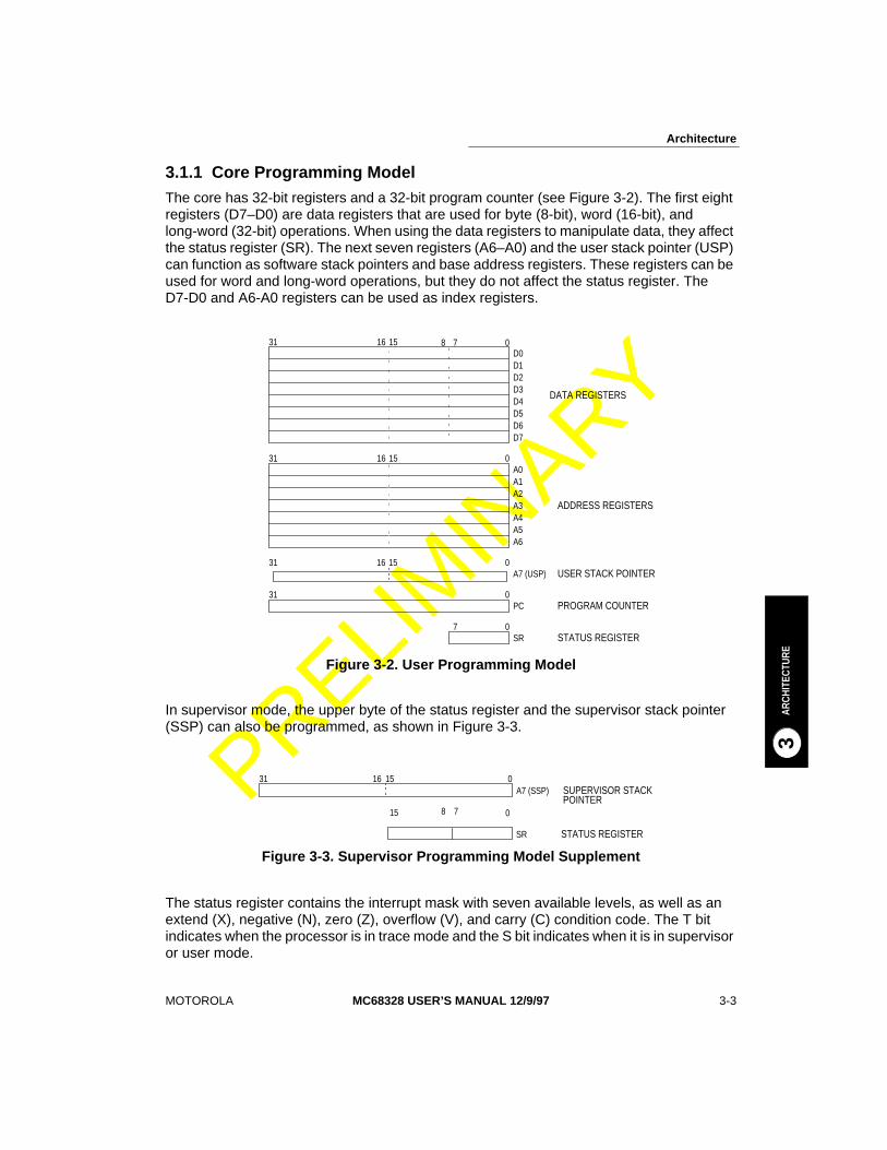
3.1.1 Core Programming Model
The core has 32-bit registers and a 32-bit program counter (see Figure 3-2). The first eight registers (D7–D0) are data registers that are used for byte (8-bit), word (16-bit), and long-word (32-bit) operations. When using the data registers to manipulate data, they affect the status register (SR). The next seven registers (A6–A0) and the user stack pointer (USP) can function as software stack pointers and base address registers. These registers can be used for word and long-word operations, but they do not affect the status register. The D7-D0 and A6-A0 registers can be used as index registers.
In supervisor mode, the upper byte of the status register and the supervisor stack pointer (SSP) can also be programmed, as shown in Figure 3-3.
The status register contains the interrupt mask with seven available levels, as well as an extend (X), negative (N), zero (Z), overflow (V), and carry (C) condition code. The T bit indicates when the processor is in trace mode and the S bit indicates when it is in supervisor or user mode.
Figure 3-2. User Programming Model
Figure 3-3. Supervisor Programming Model Supplement
DATA REGISTERS
ADDRESS REGISTERS
31 16 15 8
7
0
USER STACK POINTERA7 (USP)
D0D1D2D3D4D5D6D7
A0A1A2A3A4A5A6
0151631
31 16 15 0
31 0
0
PC PROGRAM COUNTER
STATUS REGISTERSR
7
SUPERVISOR STACKA7 (SSP)31 16 15 0
POINTER15 0 78
SR STATUS REGISTER
Architecture
3-4
MC68328 USER’S MANUAL 12/9/97
MOTOROLA
ARCHITECTURE
3
PRELIM
INARY
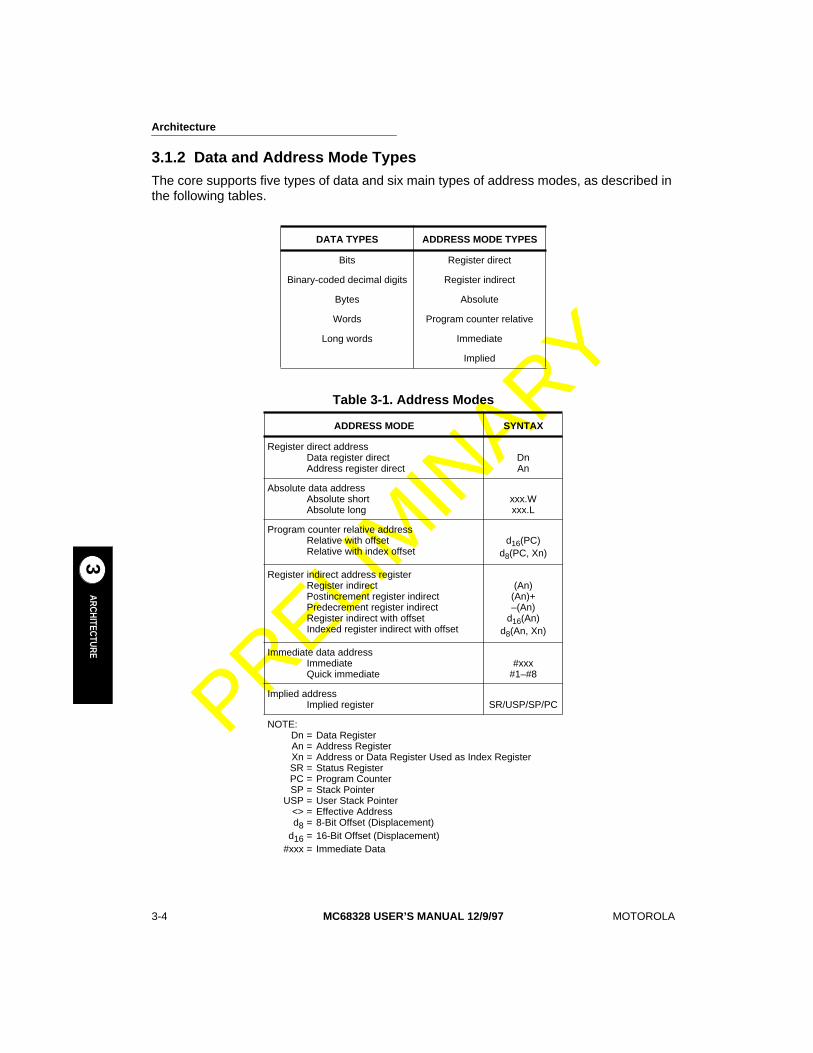
3.1.2 Data and Address Mode Types
The core supports five types of data and six main types of address modes, as described in the following tables.
DATA TYPES ADDRESS MODE TYPES
Bits Register direct
Binary-coded decimal digits Register indirect
Bytes Absolute
Words Program counter relative
Long words Immediate
Implied
Table 3-1. Address Modes
ADDRESS MODE SYNTAX
Register direct address Data register directAddress register direct
DnAn
Absolute data address Absolute shortAbsolute long
xxx.Wxxx.L
Program counter relative address Relative with offsetRelative with index offset
d
16
(PC)d
8
(PC, Xn)
Register indirect address registerRegister indirectPostincrement register indirectPredecrement register indirectRegister indirect with offsetIndexed register indirect with offset
(An)(An)+–(An)
d
16
(An)d
8
(An, Xn)
Immediate data address ImmediateQuick immediate
#xxx#1–#8
Implied address Implied register SR/USP/SP/PC
NOTE:Dn = Data RegisterAn = Address RegisterXn = Address or Data Register Used as Index RegisterSR = Status RegisterPC = Program CounterSP = Stack Pointer
USP = User Stack Pointer<> = Effective Addressd
8
= 8-Bit Offset (Displacement)d
16
= 16-Bit Offset (Displacement)#xxx = Immediate Data
Architecture
MOTOROLA
MC68328 USER’S MANUAL 12/9/97
3-5
ARCH
ITEC
TURE
3
PRELIM
INARY
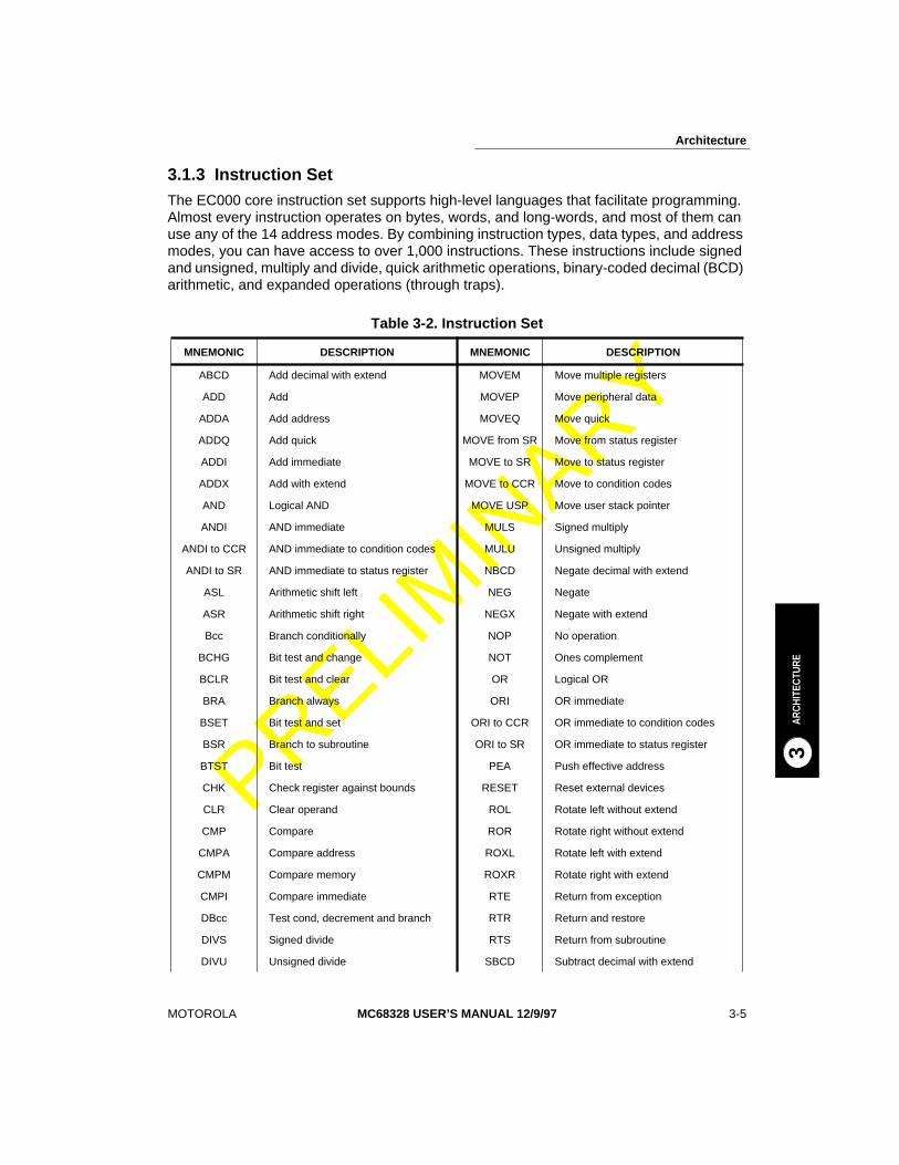
3.1.3 Instruction Set
The EC000 core instruction set supports high-level languages that facilitate programming. Almost every instruction operates on bytes, words, and long-words, and most of them can use any of the 14 address modes. By combining instruction types, data types, and address modes, you can have access to over 1,000 instructions. These instructions include signed and unsigned, multiply and divide, quick arithmetic operations, binary-coded decimal (BCD) arithmetic, and expanded operations (through traps).
Table 3-2. Instruction Set
MNEMONIC DESCRIPTION MNEMONIC DESCRIPTION
ABCD Add decimal with extend MOVEM Move multiple registers
ADD Add MOVEP Move peripheral data
ADDA Add address MOVEQ Move quick
ADDQ Add quick MOVE from SR Move from status register
ADDI Add immediate MOVE to SR Move to status register
ADDX Add with extend MOVE to CCR Move to condition codes
AND Logical AND MOVE USP Move user stack pointer
ANDI AND immediate MULS Signed multiply
ANDI to CCR AND immediate to condition codes MULU Unsigned multiply
ANDI to SR AND immediate to status register NBCD Negate decimal with extend
ASL Arithmetic shift left NEG Negate
ASR Arithmetic shift right NEGX Negate with extend
Bcc Branch conditionally NOP No operation
BCHG Bit test and change NOT Ones complement
BCLR Bit test and clear OR Logical OR
BRA Branch always ORI OR immediate
BSET Bit test and set ORI to CCR OR immediate to condition codes
BSR Branch to subroutine ORI to SR OR immediate to status register
BTST Bit test PEA Push effective address
CHK Check register against bounds RESET Reset external devices
CLR Clear operand ROL Rotate left without extend
CMP Compare ROR Rotate right without extend
CMPA Compare address ROXL Rotate left with extend
CMPM Compare memory ROXR Rotate right with extend
CMPI Compare immediate RTE Return from exception
DBcc Test cond, decrement and branch RTR Return and restore
DIVS Signed divide RTS Return from subroutine
DIVU Unsigned divide SBCD Subtract decimal with extend
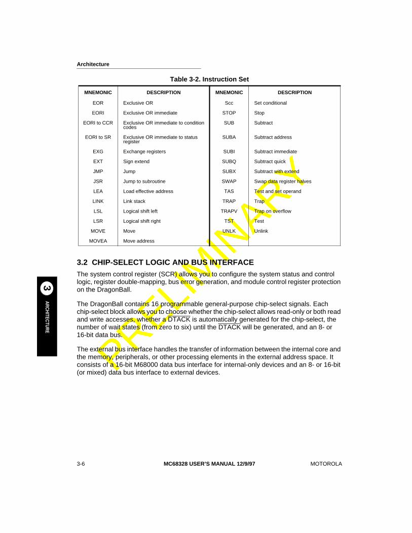
Architecture
3-6
MC68328 USER’S MANUAL 12/9/97
MOTOROLA
ARCHITECTURE
3
PRELIM
INARY
3.2 CHIP-SELECT LOGIC AND BUS INTERFACE
The system control register (SCR) allows you to configure the system status and control logic, register double-mapping, bus error generation, and module control register protection on the DragonBall.
The DragonBall contains 16 programmable general-purpose chip-select signals. Each chip-select block allows you to choose whether the chip-select allows read-only or both read and write accesses, whether a DTACK is automatically generated for the chip-select, the number of wait states (from zero to six) until the DTACK will be generated, and an 8- or 16-bit data bus.
The external bus interface handles the transfer of information between the internal core and the memory, peripherals, or other processing elements in the external address space. It consists of a 16-bit M68000 data bus interface for internal-only devices and an 8- or 16-bit (or mixed) data bus interface to external devices.
EOR Exclusive OR Scc Set conditional
EORI Exclusive OR immediate STOP Stop
EORI to CCR Exclusive OR immediate to condition codes
SUB Subtract
EORI to SR Exclusive OR immediate to status register
SUBA Subtract address
EXG Exchange registers SUBI Subtract immediate
EXT Sign extend SUBQ Subtract quick
JMP Jump SUBX Subtract with extend
JSR Jump to subroutine SWAP Swap data register halves
LEA Load effective address TAS Test and set operand
LINK Link stack TRAP Trap
LSL Logical shift left TRAPV Trap on overflow
LSR Logical shift right TST Test
MOVE Move UNLK Unlink
MOVEA Move address
Table 3-2. Instruction Set
MNEMONIC DESCRIPTION MNEMONIC DESCRIPTION
Architecture
MOTOROLA
MC68328 USER’S MANUAL 12/9/97
3-7
ARCH
ITEC
TURE
3
PRELIM
INARY
3.3 PLL CLOCK SYNTHESIZER AND POWER CONTROL
The clock synthesizer can operate with either an external crystal or an external oscillator using an internal phase-locked loop (PLL). An external clock can also be used to directly drive the clock signal at the operational frequency.
You can save power on the DragonBall by turning off peripherals that are not being used, reducing processor clock speed, or disabling the processor altogether. An interrupt at the interrupt controller logic that runs during low-power mode allows you to wake up from this mode. Programmable interrupt sources cause the system to wake up. On-chip peripherals can initiate a wake-up from doze mode and the external interrupts and real-time clock can wake up the core from sleep mode.
3.4 INTERRUPT CONTROLLER
The interrupt controller prioritizes internal and external interrupt requests and generates a vector number during the CPU interrupt-acknowledge cycle. Interrupt nesting is also provided so that an interrupt service routine of a lower priority interrupt may be suspended by a higher priority interrupt request. The on-chip interrupt controller has the following features:
• Prioritized interrupts
• Fully nested interrupt environment
• Programmable vector generation
• Unique vector number generated for each interrupt level
• Interrupt masking
• Wake-up interrupt masking
3.5 PARALLEL GENERAL-PURPOSE I/O PORTS
The DragonBall supports up to 77 general-purpose I/O ports that you can configure as general-purpose I/O pins or dedicated peripheral interface pins. Each pin can be independently programmed as a general-purpose I/O pin even when other pins related to that on-chip peripheral are used as dedicated pins. If all the pins for a particular peripheral are configured as general-purpose I/O, the peripheral will still operate normally.
3.6 TIMERS
The software watchdog timer protects against system failures by providing a way for you to escape from unexpected input conditions, external events, or programming errors. Once started, the software watchdog timer must be cleared by software on a regular basis so that it never reaches its time-out value. When it does reach its time-out value, the watchdog timer assumes that a system failure has occurred and the software watchdog logic resets or interrupts the core.
Architecture
3-8
MC68328 USER’S MANUAL 12/9/97
MOTOROLA
ARCHITECTURE
3
PRELIM
INARY
3.7 LCD CONTROLLER
The LCD controller is used to display data on an LCD module. It fetches display data from memory and provides control signals, frame line pulse, clocks, and data to the LCD module. It supports monochrome STN LCD modules with a maximum of four grayscale levels with frame rate control. System RAM can be used as display memory and DMA frees the CPU from panel refresh responsibilities.
3.8 UART
The UART communicates with external devices with a standard asynchronous protocol at baud rates from 300bps to 115.2kpbs. The UART provides the pulses to directly drive standard IrDA transceivers.
3.9 REAL-TIME CLOCK
A The real-time clock provides time-of-day with one-second resolution. It uses the crystal (either 32.76 or 38.4kHz) as a clock source to keep proper time. It keeps time as long as power is applied to the chip, which can be in sleep or doze mode.
Architecture
MOTOROLA
MC68328 USER’S MANUAL 12/9/97
3-9
ARCH
ITEC
TURE
3
PRELIM
INARY
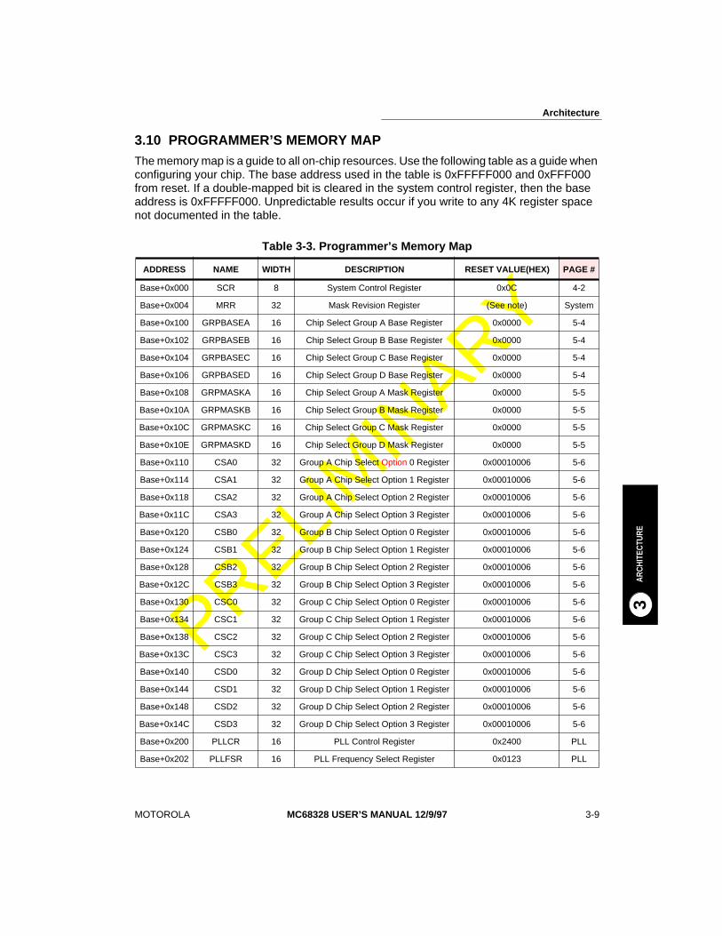
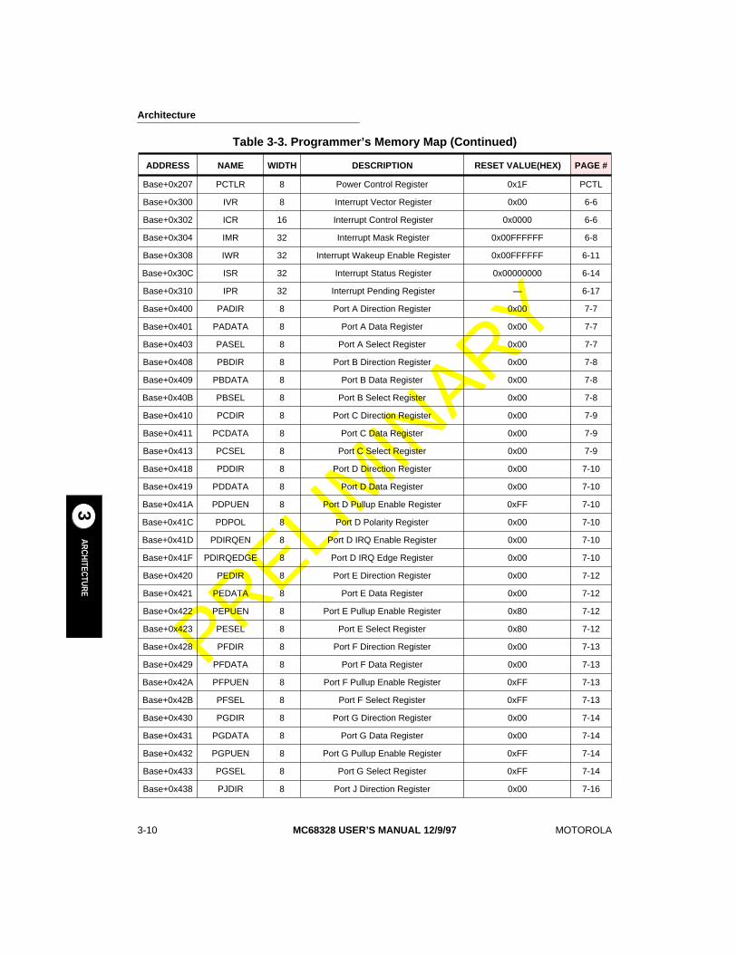
3.10 PROGRAMMER’S MEMORY MAP
The memory map is a guide to all on-chip resources. Use the following table as a guide when configuring your chip. The base address used in the table is 0xFFFFF000 and 0xFFF000 from reset. If a double-mapped bit is cleared in the system control register, then the base address is 0xFFFFF000. Unpredictable results occur if you write to any 4K register space not documented in the table.
Table 3-3. Programmer’s Memory Map
ADDRESS NAME WIDTH DESCRIPTION RESET VALUE(HEX) PAGE #
Base+0x000 SCR 8 System Control Register 0x0C 4-2
Base+0x004 MRR 32 Mask Revision Register (See note) System
Base+0x100 GRPBASEA 16 Chip Select Group A Base Register 0x0000 5-4
Base+0x102 GRPBASEB 16 Chip Select Group B Base Register 0x0000 5-4
Base+0x104 GRPBASEC 16 Chip Select Group C Base Register 0x0000 5-4
Base+0x106 GRPBASED 16 Chip Select Group D Base Register 0x0000 5-4
Base+0x108 GRPMASKA 16 Chip Select Group A Mask Register 0x0000 5-5
Base+0x10A GRPMASKB 16 Chip Select Group B Mask Register 0x0000 5-5
Base+0x10C GRPMASKC 16 Chip Select Group C Mask Register 0x0000 5-5
Base+0x10E GRPMASKD 16 Chip Select Group D Mask Register 0x0000 5-5
Base+0x110 CSA0 32 Group A Chip Select Option 0 Register 0x00010006 5-6
Base+0x114 CSA1 32 Group A Chip Select Option 1 Register 0x00010006 5-6
Base+0x118 CSA2 32 Group A Chip Select Option 2 Register 0x00010006 5-6
Base+0x11C CSA3 32 Group A Chip Select Option 3 Register 0x00010006 5-6
Base+0x120 CSB0 32 Group B Chip Select Option 0 Register 0x00010006 5-6
Base+0x124 CSB1 32 Group B Chip Select Option 1 Register 0x00010006 5-6
Base+0x128 CSB2 32 Group B Chip Select Option 2 Register 0x00010006 5-6
Base+0x12C CSB3 32 Group B Chip Select Option 3 Register 0x00010006 5-6
Base+0x130 CSC0 32 Group C Chip Select Option 0 Register 0x00010006 5-6
Base+0x134 CSC1 32 Group C Chip Select Option 1 Register 0x00010006 5-6
Base+0x138 CSC2 32 Group C Chip Select Option 2 Register 0x00010006 5-6
Base+0x13C CSC3 32 Group C Chip Select Option 3 Register 0x00010006 5-6
Base+0x140 CSD0 32 Group D Chip Select Option 0 Register 0x00010006 5-6
Base+0x144 CSD1 32 Group D Chip Select Option 1 Register 0x00010006 5-6
Base+0x148 CSD2 32 Group D Chip Select Option 2 Register 0x00010006 5-6
Base+0x14C CSD3 32 Group D Chip Select Option 3 Register 0x00010006 5-6
Base+0x200 PLLCR 16 PLL Control Register 0x2400 PLL
Base+0x202 PLLFSR 16 PLL Frequency Select Register 0x0123 PLL
Architecture
3-10
MC68328 USER’S MANUAL 12/9/97
MOTOROLA
ARCHITECTURE
3
PRELIM
INARY
Base+0x207 PCTLR 8 Power Control Register 0x1F PCTL
Base+0x300 IVR 8 Interrupt Vector Register 0x00 6-6
Base+0x302 ICR 16 Interrupt Control Register 0x0000 6-6
Base+0x304 IMR 32 Interrupt Mask Register 0x00FFFFFF 6-8
Base+0x308 IWR 32 Interrupt Wakeup Enable Register 0x00FFFFFF 6-11
Base+0x30C ISR 32 Interrupt Status Register 0x00000000 6-14
Base+0x310 IPR 32 Interrupt Pending Register — 6-17
Base+0x400 PADIR 8 Port A Direction Register 0x00 7-7
Base+0x401 PADATA 8 Port A Data Register 0x00 7-7
Base+0x403 PASEL 8 Port A Select Register 0x00 7-7
Base+0x408 PBDIR 8 Port B Direction Register 0x00 7-8
Base+0x409 PBDATA 8 Port B Data Register 0x00 7-8
Base+0x40B PBSEL 8 Port B Select Register 0x00 7-8
Base+0x410 PCDIR 8 Port C Direction Register 0x00 7-9
Base+0x411 PCDATA 8 Port C Data Register 0x00 7-9
Base+0x413 PCSEL 8 Port C Select Register 0x00 7-9
Base+0x418 PDDIR 8 Port D Direction Register 0x00 7-10
Base+0x419 PDDATA 8 Port D Data Register 0x00 7-10
Base+0x41A PDPUEN 8 Port D Pullup Enable Register 0xFF 7-10
Base+0x41C PDPOL 8 Port D Polarity Register 0x00 7-10
Base+0x41D PDIRQEN 8 Port D IRQ Enable Register 0x00 7-10
Base+0x41F PDIRQEDGE 8 Port D IRQ Edge Register 0x00 7-10
Base+0x420 PEDIR 8 Port E Direction Register 0x00 7-12
Base+0x421 PEDATA 8 Port E Data Register 0x00 7-12
Base+0x422 PEPUEN 8 Port E Pullup Enable Register 0x80 7-12
Base+0x423 PESEL 8 Port E Select Register 0x80 7-12
Base+0x428 PFDIR 8 Port F Direction Register 0x00 7-13
Base+0x429 PFDATA 8 Port F Data Register 0x00 7-13
Base+0x42A PFPUEN 8 Port F Pullup Enable Register 0xFF 7-13
Base+0x42B PFSEL 8 Port F Select Register 0xFF 7-13
Base+0x430 PGDIR 8 Port G Direction Register 0x00 7-14
Base+0x431 PGDATA 8 Port G Data Register 0x00 7-14
Base+0x432 PGPUEN 8 Port G Pullup Enable Register 0xFF 7-14
Base+0x433 PGSEL 8 Port G Select Register 0xFF 7-14
Base+0x438 PJDIR 8 Port J Direction Register 0x00 7-16
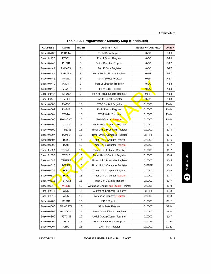
Table 3-3. Programmer’s Memory Map (Continued)
ADDRESS NAME WIDTH DESCRIPTION RESET VALUE(HEX) PAGE #
Architecture
MOTOROLA
MC68328 USER’S MANUAL 12/9/97
3-11
ARCH
ITEC
TURE
3
PRELIM
INARY
Base+0x439 PJDATA 8 Port J Data Register 0x00 7-16
Base+0x43B PJSEL 8 Port J Select Register 0x00 7-16
Base+0x440 PKDIR 8 Port K Direction Register 0x00 7-17
Base+0x441 PKDATA 8 Port K Data Register 0x00 7-17
Base+0x442 PKPUEN 8 Port K Pullup Enable Register 0x3F 7-17
Base+0x443 PKSEL 8 Port K Select Register 0x3F 7-17
Base+0x448 PMDIR 8 Port M Direction Register 0x00 7-18
Base+0x449 PMDATA 8 Port M Data Register 0x00 7-18
Base+0x44A PMPUEN 8 Port M Pullup Enable Register 0xFF 7-18
Base+0x44B PMSEL 8 Port M Select Register 0x02 7-18
Base+0x500 PWMC 16 PWM Control Register 0x0000 PWM
Base+0x502 PWMP 16 PWM Period Register 0x0000 PWM
Base+0x504 PWMW 16 PWM Width Register 0x0000 PWM
Base+0x506 PWMCNT 16 PWM Counter Register 0x0000 PWM
Base+0x600 TCTL1 16 Timer Unit 1 Control Register 0x0000 10-4
Base+0x602 TPRER1 16 Timer Unit 1 Prescalar Register 0x0000 10-5
Base+0x604 TCMP1 16 Timer Unit 1 Compare Register 0xFFFF 10-6
Base+0x606 TCR1 16 Timer Unit 1 Capture Register 0x0000 10-6
Base+0x608 TCN1 16 Timer Unit 1 Counter Register 0x0000 10-7
Base+0x60A TSTAT1 16 Timer Unit 1 Status Register 0x0000 10-7
Base+0x60C TCTL2 16 Timer Unit 2 Control Register 0x0000 10-4
Base+0x60E TPREP2 16 Timer Unit 2 Prescaler Register 0x0000 10-5
Base+0x610 TCMP2 16 Timer Unit 2 Compare Register 0xFFFF 10-6
Base+0x612 TCR2 16 Timer Unit 2 Capture Register 0x0000 10-6
Base+0x614 TCN2 16 Timer Unit 2 Counter Register 0x0000 10-7
Base+0x616 TSTAT2 16 Timer Unit 2 Status Register 0x0000 10-7
Base+0x618 WCSR 16 Watchdog Control and Status Register 0x0001 10-9
Base+0x61A WRR 16 Watchdog Compare Register 0xFFFF 10-8
Base+0x61C WCN 16 Watchdog Counter Register 0x0000 10-8
Base+0x700 SPISR 16 SPIS Register 0x0000 SPIS
Base+0x800 SPIMDATA 16 SPIM Data Register 0x0000 SPIM
Base+0x802 SPIMCONT 16 SPIM Control/Status Register 0x0000 SPIM
Base+0x900 USTCNT 16 UART Status/Control Register 0x0000 11-7
Base+0x902 UBAUD 16 UART Baud Control Register 0x003F 11-10
Base+0x904 URX 16 UART RX Register 0x0000 11-12
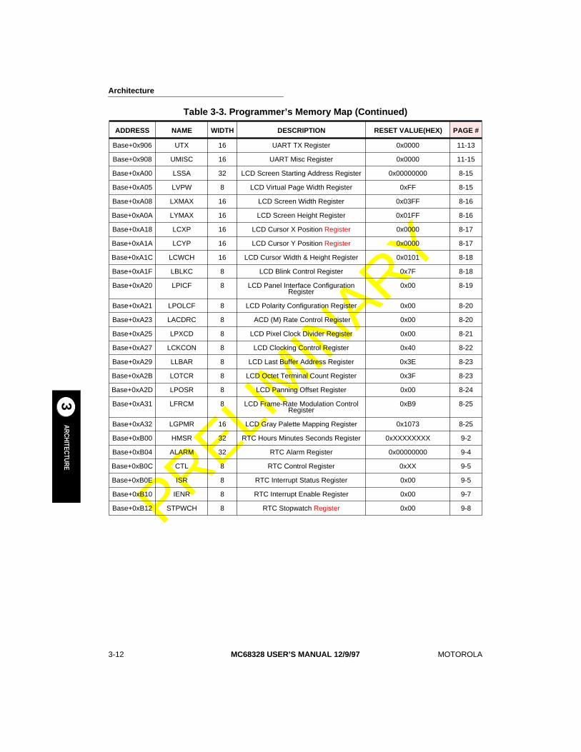
Table 3-3. Programmer’s Memory Map (Continued)
ADDRESS NAME WIDTH DESCRIPTION RESET VALUE(HEX) PAGE #
Architecture
3-12
MC68328 USER’S MANUAL 12/9/97
MOTOROLA
ARCHITECTURE
3
PRELIM
INARY
Base+0x906 UTX 16 UART TX Register 0x0000 11-13
Base+0x908 UMISC 16 UART Misc Register 0x0000 11-15
Base+0xA00 LSSA 32 LCD Screen Starting Address Register 0x00000000 8-15
Base+0xA05 LVPW 8 LCD Virtual Page Width Register 0xFF 8-15
Base+0xA08 LXMAX 16 LCD Screen Width Register 0x03FF 8-16
Base+0xA0A LYMAX 16 LCD Screen Height Register 0x01FF 8-16
Base+0xA18 LCXP 16 LCD Cursor X Position Register 0x0000 8-17
Base+0xA1A LCYP 16 LCD Cursor Y Position Register 0x0000 8-17
Base+0xA1C LCWCH 16 LCD Cursor Width & Height Register 0x0101 8-18
Base+0xA1F LBLKC 8 LCD Blink Control Register 0x7F 8-18
Base+0xA20 LPICF 8 LCD Panel Interface ConfigurationRegister
0x00 8-19
Base+0xA21 LPOLCF 8 LCD Polarity Configuration Register 0x00 8-20
Base+0xA23 LACDRC 8 ACD (M) Rate Control Register 0x00 8-20
Base+0xA25 LPXCD 8 LCD Pixel Clock Divider Register 0x00 8-21
Base+0xA27 LCKCON 8 LCD Clocking Control Register 0x40 8-22
Base+0xA29 LLBAR 8 LCD Last Buffer Address Register 0x3E 8-23
Base+0xA2B LOTCR 8 LCD Octet Terminal Count Register 0x3F 8-23
Base+0xA2D LPOSR 8 LCD Panning Offset Register 0x00 8-24
Base+0xA31 LFRCM 8 LCD Frame-Rate Modulation Control Register
0xB9 8-25
Base+0xA32 LGPMR 16 LCD Gray Palette Mapping Register 0x1073 8-25
Base+0xB00 HMSR 32 RTC Hours Minutes Seconds Register 0xXXXXXXXX 9-2
Base+0xB04 ALARM 32 RTC Alarm Register 0x00000000 9-4
Base+0xB0C CTL 8 RTC Control Register 0xXX 9-5
Base+0xB0E ISR 8 RTC Interrupt Status Register 0x00 9-5
Base+0xB10 IENR 8 RTC Interrupt Enable Register 0x00 9-7
Base+0xB12 STPWCH 8 RTC Stopwatch Register 0x00 9-8
Table 3-3. Programmer’s Memory Map (Continued)
ADDRESS NAME WIDTH DESCRIPTION RESET VALUE(HEX) PAGE #
MOTOROLA
MC68328 USER’S MANUAL 12/9/97
4-1
SYST
EM C
ONT
ROL
4
PRELIM
INARY
SECTION 4SYSTEM CONTROL
The DragonBall microprocessor contains a system control register that enables the system software to customize the following functions:
• Access permission from the internal peripheral registers
• Address space of the internal peripheral registers
• Bus timeout control and status (bus-error generator)
4.1 OPERATION
The on-chip resources use a reserved 4,096-byte block of address space for their registers. This block is double-mapped to two locations—0xFFFFF000 (24-bit) and 0xFFF000 (32-bit) —at reset. The DMAP bit in the system control register disables double-mapping in a 32-bit system. If you clear this bit, the on-chip peripheral registers appear only at the top of the 4G address range starting at 0xFFFFF000.
The system control register allows you to control system operation functions like bus interface and hardware watchdog protection. It contains status bits that allow exception handler code to investigate the cause of exceptions and resets. The hardware watchdog (bus timeout monitor) and the software watchdog timer provide system protection. The hardware watchdog provides a bus monitor that causes a bus error when a bus cycle is not terminated by the DTACK signal before 128 clock cycles have elapsed.
The bus error timeout logic consists of a watchdog counter that, when enabled, begins to count clock cycles as the AS pin is asserted for internal or external bus accesses. The negation of AS normally terminates the count, but if the count reaches terminal count before AS is negated, BERR is asserted until AS is negated. The bus error timeout logic uses one control bit and one status bit in the system control register. The BETO bit in the system control register is set after a bus timeout, which could be caused by a write-protect violation.
The software watchdog timer resets the DragonBall if enabled and not cleared or disabled before reaching terminal count. The software watchdog timer is enabled at reset. For information about timer operation, see
Section 8.3 Software Watchdog Timer
.
System Control
4-2
MC68328 USER’S MANUAL 12/9/97
MOTOROLA
MO
DULESYSTEM
CONTRO
L
4
PRELIM
INARY
4.1.1 System Control Register
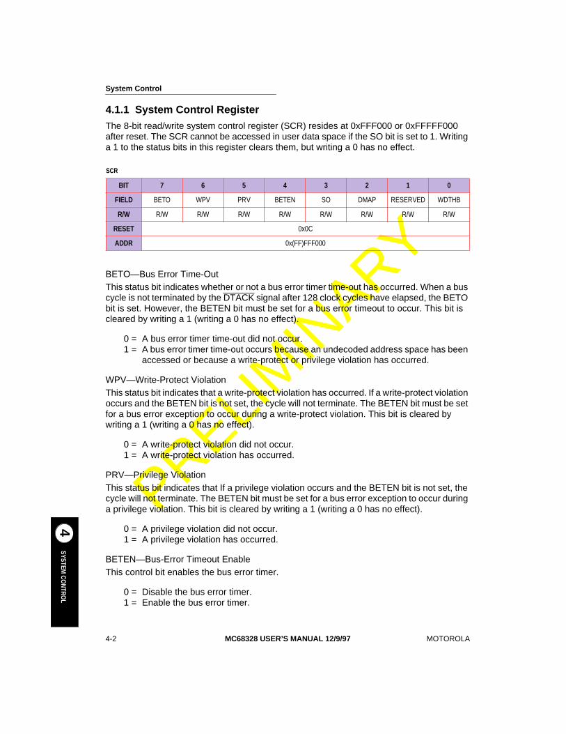
The 8-bit read/write system control register (SCR) resides at 0xFFF000 or 0xFFFFF000 after reset. The SCR cannot be accessed in user data space if the SO bit is set to 1. Writing a 1 to the status bits in this register clears them, but writing a 0 has no effect.
BETO—Bus Error Time-OutThis status bit indicates whether or not a bus error timer time-out has occurred. When a bus cycle is not terminated by the DTACK signal after 128 clock cycles have elapsed, the BETO bit is set. However, the BETEN bit must be set for a bus error timeout to occur. This bit is cleared by writing a 1 (writing a 0 has no effect).
0 = A bus error timer time-out did not occur.1 = A bus error timer time-out occurs because an undecoded address space has been
accessed or because a write-protect or privilege violation has occurred.
WPV—Write-Protect ViolationThis status bit indicates that a write-protect violation has occurred. If a write-protect violation occurs and the BETEN bit is not set, the cycle will not terminate. The BETEN bit must be set for a bus error exception to occur during a write-protect violation. This bit is cleared by writing a 1 (writing a 0 has no effect).
0 = A write-protect violation did not occur.1 = A write-protect violation has occurred.
PRV—Privilege ViolationThis status bit indicates that If a privilege violation occurs and the BETEN bit is not set, the cycle will not terminate. The BETEN bit must be set for a bus error exception to occur during a privilege violation. This bit is cleared by writing a 1 (writing a 0 has no effect).
0 = A privilege violation did not occur.1 = A privilege violation has occurred.
BETEN—Bus-Error Timeout EnableThis control bit enables the bus error timer.
0 = Disable the bus error timer.1 = Enable the bus error timer.
SCR
BIT 7 6 5 4 3 2 1 0
FIELD
BETO WPV PRV BETEN SO DMAP RESERVED WDTHB
R/W
R/W R/W R/W R/W R/W R/W R/W R/W
RESET
0x0C
ADDR
0x(FF)FFF000
System Control
MOTOROLA
MC68328 USER’S MANUAL 12/9/97
4-3
SYST
EM C
ONT
ROL
4
PRELIM
INARY
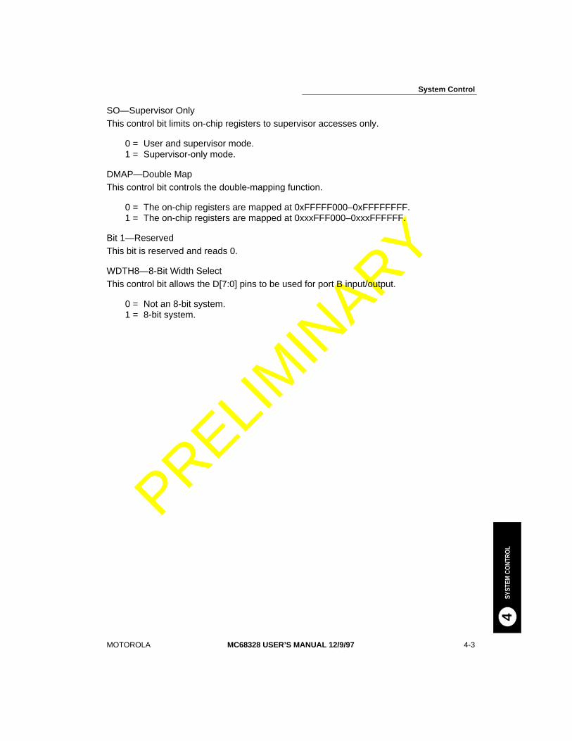
SO—Supervisor OnlyThis control bit limits on-chip registers to supervisor accesses only.
0 = User and supervisor mode.1 = Supervisor-only mode.
DMAP—Double MapThis control bit controls the double-mapping function.
0 = The on-chip registers are mapped at 0xFFFFF000–0xFFFFFFFF.1 = The on-chip registers are mapped at 0xxxFFF000–0xxxFFFFFF.
Bit 1—ReservedThis bit is reserved and reads 0.
WDTH8—8-Bit Width SelectThis control bit allows the D[7:0] pins to be used for port B input/output.
0 = Not an 8-bit system.1 = 8-bit system.

System Control
4-4
MC68328 USER’S MANUAL 12/9/97
MOTOROLA
MO
DULESYSTEM
CONTRO
L
4
PRELIM
INARY
MOTOROLA
MC68328 USER’S MANUAL 12/9/97
5-1
CHIP
-SEL
ECT
LOG
IC
5
PRELIM
INARY
SECTION 5CHIP-SELECT LOGIC
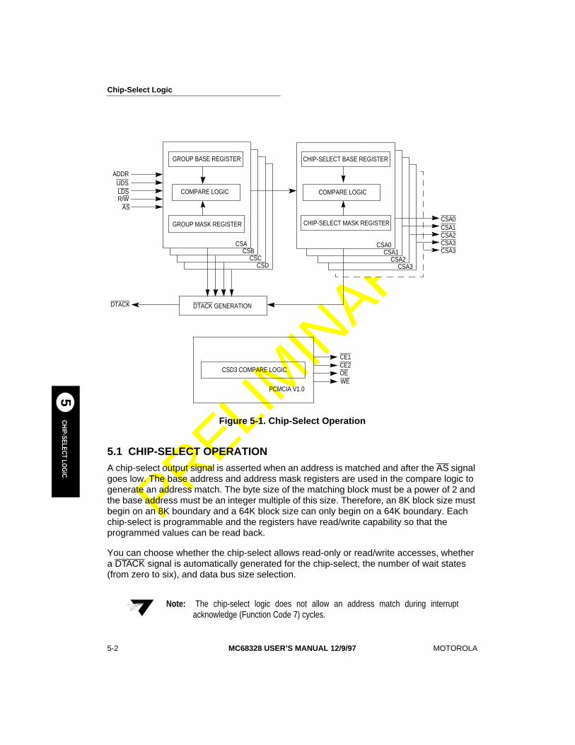
The DragonBall microprocessor contains 16 general-purpose, programmable, chip-select signals, which are arranged in four groups of four. Among them, there are two special-purpose chip-select signals—CSA0 and CSD3. The CSA0 signal is special in that it is also a boot device chip-select. From reset, all the addresses are mapped to CSA0 until group-base address A is programmed and the V bit is set. From that point on, CSA0 does not decode globally and it is only asserted when decoded from the programming information in the group-base address register, group-base address mask register, chip-select base register, and chip-select option register. The CSD3 signal is also special because it is associated with the PCMCIA support logic. When CSD3 is asserted, the PCMCIA control signals are asserted. For each memory area, you can define an internally generated cycle-termination signal, called DTACK, with a programmable number of wait states. This feature saves board space that would otherwise be used for cycle-termination logic.
The 16 general-purpose chip-selects allow different classes of devices and memory to be used in a system without external decode or wait-state generation logic. A typical configuration would be an 8-bit EPROM, a fast 16-bit SRAM, four simple I/O peripherals, and a nonvolatile flash memory. See
Section 16 Applications and Design Examples
for more information.
Chip-Select Logic
5-2
MC68328 USER’S MANUAL 12/9/97
MOTOROLA
MO
DULECHIP-SELECT LO
GIC
5
PRELIM
INARY
5.1 CHIP-SELECT OPERATION
A chip-select output signal is asserted when an address is matched and after the AS signal goes low. The base address and address mask registers are used in the compare logic to generate an address match. The byte size of the matching block must be a power of 2 and the base address must be an integer multiple of this size. Therefore, an 8K block size must begin on an 8K boundary and a 64K block size can only begin on a 64K boundary. Each chip-select is programmable and the registers have read/write capability so that the programmed values can be read back.
You can choose whether the chip-select allows read-only or read/write accesses, whether a DTACK signal is automatically generated for the chip-select, the number of wait states (from zero to six), and data bus size selection.
Figure 5-1. Chip-Select Operation
Note:
The chip-select logic does not allow an address match during interruptacknowledge (Function Code 7) cycles.
DTACK GENERATION
CSA0CSA1CSA2CSA3
CSD3 COMPARE LOGIC
PCMCIA V1.0
CE1CE2OEWE
DTACK
GROUP BASE REGISTER
COMPARE LOGIC
GROUP MASK REGISTER
CSA
ADDRUDSLDSR/W
AS
CHIP-SELECT BASE REGISTER
COMPARE LOGIC
CHIP-SELECT MASK REGISTER
CSA0CSB
CSCCSD
CSA1CSA2
CSA3
CSA3
Chip-Select Logic
MOTOROLA
MC68328 USER’S MANUAL 12/9/97
5-3
CHIP
-SEL
ECT
LOG
IC
5
PRELIM
INARY
5.1.1 Programmable Data Bus Size
Each chip-select can be configured to address an 8- or 16-bit space. You can mix 16- and 8-bit contiguous address memory devices on a 16-bit data bus system. If the core performs a 16-bit data transfer in an 8-bit memory space, then two 8-bit cycles will occur. However, the address and data strobes remain asserted until the end of the second 8-bit cycle. In this case, only the external core data bus upper byte (D[15:8]) is used and the least-significant bit of address (A0) increments automatically from one to the next. A0 should be ignored in 16-bit data-bus cycles even if only the upper or lower byte is being read or written. For an external peripheral that only needs an 8-bit data bus interface and does not require contiguous address locations (unused bytes on empty addresses), use a chip-select configured to a 16-bit data bus width and connect to the D[7:0] pins. This balances the load of the two data bus halves in an 8-bit system. The internal data bus is16 bits wide. All internal registers can be read or written in one zero wait-state cycle.
Each chip-select defaults to a 16-bit data bus width. The BUSW field in the chip-select option registers enable 16- and 8-bit data bus widths for each of the 16 chip-select ranges. You can select the initial bus width for the boot chip-select by placing a logic 0 or 1 on the BBUSW pin at reset to specify the width of the data bus. This allows a boot EPROM of the data bus width to be used in any given system. All external accesses that do not match one of the chip-select address ranges are assumed to be a 16-bit device. That is just one access performed for a 16-bit transfer. It can also be a 8-bit port accessed every other byte.
The boot chip-select is initialized from reset to assert in response to any address except theon-chip register space (0xXXFFF000 to 0xXXFFFFFF). This ensures that a chip-select tothe boot ROM or EPROM will fetch the reset vector and execute the initialization code, whichshould set up the chip-select ranges.
A logic 0 on the BBUSW pin makes the boot device’s data bus 8 bits wide and a logic 1 makes it 16 bits wide. At reset, the data bus port size for CSA0 and the data width of the boot ROM device are determined by the state of the BBUSW pin. The other chip-selects are initialized to be nonvalid, so they will not assert until they are programmed and the V bit is set.
Note:
If the group address and chip-select registers are programmed to overlap, theCSx signals will overlap too. Unused chip-selects must be programmed to 0 waitstates and 16 bits wide. Map them to dummy space if necessary. When you areconfiguring the chip-select signals, the core can be set to write to a read-onlylocation. This causes the CS and DTACK signals to not be asserted and theBERR signal to be asserted if a bus error timer is enabled.
Chip-Select Logic
5-4
MC68328 USER’S MANUAL 12/9/97
MOTOROLA
MO
DULECHIP-SELECT LO
GIC
5
PRELIM
INARY
5.2 PROGRAMMING MODEL
The chip-select module of the DragonBall microprocessor contains registers that you can use to control external devices, such as memory. Chip-selects do not operate until the register in a particular group of devices is initialized and the V bit is set in the corresponding group-base address register. The only exception is the CSA0 signal, which is the boot device chip-select.
5.2.1 Group Base Address Registers
There are four 16-bit group base address registers (GRPBASEA–GRPBASED) in the chip-select module (one for each chip-select group). The group base address registers and the group mask registers decode the upper address bits and the chip-select option registers decode the lower address bits. There are four chip-selects in each group. For example, in group A the chip-selects are CSA0, CSA1, CSA2, and CSA3.
GBA—Group Base Address 31–20This bit selects the starting address for the group address range. The corresponding bits in the group base mask register define the block size for the group. This field is compared to the address on the address bus to determine if the group is decoded.
Bits 1–3—ReservedThese bits are reserved.
V—ValidThis bit controls whether or not the contents of its base address register and address mask register pair are valid. The programmed chip-selects do not assert until this bit is set. A reset clears this bit in each base address register.
0 = Content is not valid.1 = Content is valid.
GRPBASEA–GRPBASED
BIT 15 14 13 12 11 10 9 8 7 6 5 4 3 2 1 0
FIELD
GBA31 GBA30 GBA29 GBA28 GBA27 GBA26 GBA25 GBA24 GBA23 GBA22 GBA21 GBA20 RESERVED V
R/W
R/W R/W R/W R/W R/W R/W R/W R/W R/W R/W R/W R/W — R/W
RESET
0x0000
ADDR
0x(FF)FFF100, 102, 104, 106
Chip-Select Logic
MOTOROLA
MC68328 USER’S MANUAL 12/9/97
5-5
CHIP
-SEL
ECT
LOG
IC
5
PRELIM
INARY
5.2.2 Group Base Address Mask Registers
The group base address mask registers (GRPMASKA–GRPMASKD) define the address comparison range for a group of devices. When the bits in this register are set to 1 the bits in the corresponding address lines (A[31:20]) compare true (“don’t care”).
GMA—Group MaskThese bits mask address A[31:20]. They are used to select the group size. For example, if all the mask bits are cleared, A[31:20] are compared against the value programmed in the group base address register. In this case, the group has a 1M space. If the GMA20 bit is set and the rest of the bits are clear, the group is selected if A[31:21] are the same as the value programmed in the group-base address register. This provides 2M of space for the group. You can decode each chip-select by comparing the lower address lines with the contents of the chip-select option registers. If the memory space for a group of devices is small, you can program the groups to a common space and use the chip-select option registers to decode the areas for each chip-select.
0 = For a match to occur, the address line must match the corresponding bit in the GRPBASEx register.
1 = The corresponding address line compares true (“don’t care”).
Bits 0–3—ReservedThese bits are reserved.
GRPMASKA–GRPMASKD
BIT 15 14 13 12 11 10 9 8 7 6 5 4 3 2 1 0
FIELD
GMA31 GMA30 GMA29 GMA28 GMA27 GMA26 GMA25 GMA24 GMA23 GMA22 GMA21 GMA20 RESERVED
R/W
R/W R/W R/W R/W R/W R/W R/W R/W R/W R/W R/W R/W —
RESET
0x0000
ADDR
0x(FF)FFF108, 10A, 10C, 10E
Chip-Select Logic
5-6
MC68328 USER’S MANUAL 12/9/97
MOTOROLA
MO
DULECHIP-SELECT LO
GIC
5
PRELIM
INARY
5.2.3 Chip-Select Option Registers
There are four 32-bit chip-select option registers (CSA0–3 and CSB0–3) in each chip-select group, one for each chip-select signal. Chip-selects in group A and B decode address lines A[23:16] for a minimum 64K space. Chip-selects in group C and D decode address lines A[23:12] for a minimum 4K space. When a group address match and a chip-select option address match occurs, a chip-select is generated.
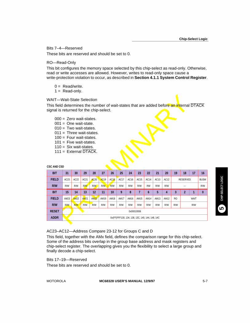
AC23–AC16—Address Compare 23-16 for Groups A and BThis field, together with the AMx field, defines the comparison range for this chip-select. Some of the address bits overlap in the group base address and mask registers and chip-select register. The overlapping gives you the flexibility to select a large group and finally decode a chip-select.
Bits 23–17—ReservedThese bits are reserved and should be set to 0.
BUSW—Bus WidthThis bit sets the bus width of the memory space selected by this chip-select.
0 = 8-bit.1 = 16-bit.
AM23–AM16—Address Mask 23-16 for Groups A and BThis field masks the corresponding bits in the ACx field.
0 = For a match to occur, the address line must match the corresponding bit in the CSAx or CSBx register.
1 = The corresponding address line compares true (“don’t care”).
CSAx AND CSBx
BIT 31 30 29 28 27 26 25 24 23 22 21 20 19 18 17 16
FIELD
AC23 AC22 AC21 AC20 AC19 AC18 AC17 AC16 RESERVED BUSW
R/W
R/W R/W R/W R/W R/W R/W R/W R/W — R/W
BIT 15 14 13 12 11 10 9 8 7 6 5 4 3 2 1 0
FIELD
AM23 AM22 AM21 AM20 AM19 AM18 AM17 AM16 RESERVED RO WAIT
R/W
R/W R/W R/W R/W R/W R/W R/W R/W — R/W R/W
RESET
0x00010006
ADDR
0x(FF)FFF110, 114, 118, 11C, 120, 124, 128, 12C
Note:
This bit is read-only for CSA0 and reflects the logic level on the BBUSW pin.
Chip-Select Logic
MOTOROLA
MC68328 USER’S MANUAL 12/9/97
5-7
CHIP
-SEL
ECT
LOG
IC
5
PRELIM
INARY
Bits 7–4—ReservedThese bits are reserved and should be set to 0.
RO—Read-OnlyThis bit configures the memory space selected by this chip-select as read-only. Otherwise, read or write accesses are allowed. However, writes to read-only space cause a write-protection violation to occur, as described in
Section 4.1.1 System Control Register
.
0 = Read/write.1 = Read-only.
WAIT—Wait-State SelectionThis field determines the number of wait-states that are added before an internal DTACK signal is returned for the chip-select.
000 = Zero wait-states.001 = One wait-state.010 = Two wait-states.011 = Three wait-states.100 = Four wait-states.101 = Five wait-states.110 = Six wait-states.111 = External DTACK.
AC23–AC12—Address Compare 23-12 for Groups C and DThis field, together with the AMx field, defines the comparison range for this chip-select. Some of the address bits overlap in the group base address and mask registers and chip-select register. The overlapping gives you the flexibility to select a large group and finally decode a chip-select.
Bits 17–19—ReservedThese bits are reserved and should be set to 0.
CSC AND CSD
BIT 31 30 29 28 27 26 25 24 23 22 21 20 19 18 17 16
FIELD
AC23 AC22 AC21 AC20 AC19 AC18 AC17 AC16 AC15 AC14 AC13 AC12 RESERVED BUSW
R/W
R/W R/W R/W R/W R/W R/W R/W R/W R/W RW R/W R/W — R/W
BIT 15 14 13 12 11 10 9 8 7 6 5 4 3 2 1 0
FIELD
AM23 AM22 AM21 AM20 AM19 AM18 AM17 AM16 AM15 AM14 AM13 AM12 RO WAIT
R/W
R/W R/W R/W R/W R/W R/W R/W R/W R/W R/W R/W R/W R/W R/W
RESET
0x00010006
ADDR
0x(FF)FFF130, 134, 138, 13C, 140, 144, 148, 14C
Chip-Select Logic
5-8
MC68328 USER’S MANUAL 12/9/97
MOTOROLA
MO
DULECHIP-SELECT LO
GIC
5
PRELIM
INARY
BUSW—Bus WidthThis bit sets the bus width of the memory space selected by this chip-select.
0 = 8-bit.1 = 16-bit.
AM23–AM12—Address Mask 23-12 for Groups C and DThis field masks the corresponding bits in the ACx field.
0 = For a match to occur, the address line must match the corresponding bit in the CSCx or CSDx register.
1 = The corresponding address line compares true (“don’t care”).
RO—Read-OnlyThis bit configures the memory space selected by this chip-select as read-only. Otherwise, read or write accesses are allowed. However, writes to read-only space cause a write-protection violation to occur, as described in
Section 4.1.1 System Control Register
.
0 = Read/write.1 = Read-only.
WAIT—Wait-State SelectionThis field determines the number of wait-states that are added before an internal DTACK signal is returned for the chip-select.
000 = Zero wait-states.001 = One wait-state.010 = Two wait-states.011 = Three wait-states.100 = Four wait-states.101 = Five wait-states.110 = Six wait-states.111 = External DTACK.
Chip-Select Logic
MOTOROLA
MC68328 USER’S MANUAL 12/9/97
5-9
CHIP
-SEL
ECT
LOG
IC
5
PRELIM
INARY
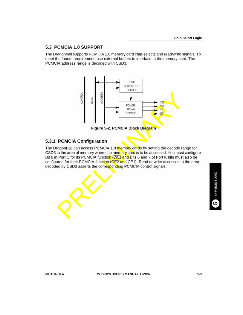
5.3 PCMCIA 1.0 SUPPORT
The Dragonball supports PCMCIA 1.0 memory card chip-selects and read/write signals. To meet the fanout requirement, use external buffers to interface to the memory card. The PCMCIA address range is decoded with CSD3.
5.3.1 PCMCIA Configuration
The DragonBall can access PCMCIA 1.0 memory cards by setting the decode range for CSD3 to the area of memory where the memory card is to be accessed. You must configure Bit 6 in Port C for its PCMCIA function (WE) and Bits 6 and 7 of Port K bits must also be configured for their PCMCIA function (CE2 and CE1). Read or write accesses to the area decoded by CSD3 asserts the corresponding PCMCIA control signals.
Figure 5-2. PCMCIA Block Diagram
CSD3CHIP-SELECT
DECODED
ATA
ADD
RES
SPCMCIASIGNALDECODE
CE1CE2OEWE
CO
NTR
OL

Chip-Select Logic
5-10
MC68328 USER’S MANUAL 12/9/97
MOTOROLA
MO
DULECHIP-SELECT LO
GIC
5
PRELIM
INARY
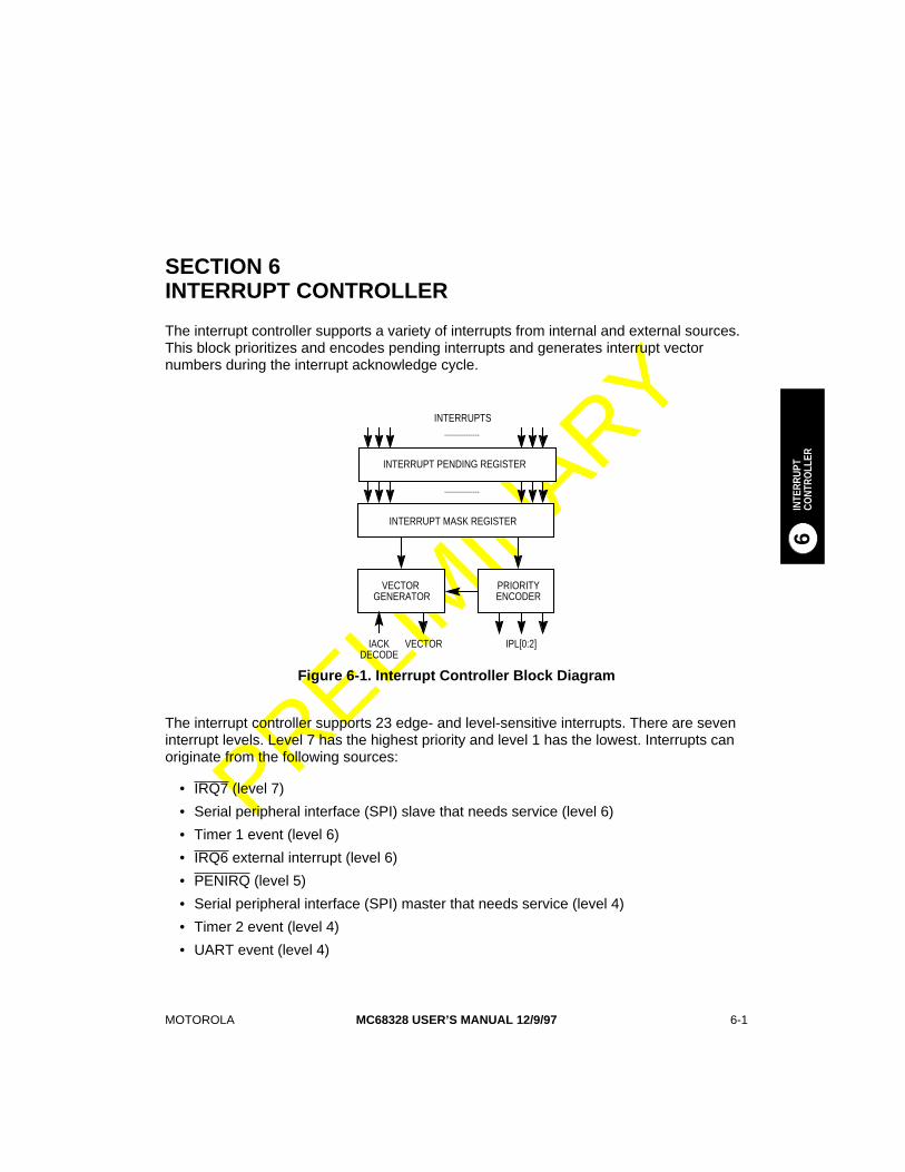
MOTOROLA
MC68328 USER’S MANUAL 12/9/97
6-1
INTE
RRUP
T
6
CONT
ROLL
ER
PRELIM
INARY
SECTION 6INTERRUPT CONTROLLER
The interrupt controller supports a variety of interrupts from internal and external sources. This block prioritizes and encodes pending interrupts and generates interrupt vector numbers during the interrupt acknowledge cycle.
The interrupt controller supports 23 edge- and level-sensitive interrupts. There are seven interrupt levels. Level 7 has the highest priority and level 1 has the lowest. Interrupts can originate from the following sources:
• IRQ7 (level 7)
• Serial peripheral interface (SPI) slave that needs service (level 6)
• Timer 1 event (level 6)
• IRQ6 external interrupt (level 6)
• PENIRQ (level 5)
• Serial peripheral interface (SPI) master that needs service (level 4)
• Timer 2 event (level 4)
• UART event (level 4)
Figure 6-1. Interrupt Controller Block Diagram
................
................
INTERRUPTS
INTERRUPT PENDING REGISTER
INTERRUPT MASK REGISTER
VECTOR PRIORITY
IACK DECODE
VECTOR IPL[0:2]
ENCODERGENERATOR
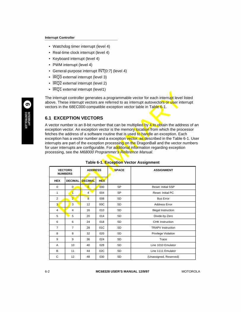
Interrupt Controller
6-2
MC68328 USER’S MANUAL 12/9/97
MOTOROLA
MO
DULEINTERRUPT
6
CONTRO
LLER
PRELIM
INARY
• Watchdog timer interrupt (level 4)
• Real-time clock interrupt (level 4)
• Keyboard interrupt (level 4)
• PWM interrupt (level 4)
• General-purpose interrupt INT[0:7] (level 4)
• IRQ3 external interrupt (level 3)
• IRQ2 external interrupt (level 2)
• IRQ1 external interrupt (level1)
The interrupt controller generates a programmable vector for each interrupt level listed above. These interrupt vectors are referred to as interrupt autovectors or user interrupt vectors in the 68EC000-compatible exception vector table in Table 6-1.
6.1 EXCEPTION VECTORS
A vector number is an 8-bit number that can be multiplied by 4 to obtain the address of an exception vector. An exception vector is the memory location from which the processor fetches the address of a software routine that is used to handle an exception. Each exception has a vector number and a exception vector, as described in the Table 6-1. User interrupts are part of the exception processing on the DragonBall and the vector numbers for user interrupts are configurable. For additional information regarding exception processing, see the
M68000 Programmer’s Reference Manual
.
Table 6-1. Exception Vector Assignment
VECTORS NUMBERS
ADDRESS SPACE ASSIGNMENT
HEX DECIMAL DECIMAL HEX
0 0 0 000 SP Reset: Initial SSP
1 1 4 004 SP Reset: Initial PC
2 2 8 008 SD Bus Error
3 3 12 00C SD Address Error
4 4 16 010 SD Illegal Instruction
5 5 20 014 SD Divide-by-Zero
6 6 24 018 SD CHK Instruction
7 7 28 01C SD TRAPV Instruction
8 8 32 020 SD Privilege Violation
9 9 36 024 SD Trace
A 10 40 028 SD Line 1010 Emulator
B 11 44 02C SD Line 1111 Emulator
C 12 48 030 SD (Unassigned, Reserved)
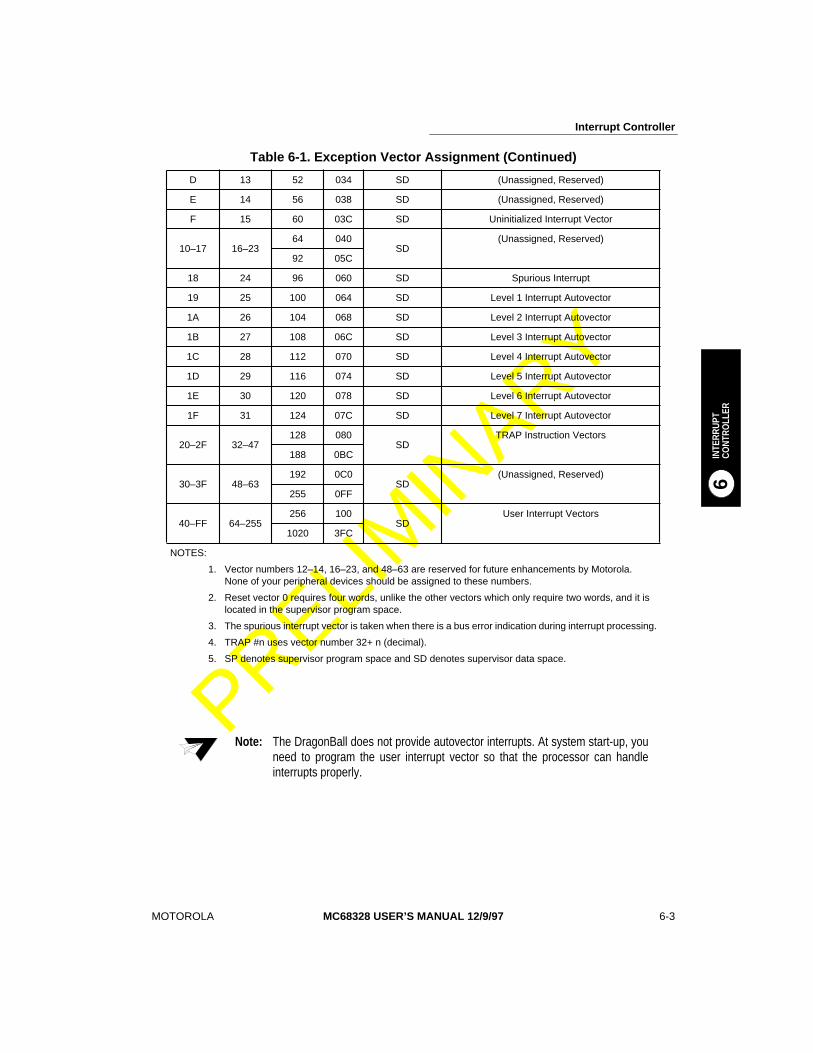
Interrupt Controller
MOTOROLA
MC68328 USER’S MANUAL 12/9/97
6-3
INTE
RRUP
T
6
CONT
ROLL
ER
PRELIM
INARY
D 13 52 034 SD (Unassigned, Reserved)
E 14 56 038 SD (Unassigned, Reserved)
F 15 60 03C SD Uninitialized Interrupt Vector
10–17 16–2364 040
SD(Unassigned, Reserved)
92 05C
18 24 96 060 SD Spurious Interrupt
19 25 100 064 SD Level 1 Interrupt Autovector
1A 26 104 068 SD Level 2 Interrupt Autovector
1B 27 108 06C SD Level 3 Interrupt Autovector
1C 28 112 070 SD Level 4 Interrupt Autovector
1D 29 116 074 SD Level 5 Interrupt Autovector
1E 30 120 078 SD Level 6 Interrupt Autovector
1F 31 124 07C SD Level 7 Interrupt Autovector
20–2F 32–47128 080
SDTRAP Instruction Vectors
188 0BC
30–3F 48–63192 0C0
SD(Unassigned, Reserved)
255 0FF
40–FF 64–255256 100
SDUser Interrupt Vectors
1020 3FC
NOTES:
1. Vector numbers 12–14, 16–23, and 48–63 are reserved for future enhancements by Motorola. None of your peripheral devices should be assigned to these numbers.
2. Reset vector 0 requires four words, unlike the other vectors which only require two words, and it is located in the supervisor program space.
3. The spurious interrupt vector is taken when there is a bus error indication during interrupt processing.
4. TRAP #n uses vector number 32+ n (decimal).
5. SP denotes supervisor program space and SD denotes supervisor data space.
Note:
The DragonBall does not provide autovector interrupts. At system start-up, youneed to program the user interrupt vector so that the processor can handleinterrupts properly.
Table 6-1. Exception Vector Assignment (Continued)
Interrupt Controller
6-4
MC68328 USER’S MANUAL 12/9/97
MOTOROLA
MO
DULEINTERRUPT
6
CONTRO
LLER
PRELIM
INARY
6.2 RESET
The reset exception corresponds to the highest exception level. A reset exception is processed for system initialization and to recover from a catastrophic failure. Any processing that is in progress at the time of the reset is aborted and cannot be recovered. Neither the program counter nor the status register is saved. The processor is forced into the supervisor state. The interrupt priority mask is set at level 7. The address in the first 2 words of the reset exception vector is fetched by the processor as the initial SSP (Supervisor Stack Pointer), and the address in the next two words of the reset exception vector is fetched as the initial program counter.
At start-up or reset, the default chip-select (CSA0) is asserted and all other chip-selects are negated. You should use CSA0 to decode an EPROM/ROM memory space. In this case, the first two long-words of the EPROM/ROM memory space should be programmed to contain the initial SSP and PC. The initial SSP should point to a RAM space and the initial PC should point to the start-up code within the EPROM/ROM space so that the processor can execute the start-up code to bring up the system.
RESET is an input-only pin on the DragonBall. For more information about core interrupts, see the Motorola application note called
A Discussion of Interrupts for the MC68000
(part number AN1012).
6.3 INTERRUPT CONTROLLER
When interrupts are received by the controller, they are prioritized and the highest enabled pending interrupt is posted to the core. Before the CPU responds to this interrupt, the status register is copied internally. Then the S bit of the status register is set, which puts the processor into supervisor mode. The CPU then responds with an interrupt acknowledge cycle, in which the lower 3 bits of the address bus reflect the level of the current interrupt. The interrupt controller generates a vector number during the interrupt acknowledge cycle and the CPU uses this vector number to generate a vector address. Except for the reset exception, the CPU saves the current processor status, including the program counter value (which points to the next instruction to be executed after the interrupt), and the saved copy of the status register. The new program counter is updated to the content of the interrupt vector, which points to the interrupt service routine. The CPU then resumes instruction execution to execute the interrupt service routine.
Interrupt priority is based on the interrupt level. If the CPU is currently processing an interrupt service routine and a higher priority interrupt is posted, the process described above repeats, and the higher priority interrupt is serviced. If the priority of the newer interrupt is lower than or equal to the priority of the current interrupt, execution of the current interrupt handler continues. This newer interrupt is postponed until its priority becomes the highest. Interrupts within a same level should be prioritized in software by the interrupt
Note:
The DragonBall does not support the
reset
instruction. It will not cause a resetexception or an assertion of the RESET pin.
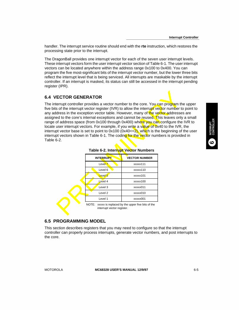
Interrupt Controller
MOTOROLA
MC68328 USER’S MANUAL 12/9/97
6-5
INTE
RRUP
T
6
CONT
ROLL
ER
PRELIM
INARY
handler. The interrupt service routine should end with the
rte
instruction, which restores the processing state prior to the interrupt.
The DragonBall provides one interrupt vector for each of the seven user interrupt levels. These interrupt vectors form the user interrupt vector section of Table 6-1. The user interrupt vectors can be located anywhere within the address range 0x100 to 0x400. You can program the five most-significant bits of the interrupt vector number, but the lower three bits reflect the interrupt level that is being serviced. All interrupts are maskable by the interrupt controller. If an interrupt is masked, its status can still be accessed in the interrupt pending register (IPR).
6.4 VECTOR GENERATOR
The interrupt controller provides a vector number to the core. You can program the upper five bits of the interrupt vector register (IVR) to allow the interrupt vector number to point to any address in the exception vector table. However, many of the vector addresses are assigned to the core’s internal exceptions and cannot be reused. This leaves only a small range of address space (from 0x100 through 0x400) where you can configure the IVR to locate user interrupt vectors. For example, if you write a value of 0x40 to the IVR, the interrupt vector base is set to point to 0x100 (0x40<<2), which is the beginning of the user interrupt vectors shown in Table 6-1. The coding for the vector numbers is provided inTable 6-2.
6.5 PROGRAMMING MODEL
This section describes registers that you may need to configure so that the interrupt controller can properly process interrupts, generate vector numbers, and post interrupts to the core.
Table 6-2. Interrupt Vector Numbers
INTERRUPT VECTOR NUMBER
Level 7 xxxxx111
Level 6 xxxxx110
Level 5 xxxxx101
Level 4 xxxxx100
Level 3 xxxxx011
Level 2 xxxxx010
Level 1 xxxxx001
NOTE: xxxxx is replaced by the upper five bits of the interrupt vector register.
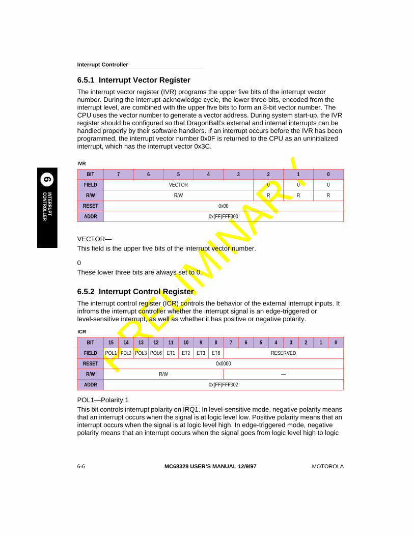
Interrupt Controller
6-6
MC68328 USER’S MANUAL 12/9/97
MOTOROLA
MO
DULEINTERRUPT
6
CONTRO
LLER
PRELIM
INARY
6.5.1 Interrupt Vector Register
The interrupt vector register (IVR) programs the upper five bits of the interrupt vector number. During the interrupt-acknowledge cycle, the lower three bits, encoded from the interrupt level, are combined with the upper five bits to form an 8-bit vector number. The CPU uses the vector number to generate a vector address. During system start-up, the IVR register should be configured so that DragonBall’s external and internal interrupts can be handled properly by their software handlers. If an interrupt occurs before the IVR has been programmed, the interrupt vector number 0x0F is returned to the CPU as an uninitialized interrupt, which has the interrupt vector 0x3C.
VECTOR—This field is the upper five bits of the interrupt vector number.
0These lower three bits are always set to 0.
6.5.2 Interrupt Control Register
The interrupt control register (ICR) controls the behavior of the external interrupt inputs. It infroms the interrupt controller whether the interrupt signal is an edge-triggered or level-sensitive interrupt, as well as whether it has positive or negative polarity.
POL1—Polarity 1This bit controls interrupt polarity on IRQ1. In level-sensitive mode, negative polarity means that an interrupt occurs when the signal is at logic level low. Positive polarity means that an interrupt occurs when the signal is at logic level high. In edge-triggered mode, negative polarity means that an interrupt occurs when the signal goes from logic level high to logic
IVR
BIT 7 6 5 4 3 2 1 0
FIELD
VECTOR 0 0 0
R/W
R/W R R R
RESET
0x00
ADDR
0x(FF)FFF300
ICR
BIT 15 14 13 12 11 10 9 8 7 6 5 4 3 2 1 0
FIELD
POL1
POL2
POL3 POL6 ET1 ET
2
ET3 ET6 RESERVED
RESET
0x0000
R/W
R/W —
ADDR
0x(FF)FFF302
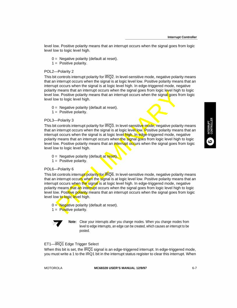
Interrupt Controller
MOTOROLA
MC68328 USER’S MANUAL 12/9/97
6-7
INTE
RRUP
T
6
CONT
ROLL
ER
PRELIM
INARY
level low. Positive polarity means that an interrupt occurs when the signal goes from logic level low to logic level high.
0 = Negative polarity (default at reset).1 = Positive polarity.
POL2—Polarity 2This bit controls interrupt polarity for IRQ2. In level-sensitive mode, negative polarity means that an interrupt occurs when the signal is at logic level low. Positive polarity means that an interrupt occurs when the signal is at logic level high. In edge-triggered mode, negative polarity means that an interrupt occurs when the signal goes from logic level high to logic level low. Positive polarity means that an interrupt occurs when the signal goes from logic level low to logic level high.
0 = Negative polarity (default at reset).1 = Positive polarity.
POL3—Polarity 3This bit controls interrupt polarity for IRQ3. In level-sensitive mode, negative polarity means that an interrupt occurs when the signal is at logic level low. Positive polarity means that an interrupt occurs when the signal is at logic level high. In edge-triggered mode, negative polarity means that an interrupt occurs when the signal goes from logic level high to logic level low. Positive polarity means that an interrupt occurs when the signal goes from logic level low to logic level high.
0 = Negative polarity (default at reset).1 = Positive polarity.
POL6—Polarity 6This bit controls interrupt polarity for IRQ6. In level-sensitive mode, negative polarity means that an interrupt occurs when the signal is at logic level low. Positive polarity means that an interrupt occurs when the signal is at logic level high. In edge-triggered mode, negative polarity means that an interrupt occurs when the signal goes from logic level high to logic level low. Positive polarity means that an interrupt occurs when the signal goes from logic level low to logic level high.
0 = Negative polarity (default at reset).1 = Positive polarity.
ET1—IRQ1 Edge Trigger SelectWhen this bit is set, the IRQ1 signal is an edge-triggered interrupt. In edge-triggered mode, you must write a 1 to the IRQ1 bit in the interrupt status register to clear this interrupt. When
Note:
Clear your interrupts after you change modes. When you change modes fromlevel to edge interrupts, an edge can be created, which causes an interrupt to beposted.
Interrupt Controller
6-8
MC68328 USER’S MANUAL 12/9/97
MOTOROLA
MO
DULEINTERRUPT
6
CONTRO
LLER
PRELIM
INARY
this bit is low, IRQ1 is a level-sensitive interrupt. In this case, you must clear the external source of the interrupt.
0 = Level-sensitive interrupt (default at reset).1 = Edge-sensitive interrupt.
ET2—RQ2 Edge Trigger SelectWhen this bit is set, the IRQ2 signal is an edge-triggered interrupt. In edge-triggered mode, you must write a 1 to the IRQ2 bit in the interrupt status register to clear this interrupt. When this bit is low, IRQ2 is a level-sensitive interrupt. In this case, you must clear the external source of the interrupt.
0 = Level-sensitive interrupt (default at reset).1 = Edge-sensitive interrupt.
ET3—IRQ3 Edge Trigger SelectWhen this bit is set, the IRQ3 signal is an edge-triggered interrupt. In edge-triggered mode, you must write a 1 to the IRQ3 bit in the interrupt status register to clear this interrupt. When this bit is low, IRQ3 is a level-sensitive interrupt. In this case, you must clear the external source of the interrupt.
0 = Level-sensitive interrupt (default at reset).1 = Edge-sensitive interrupt.
ET6—IRQ6 Edge Trigger SelectWhen this bit is set, the IRQ6 signal is an edge-triggered interrupt. In edge-triggered mode, you must write a 1 to the IRQ6 bit in the interrupt status register to clear this interrupt. When this bit is low, IRQ6 is a level-sensitive interrupt. In this case, you must clear the external source of the interrupt.
0 = Level-sensitive interrupt (default at reset).1 = Edge-sensitive interrupt.
Bits 0–7—Reserved These bits are reserved and should remain at their default value.
6.5.3 Interrupt Mask Register
The interrupt mask (IMR) is a control register that can mask out a particular interrupt if the corresponding bit for the interrupt is set. There is one control bit for each interrupt source. When an interrupt is masked, the interrupt controller will not generate an interrupt request
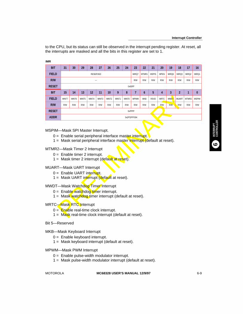
Interrupt Controller
MOTOROLA
MC68328 USER’S MANUAL 12/9/97
6-9
INTE
RRUP
T
6
CONT
ROLL
ER
PRELIM
INARY
to the CPU, but its status can still be observed in the interrupt pending register. At reset, all the interrupts are masked and all the bits in this register are set to 1.
MSPIM—Mask SPI Master Interrupt.0 = Enable serial peripheral interface master interrupt.1 = Mask serial peripheral interface master interrupt (default at reset).
MTMR2—Mask Timer 2 Interrupt0 = Enable timer 2 interrupt.1 = Mask timer 2 interrupt (default at reset).
MUART—Mask UART Interrupt0 = Enable UART interrupt.1 = Mask UART interrupt (default at reset).
MWDT—Mask Watchdog Timer Interrupt0 = Enable watchdog timer interrupt.1 = Mask watchdog timer interrupt (default at reset).
MRTC—Mask RTC Interrupt0 = Enable real-time clock interrupt.1 = Mask real-time clock interrupt (default at reset).
Bit 5—Reserved
MKB—Mask Keyboard Interrupt0 = Enable keyboard interrupt.1 = Mask keyboard interrupt (default at reset).
MPWM—Mask PWM Interrupt0 = Enable pulse-width modulator interrupt.1 = Mask pulse-width modulator interrupt (default at reset).
IMR
BIT 31 30 29 28 27 26 25 24 23 22 21 20 19 18 17 16
FIELD
RESERVED MIRQ7 MTMR1 MSPIS MPEN MIRQ6 MIRQ3 MIRQ2 MIRQ1
R/W
— R/W R/W R/W R/W R/W R/W R/W R/W
RESET
0x00FF
BIT 15 14 13 12 11 10 9 8 7 6 5 4 3 2 1 0
FIELD
MINT7 MINT6 MINT5 MINT4 MINT3 MINT2 MINT1 MINT0 MPWM MKB RSVD MRTC MWDT MUART MTMR2 MSPIM
R/W
R/W R/W R/W R/W R/W R/W R/W R/W R/W R/W R/W R/W R/W R/W R/W R/W
RESET
0xFFFF
ADDR
0x(FF)FFF304
Interrupt Controller
6-10
MC68328 USER’S MANUAL 12/9/97
MOTOROLA
MO
DULEINTERRUPT
6
CONTRO
LLER
PRELIM
INARY
MINT0—Mask External INT0 interrupt0 = Enable INT0 interrupt.1 = Mask INT0 interrupt (default at reset).
MINT1—Mask External INT1 interrupt0 = Enable INT1 interrupt.1 = Mask INT1 interrupt (default at reset).
MINT2—Mask External INT2 interrupt0 = Enable INT2 interrupt.1 = Mask INT2 interrupt (default at reset).
MINT3—Mask External INT3 interrupt0 = Enable INT3 interrupt.1 = Mask INT3 interrupt (default at reset).
MINT4—Mask External INT4 interrupt0 = Enable INT4 interrupt.1 = Mask INT4 interrupt (default at reset).
MINT5—Mask External INT5 interrupt0 = Enable INT5 interrupt.1 = Mask INT5 interrupt (default at reset).
MINT6—Mask External INT6 interrupt0 = Enable INT6 interrupt.1 = Mask INT6 interrupt (default at reset).
MINT7—Mask External INT7 interrupt0 = Enable INT7 interrupt.1 = Mask INT7 interrupt (default at reset).
MIRQ1—Mask IRQ1Interrupt0 = Enable IRQ1 interrupt.1 = Mask IRQ1 interrupt (default at reset).
MIRQ2—Mask IRQ2 Interrupt0 = Enable IRQ2 interrupt.1 = MaskIRQ2 interrupt (default value at reset).
MIRQ3—Mask IRQ3 Interrupt0 = Enable IRQ3 interrupt.1 = Mask IRQ3 interrupt (default value at reset).
Interrupt Controller
MOTOROLA
MC68328 USER’S MANUAL 12/9/97
6-11
INTE
RRUP
T
6
CONT
ROLL
ER
PRELIM
INARY
MIRQ6—Mask IRQ6 Interrupt0 = Enable IRQ6 interrupt.1 = Mask IRQ6 interrupt (default value at reset).
MPEN—Mask Pen Interrupt0 = Enable pen-down interrupt.1 = Mask pen-down interrupt (default value at reset).
MSPIS—Mask Serial Peripheral Interface (SPI) Slave Interrupt0 = Enable SPI slave interrupt.1 = Mask SPI slave interrupt (default value at reset).
MTMR1—Mask Timer 1 Interrupt0 = Enable timer 1 interrupt.1 = Mask timer 1 interrupt (default value at reset).
MIRQ7—Mask IRQ7 InterruptWhen set, this bit indicates that the IRQ7 interrupt is masked. Traditionally, the level 7 interrupt is known as nonmaskable interrupt in the M68000 architecture. This means that when all interrupts are masked in the CPU status register, the level 7 interrupt can still be recognized by the microprocessor. On the MC68328, however, you can set this bit to block IRQ7 interrupt from being sent to the processor.
0 = Enable IRQ7 interrupt.1 = Mask IRQ7 interrupt.
6.5.4 Interrupt Wake-Up Enable Register
The interrupt wake-up enable register (IWR) enables the corresponding interrupt source to start the power-control wake-up sequence. When a bit in this register is set, the corresponding interrupt can cause the processor to wake up from sleep or doze mode. When a bit in this register is cleared, the corresponding interrupt will not be able to wake up the processor. At reset, all bits in this register are set to enable the interrupts to cause a wake-up event. The bit positions in this register correspond to the bits in the interrupt status register, interrupt pending register, and interrupt mask register.
IWR
BIT 31 30 29 28 27 26 25 24 23 22 21 20 19 18 17 16
FIELD
RESERVED IRQ7 TMR1 SPIS PEN IRQ6 IRQ3 IRQ2 IRQ1
BIT 15 14 13 12 11 10 9 8 7 6 5 4 3 2 1 0
FIELD
INT7 INT6 INT5 INT4 INT3 INT2 INT1 INT0 PWM WKB RSVD RTC WDT UART TMR2 SPIM
R/W
R/W R/W R/W R/W R/W R/W R/W R/W R/W R/W R/W R/W R/W R/W R/W R/W
RESET
0xFFFF
ADDR 0x(FF)FFF308
Interrupt Controller
6-12 MC68328 USER’S MANUAL 12/9/97 MOTOROLA
MO
DULEINTERRUPT
6CO
NTROLLER
PRELIM
INARYSPIM—Wake-Up SPI Master Interrupt
0 = Disallow SPI master interrupt from waking up the processor.1 = Enable SPI master interrupt to wake up the processor. (default at reset)
TMR2—Wake-Up Timer 2 Interrupt0 = Disallow timer 2 interrupt from waking up the processor.1 = Enable timer 2 interrupt to wake up the processor (default at reset).
UART—Wake-Up UART Interrupt0 = Disallow UART interrupt from waking up the processor.1 = Enable UART interrupt to wake up the processor (default at reset).
WDT—Wake-up Watchdog Timer Interrupt0 = Disallow watchdog timer interrupt from waking up the processor.1 = Enable watchdog timer interrupt to wake up the processor (default at reset).
RTC—Wake-up RTC Interrupt0 = Disallow real-time clock interrupt from waking up the processor.1 = Enable real-time clock interrupt to wake up the processor (default at reset).
Bit 5—ReservedThese bits are reserved and should remain at their default value.
WKB—Wake-up Keyboard Interrupt0 = Disallow keyboard interrupt from waking up the processor.1 = Enable keyboard interrupt to wake up the processor (default at reset).
PWM—Wake-up PWM Interrupt0 = Disallow pulse-width modulator interrupt from waking up the processor.1 = Enable pulse-width modulator interrupt to wake up the processor (default at reset).
R/W — R/W R/W R/W R/W R/W R/W R/W R/W
RESET 0x00FF
IWR
BIT 31 30 29 28 27 26 25 24 23 22 21 20 19 18 17 16
BIT 15 14 13 12 11 10 9 8 7 6 5 4 3 2 1 0
FIELD INT7 INT6 INT5 INT4 INT3 INT2 INT1 INT0 PWM WKB RSVD RTC WDT UART TMR2 SPIM
R/W R/W R/W R/W R/W R/W R/W R/W R/W R/W R/W R/W R/W R/W R/W R/W R/W
RESET 0xFFFF
ADDR 0x(FF)FFF308
Interrupt Controller
MOTOROLA MC68328 USER’S MANUAL 12/9/97 6-13
INTE
RRUP
T6
CONT
ROLL
ERPRELI
MIN
ARY
INT0—Wake-up External INT00 = Disallow INT0 interrupt from waking up the processor.1 = Enable INT0 interrupt to wake up the processor (default at reset).
INT1—Wake-up External INT10 = Disallow INT1 interrupt from waking up the processor.1 = Enable INT1 interrupt to wake up the processor (default at reset).
INT2—Wake-up External INT20 = Disallow INT2 interrupt from waking up the processor.1 = Enable INT2 interrupt to wake up the processor (default at reset).
INT3—Wake-up External INT30 = Disallow INT3 interrupt from waking up the processor.1 = Enable INT3 interrupt to wake up the processor (default at reset).
INT4—Wake-up External INT40 = Disallow INT4 interrupt from waking up the processor.1 = Enable INT4 interrupt to wake up the processor (default at reset).
INT5—Wake-up External INT50 = Disallow INT5 interrupt to wake up the processor.1 = Enable INT5 interrupt to wake up the processor (default at reset).
INT6—Wake-up External INT60 = Disallow INT6 interrupt from waking up the processor.1 = Enable INT6 interrupt to wake up the processor (default at reset).
INT7—Wake-up External INT70 = Disallow INT7 interrupt from waking up the processor.1 = Enable INT7 interrupt to wake up the processor (default at reset).
IRQ1—Wake-up IRQ1Interrupt0 = Disallow IRQ1 interrupt from waking up the processor.1 = Enable IRQ1interrupt to wake up the processor (default at reset).
IRQ2—Wake-up IRQ2 Interrupt0 = Disallow IRQ2 interrupt from waking up the processor.1 = Enable IRQ2 interrupt to wake up the processor (default at reset).
IRQ3—Wake-up IRQ3 Interrupt0 = Disallow IRQ3 interrupt from waking up the processor.1 = Enable IRQ3 interrupt to wake up the processor (default at reset).
Interrupt Controller
6-14 MC68328 USER’S MANUAL 12/9/97 MOTOROLA
MO
DULEINTERRUPT
6CO
NTROLLER
PRELIM
INARY
IRQ6—Wake-up IRQ6 Interrupt0 = Disallow IRQ6 interrupt from waking up the processor.1 = Enable IRQ6 interrupt to wake up the processor (default at reset).
PEN—Wake-up Pen Interrupt0 = Disallow pen-down interrupt from waking up the processor.1 = Enable pen-down interrupt to wake up the processor (default at reset).
SPIS—Wake-up Serial Peripheral Interface (SPI) Slave Interrupt0 = Disallow SPI slave interrupt from waking up the processor.1 = Enable SPI slave interrupt to wake up the processor (default at reset).
TMR1—Wake-up Timer 1 Interrupt0 = Disallow timer 1 interrupt from waking up the processor.1 = Enable timer 1 interrupt to wake up the processor (default at reset).
IRQ7—Wake-up IRQ7 Interrupt0 = Disallow IRQ7 interrupt from waking up the processor.1 = Enable IRQ7 interrupt to wake up the processor (default at reset).
6.5.5 Interrupt Status RegisterDuring the interrupt service, the interrupt handler can determine the source of the interrupt by examining the interrupt status register (ISR). Each bit in this register, when set, indicates the corresponding interrupt is posted to the core. If there are multiple interrupt sources at the same level, the software handler may need to prioritize them, depending on the application.
Each interrupt status bit in the interrupt status register reflects the interrupt request from their respective interrupt sources. Refer to the specific sections about the timer, SPI master, SPI slave, real-time clock, and pulse-width modulation for details about how to clear the interrupt. The IRQ7 signal is an active-low edge-triggered interrupt request and an IRQ7 interrupt is clear by writing a 1 to the IRQ7 status bit. When programmed as edge-triggered interrupts, IRQ1, IRQ2, IRQ3, and IRQ6 interrupts can be cleared by writing a 1 to the corresponding status bit in the register. When programmed as level-triggered interrupts, these interrupts are cleared at the requesting sources.
SPIM—SPI Master Interrupt RequestWhen this bit is set, it indicates that a data transfer is complete. You must clear this interrupt in the serial peripheral interface control register. This interrupt is a level 4 interrupt.
0 = No SPI Master interrupt pending.1 = A SPI Master interrupt is posted.
Interrupt Controller
MOTOROLA MC68328 USER’S MANUAL 12/9/97 6-15
INTE
RRUP
T6
CONT
ROLL
ERPRELI
MIN
ARY
TIMER2—Timer 2 Interrupt RequestThis bit indicates that a timer 2 event has occurred. This is a level 4 interrupt. See Section 8 Timers for more information about timer operation.
0 = No timer 2 event occurred.1 = Timer 2 event has occurred.
UART—UART Interrupt RequestWhen this bit is set, it indicates that the UART module needs service. This is a level 4 interrupt.
0 = No UART service request is pending.1 = UART service is needed.
WDT—Watchdog Timer Interrupt RequestThis bit indicates that a watchdog timer interrupt is pending.
0 = No watchdog timer interrupt1 = A watchdog timer interrupt is pending
RTC—Real-Time Clock Interrupt RequestThis bit indicates that the real-time clock is requesting an interrupt.
0 = No real-time clock interrupt1 = A real-time clock interrupt is pending
Bit 5—ReservedThis bit is reserved and should remain at its default value.
KB—Keyboard Interrupt RequestThis bit indicates whether there is a keyboard interrupt.
0 = No keyboard interrupt.1 = Keyboard interrupt is pending.
PWM—Pulse-Width Modulator InterruptThis bit indicates that a PWM period rollover event occurs. This is a level 4 interrupt.
0 = No pulse-width modulator period rollover event occurred.1 = Pulse-width modulator period rolled over.
INT0—External INT0 Interrupt0 = No INT0 interrupt.1 = INT0 interrupt is pending.
INT1—External INT1 Interrupt0 = No INT1 interrupt.1 = INT1 interrrupt is pending.
Interrupt Controller
6-16 MC68328 USER’S MANUAL 12/9/97 MOTOROLA
MO
DULEINTERRUPT
6CO
NTROLLER
PRELIM
INARY
INT2—External INT2 Interrupt0 = No INT2 interrupt.1 = INT2 interrupt is pending.
INT3—External INT3 Interrupt0 = No INT3 interrupt.1 = INT3 interrupt is pending.
INT4—External INT4 Interrupt0 = No INT4 interrupt.1 = INT4 interrupt is pending.
INT5—External INT5 Interrupt0 = No INT5 interrupt.1 = INT5 interrupt is pending.
INT6— External INT6 Interrupt0 = No INT6 interrupt.1 = INT6 interrupt is pending.
INT7— External INT7 Interrupt0 = No INT7 interrupt.1 = INT7 interrupt is pending.
IRQ1—Interrupt Request Level 1When set, this bit indicates that an external device has requested an interrupt on level 1. If IRQ1 signal is set to be a level-sensitive interrupt, you must clear the source of the interrupt. If IRQ1 signal is set to be an edge-triggered interrupt, you must clear the interrupt by writing a 1 to this bit (writing a 0 has no effect).
0 = No level 1 interrupt is pending.1 = Level 1 interrupt is pending.
IRQ2—Interrupt Request Level 2When set, this bit indicates that an external device has requested an interrupt on level 2. If IRQ2 signal is set to be a level-sensitive interrupt, you must clear the source of the interrupt. If IRQ2 signal is set to be an edge-triggered interrupt, you must clear the interrupt by writing a 1 to this bit (writing a 0 has no effect).
0 = No level 2 interrupt is pending.1 = Level 2 interrupt is pending.
IRQ3—Interrupt Request Level 3When set, this bit indicates that an external device has requested an interrupt on level 3. If IRQ3 signal is set to be a level-sensitive interrupt, you must clear the source of the interrupt.
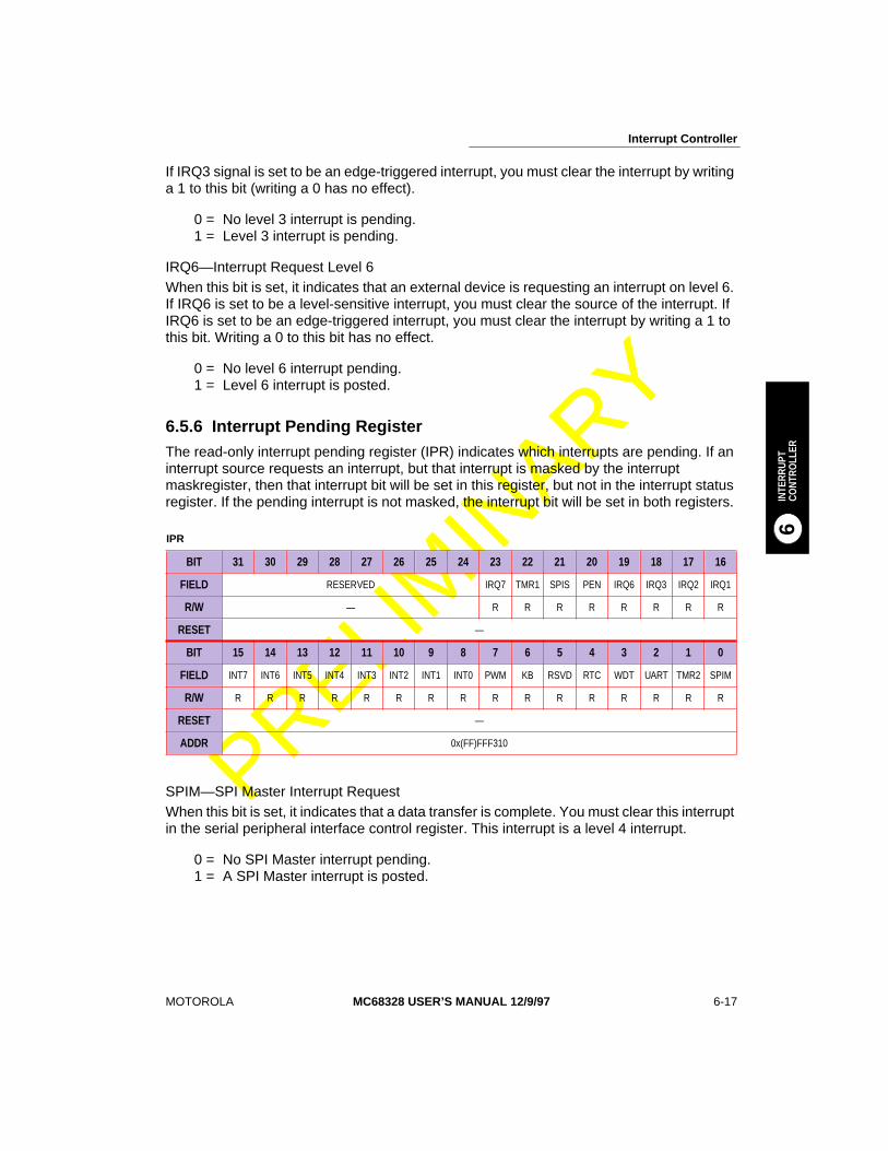
Interrupt Controller
MOTOROLA MC68328 USER’S MANUAL 12/9/97 6-17
INTE
RRUP
T6
CONT
ROLL
ERPRELI
MIN
ARY
If IRQ3 signal is set to be an edge-triggered interrupt, you must clear the interrupt by writing a 1 to this bit (writing a 0 has no effect).
0 = No level 3 interrupt is pending.1 = Level 3 interrupt is pending.
IRQ6—Interrupt Request Level 6When this bit is set, it indicates that an external device is requesting an interrupt on level 6. If IRQ6 is set to be a level-sensitive interrupt, you must clear the source of the interrupt. If IRQ6 is set to be an edge-triggered interrupt, you must clear the interrupt by writing a 1 to this bit. Writing a 0 to this bit has no effect.
0 = No level 6 interrupt pending.1 = Level 6 interrupt is posted.
6.5.6 Interrupt Pending RegisterThe read-only interrupt pending register (IPR) indicates which interrupts are pending. If an interrupt source requests an interrupt, but that interrupt is masked by the interrupt maskregister, then that interrupt bit will be set in this register, but not in the interrupt status register. If the pending interrupt is not masked, the interrupt bit will be set in both registers.
SPIM—SPI Master Interrupt RequestWhen this bit is set, it indicates that a data transfer is complete. You must clear this interrupt in the serial peripheral interface control register. This interrupt is a level 4 interrupt.
0 = No SPI Master interrupt pending.1 = A SPI Master interrupt is posted.
IPR
BIT 31 30 29 28 27 26 25 24 23 22 21 20 19 18 17 16
FIELD RESERVED IRQ7 TMR1 SPIS PEN IRQ6 IRQ3 IRQ2 IRQ1
R/W — R R R R R R R R
RESET —
BIT 15 14 13 12 11 10 9 8 7 6 5 4 3 2 1 0
FIELD INT7 INT6 INT5 INT4 INT3 INT2 INT1 INT0 PWM KB RSVD RTC WDT UART TMR2 SPIM
R/W R R R R R R R R R R R R R R R R
RESET —
ADDR 0x(FF)FFF310
Interrupt Controller
6-18 MC68328 USER’S MANUAL 12/9/97 MOTOROLA
MO
DULEINTERRUPT
6CO
NTROLLER
PRELIM
INARY
TIMER2—Timer 2 Interrupt RequestThis bit indicates that a timer 2 event has occurred. This is a level 4 interrupt. See Section 8 Timers for more information about timer operation.
0 = No timer 2 event occurred.1 = Timer 2 event has occurred.
UART—UART Interrupt RequestWhen this bit is set, it indicates that the UART module needs service. This is a level 4 interrupt.
0 = No UART service request is pending.1 = UART service is needed.
WDT—Watchdog Timer Interrupt RequestThis bit indicates that a watchdog timer interrupt is pending.
0 = No watchdog timer interrupt1 = A watchdog timer interrupt is pending
RTC—Real-Time Clock Interrupt RequestThis bit indicates that the real-time clock is requesting an interrupt.
0 = No real-time clock interrupt1 = A real-time clock interrupt is pending
Bit 5—ReservedThis bit is reserved and should remain at its default value.
KB—Keyboard Interrupt RequestThis bit indicates whether there is a keyboard interrupt.
0 = No keyboard interrupt.1 = Keyboard interrupt is pending.
PWM—Pulse-Width Modulator InterruptThis bit indicates that a PWM period rollover event occurs. This is a level 4 interrupt.
0 = No pulse-width modulator period rollover event occurred.1 = Pulse-width modulator period rolled over.
INT0—External INT0 Interrupt0 = No INT0 interrupt.1 = INT0 interrupt is pending.
INT1—External INT1 Interrupt0 = No INT1 interrupt.1 = INT1 interrrupt is pending.
Interrupt Controller
MOTOROLA MC68328 USER’S MANUAL 12/9/97 6-19
INTE
RRUP
T6
CONT
ROLL
ERPRELI
MIN
ARY
INT2—External INT2 Interrupt0 = No INT2 interrupt.1 = INT2 interrupt is pending.
INT3—External INT3 Interrupt0 = No INT3 interrupt.1 = INT3 interrupt is pending.
INT4—External INT4 Interrupt0 = No INT4 interrupt.1 = INT4 interrupt is pending.
INT5—External INT5 Interrupt0 = No INT5 interrupt.1 = INT5 interrupt is pending.
INT6— External INT6 Interrupt0 = No INT6 interrupt.1 = INT6 interrupt is pending.
INT7— External INT7 Interrupt0 = No INT7 interrupt.1 = INT7 interrupt is pending.
IRQ1—Interrupt Request Level 1When set, this bit indicates that an external device has requested an interrupt on level 1. If IRQ1 signal is set to be a level-sensitive interrupt, you must clear the source of the interrupt. If IRQ1 signal is set to be an edge-triggered interrupt, you must clear the interrupt by writing a 1 to this bit (writing a 0 has no effect).
0 = No level 1 interrupt is pending.1 = Level 1 interrupt is pending.
IRQ2—Interrupt Request Level 2When set, this bit indicates that an external device has requested an interrupt on level 2. If IRQ2 signal is set to be a level-sensitive interrupt, you must clear the source of the interrupt. If IRQ2 signal is set to be an edge-triggered interrupt, you must clear the interrupt by writing a 1 to this bit (writing a 0 has no effect).
0 = No level 2 interrupt is pending.1 = Level 2 interrupt is pending.
IRQ3—Interrupt Request Level 3When set, this bit indicates that an external device has requested an interrupt on level 3. If IRQ3 signal is set to be a level-sensitive interrupt, you must clear the source of the interrupt.
Interrupt Controller
6-20 MC68328 USER’S MANUAL 12/9/97 MOTOROLA
MO
DULEINTERRUPT
6CO
NTROLLER
PRELIM
INARY
If IRQ3 signal is set to be an edge-triggered interrupt, you must clear the interrupt by writing a 1 to this bit (writing a 0 has no effect).
0 = No level 3 interrupt is pending.1 = Level 3 interrupt is pending.
IRQ6—Interrupt Request Level 6When this bit is set, it indicates that an external device is requesting an interrupt on level 6. If IRQ6 is set to be a level-sensitive interrupt, you must clear the source of the interrupt. If IRQ6 is set to be an edge-triggered interrupt, you must clear the interrupt by writing a 1 to this bit. Writing a 0 to this bit has no effect.
0 = No level 6 interrupt pending.1 = Level 6 interrupt is posted.
MOTOROLA
MC68328 USER’S MANUAL 12/9/97
7-1
PARA
LLEL
PO
RTS
7
PRELIM
INARY
SECTION 7PARALLEL PORTS
The DragonBall microprocessor supports up to 10 parallel ports, that can be configured either as general-purpose input/output ports or as a dedicated peripheral interface. There are three types of ports—basic, pull-up, and interrupt. This section describes these ports and how to configure their functions.
7.1 BASIC PORTS
The basic ports (A, B, C, E, F, G, J, and K) multiplex two functions on each port pin:
• A general I/O function
• A special-purpose function to support on-chip modules
Each port has three configurable 8-bit registers—a data register, direction register, and select register. Each of the 8 bits in the registers affect the function, direction, and output data of each of the corresponding eight pins of a given port. For example, you can configure each bit in the select register of a particular port to choose the associated pin’s function.
The direction register determines whether a port pin is an output or input pin. If you configure the SEL bit for a particular pin to be used with a special-purpose function, then the direction of the pin will depend on that function. In this case, configuring the corresponding bit in the direction register does not have any effect on the pin. The corresponding bit in the data register reflects the current logic level on the pin. If you configure the SEL bit for a particular pin to be used with a general I/O function, then you may have to choose whether this pin will be used as an input or output. If the port pin is used as an input pin, the corresponding bit in the data register reflects the current logic level on the pin. If the port pin is used as an output pin, setting the corresponding bit in the data register will output a “1”, and clearing the bit will produce a “0” output.
If the SEL bit for a particular pin is cleared, you configure the port pin to have a special-purpose function. For example, while the port K Bit 0 of the select register is cleared, this pin is the output master serial peripheral interface TXD signal. In this case,
Data to Module
signal in Figure 7-1 is connected to the master serial peripheral interface TXD signal. Since this bit is output-only, the
Output Enable from module
signal is always asserted and the
Data to module
signal is not used. Another example is that the port K Bit 1 can be used as the master serial peripheral interface RXD input-only signal. In this case, the
Output Enable from module
input is negated and the
Data from module
signal is not used. The
Data to module
signal is connected to the master serial peripheral interface RXD input.
Figure 7-1 illustrates the internal logic of each basic port.
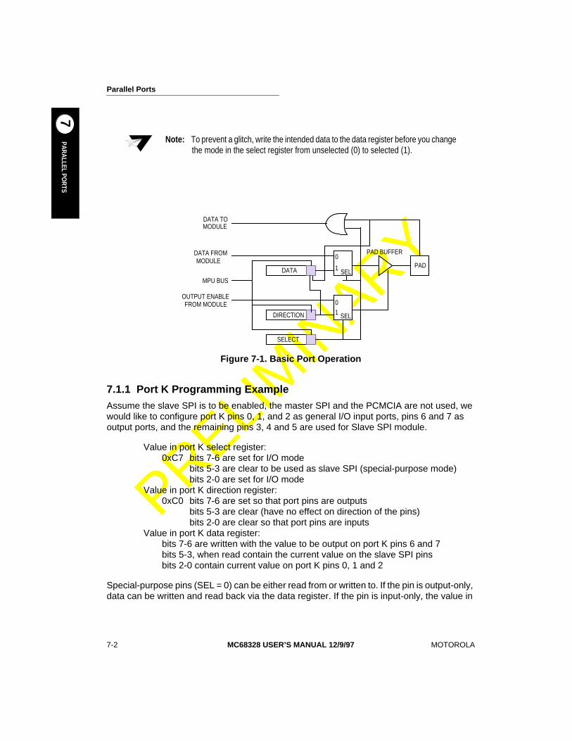
Parallel Ports
7-2
MC68328 USER’S MANUAL 12/9/97
MOTOROLA
PARALLEL PORTS
7
PRELIM
INARY
7.1.1 Port K Programming Example
Assume the slave SPI is to be enabled, the master SPI and the PCMCIA are not used, we would like to configure port K pins 0, 1, and 2 as general I/O input ports, pins 6 and 7 as output ports, and the remaining pins 3, 4 and 5 are used for Slave SPI module.
Value in port K select register:0xC7 bits 7-6 are set for I/O mode
bits 5-3 are clear to be used as slave SPI (special-purpose mode)bits 2-0 are set for I/O mode
Value in port K direction register:0xC0 bits 7-6 are set so that port pins are outputs
bits 5-3 are clear (have no effect on direction of the pins)bits 2-0 are clear so that port pins are inputs
Value in port K data register:bits 7-6 are written with the value to be output on port K pins 6 and 7bits 5-3, when read contain the current value on the slave SPI pinsbits 2-0 contain current value on port K pins 0, 1 and 2
Special-purpose pins (SEL = 0) can be either read from or written to. If the pin is output-only, data can be written and read back via the data register. If the pin is input-only, the value in
Note:
To prevent a glitch, write the intended data to the data register before you changethe mode in the select register from unselected (0) to selected (1).
Figure 7-1. Basic Port Operation
0
1 SEL
01 SEL
SELECT
DIRECTION
DATA
PAD BUFFER
DATA TOMODULE
DATA FROMMODULE
OUTPUT ENABLEFROM MODULE
MPU BUS
PAD
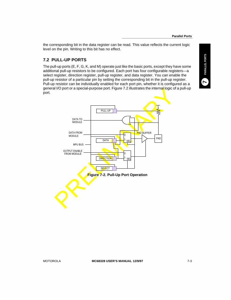
Parallel Ports
MOTOROLA
MC68328 USER’S MANUAL 12/9/97
7-3
PARA
LLEL
PO
RTS
7
PRELIM
INARY
the corresponding bit in the data register can be read. This value reflects the current logic level on the pin. Writing to this bit has no effect.
7.2 PULL-UP PORTS
The pull-up ports (E, F, G, K, and M) operate just like the basic ports, except they have some additional pull-up resistors to be configured. Each port has four configurable registers—a select register, direction register, pull-up register, and data register. You can enable the pull-up resistor of a particular pin by setting the corresponding bit in the pull-up register. Pull-up resistor can be individually enabled for each port pin, whether it is configured as a general I/O port or a special-purpose port. Figure 7.2 illustrates the internal logic of a pull-up port.
Figure 7-2. Pull-Up Port Operation
0
1 SEL
01 SEL
SELECT
DIRECTION
DATA
PAD BUFFER
PAD
DATA TOMODULE
DATA FROMMODULE
OUTPUT ENABLEFROM MODULE
MPU BUS
PULL-UP
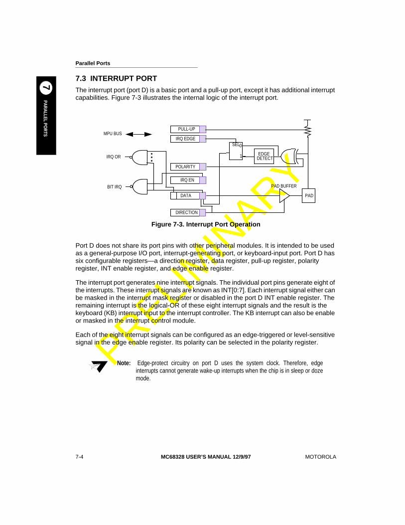
Parallel Ports
7-4
MC68328 USER’S MANUAL 12/9/97
MOTOROLA
PARALLEL PORTS
7
PRELIM
INARY
7.3 INTERRUPT PORT
The interrupt port (port D) is a basic port and a pull-up port, except it has additional interrupt capabilities. Figure 7-3 illustrates the internal logic of the interrupt port.
Port D does not share its port pins with other peripheral modules. It is intended to be used as a general-purpose I/O port, interrupt-generating port, or keyboard-input port. Port D has six configurable registers—a direction register, data register, pull-up register, polarity register, INT enable register, and edge enable register.
The interrupt port generates nine interrupt signals. The individual port pins generate eight of the interrupts. These interrupt signals are known as INT[0:7]. Each interrupt signal either can be masked in the interrupt mask register or disabled in the port D INT enable register. The remaining interrupt is the logical-OR of these eight interrupt signals and the result is the keyboard (KB) interrupt input to the interrupt controller. The KB interrupt can also be enable or masked in the interrupt control module.
Each of the eight interrupt signals can be configured as an edge-triggered or level-sensitive signal in the edge enable register. Its polarity can be selected in the polarity register.
Figure 7-3. Interrupt Port Operation
Note:
Edge-protect circuitry on port D uses the system clock. Therefore, edgeinterrupts cannot generate wake-up interrupts when the chip is in sleep or dozemode.
PAD BUFFER
PAD
PULL-UP
DIRECTION
IRQ EN
DATA
POLARITY
IRQ EDGE0
1
SEL
EDGEDETECTIRQ OR
BIT IRQ
MPU BUS
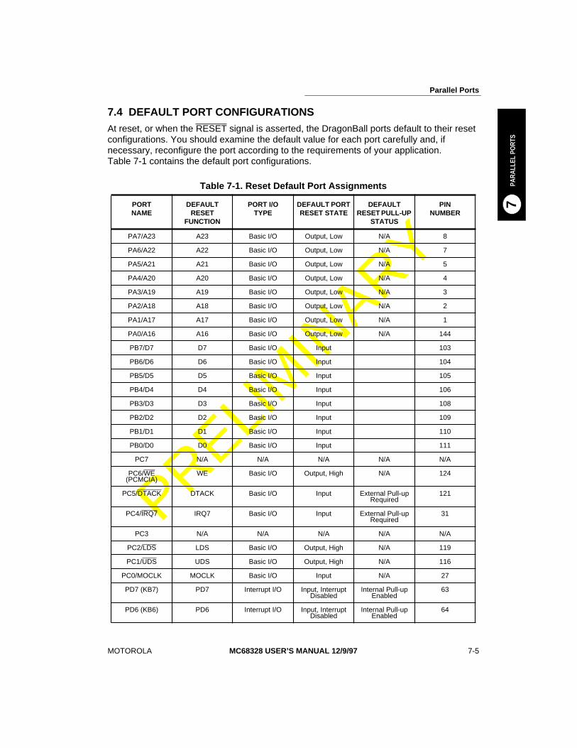
Parallel Ports
MOTOROLA
MC68328 USER’S MANUAL 12/9/97
7-5
PARA
LLEL
PO
RTS
7
PRELIM
INARY
7.4 DEFAULT PORT CONFIGURATIONS
At reset, or when the RESET signal is asserted, the DragonBall ports default to their reset configurations. You should examine the default value for each port carefully and, if necessary, reconfigure the port according to the requirements of your application. Table 7-1 contains the default port configurations.
Table 7-1. Reset Default Port Assignments
PORT NAME
DEFAULT RESET
FUNCTION
PORT I/O TYPE
DEFAULT PORT RESET STATE
DEFAULT RESET PULL-UP
STATUS
PIN NUMBER
PA7/A23 A23 Basic I/O Output, Low N/A 8
PA6/A22 A22 Basic I/O Output, Low N/A 7
PA5/A21 A21 Basic I/O Output, Low N/A 5
PA4/A20 A20 Basic I/O Output, Low N/A 4
PA3/A19 A19 Basic I/O Output, Low N/A 3
PA2/A18 A18 Basic I/O Output, Low N/A 2
PA1/A17 A17 Basic I/O Output, Low N/A 1
PA0/A16 A16 Basic I/O Output, Low N/A 144
PB7/D7 D7 Basic I/O Input 103
PB6/D6 D6 Basic I/O Input 104
PB5/D5 D5 Basic I/O Input 105
PB4/D4 D4 Basic I/O Input 106
PB3/D3 D3 Basic I/O Input 108
PB2/D2 D2 Basic I/O Input 109
PB1/D1 D1 Basic I/O Input 110
PB0/D0 D0 Basic I/O Input 111
PC7 N/A N/A N/A N/A N/A
PC6/WE (PCMCIA)
WE Basic I/O Output, High N/A 124
PC5/DTACK DTACK Basic I/O Input External Pull-up Required
121
PC4/IRQ7 IRQ7 Basic I/O Input External Pull-up Required
31
PC3 N/A N/A N/A N/A N/A
PC2/LDS LDS Basic I/O Output, High N/A 119
PC1/UDS UDS Basic I/O Output, High N/A 116
PC0/MOCLK MOCLK Basic I/O Input N/A 27
PD7 (KB7) PD7 Interrupt I/O Input, Interrupt Disabled
Internal Pull-up Enabled
63
PD6 (KB6) PD6 Interrupt I/O Input, Interrupt Disabled
Internal Pull-up Enabled
64
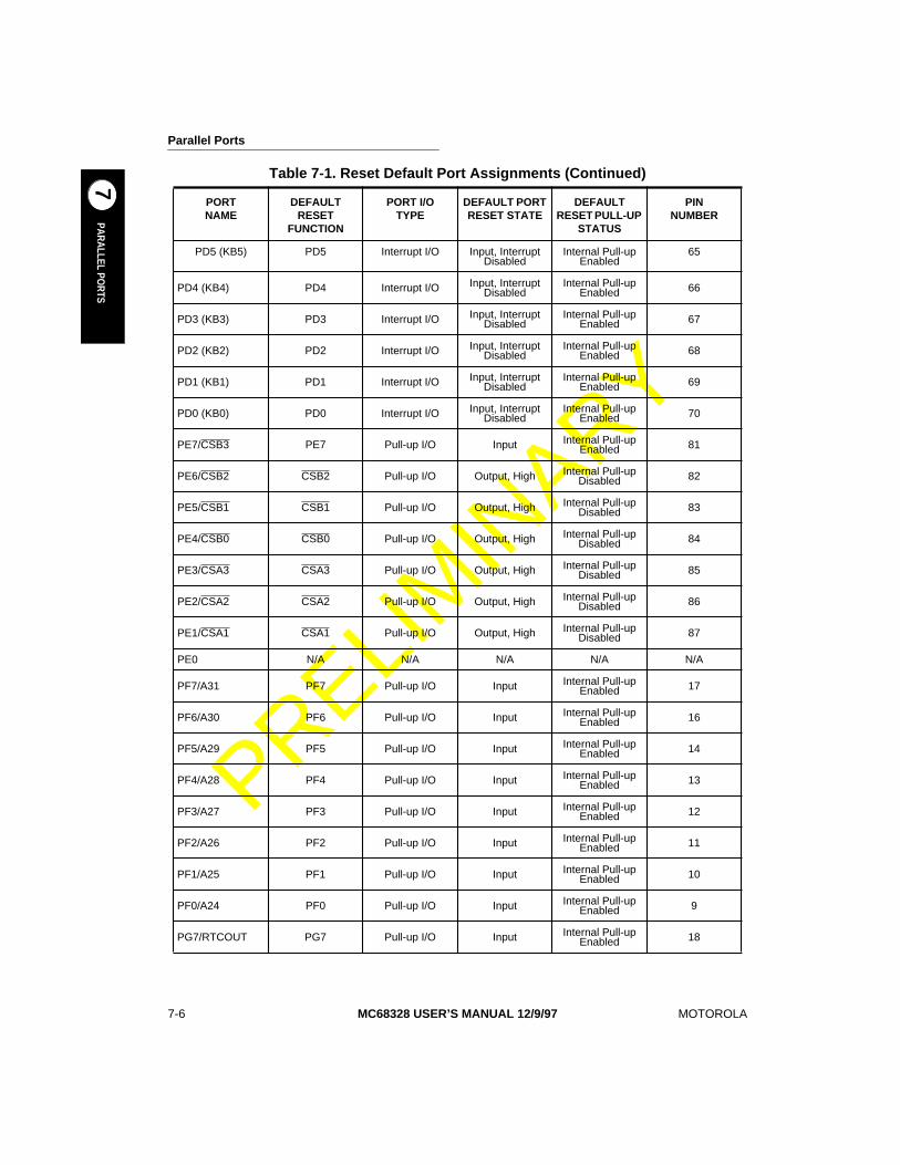
Parallel Ports
7-6
MC68328 USER’S MANUAL 12/9/97
MOTOROLA
PARALLEL PORTS
7
PRELIM
INARY
PD5 (KB5) PD5 Interrupt I/O Input, Interrupt Disabled
Internal Pull-up Enabled
65
PD4 (KB4) PD4 Interrupt I/O Input, Interrupt Disabled
Internal Pull-up Enabled 66
PD3 (KB3) PD3 Interrupt I/O Input, Interrupt Disabled
Internal Pull-up Enabled 67
PD2 (KB2) PD2 Interrupt I/O Input, Interrupt Disabled
Internal Pull-up Enabled 68
PD1 (KB1) PD1 Interrupt I/O Input, Interrupt Disabled
Internal Pull-up Enabled 69
PD0 (KB0) PD0 Interrupt I/O Input, Interrupt Disabled
Internal Pull-up Enabled 70
PE7/CSB3 PE7 Pull-up I/O Input Internal Pull-up Enabled 81
PE6/CSB2 CSB2 Pull-up I/O Output, High Internal Pull-up Disabled 82
PE5/CSB1 CSB1 Pull-up I/O Output, High Internal Pull-up Disabled 83
PE4/CSB0 CSB0 Pull-up I/O Output, High Internal Pull-up Disabled 84
PE3/CSA3 CSA3 Pull-up I/O Output, High Internal Pull-up Disabled 85
PE2/CSA2 CSA2 Pull-up I/O Output, High Internal Pull-up Disabled 86
PE1/CSA1 CSA1 Pull-up I/O Output, High Internal Pull-up Disabled 87
PE0 N/A N/A N/A N/A N/A
PF7/A31 PF7 Pull-up I/O Input Internal Pull-up Enabled 17
PF6/A30 PF6 Pull-up I/O Input Internal Pull-up Enabled 16
PF5/A29 PF5 Pull-up I/O Input Internal Pull-up Enabled 14
PF4/A28 PF4 Pull-up I/O Input Internal Pull-up Enabled 13
PF3/A27 PF3 Pull-up I/O Input Internal Pull-up Enabled 12
PF2/A26 PF2 Pull-up I/O Input Internal Pull-up Enabled 11
PF1/A25 PF1 Pull-up I/O Input Internal Pull-up Enabled 10
PF0/A24 PF0 Pull-up I/O Input Internal Pull-up Enabled 9
PG7/RTCOUT PG7 Pull-up I/O Input Internal Pull-up Enabled 18
Table 7-1. Reset Default Port Assignments (Continued)
PORT NAME
DEFAULT RESET
FUNCTION
PORT I/O TYPE
DEFAULT PORT RESET STATE
DEFAULT RESET PULL-UP
STATUS
PIN NUMBER
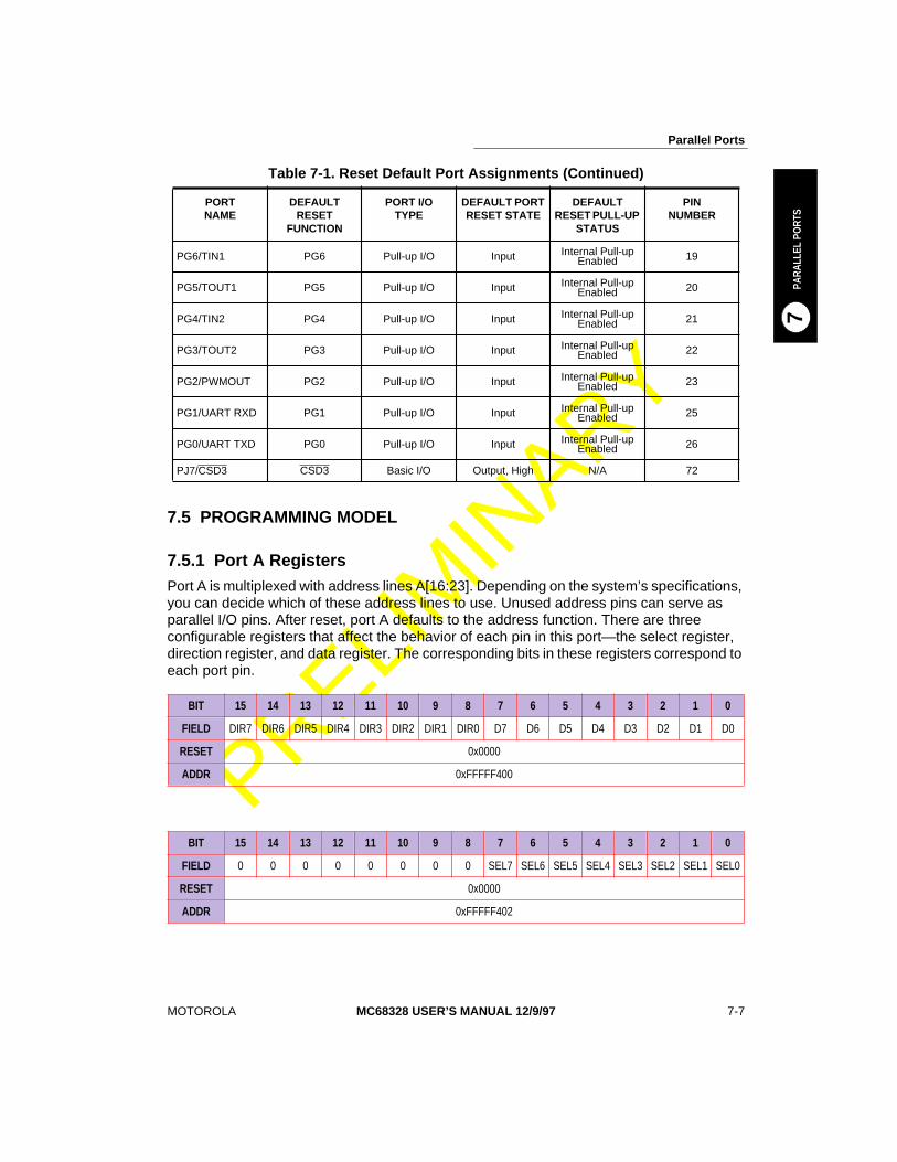
Parallel Ports
MOTOROLA
MC68328 USER’S MANUAL 12/9/97
7-7
PARA
LLEL
PO
RTS
7
PRELIM
INARY
7.5 PROGRAMMING MODEL
7.5.1 Port A Registers
Port A is multiplexed with address lines A[16:23]. Depending on the system’s specifications, you can decide which of these address lines to use. Unused address pins can serve as parallel I/O pins. After reset, port A defaults to the address function. There are three configurable registers that affect the behavior of each pin in this port—the select register, direction register, and data register. The corresponding bits in these registers correspond to each port pin.
PG6/TIN1 PG6 Pull-up I/O Input Internal Pull-up Enabled 19
PG5/TOUT1 PG5 Pull-up I/O Input Internal Pull-up Enabled 20
PG4/TIN2 PG4 Pull-up I/O Input Internal Pull-up Enabled 21
PG3/TOUT2 PG3 Pull-up I/O Input Internal Pull-up Enabled 22
PG2/PWMOUT PG2 Pull-up I/O Input Internal Pull-up Enabled 23
PG1/UART RXD PG1 Pull-up I/O Input Internal Pull-up Enabled 25
PG0/UART TXD PG0 Pull-up I/O Input Internal Pull-up Enabled 26
PJ7/CSD3 CSD3 Basic I/O Output, High N/A 72
BIT 15 14 13 12 11 10 9 8 7 6 5 4 3 2 1 0
FIELD
DIR7 DIR6 DIR5 DIR4 DIR3 DIR2 DIR1 DIR0 D7 D6 D5 D4 D3 D2 D1 D0
RESET
0x0000
ADDR
0xFFFFF400
BIT 15 14 13 12 11 10 9 8 7 6 5 4 3 2 1 0
FIELD
0 0 0 0 0 0 0 0 SEL7 SEL6 SEL5 SEL4 SEL3 SEL2 SEL1 SEL0
RESET
0x0000
ADDR
0xFFFFF402
Table 7-1. Reset Default Port Assignments (Continued)
PORT NAME
DEFAULT RESET
FUNCTION
PORT I/O TYPE
DEFAULT PORT RESET STATE
DEFAULT RESET PULL-UP
STATUS
PIN NUMBER
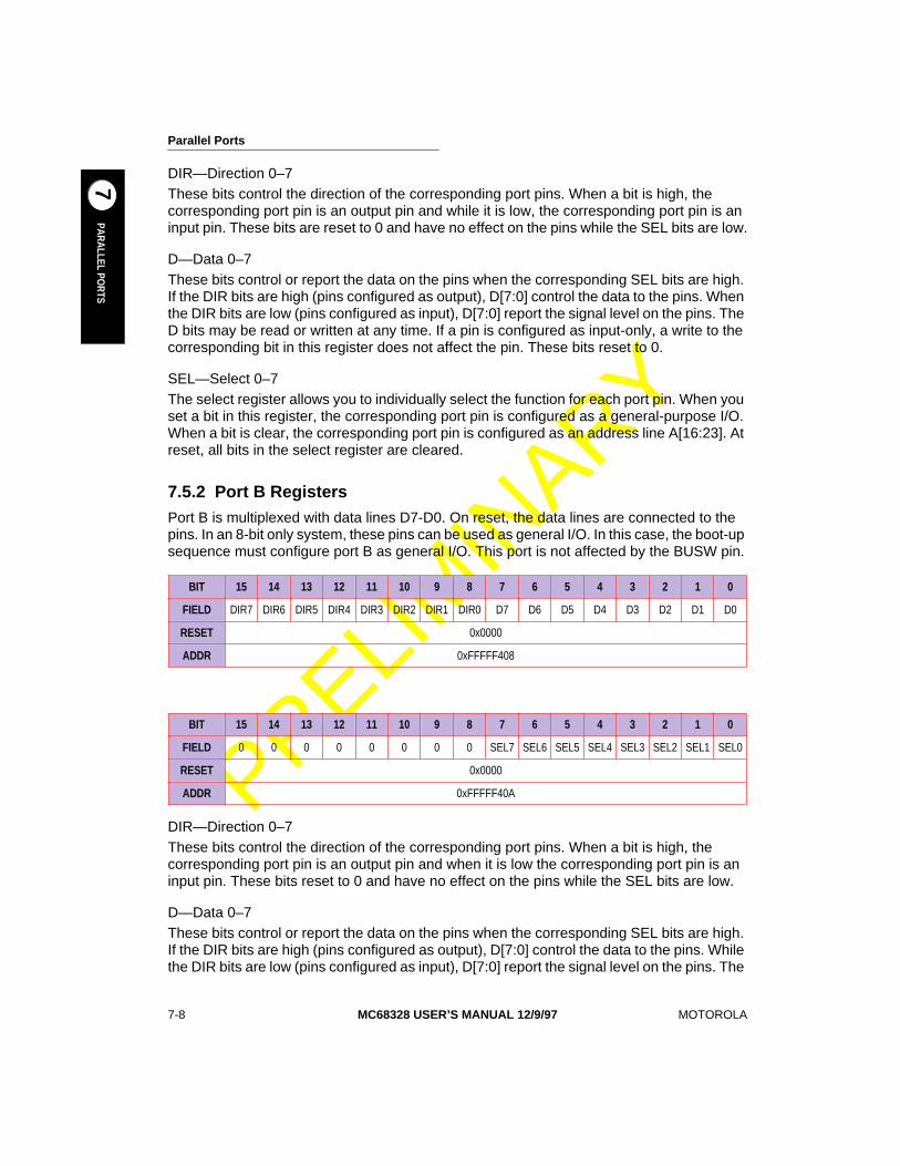
Parallel Ports
7-8
MC68328 USER’S MANUAL 12/9/97
MOTOROLA
PARALLEL PORTS
7
PRELIM
INARY
DIR—Direction 0–7These bits control the direction of the corresponding port pins. When a bit is high, the corresponding port pin is an output pin and while it is low, the corresponding port pin is an input pin. These bits are reset to 0 and have no effect on the pins while the SEL bits are low.
D—Data 0–7These bits control or report the data on the pins when the corresponding SEL bits are high. If the DIR bits are high (pins configured as output), D[7:0] control the data to the pins. When the DIR bits are low (pins configured as input), D[7:0] report the signal level on the pins. The D bits may be read or written at any time. If a pin is configured as input-only, a write to the corresponding bit in this register does not affect the pin. These bits reset to 0.
SEL—Select 0–7The select register allows you to individually select the function for each port pin. When you set a bit in this register, the corresponding port pin is configured as a general-purpose I/O. When a bit is clear, the corresponding port pin is configured as an address line A[16:23]. At reset, all bits in the select register are cleared.
7.5.2 Port B Registers
Port B is multiplexed with data lines D7-D0. On reset, the data lines are connected to the pins. In an 8-bit only system, these pins can be used as general I/O. In this case, the boot-up sequence must configure port B as general I/O. This port is not affected by the BUSW pin.
DIR—Direction 0–7These bits control the direction of the corresponding port pins. When a bit is high, the corresponding port pin is an output pin and when it is low the corresponding port pin is an input pin. These bits reset to 0 and have no effect on the pins while the SEL bits are low.
D—Data 0–7These bits control or report the data on the pins when the corresponding SEL bits are high. If the DIR bits are high (pins configured as output), D[7:0] control the data to the pins. While the DIR bits are low (pins configured as input), D[7:0] report the signal level on the pins. The
BIT 15 14 13 12 11 10 9 8 7 6 5 4 3 2 1 0
FIELD
DIR7 DIR6 DIR5 DIR4 DIR3 DIR2 DIR1 DIR0 D7 D6 D5 D4 D3 D2 D1 D0
RESET
0x0000
ADDR
0xFFFFF408
BIT 15 14 13 12 11 10 9 8 7 6 5 4 3 2 1 0
FIELD
0 0 0 0 0 0 0 0 SEL7 SEL6 SEL5 SEL4 SEL3 SEL2 SEL1 SEL0
RESET
0x0000
ADDR
0xFFFFF40A
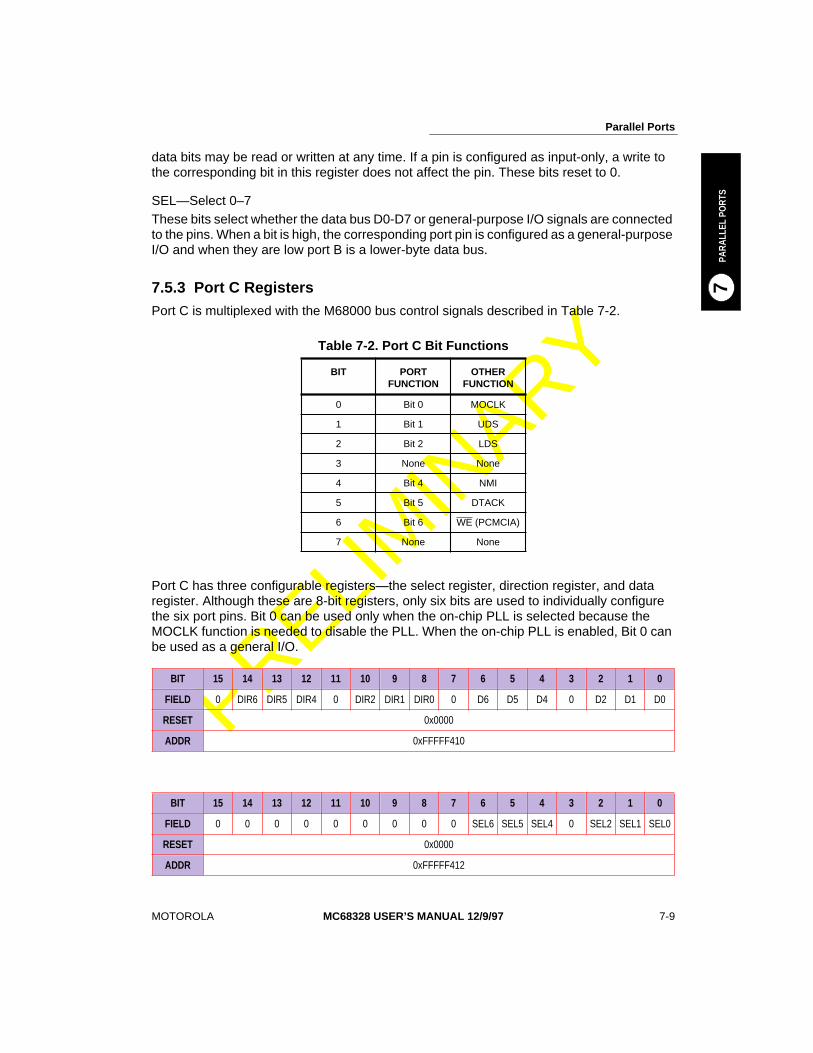
Parallel Ports
MOTOROLA
MC68328 USER’S MANUAL 12/9/97
7-9
PARA
LLEL
PO
RTS
7
PRELIM
INARY
data bits may be read or written at any time. If a pin is configured as input-only, a write to the corresponding bit in this register does not affect the pin. These bits reset to 0.
SEL—Select 0–7These bits select whether the data bus D0-D7 or general-purpose I/O signals are connected to the pins. When a bit is high, the corresponding port pin is configured as a general-purpose I/O and when they are low port B is a lower-byte data bus.
7.5.3 Port C Registers
Port C is multiplexed with the M68000 bus control signals described in Table 7-2.
Port C has three configurable registers—the select register, direction register, and data register. Although these are 8-bit registers, only six bits are used to individually configure the six port pins. Bit 0 can be used only when the on-chip PLL is selected because the MOCLK function is needed to disable the PLL. When the on-chip PLL is enabled, Bit 0 can be used as a general I/O.
Table 7-2. Port C Bit Functions
BIT PORT FUNCTION
OTHER FUNCTION
0 Bit 0 MOCLK
1 Bit 1 UDS
2 Bit 2 LDS
3 None None
4 Bit 4 NMI
5 Bit 5 DTACK
6 Bit 6 WE (PCMCIA)
7 None None
BIT 15 14 13 12 11 10 9 8 7 6 5 4 3 2 1 0
FIELD
0 DIR6 DIR5 DIR4 0 DIR2 DIR1 DIR0 0 D6 D5 D4 0 D2 D1 D0
RESET
0x0000
ADDR
0xFFFFF410
BIT 15 14 13 12 11 10 9 8 7 6 5 4 3 2 1 0
FIELD
0 0 0 0 0 0 0 0 0 SEL6 SEL5 SEL4 0 SEL2 SEL1 SEL0
RESET
0x0000
ADDR
0xFFFFF412
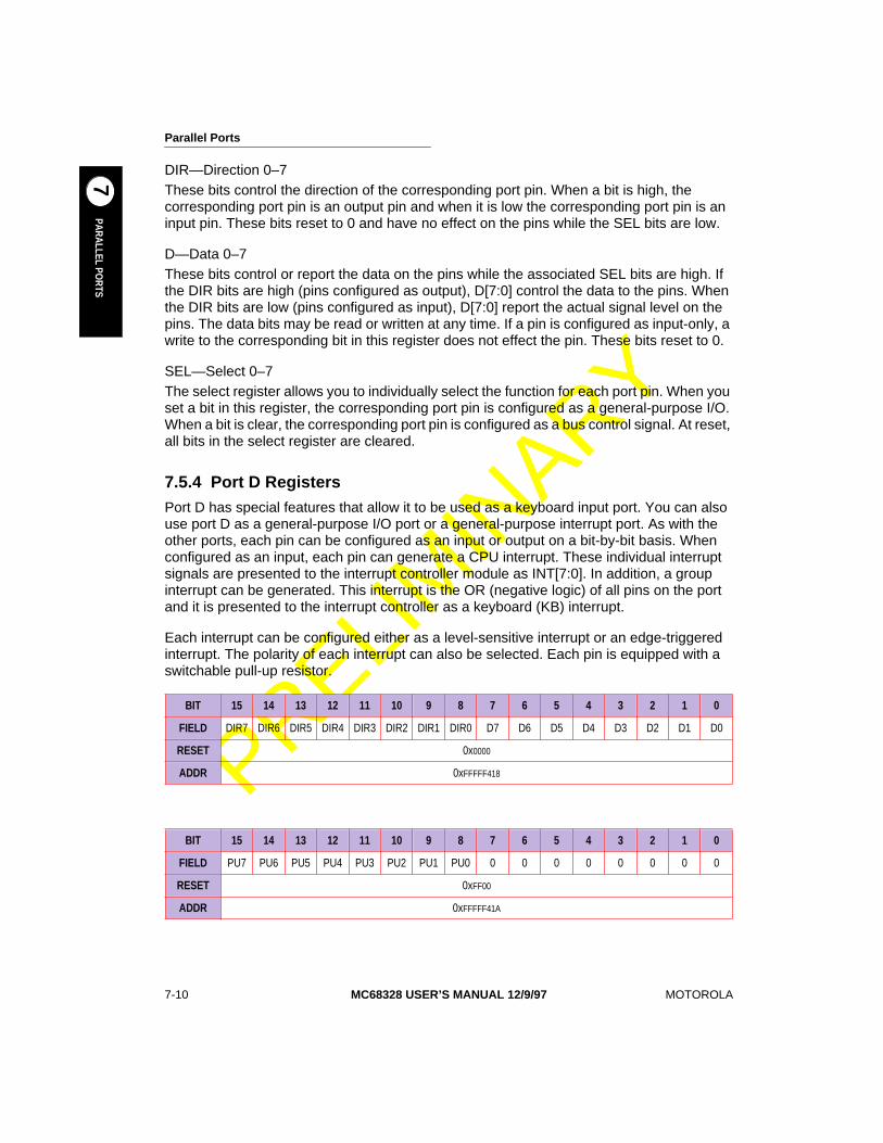
Parallel Ports
7-10
MC68328 USER’S MANUAL 12/9/97
MOTOROLA
PARALLEL PORTS
7
PRELIM
INARY
DIR—Direction 0–7These bits control the direction of the corresponding port pin. When a bit is high, the corresponding port pin is an output pin and when it is low the corresponding port pin is an input pin. These bits reset to 0 and have no effect on the pins while the SEL bits are low.
D—Data 0–7These bits control or report the data on the pins while the associated SEL bits are high. If the DIR bits are high (pins configured as output), D[7:0] control the data to the pins. When the DIR bits are low (pins configured as input), D[7:0] report the actual signal level on the pins. The data bits may be read or written at any time. If a pin is configured as input-only, a write to the corresponding bit in this register does not effect the pin. These bits reset to 0.
SEL—Select 0–7The select register allows you to individually select the function for each port pin. When you set a bit in this register, the corresponding port pin is configured as a general-purpose I/O. When a bit is clear, the corresponding port pin is configured as a bus control signal. At reset, all bits in the select register are cleared.
7.5.4 Port D Registers
Port D has special features that allow it to be used as a keyboard input port. You can also use port D as a general-purpose I/O port or a general-purpose interrupt port. As with the other ports, each pin can be configured as an input or output on a bit-by-bit basis. When configured as an input, each pin can generate a CPU interrupt. These individual interrupt signals are presented to the interrupt controller module as INT[7:0]. In addition, a group interrupt can be generated. This interrupt is the OR (negative logic) of all pins on the port and it is presented to the interrupt controller as a keyboard (KB) interrupt.
Each interrupt can be configured either as a level-sensitive interrupt or an edge-triggered interrupt. The polarity of each interrupt can also be selected. Each pin is equipped with a switchable pull-up resistor.
BIT 15 14 13 12 11 10 9 8 7 6 5 4 3 2 1 0
FIELD
DIR7 DIR6 DIR5 DIR4 DIR3 DIR2 DIR1 DIR0 D7 D6 D5 D4 D3 D2 D1 D0
RESET
0x
0000
ADDR
0x
FFFFF418
BIT 15 14 13 12 11 10 9 8 7 6 5 4 3 2 1 0
FIELD
PU7 PU6 PU5 PU4 PU3 PU2 PU1 PU0 0 0 0 0 0 0 0 0
RESET
0x
FF00
ADDR
0x
FFFFF41A

Parallel Ports
MOTOROLA
MC68328 USER’S MANUAL 12/9/97
7-11
PARA
LLEL
PO
RTS
7PRELI
MIN
ARYDIR—Direction 0–7These bits control the direction of the corresponding port pin. When a bit is high, the corresponding port pin is an output pin and when it is low, the corresponding port pin is an input pin. At reset, these bits default to 0.
D—Data 0–7These bits control or report the data on the pins. When the DIR bits are high, D[7:0] control the data to the pins. Data can be read or written to any bit. While the DIR bits are low, D[7:0] report the signal level on the pins. In this case, writing to a read-only bit does not affect the pin. Notice that the actual value on the pin is reported when a pin is read. Bits that are configured as edge-sensitive interrupts will read 1 when an edge is detected. The interrupt is cleared by writing a 1 to the set bit.
PU—Pull-Up 0–7These bits enable the pull-up resistors on the port. When a bit is set in this register, the pull-up is enabled for the corresponding port pin. When a bit is cleared, the pull-up is disabled. At reset, all pull-ups are enabled for this port.
POL—Polarity 0–7These bits select the input signal polarity. When the bits are high, the input data is inverted before it is presented to the holding register and when the bits are low, the data is presented as is. Interrupts are active-high (or rising edge) while these bits are low. Interrupts are active-low (or falling edge) while these bits are high.
BIT 15 14 13 12 11 10 9 8 7 6 5 4 3 2 1 0
FIELD POL7 POL6 POL5 POL4 POL3 POL2 POL1 POL0 IQEN7 IQEN6 IQEN5 IQEN4 IQEN3 IQEN2 IQEN1 IQEN0
RESET 0x0000
ADDR 0xFFFFF41C
BIT 15 14 13 12 11 10 9 8 7 6 5 4 3 2 1 0
FIELD 0 0 0 0 0 0 0 0 IQEG7 IQEG6 IQEG5 IQEG4 IQEG3 IQEG2 IQEG1 IQEG0
RESET 0x0000
ADDR 0xFFFFF41E
Note: Port D edge interrupts cannot generate wake-up events when the chip is in sleep mode.
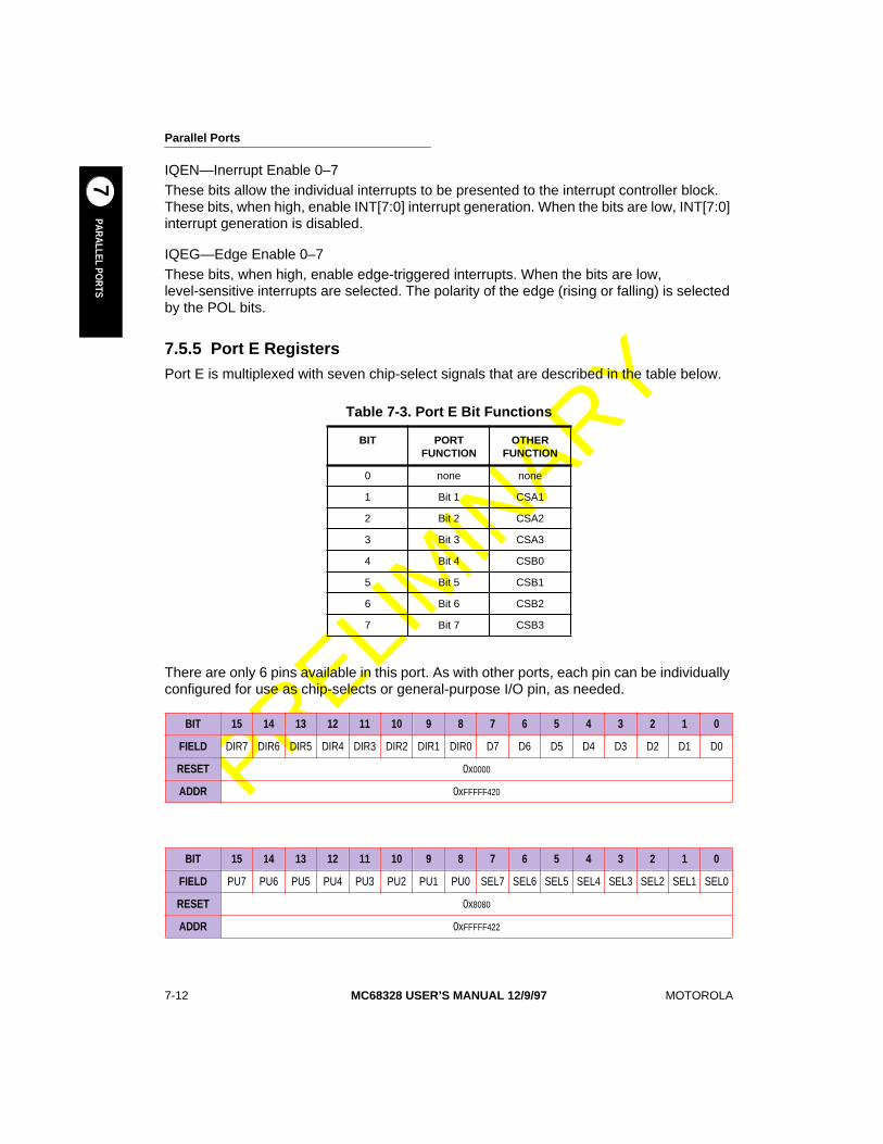
Parallel Ports
7-12 MC68328 USER’S MANUAL 12/9/97 MOTOROLA
PARALLEL PORTS
7PRELI
MIN
ARY
IQEN—Inerrupt Enable 0–7These bits allow the individual interrupts to be presented to the interrupt controller block. These bits, when high, enable INT[7:0] interrupt generation. When the bits are low, INT[7:0] interrupt generation is disabled.
IQEG—Edge Enable 0–7These bits, when high, enable edge-triggered interrupts. When the bits are low, level-sensitive interrupts are selected. The polarity of the edge (rising or falling) is selected by the POL bits.
7.5.5 Port E RegistersPort E is multiplexed with seven chip-select signals that are described in the table below.
There are only 6 pins available in this port. As with other ports, each pin can be individually configured for use as chip-selects or general-purpose I/O pin, as needed.
Table 7-3. Port E Bit Functions
BIT PORT FUNCTION
OTHER FUNCTION
0 none none
1 Bit 1 CSA1
2 Bit 2 CSA2
3 Bit 3 CSA3
4 Bit 4 CSB0
5 Bit 5 CSB1
6 Bit 6 CSB2
7 Bit 7 CSB3
BIT 15 14 13 12 11 10 9 8 7 6 5 4 3 2 1 0
FIELD DIR7 DIR6 DIR5 DIR4 DIR3 DIR2 DIR1 DIR0 D7 D6 D5 D4 D3 D2 D1 D0
RESET 0x0000
ADDR 0xFFFFF420
BIT 15 14 13 12 11 10 9 8 7 6 5 4 3 2 1 0
FIELD PU7 PU6 PU5 PU4 PU3 PU2 PU1 PU0 SEL7 SEL6 SEL5 SEL4 SEL3 SEL2 SEL1 SEL0
RESET 0x8080
ADDR 0xFFFFF422
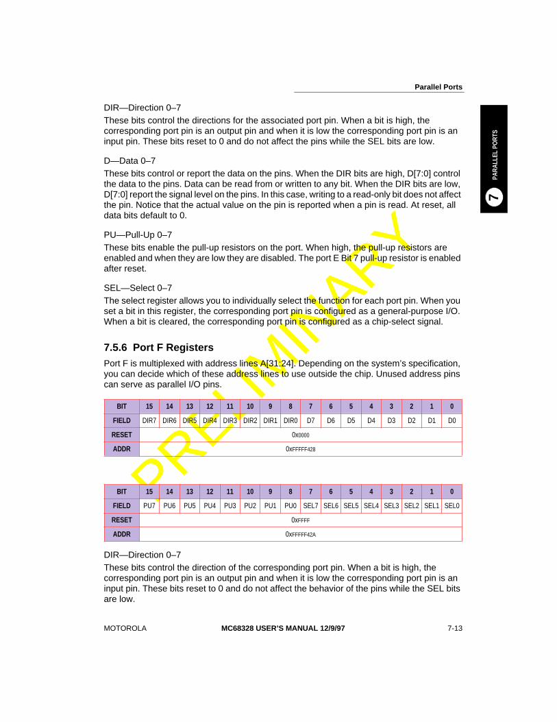
Parallel Ports
MOTOROLA MC68328 USER’S MANUAL 12/9/97 7-13
PARA
LLEL
PO
RTS
7PRELI
MIN
ARY
DIR—Direction 0–7These bits control the directions for the associated port pin. When a bit is high, the corresponding port pin is an output pin and when it is low the corresponding port pin is an input pin. These bits reset to 0 and do not affect the pins while the SEL bits are low.
D—Data 0–7These bits control or report the data on the pins. When the DIR bits are high, D[7:0] control the data to the pins. Data can be read from or written to any bit. When the DIR bits are low, D[7:0] report the signal level on the pins. In this case, writing to a read-only bit does not affect the pin. Notice that the actual value on the pin is reported when a pin is read. At reset, all data bits default to 0.
PU—Pull-Up 0–7These bits enable the pull-up resistors on the port. When high, the pull-up resistors are enabled and when they are low they are disabled. The port E Bit 7 pull-up resistor is enabled after reset.
SEL—Select 0–7The select register allows you to individually select the function for each port pin. When you set a bit in this register, the corresponding port pin is configured as a general-purpose I/O. When a bit is cleared, the corresponding port pin is configured as a chip-select signal.
7.5.6 Port F RegistersPort F is multiplexed with address lines A[31:24]. Depending on the system’s specification, you can decide which of these address lines to use outside the chip. Unused address pins can serve as parallel I/O pins.
DIR—Direction 0–7These bits control the direction of the corresponding port pin. When a bit is high, the corresponding port pin is an output pin and when it is low the corresponding port pin is an input pin. These bits reset to 0 and do not affect the behavior of the pins while the SEL bits are low.
BIT 15 14 13 12 11 10 9 8 7 6 5 4 3 2 1 0
FIELD DIR7 DIR6 DIR5 DIR4 DIR3 DIR2 DIR1 DIR0 D7 D6 D5 D4 D3 D2 D1 D0
RESET 0x0000
ADDR 0xFFFFF428
BIT 15 14 13 12 11 10 9 8 7 6 5 4 3 2 1 0
FIELD PU7 PU6 PU5 PU4 PU3 PU2 PU1 PU0 SEL7 SEL6 SEL5 SEL4 SEL3 SEL2 SEL1 SEL0
RESET 0xFFFF
ADDR 0xFFFFF42A
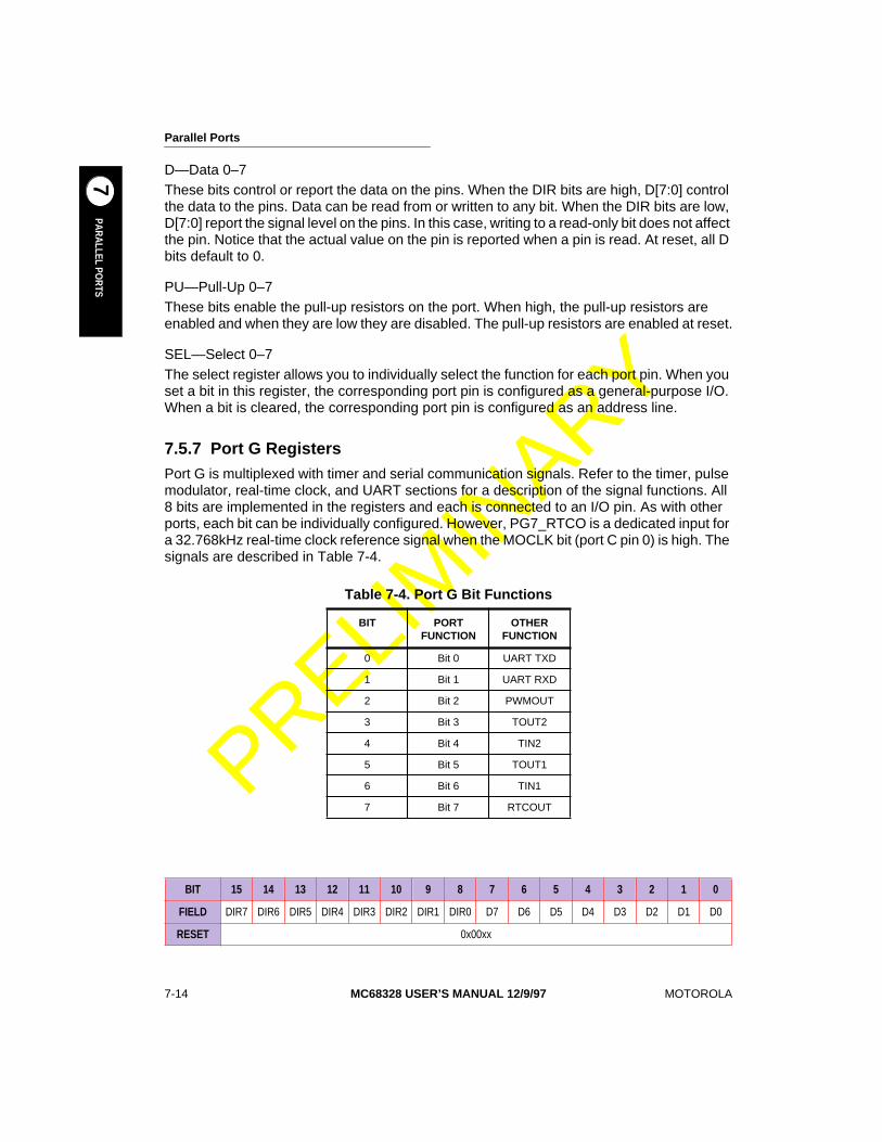
Parallel Ports
7-14 MC68328 USER’S MANUAL 12/9/97 MOTOROLA
PARALLEL PORTS
7PRELI
MIN
ARY
D—Data 0–7These bits control or report the data on the pins. When the DIR bits are high, D[7:0] control the data to the pins. Data can be read from or written to any bit. When the DIR bits are low, D[7:0] report the signal level on the pins. In this case, writing to a read-only bit does not affect the pin. Notice that the actual value on the pin is reported when a pin is read. At reset, all D bits default to 0.
PU—Pull-Up 0–7These bits enable the pull-up resistors on the port. When high, the pull-up resistors are enabled and when they are low they are disabled. The pull-up resistors are enabled at reset.
SEL—Select 0–7The select register allows you to individually select the function for each port pin. When you set a bit in this register, the corresponding port pin is configured as a general-purpose I/O. When a bit is cleared, the corresponding port pin is configured as an address line.
7.5.7 Port G RegistersPort G is multiplexed with timer and serial communication signals. Refer to the timer, pulse modulator, real-time clock, and UART sections for a description of the signal functions. All 8 bits are implemented in the registers and each is connected to an I/O pin. As with other ports, each bit can be individually configured. However, PG7_RTCO is a dedicated input for a 32.768kHz real-time clock reference signal when the MOCLK bit (port C pin 0) is high. The signals are described in Table 7-4.
Table 7-4. Port G Bit Functions
BIT PORT FUNCTION
OTHER FUNCTION
0 Bit 0 UART TXD
1 Bit 1 UART RXD
2 Bit 2 PWMOUT
3 Bit 3 TOUT2
4 Bit 4 TIN2
5 Bit 5 TOUT1
6 Bit 6 TIN1
7 Bit 7 RTCOUT
BIT 15 14 13 12 11 10 9 8 7 6 5 4 3 2 1 0
FIELD DIR7 DIR6 DIR5 DIR4 DIR3 DIR2 DIR1 DIR0 D7 D6 D5 D4 D3 D2 D1 D0
RESET 0x00xx
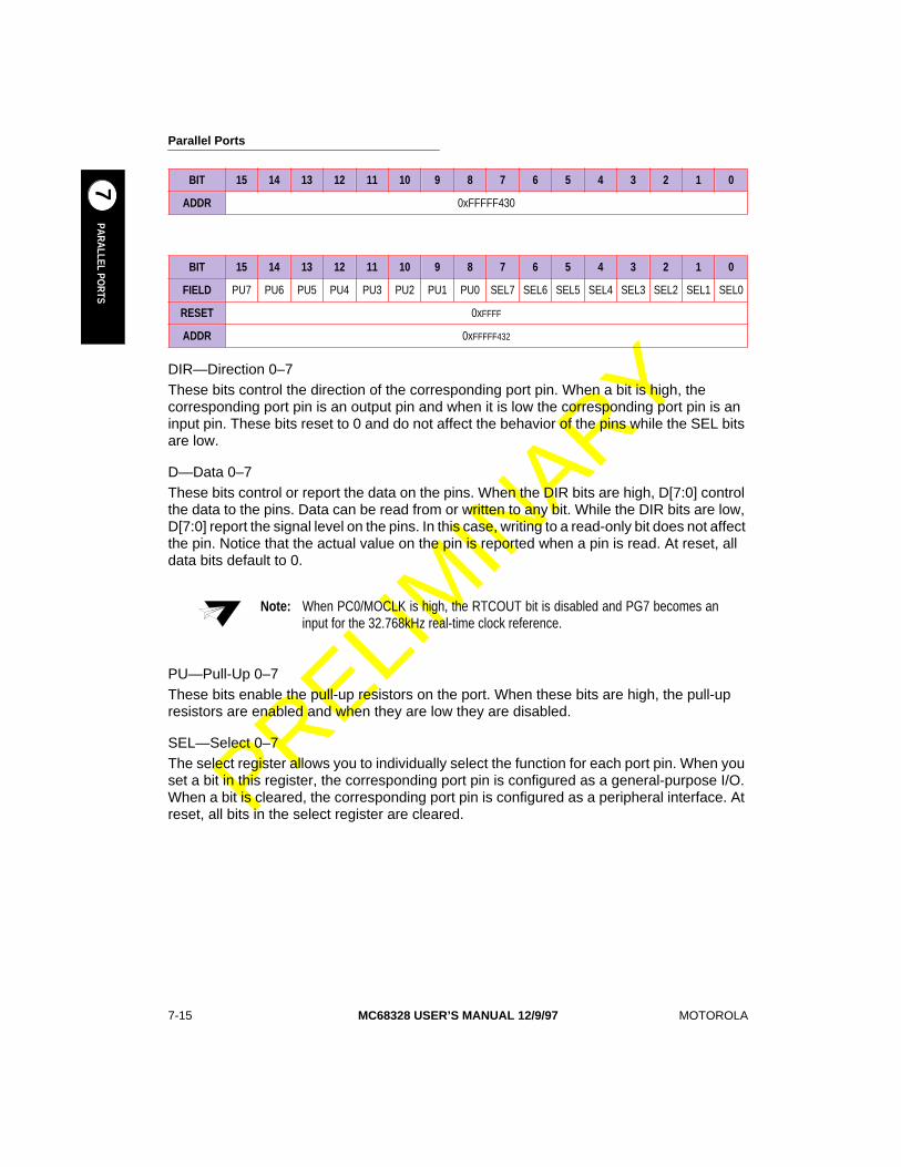
Parallel Ports
7-15 MC68328 USER’S MANUAL 12/9/97 MOTOROLA
PARALLEL PORTS
7PRELI
MIN
ARYDIR—Direction 0–7These bits control the direction of the corresponding port pin. When a bit is high, the corresponding port pin is an output pin and when it is low the corresponding port pin is an input pin. These bits reset to 0 and do not affect the behavior of the pins while the SEL bits are low.
D—Data 0–7These bits control or report the data on the pins. When the DIR bits are high, D[7:0] control the data to the pins. Data can be read from or written to any bit. While the DIR bits are low, D[7:0] report the signal level on the pins. In this case, writing to a read-only bit does not affect the pin. Notice that the actual value on the pin is reported when a pin is read. At reset, all data bits default to 0.
PU—Pull-Up 0–7These bits enable the pull-up resistors on the port. When these bits are high, the pull-up resistors are enabled and when they are low they are disabled.
SEL—Select 0–7The select register allows you to individually select the function for each port pin. When you set a bit in this register, the corresponding port pin is configured as a general-purpose I/O. When a bit is cleared, the corresponding port pin is configured as a peripheral interface. At reset, all bits in the select register are cleared.
ADDR 0xFFFFF430
BIT 15 14 13 12 11 10 9 8 7 6 5 4 3 2 1 0
FIELD PU7 PU6 PU5 PU4 PU3 PU2 PU1 PU0 SEL7 SEL6 SEL5 SEL4 SEL3 SEL2 SEL1 SEL0
RESET 0xFFFF
ADDR 0xFFFFF432
Note: When PC0/MOCLK is high, the RTCOUT bit is disabled and PG7 becomes aninput for the 32.768kHz real-time clock reference.
BIT 15 14 13 12 11 10 9 8 7 6 5 4 3 2 1 0
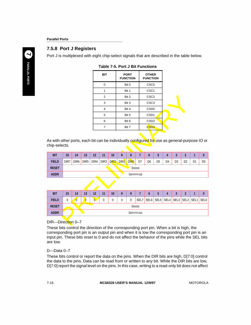
Parallel Ports
7-16 MC68328 USER’S MANUAL 12/9/97 MOTOROLA
PARALLEL PORTS
7PRELI
MIN
ARY
7.5.8 Port J RegistersPort J is multiplexed with eight chip-select signals that are described in the table below.
As with other ports, each bit can be individually configured for use as general-purpose IO or chip-selects.
DIR—Direction 0–7These bits control the direction of the corresponding port pin. When a bit is high, the corresponding port pin is an output pin and when it is low the corresponding port pin is an input pin. These bits reset to 0 and do not affect the behavior of the pins while the SEL bits are low.
D—Data 0–7These bits control or report the data on the pins. When the DIR bits are high, D[7:0] control the data to the pins. Data can be read from or written to any bit. While the DIR bits are low, D[7:0] report the signal level on the pins. In this case, writing to a read-only bit does not affect
Table 7-5. Port J Bit Functions
BIT PORT FUNCTION
OTHER FUNCTION
0 Bit 0 CSC0
1 Bit 1 CSC1
2 Bit 2 CSC2
3 Bit 3 CSC3
4 Bit 4 CSD0
5 Bit 5 CSD1
6 Bit 6 CSD2
7 Bit 7 CSD3
BIT 15 14 13 12 11 10 9 8 7 6 5 4 3 2 1 0
FIELD DIR7 DIR6 DIR5 DIR4 DIR3 DIR2 DIR1 DIR0 D7 D6 D5 D4 D3 D2 D1 D0
RESET 0x0000
ADDR 0xFFFFF438
BIT 15 14 13 12 11 10 9 8 7 6 5 4 3 2 1 0
FIELD 0 0 0 0 0 0 0 0 SEL7 SEL6 SEL5 SEL4 SEL3 SEL2 SEL1 SEL0
RESET 0x0000
ADDR 0xFFFFF43A
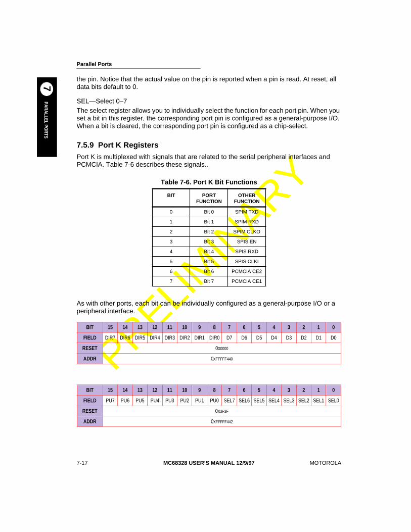
Parallel Ports
7-17 MC68328 USER’S MANUAL 12/9/97 MOTOROLA
PARALLEL PORTS
7PRELI
MIN
ARY
the pin. Notice that the actual value on the pin is reported when a pin is read. At reset, all data bits default to 0.
SEL—Select 0–7The select register allows you to individually select the function for each port pin. When you set a bit in this register, the corresponding port pin is configured as a general-purpose I/O. When a bit is cleared, the corresponding port pin is configured as a chip-select.
7.5.9 Port K RegistersPort K is multiplexed with signals that are related to the serial peripheral interfaces and PCMCIA. Table 7-6 describes these signals..
As with other ports, each bit can be individually configured as a general-purpose I/O or a peripheral interface.
Table 7-6. Port K Bit Functions
BIT PORT FUNCTION
OTHER FUNCTION
0 Bit 0 SPIM TXD
1 Bit 1 SPIM RXD
2 Bit 2 SPIM CLKO
3 Bit 3 SPIS EN
4 Bit 4 SPIS RXD
5 Bit 5 SPIS CLKI
6 Bit 6 PCMCIA CE2
7 Bit 7 PCMCIA CE1
BIT 15 14 13 12 11 10 9 8 7 6 5 4 3 2 1 0
FIELD DIR7 DIR6 DIR5 DIR4 DIR3 DIR2 DIR1 DIR0 D7 D6 D5 D4 D3 D2 D1 D0
RESET 0x0000
ADDR 0xFFFFF440
BIT 15 14 13 12 11 10 9 8 7 6 5 4 3 2 1 0
FIELD PU7 PU6 PU5 PU4 PU3 PU2 PU1 PU0 SEL7 SEL6 SEL5 SEL4 SEL3 SEL2 SEL1 SEL0
RESET 0x3F3F
ADDR 0xFFFFF442
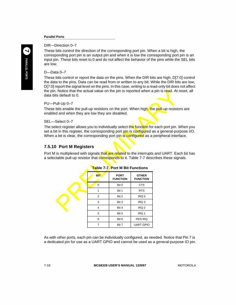
Parallel Ports
7-18 MC68328 USER’S MANUAL 12/9/97 MOTOROLA
PARALLEL PORTS
7PRELI
MIN
ARY
DIR—Direction 0–7These bits control the direction of the corresponding port pin. When a bit is high, the corresponding port pin is an output pin and when it is low the corresponding port pin is an input pin. These bits reset to 0 and do not affect the behavior of the pins while the SEL bits are low.
D—Data 0–7These bits control or report the data on the pins. When the DIR bits are high, D[7:0] control the data to the pins. Data can be read from or written to any bit. While the DIR bits are low, D[7:0] report the signal level on the pins. In this case, writing to a read-only bit does not affect the pin. Notice that the actual value on the pin is reported when a pin is read. At reset, all data bits default to 0.
PU—Pull-Up 0–7These bits enable the pull-up resistors on the port. When high, the pull-up resistors are enabled and when they are low they are disabled.
SEL—Select 0–7The select register allows you to individually select the function for each port pin. When you set a bit in this register, the corresponding port pin is configured as a general-purpose I/O. When a bit is clear, the corresponding port pin is configured as a peripheral interface.
7.5.10 Port M RegistersPort M is multiplexed with signals that are related to the interrupts and UART. Each bit has a selectable pull-up resistor that corresponds to it. Table 7-7 describes these signals.
As with other ports, each pin can be individually configured, as needed. Notice that Pin 7 is a dedicated pin for use as a UART GPIO and cannot be used as a general-purpose IO pin.
Table 7-7. Port M Bit Functions
BIT PORT FUNCTION
OTHER FUNCTION
0 Bit 0 CTS
1 Bit 1 RTS
2 Bit 2 IRQ 6
3 Bit 3 IRQ 3
4 Bit 4 IRQ 2
5 Bit 5 IRQ 1
6 Bit 6 PEN IRQ
7 Bit 7 UART GPIO
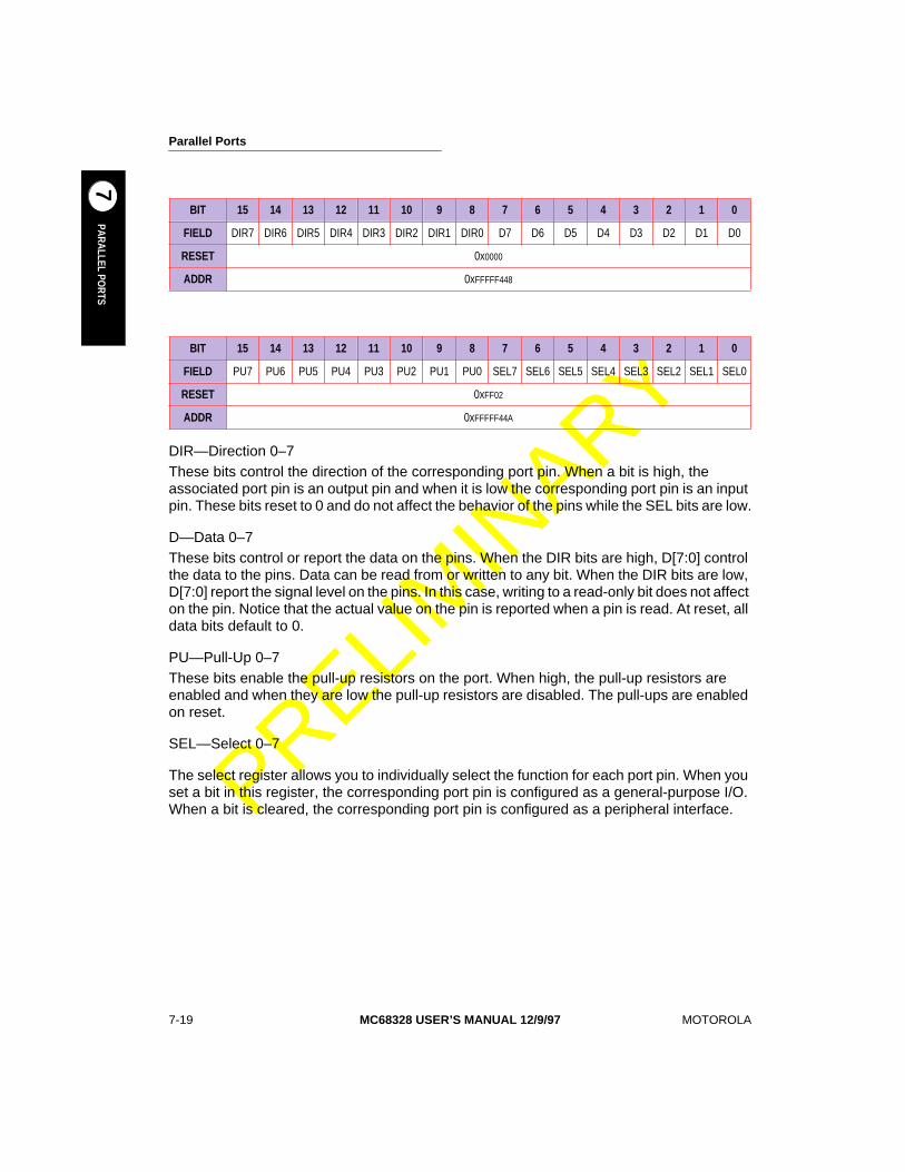
Parallel Ports
7-19 MC68328 USER’S MANUAL 12/9/97 MOTOROLA
PARALLEL PORTS
7PRELI
MIN
ARYDIR—Direction 0–7These bits control the direction of the corresponding port pin. When a bit is high, the associated port pin is an output pin and when it is low the corresponding port pin is an input pin. These bits reset to 0 and do not affect the behavior of the pins while the SEL bits are low.
D—Data 0–7These bits control or report the data on the pins. When the DIR bits are high, D[7:0] control the data to the pins. Data can be read from or written to any bit. When the DIR bits are low, D[7:0] report the signal level on the pins. In this case, writing to a read-only bit does not affect on the pin. Notice that the actual value on the pin is reported when a pin is read. At reset, all data bits default to 0.
PU—Pull-Up 0–7These bits enable the pull-up resistors on the port. When high, the pull-up resistors are enabled and when they are low the pull-up resistors are disabled. The pull-ups are enabled on reset.
SEL—Select 0–7
The select register allows you to individually select the function for each port pin. When you set a bit in this register, the corresponding port pin is configured as a general-purpose I/O. When a bit is cleared, the corresponding port pin is configured as a peripheral interface.
BIT 15 14 13 12 11 10 9 8 7 6 5 4 3 2 1 0
FIELD DIR7 DIR6 DIR5 DIR4 DIR3 DIR2 DIR1 DIR0 D7 D6 D5 D4 D3 D2 D1 D0
RESET 0x0000
ADDR 0xFFFFF448
BIT 15 14 13 12 11 10 9 8 7 6 5 4 3 2 1 0
FIELD PU7 PU6 PU5 PU4 PU3 PU2 PU1 PU0 SEL7 SEL6 SEL5 SEL4 SEL3 SEL2 SEL1 SEL0
RESET 0xFF02
ADDR 0xFFFFF44A

Parallel Ports
7-20 MC68328 USER’S MANUAL 12/9/97 MOTOROLA
PARALLEL PORTS
7PRELI
MIN
ARY
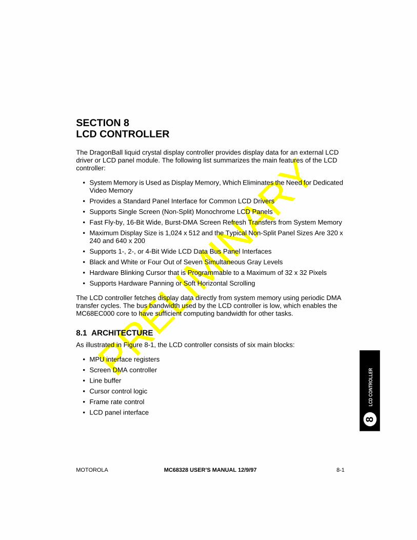
MOTOROLA
MC68328 USER’S MANUAL 12/9/97
8-1
LCD
CONT
ROLL
ER
8
PRELIM
INARY
SECTION 8LCD CONTROLLER
The DragonBall liquid crystal display controller provides display data for an external LCD driver or LCD panel module. The following list summarizes the main features of the LCD controller:
• System Memory is Used as Display Memory, Which Eliminates the Need for Dedicated Video Memory
• Provides a Standard Panel Interface for Common LCD Drivers
• Supports Single Screen (Non-Split) Monochrome LCD Panels
• Fast Fly-by, 16-Bit Wide, Burst-DMA Screen Refresh Transfers from System Memory
• Maximum Display Size is 1,024 x 512 and the Typical Non-Split Panel Sizes Are 320 x 240 and 640 x 200
• Supports 1-, 2-, or 4-Bit Wide LCD Data Bus Panel Interfaces
• Black and White or Four Out of Seven Simultaneous Gray Levels
• Hardware Blinking Cursor that is Programmable to a Maximum of 32 x 32 Pixels
• Supports Hardware Panning or Soft Horizontal Scrolling
The LCD controller fetches display data directly from system memory using periodic DMA transfer cycles. The bus bandwidth used by the LCD controller is low, which enables the MC68EC000 core to have sufficient computing bandwidth for other tasks.
8.1 ARCHITECTURE
As illustrated in Figure 8-1, the LCD controller consists of six main blocks:
• MPU interface registers
• Screen DMA controller
• Line buffer
• Cursor control logic
• Frame rate control
• LCD panel interface
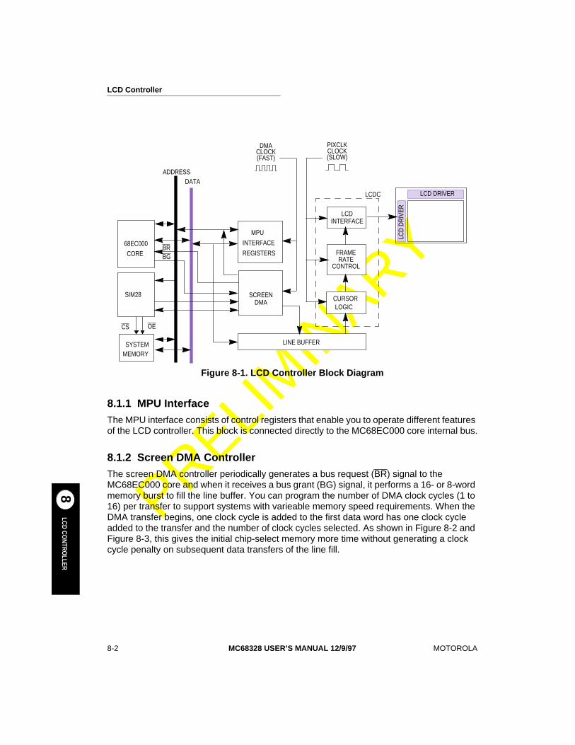
LCD Controller
8-2
MC68328 USER’S MANUAL 12/9/97
MOTOROLA
LCD CONTRO
LLER
8
PRELIM
INARY
8.1.1 MPU Interface
The MPU interface consists of control registers that enable you to operate different features of the LCD controller. This block is connected directly to the MC68EC000 core internal bus.
8.1.2 Screen DMA Controller
The screen DMA controller periodically generates a bus request (BR) signal to the MC68EC000 core and when it receives a bus grant (BG) signal, it performs a 16- or 8-word memory burst to fill the line buffer. You can program the number of DMA clock cycles (1 to 16) per transfer to support systems with varieable memory speed requirements. When the DMA transfer begins, one clock cycle is added to the first data word has one clock cycle added to the transfer and the number of clock cycles selected. As shown in Figure 8-2 and Figure 8-3, this gives the initial chip-select memory more time without generating a clock cycle penalty on subsequent data transfers of the line fill.
Figure 8-1. LCD Controller Block Diagram
SCREENDMA
LINE BUFFER
FRAMERATE
CONTROL
PIXCLKDMA
SYSTEM
68EC000
LCD DRIVER
LCD
DR
IVER
CLOCKCLOCK
ADDRESSDATA
LCDINTERFACE
(FAST) (SLOW)
LCDC
CURSORLOGIC
CORE
CS
MEMORY
MPU
INTERFACE
REGISTERSBRBG
SIM28
OE
LCD Controller
MOTOROLA
MC68328 USER’S MANUAL 12/9/97
8-3
LCD
CONT
ROLL
ER
8
PRELIM
INARY
8.1.3 Line Buffer
The line buffer collects display data from system memory during DMA cycles and outputs it to the cursor control logic. The input is synchronized with the fast DMA clock and the output is synchronized to the relatively slow LCD pixel clock (PIXCLK).
8.1.4 Cursor Logic
When enabled, the cursor control logic generates a block-shaped cursor on the display screen. You can adjust the cursor height and width anywhere between 1 and 31 pixel counts. The cursor can be black or it can be in reversed video. The blinking rate is adjustable when the blink enable bit is set.
8.1.5 Frame Rate Control
The frame rate control (FRC) is primarily used for a grayscale display and can generate a maximum of four gray levels out of seven density levels (0, 1/4, 5/16, 1/2, 11/16, 3/4, 1 as shown in Table 8-2). The density level corresponds to the number of times the pixel is being turned on when the display is refreshed frame by frame. Since the crystal formulations and driving voltage may vary, you can tune the visual gray quality by programming the LCD gray palette-mapping register (LGPMR) to obtain the best effect.
Blinking or flickering will occur if all LCD pixel cells are synchronized, so you must program two 4-bit numbers (XOFF and YOFF in the FRC offset register). As a general rule, select odd numbers that differ by two. Different inter-pixel crosstalk characteristics cause the optimal offset values to vary among different types of LCD panels (even from the same manufacturer).
8.1.6 LCD Panel Interface
The LCD panel interface logic packs the display data in the correct size and outputs it to the LCD panel data bus. You can program the polarity of the FRM, LP, and SCLK signals, as well as pixel data, for different types of LCD panels.
LCD Controller
8-4
MC68328 USER’S MANUAL 12/9/97
MOTOROLA
LCD CONTRO
LLER
8
PRELIM
INARY
8.2 OPERATION
The LCD’s DMA controller is a fly-by 16-bit wide, fast-data transfer machine. The LCD screen has to be refreshed continuously at a rate of approximately 50-70Hz, which means the image data in memory is periodically read and transferred to the corresponding pixels on the screen. The refresh is divided into small bursts of 8- or 16-word reads. When the internal line buffer needs data, it asserts the BR signal to request the bus from the core. Once the core grants the bus by asserting the BG signal, the DMA controller gets control of the bus signal and issues 8- or 16-word reads from memory. During LCD access cycles, the chip-select logic asserts the output enable and chip-select signals for the corresponding system memory chip inside the system integration module. You can achieve the minimum bus bandwidth obstruction by using zero LCD access wait states (1 clock per access). See
Section 8.9 Calculating Bandwidth
for more information.
8.2.1 DMA
As shown in Figure 8-2 and Figure 8-3, data is efficiently fetched from memory. Each burst is limited to 8/16 words, which reduces the possible latency for other peripherals, such as the interrupt controller. For example, the average latency for LCDCLK = 5MHz with a 16-word burst is approximately 2.4µs.
Figure 8-2. Three Clocks per LCD DMA Transfer (Two Wait States)
SYSCLK
INTERNAL BR
INTERNAL BG
ADDRESS
DATA
OE
CS
LCD Controller
MOTOROLA
MC68328 USER’S MANUAL 12/9/97
8-5
LCD
CONT
ROLL
ER
8
PRELIM
INARY
To operate, the DMA begins with an internal bus request from the DMA to the core and a bus grant to the DMA controller when the processor has given up the bus. The DMA cycle on the bus begins with chip-select assertion and addressing for the first data word to be transferred. A DMA cycle is indicated on the bus when a chip select is asserted with AS negated.
One clock cycle is added to the first data transfer of the DMA to allow for chip-select access time. For example, if the number of clock cycles selected for each DMA data word transfer is two, the first data word would transfer in three clocks. Subsequent data word transfers occur in two clock cycles to the end of the DMA burst. If the number of wait-states selected is zero, the DMA controller will complete each data transaction of the DMA burst in one clock with the exception of the first data word transfer, which occurs in two clocks as shown in Figure 8-6.
When the DMA controller has filled the line buffer, it negates the internal BR signal and relinquishes the bus to the core. If the core is in sleep mode, the internal bus is always granted to the DMA controller, which allows LCD images to be displayed while saving system power.
Figure 8-3. One Clock per DMA Transfer (0 Wait States)
SYSCLK
INTERNAL BR
INTERNAL BG
ADDRESS
DATA
OE
CS
LCD Controller
8-6
MC68328 USER’S MANUAL 12/9/97
MOTOROLA
LCD CONTRO
LLER
8
PRELIM
INARY
8.2.2 Interfacing the LCD Controller with an LCD Panel
With the following signals, you can interface the LCD controller to an LCD panel.
8.2.2.1 LCD DATA BUS SIGNALS.
The LD3–LD0 signals output bus transfers pixel data to the LCD panel for display. Data is arranged differently on the bus depending on the LCD data-width mode selected, as shown in Figure 8-3. System software can also program the output pixel data to be inverted. See
Section 8.6.2 LCD Polarity Configuration Register
for more information.
The LCD data bus uses LD0 to display pixel 0, 0. Some LCD panel manufacturers specify their LCD panel data bus in which data bit 3 of the panel displays pixel 0,0. For these panels, connections from the DragonBall’s LD bus to the LCD panel data bus are reversed in bit significance (LD3 connects to panel data 0, LD2 to panel data 1, LD1 to panel data 2, and LD0 to panel data 3).
8.2.2.2 LCD FIRST LINE MARKER SIGNAL.
The LFLM signal indicates the start of a new display frame. It becomes active after the first line pulse of the frame and remains active until the next line pulse, at which point it deasserts and remains inactive until the next frame. You can program the LFLM signal to be active-high or active-low. See
Section 8.6.2 LCD Polarity Configuration Register
for details.
8.2.2.3 LINE PULSE SIGNAL.
The LP signal latches a line of shifted data into the LCD panel. It becomes active when a line of pixel data is clocked into the LCD panel and stays asserted for a duration of eight pixel clock periods. You can program the LP signal to be either active-high or active-low. See
Section 8.6.2 LCD Polarity Configuration Register
for details.
8.2.2.4 LCD SHIFT CLOCK SIGNAL.
The LSCLK signal is the clock output that is synchronized to the LCD panel output data. Your system software can program the LSCLK signal to be either active-high or active-low. See
Section 8.6.2 LCD Polarity Configuration Register
for details.
8.2.2.5 LCD ALTERNATE CRYSTAL DIRECTION SIGNAL.
The LACD output signal is toggled to alternate the crystal polarization of the panel. This provides an AC polarity change that prevents crystal degradation of the LCD panel caused by DC voltage. Your system software can program this signal to toggle at a 1 to 16 frame period. The alternate crystal direction (LACD or M) pin will toggle after the preprogrammed number of FLM pulses. Your system software can also program the ACD rate control register (LACDRC) so that LACD will toggle once every 1–16 frames. The targeted number of frames is equal to the alternate code’s 4-bit value plus one. The default value for LACDRC is zero, which means LACD will
LCD Controller
MOTOROLA
MC68328 USER’S MANUAL 12/9/97
8-7
LCD
CONT
ROLL
ER
8
PRELIM
INARY
toggle on every frame. The LACD output signal is synchronized with the trailing or falling edge of the line pulse (LP) enclosed by FLM.
8.2.3 LCD Panel Interface Timing
The LCD controller continuously transfers pixel data into the LCD panel via the LCD data bus. The LCD bus is timed by the LSCLK, LLP, and LFLM signals. The LSCLK signal clocks the pixel data into the display drivers’ internal shift register. The LLP signal latches the shifted pixel data into a wide latch at the end of a line while the LFLM signal marks the first line of the displayed page.
The LCD controller is designed to support most monochrome LCD panels. Figure 8-4 illustrates the LCD interface timing for 4-, 2-, and 1-bit LCD data bus operations. The line pulse signifies the end of the current line of serial data. The LLP signal enclosed by the LFLM signal marks the end of the first line of the current frame. Some LCD panels might use an active-low LFLM, LLP, or LSCLK signal,and reversed pixel data. To change the polarity of these signals, set the FLMPOL, LPPOL, SCLKPOL, and PIXPOL bits to 1. The LLP and LFLM signals’ timing is similar for all panel modes that the LCD controller supports.
Table 8-1. ACDRC Value and Number of Frames
LACDRC NUMBER OF FRAMES
0000 1
0001 2
0010 3
0100 5
1000 9
.
.
.
.
.
.
1111 16
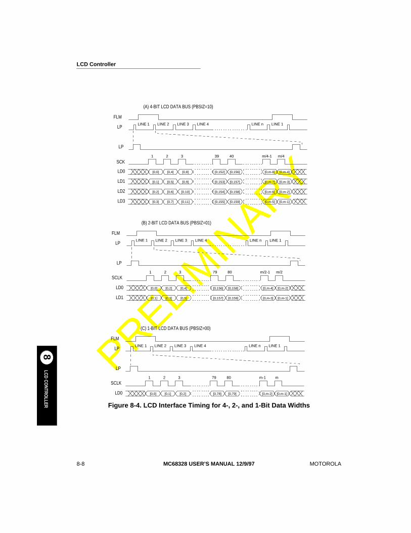
LCD Controller
8-8
MC68328 USER’S MANUAL 12/9/97
MOTOROLA
LCD CONTRO
LLER
8
PRELIM
INARY
Figure 8-4. LCD Interface Timing for 4-, 2-, and 1-Bit Data Widths
SCLK
LD0 [0,0] [0,2] [0,4]
LD1 [0,1] [0,3] [0,5]
LP
FLM
[0,m-4] [0,m-2]
[0,m-3] [0,m-1]
LP
LINE 1
[0,156] [0,158]
[0,157] [0,159]
LINE 2 LINE 3 LINE 4 LINE n LINE 1
1 2 3 m/2m/2-179 80
(B) 2-BIT LCD DATA BUS (PBSIZ=01)
LD0 [0,0] [0,4] [0,8]
LD1 [0,1] [0,5] [0,9]
LD2 [0,2] [0,6] [0,10]
LD3 [0,3] [0,7] [0,11]
[0,m-8] [0,m-4]
[0,m-7] [0,m-3]
[0,m-6] [0,m-2]
[0,m-5] [0,m-1]
[0,152] [0,156]
[0,153] [0,157]
[0,154] [0,158]
[0,155] [0,159]
SCK1 2 3 m/4m/4-139 40
LP
FLM
LP
LINE 1 LINE 2 LINE 3 LINE 4 LINE n LINE 1
(A) 4-BIT LCD DATA BUS (PBSIZ=10)
SCLK
LD0 [0,0] [0,1] [0,2]
LP
FLM
[0,m-2] [0,m-1]
LP
LINE 1
[0,78] [0,79]
LINE 2 LINE 3 LINE 4 LINE n LINE 1
1 2 3 m m-179 80
(C) 1-BIT LCD DATA BUS (PBSIZ=00)
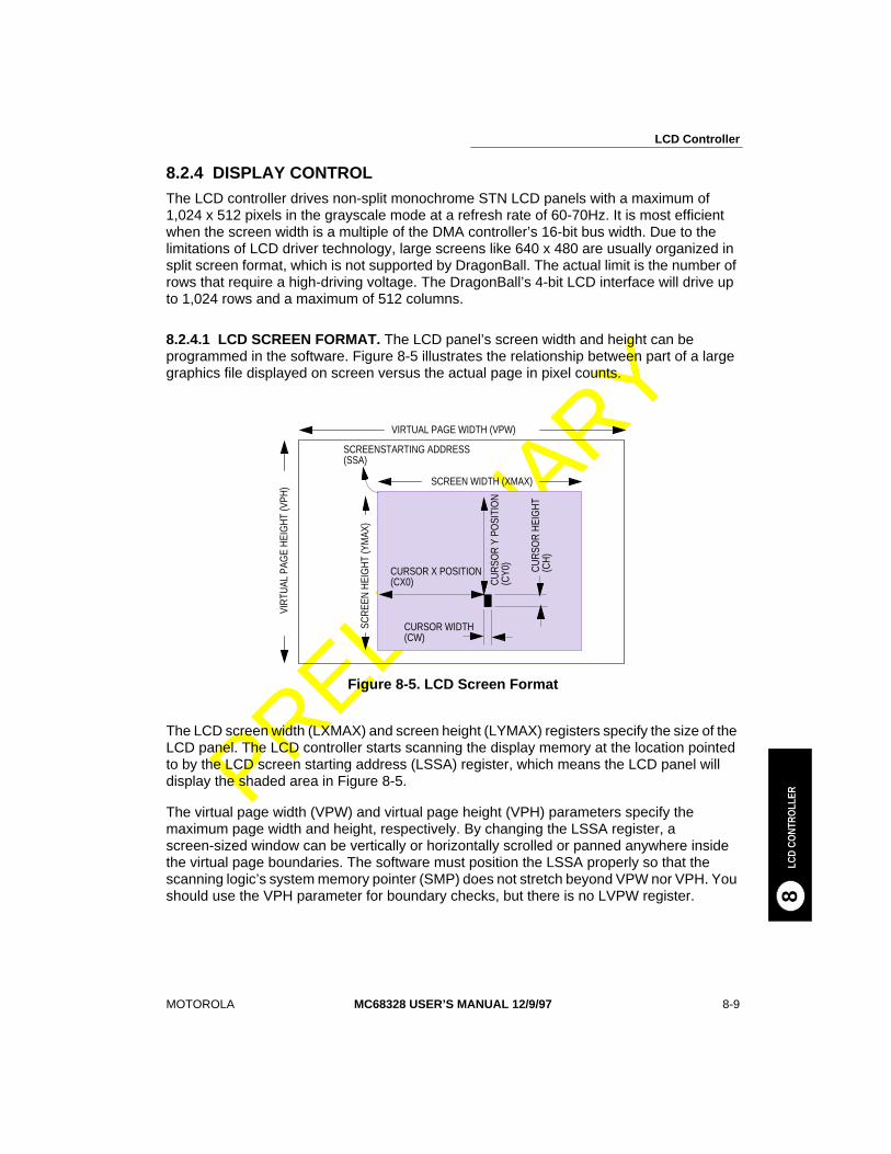
LCD Controller
MOTOROLA
MC68328 USER’S MANUAL 12/9/97
8-9
LCD
CONT
ROLL
ER
8
PRELIM
INARY
8.2.4 DISPLAY CONTROL
The LCD controller drives non-split monochrome STN LCD panels with a maximum of 1,024 x 512 pixels in the grayscale mode at a refresh rate of 60-70Hz. It is most efficient when the screen width is a multiple of the DMA controller’s 16-bit bus width. Due to the limitations of LCD driver technology, large screens like 640 x 480 are usually organized in split screen format, which is not supported by DragonBall. The actual limit is the number of rows that require a high-driving voltage. The DragonBall’s 4-bit LCD interface will drive up to 1,024 rows and a maximum of 512 columns.
8.2.4.1 LCD SCREEN FORMAT.
The LCD panel’s screen width and height can be programmed in the software. Figure 8-5 illustrates the relationship between part of a large graphics file displayed on screen versus the actual page in pixel counts.
The LCD screen width (LXMAX) and screen height (LYMAX) registers specify the size of the LCD panel. The LCD controller starts scanning the display memory at the location pointed to by the LCD screen starting address (LSSA) register, which means the LCD panel will display the shaded area in Figure 8-5.
The virtual page width (VPW) and virtual page height (VPH) parameters specify the maximum page width and height, respectively. By changing the LSSA register, a screen-sized window can be vertically or horizontally scrolled or panned anywhere inside the virtual page boundaries. The software must position the LSSA properly so that the scanning logic’s system memory pointer (SMP) does not stretch beyond VPW nor VPH. You should use the VPH parameter for boundary checks, but there is no LVPW register.
Figure 8-5. LCD Screen Format
SCREEN WIDTH (XMAX)
VIRTUAL PAGE WIDTH (VPW)
SCREENSTARTING ADDRESS (SSA)
VIR
TUAL
PAG
E H
EIG
HT
(VPH
)
CURSOR X POSITION
CU
RSO
R Y
PO
SITI
ON
(CX0) (CY0
)
CURSOR WIDTH(CW)
CU
RSO
R H
EIG
HT
(CH
)
SCR
EEN
HEI
GH
T (Y
MAX
)
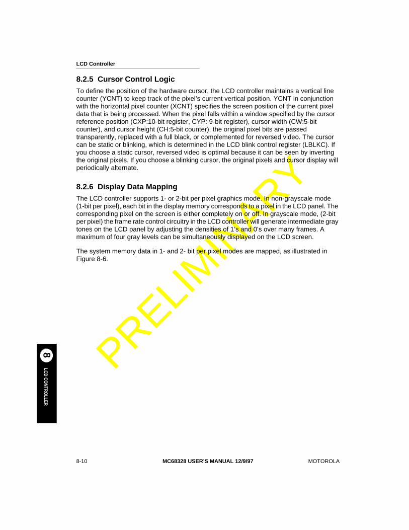
LCD Controller
8-10
MC68328 USER’S MANUAL 12/9/97
MOTOROLA
LCD CONTRO
LLER
8
PRELIM
INARY
8.2.5 Cursor Control Logic
To define the position of the hardware cursor, the LCD controller maintains a vertical line counter (YCNT) to keep track of the pixel’s current vertical position. YCNT in conjunction with the horizontal pixel counter (XCNT) specifies the screen position of the current pixel data that is being processed. When the pixel falls within a window specified by the cursor reference position (CXP:10-bit register, CYP: 9-bit register), cursor width (CW:5-bit counter), and cursor height (CH:5-bit counter), the original pixel bits are passed transparently, replaced with a full black, or complemented for reversed video. The cursor can be static or blinking, which is determined in the LCD blink control register (LBLKC). If you choose a static cursor, reversed video is optimal because it can be seen by inverting the original pixels. If you choose a blinking cursor, the original pixels and cursor display will periodically alternate.
8.2.6 Display Data Mapping
The LCD controller supports 1- or 2-bit per pixel graphics mode. In non-grayscale mode (1-bit per pixel), each bit in the display memory corresponds to a pixel in the LCD panel. The corresponding pixel on the screen is either completely on or off. In grayscale mode, (2-bit per pixel) the frame rate control circuitry in the LCD controller will generate intermediate gray tones on the LCD panel by adjusting the densities of 1’s and 0’s over many frames. A maximum of four gray levels can be simultaneously displayed on the LCD screen.
The system memory data in 1- and 2- bit per pixel modes are mapped, as illustrated in Figure 8-6.
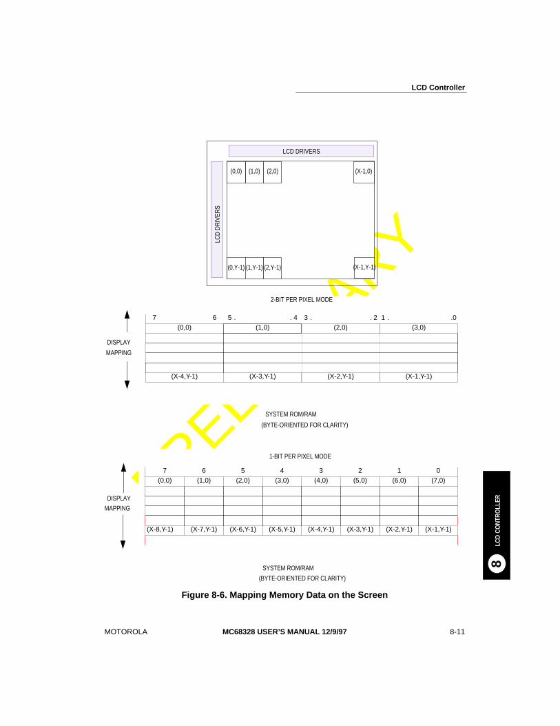
LCD Controller
MOTOROLA
MC68328 USER’S MANUAL 12/9/97
8-11
LCD
CONT
ROLL
ER
8
PRELIM
INARY
Figure 8-6. Mapping Memory Data on the Screen
7 6 5 4 3 2 1 0(0,0) (1,0) (2,0) (3,0) (4,0) (5,0) (6,0) (7,0)
(X-8,Y-1) (X-7,Y-1) (X-6,Y-1) (X-5,Y-1) (X-4,Y-1) (X-3,Y-1) (X-2,Y-1) (X-1,Y-1)
1-BIT PER PIXEL MODE
(BYTE-ORIENTED FOR CLARITY)
LCD DRIVERS
LCD
DR
IVER
S
(1,0) (2,0) (X-1,0)(0,0)
(0,Y-1) (1,Y-1) (2,Y-1) (X-1,Y-1)
(BYTE-ORIENTED FOR CLARITY)
SYSTEM ROM/RAM
SYSTEM ROM/RAM
DISPLAY
MAPPING
2-BIT PER PIXEL MODE
7 .............................6 5 . . . . . . . . . . . . . . . . 4 3 . . . . . . . . . . . . . . . . . 2 1 . . . . . . . . . . . . . . . . . .0(0,0) (1,0) (2,0) (3,0)
(X-4,Y-1) (X-3,Y-1) (X-2,Y-1) (X-1,Y-1)
DISPLAY
MAPPING
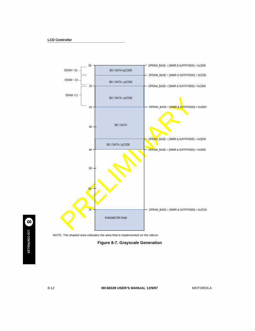
LCD Controller
8-12 MC68328 USER’S MANUAL 12/9/97 MOTOROLA
LCD CONTRO
LLER8 PRELI
MIN
ARY
Figure 8-7. Grayscale Generation
BD / DATA /µCODE
BD / DATA / µCODE
0K
6K
PARAMETER RAM
BD / DATA
ERAM = 10
BD / DATA / µCODE
7K
BD / DATA / µCODE
DPRAM_BASE = (IMMR & 0xFFFF0000) + 0x2000
DPRAM_BASE = (IMMR & 0xFFFF0000) + 0x2400
DPRAM_BASE = (IMMR & 0xFFFF0000) + 0x2800
DPRAM_BASE = (IMMR & 0xFFFF0000) + 0x3000
DPRAM_BASE = (IMMR & 0xFFFF0000) + 0x3C00
DPRAM_BASE = (IMMR & 0xFFFF0000) + 0x2200
DPRAM_BASE = (IMMR & 0xFFFF0000) + 0x2E00
ERAM = 01
3K
ERAM =11
4K
5K
2K
1K
NOTE: The shaded area indicates the area that is implemented on the silicon.
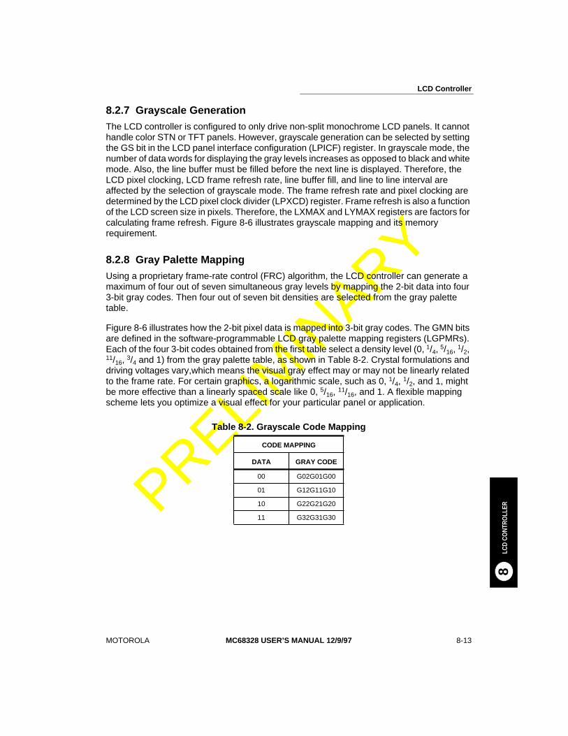
LCD Controller
MOTOROLA MC68328 USER’S MANUAL 12/9/97 8-13
LCD
CONT
ROLL
ER8PRELI
MIN
ARY
8.2.7 Grayscale GenerationThe LCD controller is configured to only drive non-split monochrome LCD panels. It cannot handle color STN or TFT panels. However, grayscale generation can be selected by setting the GS bit in the LCD panel interface configuration (LPICF) register. In grayscale mode, the number of data words for displaying the gray levels increases as opposed to black and white mode. Also, the line buffer must be filled before the next line is displayed. Therefore, the LCD pixel clocking, LCD frame refresh rate, line buffer fill, and line to line interval are affected by the selection of grayscale mode. The frame refresh rate and pixel clocking are determined by the LCD pixel clock divider (LPXCD) register. Frame refresh is also a function of the LCD screen size in pixels. Therefore, the LXMAX and LYMAX registers are factors for calculating frame refresh. Figure 8-6 illustrates grayscale mapping and its memory requirement.
8.2.8 Gray Palette MappingUsing a proprietary frame-rate control (FRC) algorithm, the LCD controller can generate a maximum of four out of seven simultaneous gray levels by mapping the 2-bit data into four 3-bit gray codes. Then four out of seven bit densities are selected from the gray palette table.
Figure 8-6 illustrates how the 2-bit pixel data is mapped into 3-bit gray codes. The GMN bits are defined in the software-programmable LCD gray palette mapping registers (LGPMRs). Each of the four 3-bit codes obtained from the first table select a density level (0, 1/4, 5/16, 1/2, 11/16, 3/4 and 1) from the gray palette table, as shown in Table 8-2. Crystal formulations and driving voltages vary,which means the visual gray effect may or may not be linearly related to the frame rate. For certain graphics, a logarithmic scale, such as 0, 1/4, 1/2, and 1, might be more effective than a linearly spaced scale like 0, 5/16, 11/16, and 1. A flexible mapping scheme lets you optimize a visual effect for your particular panel or application.
Table 8-2. Grayscale Code Mapping
CODE MAPPING
DATA GRAY CODE
00 G02G01G00
01 G12G11G10
10 G22G21G20
11 G32G31G30
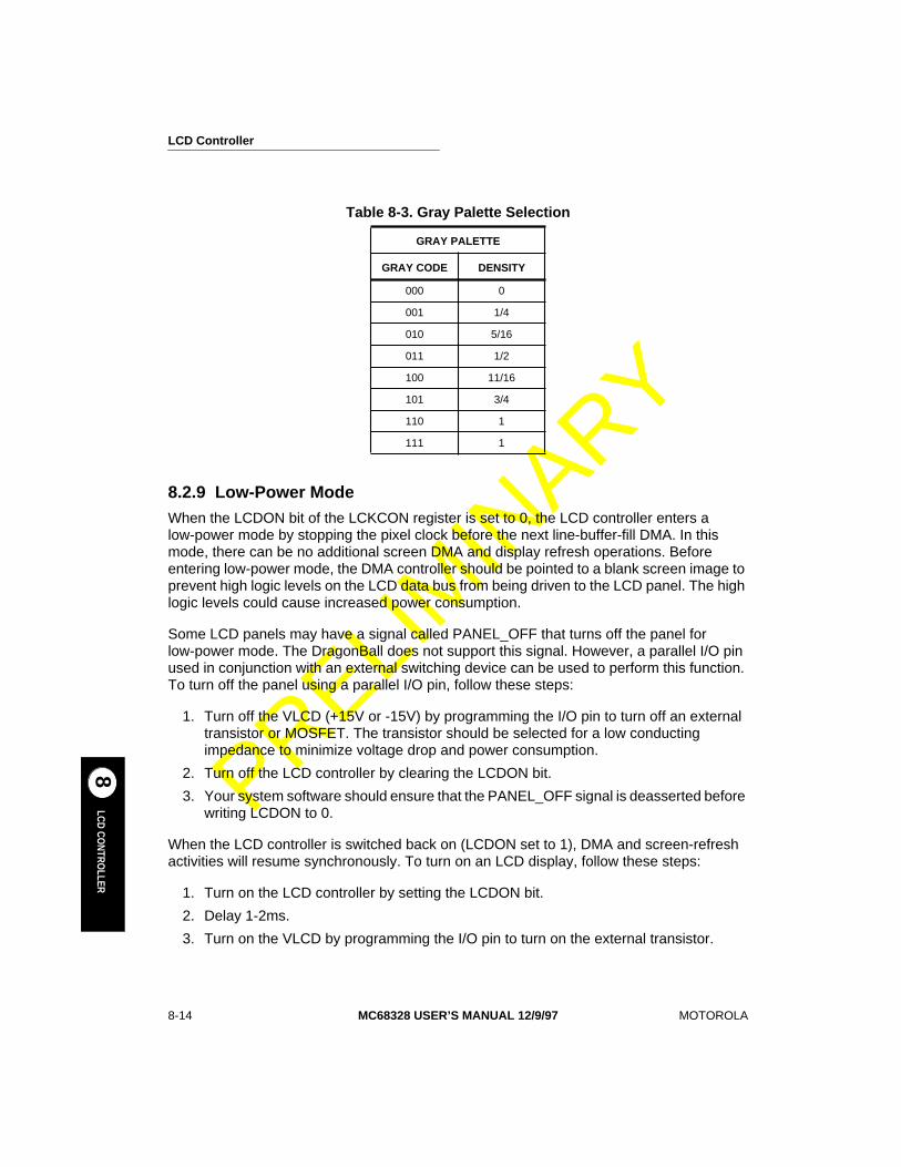
LCD Controller
8-14 MC68328 USER’S MANUAL 12/9/97 MOTOROLA
LCD CONTRO
LLER8 PRELI
MIN
ARY8.2.9 Low-Power ModeWhen the LCDON bit of the LCKCON register is set to 0, the LCD controller enters a low-power mode by stopping the pixel clock before the next line-buffer-fill DMA. In this mode, there can be no additional screen DMA and display refresh operations. Before entering low-power mode, the DMA controller should be pointed to a blank screen image to prevent high logic levels on the LCD data bus from being driven to the LCD panel. The high logic levels could cause increased power consumption.
Some LCD panels may have a signal called PANEL_OFF that turns off the panel for low-power mode. The DragonBall does not support this signal. However, a parallel I/O pin used in conjunction with an external switching device can be used to perform this function. To turn off the panel using a parallel I/O pin, follow these steps:
1. Turn off the VLCD (+15V or -15V) by programming the I/O pin to turn off an external transistor or MOSFET. The transistor should be selected for a low conducting impedance to minimize voltage drop and power consumption.
2. Turn off the LCD controller by clearing the LCDON bit.
3. Your system software should ensure that the PANEL_OFF signal is deasserted before writing LCDON to 0.
When the LCD controller is switched back on (LCDON set to 1), DMA and screen-refresh activities will resume synchronously. To turn on an LCD display, follow these steps:
1. Turn on the LCD controller by setting the LCDON bit.
2. Delay 1-2ms.
3. Turn on the VLCD by programming the I/O pin to turn on the external transistor.
Table 8-3. Gray Palette Selection
GRAY PALETTE
GRAY CODE DENSITY
000 0
001 1/4
010 5/16
011 1/2
100 11/16
101 3/4
110 1
111 1
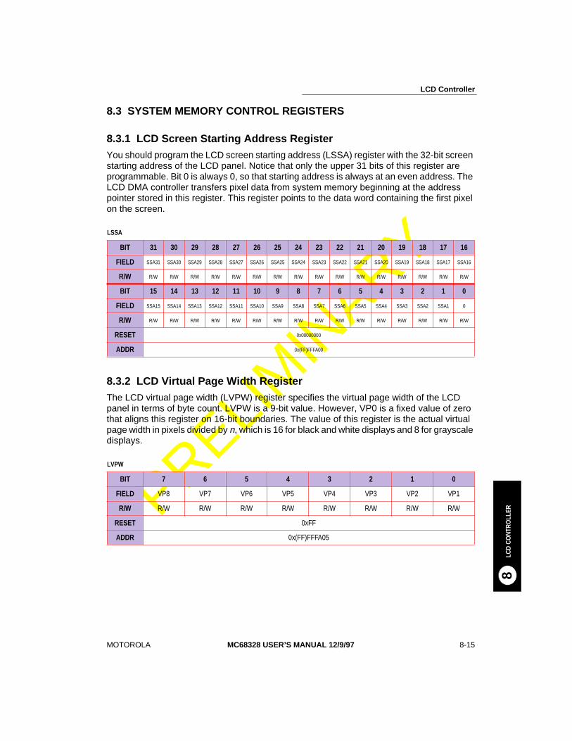
LCD Controller
MOTOROLA MC68328 USER’S MANUAL 12/9/97 8-15
LCD
CONT
ROLL
ER8PRELI
MIN
ARY
8.3 SYSTEM MEMORY CONTROL REGISTERS
8.3.1 LCD Screen Starting Address RegisterYou should program the LCD screen starting address (LSSA) register with the 32-bit screen starting address of the LCD panel. Notice that only the upper 31 bits of this register are programmable. Bit 0 is always 0, so that starting address is always at an even address. The LCD DMA controller transfers pixel data from system memory beginning at the address pointer stored in this register. This register points to the data word containing the first pixel on the screen.
8.3.2 LCD Virtual Page Width RegisterThe LCD virtual page width (LVPW) register specifies the virtual page width of the LCD panel in terms of byte count. LVPW is a 9-bit value. However, VP0 is a fixed value of zero that aligns this register on 16-bit boundaries. The value of this register is the actual virtual page width in pixels divided by n, which is 16 for black and white displays and 8 for grayscale displays.
LSSA
BIT 31 30 29 28 27 26 25 24 23 22 21 20 19 18 17 16
FIELD SSA31 SSA30 SSA29 SSA28 SSA27 SSA26 SSA25 SSA24 SSA23 SSA22 SSA21 SSA20 SSA19 SSA18 SSA17 SSA16
R/W R/W R/W R/W R/W R/W R/W R/W R/W R/W R/W R/W R/W R/W R/W R/W R/W
BIT 15 14 13 12 11 10 9 8 7 6 5 4 3 2 1 0
FIELD SSA15 SSA14 SSA13 SSA12 SSA11 SSA10 SSA9 SSA8 SSA7 SSA6 SSA5 SSA4 SSA3 SSA2 SSA1 0
R/W R/W R/W R/W R/W R/W R/W R/W R/W R/W R/W R/W R/W R/W R/W R/W R/W
RESET 0x00000000
ADDR 0x(FF)FFFA00
LVPW
BIT 7 6 5 4 3 2 1 0
FIELD VP8 VP7 VP6 VP5 VP4 VP3 VP2 VP1
R/W R/W R/W R/W R/W R/W R/W R/W R/W
RESET 0xFF
ADDR 0x(FF)FFFA05
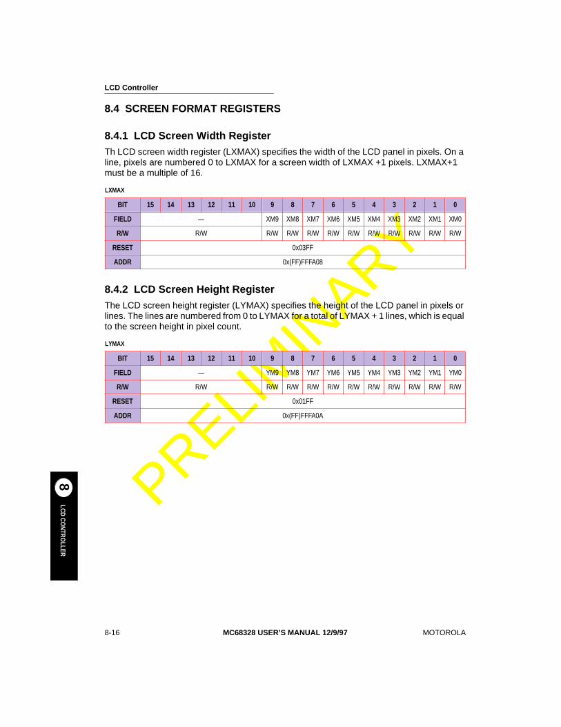
LCD Controller
8-16 MC68328 USER’S MANUAL 12/9/97 MOTOROLA
LCD CONTRO
LLER8 PRELI
MIN
ARY
8.4 SCREEN FORMAT REGISTERS
8.4.1 LCD Screen Width RegisterTh LCD screen width register (LXMAX) specifies the width of the LCD panel in pixels. On a line, pixels are numbered 0 to LXMAX for a screen width of LXMAX +1 pixels. LXMAX+1 must be a multiple of 16.
8.4.2 LCD Screen Height RegisterThe LCD screen height register (LYMAX) specifies the height of the LCD panel in pixels or lines. The lines are numbered from 0 to LYMAX for a total of LYMAX + 1 lines, which is equal to the screen height in pixel count.
LXMAX
BIT 15 14 13 12 11 10 9 8 7 6 5 4 3 2 1 0
FIELD — XM9 XM8 XM7 XM6 XM5 XM4 XM3 XM2 XM1 XM0
R/W R/W R/W R/W R/W R/W R/W R/W R/W R/W R/W R/W
RESET 0x03FF
ADDR 0x(FF)FFFA08
LYMAX
BIT 15 14 13 12 11 10 9 8 7 6 5 4 3 2 1 0
FIELD — YM9 YM8 YM7 YM6 YM5 YM4 YM3 YM2 YM1 YM0
R/W R/W R/W R/W R/W R/W R/W R/W R/W R/W R/W R/W
RESET 0x01FF
ADDR 0x(FF)FFFA0A
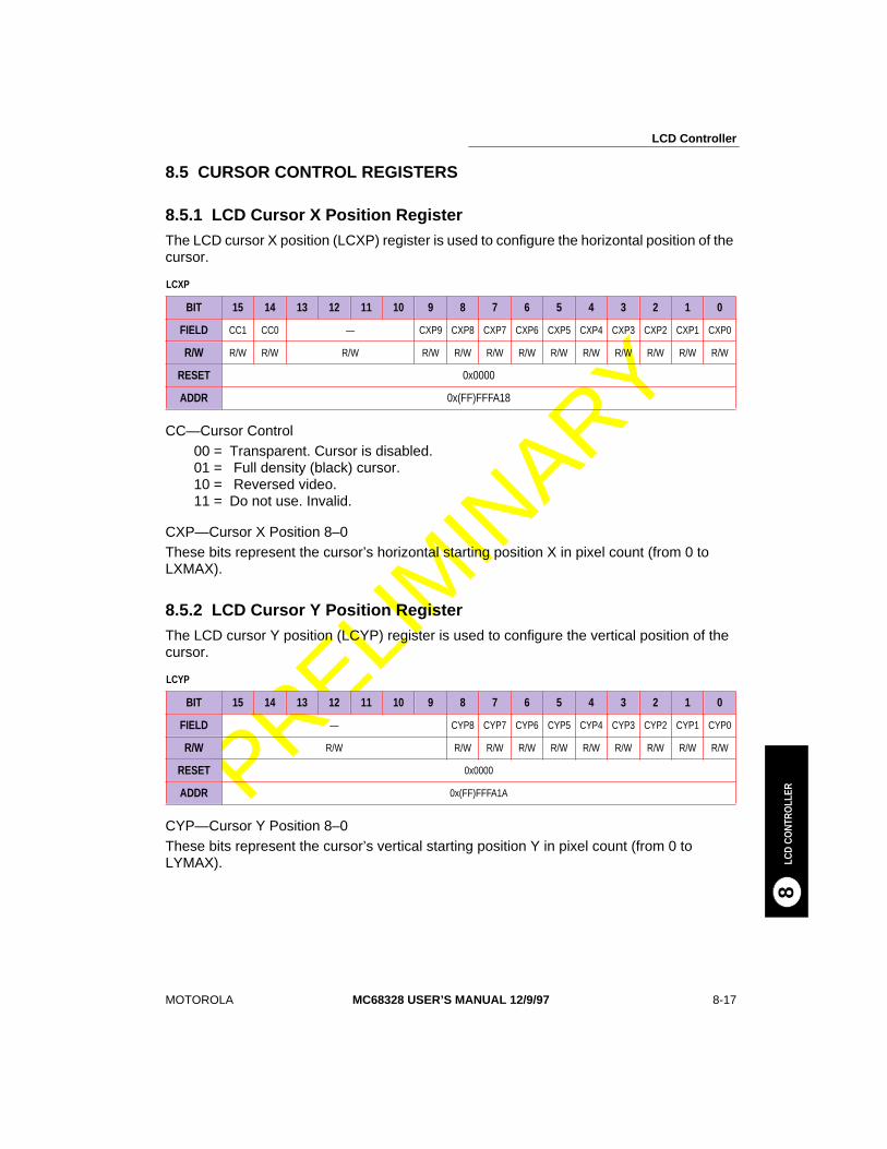
LCD Controller
MOTOROLA MC68328 USER’S MANUAL 12/9/97 8-17
LCD
CONT
ROLL
ER8PRELI
MIN
ARY
8.5 CURSOR CONTROL REGISTERS
8.5.1 LCD Cursor X Position RegisterThe LCD cursor X position (LCXP) register is used to configure the horizontal position of the cursor.
CC—Cursor Control00 = Transparent. Cursor is disabled.01 = Full density (black) cursor.10 = Reversed video.11 = Do not use. Invalid.
CXP—Cursor X Position 8–0These bits represent the cursor’s horizontal starting position X in pixel count (from 0 to LXMAX).
8.5.2 LCD Cursor Y Position RegisterThe LCD cursor Y position (LCYP) register is used to configure the vertical position of the cursor.
CYP—Cursor Y Position 8–0These bits represent the cursor’s vertical starting position Y in pixel count (from 0 to LYMAX).
LCXP
BIT 15 14 13 12 11 10 9 8 7 6 5 4 3 2 1 0
FIELD CC1 CC0 — CXP9 CXP8 CXP7 CXP6 CXP5 CXP4 CXP3 CXP2 CXP1 CXP0
R/W R/W R/W R/W R/W R/W R/W R/W R/W R/W R/W R/W R/W R/W
RESET 0x0000
ADDR 0x(FF)FFFA18
LCYP
BIT 15 14 13 12 11 10 9 8 7 6 5 4 3 2 1 0
FIELD — CYP8 CYP7 CYP6 CYP5 CYP4 CYP3 CYP2 CYP1 CYP0
R/W R/W R/W R/W R/W R/W R/W R/W R/W R/W R/W
RESET 0x0000
ADDR 0x(FF)FFFA1A
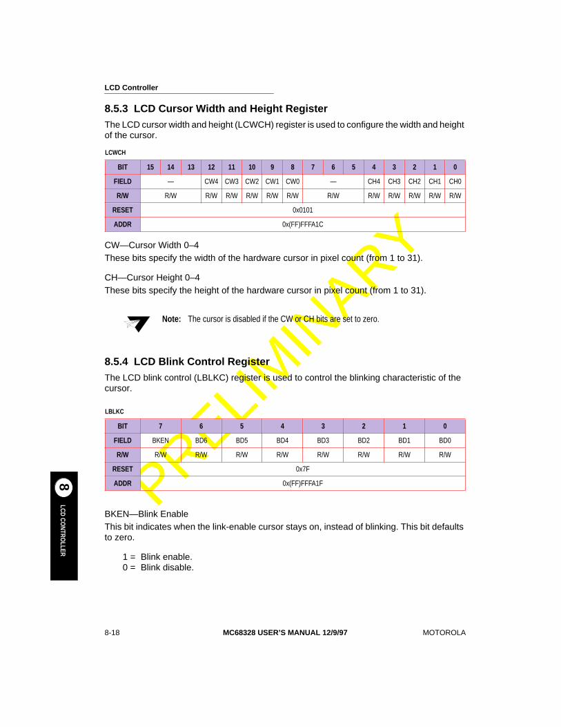
LCD Controller
8-18 MC68328 USER’S MANUAL 12/9/97 MOTOROLA
LCD CONTRO
LLER8 PRELI
MIN
ARY
8.5.3 LCD Cursor Width and Height RegisterThe LCD cursor width and height (LCWCH) register is used to configure the width and height of the cursor.
CW—Cursor Width 0–4These bits specify the width of the hardware cursor in pixel count (from 1 to 31).
CH—Cursor Height 0–4These bits specify the height of the hardware cursor in pixel count (from 1 to 31).
8.5.4 LCD Blink Control RegisterThe LCD blink control (LBLKC) register is used to control the blinking characteristic of the cursor.
BKEN—Blink EnableThis bit indicates when the link-enable cursor stays on, instead of blinking. This bit defaults to zero.
1 = Blink enable.0 = Blink disable.
LCWCH
BIT 15 14 13 12 11 10 9 8 7 6 5 4 3 2 1 0
FIELD — CW4 CW3 CW2 CW1 CW0 — CH4 CH3 CH2 CH1 CH0
R/W R/W R/W R/W R/W R/W R/W R/W R/W R/W R/W R/W R/W
RESET 0x0101
ADDR 0x(FF)FFFA1C
Note: The cursor is disabled if the CW or CH bits are set to zero.
LBLKC
BIT 7 6 5 4 3 2 1 0
FIELD BKEN BD6 BD5 BD4 BD3 BD2 BD1 BD0
R/W R/W R/W R/W R/W R/W R/W R/W R/W
RESET 0x7F
ADDR 0x(FF)FFFA1F
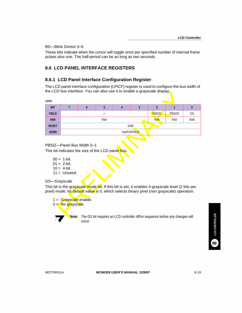
LCD Controller
MOTOROLA MC68328 USER’S MANUAL 12/9/97 8-19
LCD
CONT
ROLL
ER8PRELI
MIN
ARY
BD—Blink Divisor 0–6These bits indicate when the cursor will toggle once per specified number of internal frame pulses plus one. The half-period can be as long as two seconds.
8.6 LCD PANEL INTERFACE REGISTERS
8.6.1 LCD Panel Interface Configuration RegisterThe LCD panel interface configuration (LPICF) register is used to configure the bus width of the LCD bus interface. You can also use it to enable a grayscale display.
PBSIZ—Panel Bus Width 0–1This bit indicates the size of the LCD panel bus.
00 = 1-bit.01 = 2-bit.10 = 4-bit.11 = Unused.
GS—GrayscaleThis bit is the grayscale mode bit. If this bit is set, it enables 4-grayscale level (2 bits per pixel) mode. Its default value is 0, which selects binary pixel (non grayscale) operation.
1 = Grayscale enable.0 = No grayscale.
LPICF
BIT 7 6 5 4 3 2 1 0
FIELD — PBSIZ1 PBSIZ0 GS
R/W RW/ R/W R/W R/W
RESET 0x00
ADDR 0x(FF)FFFA20
Note: The GS bit requires an LCD controller off/on sequence before any changes willoccur.
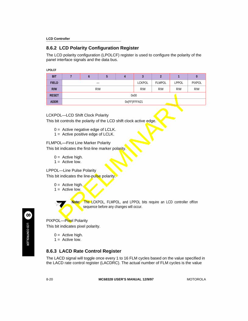
LCD Controller
8-20 MC68328 USER’S MANUAL 12/9/97 MOTOROLA
LCD CONTRO
LLER8 PRELI
MIN
ARY
8.6.2 LCD Polarity Configuration RegisterThe LCD polarity configuration (LPOLCF) register is used to configure the polarity of the panel interface signals and the data bus.
LCKPOL—LCD Shift Clock PolarityThis bit controls the polarity of the LCD shift clock active edge.
0 = Active negative edge of LCLK.1 = Active positive edge of LCLK.
FLMPOL—First Line Marker PolarityThis bit indicates the first-line marker polarity.
0 = Active high.1 = Active low.
LPPOL—Line Pulse PolarityThis bit indicates the line-pulse polarity.
0 = Active high.1 = Active low.
PIXPOL—Pixel PolarityThis bit indicates pixel polarity.
0 = Active high.1 = Active low.
8.6.3 LACD Rate Control RegisterThe LACD signal will toggle once every 1 to 16 FLM cycles based on the value specified in the LACD rate control register (LACDRC). The actual number of FLM cycles is the value
LPOLCF
BIT 7 6 5 4 3 2 1 0
FIELD — LCKPOL FLMPOL LPPOL PIXPOL
R/W R/W R/W R/W R/W R/W
RESET 0x00
ADDR 0x(FF)FFFA21
Note: The LCKPOL, FLMPOL, and LPPOL bits require an LCD controller off/onsequence before any changes will occur.
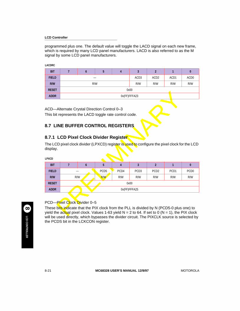
LCD Controller
8-21 MC68328 USER’S MANUAL 12/9/97 MOTOROLA
LCD CONTRO
LLER8 PRELI
MIN
ARY
programmed plus one. The default value will toggle the LACD signal on each new frame, which is required by many LCD panel manufacturers. LACD is also referred to as the M signal by some LCD panel manufacturers.
ACD—Alternate Crystal Direction Control 0–3This bit represents the LACD toggle rate control code.
8.7 LINE BUFFER CONTROL REGISTERS
8.7.1 LCD Pixel Clock Divider RegisterThe LCD pixel clock divider (LPXCD) register is used to configure the pixel clock for the LCD display.
PCD—Pixel Clock Divider 0–5These bits indicate that the PIX clock from the PLL is divided by N (PCD5-0 plus one) to yield the actual pixel clock. Values 1-63 yield N = 2 to 64. If set to 0 (N = 1), the PIX clock will be used directly, which bypasses the divider circuit. The PIXCLK source is selected by the PCDS bit in the LCKCON register.
LACDRC
BIT 7 6 5 4 3 2 1 0
FIELD — ACD3 ACD2 ACD1 ACD0
R/W R/W R/W R/W R/W R/W
RESET 0x00
ADDR 0x(FF)FFFA23
LPXCD
BIT 7 6 5 4 3 2 1 0
FIELD — PCD5 PCD4 PCD3 PCD2 PCD1 PCD0
R/W R/W R/W R/W R/W R/W R/W R/W
RESET 0x00
ADDR 0x(FF)FFFA25
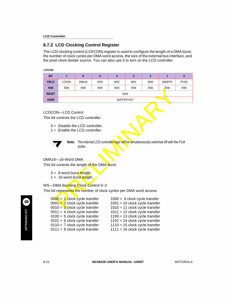
LCD Controller
8-22 MC68328 USER’S MANUAL 12/9/97 MOTOROLA
LCD CONTRO
LLER8 PRELI
MIN
ARY
8.7.2 LCD Clocking Control RegisterThe LCD clocking control (LCKCON) register is used to configure the length of a DMA burst, the number of clock cycles per DMA word access, the size of the external bus interface, and the pixel clock divider source. You can also use it to turn on the LCD controller.
LCDCON—LCD ControlThis bit controls the LCD controller.
0 = Disable the LCD controller.1 = Enable the LCD controller.
DMA16—16-Word DMAThis bit controls the length of the DMA burst.
0 = 8-word burst length.1 = 16-word burst length.
WS—DMA Bursting Clock Control 0–3This bit represents the number of clock cycles per DMA word access.
0000 = 1 clock cycle transfer 1000 = 9 clock cycle transfer0001 = 2 clock cycle transfer 1001 = 10 clock cycle transfer0010 = 3 clock cycle transfer 1010 = 11 clock cycle transfer0011 = 4 clock cycle transfer 1011 = 12 clock cycle transfer0100 = 5 clock cycle transfer 1100 = 13 clock cycle transfer0101 = 6 clock cycle transfer 1101 = 14 clock cycle transfer0110 = 7 clock cycle transfer 1110 = 15 clock cycle transfer0111 = 8 clock cycle transfer 1111 = 16 clock cycle transfer
LCKCON
BIT 7 6 5 4 3 2 1 0
FIELD LCDON DMA16 WS3 WS2 WS1 WS0 DWIDTH PCDS
R/W R/W R/W R/W R/W R/W R/W R/W R/W
RESET 0x40
ADDR 0x(FF)FFFA27
Note: The internal LCD controller logic will be simultaneously switched off with the FLMpulse.
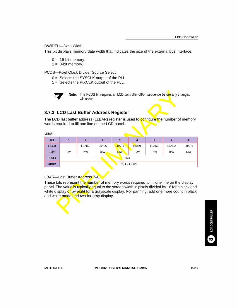
LCD Controller
MOTOROLA MC68328 USER’S MANUAL 12/9/97 8-23
LCD
CONT
ROLL
ER8PRELI
MIN
ARY
DWIDTH—Data WidthThis bit displays memory data width that indicates the size of the external bus interface.
0 = 16-bit memory.1 = 8-bit memory.
PCDS—Pixel Clock Divider Source Select0 = Selects the SYSCLK output of the PLL.1 = Selects the PIXCLK output of the PLL.
8.7.3 LCD Last Buffer Address RegisterThe LCD last buffer address (LLBAR) register is used to configure the number of memory words required to fill one line on the LCD panel.
LBAR—Last Buffer Address 7–0These bits represent the number of memory words required to fill one line on the display panel. The value is typically equal to the screen width in pixels divided by 16 for a black and white display or by eight for a grayscale display. For panning, add one more count in black and white mode and two for gray display.
Note: The PCDS bit requires an LCD controller off/on sequence before any changeswill occur.
LLBAR
BIT 7 6 5 4 3 2 1 0
FIELD — LBAR7 LBAR6 LBAR5 LBAR4 LBAR3 LBAR2 LBAR1
R/W R/W R/W R/W R/W R/W R/W R/W R/W
RESET 0x3E
ADDR 0x(FF)FFFA29
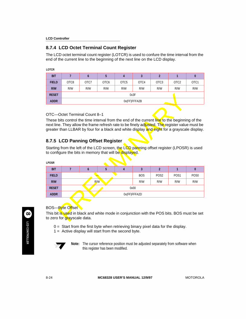
LCD Controller
8-24 MC68328 USER’S MANUAL 12/9/97 MOTOROLA
LCD CONTRO
LLER8 PRELI
MIN
ARY
8.7.4 LCD Octet Terminal Count RegisterThe LCD octet terminal count register (LOTCR) is used to confure the time interval from the end of the current line to the beginning of the next line on the LCD display.
OTC—Octet Terminal Count 8–1These bits control the time interval from the end of the current line to the beginning of the next line. They allow the frame refresh rate to be finely adjusted. The register value must be greater than LLBAR by four for a black and white display and eight for a grayscale display.
8.7.5 LCD Panning Offset RegisterStarting from the left of the LCD screen, the LCD panning offset register (LPOSR) is used to configure the bits in memory that will be displayed.
BOS—Byte OffsetThis bit is used in black and white mode in conjunction with the POS bits. BOS must be set to zero for grayscale data.
0 = Start from the first byte when retrieving binary pixel data for the display.1 = Active display will start from the second byte.
LOTCR
BIT 7 6 5 4 3 2 1 0
FIELD OTC8 OTC7 OTC6 OTC5 OTC4 OTC3 OTC2 OTC1
R/W R/W R/W R/W R/W R/W R/W R/W R/W
RESET 0x3F
ADDR 0x(FF)FFFA2B
LPOSR
BIT 7 6 5 4 3 2 1 0
FIELD — BOS POS2 POS1 POS0
R/W R/W R/W R/W R/W R/W
RESET 0x00
ADDR 0x(FF)FFFA2D
Note: The cursor reference position must be adjusted separately from software whenthis register has been modified.
LCD Controller
MOTOROLA MC68328 USER’S MANUAL 12/9/97 8-25
LCD
CONT
ROLL
ER8PRELI
MIN
ARY
POS—Pixel Offset Code 0–2These bits specify which of the eight pixels in the first or second (GS = 0, BOS = 1 only) octet retrieved from the line buffer is the first to be displayed on the screen. 000 implies that pixel 7, the first shifted out, will be the first to be displayed on every horizontal line in the current frame.
8.8 GRAYSCALE CONTROL REGISTERS
8.8.1 LCD Frame-Rate Modulation Control RegisterThe LCD frame rate modulation control (LFRCM) register contains default values that will give you satisfactory results when used with most LCD panels. However, if you do add a value, it should be odd and not even.
XMODX and YMODX—Frame-Rate Modulation ControlThese bits modulate adjacent pixels at different time periods to avoid spatial flicker or jitter when using frame-rate control. These values must be optimized by manually fine-tuning the targeted LCD panel. See Section 8.2.8 Gray Palette Mapping for details.
8.8.2 LCD Gray Palette Mapping RegisterThe LCD gray palette mapping register (LGPMR) is used to map the 2-bit grayscale value to its gray palette code.
GLEVELx—Grayscale Level 0–3These bits represent the gray palette code (bit position n=0, 1, 2) output for pixel-input data m (0 for pixel data 00, 1=01, 2=10, 3=11). This 3-bit code will then select one of seven bitstreams of different densities. See Section 8.2.8 Gray Palette Mapping for details.
LFRCM
BIT 7 6 5 4 3 2 1 0
FIELD XMOD3-XMOD0 YMOD3-YMOD0
R/W R/W R/W
RESET 0xB9
ADDR 0x(FF)FFFA31
LGPMR
BIT 15 14 13 12 11 10 9 8 7 6 5 4 3 2 1 0
FIELD GLEVEL1 GLEVEL0 GLEVEL2 GLEVEL3
R/W R/W R/W R/W R/W
RESET 0x0173
ADDR 0x(FF)FFFA32
LCD Controller
8-26 MC68328 USER’S MANUAL 12/9/97 MOTOROLA
LCD CONTRO
LLER8 PRELI
MIN
ARY
For example:
8.9 CALCULATING BANDWIDTHThe LCD’s DMA controller consumes bus bandwidth by periodically accessing memory. This is an important consideration for the high-performance handheld system designer.
8.9.1 Bus Overhead ConsiderationsThe following example describes the issues for estimating bandwidth overhead to the data bus. Consider a typical scenario:
Screen size: 320 x 240 pixels
Bits per pixel: 2 bits / pixel
Screen refresh rate: 60 Hz
System clock = 16.67 MHz
Host bus size: 16 bit
DMA access cycle: 2 cycles per 16-bit word
The period, Tl that the LCD controller must update one line of the screen is,
(EQ 1)
At the same time, the line buffer must be filled. The duration, TDMA, which the DMA cycle will take up the bus is,
(EQ 2)
2-BIT GRAYSCALE VALUE IN MEMORY
LEVEL LOG GRAY LEVEL
LINEAR GRAY LEVEL
(11) 3 111 (1) 111 (1)
(10) 2 011 (3/4) 100 (11/16)
(01) 1 001 (1/4) 010 (5/16)
(00) 0 000 (0) 000 (0)
Tl1
60Hz------------- 1
240lines--------------------×=
69.4µs=
TDMA320pixels 2bitperpixel× 2clock×
16.67MHz 16bitbus×---------------------------------------------------------------------------------------=
4.8µs=

LCD Controller
MOTOROLA MC68328 USER’S MANUAL 12/9/97 8-27
LCD
CONT
ROLL
ER8PRELI
MIN
ARY
Thus, the percentage of host bus time taken up by the LCDC DMA is PDMA,
(EQ 3)PDMA4.8`µs69.4 µ̀s-------------------=
6.92= %

LCD Controller
8-28 MC68328 USER’S MANUAL 12/9/97 MOTOROLA
LCD CONTRO
LLER8 PRELI
MIN
ARY
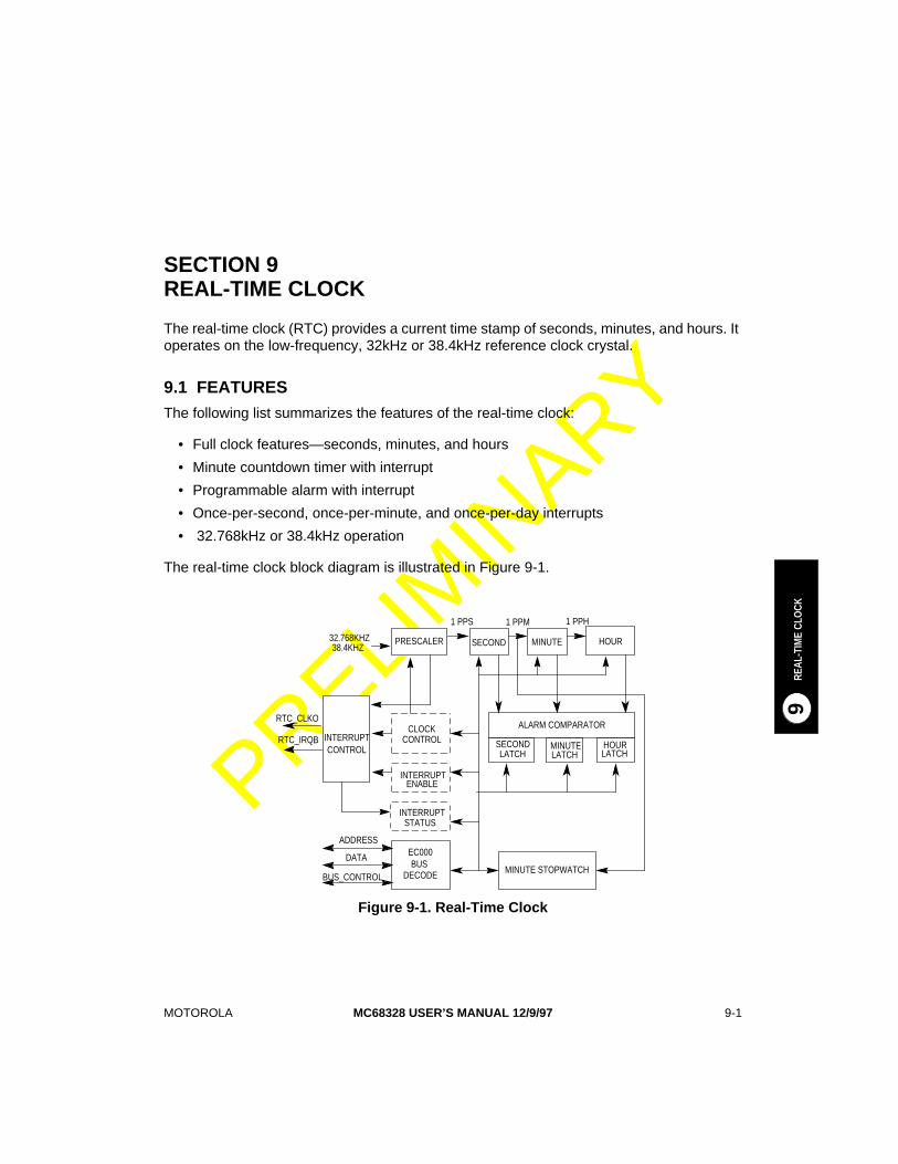
MOTOROLA
MC68328 USER’S MANUAL 12/9/97
9-1
REAL
-TIM
E CL
OCK
9
PRELIM
INARY
SECTION 9REAL-TIME CLOCK
The real-time clock (RTC) provides a current time stamp of seconds, minutes, and hours. It operates on the low-frequency, 32kHz or 38.4kHz reference clock crystal.
9.1 FEATURES
The following list summarizes the features of the real-time clock:
• Full clock features—seconds, minutes, and hours
• Minute countdown timer with interrupt
• Programmable alarm with interrupt
• Once-per-second, once-per-minute, and once-per-day interrupts
• 32.768kHz or 38.4kHz operation
The real-time clock block diagram is illustrated in Figure 9-1.
Figure 9-1. Real-Time Clock
PRESCALER SECOND MINUTE HOUR
ALARM COMPARATOR
SECONDLATCH
MINUTELATCH
HOURLATCH
CLOCKCONTROL
INTERRUPTENABLE
INTERRUPTSTATUS
MINUTE STOPWATCH
EC000BUS
DECODE
ADDRESS
DATA
BUS_CONTROL
32.768KHZ
RTC_IRQB INTERRUPTCONTROL
RTC_CLKO
38.4KHZ
1 PPS 1 PPM 1 PPH
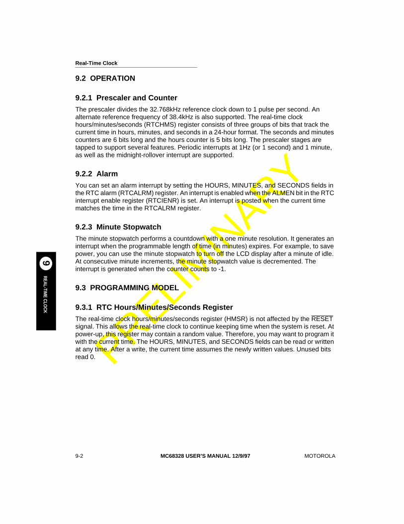
Real-Time Clock
9-2
MC68328 USER’S MANUAL 12/9/97
MOTOROLA
REAL-TIME CLO
CK
9
PRELIM
INARY
9.2 OPERATION
9.2.1 Prescaler and Counter
The prescaler divides the 32.768kHz reference clock down to 1 pulse per second. An alternate reference frequency of 38.4kHz is also supported. The real-time clock hours/minutes/seconds (RTCHMS) register consists of three groups of bits that track the current time in hours, minutes, and seconds in a 24-hour format. The seconds and minutes counters are 6 bits long and the hours counter is 5 bits long. The prescaler stages are tapped to support several features. Periodic interrupts at 1Hz (or 1 second) and 1 minute, as well as the midnight-rollover interrupt are supported.
9.2.2 Alarm
You can set an alarm interrupt by setting the HOURS, MINUTES, and SECONDS fields in the RTC alarm (RTCALRM) register. An interrupt is enabled when the ALMEN bit in the RTC interrupt enable register (RTCIENR) is set. An interrupt is posted when the current time matches the time in the RTCALRM register.
9.2.3 Minute Stopwatch
The minute stopwatch performs a countdown with a one minute resolution. It generates an interrupt when the programmable length of time (in minutes) expires. For example, to save power, you can use the minute stopwatch to turn off the LCD display after a minute of idle. At consecutive minute increments, the minute stopwatch value is decremented. The interrupt is generated when the counter counts to -1.
9.3 PROGRAMMING MODEL
9.3.1 RTC Hours/Minutes/Seconds Register
The real-time clock hours/minutes/seconds register (HMSR) is not affected by the RESET signal. This allows the real-time clock to continue keeping time when the system is reset. At power-up, this register may contain a random value. Therefore, you may want to program it with the current time. The HOURS, MINUTES, and SECONDS fields can be read or written at any time. After a write, the current time assumes the newly written values. Unused bits read 0.
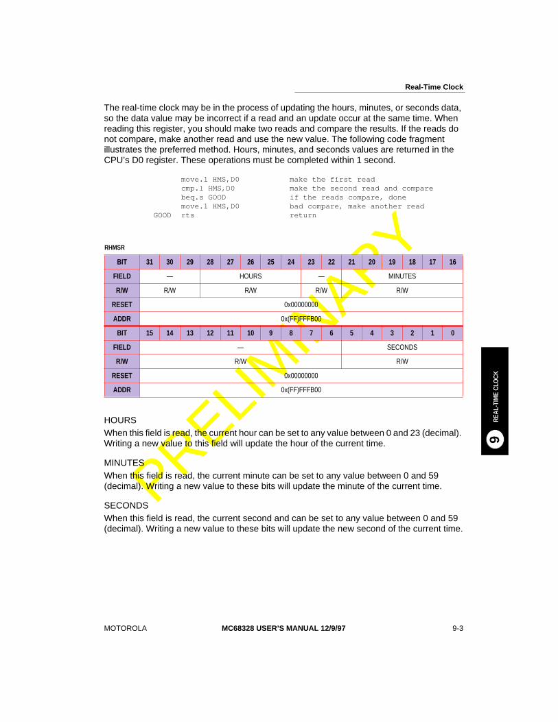
Real-Time Clock
MOTOROLA
MC68328 USER’S MANUAL 12/9/97
9-3
REAL
-TIM
E CL
OCK
9
PRELIM
INARY
The real-time clock may be in the process of updating the hours, minutes, or seconds data, so the data value may be incorrect if a read and an update occur at the same time. When reading this register, you should make two reads and compare the results. If the reads do not compare, make another read and use the new value. The following code fragment illustrates the preferred method. Hours, minutes, and seconds values are returned in the CPU’s D0 register. These operations must be completed within 1 second.
move.l HMS,D0 make the first readcmp.l HMS,D0 make the second read and comparebeq.s GOOD if the reads compare, donemove.l HMS,D0 bad compare, make another read
GOOD rts return
HOURSWhen this field is read, the current hour can be set to any value between 0 and 23 (decimal). Writing a new value to this field will update the hour of the current time.
MINUTESWhen this field is read, the current minute can be set to any value between 0 and 59 (decimal). Writing a new value to these bits will update the minute of the current time.
SECONDSWhen this field is read, the current second and can be set to any value between 0 and 59 (decimal). Writing a new value to these bits will update the new second of the current time.
RHMSR
BIT 31 30 29 28 27 26 25 24 23 22 21 20 19 18 17 16
FIELD
— HOURS — MINUTES
R/W
R/W R/W R/W R/W
RESET
0x00000000
ADDR
0x(FF)FFFB00
BIT 15 14 13 12 11 10 9 8 7 6 5 4 3 2 1 0
FIELD
— SECONDS
R/W
R/W R/W
RESET
0x00000000
ADDR
0x(FF)FFFB00
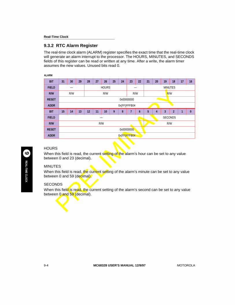
Real-Time Clock
9-4
MC68328 USER’S MANUAL 12/9/97
MOTOROLA
REAL-TIME CLO
CK
9
PRELIM
INARY
9.3.2 RTC Alarm Register
The real-time clock alarm (ALARM) register specifies the exact time that the real-time clock will generate an alarm interrupt to the processor. The HOURS, MINUTES, and SECONDS fields of this register can be read or written at any time. After a write, the alarm timer assumes the new values. Unused bits read 0.
HOURS When this field is read, the current setting of the alarm’s hour can be set to any value between 0 and 23 (decimal).
MINUTESWhen this field is read, the current setting of the alarm’s minute can be set to any value between 0 and 59 (decimal).
SECONDSWhen this field is read, the current setting of the alarm’s second can be set to any value between 0 and 59 (decimal).
ALARM
BIT 31 30 29 28 27 26 25 24 23 22 21 20 19 18 17 16
FIELD
— HOURS — MINUTES
R/W
R/W R/W R/W R/W
RESET
0x00000000
ADDR
0x(FF)FFFB04
BIT 15 14 13 12 11 10 9 8 7 6 5 4 3 2 1 0
FIELD
— SECONDS
R/W
R/W R/W
RESET
0x00000000
ADDR
0x(FF)FFFB04
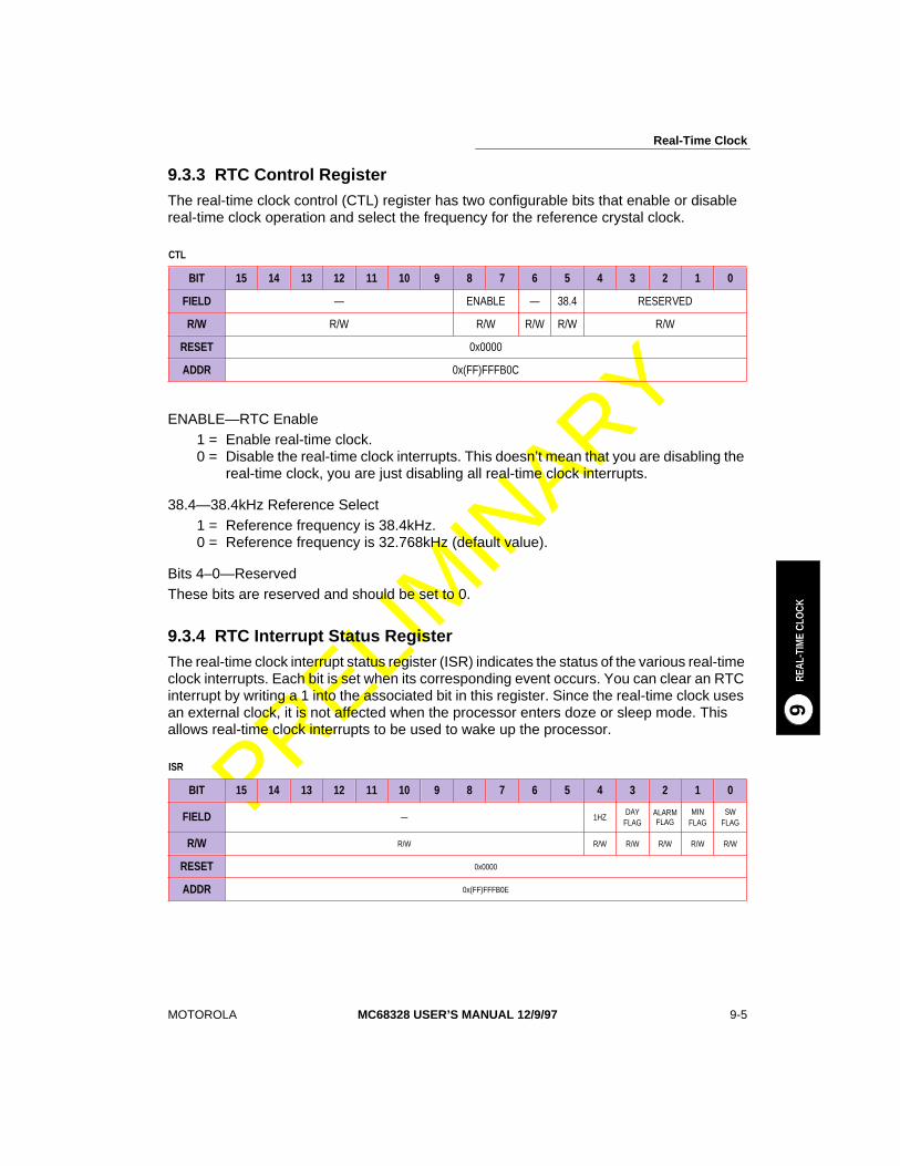
Real-Time Clock
MOTOROLA
MC68328 USER’S MANUAL 12/9/97
9-5
REAL
-TIM
E CL
OCK
9
PRELIM
INARY
9.3.3 RTC Control Register
The real-time clock control (CTL) register has two configurable bits that enable or disable real-time clock operation and select the frequency for the reference crystal clock.
ENABLE—RTC Enable1 = Enable real-time clock.0 = Disable the real-time clock interrupts. This doesn’t mean that you are disabling the
real-time clock, you are just disabling all real-time clock interrupts.
38.4—38.4kHz Reference Select1 = Reference frequency is 38.4kHz.0 = Reference frequency is 32.768kHz (default value).
Bits 4–0—ReservedThese bits are reserved and should be set to 0.
9.3.4 RTC Interrupt Status Register
The real-time clock interrupt status register (ISR) indicates the status of the various real-time clock interrupts. Each bit is set when its corresponding event occurs. You can clear an RTC interrupt by writing a 1 into the associated bit in this register. Since the real-time clock uses an external clock, it is not affected when the processor enters doze or sleep mode. This allows real-time clock interrupts to be used to wake up the processor.
CTL
BIT 15 14 13 12 11 10 9 8 7 6 5 4 3 2 1 0
FIELD
— ENABLE — 38.4 RESERVED
R/W
R/W R/W R/W R/W R/W
RESET
0x0000
ADDR
0x(FF)FFFB0C
ISR
BIT 15 14 13 12 11 10 9 8 7 6 5 4 3 2 1 0
FIELD
— 1HZDAY
FLAGALARMFLAG
MINFLAG
SWFLAG
R/W
R/W R/W R/W R/W R/W R/W
RESET
0x0000
ADDR
0x(FF)FFFB0E
Real-Time Clock
9-6
MC68328 USER’S MANUAL 12/9/97
MOTOROLA
REAL-TIME CLO
CK
9
PRELIM
INARY
1Hz FLAG—1Hz FlagWhen the 1Hz interrupt is enabled, this bit is set every second and an interrupt is generated to the processor.
1 = A 1Hz interrupt occurs.0 = No 1Hz interrupt occurs.
DAY FLAG—Day FlagWhen the 24-hour interrupt is enabled, this bit is set for every 24-hour clock increment (at midnight) and an interrupt is generated to the processor.
1 = A 24-hour rollover interrupt occurs.0 = No 24-hour rollover interrupt occurs.
ALARM FLAG—Alarm FlagWhen an alarm interrupt is enabled, this bit is set on a “compare” match between the real-time clock (current time) and the alarm register’s value. The alarm will reoccur every 24 hours. If a single alarm is required, you must clear the interrupt and disable the alarm interrupt in the RTC interrupt enable register.
1 = An alarm interrupt occurs.0 = No alarm interrupt occurs.
MIN FLAG—Minute FlagWhen a minute interrupt is enabled, this bit is set on every minute tick and an interrupt is generated to the processor.
1 = A minute tick occurs.0 = No minute tick occurs.
SW FLAG—Stopwatch FlagWhen a stopwatch interrupt is enabled, this bit is set when the stopwatch minute countdown counter goes from 00 to 3F and an interrupt is posted to the processor.
1 = The stopwatch timed out.0 = No stopwatch timed out.
Real-Time Clock
MOTOROLA
MC68328 USER’S MANUAL 12/9/97
9-7
REAL
-TIM
E CL
OCK
9
PRELIM
INARY
9.3.5 RTC Interrupt Enable Register
The real-time clock interrupt enable register (IENR) allows you to individually enable different real-time clock interrupts. The real-time clock provides five interrupts—a 1 second interrupt, 1 minute interrupt, 1 day (at midnight) interrupt, alarm interrupt, and a stopwatch interrupt. At reset, all RTC interrupts are disabled.
1HZEN—1Hz Interrupt EnableThis bit enables an interrupt at a 1Hz rate.
1 = A 1Hz interrupt is enabled.0 = A 1Hz interrupt is disabled.
24HREN—24-Hour Interrupt EnableThis bit enables an interrupt at midnight rollover.
1 = A 24-hour interrupt is enabled.0 = A 24-hour interrupt is disabled.
ALMEN—Alarm Interrupt EnableThis bit enables the alarm interrupt.
1 = An alarm interrupt is enabled.0 = An alarm interrupt is disabled.
MINEN—Minute Interrupt EnableThis bit enables the minute tick interrupt.
1 = A minute tick interrupt is enabled.0 = A minute tick interrupt is disabled.
IENR
BIT 15 14 13 12 11 10 9 8 7 6 5 4 3 2 1 0
FIELD
— 1HZEN 24HR EN ALM EN MINEN SWEN
R/W
R/W R/W R/W R/W R/W R/W
RESET
0x0000
ADDR
0x(FF)FFFB10
Real-Time Clock
9-8
MC68328 USER’S MANUAL 12/9/97
MOTOROLA
REAL-TIME CLO
CK
9
PRELIM
INARY
SWEN—Stopwatch Interrupt EnableThis bit enables the stopwatch interrupt.
1 = A stopwatch interrupt is enabled.0 = A stopwatch interrupt is disabled.
9.3.6 RTC STOPWATCH REGISTER
The real-time clock stopwatch (STPWCH) programmable register contains the countdown value. When the stopwatch interrupt is enabled, this countdown value is decremented every minute and an interrupt is posted when the countdown value reaches -1.
STOPWATCH COUNTThis field contains the stopwatch countdown value, which can be a maximum of 62 minutes. The countdown will not be activated again until a nonzero value (less than 63 minutes) is written to this register.
Note:
The stopwatch counts down and remains at 3F (hex) until it is reprogrammed. Ifthis bit is enabled with 3F (hex) in the RTC stopwatch register, an interrupt willbe posted on the next minute tick.
STPWCH
BIT 15 14 13 12 11 10 9 8 7 6 5 4 3 2 1 0
FIELD
— STOPWATCH COUNT
R/W
R/W R/W
RESET
0x0000
ADDR
0x(FF)FFFB12
MOTOROLA
MC68328 USER’S MANUAL 12/9/97
10-1
TIM
ERS
10
PRELIM
INARY
SECTION 10TIMERS
The DragonBall microprocessor contains two identical general-purpose 16-bit timers and a software watchdog timer. The block diagram of a timer module is illustrated in Figure 10-1.
10.1 FEATURES
The following list summarizes the main features of the general-purpose timers:
• Maximum Period of 524 Seconds at 32kHz
• 60ns Resolution at 16.67MHz
• Programmable Sources for the Clock Input, Including an External Clock
• Input Capture Capability with Programmable Trigger Edge on Input Pins
• Output Compare with Programmable Mode for the Output Pins
• Free Run and Restart Modes
The software watchdog timer has the following features:
• 16-Bit Counter and Reference Register
• Maximum Period of 16.38 Seconds
• 0.25ms Resolution
• Timeout Causes System Reset or a Maskable Interrupt
Figure 10-1. General-Purpose Timer Block Diagram
COMPARE REGISTER
COUNTER REGISTER
EVENT REGISTER
CAPTURE REGISTER
CONTROL REGISTER
CAPTURE DETECT
INTERRUPT
TIN
SYSTEM CLOCKPRESCALER
MPU BUSTOUT
TIMER CLOCK
PRESCALAR REGISTER32K HZ CLOCK
DIV 16
CLOCK GENERATOR
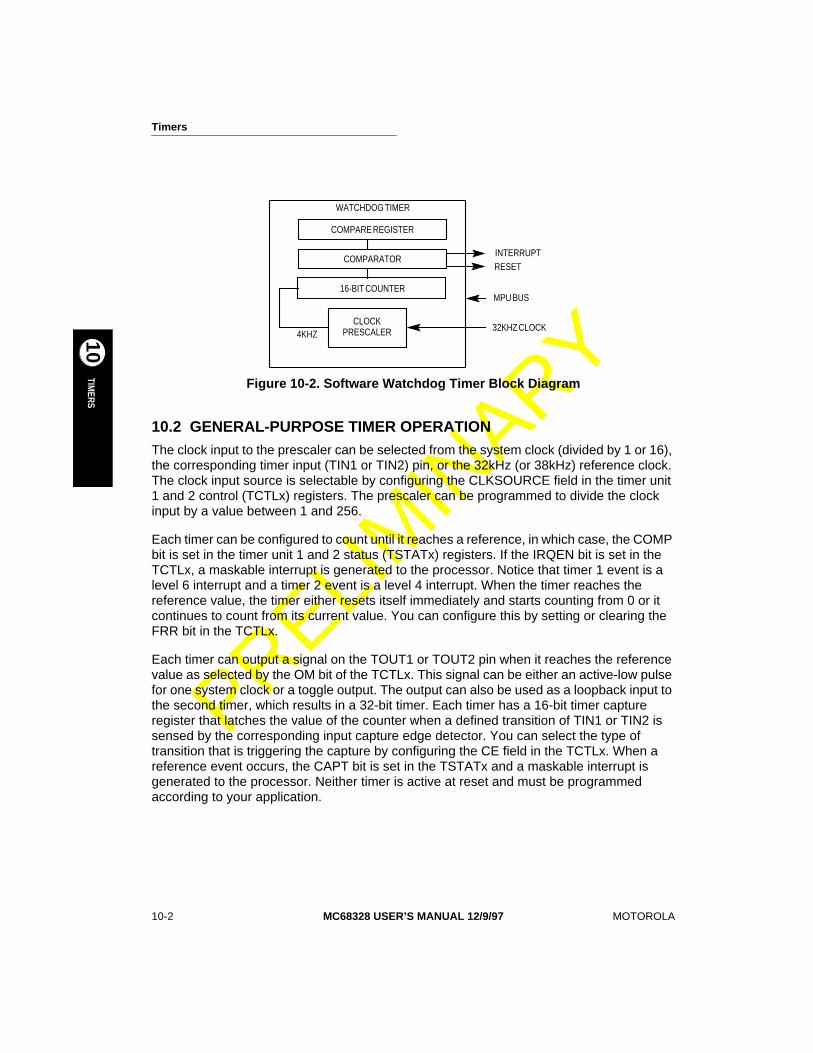
Timers
10-2
MC68328 USER’S MANUAL 12/9/97
MOTOROLA
TIMERS
10
PRELIM
INARY
10.2 GENERAL-PURPOSE TIMER OPERATION
The clock input to the prescaler can be selected from the system clock (divided by 1 or 16), the corresponding timer input (TIN1 or TIN2) pin, or the 32kHz (or 38kHz) reference clock. The clock input source is selectable by configuring the CLKSOURCE field in the timer unit 1 and 2 control (TCTLx) registers. The prescaler can be programmed to divide the clock input by a value between 1 and 256.
Each timer can be configured to count until it reaches a reference, in which case, the COMP bit is set in the timer unit 1 and 2 status (TSTATx) registers. If the IRQEN bit is set in the TCTLx, a maskable interrupt is generated to the processor. Notice that timer 1 event is a level 6 interrupt and a timer 2 event is a level 4 interrupt. When the timer reaches the reference value, the timer either resets itself immediately and starts counting from 0 or it continues to count from its current value. You can configure this by setting or clearing the FRR bit in the TCTLx.
Each timer can output a signal on the TOUT1 or TOUT2 pin when it reaches the reference value as selected by the OM bit of the TCTLx. This signal can be either an active-low pulse for one system clock or a toggle output. The output can also be used as a loopback input to the second timer, which results in a 32-bit timer. Each timer has a 16-bit timer capture register that latches the value of the counter when a defined transition of TIN1 or TIN2 is sensed by the corresponding input capture edge detector. You can select the type of transition that is triggering the capture by configuring the CE field in the TCTLx. When a reference event occurs, the CAPT bit is set in the TSTATx and a maskable interrupt is generated to the processor. Neither timer is active at reset and must be programmed according to your application.
Figure 10-2. Software Watchdog Timer Block Diagram
RESETCOMPARATOR
COMPARE REGISTER
CLOCK PRESCALER
16-BIT COUNTER
32KHZ CLOCK
MPU BUS
WATCHDOG TIMER
4KHZ
INTERRUPT
Timers
MOTOROLA
MC68328 USER’S MANUAL 12/9/97
10-3
TIM
ERS
10
PRELIM
INARY
10.3 SOFTWARE WATCHDOG TIMER OPERATION
The software watchdog timer protects against system failures by enabling you to escape from unexpected input conditions, external events, or programming errors. This dedicated 16-bit timer serves as the software watchdog timer.
You can program the watchdog compare register (WRR) with the timeout value. The watchdog counter will start counting from 0 until it reaches this timeout value. If your software does not clear the counter before it reaches the timeout, the timer assumes that a system failure has occurred and the software watchdog logic initiates either a soft reset of the chip or a maskable interrupt to the CPU, depending on the FI bit in the WRR. Therefore, once the software watchdog timer is enabled, your software must clear the software watchdog timer periodically so that it never reaches its timeout value. The maskable interrupt generated is cleared by clearing the watchdog counter.
The software watchdog timer uses the 32kHz clock as the input to its prescaler module. The prescaler circuitry divides the clock input by a fixed value of eight. The output of this prescaler circuitry is connected to the input of a 16-bit counter. The reference/compare register is a 16-bit programmable register that can be programmed with a maximum value of 65535 (or 0xFFFF in hex).
10.4 SIGNALS
The following signals are multiplexed with the Port G I/O signals. See
Section 7 Parallel Ports
for more information about enabling the timers.
• TIN1/PG6 and TIN2/PG4—This pin is the input to the timer and can be used in capture mode to latch the contents of the free-running counter. It can also serve as the source of the clock to the prescaler.
• TOUT1/PG5 and TOUT2/PG3—This pin is the output of the timer and can be programmed to toggle or pulse when a “compare” event occurs.
Note:
At reset, the watchdog timer is enabled by default when the WDEN bit is set inthe watchdog control and status register (WCSR). Depending on yourapplication, if you do not need the watchdog timer, you should turn it off in thesystem boot-up code. It is recommended that you turn the software watchdogtimer off before you put the processor in sleep or doze because the watchdogtimer will continue to run in these modes. The value of the software watchdogtimer counter can be read at any time.
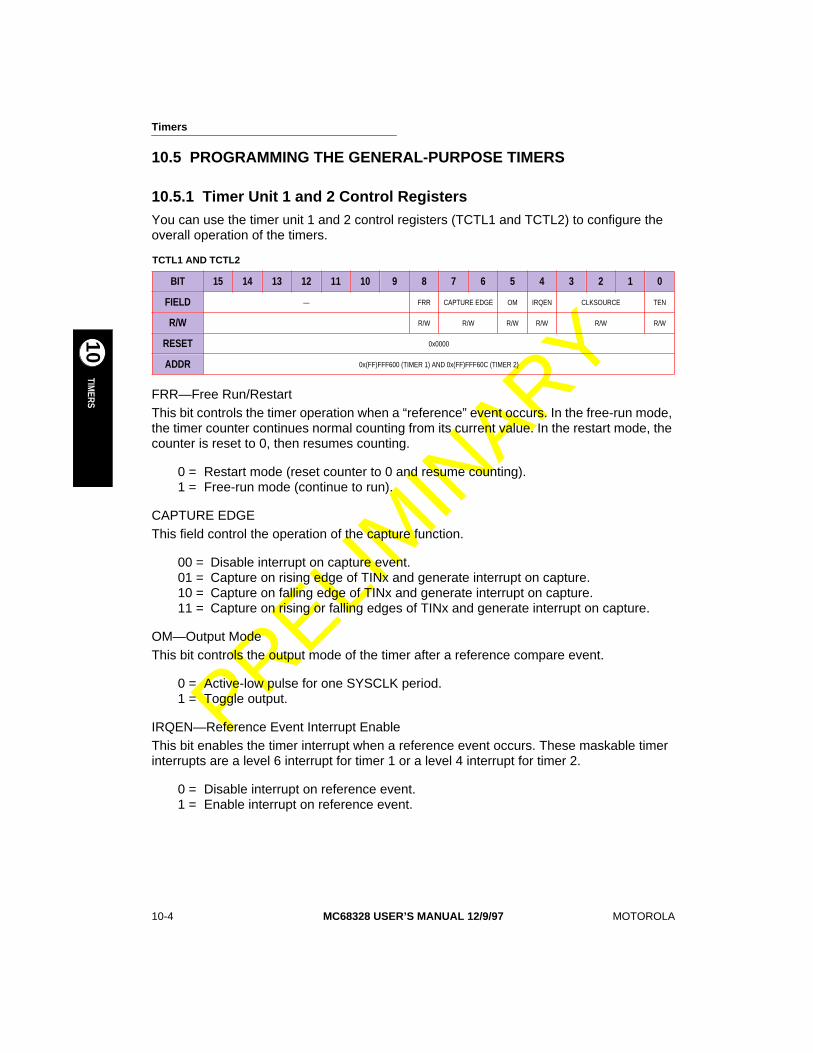
Timers
10-4
MC68328 USER’S MANUAL 12/9/97
MOTOROLA
TIMERS
10
PRELIM
INARY
10.5 PROGRAMMING THE GENERAL-PURPOSE TIMERS
10.5.1 Timer Unit 1 and 2 Control Registers
You can use the timer unit 1 and 2 control registers (TCTL1 and TCTL2) to configure the overall operation of the timers.
FRR—Free Run/RestartThis bit controls the timer operation when a “reference” event occurs. In the free-run mode, the timer counter continues normal counting from its current value. In the restart mode, the counter is reset to 0, then resumes counting.
0 = Restart mode (reset counter to 0 and resume counting).1 = Free-run mode (continue to run).
CAPTURE EDGEThis field control the operation of the capture function.
00 = Disable interrupt on capture event.01 = Capture on rising edge of TINx and generate interrupt on capture.10 = Capture on falling edge of TINx and generate interrupt on capture.11 = Capture on rising or falling edges of TINx and generate interrupt on capture.
OM—Output ModeThis bit controls the output mode of the timer after a reference compare event.
0 = Active-low pulse for one SYSCLK period.1 = Toggle output.
IRQEN—Reference Event Interrupt EnableThis bit enables the timer interrupt when a reference event occurs. These maskable timer interrupts are a level 6 interrupt for timer 1 or a level 4 interrupt for timer 2.
0 = Disable interrupt on reference event.1 = Enable interrupt on reference event.
TCTL1 AND TCTL2
BIT 15 14 13 12 11 10 9 8 7 6 5 4 3 2 1 0
FIELD
— FRR CAPTURE EDGE OM IRQEN CLKSOURCE TEN
R/W
R/W R/W R/W R/W R/W R/W
RESET
0x0000
ADDR
0x(FF)FFF600 (TIMER 1) AND 0x(FF)FFF60C (TIMER 2)
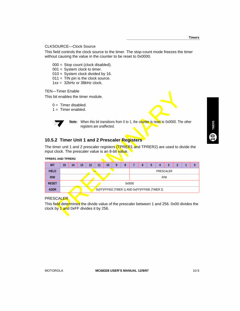
Timers
MOTOROLA
MC68328 USER’S MANUAL 12/9/97
10-5
TIM
ERS
10
PRELIM
INARY
CLKSOURCE—Clock SourceThis field controls the clock source to the timer. The stop-count mode freezes the timer without causing the value in the counter to be reset to 0x0000.
000 = Stop count (clock disabled).001 = System clock to timer.010 = System clock divided by 16.011 = TIN pin is the clock source.1xx = 32kHz or 38kHz clock.
TEN—Timer EnableThis bit enables the timer module.
0 = Timer disabled.1 = Timer enabled.
10.5.2 Timer Unit 1 and 2 Prescaler Registers
The timer unit 1 and 2 prescaler registers (TPRER1 and TPRER2) are used to divide the input clock. The prescaler value is an 8-bit value.
PRESCALERThis field determines the divide value of the prescaler between 1 and 256. 0x00 divides the clock by 1 and 0xFF divides it by 256.
Note:
When this bit transitions from 0 to 1, the counter is reset to 0x0000. The otherregisters are unaffected.
TPRER1 AND TPRER2
BIT 15 14 13 12 11 10 9 8 7 6 5 4 3 2 1 0
FIELD
— PRESCALER
R/W
R/W
RESET
0x0000
ADDR
0x(FF)FFF602 (TIMER 1) AND 0x(FF)FFF60E (TIMER 2)
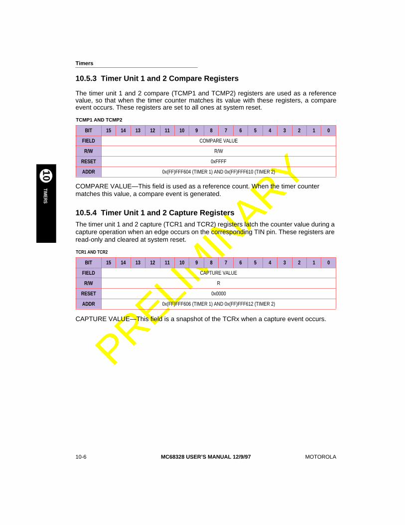
Timers
10-6
MC68328 USER’S MANUAL 12/9/97
MOTOROLA
TIMERS
10
PRELIM
INARY
10.5.3 Timer Unit 1 and 2 Compare Registers
The timer unit 1 and 2 compare (TCMP1 and TCMP2) registers are used as a referencevalue, so that when the timer counter matches its value with these registers, a compareevent occurs. These registers are set to all ones at system reset.
COMPARE VALUE—This field is used as a reference count. When the timer counter matches this value, a compare event is generated.
10.5.4 Timer Unit 1 and 2 Capture Registers
The timer unit 1 and 2 capture (TCR1 and TCR2) registers latch the counter value during a capture operation when an edge occurs on the corresponding TIN pin. These registers are read-only and cleared at system reset.
CAPTURE VALUE—This field is a snapshot of the TCRx when a capture event occurs.
TCMP1 AND TCMP2
BIT 15 14 13 12 11 10 9 8 7 6 5 4 3 2 1 0
FIELD
COMPARE VALUE
R/W
R/W
RESET
0xFFFF
ADDR
0x(FF)FFF604 (TIMER 1) AND 0x(FF)FFF610 (TIMER 2)
TCR1 AND TCR2
BIT 15 14 13 12 11 10 9 8 7 6 5 4 3 2 1 0
FIELD
CAPTURE VALUE
R/W
R
RESET
0x0000
ADDR
0x(FF)FFF606 (TIMER 1) AND 0x(FF)FFF612 (TIMER 2)
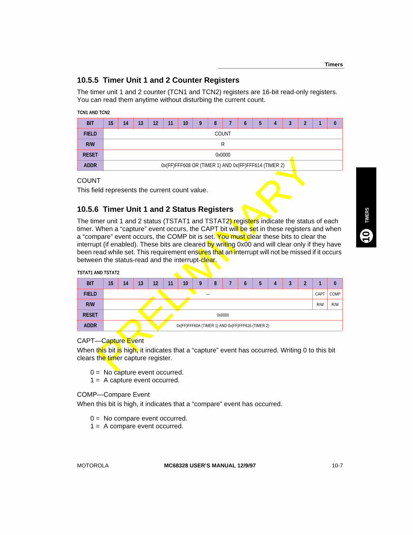
Timers
MOTOROLA
MC68328 USER’S MANUAL 12/9/97
10-7
TIM
ERS
10
PRELIM
INARY
10.5.5 Timer Unit 1 and 2 Counter Registers
The timer unit 1 and 2 counter (TCN1 and TCN2) registers are 16-bit read-only registers. You can read them anytime without disturbing the current count.
COUNTThis field represents the current count value.
10.5.6 Timer Unit 1 and 2 Status Registers
The timer unit 1 and 2 status (TSTAT1 and TSTAT2) registers indicate the status of each timer. When a “capture” event occurs, the CAPT bit will be set in these registers and when a “compare” event occurs, the COMP bit is set. You must clear these bits to clear the interrupt (if enabled). These bits are cleared by writing 0x00 and will clear only if they have been read while set. This requirement ensures that an interrupt will not be missed if it occurs between the status-read and the interrupt-clear.
CAPT—Capture EventWhen this bit is high, it indicates that a “capture” event has occurred. Writing 0 to this bit clears the timer capture register.
0 = No capture event occurred.1 = A capture event occurred.
COMP—Compare EventWhen this bit is high, it indicates that a “compare” event has occurred.
0 = No compare event occurred.1 = A compare event occurred.
TCN1 AND TCN2
BIT 15 14 13 12 11 10 9 8 7 6 5 4 3 2 1 0
FIELD
COUNT
R/W
R
RESET
0x0000
ADDR
0x(FF)FFF608 OR (TIMER 1) AND 0x(FF)FFF614 (TIMER 2)
TSTAT1 AND TSTAT2
BIT 15 14 13 12 11 10 9 8 7 6 5 4 3 2 1 0
FIELD
— CAPT COMP
R/W
R/W R/W
RESET
0x0000
ADDR
0x(FF)FFF60A (TIMER 1) AND 0x(FF)FFF616 (TIMER 2)
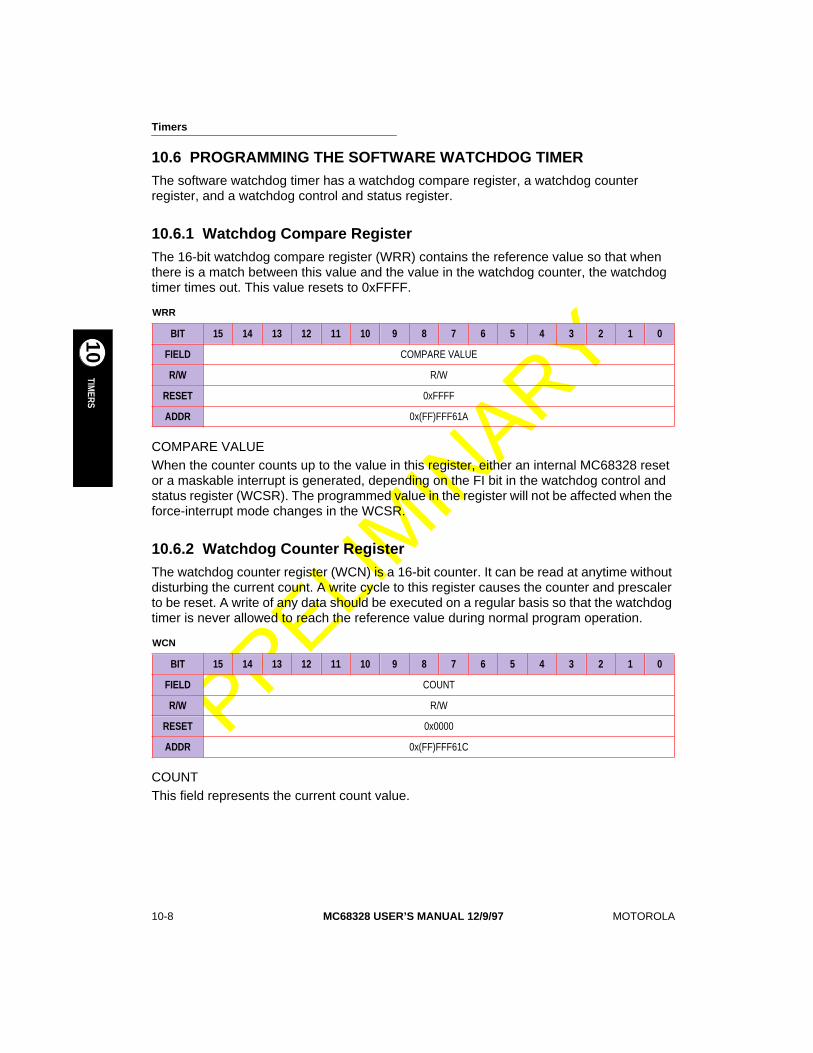
Timers
10-8
MC68328 USER’S MANUAL 12/9/97
MOTOROLA
TIMERS
10
PRELIM
INARY
10.6 PROGRAMMING THE SOFTWARE WATCHDOG TIMER
The software watchdog timer has a watchdog compare register, a watchdog counter register, and a watchdog control and status register.
10.6.1 Watchdog Compare Register
The 16-bit watchdog compare register (WRR) contains the reference value so that when there is a match between this value and the value in the watchdog counter, the watchdog timer times out. This value resets to 0xFFFF.
COMPARE VALUEWhen the counter counts up to the value in this register, either an internal MC68328 reset or a maskable interrupt is generated, depending on the FI bit in the watchdog control and status register (WCSR). The programmed value in the register will not be affected when the force-interrupt mode changes in the WCSR.
10.6.2 Watchdog Counter Register
The watchdog counter register (WCN) is a 16-bit counter. It can be read at anytime without disturbing the current count. A write cycle to this register causes the counter and prescaler to be reset. A write of any data should be executed on a regular basis so that the watchdog timer is never allowed to reach the reference value during normal program operation.
COUNTThis field represents the current count value.
WRR
BIT 15 14 13 12 11 10 9 8 7 6 5 4 3 2 1 0
FIELD
COMPARE VALUE
R/W
R/W
RESET
0xFFFF
ADDR
0x(FF)FFF61A
WCN
BIT 15 14 13 12 11 10 9 8 7 6 5 4 3 2 1 0
FIELD
COUNT
R/W
R/W
RESET
0x0000
ADDR
0x(FF)FFF61C
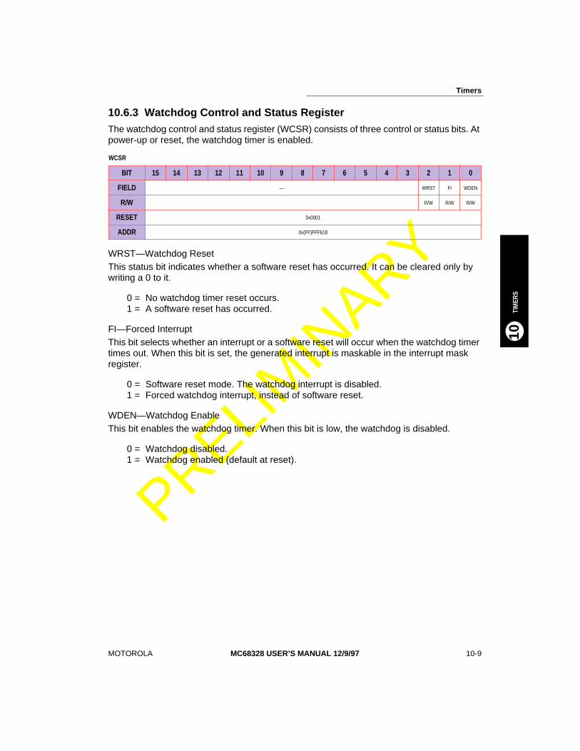
Timers
MOTOROLA
MC68328 USER’S MANUAL 12/9/97
10-9
TIM
ERS
10
PRELIM
INARY
10.6.3 Watchdog Control and Status Register
The watchdog control and status register (WCSR) consists of three control or status bits. At power-up or reset, the watchdog timer is enabled.
WRST—Watchdog ResetThis status bit indicates whether a software reset has occurred. It can be cleared only by writing a 0 to it.
0 = No watchdog timer reset occurs.1 = A software reset has occurred.
FI—Forced InterruptThis bit selects whether an interrupt or a software reset will occur when the watchdog timer times out. When this bit is set, the generated interrupt is maskable in the interrupt mask register.
0 = Software reset mode. The watchdog interrupt is disabled.1 = Forced watchdog interrupt, instead of software reset.
WDEN—Watchdog EnableThis bit enables the watchdog timer. When this bit is low, the watchdog is disabled.
0 = Watchdog disabled.1 = Watchdog enabled (default at reset).
WCSR
BIT 15 14 13 12 11 10 9 8 7 6 5 4 3 2 1 0
FIELD
— WRST FI WDEN
R/W
R/W R/W R/W
RESET
0x0001
ADDR
0x(FF)FFF618

Timers
10-10
MC68328 USER’S MANUAL 12/9/97
MOTOROLA
TIMERS
10
PRELIM
INARY
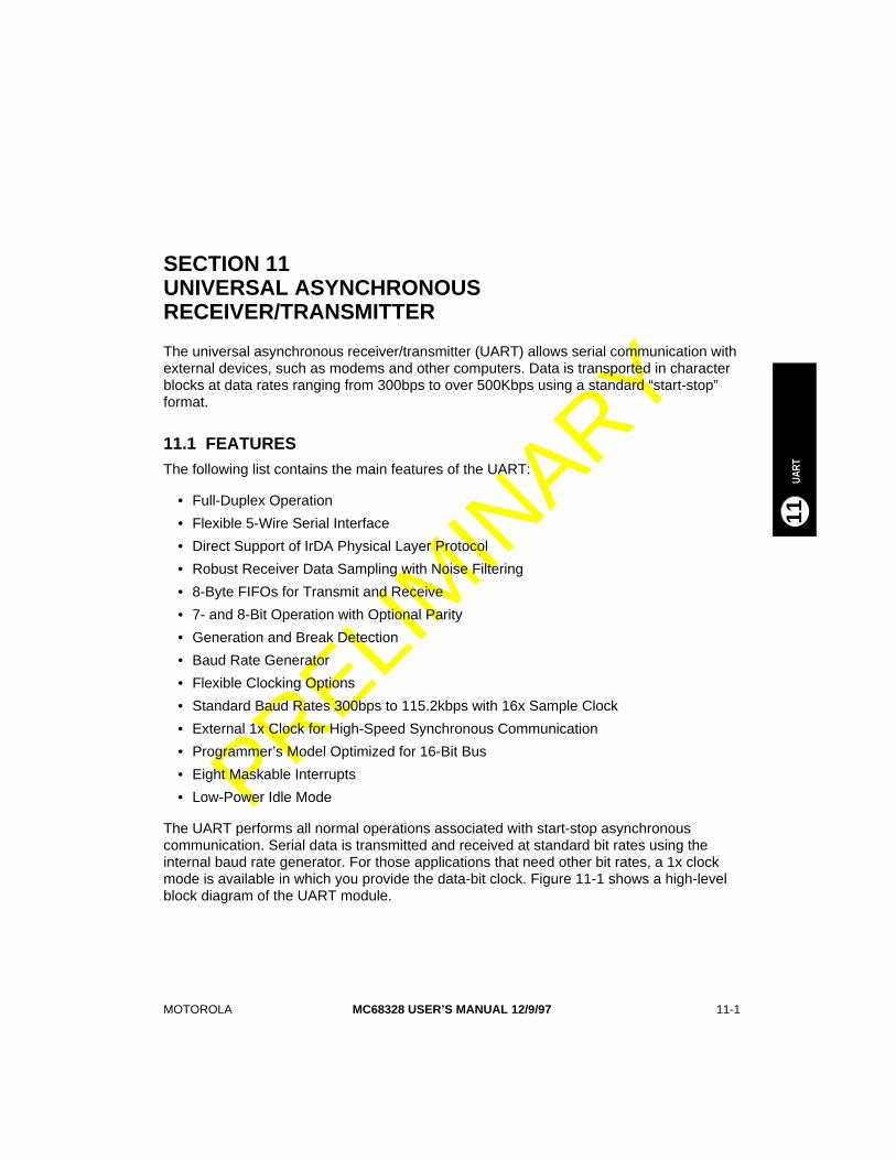
MOTOROLA
MC68328 USER’S MANUAL 12/9/97
11-1
UART
11
PRELIM
INARY
SECTION 11UNIVERSAL ASYNCHRONOUS RECEIVER/TRANSMITTER
The universal asynchronous receiver/transmitter (UART) allows serial communication with external devices, such as modems and other computers. Data is transported in character blocks at data rates ranging from 300bps to over 500Kbps using a standard “start-stop” format.
11.1 FEATURES
The following list contains the main features of the UART:
• Full-Duplex Operation
• Flexible 5-Wire Serial Interface
• Direct Support of IrDA Physical Layer Protocol
• Robust Receiver Data Sampling with Noise Filtering
• 8-Byte FIFOs for Transmit and Receive
• 7- and 8-Bit Operation with Optional Parity
• Generation and Break Detection
• Baud Rate Generator
• Flexible Clocking Options
• Standard Baud Rates 300bps to 115.2kbps with 16x Sample Clock
• External 1x Clock for High-Speed Synchronous Communication
• Programmer’s Model Optimized for 16-Bit Bus
• Eight Maskable Interrupts
• Low-Power Idle Mode
The UART performs all normal operations associated with start-stop asynchronous communication. Serial data is transmitted and received at standard bit rates using the internal baud rate generator. For those applications that need other bit rates, a 1x clock mode is available in which you provide the data-bit clock. Figure 11-1 shows a high-level block diagram of the UART module.
Universal Asynchronous Receiver/Transmitter
11-2
MC68328 USER’S MANUAL 12/9/97
MOTOROLA
UART
11
PRELIM
INARY
11.2 SERIAL INTERFACE SIGNALS
There are five UART signals that you can access. If you need any or all of the UART signals, the appropriate port bits can be programmed to assume their UART function. Refer to
Section 7 Parallel Ports
for information about programming the ports.
• TXD—The transmit data pin is the transmitter serial output. During normal mode, NRZ data is an output. In infra-red mode, a
3
/
16
bit period pulse is output for each 0 bit transmitted. For RS-232 applications, this pin must be connected to an RS-232 transmitter. For infra-red applications, this pin can directly drive an infra-red transceiver module.
• CTS—The clear-to-send pin is an active-low input that controls the transmitter. Normally, the transmitter waits until this signal is active (low) before transmitting a character. If the IGNORE CTS bit is set, the transmitter sends a character whenever a character is ready to transmit. This signal can then serve as a general-purpose input with a read status in the CTS STATUS bit. This pin can post an interrupt on any transition of itself if the interrupt is enabled.
• RXD—The receive data pin is the receiver serial input. During normal operation, NRZ (Non Return to Zero) data is expected. In infrared mode, a narrow pulse is expected for each 0 bit received. Use external circuitry to convert the infra-red signal to an electrical signal. RS-232 applications need an external RS-232 receiver to convert from RS-232 voltage levels.
Figure 11-1. UART Block Diagram
SER
IAL I
NTE
RFA
CE
MPU
INTE
RFA
CE
RECEIVER
TRANSMITTER
RX FIFO
TX FIFO GPIO
RTS
RXD
CTS
TXD
INFR
A-R
ED
INTE
RFA
CE
BAUD GENBA
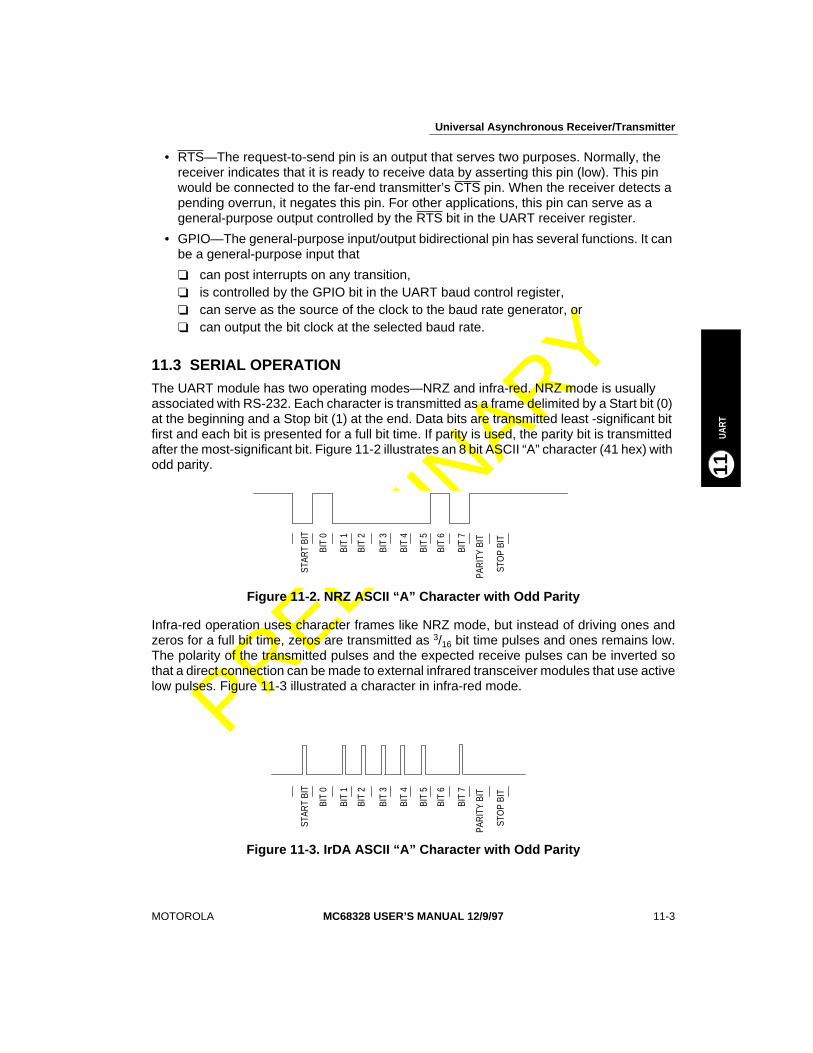
Universal Asynchronous Receiver/Transmitter
MOTOROLA
MC68328 USER’S MANUAL 12/9/97
11-3
UART
11
PRELIM
INARY
• RTS—The request-to-send pin is an output that serves two purposes. Normally, the receiver indicates that it is ready to receive data by asserting this pin (low). This pin would be connected to the far-end transmitter’s CTS pin. When the receiver detects a pending overrun, it negates this pin. For other applications, this pin can serve as a general-purpose output controlled by the RTS bit in the UART receiver register.
• GPIO—The general-purpose input/output bidirectional pin has several functions. It can be a general-purpose input that
❏
can post interrupts on any transition,
❏
is controlled by the GPIO bit in the UART baud control register,
❏
can serve as the source of the clock to the baud rate generator, or
❏
can output the bit clock at the selected baud rate.
11.3 SERIAL OPERATION
The UART module has two operating modes—NRZ and infra-red. NRZ mode is usually associated with RS-232. Each character is transmitted as a frame delimited by a Start bit (0) at the beginning and a Stop bit (1) at the end. Data bits are transmitted least -significant bit first and each bit is presented for a full bit time. If parity is used, the parity bit is transmitted after the most-significant bit. Figure 11-2 illustrates an 8 bit ASCII “A” character (41 hex) with odd parity.
Infra-red operation uses character frames like NRZ mode, but instead of driving ones andzeros for a full bit time, zeros are transmitted as
3
/
16
bit time pulses and ones remains low.The polarity of the transmitted pulses and the expected receive pulses can be inverted sothat a direct connection can be made to external infrared transceiver modules that use activelow pulses. Figure 11-3 illustrated a character in infra-red mode.
Figure 11-2. NRZ ASCII “A” Character with Odd Parity
Figure 11-3. IrDA ASCII “A” Character with Odd Parity
STAR
T BI
T
BIT
0
BIT
1
BIT
2
BIT
3
BIT
4
BIT
5
BIT
6
BIT
7
PAR
ITY
BIT
STO
P BI
T
STAR
T BI
T
BIT
0
BIT
1
BIT
2
BIT
3
BIT
4
BIT
5
BIT
6
BIT
7
PAR
ITY
BIT
STO
P BI
T
Universal Asynchronous Receiver/Transmitter
11-4
MC68328 USER’S MANUAL 12/9/97
MOTOROLA
UART
11
PRELIM
INARY
The UART module is easy to use from both a hardware and a software perspective. Five working registers provide all of the status and control functions and they are optimized for a 16-bit bus. For example, all status bits associated with the received data are available along with the data byte in a single 16-bit read. All register bits are readable and most are read/write.
The modem control signals are flexible. CTS is an input that can provide hardware flow-control to the transmitter or it can serve as a general-purpose input. A maskable interrupt is posted on each transition of this signal. RTS is an output from the receiver that indicates that the receiver has space in the FIFO for data. This bit can be configured as a general-purpose output. A GPIO pin is provided that can bring an external bit-clock into the module. It can also serve as a general-purpose input with a maskable interrupt posted on each transition. It can be configured as an output that provides a bit clock or a signal under software control. The UART module consists of a transmitter, a reciever, a baud rate generator, and an MPU interface.
11.3.1 Transmitter
The transmitter accepts a character (a byte) from the MPU bus and transmits it serially. While the FIFO is empty, the transmitter outputs continuous idle (1 in NRZ mode and 0 in infra-red mode). When a character is available for transmission, the START, STOP, and PARITY (if enabled) bits are added to the character and it is serially shifted at the selected bit rate. The transmitter posts a maskable interrupt when it needs
more data from the CPU. Three interrupts are available. If you want to take full advantage of the 8-byte FIFO, the FIFO empty interrupt should be enabled. In the interrupt service routine, the FIFO should be interrogated after each byte is loaded. If space is available (the TX AVAIL bit is set), more data will be loaded into the FIFO. The transmitter will not generate another interrupt until the FIFO has completely emptied. If you have a system that has a large interrupt service latency, use the FIFO half interrupt. In this case, the transmitter generates an interrupt when the FIFO occupancy is less than 4 bytes. If the FIFO is not needed, use the TX avail interrupt. An interrupt will be generated whenever at least one space is available in the FIFO.
CTS can control the serial data flow. If CTS is negated (high), the transmitter finishes sending the character in progress (if any), then waits for CTS to again become asserted (low) for the next transmission. Set the SEND BREAK bit in the UART transmitter register to generate a break character (continuous 0s). Your software must know the baud rate. The SEND BREAK bit must be asserted for a sufficient amount of time to generate a valid break character. You can generate parity errors for debugging purposes. The transmitter operates from the 1x clock provided by the baud rate generator.
While the infra-red interface is enabled, the transmitter produces a pulse that is
3
/
16
of a bit time for each 0 bit that is sent. The TXD port directly interfaces with popular infra-red transceivers.
Universal Asynchronous Receiver/Transmitter
MOTOROLA
MC68328 USER’S MANUAL 12/9/97
11-5
UART
11
PRELIM
INARY
11.3.2 Receiver
The receiver accepts a serial datastream and converts it into a parallel character. It operates in two modes—16x and 1x. In 16x mode, it searches for a START bit, qualifies it, then samples the succeeding data bits at the bit center. Jitter tolerance and noise immunity are provided by sampling at a 16x rate and using a voting technique to clean up the samples. In 1x mode, RXD is sampled on each rising edge of the bit clock.
After locating the START bit, the DATA bits, PARITY bit (if enabled), and STOP bits are shifted in. If PARITY is enabled, parity checking is performed and its status is reported in the UART receiver register. Similarly, frame errors and breaks are checked and reported. When the host is ready to read a new character, RTS is asserted and an interrupt is posted (if enabled). When the receiver register is read as a 16-bit word, the core reads the complete FIFO status, the four STATUS bits, and the received character byte. The RTS pin can be configured as an output to indicate when the receiver is ready for data or software can directly control the pin.
As with the transmitter, the receiver FIFO is flexible. If your software has a short interrupt latency, the FIFO full interrupt can be enabled. Only one space is available in the FIFO when this interrupt is generated. By reading the receiver register as a word, the FIFO status is presented to the processor along with the data. If the FIFO status indicates that data remains in the FIFO, the FIFO can then be emptied byte-by-byte. If the software has a longer latency, the FIFO half interrupt is used. This interrupt is generated when 4 bytes have been entered into the FIFO. If the FIFO is not needed, the data ready interrupt is used. This interrupt is generated whenever one or more characters are present in the FIFO.
When the infra-red mode is enabled, the receiver expects narrow pulses for each 0 bit received; otherwise, normal NRZ is expected. An infra-red transceiver, external to the DragonBall microprocessor, transforms the infra-red signal into an electrical signal.
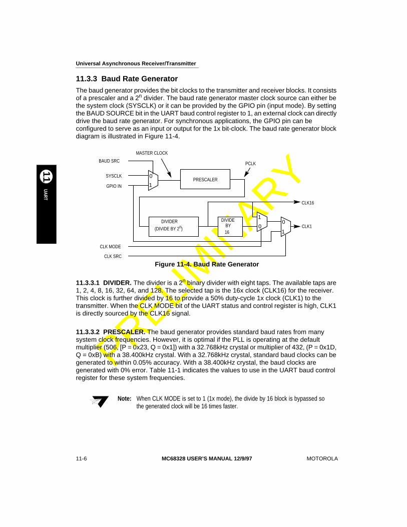
Universal Asynchronous Receiver/Transmitter
11-6
MC68328 USER’S MANUAL 12/9/97
MOTOROLA
UART
11
PRELIM
INARY
11.3.3 Baud Rate Generator
The baud generator provides the bit clocks to the transmitter and receiver blocks. It consists of a prescaler and a 2
n
divider. The baud rate generator master clock source can either be the system clock (SYSCLK) or it can be provided by the GPIO pin (input mode). By setting the BAUD SOURCE bit in the UART baud control register to 1, an external clock can directly drive the baud rate generator. For synchronous applications, the GPIO pin can be configured to serve as an input or output for the 1x bit-clock. The baud rate generator block diagram is illustrated in Figure 11-4.
11.3.3.1 DIVIDER.
The divider is a 2
n
binary divider with eight taps. The available taps are 1, 2, 4, 8, 16, 32, 64, and 128. The selected tap is the 16x clock (CLK16) for the receiver. This clock is further divided by 16 to provide a 50% duty-cycle 1x clock (CLK1) to the transmitter. When the CLK MODE bit of the UART status and control register is high, CLK1 is directly sourced by the CLK16 signal.
11.3.3.2 PRESCALER.
The baud generator provides standard baud rates from many system clock frequencies. However, it is optimal if the PLL is operating at the default multiplier (506, [P = 0x23, Q = 0x1]) with a 32.768kHz crystal or multiplier of 432, (P = 0x1D, Q = 0xB) with a 38.400kHz crystal. With a 32.768kHz crystal, standard baud clocks can be generated to within 0.05% accuracy. With a 38.400kHz crystal, the baud clocks are generated with 0% error. Table 11-1 indicates the values to use in the UART baud control register for these system frequencies.
Figure 11-4. Baud Rate Generator
Note:
When CLK MODE is set to 1 (1x mode), the divide by 16 block is bypassed sothe generated clock will be 16 times faster.
DIVIDER DIVIDE
(DIVIDE BY 2n)BY16
PRESCALER0
1
0
1
BAUD SRC
SYSCLK
GPIO IN
CLK16
CLK1
CLK SRC
0
1
MASTER CLOCK
PCLK
CLK MODE
Universal Asynchronous Receiver/Transmitter
MOTOROLA
MC68328 USER’S MANUAL 12/9/97
11-7
UART
11
PRELIM
INARY
11.3.4 MPU Interface
The MPU interface includes all status and control registers and all miscellaneous logic. This block directly connects to the internal 68000 bus and provides address decode for three address lines and a full 16-bit read/write port. The interrupt line is the logical-OR of the eight interrupt sources. When the UART EN bit is low, the master clock to all UART blocks is disabled, thus keeping power consumption to a minimum.
11.4 PROGRAMMING MODEL
11.4.1 UART Status and Control Register
The UART status and control (USTCNT) register controls overall UART operation.
UART EN—UART EnableThis bit enables the UART. When this bit is low, the UART is disabled to save power. When it is high, the UART is active. This bit resets to 0.
0 = UART disabled.1 = UART enabled.
RX EN—Receiver EnableThis bit enables the receiver block. When this bit is low, the receiver is disabled and the receive FIFO is flushed. This bit resets to 0.
0 = Receiver disabled and receive FIFO flushed.1 = Receiver enabled.
USTCNT
BIT 15 14 13 12 11 10 9 8 7 6 5 4 3 2 1 0
FIELD
UART EN RX EN TX EN CLK
MODEPARITY
ENODD EVEN STOP 8/7
GPIO DELTA
EN
CTS DELTA
EN
RX FULLEN
RX HALF
EN
RX RDY EN
TX EMPTY
EN
TX HALF
EN
TX AVAIL
EN
R/W
R/W R/W R/W R/W R/W R/W R/W R/W R/W R/W R/W R/W R/W R/W R/W R/W
RESET
0x0000
ADDR
0x(FF)FFF900
Note:
When the UART is first enabled after a cold reset (before enabling interrupts) setthe UARTEN and RXEN bits and perform a word-read operation on the UARTreceiver register to initialize the FIFO and character status bits.
Universal Asynchronous Receiver/Transmitter
11-8
MC68328 USER’S MANUAL 12/9/97
MOTOROLA
UART
11
PRELIM
INARY
TX EN—Transmitter EnableThis bit enables the transmitter block. When this bit is low, the transmitter is disabled and the transmit FIFO is flushed. This bit resets to 0.
0 = Transmitter disabled and transmit FIFO flushed.1 = Transmitter enabled.
CLK MODE—Receiver Clock ModeThis bit controls the operating mode of the receiver. When this bit is low, the receiver is in 16x mode where it synchronizes to the incoming data stream and samples at the perceived center of each bit period. When this bit is high, the receiver is in 1x mode where it samples the datastream on each rising edge of the bit clock. This bit resets to 0.
0 = 16x clock mode.1 = 1x clock mode.
PAR EN—Parity EnableThis bit controls the parity generator in the transmitter and parity checker in the receiver. When this bit is high, they are enabled and when it is low, they are disabled.
0 = Parity disabled.1 = Parity enabled.
ODD EVEN—Odd or Even Parity SelectionThis bit controls the sense of the parity generator and checker. When this bit is high, odd parity is generated on the transmitter and expected on the receiver. When it is low, even parity is generated and expected. This bit has no function if PARITY EN is low.
0 = Even parity.1 = Odd parity.
STOP—STOP Bit SelectionThis bit controls the number of stop bits transmitted after a character. When this bit is high, two stop bits are sent and when it is low, one stop bit is sent. This bit has no effect on the receiver, which expects one or more stop bits.
0 = One STOP bit transmitted.1 = Two STOP bits transmitted.
8/7—Character Word LengthThis bit controls the character length. When this bit is high, the transmitter and receiver are in 8-bit mode. When it is low, they are in 7-bit mode. The transmitter then ignores B7 and the receiver sets B7 to 0.
0 = 7 transmit and receive bits per character.1 = 8 transmit and receive bits per character.
Universal Asynchronous Receiver/Transmitter
MOTOROLA
MC68328 USER’S MANUAL 12/9/97
11-9
UART
11
PRELIM
INARY
GPIO DELTA EN—General-Purpose I/O Delta EnableThis bit enables an interrupt when the GPIO pin (while configured as an input) changes state. The current state of the GPIO pin is read in the UART baud control register.
0 = GPIO interrupt disabled.1 = GPIO interrupt enabled.
CTS DELTA EN—CTS Delta EnableWhen this bit is high, it enables an interrupt when the CTS pin changes state. When this bit is low, this interrupt is disabled. The current status of the CTS pin is read in the UART transmitter register.
0 = CTS interrupt disabled.1 = CTS interrupt enabled.
RX FULL EN—Receiver Full EnableWhen this bit is high, it enables an interrupt when the receiver FIFO is full. This bit resets to 0.
0 = RX full interrupt disabled.1 = RX full interrupt enabled.
RX HALF EN—Receiver Half EnableWhen this bit is high, it enables an interrupt when the receiver FIFO is more than half full. This bit resets to 0.
0 = RX half interrupt disabled.1 = RX half interrupt enabled.
RX RDY EN—Receiver Ready EnableWhen this bit is high, it enables an interrupt when the receiver has at least one data byte in the FIFO. When it is low, this interrupt is disabled. This bit resets to 0.
0 = RX interrupt disabled.1 = RX interrupt enabled.
TX EMPTY EN—Transmitter Empty EnableWhen this bit is high, it enables an interrupt when the transmitter FIFO is empty and needs data. When it is low, this interrupt is disabled. This bit resets to 0.
0 = TX empty interrupt disabled.1 = TX empty interrupt enabled.
Universal Asynchronous Receiver/Transmitter
11-10
MC68328 USER’S MANUAL 12/9/97
MOTOROLA
UART
11
PRELIM
INARY
TX HALF EN—Transmitter Half EnableWhen this bit is high, it enables an interrupt when the transmit FIFO is less than half full. When it is low, the TX half interrupt is disabled. This bit resets to 0.
0 = TX half interrupt disabled.1 = TX half interrupt enabled.
TX AVAIL EN—Transmitter Available EnableWhen this bit is high, it enables an interrupt when the transmitter has a slot available in the FIFO. When it is low, this interrupt is disabled. This bit resets to 0.
0 = TX avail interrupt disabled.1 = TX avail interrupt enabled.
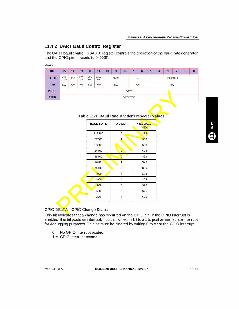
Universal Asynchronous Receiver/Transmitter
MOTOROLA
MC68328 USER’S MANUAL 12/9/97
11-11
UART
11
PRELIM
INARY
11.4.2 UART Baud Control Register
The UART baud control (UBAUD) register controls the operation of the baud-rate generator and the GPIO pin. It resets to 0x003F.
GPIO DELTA—GPIO Change StatusThis bit indicates that a change has occurred on the GPIO pin. If the GPIO interrupt is enabled, this bit posts an interrupt. You can write this bit to a 1 to post an immediate interrupt for debugging purposes. This bit must be cleared by writing 0 to clear the GPIO interrupt.
0 = No GPIO interrupt posted.1 = GPIO interrupt posted.
UBAUD
BIT 15 14 13 12 11 10 9 8 7 6 5 4 3 2 1 0
FIELD
GPIO DELTA GPIO GPIO
DIRGPIO SRC
BAUD SRC DIVIDE — PRESCALER
R/W
R/W R/W R/W R/W R/W R/W R/W R/W
RESET
0x003F
ADDR
0x(FF)FFF902
Table 11-1. Baud Rate Divider/Prescaler Values
BAUD RATE DIVIDER PRESCALER (HEX)
115200 0 $38
57600 1 $38
28800 2 $38
14400 3 $38
38400 0 $26
19200 1 $26
9600 2 $26
4800 3 $26
2400 4 $26
1200 5 $26
600 6 $26
300 7 $26
Universal Asynchronous Receiver/Transmitter
11-12 MC68328 USER’S MANUAL 12/9/97 MOTOROLA
UART11
PRELIM
INARY
GPIO—GPIO Status/ControlIf GPIO is configured as an input, this bit indicates the current state of the GPIO pin. If GPIO is configured as an output, this bit controls the state of the pin.
0 = GPIO pin is low.1 = GPIO pin is high.
GPIO DIR—GPIO DirectionThis bit controls the direction of the GPIO pin. When this bit is high, the pin is an input. When this bit is low, GPIO is an output.
0 = GPIO is input.1 = GPIO is output.
GPIO SRC—GPIO SourceThis bit controls the source of the GPIO pin. When high, the source is the 1x clock from the baud rate generator. When low, the source is the GPIO bit. When the GPIO DIR bit is 0, this bit has no function.
0 = GPIO driven by GPIO bit.1 = GPIO driven by a bit clock from the baud rate generator.
BAUD SRC—Baud SourceThis bit controls the clock source to the baud rate generator.
0 = Baud rate generator source is a system clock.1 = Baud rate generator source is the GPIO pin (GPIO DIR must be 0).
DIVIDER—Clock DividerThis field controls the clock frequency produced by the baud rate generator. The bits are encoded as follows:
000 = Divide by 1.001 = Divide by 2.010 = Divide by 4.011 = Divide by 8.100 = Divide by 16.101 = Divide by 32.110 = Divide by 64.111 = Divide by 128.
PRESCALER—Clock PrescalerThis field controls the divide value of the baud rate generator prescaler. The divide value is determined by the following formula:
prescaler divide value = 65 (decimal) - PRESCALER
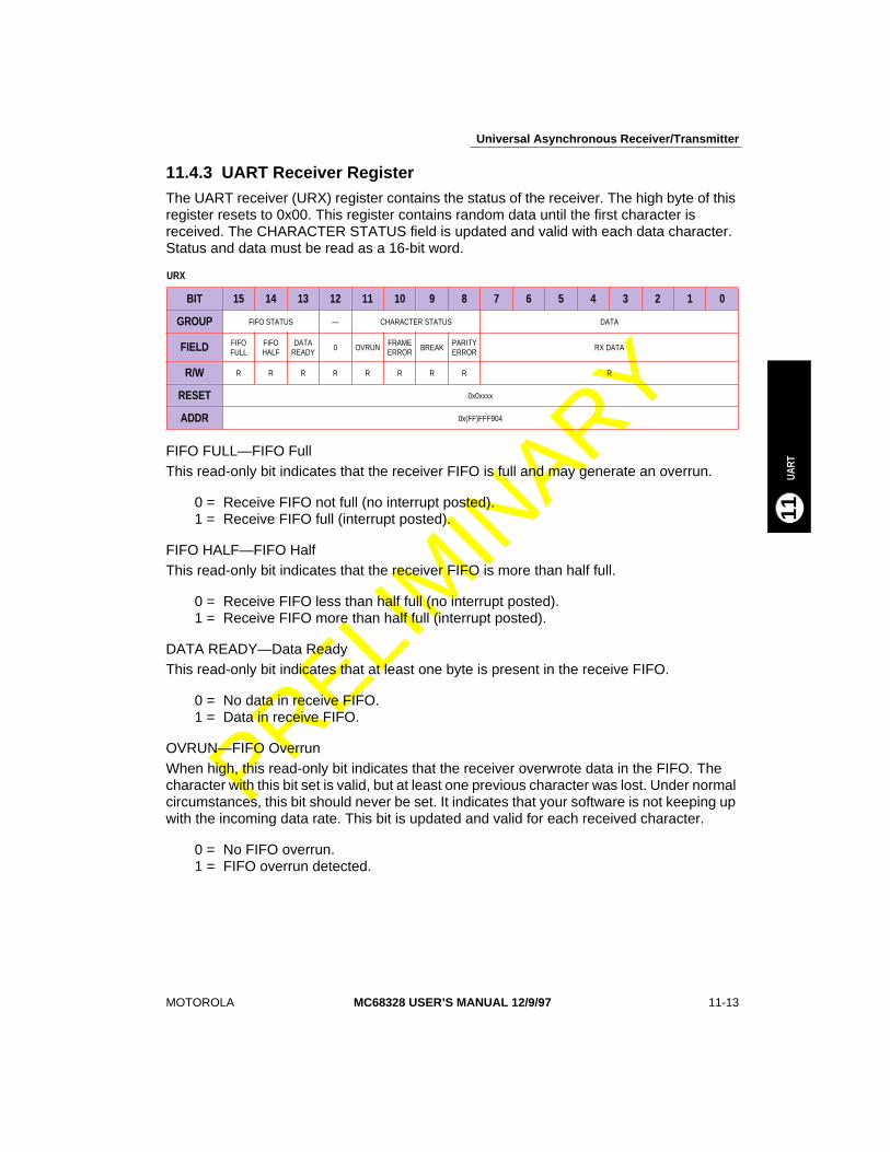
Universal Asynchronous Receiver/Transmitter
MOTOROLA MC68328 USER’S MANUAL 12/9/97 11-13
UART
11PRELI
MIN
ARY
11.4.3 UART Receiver RegisterThe UART receiver (URX) register contains the status of the receiver. The high byte of this register resets to 0x00. This register contains random data until the first character is received. The CHARACTER STATUS field is updated and valid with each data character. Status and data must be read as a 16-bit word.
FIFO FULL—FIFO FullThis read-only bit indicates that the receiver FIFO is full and may generate an overrun.
0 = Receive FIFO not full (no interrupt posted).1 = Receive FIFO full (interrupt posted).
FIFO HALF—FIFO HalfThis read-only bit indicates that the receiver FIFO is more than half full.
0 = Receive FIFO less than half full (no interrupt posted).1 = Receive FIFO more than half full (interrupt posted).
DATA READY—Data ReadyThis read-only bit indicates that at least one byte is present in the receive FIFO.
0 = No data in receive FIFO.1 = Data in receive FIFO.
OVRUN—FIFO OverrunWhen high, this read-only bit indicates that the receiver overwrote data in the FIFO. The character with this bit set is valid, but at least one previous character was lost. Under normal circumstances, this bit should never be set. It indicates that your software is not keeping up with the incoming data rate. This bit is updated and valid for each received character.
0 = No FIFO overrun.1 = FIFO overrun detected.
URX
BIT 15 14 13 12 11 10 9 8 7 6 5 4 3 2 1 0
GROUP FIFO STATUS — CHARACTER STATUS DATA
FIELD FIFO FULL
FIFO HALF
DATA READY 0 OVRUN FRAME
ERROR BREAK PARITY ERROR RX DATA
R/W R R R R R R R R R
RESET 0x0xxxx
ADDR 0x(FF)FFF904
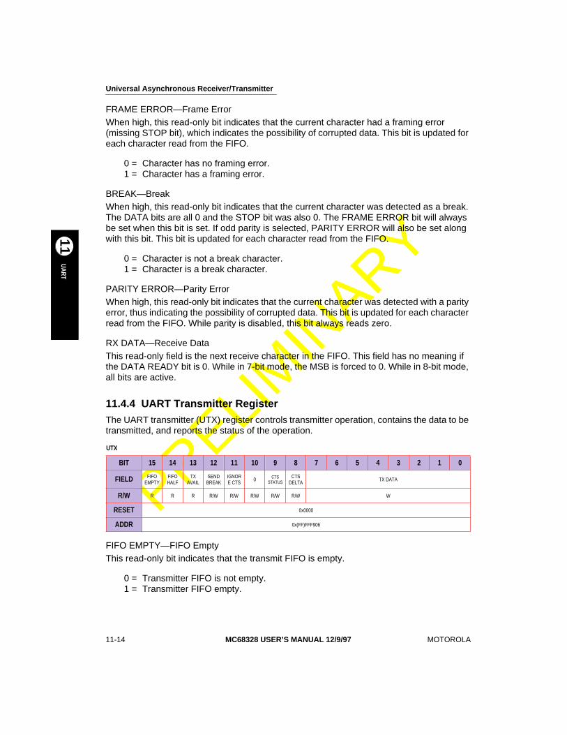
Universal Asynchronous Receiver/Transmitter
11-14 MC68328 USER’S MANUAL 12/9/97 MOTOROLA
UART11
PRELIM
INARY
FRAME ERROR—Frame ErrorWhen high, this read-only bit indicates that the current character had a framing error (missing STOP bit), which indicates the possibility of corrupted data. This bit is updated for each character read from the FIFO.
0 = Character has no framing error.1 = Character has a framing error.
BREAK—BreakWhen high, this read-only bit indicates that the current character was detected as a break. The DATA bits are all 0 and the STOP bit was also 0. The FRAME ERROR bit will always be set when this bit is set. If odd parity is selected, PARITY ERROR will also be set along with this bit. This bit is updated for each character read from the FIFO.
0 = Character is not a break character.1 = Character is a break character.
PARITY ERROR—Parity ErrorWhen high, this read-only bit indicates that the current character was detected with a parity error, thus indicating the possibility of corrupted data. This bit is updated for each character read from the FIFO. While parity is disabled, this bit always reads zero.
RX DATA—Receive Data This read-only field is the next receive character in the FIFO. This field has no meaning if the DATA READY bit is 0. While in 7-bit mode, the MSB is forced to 0. While in 8-bit mode, all bits are active.
11.4.4 UART Transmitter RegisterThe UART transmitter (UTX) register controls transmitter operation, contains the data to be transmitted, and reports the status of the operation.
FIFO EMPTY—FIFO EmptyThis read-only bit indicates that the transmit FIFO is empty.
0 = Transmitter FIFO is not empty.1 = Transmitter FIFO empty.
UTX
BIT 15 14 13 12 11 10 9 8 7 6 5 4 3 2 1 0
FIELD FIFO EMPTY
FIFO HALF
TX AVAIL
SEND BREAK
IGNORE CTS 0 CTS
STATUSCTS
DELTA TX DATA
R/W R R R R/W R/W R/W R/W R/W W
RESET 0x0000
ADDR 0x(FF)FFF906
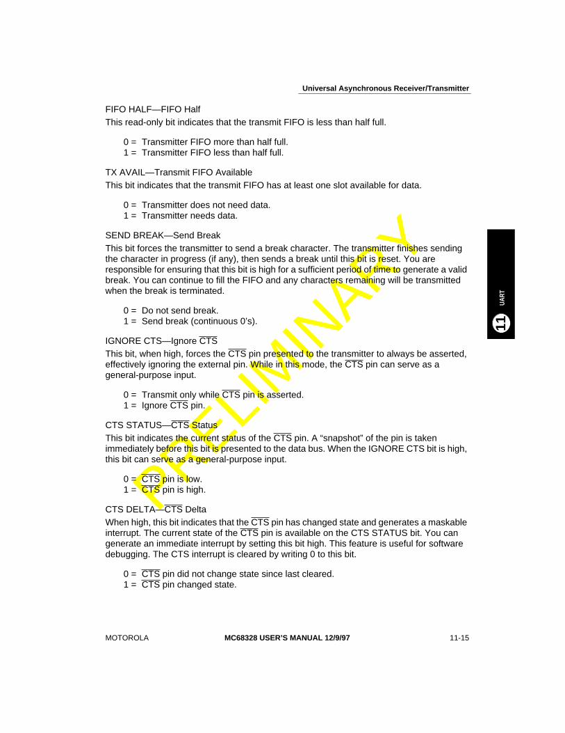
Universal Asynchronous Receiver/Transmitter
MOTOROLA MC68328 USER’S MANUAL 12/9/97 11-15
UART
11PRELI
MIN
ARY
FIFO HALF—FIFO HalfThis read-only bit indicates that the transmit FIFO is less than half full.
0 = Transmitter FIFO more than half full.1 = Transmitter FIFO less than half full.
TX AVAIL—Transmit FIFO AvailableThis bit indicates that the transmit FIFO has at least one slot available for data.
0 = Transmitter does not need data.1 = Transmitter needs data.
SEND BREAK—Send BreakThis bit forces the transmitter to send a break character. The transmitter finishes sending the character in progress (if any), then sends a break until this bit is reset. You are responsible for ensuring that this bit is high for a sufficient period of time to generate a valid break. You can continue to fill the FIFO and any characters remaining will be transmitted when the break is terminated.
0 = Do not send break.1 = Send break (continuous 0’s).
IGNORE CTS—Ignore CTSThis bit, when high, forces the CTS pin presented to the transmitter to always be asserted, effectively ignoring the external pin. While in this mode, the CTS pin can serve as a general-purpose input.
0 = Transmit only while CTS pin is asserted.1 = Ignore CTS pin.
CTS STATUS—CTS StatusThis bit indicates the current status of the CTS pin. A “snapshot” of the pin is taken immediately before this bit is presented to the data bus. When the IGNORE CTS bit is high, this bit can serve as a general-purpose input.
0 = CTS pin is low.1 = CTS pin is high.
CTS DELTA—CTS DeltaWhen high, this bit indicates that the CTS pin has changed state and generates a maskable interrupt. The current state of the CTS pin is available on the CTS STATUS bit. You can generate an immediate interrupt by setting this bit high. This feature is useful for software debugging. The CTS interrupt is cleared by writing 0 to this bit.
0 = CTS pin did not change state since last cleared.1 = CTS pin changed state.
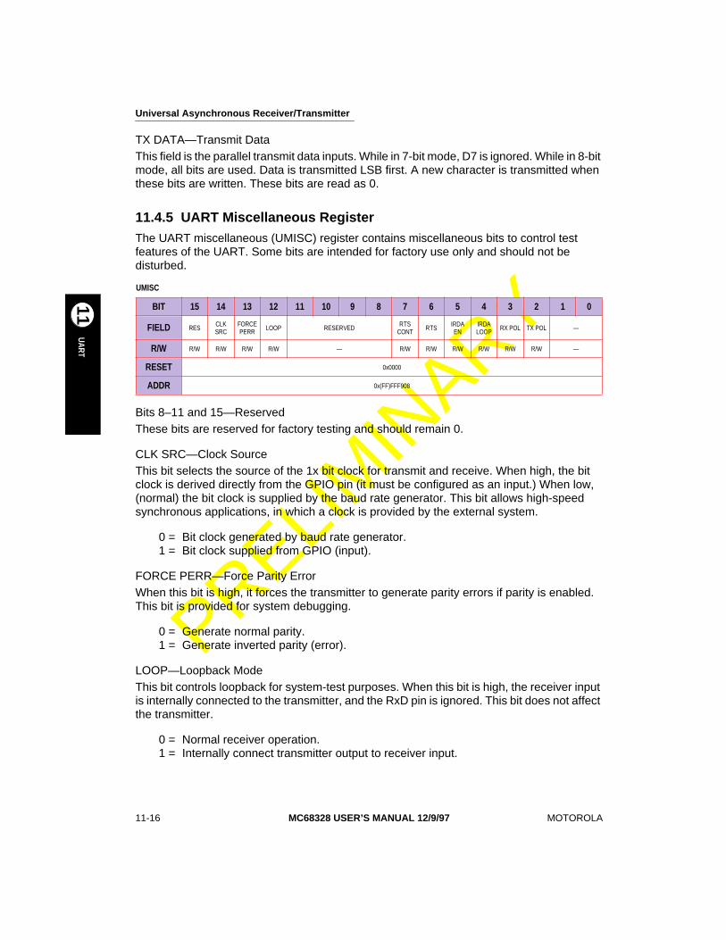
Universal Asynchronous Receiver/Transmitter
11-16 MC68328 USER’S MANUAL 12/9/97 MOTOROLA
UART11
PRELIM
INARY
TX DATA—Transmit DataThis field is the parallel transmit data inputs. While in 7-bit mode, D7 is ignored. While in 8-bit mode, all bits are used. Data is transmitted LSB first. A new character is transmitted when these bits are written. These bits are read as 0.
11.4.5 UART Miscellaneous RegisterThe UART miscellaneous (UMISC) register contains miscellaneous bits to control test features of the UART. Some bits are intended for factory use only and should not be disturbed.
Bits 8–11 and 15—ReservedThese bits are reserved for factory testing and should remain 0.
CLK SRC—Clock SourceThis bit selects the source of the 1x bit clock for transmit and receive. When high, the bit clock is derived directly from the GPIO pin (it must be configured as an input.) When low, (normal) the bit clock is supplied by the baud rate generator. This bit allows high-speed synchronous applications, in which a clock is provided by the external system.
0 = Bit clock generated by baud rate generator.1 = Bit clock supplied from GPIO (input).
FORCE PERR—Force Parity ErrorWhen this bit is high, it forces the transmitter to generate parity errors if parity is enabled. This bit is provided for system debugging.
0 = Generate normal parity.1 = Generate inverted parity (error).
LOOP—Loopback ModeThis bit controls loopback for system-test purposes. When this bit is high, the receiver input is internally connected to the transmitter, and the RxD pin is ignored. This bit does not affect the transmitter.
0 = Normal receiver operation.1 = Internally connect transmitter output to receiver input.
UMISC
BIT 15 14 13 12 11 10 9 8 7 6 5 4 3 2 1 0
FIELD RES CLK SRC
FORCE PERR LOOP RESERVED RTS
CONT RTS IRDA EN
IRDA LOOP RX POL TX POL —
R/W R/W R/W R/W R/W — R/W R/W R/W R/W R/W R/W —
RESET 0x0000
ADDR 0x(FF)FFF908
Universal Asynchronous Receiver/Transmitter
MOTOROLA MC68328 USER’S MANUAL 12/9/97 11-17
UART
11PRELI
MIN
ARY
RTS CONT—RTS ControlThis bit selects the function of the RTS pin.
0 = RTS pin is controlled by the RTS bit.1 = RTS pin is controlled by the receiver FIFO. When the FIFO is full (one slot
remaining) RTS is negated.
RTS—Request To SendThis bit controls the RTS pin while the RTS CONT bit is 0.
0 = RTS pin is 1.1 = RTS pin is 0.
IRDA EN—IrDA EnableThis bit enables the infra-red interface.
0 = Normal NRZ operation.1 = Infra-red operation.
LOOP IR—Loopback Mode for Infra-RedThis bit controls a loopback from transmitter to receiver in the infrared interface. This bit is provided for system testing.
0 = No infra-red loop.1 = Connect infra-red transmit to infra-red receiver.
RX POL—Receiver PolarityThis bit controls the expected polarity of the received data.
0 = Normal polarity 1 = Idle (0 = infra-red idle).1 = Inverted polarity 0 = idle (1 = infra-red idle).
TX POL—Transmitter PolarityThis bit controls the polarity of the transmitted data.
0 = Normal polarity 1 = Idle (0 = infra-red idle).1 = Inverted polarity 0 = Idle (1 = infra-red idle).

Universal Asynchronous Receiver/Transmitter
11-18 MC68328 USER’S MANUAL 12/9/97 MOTOROLA
UART11
PRELIM
INARY
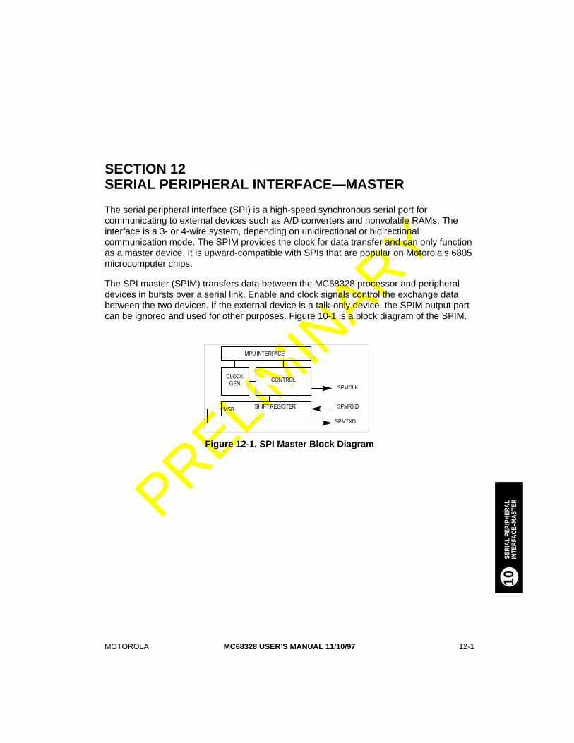
MOTOROLA
MC68328 USER’S MANUAL 11/10/97
12-1
SERI
AL P
ERIP
HERA
L
10
INTE
RFAC
E–M
ASTE
R
PRELIM
INARY
SECTION 12SERIAL PERIPHERAL INTERFACE—MASTER
The serial peripheral interface (SPI) is a high-speed synchronous serial port for communicating to external devices such as A/D converters and nonvolatile RAMs. The interface is a 3- or 4-wire system, depending on unidirectional or bidirectional communication mode. The SPIM provides the clock for data transfer and can only function as a master device. It is upward-compatible with SPIs that are popular on Motorola’s 6805 microcomputer chips.
The SPI master (SPIM) transfers data between the MC68328 processor and peripheral devices in bursts over a serial link. Enable and clock signals control the exchange data between the two devices. If the external device is a talk-only device, the SPIM output port can be ignored and used for other purposes. Figure 10-1 is a block diagram of the SPIM.
Figure 12-1. SPI Master Block Diagram
SPMCLK
CLOCKGEN
CONTROL
SHIFT REGISTER
MPU INTERFACE
SPMRXD
SPMTXD
MSB
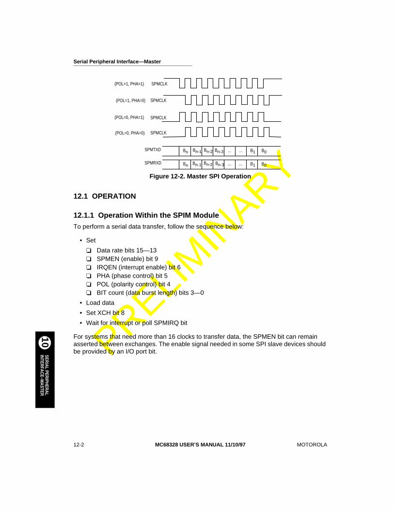
Serial Peripheral Interface—Master
12-2
MC68328 USER’S MANUAL 11/10/97
MOTOROLA
SERIAL PERIPHERAL
10
INTERFACE–MASTER
PRELIM
INARY
12.1 OPERATION
12.1.1 Operation Within the SPIM Module
To perform a serial data transfer, follow the sequence below:
• Set
❏
Data rate bits 15—13
❏
SPMEN (enable) bit 9
❏
IRQEN (interrupt enable) bit 6
❏
PHA (phase control) bit 5
❏
POL (polarity control) bit 4
❏
BIT count (data burst length) bits 3—0
• Load data
• Set XCH bit 8
• Wait for interrupt or poll SPMIRQ bit
For systems that need more than 16 clocks to transfer data, the SPMEN bit can remain asserted between exchanges. The enable signal needed in some SPI slave devices should be provided by an I/O port bit.
Figure 12-2. Master SPI Operation
SPMCLK
SPMRXD Bn ... ... B1 B0
SPMCLK
SPMCLK
SPMCLK(POL=1, PHA=1)
(POL=1, PHA=0)
(POL=0, PHA=1)
(POL=0, PHA=0)
SPMTXD Bn ... ... B1 B0Bn-1 Bn-2
Bn-1
Bn-3
Bn-3Bn-2
Serial Peripheral Interface—Master
MOTOROLA
MC68328 USER’S MANUAL 11/10/97
12-3
SERI
AL P
ERIP
HERA
L
10
INTE
RFAC
E–M
ASTE
R
PRELIM
INARY
12.1.2 Phase/Polarity Configurations
The SPIM transfers data in and out of the shift register with the SPICLK. Data is clocked using any one of the variations of clock phase and clock polarity. The clocked transfer may be programmed in phase and in polarity (Figure 12-2). In
phase 0
operation, output data changes on falling clock edges, while input data is shifted on rising edges. In a
phase 1
operation, output data changes on rising edges of the clock and is shifted on falling edges.
Polarity = 1
inverts the data-clock relationships. This flexibility allows operation with most serial peripheral devices on the market.
12.2 SIGNAL DESCRIPTIONS
The following signals are multiplexed with other signals in port K. Refer to
Section 7.1.10
for more information.
SPMTxD—TRANSMIT DATA
This pin is the shift-register output. A new data bit is presented on each rising edge of the SPMCLK in normal mode or on each falling edge of SPMCLK in inverted mode.
SPMRxD—RECEIVE DATA
This pin is the shift-register input. A new bit is shifted in on each falling edge of SPMCLK while in normal mode or on each rising edge of SPMCLK in inverted mode.
SPMCLK—SHIFT CLOCK
This pin is the clock output. When the SPIM is enabled, a selectable number of clock pulses is issued. While POL = 0, this signal is low while the SPIM is idle. When POL = 1, this signal is high during idle.
12.3 SPI MASTER REGISTERS
These registers control the SPIM operation and report its status. The data register exchanges data with external slave devices. After reset, all bits are set to $0000.
12.3.1 SPI Master Control/Status Register
This register controls the SPIM operation and reports its status.
15 14 13 12 11 10 9 8 7 6 5 4 3 2 1 0
DATA RATE RES RES RESSPIMEN
XCHSPIMIRQ
IRQEN
PHA POL BIT COUNT
ADDRESS: (FF)FFF802 RESET VALUE: $0000
Serial Peripheral Interface—Master
12-4
MC68328 USER’S MANUAL 11/10/97
MOTOROLA
SERIAL PERIPHERAL
10
INTERFACE–MASTER
PRELIM
INARY
DATA RATEThese bits select the baud rate of the SPMCLK based of divisions of the system clock. The master clock for the SPIM is SYSCLK. The bits are encoded as:
000 = Divide by 4001 = Divide by 8010 = Divide by 16011 = Divide by 32100 = Divide by 64101 = Divide by 128110 = Divide by 256111 = Divide by 512
SPIMEN—SPI Master EnableThis bit enables the SPIM. The enable should be asserted before initiating an exchange and should be negated after the exchange is complete. This bit must be set before data can be written into the SPIM data register.
0 = SPI master disable1 = SPI master enable
XCHThis bit triggers the state machine to generate (n= clock count) clocks at the selected bit rate. After the n-bit transfer, new data may be loaded and another exchange initiated. At least 2 SPI clocks should elapse before re-enabling this bit. This bit remains set until the transfer is completed.
1 = Initiate exchange0 = SPI is idle or exchange in progress
SPIMIRQ—SPI Master Interrupt RequestAn interrupt is asserted at the end of an exchange (assuming IRQEN is enabled). This bit is asserted until users clear it by writing a 0. Users can write these bits to generate an IRQ on demand. This bit can also be polled with IRQEN bit clear.
0 = No interrupt posted1 = Interrupt posted
Note:
To ensure a complete exchange, users should check the SPIMIRQ bit ratherthan XCH bit. The IRQEN should be on. Users not wanting to receive interruptupon completion of exchange can disable the incoming SPIM interrupt bymasking it in the IMR in the interrupt controller.
Serial Peripheral Interface—Master
MOTOROLA
MC68328 USER’S MANUAL 11/10/97
12-5
SERI
AL P
ERIP
HERA
L
10
INTE
RFAC
E–M
ASTE
R
PRELIM
INARY
IRQEN—Interrupt Request EnableThis bit will enable the SPIM interrupt. This bit is cleared to 0 on reset and must be enabled by software.
0 = Interrupts disabled1 = Interrupts enabled
PHA—PhaseThis bit controls the SPMCLK phase shift.
0 = Normal phase1 = Shift advance to opposite phase
POL—PolarityThis bit controls the SPMCLK polarity.
0 = Active-high polarity (0=idle)1 = Inverted polarity (1= idle)
BIT COUNTThese bits select the transfer length (up to 16 bits can be transferred).
0000 = 1 bit transfer 1111 = 16 bit transfer
12.3.2 SPIM Data Register
This register exchanges data with external slave devices.
DATAThese are the data bits to be exchanged with the external device. The data must be loaded before the XCH bit is set. At the end of the exchange, data from the peripheral is present in this register. These bits contain unknown data if they are read while the XCH bit is set. A write to these bits will be ignored while the XCH bit is set. As data is shifted MSB first, outgoing data is automatically MSB-justified. For example, if the exchange length is 10 bits, the MSB of the outgoing data is bit 9. The first bit presented to the external slave device will be bit 9, followed by the remaining 9 bits.
15 14 13 12 11 10 9 8 7 6 5 4 3 2 1 0
DATA
ADDRESS: (FF)FFF800 RESET VALUE: $0000
Note:
Users should reload the data every time for each transfer before setting the XCHbit.
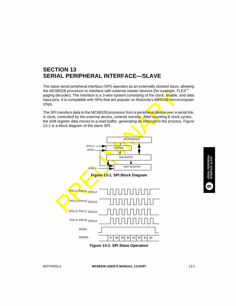
MOTOROLA
MC68328 USER’S MANUAL 11/10/97
13-1
SERI
AL P
ERIP
HERA
L
9
INTE
RFAC
E–SL
AVE
PRELIM
INARY
SECTION 13SERIAL PERIPHERAL INTERFACE—SLAVE
The slave serial peripheral interface (SPI) operates as an externally clocked slave, allowing the MC68328 processor to interface with external master devices (for example, FLEX
™
paging decoder). The interface is a 3-wire system consisting of the clock, enable, and data input pins. It is compatible with SPIs that are popular on Motorola’s 68HC05 microcomputer chips.
The SPI transfers data to the MC68328 processor from a peripheral device over a serial link. A clock, controlled by the external device, controls transfer. After counting 8 clock cycles, the shift register data moves to a read buffer, generating an interrupt in the process. Figure 13-1 is a block diagram of the slave SPI.
Figure 13-1. SPI Block Diagram
Figure 13-2. SPI Slave Operation
SHIFT REGISTER
MPU INTERFACE
SPSRXD
SPSCLK
SPSENCONTROL
DATA BUFFER
SPSCLK
SPSRXD B7 B6 B5 B4 B3 B2 B1 B0
SPSCLK
SPSCLK
SPSCLK(POL=1, PHA=1)
(POL=1, PHA=0)
(POL=0, PHA=1)
(POL=0, PHA=0)
SPSEN
Serial Peripheral Interface—Slave
13-2
MC68328 USER’S MANUAL 11/10/97
MOTOROLA
SERIAL PERIPHERAL
9
INTERFACE–SLAVE
PRELIM
INARY
13.1 OPERATION
Users first initialize the SPI slave (SPIS) program register. The SPIS then waits for the input-enable (SPSEN) and clock (SPSCLK) to control the data transfer. The shift register fills with data over the next 8 clock cycles. On the eighth clock, the shift register contents loads into the data buffer. The SPISIRQ bit is set, posting an interrupt. The valid data in the buffer awaits the service routine access.
The clock input performs shifts depending on phase and polarity. In
phase 0
mode(PHA=0), serial data are strobed on the leading edges of SPSCLK. In
phase 1
mode(PHA=1), data are strobed in on trailing edges. The
polarity (POL)
specifies the inactive state value of SPSCLK. While POL=1, the idle state of the SPSCLK is high. While POL = 0, the idle state of the SPSCLK is low. This flexibility allows operation with most serial peripheral devices on the market.
If enabled, the SPIS operates even if the system clock is inactive. After the SPIS receives a data byte from an external master, the SPIS interrupt is posted. If the system is in sleep mode, this interrupt can initiate the wakeup sequence for restoring the system clock. The SPIS bit (bit 21) in the wakeup control register IWR (at location 0x(FF)FFF308) must be set for the wakeup sequence to occur.
13.2 SIGNAL DESCRIPTIONS
SPSRXD
This pin is the serial data input to the shift register. A new bit is shifted in on each leading edge of SPSCLK while in normal mode(POL=0) or on each trailing edge of SPSCLK in polarity-inverted mode(POL=1). This signal pin is multiplexed with other signals to port K, bit 4. Refer to Section 7.1.10
for more details.
SPSCLK
This pin is the shift clock input.
SPSEN
This pin indicates that an SPI transfer is in progress. After the enable becomes active, the SPIS state machine responds to clock edges for data transfer.
13.3 SPI SLAVE REGISTER
This register controls the SPIS operation and reports its status. The data register contains the data transmitted by the external master. After reset, all bits are set to $0000.
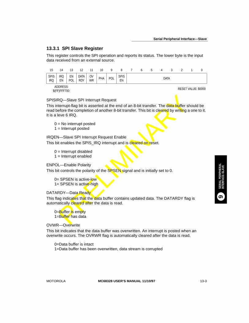
Serial Peripheral Interface—Slave
MOTOROLA
MC68328 USER’S MANUAL 11/10/97
13-3
SERI
AL P
ERIP
HERA
L
9
INTE
RFAC
E–SL
AVE
PRELIM
INARY
13.3.1 SPI Slave Register
This register controls the SPI operation and reports its status. The lower byte is the input data received from an external source.
SPISIRQ—Slave SPI Interrupt RequestThis interrupt-flag bit is asserted at the end of an 8-bit transfer. The data buffer should be read before the completion of another 8-bit transfer. This bit is cleared by writing a one to it. It is a leve 6 IRQ.
0 = No interrupt posted1 = Interrupt posted
IRQEN—Slave SPI Interrupt Request EnableThis bit enables the SPIS_IRQ interrupt and is cleared on reset.
0 = Interrupt disabled1 = Interrupt enabled
ENPOL—Enable PolarityThis bit controls the polarity of the SPSEN signal and is initially set to 0.
0= SPSEN is active-low 1= SPSEN is active-high
DATARDY—Data ReadyThis flag indicates that the data buffer contains updated data. The DATARDY flag is automatically cleared after the data is read.
0=Buffer is empty1=Buffer has data
OVWR—OverwriteThis bit indicates that the data buffer was overwritten. An interrupt is posted when an overwrite occurs. The OVRWR flag is automatically cleared after the data is read.
0=Data buffer is intact1=Data buffer has been overwritten, data stream is corrupted
15 14 13 12 11 10 9 8 7 6 5 4 3 2 1 0
SPIS IRQ
IRQEN
ENPOL
DATA RDY
OVWR
PHA POL SPISEN
DATA
ADDRESS: $(FF)FFF700:
RESET VALUE: $0000
Serial Peripheral Interface—Slave
13-4
MC68328 USER’S MANUAL 11/10/97
MOTOROLA
SERIAL PERIPHERAL
9
INTERFACE–SLAVE
PRELIM
INARY
PHA—PhaseThis bit sets the phase relationship between SPSCLK and SPSRxD. Refer to Figure 9-2.
0 = Phase 0 (normal); data is captured on the leading edge of SPSCLK1 = Phase 1; data is captured on the trailing edge of SPSCLK
POL—PolarityThis bit controls the polarity of the SPSCLK.
0 = The inactive state value of the clock is low (idle = 0)1 = The inactive state value of the clock is high (idle = 1)
SPISEN—Slave SPI EnableThis status bit enables the slave SPI module.
1 = SPIS module enabled0 = SPIS module disabled (default)
DATAThese are the data bits shifted from the external device. At every 8th SPSCLK edge, data from the peripheral is loaded into this buffered register. If the data buffer is not accessed before the next byte is received, it will be overwritten and the OVRWR bit will be set, posting an interrupt.
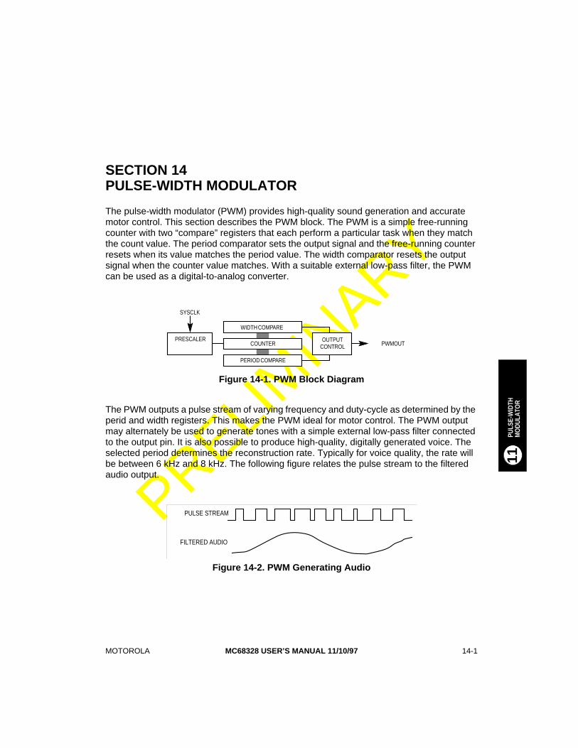
MOTOROLA
MC68328 USER’S MANUAL 11/10/97
14-1
PULS
E-W
IDTH
11
MO
DULA
TOR
PRELIM
INARY
SECTION 14PULSE-WIDTH MODULATOR
The pulse-width modulator (PWM) provides high-quality sound generation and accurate motor control. This section describes the PWM block. The PWM is a simple free-running counter with two “compare” registers that each perform a particular task when they match the count value. The period comparator sets the output signal and the free-running counter resets when its value matches the period value. The width comparator resets the output signal when the counter value matches. With a suitable external low-pass filter, the PWM can be used as a digital-to-analog converter.
The PWM outputs a pulse stream of varying frequency and duty-cycle as determined by the perid and width registers. This makes the PWM ideal for motor control. The PWM output may alternately be used to generate tones with a simple external low-pass filter connected to the output pin. It is also possible to produce high-quality, digitally generated voice. The selected period determines the reconstruction rate. Typically for voice quality, the rate will be between 6 kHz and 8 kHz. The following figure relates the pulse stream to the filtered audio output.
Figure 14-1. PWM Block Diagram
Figure 14-2. PWM Generating Audio
WIDTH COMPARE
PWMOUTOUTPUT
CONTROLPRESCALER
PERIOD COMPARE
COUNTER
SYSCLK
PULSE STREAM
FILTERED AUDIO
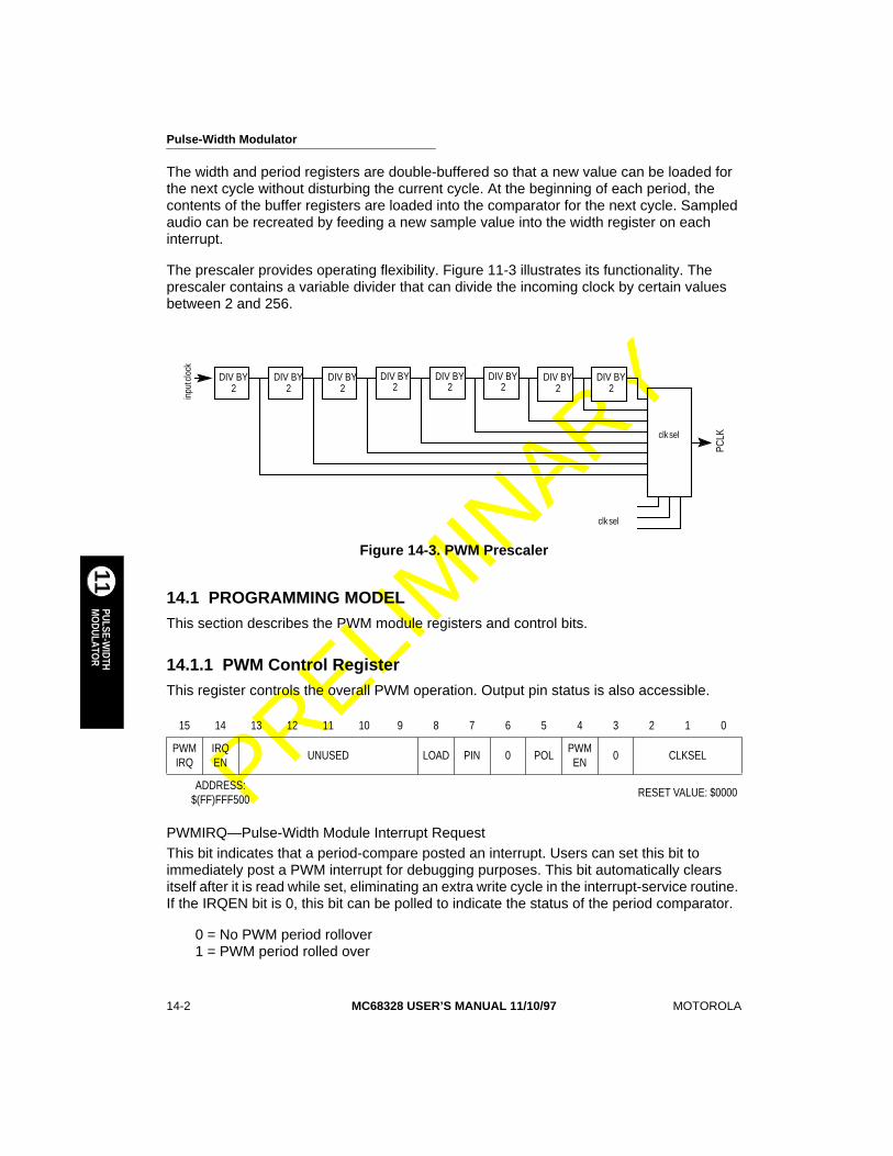
Pulse-Width Modulator
14-2
MC68328 USER’S MANUAL 11/10/97
MOTOROLA
PULSE-WIDTH
11
MO
DULATOR
PRELIM
INARY
The width and period registers are double-buffered so that a new value can be loaded for the next cycle without disturbing the current cycle. At the beginning of each period, the contents of the buffer registers are loaded into the comparator for the next cycle. Sampled audio can be recreated by feeding a new sample value into the width register on each interrupt.
The prescaler provides operating flexibility. Figure 11-3 illustrates its functionality. The prescaler contains a variable divider that can divide the incoming clock by certain values between 2 and 256.
14.1 PROGRAMMING MODEL
This section describes the PWM module registers and control bits.
14.1.1 PWM Control Register
This register controls the overall PWM operation. Output pin status is also accessible.
PWMIRQ—Pulse-Width Module Interrupt RequestThis bit indicates that a period-compare posted an interrupt. Users can set this bit to immediately post a PWM interrupt for debugging purposes. This bit automatically clears itself after it is read while set, eliminating an extra write cycle in the interrupt-service routine. If the IRQEN bit is 0, this bit can be polled to indicate the status of the period comparator.
0 = No PWM period rollover1 = PWM period rolled over
Figure 14-3. PWM Prescaler
15 14 13 12 11 10 9 8 7 6 5 4 3 2 1 0
PWM IRQ
IRQEN
UNUSED LOAD PIN 0 POLPWMEN
0 CLKSEL
ADDRESS: $(FF)FFF500
RESET VALUE: $0000
inpu
t clo
ck
clk sel
clk sel
DIV BY2
DIV BY2
DIV BY2
DIV BY2
DIV BY2
DIV BY2
DIV BY2
DIV BY2
PCLK
Pulse-Width Modulator
MOTOROLA
MC68328 USER’S MANUAL 11/10/97
14-3
PULS
E-W
IDTH
11
MO
DULA
TOR
PRELIM
INARY
IRQEN—Interrupt Request EnableThis bit controls the PWM interrupt. While this bit is low, the interrupt is disabled.
0 = PWM interrupt disabled1 = PWM interrupt enabled
LOAD—LoadThis bit forces a new period. It loads the period and width registers and automatically clears itself after the load has been performed. For slow PCLK periods, the actual load may occur some time after the MPU writes this bit as the load occurs on the next rising PCLK edge.
PIN—PinThis bit indicates the current status of the PWM output pin and can change immediately after it is read, depending on the current state of the pin.
0 = PWM output is low1 = PWM output is high
POL—PolarityThis bit controls the PWM output pin polarity. Normally, the output pin is set high at period boundaries and goes low when a width-compare event occurs.
0 = Normal polarity1 = Inverted polarity
PWMEN—Pulse-Width Module EnableThis bit enables the PWM. While disabled, the PWM is in low-power mode and the prescaler does not count. The output pin is forced to 1 or 0 depending on the setting of the POL bit.
0 = PWM disabled
• The clock prescaler is reset and frozen.
• The counter is reset to 0001 and frozen.
• The contents of the width and period registers are loaded into the comparators.
• The comparators are disabled.
Disabling the PWM may cause a ‘‘glitch’’ on the output, depending on the current state of the counter.
1 = PWM enabled
Pulse-Width Modulator
14-4
MC68328 USER’S MANUAL 11/10/97
MOTOROLA
PULSE-WIDTH
11
MO
DULATOR
PRELIM
INARY
When this bit is set high, the PWM is enabled and begins a new period. The following actions occur:
• The output pin changes state to start a new period.
• The clock prescaler is released and begins counting.
• The counter begins counting.
• The comparators are enabled.
• The IRQ bit is set indicating the start of a new period if IRQEN is set.
CLKSEL—Clock SelectThese bits select the output of the divider chain. The codings are:
000 = Divide by 4 001 = Divide by 8 010 = Divide by 16011 = Divide by 32 100 = Divide by 64 101 = Divide by 128110 = Divide by 256 111 = Divide by 512
14.1.2 Period Register
This register controls the PWM period. When the counter value matches the value in this register, an interrupt is posted and the counter is reset to start another period.
PERIOD—PeriodThis is the value that resets the counter. There is one special case: when this register is $00, the output is never set high (0% duty cycle).
14.1.3 Width Register
This register controls the pulse width. When the counter matches the value in this register, the output is reset for the duration of the period. Note that if the value in this register is higher than the period register, the output will never be reset, resulting in a 100% duty cycle.
WIDTH—WidthWhen the counter reaches the value in this register, the output is reset.
15 14 13 12 11 10 9 8 7 6 5 4 3 2 1 0
PERIOD
ADDRESS: $(FF)FFF502
RESET VALUE: 0000
15 14 13 12 11 10 9 8 7 6 5 4 3 2 1 0
WIDTH
ADDRESS: $(FF)FFF504
RESET VALUE: 0000
Pulse-Width Modulator
MOTOROLA
MC68328 USER’S MANUAL 11/10/97
14-5
PULS
E-W
IDTH
11
MO
DULA
TOR
PRELIM
INARY
14.1.4 Counter
This read-only register is the current count value and can be read at any time without disturbing the counter.
COUNT—CountThis is the current count value.
15 14 13 12 11 10 9 8 7 6 5 4 3 2 1 0
COUNT
ADDRESS: $(FF)FFF506
RESET VALUE: 0000
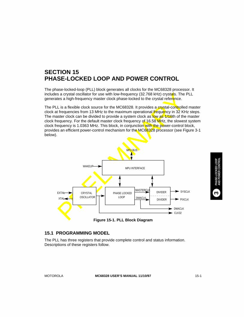
MOTOROLA
MC68328 USER’S MANUAL 11/10/97
15-1
PHAS
E-LO
CKED
LO
OP
3
AND
POW
ER C
ONT
ROL
PRELIM
INARY
SECTION 15PHASE-LOCKED LOOP AND POWER CONTROL
The phase-locked-loop (PLL) block generates all clocks for the MC68328 processor. It includes a crystal oscillator for use with low-frequency (32.768 kHz) crystals. The PLL generates a high-frequency master clock phase-locked to the crystal reference.
The PLL is a flexible clock source for the MC68328. It provides a crystal-controlled master clock at frequencies from 13 MHz to the maximum operational frequency in 32 KHz steps. The master clock can be divided to provide a system clock as low as 1/16th of the master clock frequency. For the default master clock frequency of 16.58 MHz, the slowest system clock frequency is 1.0363 MHz. This block, in conjunction with the power-control block, provides an efficient power-control mechanism for the MC68328 processor (see Figure 3-1 below).
15.1 PROGRAMMING MODEL
The PLL has three registers that provide complete control and status information. Descriptions of these registers follow.
Figure 15-1. PLL Block Diagram
MPU INTERFACE
CRYSTAL
WAKEUP
MPU BUS
OSCILLATORPHASE LOCKED
LOOP
DIVIDER
CLK32
SYSCLKEXTAL
XTAL PIXCLKDMACLK
MASTERCLK
DMACLK
DIVIDER
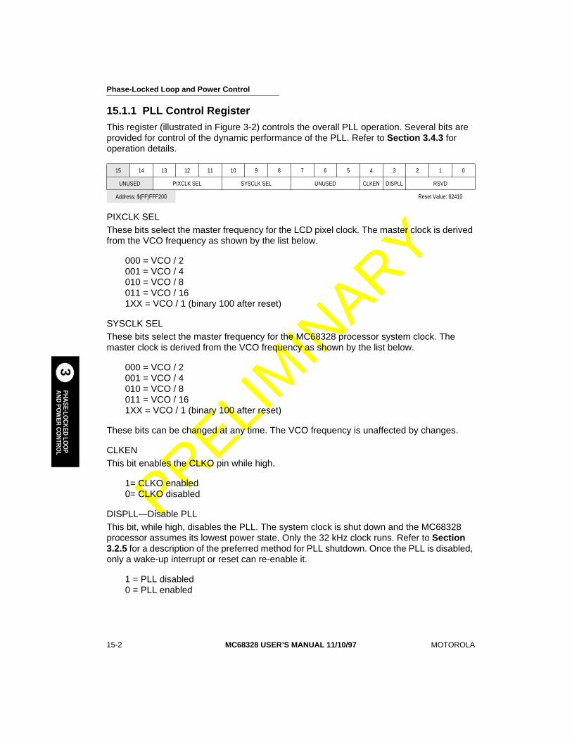
Phase-Locked Loop and Power Control
15-2
MC68328 USER’S MANUAL 11/10/97
MOTOROLA
PHASE-LOCKED LO
OP
3
AND POW
ER CONTRO
L
PRELIM
INARY
15.1.1 PLL Control Register
This register (illustrated in Figure 3-2) controls the overall PLL operation. Several bits are provided for control of the dynamic performance of the PLL. Refer to
Section 3.4.3
for operation details.
PIXCLK SELThese bits select the master frequency for the LCD pixel clock. The master clock is derived from the VCO frequency as shown by the list below.
000 = VCO / 2001 = VCO / 4010 = VCO / 8011 = VCO / 161XX = VCO / 1 (binary 100 after reset)
SYSCLK SELThese bits select the master frequency for the MC68328 processor system clock. The master clock is derived from the VCO frequency as shown by the list below.
000 = VCO / 2001 = VCO / 4010 = VCO / 8011 = VCO / 161XX = VCO / 1 (binary 100 after reset)
These bits can be changed at any time. The VCO frequency is unaffected by changes.
CLKEN This bit enables the CLKO pin while high.
1= CLKO enabled0= CLKO disabled
DISPLL—Disable PLLThis bit, while high, disables the PLL. The system clock is shut down and the MC68328 processor assumes its lowest power state. Only the 32 kHz clock runs. Refer to
Section 3.2.5
for a description of the preferred method for PLL shutdown. Once the PLL is disabled, only a wake-up interrupt or reset can re-enable it.
1 = PLL disabled0 = PLL enabled
15 14 13 12 11 10 9 8 7 6 5 4 3 2 1 0
UNUSED PIXCLK SEL SYSCLK SEL UNUSED CLKEN DISPLL RSVD
Address: $(FF)FFF200 Reset Value: $2410
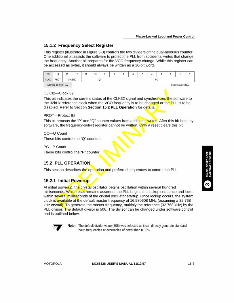
Phase-Locked Loop and Power Control
MOTOROLA
MC68328 USER’S MANUAL 11/10/97
15-3
PHAS
E-LO
CKED
LO
OP
3
AND
POW
ER C
ONT
ROL
PRELIM
INARY
15.1.2 Frequency Select Register
This register (illustrated in Figure 3-3) controls the two dividers of the dual-modulus counter. One additional bit assists the software to protect the PLL from accidental writes that change the frequency. Another bit prepares for the VCO frequency change. While this register can be accessed as bytes, it should always be written as a 16-bit word.
CLK32—Clock 32 This bit indicates the current status of the CLK32 signal and synchronizes the software to the 32kHz reference clock when the VCO frequency is to be changed or the PLL is to be disabled. Refer to Section
Section 15.2 PLL Operation
for details.
PROT—Protect BitThis bit protects the “P” and “Q” counter values from additional writes. After this bit is set by software, the frequency-select register cannot be written. Only a reset clears this bit.
QC—Q CountThese bits control the “Q” counter.
PC—P CountThese bits control the “P” counter.
15.2 PLL OPERATION
This section describes the operation and preferred sequences to control the PLL.
15.2.1 Initial Powerup
At initial powerup, the crystal oscillator begins oscillation within several hundred milliseconds. While reset remains asserted, the PLL begins the lockup sequence and locks within several milliseconds of the crystal oscillator startup. Once lockup occurs, the system clock is available at the default master frequency of 16.580608 MHz (assuming a 32.768 kHz crystal). To generate the master frequency, multiply the reference (32.768 kHz) by the PLL divisor. The default divisor is 506. The divisor can be changed under software control and is outlined below.
15 14 13 12 11 10 9 8 7 6 5 4 3 2 1 0
CLK32 PROT UNUSED QC PC
Address: $(FF)FFF202 Reset Value: $0123
Note:
The default divider value (506) was selected as it can directly generate standardbaud frequencies at accuracies of better than 0.05%.
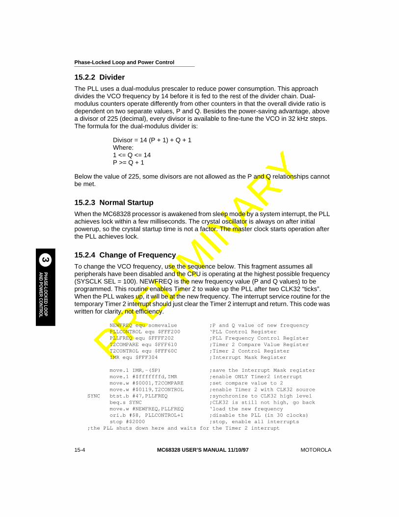
Phase-Locked Loop and Power Control
15-4
MC68328 USER’S MANUAL 11/10/97
MOTOROLA
PHASE-LOCKED LO
OP
3
AND POW
ER CONTRO
L
PRELIM
INARY
15.2.2 Divider
The PLL uses a dual-modulus prescaler to reduce power consumption. This approach divides the VCO frequency by 14 before it is fed to the rest of the divider chain. Dual-modulus counters operate differently from other counters in that the overall divide ratio is dependent on two separate values, P and Q. Besides the power-saving advantage, above a divisor of 225 (decimal), every divisor is available to fine-tune the VCO in 32 kHz steps. The formula for the dual-modulus divider is:
Divisor = 14 (P + 1) + Q + 1Where:1 <= Q <= 14P >= Q + 1
Below the value of 225, some divisors are not allowed as the P and Q relationships cannot be met.
15.2.3 Normal Startup
When the MC68328 processor is awakened from sleep mode by a system interrupt, the PLL achieves lock within a few milliseconds. The crystal oscillator is always on after initial powerup, so the crystal startup time is not a factor. The master clock starts operation after the PLL achieves lock.
15.2.4 Change of Frequency
To change the VCO frequency, use the sequence below. This fragment assumes all peripherals have been disabled and the CPU is operating at the highest possible frequency (SYSCLK SEL = 100). NEWFREQ is the new frequency value (P and Q values) to be programmed. This routine enables Timer 2 to wake up the PLL after two CLK32 “ticks”. When the PLL wakes up, it will be at the new frequency. The interrupt service routine for the temporary Timer 2 interrupt should just clear the Timer 2 interrupt and return. This code was written for clarity, not efficiency.
NEWFREQ equ somevalue ;P and Q value of new frequencyPLLCONTROL equ $FFF200 ‘PLL Control RegisterPLLFREQ equ $FFFF202 ;PLL Frequency Control RegisterT2COMPARE equ $FFF610 ;Timer 2 Compare Value RegisterT2CONTROL equ $FFF60C ;Timer 2 Control RegisterIMR equ $FFF304 ;Interrupt Mask Register
move.1 IMR,-(SP) ;save the Interrupt Mask registermove.1 #$fffffffd,IMR ;enable ONLY Timer2 interruptmove.w #$0001,T2COMPARE ;set compare value to 2move.w #$0119,T2CONTROL ;enable Timer 2 with CLK32 source
SYNC btst.b #47,PLLFREQ ;synchronize to CLK32 high levelbeq.s SYNC ;CLK32 is still not high, go backmove.w #NEWFREQ,PLLFREQ ‘load the new frequencyori.b #$8, PLLCONTROL+1 ;disable the PLL (in 30 clocks)stop #$2000 ;stop, enable all interrupts
;the PLL shuts down here and waits for the Timer 2 interrupt
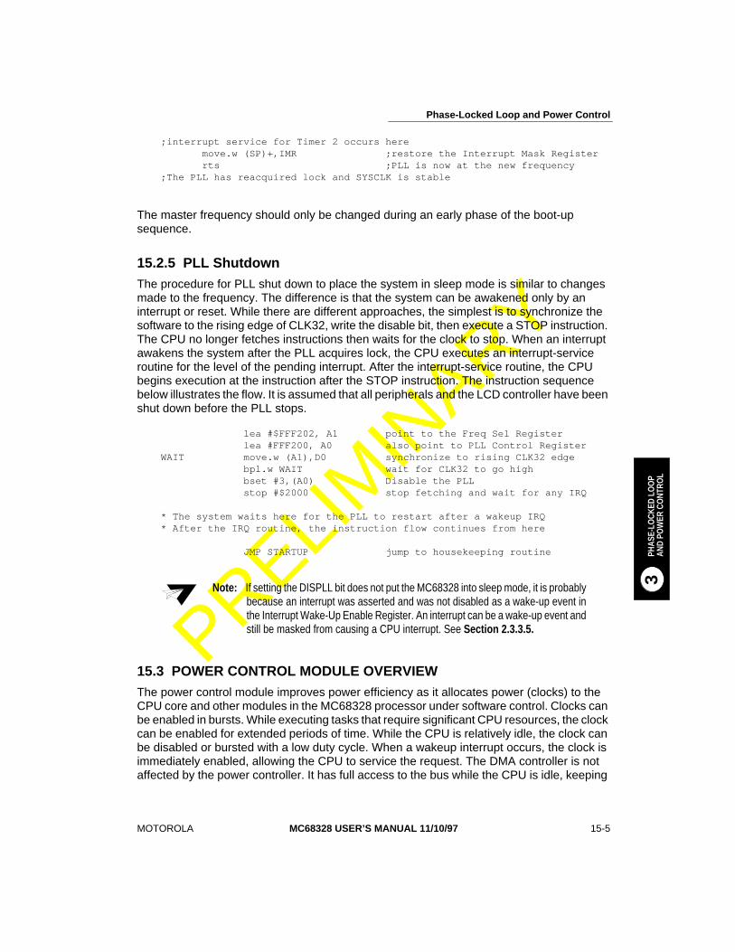
Phase-Locked Loop and Power Control
MOTOROLA
MC68328 USER’S MANUAL 11/10/97
15-5
PHAS
E-LO
CKED
LO
OP
3
AND
POW
ER C
ONT
ROL
PRELIM
INARY
;interrupt service for Timer 2 occurs heremove.w (SP)+,IMR ;restore the Interrupt Mask Registerrts ;PLL is now at the new frequency
;The PLL has reacquired lock and SYSCLK is stable
The master frequency should only be changed during an early phase of the boot-up sequence.
15.2.5 PLL Shutdown
The procedure for PLL shut down to place the system in sleep mode is similar to changes made to the frequency. The difference is that the system can be awakened only by an interrupt or reset. While there are different approaches, the simplest is to synchronize the software to the rising edge of CLK32, write the disable bit, then execute a STOP instruction. The CPU no longer fetches instructions then waits for the clock to stop. When an interrupt awakens the system after the PLL acquires lock, the CPU executes an interrupt-service routine for the level of the pending interrupt. After the interrupt-service routine, the CPU begins execution at the instruction after the STOP instruction. The instruction sequence below illustrates the flow. It is assumed that all peripherals and the LCD controller have been shut down before the PLL stops.
lea #$FFF202, A1 point to the Freq Sel Registerlea #FFF200, A0 also point to PLL Control Register
WAIT move.w (A1),D0 synchronize to rising CLK32 edgebpl.w WAIT wait for CLK32 to go highbset #3,(A0) Disable the PLLstop #$2000 stop fetching and wait for any IRQ
* The system waits here for the PLL to restart after a wakeup IRQ* After the IRQ routine, the instruction flow continues from here
JMP STARTUP jump to housekeeping routine
15.3 POWER CONTROL MODULE OVERVIEW
The power control module improves power efficiency as it allocates power (clocks) to the CPU core and other modules in the MC68328 processor under software control. Clocks can be enabled in bursts. While executing tasks that require significant CPU resources, the clock can be enabled for extended periods of time. While the CPU is relatively idle, the clock can be disabled or bursted with a low duty cycle. When a wakeup interrupt occurs, the clock is immediately enabled, allowing the CPU to service the request. The DMA controller is not affected by the power controller. It has full access to the bus while the CPU is idle, keeping
Note:
If setting the DISPLL bit does not put the MC68328 into sleep mode, it is probablybecause an interrupt was asserted and was not disabled as a wake-up event inthe Interrupt Wake-Up Enable Register. An interrupt can be a wake-up event andstill be masked from causing a CPU interrupt. See
Section 2.3.3.5.
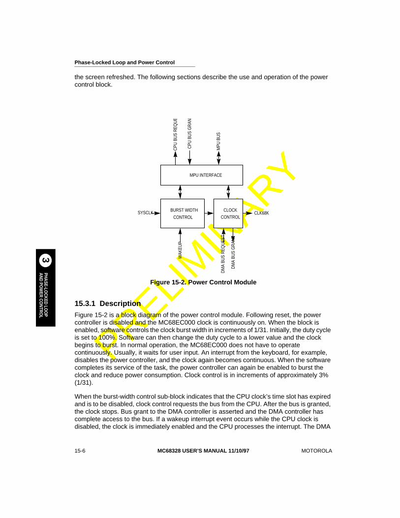
Phase-Locked Loop and Power Control
15-6
MC68328 USER’S MANUAL 11/10/97
MOTOROLA
PHASE-LOCKED LO
OP
3
AND POW
ER CONTRO
L
PRELIM
INARY
the screen refreshed. The following sections describe the use and operation of the power control block.
15.3.1 Description
Figure 15-2 is a block diagram of the power control module. Following reset, the power controller is disabled and the MC68EC000 clock is continuously on. When the block is enabled, software controls the clock burst width in increments of 1/31. Initially, the duty cycle is set to 100%. Software can then change the duty cycle to a lower value and the clock begins to burst. In normal operation, the MC68EC000 does not have to operate continuously. Usually, it waits for user input. An interrupt from the keyboard, for example, disables the power controller, and the clock again becomes continuous. When the software completes its service of the task, the power controller can again be enabled to burst the clock and reduce power consumption. Clock control is in increments of approximately 3% (1/31).
When the burst-width control sub-block indicates that the CPU clock’s time slot has expired and is to be disabled, clock control requests the bus from the CPU. After the bus is granted, the clock stops. Bus grant to the DMA controller is asserted and the DMA controller has complete access to the bus. If a wakeup interrupt event occurs while the CPU clock is disabled, the clock is immediately enabled and the CPU processes the interrupt. The DMA
Figure 15-2. Power Control Module
MPU INTERFACE
BURST WIDTH
CONTROL
CLOCKCONTROL
SYSCLK
WAK
EUP
MPU
BU
SCLK68K
DM
A BU
S R
EQU
EST
DM
A BU
S G
RAN
T
CPU
BU
S R
EQU
E
CPU
BU
S G
RAN
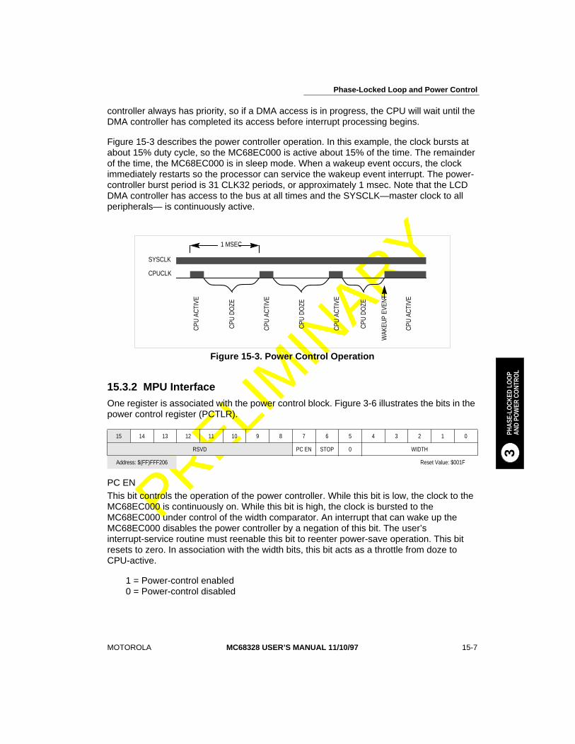
Phase-Locked Loop and Power Control
MOTOROLA
MC68328 USER’S MANUAL 11/10/97
15-7
PHAS
E-LO
CKED
LO
OP
3
AND
POW
ER C
ONT
ROL
PRELIM
INARY
controller always has priority, so if a DMA access is in progress, the CPU will wait until the DMA controller has completed its access before interrupt processing begins.
Figure 15-3 describes the power controller operation. In this example, the clock bursts at about 15% duty cycle, so the MC68EC000 is active about 15% of the time. The remainder of the time, the MC68EC000 is in sleep mode. When a wakeup event occurs, the clock immediately restarts so the processor can service the wakeup event interrupt. The power-controller burst period is 31 CLK32 periods, or approximately 1 msec. Note that the LCD DMA controller has access to the bus at all times and the SYSCLK—master clock to all peripherals— is continuously active.
15.3.2 MPU Interface
One register is associated with the power control block. Figure 3-6 illustrates the bits in the power control register (PCTLR).
PC ENThis bit controls the operation of the power controller. While this bit is low, the clock to the MC68EC000 is continuously on. While this bit is high, the clock is bursted to the MC68EC000 under control of the width comparator. An interrupt that can wake up the MC68EC000 disables the power controller by a negation of this bit. The user’s interrupt-service routine must reenable this bit to reenter power-save operation. This bit resets to zero. In association with the width bits, this bit acts as a throttle from doze to CPU-active.
1 = Power-control enabled0 = Power-control disabled
Figure 15-3. Power Control Operation
15 14 13 12 11 10 9 8 7 6 5 4 3 2 1 0
RSVD PC EN STOP 0 WIDTH
Address: $(FF)FFF206 Reset Value: $001F
SYSCLK
CPUCLK
WAK
EUP
EVEN
T
CPU
DO
ZE
CPU
AC
TIVE
CPU
AC
TIVE
CPU
AC
TIVE
CPU
AC
TIVE
CPU
DO
ZE
CPU
DO
ZE
1 MSEC
Phase-Locked Loop and Power Control
15-8
MC68328 USER’S MANUAL 11/10/97
MOTOROLA
PHASE-LOCKED LO
OP
3
AND POW
ER CONTRO
L
PRELIM
INARY
STOPThis bit immediately enters the power-save mode without waiting for the power controller to cycle through a complete burst period. This bit disables the CPU clock after the bus cycle that follows the next CLK32 rising edge. When the system is to enter the doze mode, this bit is set. On the next burst period, or interrupt, the clock will restart for its allotted period. This bit is reset to zero and is cleared on wake-up events.
1 = Stop CPU clock (enter doze mode)0 = Normal CPU clock bursts
WIDTHWidth of CPU clock bursts. These bits reset to 11111 ($1F).
00000 = 0/31 duty cycle00001 = 1/31 duty cycle00010 = 2/31 duty cycle
...11111 = 31/31 duty cycle
These bits control the width of the CPU clock bursts in 1/31 increments. While the WIDTH is 1 and the power controller is enabled, the clock is bursted to the CPU at a duty cycle of 1/31. While the WIDTH bits are 1F(hex), the clock is always on. While the WIDTH is zero, the clock is always off. Set the WIDTH to 0 when the CPU should be disabled for extended time periods, but it can be awakened without waiting for the PLL to re-acquire lock.
These bits are not affected by clearing the PC EN bit. When an interrupt disables the power controller, these bits are not changed. Users should enter the doze mode by setting the PCEN or STOP bit after an interrupt has been serviced. Typically, it is the STOP bit that is set.
15.3.3 Operation
This section describes how to use the variable duty-cycle or STOP bit in the power controller to enter doze mode.
15.3.3.1 NORMAL OPERATION
When the MC68328 processor begins operation after reset, the power controller is disabled and the MC68EC000 internal clock runs continuously. To reduce the power consumed by the MC68EC000, the power controller is enabled when the STOP or PCEN bit is set. The value in the WIDTH register determines the duty cycle of the clock-bursts that are applied to the MC68EC000 when PCEN is set. If an interrupt is received, the power controller is automatically disabled. It is up to the interrupt-service routine to re-enable the power controller.
Phase-Locked Loop and Power Control
MOTOROLA
MC68328 USER’S MANUAL 11/10/97
15-9
PHAS
E-LO
CKED
LO
OP
3
AND
POW
ER C
ONT
ROL
PRELIM
INARY
The CLKO pin is an external reference of the internal MC68EC000 clock. If the external system does not require CLKO, it can be disabled by clearing the CLKEN bit in the PLL control register further reducing the normal operation power consumption.
15.3.3.2 DOZE OPERATION
The MC68EC000 clock can be disabled for extended periods by setting the STOP bit or WIDTH register bits to 00000 and setting the PC EN bit to 1. The MC68EC000 clock is enabled again when it receives an interrupt. At the end of the service routine, the power controller can be re-enabled, putting the MC68EC000 back into DOZE mode. Once the MC68EC000 clock is disabled, only an interrupt or hardware reset can re-enable it.
Users can program the duty-cycle register (WIDTH bits) for burst-duty cycles of any value between 0/31 and 31/31. This effectively provides a variable clock frequency (and power dissipation) of between 0% and 100% of the system clock frequency in 3% incremental steps. However, by setting the STOP bit, most applications will consume the least amount of power by entering doze mode whenever possible.
While in DOZE mode, the port I/O pins remain in the state prior to entering DOZE mode. CLKO may still be active while the processor core is in DOZE mode. For lowest power operation, CLKO should be disabled. CLKO is controlled by the CLKEN bit of the PLL control register. The data bus is pulled up by internal pullup resistors while the MC68EC000 core is in DOZE mode and the LCDC is not using the data bus to load screen refresh data.
15.3.3.3 SLEEP OPERATION
The PLL is disabled in the SLEEP mode. Only the 32 kHz clock continuously operates to keep the real-time clock operational. Wakeup events can activate the PLL and the system clock will begin to operate within 2 msec. SLEEP mode is entered by setting the DISPLL bit in the PLL Control Register. See
Section 3.2.5
for more information.
While in SLEEP mode, the port I/O pins remain in the state prior to entering SLEEP mode. CLKO will not be active while the processor core is in SLEEP. The data bus is pulled up by internal pullup resistors while the PLL is disabled. To maintain reliable edges on CLKO, it is a good practice to disable CLKO before entering SLEEP mode and re-enable CLK0 after wake-up.
MOTOROLA
MC68328 USER’S MANUAL 11/10/97
16-1
APPL
ICAT
IONS
AND
14
DESI
GN
EXAM
PLES
PRELIM
INARY
SECTION 16APPLICATIONS AND DESIGN EXAMPLES
This section discusses the details of a simple M68328 processor base system, which will illustrate the simplicity of the system hardware design and glueless interface to various memory and peripheral devices when using the M68328 processor. The ability of a mixed 8-bit and 16-bit memory is also demonstrated. This system consists of:
• M68328 16.58MHz (using 32.768kHz crystal)
• 512K boot EPROM x 1 (8-bit interface)
• 2M general-purpose EPROM (16-bit interface)
• 512K SRAM (8-bit interface)
• 2M general-purpose SRAM (16-bit interface)
16.1 MEMORY MAP
The M68328 processor can support up to 4G address space. This example uses an address space under 16M for simplicity.
Figure 16-1. Memory Map
2.5MB SRAM
2.5MB EPROM
PCMCIA 1.0 CARD4MB SPACE
UNUSED
$00000000 - $003FFFFF
$00400000 - $007FFFFF
$00FFF000 - $00FFFFFF
$00800000 - $00BFFFFF
68328 INTERNALREGISTERS
CSB0, CSB1, CSB2
CSA0, CSA1, CSA2
Applications and Design Examples
16-2
MC68328 USER’S MANUAL 11/10/97
MOTOROLA
APPLICATIONS AND
14
DESIGN EXAM
PLES
PRELIM
INARY
16.1.1 M68328 Processor Signal Configuration
A low boot bus width-select (BBUSW) at reset means that the system will boot up with an 8-bit ROM. A low mode-clock (MOCLK) signal at reset means that the M68328 processor uses the 32.768kHz crystal and enables its internal PLL to supply the clock for the entire chip. The suggested circuit for PLL is shown in Figure 14-2. The RESET signal should be connected to the JTAGRST signal to ensure that the entire chip (including the JTAG block) is reset properly at the same time. The RESET and JTAGRST should be held low for more than 100ms before they are released as required by the M68EC000 user’s manual. There is no power-on-reset circuit implemented in the M68328 processor; therefore, use external circuits (either from a MC1455 mono-stable timer or power-on-reset signal from most of the power supply chips) to generate the RESET signal. The RESET signal in this example connects to a debouncing circuit to generate a reset for the M68328 processor.
Figure 16-2. M68328 Processor Signal Configuration
To Power SupplyPLLVCC
RESET
MC68328
XTAL EXTAL
16.67MHZ
32.768kHz
20pF20pF
PLLGND
VCC’s
GND’sTo Power Supply
IRQ7
10K
10K
10K
10K
VCC
VCC
VCC
VCC
JTAGRST
TDITDOTMSTCK
10K
VCC
10K
VCC
10K
VCC
BBUSW
MOCLK
RESET
ABORT
.luf
Applications and Design Examples
MOTOROLA
MC68328 USER’S MANUAL 11/10/97
16-3
APPL
ICAT
IONS
AND
14
DESI
GN
EXAM
PLES
PRELIM
INARY
The PLLVCC and PLLGND pins should have a .luf bypass capacitor as close to them as possible to reduce the noise induced into the PLL clock synthesis circuit. In general, PLLVCC and PLLGND can be connected to the main power supply with adequate filtering. Bypass capacitors for normal VCC and GND pins are also recommended. Because JTAG is not used in general operations, those related signals (TDI, TMS, and TCK) should be pulled high through resistors to avoid unknown states. The IRQ7 connects to a debouncing circuit in this example to generate a Level 7 interrupt of the M68328 processor when the ABORT button is activated.
16.1.2 Memory Interface
16.1.2.1 EPROM INTERFACE
The M68328 processor supports both 8-bit and 16-bit devices. Any chip-select can be individually programmed for 8 or 16 bits; however, CSA0 can be programmed only by the externally supplied BBUSW signal. Figure 14-3 shows the connection of M68328 processor to EPROM. The OE signal controls the EPROM output-enable. When the M68328 processor performs a read cycle (8-bit or 16-bit), the OE signal will always be asserted. CSA0 is connected to the CE signal of the boot EPROM and the CSA1 and CSA2 are connected to the CE signals of the other EPROMs. To achieve better (faster) timing, users can tie the EPROM CE signal to GND and hook the CSAx signal to the EPROM OE signal. However,
this is not recommended in a power-conscious system because the EPROM will be on all the time
.
16.1.2.2 SRAM INTERFACE
The M68328 processor provides internally decoded write-enable signals, LWE and UWE, for a glueless interface to SRAM. They are connected to the write-enable (W) signals of the 16-bit (8-bit x 2) SRAM. The OE signal is also used to gate the output signal from the SRAM during a write cycle that is connected to the SRAM G signal. CSB0 is connected to the E signal. The 8-bit SRAM can also be mixed with 16-bit SRAM. For 8-bit-oriented SRAM, only the UWE is used for the W signal.
Note:
PLLVCC must always operate at 3.3V, even when using the 5V MC68328version.
Note:
The WE signal of the M68328 processor supports PCMCIA 1.0 (when CSD3 isin use). It cannot be used for general SRAM write-enable signals.
Applications and Design Examples
16-4
MC68328 USER’S MANUAL 11/10/97
MOTOROLA
APPLICATIONS AND
14
DESIGN EXAM
PLES
PRELIM
INARY
Figure 16-3. EPROM Interface
D013D0
D114D1
D215D2
D317D3
D418D4
D519D5
D620D6
D721D7
A0A1A2A3A4A5A6A7A8A9
A10A11A12A13A14A15A16A17A18
A1A2A3A4A5A6A7A8A9
A10A11A12A13A14A15A16A17A18A19
121110987652726232542829323031
CE22CSA1
OE24OE
27C040512KX8EPROM
D013D8
D114D9
D215D10
D317D11
D418D12
D519D13
D620D14
D721D15
A0A1A2A3A4A5A6A7A8A9
A10A11A12A13A14A15A16A17A18
A1A2A3A4A5A6A7A8A9
A10A11A12A13A14A15A16A17A18A19
121110987652726232542829323031
CE22CSA1
OE24OE
27C040512KX8EPROM
D013D0
D114D1
D215D2
D317D3
D418D4
D519D5
D620D6
D721D7
A0A1A2A3A4A5A6A7A8A9
A10A11A12A13A14A15A16A17A18
A1A2A3A4A5A6A7A8A9
A10A11A12A13A14A15A16A17A18A19
121110987652726232542829323031
CE22CSA2
OE24OE
27C040512KX8EPROM
D013D8
D114D9
D215D10
D317D11
D418D12
D519D13
D620D14
D721D15
A0A1A2A3A4A5A6A7A8A9
A10A11A12A13A14A15A16A17A18
A1A2A3A4A5A6A7A8A9
A10A11A12A13A14A15A16A17A18A19
121110987652726232542829323031
CE22CSA2
OE24OE
27C040512KX8EPROM
D013D8
D114D9
D215D10
D317D11
D418D12
D519D13
D620D14
D721D15
A0A1A2A3A4A5A6A7A8A9
A10A11A12A13A14A15A16A17A18
121110987652726232542829323031
CE22CSA0
OE24OE
27C040512KX8EPROM
A0A1A2A3A4A5A6A7A8A9
A10A11A12A13A14A15A16A17A18
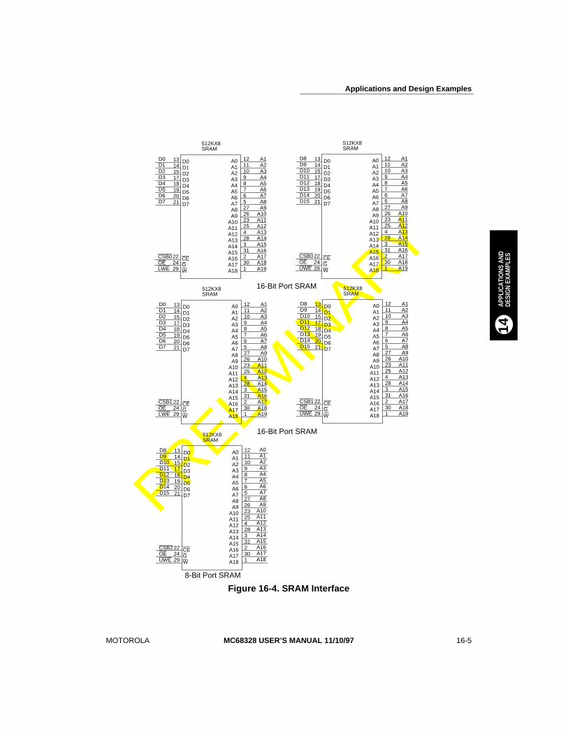
Applications and Design Examples
MOTOROLA
MC68328 USER’S MANUAL 11/10/97
16-5
APPL
ICAT
IONS
AND
14
DESI
GN
EXAM
PLES
PRELIM
INARY
Figure 16-4. SRAM Interface
D013D0
D114D1
D215D2
D317D3
D418D4
D519D5
D620D6
D721D7
A0A1A2A3A4A5A6A7A8A9
A10A11A12A13A14A15A16A17A18
A1A2A3A4A5A6A7A8A9
A10A11A12A13A14A15A16A17A18A19
12111098765272623254283312301
CE22CSB0
G24OE
W29LWE
512KX8SRAM
D013D8
D114D9
D215D10
D317D11
D418D12
D519D13
D620D14
D721D15
A0A1A2A3A4A5A6A7A8A9
A10A11A12A13A14A15A16A17A18
A1A2A3A4A5A6A7A8A9
A10A11A12A13A14A15A16A17A18A19
12111098765272623254283312301
CE22CSB0
G24OE
W29UWE
512KX8SRAM
D013D0
D114D1
D215D2
D317D3
D418D4
D519D5
D620D6
D721D7
A0A1A2A3A4A5A6A7A8A9
A10A11A12A13A14A15A16A17A18
A1A2A3A4A5A6A7A8A9
A10A11A12A13A14A15A16A17A18A19
12111098765272623254283312301
CE22CSB1
G24OE
W29LWE
512KX8SRAM
D013D8
D114D9
D215D10
D317D11
D418D12
D519D13
D620D14
D721D15
A0A1A2A3A4A5A6A7A8A9
A10A11A12A13A14A15A16A17A18
A1A2A3A4A5A6A7A8A9
A10A11A12A13A14A15A16A17A18A19
12111098765272623254283312301
CE22CSB1
G24OE
W29UWE
512KX8SRAM
D013D8
D114D9
D215D10
D317D11
D418D12
D519D13
D620D14
D721D15
A0A1A2A3A4A5A6A7A8A9
A10A11A12A13A14A15A16A17A18
12111098765272623254283312301
CE22CSB2
G24OE
W29UWE
512KX8SRAM
A0A1A2A3A4A5A6A7A8A9
A10A11A12A13A14A15A16A17A18
8-Bit Port SRAM
16-Bit Port SRAM
16-Bit Port SRAM
Applications and Design Examples
16-6
MC68328 USER’S MANUAL 11/10/97
MOTOROLA
APPLICATIONS AND
14
DESIGN EXAM
PLES
PRELIM
INARY
16.2 SYSTEM INITIALIZATION EXAMPLES
16.2.1 Software Listing 1 - Initialization Code
M328BASE equ $FFF000 ; SIM28 System Configuration Registers SCR equ (M328BASE+$000) ; Chip Select Registers
; CS Group Base Registers GRPBASEA equ (M328BASE+$100)GRPBASEB equ (M328BASE+$102)GRPBASEC equ (M328BASE+$104)GRPBASED equ (M328BASE+$106)
; CS Group Mask Registers GRPMASKA equ (M328BASE+$108)GRPMASKB equ (M328BASE+$10A)GRPMASKC equ (M328BASE+$10C)GRPMASKD equ (M328BASE+$10E)
; Group A CS Registers CSA0 equ (M328BASE+$110)CSA1 equ (M328BASE+$114)CSA2 equ (M328BASE+$118)CSA3 equ (M328BASE+$11C)
; Group B CS Registers CSB0 equ (M328BASE+$120)CSB1 equ (M328BASE+$124)CSB2 equ (M328BASE+$128)CSB3 equ (M328BASE+$12C)
; Group C CS Registers CSC0 equ (M328BASE+$130)CSC1 equ (M328BASE+$134)CSC2 equ (M328BASE+$138)CSC3 equ (M328BASE+$13C)
; Group D CS Registers CSD0 equ (M328BASE+$140)CSD1 equ (M328BASE+$144)CSD2 equ (M328BASE+$148)CSD3 equ (M328BASE+$14C) ; PLL Registers PLLCR equ (M328BASE+$200); Control Reg PLLFSR equ (M328BASE+$202); Freq Select Reg PLLTSR equ (M328BASE+$204); Test Reg ; Power Control Registers PCTLR equ (M328BASE+$206); Control Reg ; Interrupt Registers IVR equ (M328BASE+$300); Interrupt Vector Reg ICR equ (M328BASE+$302); Interrupt Control Reg IMR equ (M328BASE+$304); Interrupt Mask Reg IWR equ (M328BASE+$308); Wakeup Enable Reg ISR equ (M328BASE+$30C); Interrupt Status Reg IPR equ (M328BASE+$310); Interrupt Pending Reg ; PIO Registers
; Port A Registers
Applications and Design Examples
MOTOROLA
MC68328 USER’S MANUAL 11/10/97
16-7
APPL
ICAT
IONS
AND
14
DESI
GN
EXAM
PLES
PRELIM
INARY
PADIR equ (M328BASE+$400); Direction Reg PADATA equ (M328BASE+$401); Data Reg PASEL equ (M328BASE+$403); Select Reg
; Port B Registers PBDIR equ (M328BASE+$408); Direction Reg PBDATA equ (M328BASE+$409); Data Reg PBSEL equ (M328BASE+$40B); Select Reg
; Port C Registers PCDIR equ (M328BASE+$410); Direction Reg PCDATA equ (M328BASE+$411); Data Reg PCSEL equ (M328BASE+$413); Select Reg
; Port D Registers PDDIR equ (M328BASE+$418); Direction Reg PDDATA equ (M328BASE+$419); Data Reg PDPUEN equ (M328BASE+$41A); Pullup Enable Reg PDPOL equ (M328BASE+$41C); Polarity Reg PDIRQEN equ (M328BASE+$41D); IRQ Enable Reg PDIRQEDGE equ (M328BASE+$41F); IRQ Edge Reg
; Port E Registers PEDIR equ (M328BASE+$420); Direction Reg PEDATA equ (M328BASE+$421); Data Reg PESEL equ (M328BASE+$423); Select Reg
; Port F Registers PFDIR equ (M328BASE+$428); Direction Reg PFDATA equ (M328BASE+$429); Data Reg PFSEL equ (M328BASE+$42B); Select Reg
; Port G Registers PGDIR equ (M328BASE+$430); Direction Reg PGDATA equ (M328BASE+$431); Data Reg PGSEL equ (M328BASE+$433); Select Reg
; Port J Registers PJDIR equ (M328BASE+$438); Direction Reg PJDATA equ (M328BASE+$439); Data Reg PJSEL equ (M328BASE+$43B); Select Reg
; Port K Registers PKDIR equ (M328BASE+$440); Direction Reg PKDATA equ (M328BASE+$441); Data Reg PKSEL equ (M328BASE+$443); Select Reg
; Port M Registers PMDIR equ (M328BASE+$448); Direction Reg PMDATA equ (M328BASE+$449); Data Reg PMPUEN equ (M328BASE+$44A); Pullup Enable Reg PMSEL equ (M328BASE+$44B); Select Reg ; PWM Registers PWMC equ (M328BASE+$500); Control Reg PWMP equ (M328BASE+$502); Period Reg PWMW equ (M328BASE+$504); Width Reg PWMCNT equ (M328BASE+$506); Counter ; Timer Registers
; Timer 1 Registers TCTL1 equ (M328BASE+$600); Control Reg TPRER1 equ (M328BASE+$602); Prescalar Reg TCMP1 equ (M328BASE+$604); Compare Reg TCR1 equ (M328BASE+$606); Capture Reg TCN1 equ (M328BASE+$608); Counter TSTAT1 equ (M328BASE+$60A); Status Reg
; Timer 2 Registers TCTL2 equ (M328BASE+$60C); Control Reg TPRER2 equ (M328BASE+$60E); Prescalar Reg
Applications and Design Examples
16-8
MC68328 USER’S MANUAL 11/10/97
MOTOROLA
APPLICATIONS AND
14
DESIGN EXAM
PLES
PRELIM
INARY
TCMP2 equ (M328BASE+$610); Compare Reg TCR2 equ (M328BASE+$612); Capture Reg TCN2 equ (M328BASE+$614); Counter TSTAT2 equ (M328BASE+$616); Status Reg ; Watchdog Registers WCR equ (M328BASE+$618); Control Reg WRR equ (M328BASE+$61A); Reference Reg WCN equ (M328BASE+$61C); Counter ; SPI Registers
; SPI Slave Registers SPISR equ (M328BASE+$700); SPIS Reg
;SPI Master Registers SPIMDATA equ (M328BASE+$800); Control/Status Reg SPIMCONT equ (M328BASE+$802); Data Reg ; UART Registers USTCNT equ (M328BASE+$900); Status Control Reg UBAUD equ (M328BASE+$902); Baud Control Reg UARTRX equ (M328BASE+$904); Rx Reg UARTTX equ (M328BASE+$906); Tx Reg UARTMISC equ (M328BASE+$908); Misc Reg ; LCDC Registers LSSA equ (M328BASE+$A00); Screen Start Addr Reg LVPW equ (M328BASE+$A05); Virtual Page Width Reg LXMAX equ (M328BASE+$A08); Screen Width Reg LYMAX equ (M328BASE+$A0A); Screen Height Reg LCXP equ (M328BASE+$A18); Cursor X Position LCYP equ (M328BASE+$A1A); Cursor Y Position LCWCH equ (M328BASE+$A1C); Cursor Width & Height Reg LBLKC equ (M328BASE+$A1F); Blink Control Reg LPICF equ (M328BASE+$A20); Panel Interface Config Reg LPOLCF equ (M328BASE+$A21); Polarity Config Reg LACDRC equ (M328BASE+$A23); ACD (M) Rate Control Reg LPXCD equ (M328BASE+$A25); Pixel Clock Divider Reg LCKCON equ (M328BASE+$A27); Clocking Control Reg LLBAR equ (M328BASE+$A29); Last Buffer Addr Reg LOTCR equ (M328BASE+$A2B); Octet Terminal Count Reg LPOSR equ (M328BASE+$A2D); Panning Offset Reg LFRCM equ (M328BASE+$A31); Frame Rate Control Mod Reg LGPMR equ (M328BASE+$A32); Gray Palette Mapping Reg LIRQR equ (M328BASE+$A34); Interrupt Control Reg ; RTC Registers RTCHMSR equ (M328BASE+$B00); Hrs Mins Secs Reg RTCALM0R equ (M328BASE+$B04); Alarm Register 0 RTCALM1R equ (M328BASE+$B08); Alarm Register 1 RTCCTL equ (M328BASE+$B0C); Control Reg RTCISR equ (M328BASE+$B0E); Interrupt Status Reg RTCIENR equ (M328BASE+$B10); Interrupt Enable Reg RSTPWCH equ (M328BASE+$B12) ; Stopwatch Minutes Reset_start: move.w #$2700,sr ; mask off all interrupts;**********************************************************************;; Initialize I/O according to user’s configuration;
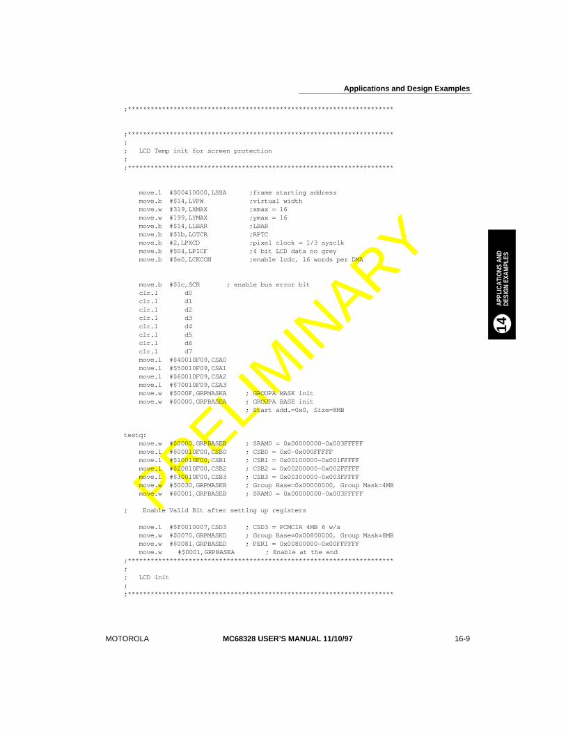
Applications and Design Examples
MOTOROLA
MC68328 USER’S MANUAL 11/10/97
16-9
APPL
ICAT
IONS
AND
14
DESI
GN
EXAM
PLES
PRELIM
INARY
;**********************************************************************
;**********************************************************************;; LCD Temp init for screen protection;;********************************************************************** move.l #$00410000,LSSA ;frame starting address move.b #$14,LVPW ;virtual width move.w #319,LXMAX ;xmax = 16 move.w #199,LYMAX ;ymax = 16 move.b #$14,LLBAR ;LBAR move.b #$1b,LOTCR ;RPTC move.b #2,LPXCD ;pixel clock = 1/3 sysclk move.b #$04,LPICF ;4 bit LCD data no grey move.b #$e0,LCKCON ;enable lcdc, 16 words per DMA
move.b #$1c,SCR ; enable bus error bit clr.l d0 clr.l d1 clr.l d2 clr.l d3 clr.l d4 clr.l d5 clr.l d6 clr.l d7 move.l #$40010F09,CSA0 move.l #$50010F09,CSA1 move.l #$60010F09,CSA2 move.l #$70010F09,CSA3 move.w #$000F,GRPMASKA ; GROUPA MASK init move.w #$0000,GRPBASEA ; GROUPA BASE init ; Start add.=0x0, Size=8MB
testq: move.w #$0000,GRPBASEB ; SRAM0 = 0x00000000-0x003FFFFF move.l #$00010F00,CSB0 ; CSB0 = 0x0-0x000FFFFF move.l #$10010F00,CSB1 ; CSB1 = 0x00100000-0x001FFFFF move.l #$20010F00,CSB2 ; CSB2 = 0x00200000-0x002FFFFF move.l #$30010F00,CSB3 ; CSB3 = 0x00300000-0x003FFFFF move.w #$0030,GRPMASKB ; Group Base=0x00000000, Group Mask=4MB move.w #$0001,GRPBASEB ; SRAM0 = 0x00000000-0x003FFFFF
; Enable Valid Bit after setting up registers move.l #$f0010007,CSD3 ; CSD3 = PCMCIA 4MB 6 w/s move.w #$0070,GRPMASKD ; Group Base=0x00800000, Group Mask=8MB move.w #$0081,GRPBASED ; PERI = 0x00800000-0x00FFFFFF move.w #$0001,GRPBASEA ; Enable at the end;**********************************************************************;; LCD init ;;**********************************************************************
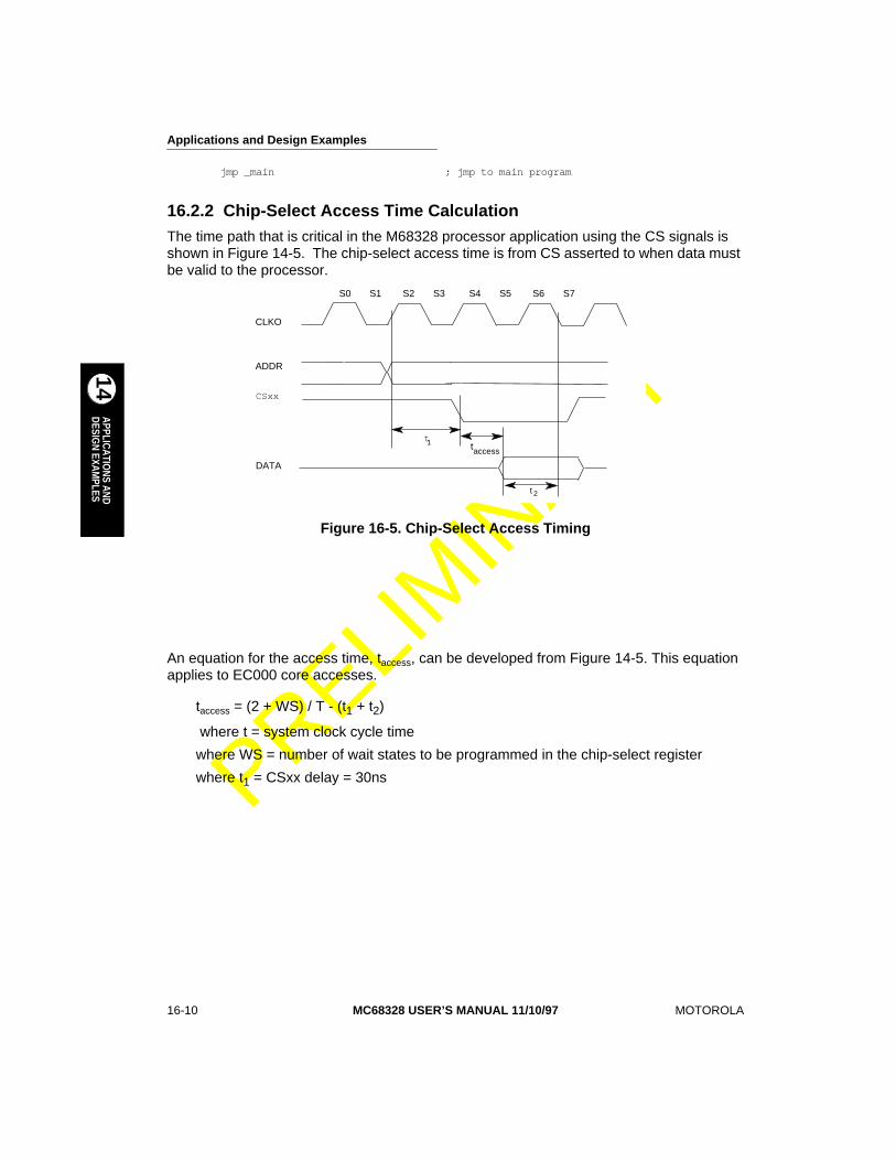
Applications and Design Examples
16-10
MC68328 USER’S MANUAL 11/10/97
MOTOROLA
APPLICATIONS AND
14
DESIGN EXAM
PLES
PRELIM
INARY
jmp _main ; jmp to main program
16.2.2 Chip-Select Access Time Calculation
The time path that is critical in the M68328 processor application using the CS signals is shown in Figure 14-5. The chip-select access time is from CS asserted to when data must be valid to the processor.
Figure 16-5. Chip-Select Access Timing
An equation for the access time, t
access
, can be developed from Figure 14-5. This equation applies to EC000 core accesses.
t
access
= (2 + WS) / T - (t
1
+ t
2
)
where t = system clock cycle time
where WS = number of wait states to be programmed in the chip-select register
where t
1
= CSxx delay = 30ns
CLKO
S0 S1 S2 S3 S4 S5 S6 S7
ADDR
CSxx
DATA
t1 taccess
t 2
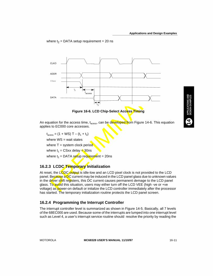
Applications and Design Examples
MOTOROLA
MC68328 USER’S MANUAL 11/10/97
16-11
APPL
ICAT
IONS
AND
14
DESI
GN
EXAM
PLES
PRELIM
INARY
where t
2
= DATA setup requirement = 20 ns
An equation for the access time, t
acess
, can be developed from Figure 14-6. This equation applies to EC000 core accesses.
t
acess
= (1 + WS) T – (t
1
+ t
2
)
where WS = wait states
where T = system clock period
where t
1
= CSxx delay = 30ns
where t
2
= DATA setup requirement = 20ns
16.2.3 LCDC Temporary Initialization
At reset, the LCDC output is idle-low and an LCD pixel clock is not provided to the LCD panel. Because a DC current may be induced in the LCD panel glass due to unknown values in the driver shift registers, this DC current causes permanent demage to the LCD panel glass. To avoid this situation, users may either turn off the LCD VEE (high -ve or +ve voltage) as power-on default or initalize the LCD controller immediately after the processor has started. The temporary initialization routine protects the LCD panel screen.
16.2.4 Programming the Interrupt Controller
The interrupt controller level is summarized as shown in Figure 14-5. Basically, all 7 levels of the 68EC000 are used. Because some of the interrupts are lumped into one interrupt level such as Level 4, a user’s interrupt service routine should resolve the priority by reading the
Figure 16-6. LCD Chip-Select Access Timing
CLKO
ADDR
CSxx
DATA
t1taccess
t 2
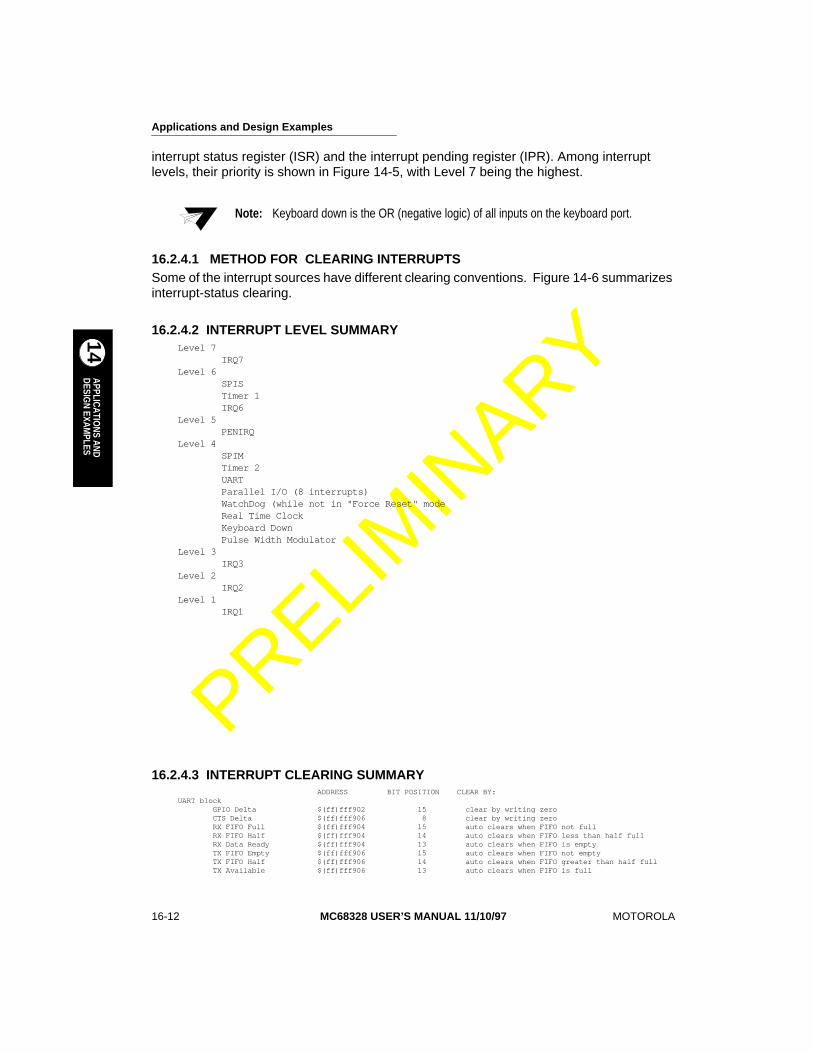
Applications and Design Examples
16-12
MC68328 USER’S MANUAL 11/10/97
MOTOROLA
APPLICATIONS AND
14DESIG
N EXAMPLES
PRELIM
INARY
interrupt status register (ISR) and the interrupt pending register (IPR). Among interrupt levels, their priority is shown in Figure 14-5, with Level 7 being the highest.
16.2.4.1 METHOD FOR CLEARING INTERRUPTSSome of the interrupt sources have different clearing conventions. Figure 14-6 summarizes interrupt-status clearing.
16.2.4.2 INTERRUPT LEVEL SUMMARYLevel 7 IRQ7Level 6 SPIS Timer 1 IRQ6Level 5 PENIRQLevel 4 SPIM Timer 2 UART Parallel I/O (8 interrupts) WatchDog (while not in "Force Reset" mode Real Time Clock Keyboard Down Pulse Width ModulatorLevel 3 IRQ3Level 2 IRQ2Level 1 IRQ1
16.2.4.3 INTERRUPT CLEARING SUMMARY ADDRESS BIT POSITION CLEAR BY:UART block GPIO Delta $(ff)fff902 15 clear by writing zero CTS Delta $(ff)fff906 8 clear by writing zero RX FIFO Full $(ff)fff904 15 auto clears when FIFO not full RX FIFO Half $(ff)fff904 14 auto clears when FIFO less than half full RX Data Ready $(ff)fff904 13 auto clears when FIFO is empty TX FIFO Empty $(ff)fff906 15 auto clears when FIFO not empty TX FIFO Half $(ff)fff906 14 auto clears when FIFO greater than half full TX Available $(ff)fff906 13 auto clears when FIFO is full
Note: Keyboard down is the OR (negative logic) of all inputs on the keyboard port.
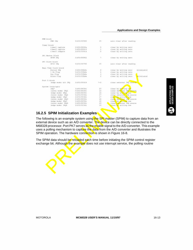
Applications and Design Examples
MOTOROLA MC68328 USER’S MANUAL 11/10/97 16-13
APPL
ICAT
IONS
AND
14DE
SIG
N EX
AMPL
ESPRELI
MIN
ARY
PWM block PWM IRQ $(ff)fff500 15 auto clear after reading Timer block timer1 capture $(ff)fff60a 0 clear by writing zero timer2 capture $(ff)fff616 1 clear by writing zero timer2 compare $(ff)fff616 0 clear by writing zero SPI Master block SPIM IRQ $(ff)fff802 7 clear by writing zero SPI Slave block SPIS IRQ $(ff)fff700 15 auto clear after reading Real Time Clock block Period IRQ $(ff)fffb0e 6 clear by writing zero (eliminate) 1 Hz Flag $(ff)fffb0e 4 clear by writing zero Day Flag $(ff)fffb0e 3 clear by writing zero Alarm Flag $(ff)fffb0e 2 clear by writing zero (eliminate) Port D block (edge mode) bit IRQ $(ff)fff418 7-0 clear external IRQ source System Interrupts IRQ7 $(ff)fff30c 23 clear by writing one (level mode) IRQ1 $(ff)fff30c 16 clear external IRQ source (edge mode) IRQ1 $(ff)fff30c 16 clear by writing one (level mode) IRQ2 $(ff)fff30c 17 clear external IRQ source (edge mode) IRQ2 $(ff)fff30c 17 clear by writing one (level mode) IRQ3 $(ff)fff30c 18 clear external IRQ source (edge mode) IRQ3 $(ff)fff30c 18 clear by writing one (level mode) IRQ6 $(ff)fff30c 19 clear external IRQ source (edge mode) IRQ6 $(ff)fff30c 19 clear by writing one
16.2.5 SPIM Initialization ExamplesThe following is an example system using the SPI master (SPIM) to capture data from an external device such as an A/D converter. The device can be directly connected to the M68328 processor. Port PK7 serves as the enable signal to the A/D converter. This example uses a polling mechanism to capture the data from the A/D converter and illustrates the SPIM operation. The hardware connection is shown in Figure 16-8.
The SPIM data should be reloaded each time before initiating the SPIM control register exchange bit. Although the example does not use interrupt service, the polling routine
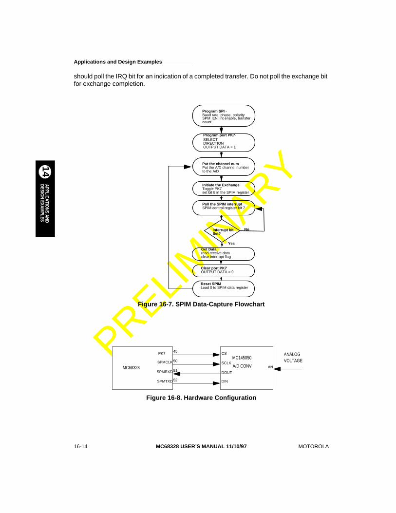
Applications and Design Examples
16-14 MC68328 USER’S MANUAL 11/10/97 MOTOROLA
APPLICATIONS AND
14DESIG
N EXAMPLES
PRELIM
INARY
should poll the IRQ bit for an indication of a completed transfer. Do not poll the exchange bit for exchange completion.
Figure 16-7. SPIM Data-Capture Flowchart
Figure 16-8. Hardware Configuration
Program SPI -
SPM_EN, int enable, transfer count
Program port PK7-SELECTDIRECTIONOUTPUT DATA = 1
Put the channel num
Baud rate, phase, polarity
Put the A/D channel number
Initiate the ExchangeToggle PK7
Poll the SPIM interruptSPIM control register bit 7
NoInterrupt bit
Get Dataread receive data clear interrupt flag
Yes
Clear port PK7OUTPUT DATA = 0
Reset SPIM Load 0 to SPIM data register
to the A/D
set bit 8 in the SPIM register
Set?
MC68328
MC145050
A/D CONV
52
51
50
45
SPMTXD
SPMRXD
SPMCLK
PK7
DIN
DOUT
SCLK
CS
AN
ANALOGVOLTAGE
Applications and Design Examples
MOTOROLA MC68328 USER’S MANUAL 11/10/97 16-15
APPL
ICAT
IONS
AND
14DE
SIG
N EX
AMPL
ESPRELI
MIN
ARY
16.3 POWER-SAVING TIPSYou can save power on the MC68328 by following these tips:
• Keep the core shut down as much as possible by putting it in doze mode. Set the STOP bit in the power control register during any peiod of inactivity.
• Shut down the PLL to enter sleep mode. Set the DISPLL bit in the PLL control register to conserve power when the processor is inactive for an extended period of time.
• Avoid the following pull-up resistor conditions to save the most power:
❏ When an internal pull-up is enabled on an input with an external device driving it low.
❏ When an internal pull-up is enabled on an I/O with the internal output device driving it low.
• Drive the outputs to their high state before entering sleep mode. The outputs have an internal pull-up that will not consume excess current when the pin is driven high. However, some external devices may require that the signal from the MC68328 port be low to save the most power.
• Disable the pull-ups on inputs that are always driven externally. Inputs that are continuously driven from an external device do not require an internal pull-up resistor. You can save power by disabling the internal pull-up resistor on the MC68328 I/O ports that are configured as inputs and always driven to a high or low state by the external device.
• Disable the I/O port internal pull-ups one by one to isolate excess current drain in sleep mode.
• Beware of outputs sourcing current for externally powered-down devices. When the MC68328 is powered down in sleep or doze mode, the output pins remain in the state they were in before going to sleep. This may cause an external device with its power turned off to try to power itself from the MC68328 output pins that are connected to it. In this case, it may be best to make sure the MC68328 output pin is in the low state and that internal pull-up is disabled.
• Open inputs will cause excess current drain. JTAG inputs are often forgotten.
• Inputs that are not being driven rail to rail consume excess current.
Applications and Design Examples
16-16 MC68328 USER’S MANUAL 11/10/97 MOTOROLA
APPLICATIONS AND
14DESIG
N EXAMPLES
PRELIM
INARY
16.3.1 LCD Refresh FrequencyThe following sequence of steps can be used to determine the values required for the PIXCLK divider (LCDC PXCD), last buffer address register (LBAR), and octet terminal count register (OTCR). These registers all affect the refresh rate of the LCD panel. The following example assumes a screes size of 240 × 160.
1. Calculate the pixel clock divider for grayscale.
DIV = (PIX_CLK_SOURCE) / (XMAX × 2 × YMAX × REFRESH_RATE) (for grayscale)
DIV = (PIX_CLK_SOURCE) / (XMAX × YMAX × REFRESH_RATE)
DIV = (16.58MHz) / (240 × 2 × 160 × 70) = 3.08 ≥3
Divider must be a whole number, so round to 3. Byte write $02 to PXCD register to set the divider equal to 3. Notice that PIX_CLK_SOURCE is derived from the PLL control register.
2. Last buffer address register (LBAR).
LBAR = 240 / 16 = 15
LBAR = 240 / 8 = 30 (for grayscale)
3. Calculate the value of the OTCR register. This value controls the time required between two line pulses. Select a value so that OTCR > LBAR, as required.
OTCR = LBAR + 4 = 19
OTCR = LBAR + 8 = 38 (for grayscale)
Increasing the value in OTCR will increase the LP period.
4. Calculate the frequency.
Frequency = 16.58MHz / (DIV × YMAX × OCTET × 16) = 16.58MHz / (3 × 160 × 38 × 16) (for grayscale) = 56MHz
If OCTET = 31, then frequency = 69Hz. OCTET is the OTCR register value.
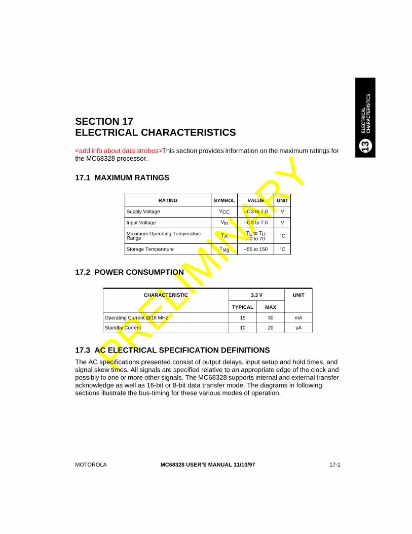
MOTOROLA
MC68328 USER’S MANUAL 11/10/97
17-1
ELEC
TRIC
AL
13
CHAR
ACTE
RIST
ICS
PRELIM
INARY
SECTION 17ELECTRICAL CHARACTERISTICS
<add info about data strobes>This section provides
information on the maximum ratings for the MC68328 processor.
17.1 MAXIMUM RATINGS
17.2 POWER CONSUMPTION
17.3 AC ELECTRICAL SPECIFICATION DEFINITIONS
The AC specifications presented consist of output delays, input setup and hold times, and signal skew times. All signals are specified relative to an appropriate edge of the clock and possibly to one or more other signals. The MC68328 supports internal and external transfer acknowledge as well as 16-bit or 8-bit data transfer mode. The diagrams in following sections illustrate the bus-timing for these various modes of operation.
RATING SYMBOL VALUE UNIT
Supply Voltage VCC –0.3 to 7.0 V
Input Voltage Vin –0.3 to 7.0 V
Maximum Operating Temperature Range TA
TL to TH–0 to 70
°
C
Storage Temperature Tstg –55 to 150
°
C
CHARACTERISTIC 3.3 V UNIT
TYPICAL MAX
Operating Current @16 MHz 15 30 mA
Standby Current 10 20 uA
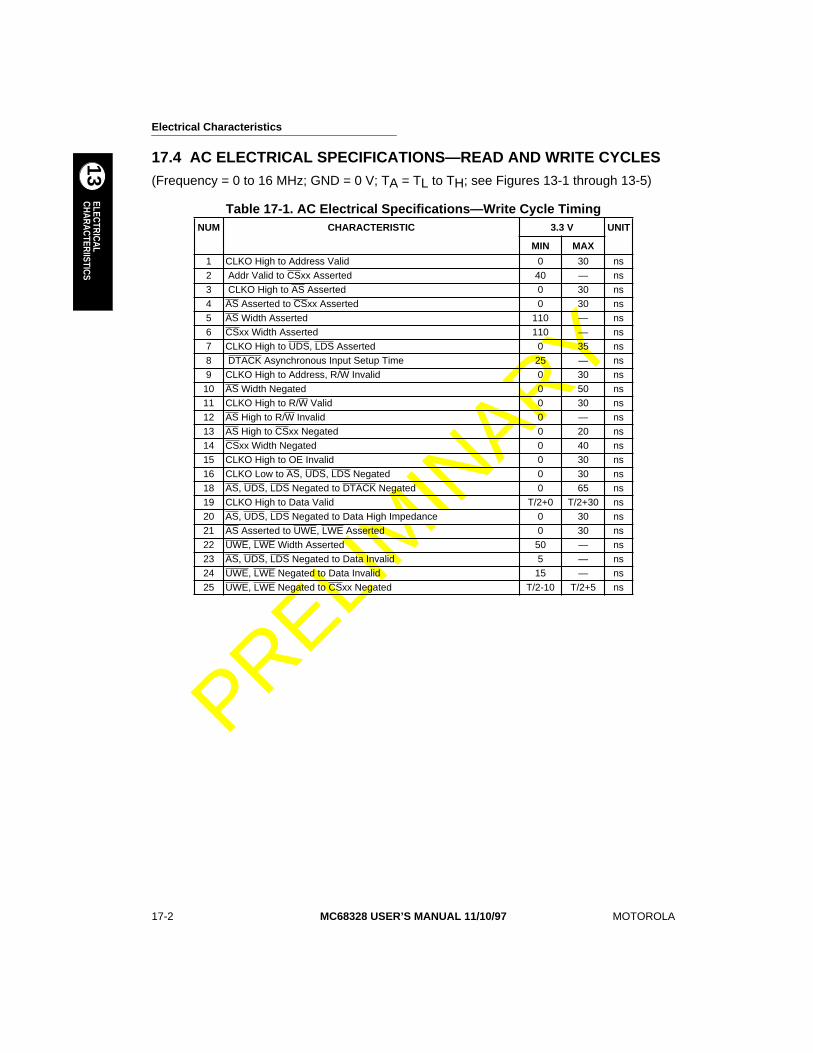
Electrical Characteristics
17-2
MC68328 USER’S MANUAL 11/10/97
MOTOROLA
ELECTRICAL
13
CHARACTERIISTICS
PRELIM
INARY
17.4 AC ELECTRICAL SPECIFICATIONS—READ AND WRITE CYCLES
(Frequency = 0 to 16 MHz; GND = 0 V; TA = TL to TH; see Figures 13-1 through 13-5)
Table 17-1. AC Electrical Specifications—Write Cycle Timing
NUM CHARACTERISTIC 3.3 V UNIT
MIN MAX
1 CLKO High to Address Valid 0 30 ns2 Addr Valid to CSxx Asserted 40 — ns3 CLKO High to AS Asserted 0 30 ns4 AS Asserted to CSxx Asserted 0 30 ns5 AS Width Asserted 110 — ns6 CSxx Width Asserted 110 — ns7 CLKO High to UDS, LDS Asserted 0 35 ns8 DTACK Asynchronous Input Setup Time 25 — ns9 CLKO High to Address, R/W Invalid 0 30 ns10 AS Width Negated 0 50 ns11 CLKO High to R/W Valid 0 30 ns12 AS High to R/W Invalid 0 — ns13 AS High to CSxx Negated 0 20 ns14 CSxx Width Negated 0 40 ns15 CLKO High to OE Invalid 0 30 ns16 CLKO Low to AS, UDS, LDS Negated 0 30 ns18 AS, UDS, LDS Negated to DTACK Negated 0 65 ns19 CLKO High to Data Valid T/2+0 T/2+30 ns20 AS, UDS, LDS Negated to Data High Impedance 0 30 ns21 AS Asserted to UWE, LWE Asserted 0 30 ns22 UWE, LWE Width Asserted 50 — ns23 AS, UDS, LDS Negated to Data Invalid 5 — ns24 UWE, LWE Negated to Data Invalid 15 — ns25 UWE, LWE Negated to CSxx Negated T/2-10 T/2+5 ns
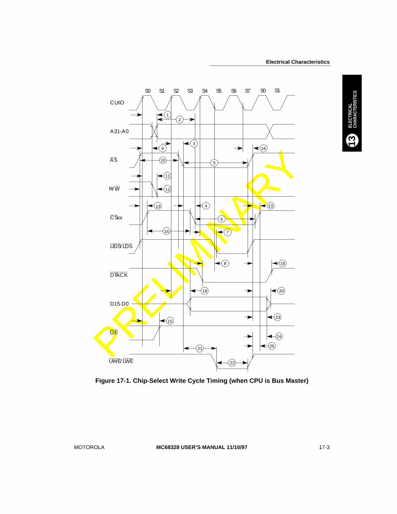
Electrical Characteristics
MOTOROLA
MC68328 USER’S MANUAL 11/10/97
17-3
ELEC
TRIC
AL
13
CHAR
ACTE
RIST
ICS
PRELIM
INARY
Figure 17-1. Chip-Select Write Cycle Timing (when CPU is Bus Master)
S0 S1 S2 S3 S4 S5 S6 S7 S0 S1
CLKO
A31-A0
AS
R/W
CSxx
UDS/LDS
DTACK
D15-D0
OE
510
1
3
4
169
13
11
12
6
13
14
18
15
19
8
20
23
7
UWE/LWE 22
2521
24
2
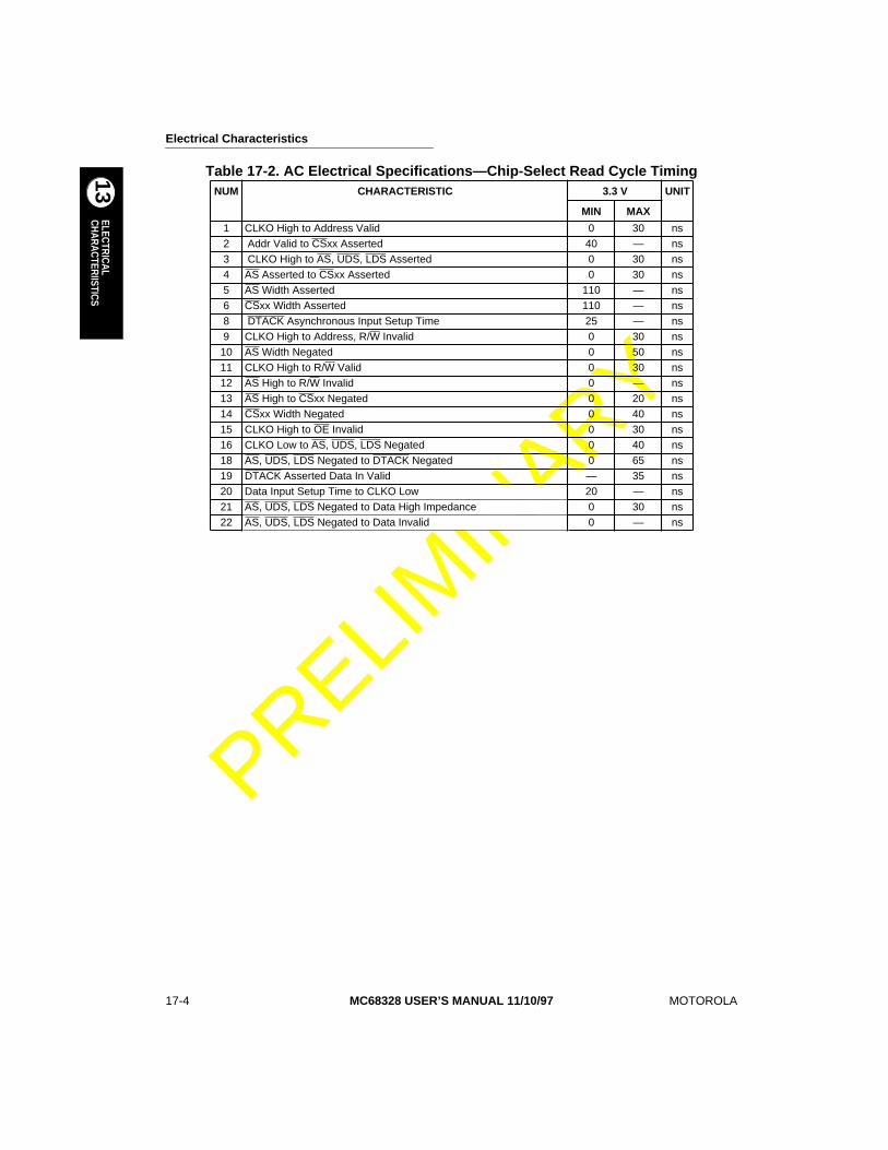
Electrical Characteristics
17-4
MC68328 USER’S MANUAL 11/10/97
MOTOROLA
ELECTRICAL
13
CHARACTERIISTICS
PRELIM
INARY
Table 17-2. AC Electrical Specifications—Chip-Select Read Cycle Timing
NUM CHARACTERISTIC 3.3 V UNIT
MIN MAX
1 CLKO High to Address Valid 0 30 ns2 Addr Valid to CSxx Asserted 40 — ns3 CLKO High to AS, UDS, LDS Asserted 0 30 ns4 AS Asserted to CSxx Asserted 0 30 ns5 AS Width Asserted 110 — ns6 CSxx Width Asserted 110 — ns8 DTACK Asynchronous Input Setup Time 25 — ns9 CLKO High to Address, R/W Invalid 0 30 ns10 AS Width Negated 0 50 ns11 CLKO High to R/W Valid 0 30 ns12 AS High to R/W Invalid 0 — ns13 AS High to CSxx Negated 0 20 ns14 CSxx Width Negated 0 40 ns15 CLKO High to OE Invalid 0 30 ns16 CLKO Low to AS, UDS, LDS Negated 0 40 ns18 AS, UDS, LDS Negated to DTACK Negated 0 65 ns19 DTACK Asserted Data In Valid — 35 ns20 Data Input Setup Time to CLKO Low 20 — ns21 AS, UDS, LDS Negated to Data High Impedance 0 30 ns22 AS, UDS, LDS Negated to Data Invalid 0 — ns
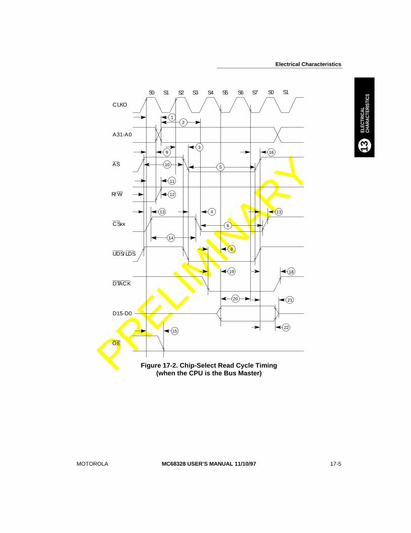
Electrical Characteristics
MOTOROLA
MC68328 USER’S MANUAL 11/10/97
17-5
ELEC
TRIC
AL
13
CHAR
ACTE
RIST
ICS
PRELIM
INARY
Figure 17-2. Chip-Select Read Cycle Timing(when the CPU is the Bus Master)
S0 S1 S2 S3 S4 S5 S6 S7 S0 S1
CLKO
A31-A0
AS
R/W
CSxx
UDS/LDS
DTACK
D15-D0
OE
510
1
3
4
169
13
11
12
6
13
14
18
15
20
19
21
22
8
2
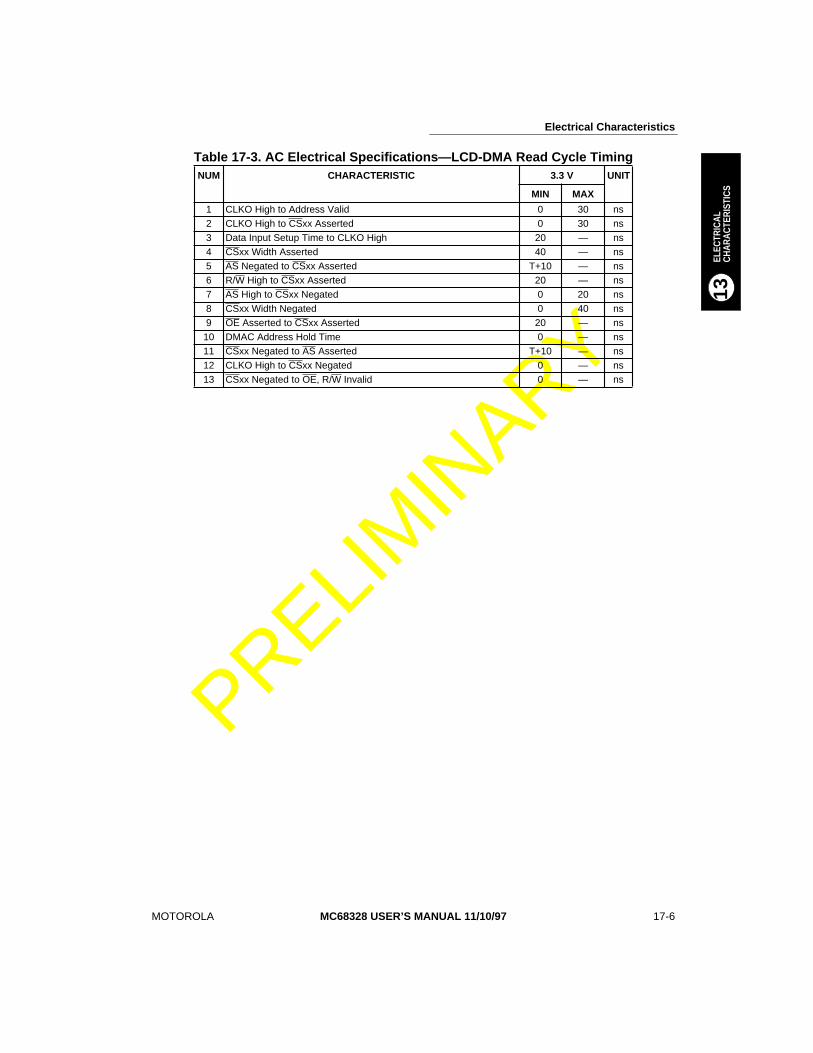
Electrical Characteristics
MOTOROLA
MC68328 USER’S MANUAL 11/10/97
17-6
ELEC
TRIC
AL
13
CHAR
ACTE
RIST
ICS
PRELIM
INARY
Table 17-3. AC Electrical Specifications—LCD-DMA Read Cycle Timing
NUM CHARACTERISTIC 3.3 V UNIT
MIN MAX
1 CLKO High to Address Valid 0 30 ns2 CLKO High to CSxx Asserted 0 30 ns3 Data Input Setup Time to CLKO High 20 — ns4 CSxx Width Asserted 40 — ns5 AS Negated to CSxx Asserted T+10 — ns6 R/W High to CSxx Asserted 20 — ns7 AS High to CSxx Negated 0 20 ns8 CSxx Width Negated 0 40 ns9 OE Asserted to CSxx Asserted 20 — ns
10 DMAC Address Hold Time 0 — ns11 CSxx Negated to AS Asserted T+10 — ns12 CLKO High to CSxx Negated 0 — ns13 CSxx Negated to OE, R/W Invalid 0 — ns
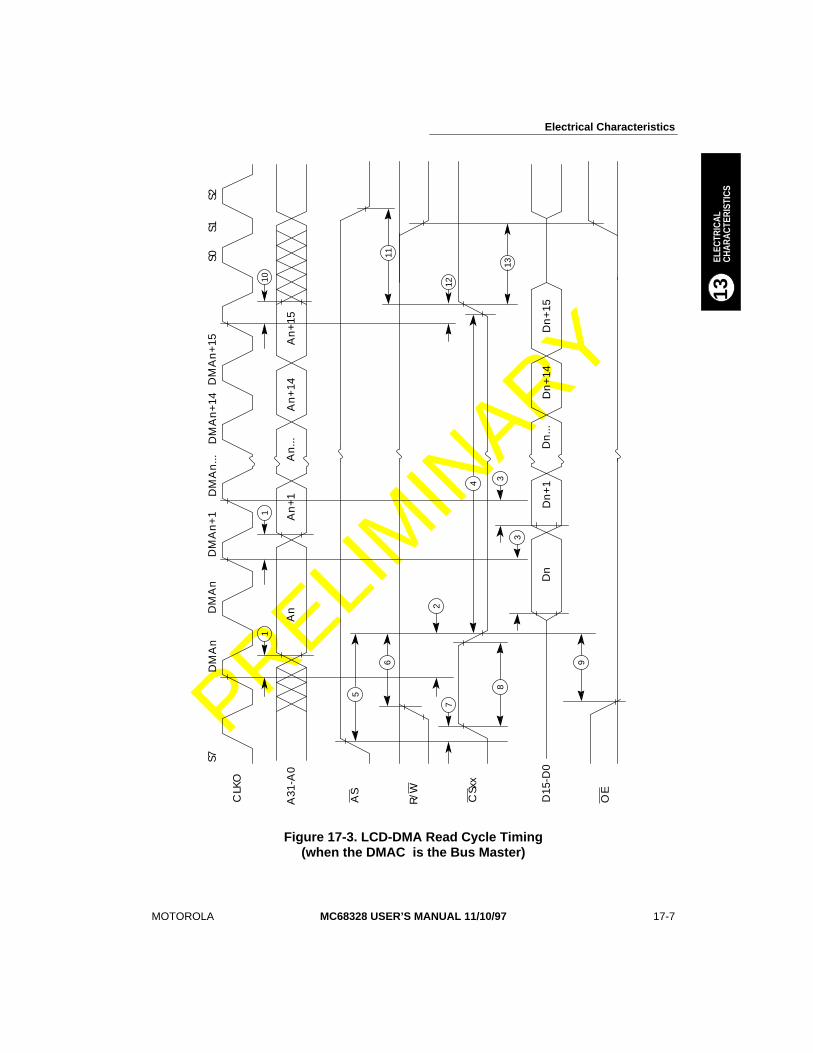
Electrical Characteristics
MOTOROLA
MC68328 USER’S MANUAL 11/10/97
17-7
ELEC
TRIC
AL
13
CHAR
ACTE
RIST
ICS
PRELIM
INARY
Figure 17-3. LCD-DMA Read Cycle Timing(when the DMAC is the Bus Master)
DM
An
CLK
O
A31
-A0
AS
R/W CSx
x
D15
-D0
OE
5
1
212
6
7
8
9
3
S0S1
S7D
MA
n+
1D
MA
n...
DM
An
+14
DM
An
+15
DM
An
13
An
An
+1
An
...A
n+
14A
n+
15
Dn
Dn
+1
Dn
...D
n+
14D
n+
15
1
34
11
10
S2
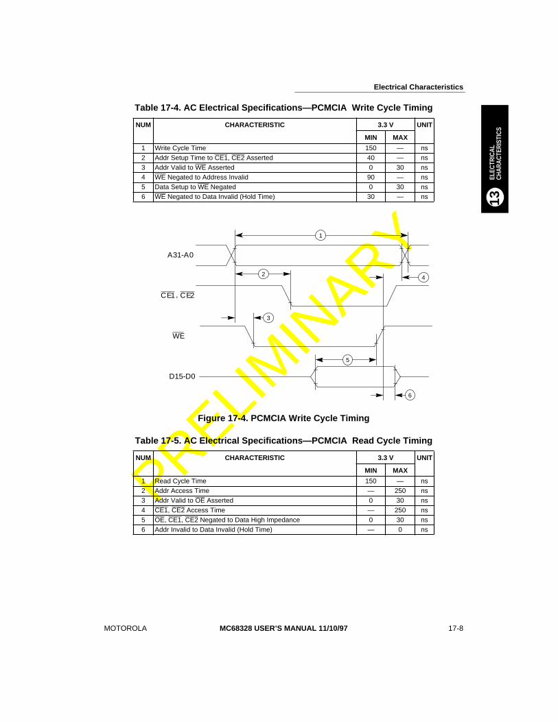
Electrical Characteristics
MOTOROLA
MC68328 USER’S MANUAL 11/10/97
17-8
ELEC
TRIC
AL
13
CHAR
ACTE
RIST
ICS
PRELIM
INARY
Table 17-4. AC Electrical Specifications—PCMCIA Write Cycle Timing
Figure 17-4. PCMCIA Write Cycle Timing
Table 17-5. AC Electrical Specifications—PCMCIA Read Cycle Timing
NUM CHARACTERISTIC 3.3 V UNIT
MIN MAX
1 Write Cycle Time 150 — ns2 Addr Setup Time to CE1, CE2 Asserted 40 — ns3 Addr Valid to WE Asserted 0 30 ns4 WE Negated to Address Invalid 90 — ns5 Data Setup to WE Negated 0 30 ns6 WE Negated to Data Invalid (Hold Time) 30 — ns
NUM CHARACTERISTIC 3.3 V UNIT
MIN MAX
1 Read Cycle Time 150 — ns2 Addr Access Time — 250 ns3 Addr Valid to OE Asserted 0 30 ns4 CE1, CE2 Access Time — 250 ns5 OE, CE1, CE2 Negated to Data High Impedance 0 30 ns6 Addr Invalid to Data Invalid (Hold Time) — 0 ns
A31-A0
CE1
D15-D0
WE
1
2
6
CE2,
3
4
5
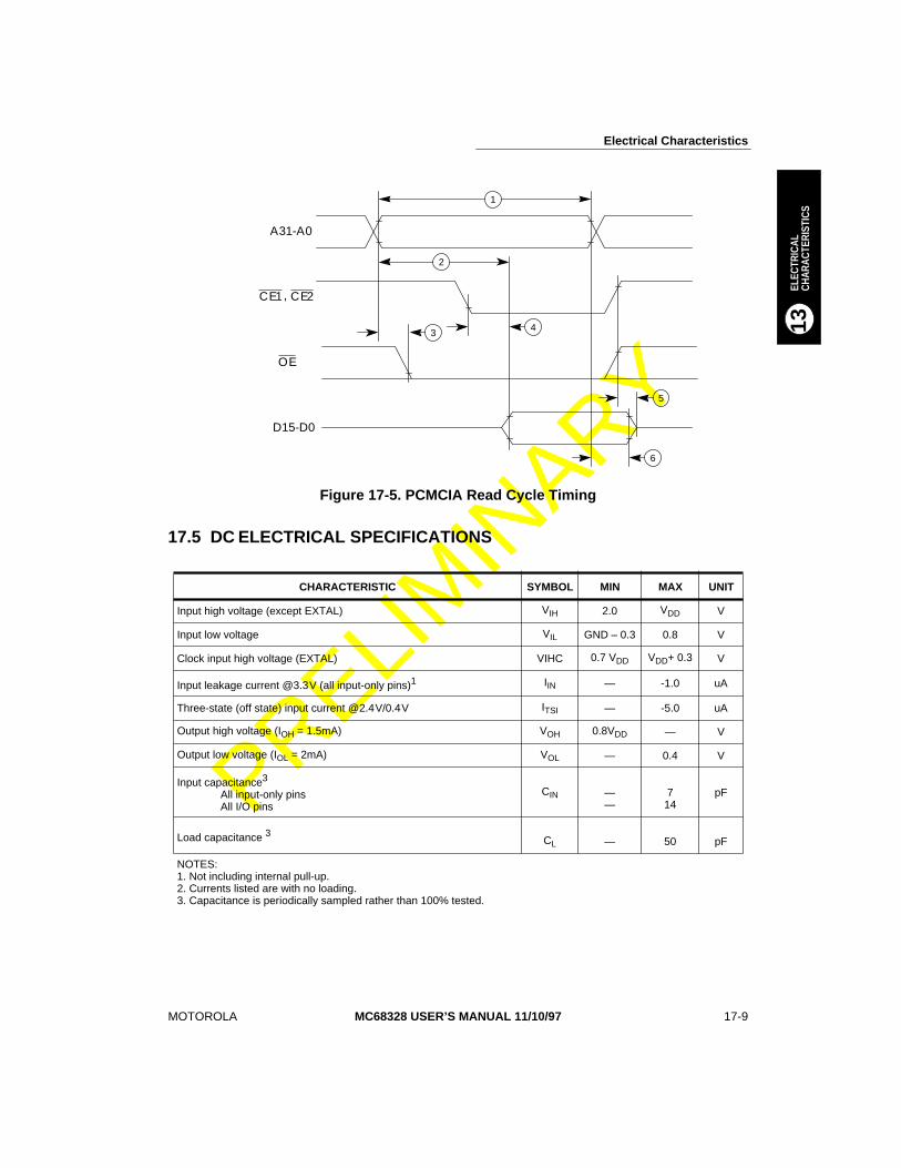
Electrical Characteristics
MOTOROLA
MC68328 USER’S MANUAL 11/10/97
17-9
ELEC
TRIC
AL
13
CHAR
ACTE
RIST
ICS
PRELIM
INARY
Figure 17-5. PCMCIA Read Cycle Timing
17.5 DC
ELECTRICAL SPECIFICATIONS
CHARACTERISTIC SYMBOL MIN MAX UNIT
Input high voltage (except EXTAL) V
IH
2.0 V
DD
V
Input low voltage V
IL
GND – 0.3 0.8 V
Clock input high voltage (EXTAL) VIHC 0.7 V
DD
V
DD
+ 0.3 V
Input leakage current @3.3V (all input-only pins)
1
I
IN
— -1.0 uA
Three-state (off state) input current @2.4V/0.4V I
TSI
— -5.0 uA
Output high voltage (I
OH
= 1.5mA) V
OH
0.8V
DD
— V
Output low voltage (I
OL
= 2mA) V
OL
— 0.4 V
Input capacitance
3
All input-only pinsAll I/O pins
C
IN
——
714
pF
Load capacitance
3
C
L
— 50 pF
NOTES:1. Not including internal pull-up.2. Currents listed are with no loading.3. Capacitance is periodically sampled rather than 100% tested.
A31-A0
CE1
D15-D0
OE
1
2
5
6
CE2,
43

Electrical Characteristics
MOTOROLA
MC68328 USER’S MANUAL 11/10/97
17-10
ELEC
TRIC
AL
13
CHAR
ACTE
RIST
ICS
PRELIM
INARY
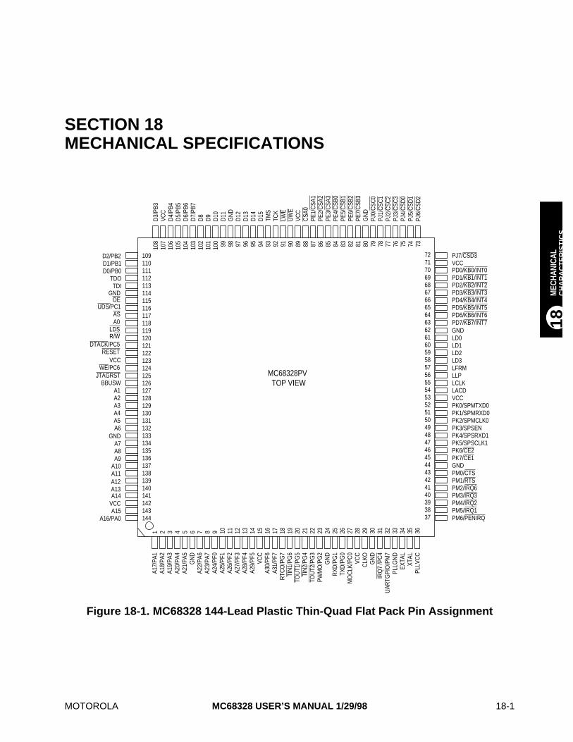
MOTOROLA
MC68328 USER’S MANUAL 1/29/98
18-1
MEC
HANI
CAL
18
CHAR
ACTE
RIST
ICS
SECTION 18MECHANICAL SPECIFICATIONS
Figure 18-1. MC68328 144-Lead Plastic Thin-Quad Flat Pack Pin Assignment
1 2 3 4 5 6 7 8 9 10 11 12 13 14 15 16 17 18 19 20 21 22 23 24 25 26 27 28 29 30 31 32 33 34 35 36
PM6/PENIRQPM5/IRQ1PM4/IRQ2PM3/IRQ3PM2/IRQ6PM1/RTSPM0/CTSGNDPK7/CE1PK6/CE2PK5/SPSCLK1PK4/SPSRXD1PK3/SPSENPK2/SPMCLK0PK1/SPMRXD0PK0/SPMTXD0VCCLACDLCLKLLPLFRMLD3LD2LD1LD0GND
PD0/KB0/INT0
PD7/KB7/INT7PD6/KB6/INT6PD5/KB5/INT5PD4/KB4/INT4PD3/KB3/INT3PD2/KB2/INT2PD1/KB1/INT1
VCCPJ7/CSD3
108
107
106
105
104
103
102
101
100 99 98 97 96 95 94 93 92 91 90 89 88 87 86 85 84 83 82 81 80 79 78 77 76 75 74 73
D3/
PB3
VCC
D4/
PB4
D5/
PB5
D6/
PB6
D7/
PB7
D8
D9
D10
D11
GN
DD
12D
13D
14D
15TM
STC
KLW
EU
WE
VCC
CSA
0PE
1/C
SA1
PE2/
CSA
2PE
3/C
SA3
PE4/
CSB
0PE
5/C
SB1
PE6/
CSB
2PE
7/C
SB3
GN
DPJ
0/C
SC0
PJ1/
CSC
1PJ
2/C
SC2
PJ3/
CSC
3PJ
4/C
SD0
PJ5/
CSD
1PJ
6/C
SD2
144143142141140139138137136135134133132131130129128127126125124123122121120119118117116115114113112111110109
373839404142434445464748495051525354555657585960616263646566676869707172
MC68328PVTOP VIEW
A13A14
A15A16/PA0
A17/
PA1
A18/
PA2
A19/
PA3
A20/
PA4
A21/
PA5
A22/
PA6
A23/
PA7
A24/
PF0
A25/
PF1
A26/
PF2
A27/
PF3
A28/
PF4
A29/
PF5
A30/
PF6
A31/
PF7
RTC
O/P
G7
TIN
1 /PG
6TO
UT1
/PG
5TI
N2 /
PG4
TOU
T2/P
G3
PWM
O/P
G2
RXD
/PG
1TX
D/P
G0
A12
GN
D
VCC
GN
D
UAR
TGPI
O/P
M7
A11A10
A9A8A7
A6A5A4A3A2A1
JTAGRSTBBUSW
MO
CLK
/PC
0
CLK
O
PLLG
ND
XTAL
PLLV
CC
EXTA
L
GND
VCC
RESETDTACK/PC5
A0LDSR/W
OE
WE/PC6
AS
TDOD0/PB0D1/PB1D2/PB2
TDI
VCC
GND
UDS/PC1
VCC
GN
DIR
Q7
/PC
4
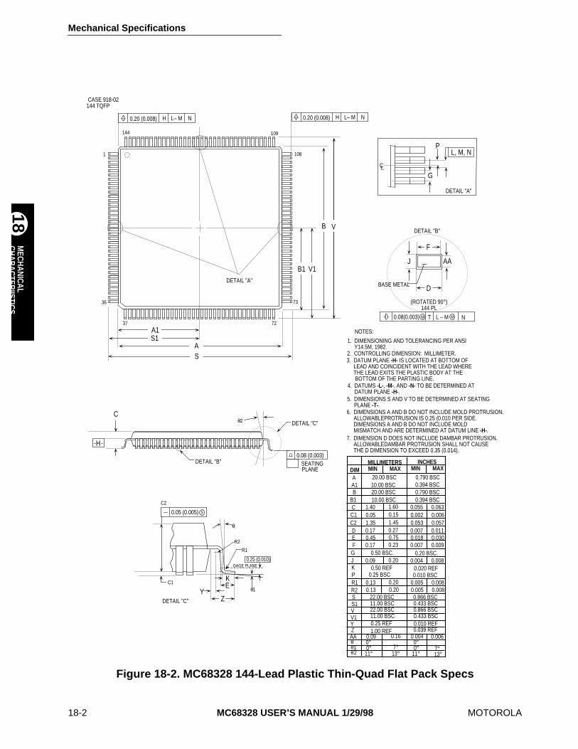
Mechanical Specifications
18-2
MC68328 USER’S MANUAL 1/29/98
MOTOROLA
MECHANICAL
18
CHARACTERIISTICS
Figure 18-2. MC68328 144-Lead Plastic Thin-Quad Flat Pack Specs
0.20 (0.008) L– M NH 0.20 (0.008) L– M NH
CL
DETAIL "C"
KE
Y
DIMA
MILLIMETERSMIN MAX
INCHESMIN MAX
20.00 BSC
20.00 BSC
NOTES:
1. DIMENSIONING AND TOLERANCING PER ANSI Y14.5M, 1982. 2. CONTROLLING DIMENSION: MILLIMETER.
3. DATUM PLANE -H- IS LOCATED AT BOTTOM OF LEAD AND COINCIDENT WITH THE LEAD WHERE THE LEAD EXITS THE PLASTIC BODY AT THE BOTTOM OF THE PARTING LINE.
4. DATUMS -L-, -M-, AND -N- TO BE DETERMINED AT DATUM PLANE -H-.
5. DIMENSIONS S AND V TO BE DETERMINED AT SEATING PLANE -T-.6. DIMENSIONS A AND B DO NOT INCLUDE MOLD PROTRUSION. ALLOWABLEPROTRUSION IS 0.25 (0.010 PER SIDE. DIMENSIONS A AND B DO NOT INCLUDE MOLD MISMATCH AND ARE DETERMINED AT DATUM LINE -H-.7. DIMENSION D DOES NOT INCLUDE DAMBAR PROTRUSION. ALLOWABLEDAMBAR PROTRUSION SHALL NOT CAUSE THE D DIMENSION TO EXCEED 0.35 (0.014).
H∩ 0.08 (0.003)
SEATINGPLANE
DETAIL "C"
DETAIL "B"
DETAIL "B"
BASE METAL
0.08(0.003) T L – M NM M
S
DETAIL "A"
DETAIL "A"
(ROTATED 90°)144 PL
G
P
CASE 918-02144 TQFP
BB1
0.790 BSC
22.00 BSC 0.866 BSC11.00 BSC 0.433 BSC22.00 BSC 0.866 BSC11.00 BSC 0.433 BSC
0.790 BSC10.00 BSC
10.00 BSC
0.25 BSC 0.010 BSC
0.394 BSC
0.394 BSC
C
DEF
JG
SS1VV1Y
KPR1R2
AA
0.50 BSC. 0.20 BSC.
Z
A1
C1C2
0.002 0.0060.150.050.053 0.0571.451.350.007 0.0110.270.170.018 0.0300.750.450.007 0.0090.230.17
0.004 0.0080.200.09
0.005 0.0080.200.130.005 0.0080.200.13
0.160.09 0.0060.0040°0°
0° 7° 0° 7°13°11° 13°11°
12
0.50 REF 0.020 REF
0.25 REF 0.010 REF1.00 REF 0.039 REF
0.055 0.0631.601.40
R1
GAGE PLANE
1
2
R2
C1
C2
0.25 (0.010)
C
T
AS1A1
S
B
V1B1
72
73
108
109144
1
37
36
D
F
J AA
L, M, N
0.05 (0.005)
θ
θ
θ
θθθ
Z
V
Mechanical Specifications
MOTOROLA
MC68328 USER’S MANUAL 1/29/98
18-3
MEC
HANI
CAL
18
CHAR
ACTE
RIST
ICS
Mechanical Specifications
18-4
MC68328 USER’S MANUAL 1/29/98
MOTOROLA
MECHANICAL
18
CHARACTERIISTICS
Related Documents