SCANSTA112 www.ti.com SNLS161I – DECEMBER 2002 – REVISED APRIL 2013 SCANSTA112 7-Port Multidrop IEEE 1149.1 (JTAG) Multiplexer Check for Samples: SCANSTA112 1FEATURES DESCRIPTION The SCANSTA112 extends the IEEE Std. 1149.1 test 2• True IEEE 1149.1 Hierarchical and Multidrop bus into a multidrop test bus environment. The Addressable Capability advantage of a multidrop approach over a single • The 8 Address Inputs Support up to 249 serial scan chain is improved test throughput and the Unique Slot Addresses, an Interrogation ability to remove a board from the system and retain Address, Broadcast Address, and 4 Multi-Cast test access to the remaining modules. Each Group Addresses (Address 000000 is SCANSTA112 supports up to 7 local IEEE1149.1 scan chains which can be accessed individually or Reserved) combined serially. • 7 IEEE 1149.1-Compatible Configurable Local Scan Ports Addressing is accomplished by loading the instruction register with a value matching that of the Slot inputs. • Bi-directional Backplane and LSP 0 Ports are Backplane and inter-board testing can easily be Interchangeable Slave Ports accomplished by parking the local TAP Controllers in • Capable of Ignoring TRST of the Backplane one of the stable TAP Controller states via a Park Port when it Becomes the Slave. instruction. The 32-bit TCK counter enables built in • Stitcher Mode Bypasses Level 1 and 2 self test operations to be performed on one port while other scan chains are simultaneously tested. Protocols • Mode Register 0 Allows Local TAPs to be The STA112 has a unique feature in that the Bypassed, Selected for Insertion into the Scan backplane port and the LSP0 port are bidirectional. They can be configured to alternatively act as the Chain Individually, or Serially in Groups of master or slave port so an alternate test master can Two or Three take control of the entire scan chain network from the • Transparent Mode can be Enabled with a LSP0 port while the backplane port becomes a slave. Single Instruction to Conveniently Buffer the Backplane IEEE 1149.1 Pins to Those on a Single Local Scan Port • General Purpose Local Port Pass Through Bits are Useful for Delivering Write Pulses for Flash Programming or Monitoring Device Status. • Known Power-Up State • TRST on all Local Scan Ports • 32-bit TCK Counter • 16-bit LFSR Signature Compactor • Local TAPs can Become TRI-STATE via the OE Input to Allow an Alternate Test Master to Take Control of the Local TAPs (LSP 0-3 have a TRI- STATE Notification Output) • 3.0-3.6V V CC Supply Operation • Supports Live Insertion/Withdrawal 1 Please be aware that an important notice concerning availability, standard warranty, and use in critical applications of Texas Instruments semiconductor products and disclaimers thereto appears at the end of this data sheet. 2All trademarks are the property of their respective owners. PRODUCTION DATA information is current as of publication date. Copyright © 2002–2013, Texas Instruments Incorporated Products conform to specifications per the terms of the Texas Instruments standard warranty. Production processing does not necessarily include testing of all parameters.

Welcome message from author
This document is posted to help you gain knowledge. Please leave a comment to let me know what you think about it! Share it to your friends and learn new things together.
Transcript
SCANSTA112
www.ti.com SNLS161I –DECEMBER 2002–REVISED APRIL 2013
SCANSTA112 7-Port Multidrop IEEE 1149.1 (JTAG) MultiplexerCheck for Samples: SCANSTA112
1FEATURES DESCRIPTIONThe SCANSTA112 extends the IEEE Std. 1149.1 test
2• True IEEE 1149.1 Hierarchical and Multidropbus into a multidrop test bus environment. TheAddressable Capabilityadvantage of a multidrop approach over a single
• The 8 Address Inputs Support up to 249 serial scan chain is improved test throughput and theUnique Slot Addresses, an Interrogation ability to remove a board from the system and retainAddress, Broadcast Address, and 4 Multi-Cast test access to the remaining modules. EachGroup Addresses (Address 000000 is SCANSTA112 supports up to 7 local IEEE1149.1
scan chains which can be accessed individually orReserved)combined serially.• 7 IEEE 1149.1-Compatible Configurable Local
Scan Ports Addressing is accomplished by loading the instructionregister with a value matching that of the Slot inputs.• Bi-directional Backplane and LSP0 Ports areBackplane and inter-board testing can easily beInterchangeable Slave Portsaccomplished by parking the local TAP Controllers in
• Capable of Ignoring TRST of the Backplane one of the stable TAP Controller states via a ParkPort when it Becomes the Slave. instruction. The 32-bit TCK counter enables built in
• Stitcher Mode Bypasses Level 1 and 2 self test operations to be performed on one port whileother scan chains are simultaneously tested.Protocols
• Mode Register0 Allows Local TAPs to be The STA112 has a unique feature in that theBypassed, Selected for Insertion into the Scan backplane port and the LSP0 port are bidirectional.
They can be configured to alternatively act as theChain Individually, or Serially in Groups ofmaster or slave port so an alternate test master canTwo or Threetake control of the entire scan chain network from the• Transparent Mode can be Enabled with aLSP0 port while the backplane port becomes a slave.Single Instruction to Conveniently Buffer the
Backplane IEEE 1149.1 Pins to Those on aSingle Local Scan Port
• General Purpose Local Port Pass Through Bitsare Useful for Delivering Write Pulses for FlashProgramming or Monitoring Device Status.
• Known Power-Up State• TRST on all Local Scan Ports• 32-bit TCK Counter• 16-bit LFSR Signature Compactor• Local TAPs can Become TRI-STATE via the OE
Input to Allow an Alternate Test Master to TakeControl of the Local TAPs (LSP0-3 have a TRI-STATE Notification Output)
• 3.0-3.6V VCC Supply Operation• Supports Live Insertion/Withdrawal
1
Please be aware that an important notice concerning availability, standard warranty, and use in critical applications ofTexas Instruments semiconductor products and disclaimers thereto appears at the end of this data sheet.
2All trademarks are the property of their respective owners.
PRODUCTION DATA information is current as of publication date. Copyright © 2002–2013, Texas Instruments IncorporatedProducts conform to specifications per the terms of the TexasInstruments standard warranty. Production processing does notnecessarily include testing of all parameters.
ST
A1
12
ST
A1
12
ST
A1
12
ST
A1
12
ST
A1
12
ST
A1
12
Backplane IEEE
1149.1
Test Bus
ASIC
with
JTAG
Backplane
IEEE 1149.1
Test Bus
Buffer with
JTAG
Buffer with
JTAG
Buffer with
JTAG
Flash
Memory
R/W
SCANSTA112
FPGA
vendor1
with JTAG
FPGA
vendor2
with JTAG
Processor
with JTAG
LSP0 LSP1 LSP2
LSP3
LSP4
SCANSTA112
SNLS161I –DECEMBER 2002–REVISED APRIL 2013 www.ti.com
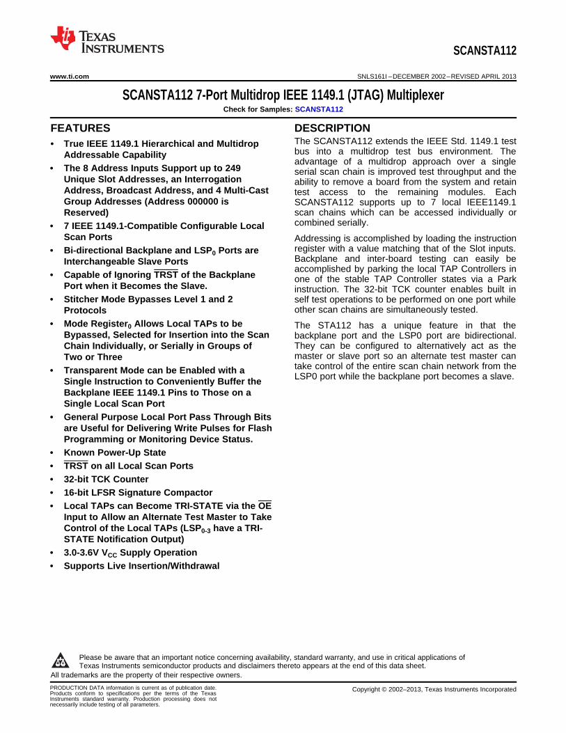
Figure 1. Typical use of SCANSTA112 for board-level management of multiple scan chains.
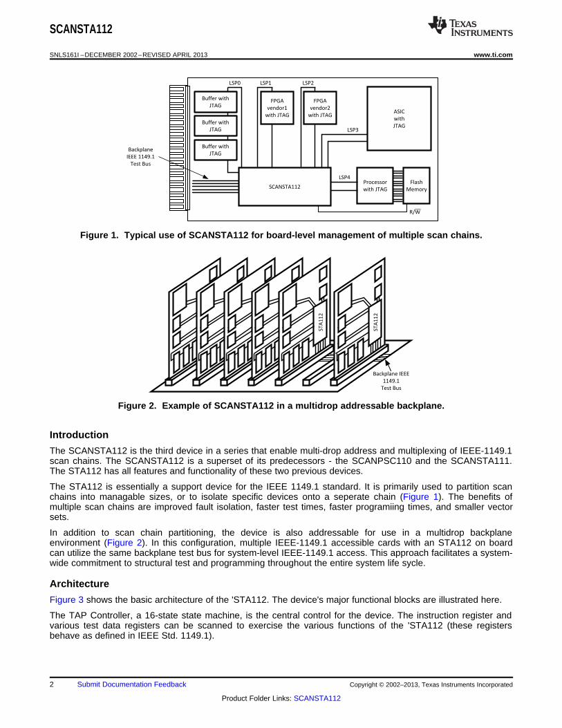
Figure 2. Example of SCANSTA112 in a multidrop addressable backplane.
Introduction
The SCANSTA112 is the third device in a series that enable multi-drop address and multiplexing of IEEE-1149.1scan chains. The SCANSTA112 is a superset of its predecessors - the SCANPSC110 and the SCANSTA111.The STA112 has all features and functionality of these two previous devices.
The STA112 is essentially a support device for the IEEE 1149.1 standard. It is primarily used to partition scanchains into managable sizes, or to isolate specific devices onto a seperate chain (Figure 1). The benefits ofmultiple scan chains are improved fault isolation, faster test times, faster programiing times, and smaller vectorsets.
In addition to scan chain partitioning, the device is also addressable for use in a multidrop backplaneenvironment (Figure 2). In this configuration, multiple IEEE-1149.1 accessible cards with an STA112 on boardcan utilize the same backplane test bus for system-level IEEE-1149.1 access. This approach facilitates a system-wide commitment to structural test and programming throughout the entire system life sycle.
Architecture
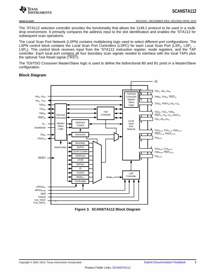
Figure 3 shows the basic architecture of the 'STA112. The device's major functional blocks are illustrated here.
The TAP Controller, a 16-state state machine, is the central control for the device. The instruction register andvarious test data registers can be scanned to exercise the various functions of the 'STA112 (these registersbehave as defined in IEEE Std. 1149.1).
2 Submit Documentation Feedback Copyright © 2002–2013, Texas Instruments Incorporated
Product Folder Links: SCANSTA112
Boundary
32-bit Counter
SGPIO
Mode0-3
Control
ID
ByPass
LFSR
MultiCast
PortEnable
Instruction
SelectionControl
TAPController
LocalScanPort
Network
LSPController
TCKB0
TMSB0
TRSTB0
S0-7
TDIB0
A0B0, A1B0
Y0B0, Y1B0
TDOB0
Mode0-3
TDI/TDOCrossover
Master/SlaveLogic
TDIB1, A0B1 A1B1
TMSB1 TCKB1 TRSTB1
TDOB1 TRISTB1Y0B1 Y1B1
TRISTB0
TDO01 TCK01 TMS01 TRST01 Y001 Y101 TRIST01
TDI01 A001 A101
LSPSel0-6
MPSelB1/B0
TRANS
TDO02-03 TCK02_03 TMS02-03 TRST02-03 TRIST02-03
TDI02-03
TDO04-06 TCK04-06 TMS04-06 TRST04-06
TDI04-06
OE
MstrPortSel
ADDMASK
SB/S
RESET
TLR_TRSTTLR_TRST6
TDI/TDOCrossover
Master/SlaveLogic
/2
SCANSTA112
www.ti.com SNLS161I –DECEMBER 2002–REVISED APRIL 2013
The 'STA112 selection controller provides the functionality that allows the 1149.1 protocol to be used in a multi-drop environment. It primarily compares the address input to the slot identification and enables the 'STA112 forsubsequent scan operations.
The Local Scan Port Network (LSPN) contains multiplexing logic used to select different port configurations. TheLSPN control block contains the Local Scan Port Controllers (LSPC) for each Local Scan Port (LSP0, LSP1 ...LSPn). This control block receives input from the 'STA112 instruction register, mode registers, and the TAPcontroller. Each local port contains all four boundary scan signals needed to interface with the local TAPs plusthe optional Test Reset signal (TRST).
The TDI/TDO Crossover Master/Slave logic is used to define the bidirectional B0 and B1 ports in a Master/Slaveconfiguration.
Block Diagram
Figure 3. SCANSTA112 Block Diagram
Copyright © 2002–2013, Texas Instruments Incorporated Submit Documentation Feedback 3
Product Folder Links: SCANSTA112
A3 A4 A5 A6A2A1
B7B3 B4 B5 B6B2B1
C7C3 C4 C5 C6C2C1
D7D3 D4 D5 D6D2D1
E7E3 E4 E5 E6E2E1
F7F3 F4 F5 F6F2F1
G7G3 G4 G5 G6G2G1
A7
B8
C8
D8
E8
F8
G8
A8
B9
C9
D9
E9
F9
G9
A9
B10
C10
D10
E10
F10
G10
A10
H7H3 H4 H5 H6H2H1 H8 H9 H10
J7J3 J4 J5 J6J2J1 J8 J9 J10
K7K3 K4 K5 K6K2K1 K8 K9 K10
VCC
VCC
VCC
VCC
VCC
VCC
VCC
VCC
VCC
S0
TMSB0
GND
S7
ADDMASK
OE
GND
LSPsel5
TCK06
TCK05
TCK04
TCK03
TCK01
TCK02
S1
S3
TRANS
LSPsel0
LSPsel2
LSPsel4
LSPsel3
LSPsel6
LSPsel1
MPselB1/B0
TDIB0
TDOB0
TDO06
GND
S5
S6
GND
TCKB0
TRISTB0
TDI06
TMS06
S4
S2
SB/S
TRSTB0
Y1B0
Y0B0
TMS05
TRST05
TRST06
A0B1
A0B0
A1B0
TDOB1
GND
GND
GND
VCC
GND
GND GND
TDO05
TDO04
TRST03
TDI05
A001
A1B1
TRSTB1
TCKB1
TDIB1
TRST04
TDI04
TRIST03
TDI03
RESET
TDO01
TRISTB1
TMSB1
TMS04
TRST02
TDO02
TMS01
Y1B1
TMS03
TMS02
TDI02
Y001
Y101
TDI01
TLRTRST6
Y0B1 TLRTRST
TRST01
TRIST01
A101
TRIST02
TDO03
SCANSTA112
SNLS161I –DECEMBER 2002–REVISED APRIL 2013 www.ti.com
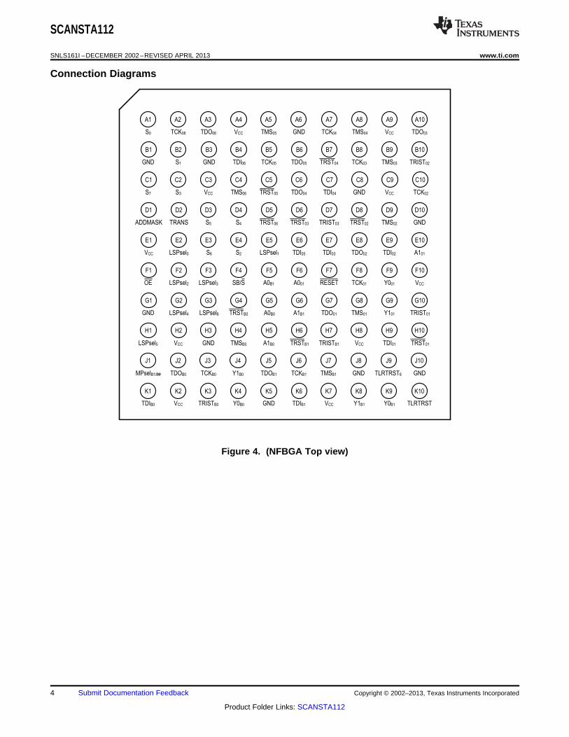
Connection Diagrams
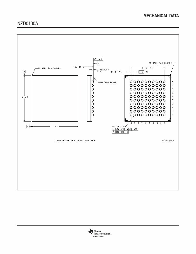
Figure 4. (NFBGA Top view)
4 Submit Documentation Feedback Copyright © 2002–2013, Texas Instruments Incorporated
Product Folder Links: SCANSTA112
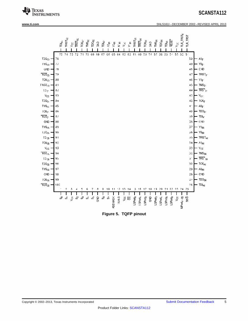
SCANSTA112
www.ti.com SNLS161I –DECEMBER 2002–REVISED APRIL 2013
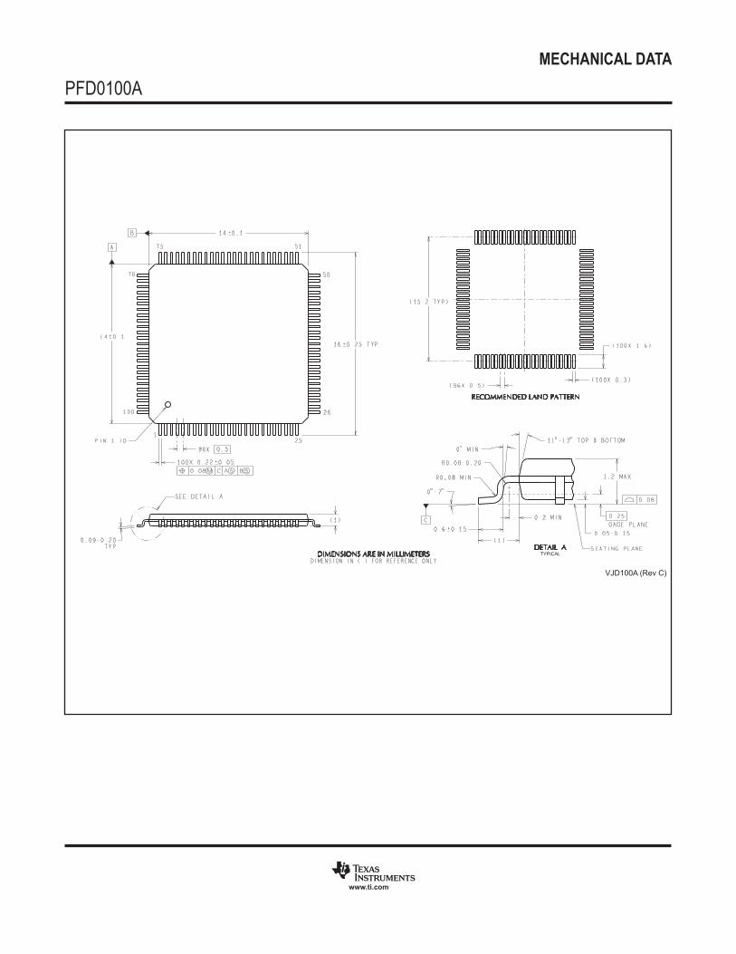
Figure 5. TQFP pinout
Copyright © 2002–2013, Texas Instruments Incorporated Submit Documentation Feedback 5
Product Folder Links: SCANSTA112
SCANSTA112
SNLS161I –DECEMBER 2002–REVISED APRIL 2013 www.ti.com
PIN DESCRIPTIONSNo.
Pin Name Pins I/O Description
VCC 10 N/A Power
GND 10 N/A Ground
RESET 1 I RESET Input: will force a reset of the device regardless of the current state.
ADDMASK 1 I ADDRESS MASK input: Allows masking of lower slot input pins.
MPselB1/B0 1 I MASTER PORT SELECTION: Controls selection of LSPB0 or LSPB1 as the backplane port. Theunselected port becomes LSP00. A value of "0" will select LSPB0 as the master port.
SB/S 1 I Selects ScanBridge or Stitcher Mode.
LSPsel (0-6) 7 I In Stitcher Mode these inputs define which LSP's are to be included in the scan chain
TRANS 1 I Transparent Mode enable input: The value of this pin is loaded into the TRANSENABLE bit of thecontrol register at power-up. This value is used to control the presence of registers and pad-bits inthe scan chain while in the stitcher mode.
TLR_TRST 1 I Sets the driven value of TRST0-5 when LSP TAPs are in TLR and the device is not being reset.During RESET = "0" or TRSTB = "0" (IgnoreReset = "0") TRSTn = "0". This pin is to be tied low tomatch the function of the SCANSTA111
TLR_TRST6 1 I This pin affects TRST of LSP6 only. This pin is to be tied low to match the function of theSCANSTA111
TDIB0, TDIB1 2 I BACKPLANE TEST DATA INPUT: All backplane scan data is supplied to the 'STA112 through thisinput pin. MPselB1/B0 determines which port is the master backplane port and which is LSP00. Thisinput has a 25KΩ internal pull-up resistor and no ESD clamp diode (ESD is controlled with analternate method). When the device is power-off (VDD floating), this input appears to be a capacitiveload to ground (1). When VDD = 0V (i.e.; not floating but tied to VSS) this input appears to be acapacitive load with the pull-up to ground.
TMSB0, TMSB1 2 I/O BACKPLANE TEST MODE SELECT: Controls sequencing through the TAP Controller of the'STA112. Also controls sequencing of the TAPs which are on the local scan chains. MPselB1/B0determines which port is the master backplane port and which is LSP00. This bidirectional TRI-STATE pin has 24mA of drive current, with a 25KΩ internal pull-up resistor and no ESD clampdiode (ESD is controlled with an alternate method). When the device is power-off (VDD floating), thisinput appears to be a capacitive load to ground (1). When VDD = 0V (i.e.; not floating but tied to VSS)this input appears to be a capacitive load with the pull-up to ground.
TDOB0, TDOB1 2 I/O BACKPLANE TEST DATA OUTPUT: This output drives test data from the 'STA112 and the localTAPs, back toward the scan master controller. This bidirectional TRI-STATE pin has 12mA of drivecurrent. MPselB1/B0 determines which port is the master backplane port and which is LSP00. Outputis sampled during interrogation addressing. When the device is power-off (VDD = 0V or floating), thisoutput appears to be a capacitive load (1).
TCKB0, TCKB1 2 I/O TEST CLOCK INPUT FROM THE BACKPLANE: This is the master clock signal that controls allscan operations of the 'STA112 and of the local scan ports. MPselB1/B0 determines which port is themaster backplane port and which is LSP00. These bidirectional TRI-STATE pins have 24mA of drivecurrent with hysterisis. This input has no pull-up resistor and no ESD clamp diode (ESD is controlledwith an alternate method). When the device is power-off (VDD floating), this input appears to be acapacitive load to ground (1). When VDD = 0V (i.e.; not floating but tied to VSS) this input appears tobe a capacitive load to ground.
TRSTB0, TRSTB1 2 I/O TEST RESET: An asynchronous reset signal (active low) which initializes the 'STA112 logic.MPselB1/B0 determines which port is the master backplane port and which is LSP00. Thisbidirectional TRI-STATE pin has 24mA of drive current, with a 25KΩ internal pull-up resistor and noESD clamp diode (ESD is controlled with an alternate method). When the device is power-off (VDDfloating), this pin appears to be a capacitive load to ground (1). When VDD = 0V (i.e.; not floating buttied to VSS) this input appears to be a capacitive load with the pull-up to ground.
TRISTB0, TRISTB1, 5 O TRI-STATE NOTIFICATION OUTPUT: This signal is asserted high when the associated TDO isTRIST(01-03) TRI-STATEd. Associated means TRISTB0 is for TDOB0, TRIST01 is for TDO01, etc. This output has
12mA of drive current.
A0B0, A1B0, A0B1, 4 I BACKPLANE PASS-THROUGH INPUT: A general purpose input which is driven to the Yn of aA1B1 single selected LSP. (Not available when multiple LSPs are selected). This input has a 25KΩ
internal pull-up resistor. MPselB1/B0 determines which port is the master backplane port and which isLSP00.
Y0B0, Y1B0, Y0B1, 4 O BACKPLANE PASS-THROUGH OUTPUT: A general purpose output which is driven from the An ofY1B1 a single selected LSP. (Not available when multiple LSPs are selected). This TRI-STATE output has
12mA of drive current. MPselB1/B0 determines which port is the master backplane port and which isLSP00.
(1) Refer to the IBIS model on our website for I/O characteristics.
6 Submit Documentation Feedback Copyright © 2002–2013, Texas Instruments Incorporated
Product Folder Links: SCANSTA112
SCANSTA112
www.ti.com SNLS161I –DECEMBER 2002–REVISED APRIL 2013
PIN DESCRIPTIONS (continued)
No.Pin Name Pins I/O Description
S(0-7) 8 I SLOT IDENTIFICATION: The configuration of these pins is used to identify (assign a uniqueaddress to) each 'STA112 on the system backplane
OE 1 I OUTPUT ENABLE for the Local Scan Ports, active low. When high, this active-low control signalTRI-STATEs all local scan ports on the 'STA112, to enable an alternate resource to access one ormore of the local scan chains.
TDO(01-06) 6 O TEST DATA OUTPUTS: Individual output for each of the local scan ports . These TRI-STATEoutputs have 12mA of drive current.
TDI(01-06) 6 I TEST DATA INPUTS: Individual scan data input for each of the local scan ports. This input has a25KΩ internal pull-up resistor.
TMS(01-06) 6 O TEST MODE SELECT OUTPUTS: Individual output for each of the local scan ports. TMSn does notprovide a pull-up resistor (which is assumed to be present on a connected TMS input, per the IEEE1149.1 requirement) . These TRI-STATE outputs have 24mA of drive current.
TCK(01-06) 6 O LOCAL TEST CLOCK OUTPUTS: Individual output for each of the local scan ports. These arebuffered versions of TCKB . These TRI-STATE outputs have 24mA of drive current.
TRST(01-06) 6 O LOCAL TEST RESETS: A gated version of TRSTB. These TRI-STATE outputs have 24mA of drivecurrent.
A001, A101 2 I LOCAL PASS-THROUGH INPUTS: General purpose inputs which can be driven to the backplanepin YB. (Only on LSP0 and LSP1. Only available when a single LSP is selected) . These inputs havea 25KΩ internal pull-up resistor.
Y001, Y101 2 O LOCAL PASS-THROUGH OUTPUT: General purpose outputs which can be driven from thebackplane pin AB. (Only on LSP0 and LSP1. Only available when a single LSP is selected) . TheseTRI-STATE outputs have 12mA of drive current.
Copyright © 2002–2013, Texas Instruments Incorporated Submit Documentation Feedback 7
Product Folder Links: SCANSTA112
SCANSTA112
SNLS161I –DECEMBER 2002–REVISED APRIL 2013 www.ti.com
APPLICATION OVERVIEW
ADDRESSING SCHEME
The SCANSTA112 architecture extends the functionality of the IEEE 1149.1 Standard by supplementing thatprotocol with an addressing scheme which allows a test controller to communicate with specific 'STA112s withina network of 'STA112s. That network can include both multi-drop and hierarchical connectivity. In effect, the'STA112 architecture allows a test controller to dynamically select specific portions of such a network forparticipation in scan operations. This allows a complex system to be partitioned into smaller blocks for testingpurposes. The 'STA112 provides two levels of test-network partitioning capability. First, a test controller canselect individual 'STA112s, specific sets of 'STA112s (multi-cast groups), or all 'STA112s (broadcast). This'STA112-selection process is supported by a Level-1 communication protocol. Second, within each selected'STA112, a test controller can select one or more of the chip's seven local scan-ports. That is, individual localports can be selected for inclusion in the (single) scan-chain which a 'STA112 presents to the test controller. Thismechanism allows a controller to select specific scan-chains within the overall scan network. The port-selectionprocess is supported by a Level-2 protocol.
HIERARCHICAL SUPPORT
Multiple SCANSTA112's can be used to assemble a hierarchical boundary-scan tree. In such a configuration, thesystem tester can configure the local ports of a set of 'STA112s so as to connect a specific set of local scan-chains to the active scan chain. Using this capability, the tester can selectively communicate with specificportions of a target system. The tester's scan port is connected to the backplane scan port of a root layer of'STA112s, each of which can be selected using multi-drop addressing. A second tier of 'STA112s can beconnected to this root layer, by connecting a local port (LSP) of a root-layer 'STA112 to the backplane port of asecond-tier 'STA112. This process can be continued to construct a multi-level scan hierarchy. 'STA112 localports which are not cascaded into higher-level 'STA112s can be thought of as the terminal leaves of a scan tree.The test master can select one or more target leaves by selecting and configuring the local ports of anappropriate set of 'STA112s in the test tree.
STANDARD SCANBRIDGE MODE
ScanBridge mode refers to functionality and protocol that has been used since the introduction of the PSC110 in1993. This functionality consists of a multidrop addressable IEEE1149.1 switch. This enables one (or more)device to be selected from many that are connected to a parallel IEEE1149.1 bus or backplane. The secondfunction that ScanBridge mode accomplishes is to act as a mux for multiple IEEE1149.1 local scan chains. TheLocal Scan Ports (LSP) of the device creates a connection between one or more of the local scan chains to thebackplane bus.
To accomplish this functionality the ScanBridge has two levels of protocol and an operational mode. Level 1protocol refers to the required actions to address/select the desired ScanBridge. Level 2 protocol is required toconfiguring the mux'ing function and enable the connection (UNPARK) between the local scan chain and thebackplane bus via an LSP. Upon completion of level 1 and 2 protocols the ScanBridge is prepared for itsoperational mode. This is where scan vectors are moved from the backplane bus to the desired local scanchain(s).
STITCHER MODE
Stitcher Mode is a method of skipping level 1 and 2 protocol of the ScanBridge mode of operation. This isaccomplished via external pins. When in stitcher mode the SCANSTA112 will go directly to the operational mode.
TRANSPARENT MODE
Transparent mode refers to a condition of operation in which there are no pad-bits or SCANSTA112 registers inthe scan chain. The Transparent mode of operation is available in both ScanBridge and Stitcher modes. Only theactivation method differs. Once transparent mode has been activated there is no difference in operation.Transparent mode allows for the use of vectors that have been generated for a chain where these bits were notincluded.
Check with your ATPG tool vendor to ensure support of these features.
For details regarding the internal operation of the SCANSTA112 device, refer to applications note AN-1259(SNLA055) SCANSTA112 Designers Reference.
8 Submit Documentation Feedback Copyright © 2002–2013, Texas Instruments Incorporated
Product Folder Links: SCANSTA112
SCANSTA112
www.ti.com SNLS161I –DECEMBER 2002–REVISED APRIL 2013
These devices have limited built-in ESD protection. The leads should be shorted together or the device placed in conductive foamduring storage or handling to prevent electrostatic damage to the MOS gates.
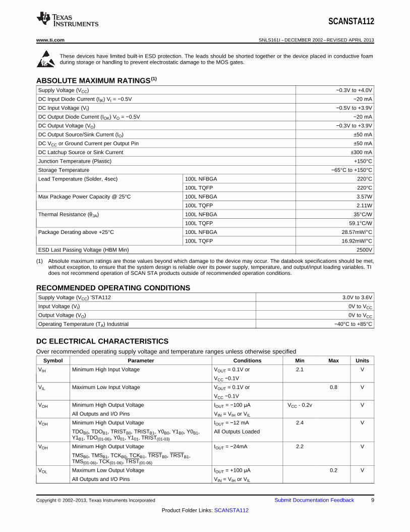
ABSOLUTE MAXIMUM RATINGS (1)
Supply Voltage (VCC) −0.3V to +4.0V
DC Input Diode Current (IIK) VI = −0.5V −20 mA
DC Input Voltage (VI) −0.5V to +3.9V
DC Output Diode Current (IOK) VO = −0.5V −20 mA
DC Output Voltage (VO) −0.3V to +3.9V
DC Output Source/Sink Current (IO) ±50 mA
DC VCC or Ground Current per Output Pin ±50 mA
DC Latchup Source or Sink Current ±300 mA
Junction Temperature (Plastic) +150°C
Storage Temperature −65°C to +150°C
Lead Temperature (Solder, 4sec) 100L NFBGA 220°C
100L TQFP 220°C
Max Package Power Capacity @ 25°C 100L NFBGA 3.57W
100L TQFP 2.11W
Thermal Resistance (θJA) 100L NFBGA 35°C/W
100L TQFP 59.1°C/W
Package Derating above +25°C 100L NFBGA 28.57mW/°C
100L TQFP 16.92mW/°C
ESD Last Passing Voltage (HBM Min) 2500V
(1) Absolute maximum ratings are those values beyond which damage to the device may occur. The databook specifications should be met,without exception, to ensure that the system design is reliable over its power supply, temperature, and output/input loading variables. TIdoes not recommend operation of SCAN STA products outside of recommended operation conditions.
RECOMMENDED OPERATING CONDITIONSSupply Voltage (VCC) 'STA112 3.0V to 3.6V
Input Voltage (VI) 0V to VCC
Output Voltage (VO) 0V to VCC
Operating Temperature (TA) Industrial −40°C to +85°C
DC ELECTRICAL CHARACTERISTICSOver recommended operating supply voltage and temperature ranges unless otherwise specified
Symbol Parameter Conditions Min Max Units
VIH Minimum High Input Voltage VOUT = 0.1V or 2.1 V
VCC −0.1V
VIL Maximum Low Input Voltage VOUT = 0.1V or 0.8 V
VCC −0.1V
VOH Minimum High Output Voltage IOUT = −100 μA VCC - 0.2v V
All Outputs and I/O Pins VIN = VIH or VIL
VOH Minimum High Output Voltage IOUT = −12 mA 2.4 V
TDOB0, TDOB1, TRISTB0, TRISTB1, Y0B0, Y1B0, Y0B1, All Outputs LoadedY1B1, TDO(01-06), Y001, Y101, TRIST(01-03)
VOH Minimum High Output Voltage IOUT = −24mA 2.2 V
TMSB0, TMSB1, TCKB0, TCKB1, TRSTB0, TRSTB1,TMS(01-06), TCK(01-06), TRST(01-06)
VOL Maximum Low Output Voltage IOUT = +100 μA 0.2 V
All Outputs and I/O Pins VIN = VIH or VIL
Copyright © 2002–2013, Texas Instruments Incorporated Submit Documentation Feedback 9
Product Folder Links: SCANSTA112
SCANSTA112
SNLS161I –DECEMBER 2002–REVISED APRIL 2013 www.ti.com
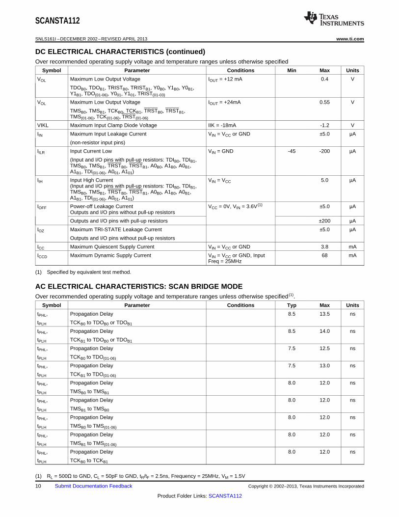
DC ELECTRICAL CHARACTERISTICS (continued)Over recommended operating supply voltage and temperature ranges unless otherwise specified
Symbol Parameter Conditions Min Max Units
VOL Maximum Low Output Voltage IOUT = +12 mA 0.4 V
TDOB0, TDOB1, TRISTB0, TRISTB1, Y0B0, Y1B0, Y0B1,Y1B1, TDO(01-06), Y001, Y101, TRIST(01-03)
VOL Maximum Low Output Voltage IOUT = +24mA 0.55 V
TMSB0, TMSB1, TCKB0, TCKB1, TRSTB0, TRSTB1,TMS(01-06), TCK(01-06), TRST(01-06)
VIKL Maximum Input Clamp Diode Voltage IIK = -18mA -1.2 V
IIN Maximum Input Leakage Current VIN = VCC or GND ±5.0 μA
(non-resistor input pins)
IILR Input Current Low VIN = GND -45 -200 µA
(Input and I/O pins with pull-up resistors: TDIB0, TDIB1,TMSB0, TMSB1, TRSTB0, TRSTB1, A0B0, A1B0, A0B1,A1B1, TDI(01-06), A001, A101)
IIH Input High Current VIN = VCC 5.0 µA(Input and I/O pins with pull-up resistors: TDIB0, TDIB1,TMSB0, TMSB1, TRSTB0, TRSTB1, A0B0, A1B0, A0B1,A1B1, TDI(01-06), A001, A101)
IOFF Power-off Leakage Current VCC = 0V, VIN = 3.6V (1) ±5.0 μAOutputs and I/O pins without pull-up resistors
Outputs and I/O pins with pull-up resistors ±200 μA
IOZ Maximum TRI-STATE Leakage Current ±5.0 μA
Outputs and I/O pins without pull-up resistors
ICC Maximum Quiescent Supply Current VIN = VCC or GND 3.8 mA
ICCD Maximum Dynamic Supply Current VIN = VCC or GND, Input 68 mAFreq = 25MHz
(1) Specified by equivalent test method.
AC ELECTRICAL CHARACTERISTICS: SCAN BRIDGE MODEOver recommended operating supply voltage and temperature ranges unless otherwise specified (1).
Symbol Parameter Conditions Typ Max Units
tPHL, Propagation Delay 8.5 13.5 ns
tPLH TCKB0 to TDOB0 or TDOB1
tPHL, Propagation Delay 8.5 14.0 ns
tPLH TCKB1 to TDOB0 or TDOB1
tPHL, Propagation Delay 7.5 12.5 ns
tPLH TCKB0 to TDO(01-06)
tPHL, Propagation Delay 7.5 13.0 ns
tPLH TCKB1 to TDO(01-06)
tPHL, Propagation Delay 8.0 12.0 ns
tPLH TMSB0 to TMSB1
tPHL, Propagation Delay 8.0 12.0 ns
tPLH TMSB1 to TMSB0
tPHL, Propagation Delay 8.0 12.0 ns
tPLH TMSB0 to TMS(01-06)
tPHL, Propagation Delay 8.0 12.0 ns
tPLH TMSB1 to TMS(01-06)
tPHL, Propagation Delay 8.0 12.0 ns
tPLH TCKB0 to TCKB1
(1) RL = 500Ω to GND, CL = 50pF to GND, tR/tF = 2.5ns, Frequency = 25MHz, VM = 1.5V
10 Submit Documentation Feedback Copyright © 2002–2013, Texas Instruments Incorporated
Product Folder Links: SCANSTA112
SCANSTA112
www.ti.com SNLS161I –DECEMBER 2002–REVISED APRIL 2013
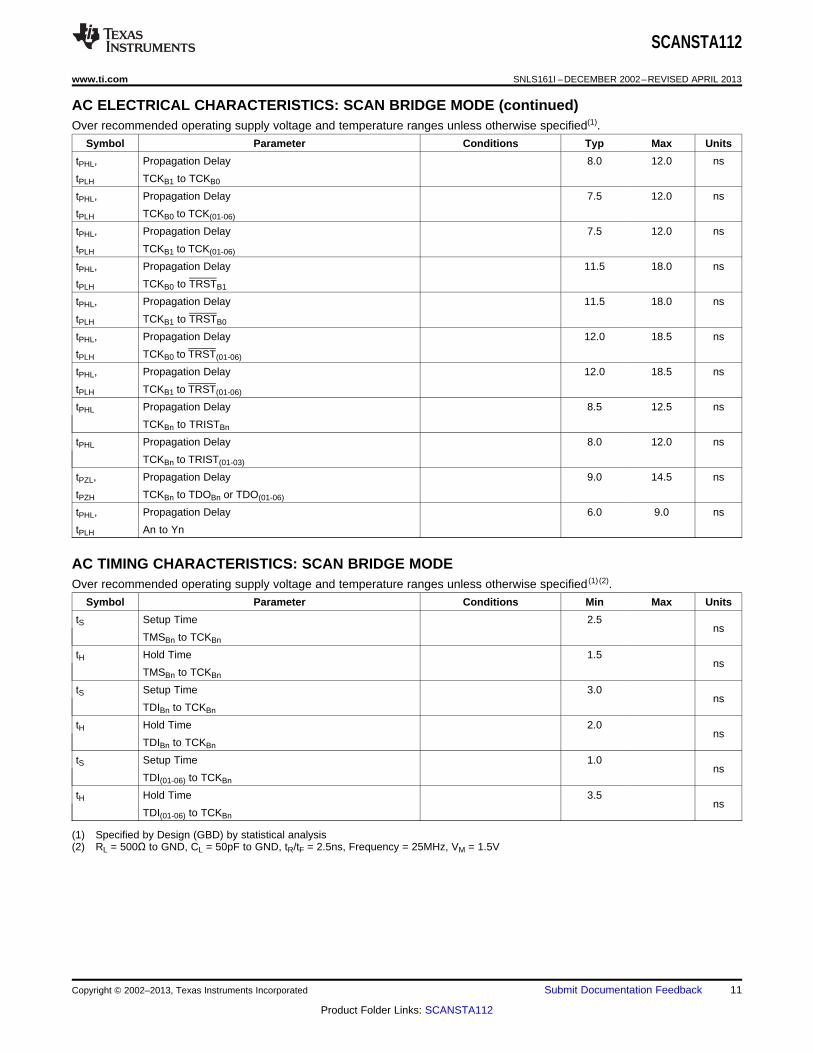
AC ELECTRICAL CHARACTERISTICS: SCAN BRIDGE MODE (continued)Over recommended operating supply voltage and temperature ranges unless otherwise specified(1).
Symbol Parameter Conditions Typ Max Units
tPHL, Propagation Delay 8.0 12.0 ns
tPLH TCKB1 to TCKB0
tPHL, Propagation Delay 7.5 12.0 ns
tPLH TCKB0 to TCK(01-06)
tPHL, Propagation Delay 7.5 12.0 ns
tPLH TCKB1 to TCK(01-06)
tPHL, Propagation Delay 11.5 18.0 ns
tPLH TCKB0 to TRSTB1
tPHL, Propagation Delay 11.5 18.0 ns
tPLH TCKB1 to TRSTB0
tPHL, Propagation Delay 12.0 18.5 ns
tPLH TCKB0 to TRST(01-06)
tPHL, Propagation Delay 12.0 18.5 ns
tPLH TCKB1 to TRST(01-06)
tPHL Propagation Delay 8.5 12.5 ns
TCKBn to TRISTBn
tPHL Propagation Delay 8.0 12.0 ns
TCKBn to TRIST(01-03)
tPZL, Propagation Delay 9.0 14.5 ns
tPZH TCKBn to TDOBn or TDO(01-06)
tPHL, Propagation Delay 6.0 9.0 ns
tPLH An to Yn
AC TIMING CHARACTERISTICS: SCAN BRIDGE MODEOver recommended operating supply voltage and temperature ranges unless otherwise specified (1) (2).
Symbol Parameter Conditions Min Max Units
tS Setup Time 2.5ns
TMSBn to TCKBn
tH Hold Time 1.5ns
TMSBn to TCKBn
tS Setup Time 3.0ns
TDIBn to TCKBn
tH Hold Time 2.0ns
TDIBn to TCKBn
tS Setup Time 1.0ns
TDI(01-06) to TCKBn
tH Hold Time 3.5ns
TDI(01-06) to TCKBn
(1) Specified by Design (GBD) by statistical analysis(2) RL = 500Ω to GND, CL = 50pF to GND, tR/tF = 2.5ns, Frequency = 25MHz, VM = 1.5V
Copyright © 2002–2013, Texas Instruments Incorporated Submit Documentation Feedback 11
Product Folder Links: SCANSTA112
SCANSTA112
SNLS161I –DECEMBER 2002–REVISED APRIL 2013 www.ti.com
AC TIMING CHARACTERISTICS: SCAN BRIDGE MODE (continued)Over recommended operating supply voltage and temperature ranges unless otherwise specified(1)(2).
Symbol Parameter Conditions Min Max Units
tREC Recovery Time 1.0ns
TCKBn from TRSTBn
tW Clock Pulse Width tR/tF = 1.0ns 10.0 ns
TCKBn(H or L)
tWL Reset Pulse Width tR/tF = 1.0ns 2.5 ns
TRSTBn(L)
FMAX Maximum Clock Frequency (3) tR/tF = 1.0ns 25 MHz
(3) When sending vectors one-way to a target device on an LSP (such as in FPGA/PLD configuration/programming), the clock frequencymay be increased above this specification. In Scan Mode (expecting to capture returning data at the LSP), the FMAX must be limited tothe above specification.
AC ELECTRICAL CHARACTERISTICS: STITCHER TRANSPARENT MODEOver recommended operating supply voltage and temperature ranges unless otherwise specified (1).
Symbol Parameter Conditions Typ Max Units
tPHL, Propagation Delay 12.5 ns
tPLH TDIB0 to TDOB1, TDIB1 to TDOB0
tPHL, Propagation Delay 12.5 ns
tPLH TDIB0 to TDO01, TDIB1 to TDO01
tPHL, Propagation Delay 12.5 ns
tPLH TDILSPn to TDOLSPn+1
tPHL, Propagation Delay 12.5 ns
tPLH TMSB0 to TMSB1, TMSB1 to TMSB0
tPHL, Propagation Delay 12.5 ns
tPLH TMSB0 to TMS(01-06), TMSB1 to TMS(01-06)
tPHL, Propagation Delay 12.5 ns
tPLH TRSTB0 to TRSTB1, TRSTB1 to TRSTB0
tPHL, Propagation Delay 12.5 ns
tPLH TRSTB0 to TRST(01-06), TRSTB1 to TRST(01-06)
(1) RL = 500Ω to GND, CL = 50pF to GND, tR/tF = 2.5ns, Frequency = 25MHz, VM = 1.5V
12 Submit Documentation Feedback Copyright © 2002–2013, Texas Instruments Incorporated
Product Folder Links: SCANSTA112
SCANSTA112
www.ti.com SNLS161I –DECEMBER 2002–REVISED APRIL 2013
TEST CIRCUIT DIAGRAMS
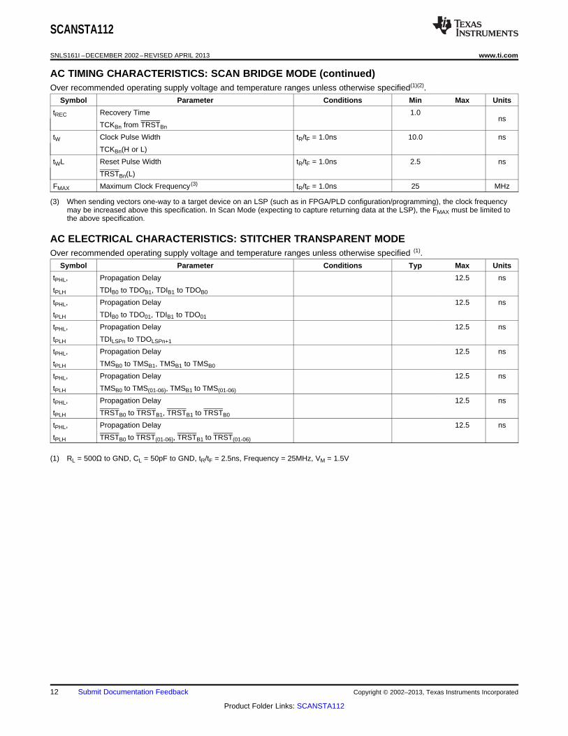
Figure 6. Waveforms for an Unparked STA112 in the Shift-DR (IR) TAP Controller State
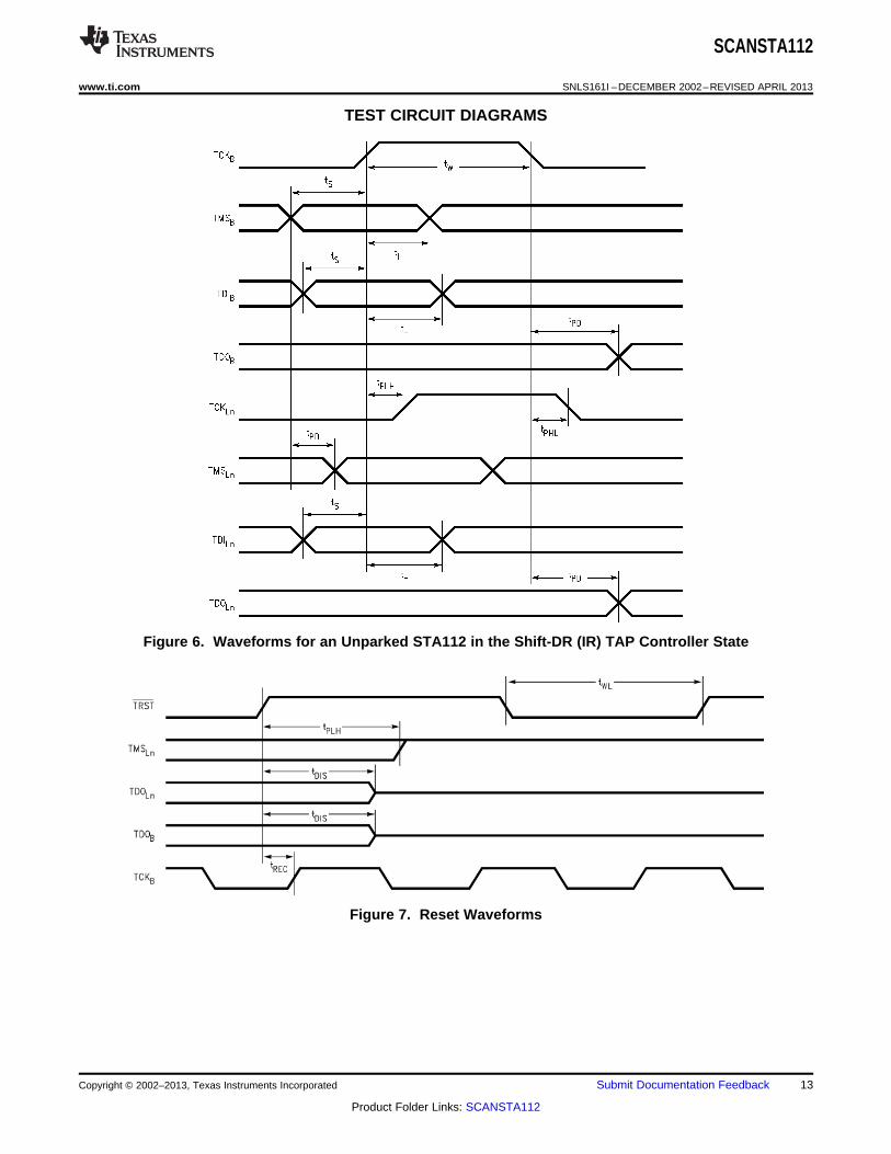
Figure 7. Reset Waveforms
Copyright © 2002–2013, Texas Instruments Incorporated Submit Documentation Feedback 13
Product Folder Links: SCANSTA112
SCANSTA112
SNLS161I –DECEMBER 2002–REVISED APRIL 2013 www.ti.com
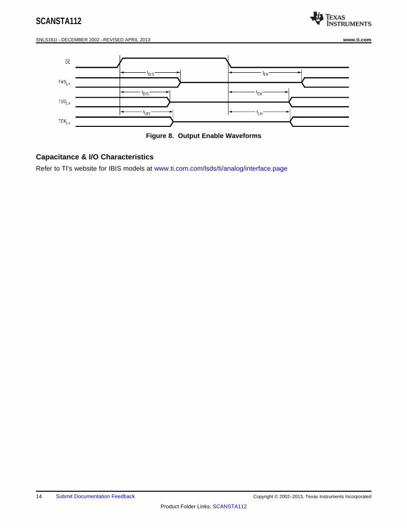
Figure 8. Output Enable Waveforms
Capacitance & I/O Characteristics
Refer to TI's website for IBIS models at www.ti.com.com/lsds/ti/analog/interface.page
14 Submit Documentation Feedback Copyright © 2002–2013, Texas Instruments Incorporated
Product Folder Links: SCANSTA112
SCANSTA112
www.ti.com SNLS161I –DECEMBER 2002–REVISED APRIL 2013
REVISION HISTORY
Changes from Revision H (April 2013) to Revision I Page
• Changed layout of National Data Sheet to TI format .......................................................................................................... 14
Copyright © 2002–2013, Texas Instruments Incorporated Submit Documentation Feedback 15
Product Folder Links: SCANSTA112
PACKAGE OPTION ADDENDUM
www.ti.com 17-Mar-2017
Addendum-Page 1
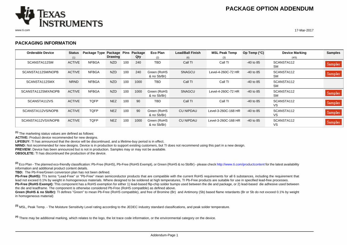
PACKAGING INFORMATION
Orderable Device Status(1)
Package Type PackageDrawing
Pins PackageQty
Eco Plan(2)
Lead/Ball Finish(6)
MSL Peak Temp(3)
Op Temp (°C) Device Marking(4/5)
Samples
SCANSTA112SM ACTIVE NFBGA NZD 100 240 TBD Call TI Call TI -40 to 85 SCANSTA112SM
SCANSTA112SM/NOPB ACTIVE NFBGA NZD 100 240 Green (RoHS& no Sb/Br)
SNAGCU Level-4-260C-72 HR -40 to 85 SCANSTA112SM
SCANSTA112SMX NRND NFBGA NZD 100 1000 TBD Call TI Call TI -40 to 85 SCANSTA112SM
SCANSTA112SMX/NOPB ACTIVE NFBGA NZD 100 1000 Green (RoHS& no Sb/Br)
SNAGCU Level-4-260C-72 HR -40 to 85 SCANSTA112SM
SCANSTA112VS ACTIVE TQFP NEZ 100 90 TBD Call TI Call TI -40 to 85 SCANSTA112VS
SCANSTA112VS/NOPB ACTIVE TQFP NEZ 100 90 Green (RoHS& no Sb/Br)
CU NIPDAU Level-3-260C-168 HR -40 to 85 SCANSTA112VS
SCANSTA112VSX/NOPB ACTIVE TQFP NEZ 100 1000 Green (RoHS& no Sb/Br)
CU NIPDAU Level-3-260C-168 HR -40 to 85 SCANSTA112VS
(1) The marketing status values are defined as follows:ACTIVE: Product device recommended for new designs.LIFEBUY: TI has announced that the device will be discontinued, and a lifetime-buy period is in effect.NRND: Not recommended for new designs. Device is in production to support existing customers, but TI does not recommend using this part in a new design.PREVIEW: Device has been announced but is not in production. Samples may or may not be available.OBSOLETE: TI has discontinued the production of the device.
(2) Eco Plan - The planned eco-friendly classification: Pb-Free (RoHS), Pb-Free (RoHS Exempt), or Green (RoHS & no Sb/Br) - please check http://www.ti.com/productcontent for the latest availabilityinformation and additional product content details.TBD: The Pb-Free/Green conversion plan has not been defined.Pb-Free (RoHS): TI's terms "Lead-Free" or "Pb-Free" mean semiconductor products that are compatible with the current RoHS requirements for all 6 substances, including the requirement thatlead not exceed 0.1% by weight in homogeneous materials. Where designed to be soldered at high temperatures, TI Pb-Free products are suitable for use in specified lead-free processes.Pb-Free (RoHS Exempt): This component has a RoHS exemption for either 1) lead-based flip-chip solder bumps used between the die and package, or 2) lead-based die adhesive used betweenthe die and leadframe. The component is otherwise considered Pb-Free (RoHS compatible) as defined above.Green (RoHS & no Sb/Br): TI defines "Green" to mean Pb-Free (RoHS compatible), and free of Bromine (Br) and Antimony (Sb) based flame retardants (Br or Sb do not exceed 0.1% by weightin homogeneous material)
(3) MSL, Peak Temp. - The Moisture Sensitivity Level rating according to the JEDEC industry standard classifications, and peak solder temperature.
(4) There may be additional marking, which relates to the logo, the lot trace code information, or the environmental category on the device.
PACKAGE OPTION ADDENDUM
www.ti.com 17-Mar-2017
Addendum-Page 2
(5) Multiple Device Markings will be inside parentheses. Only one Device Marking contained in parentheses and separated by a "~" will appear on a device. If a line is indented then it is a continuationof the previous line and the two combined represent the entire Device Marking for that device.
(6) Lead/Ball Finish - Orderable Devices may have multiple material finish options. Finish options are separated by a vertical ruled line. Lead/Ball Finish values may wrap to two lines if the finishvalue exceeds the maximum column width.
Important Information and Disclaimer:The information provided on this page represents TI's knowledge and belief as of the date that it is provided. TI bases its knowledge and belief on informationprovided by third parties, and makes no representation or warranty as to the accuracy of such information. Efforts are underway to better integrate information from third parties. TI has taken andcontinues to take reasonable steps to provide representative and accurate information but may not have conducted destructive testing or chemical analysis on incoming materials and chemicals.TI and TI suppliers consider certain information to be proprietary, and thus CAS numbers and other limited information may not be available for release.
In no event shall TI's liability arising out of such information exceed the total purchase price of the TI part(s) at issue in this document sold by TI to Customer on an annual basis.
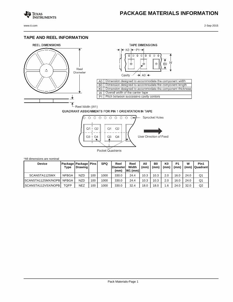
TAPE AND REEL INFORMATION
*All dimensions are nominal
Device PackageType
PackageDrawing
Pins SPQ ReelDiameter
(mm)
ReelWidth
W1 (mm)
A0(mm)
B0(mm)
K0(mm)
P1(mm)
W(mm)
Pin1Quadrant
SCANSTA112SMX NFBGA NZD 100 1000 330.0 24.4 10.3 10.3 2.0 16.0 24.0 Q1
SCANSTA112SMX/NOPB NFBGA NZD 100 1000 330.0 24.4 10.3 10.3 2.0 16.0 24.0 Q1
SCANSTA112VSX/NOPB TQFP NEZ 100 1000 330.0 32.4 18.0 18.0 1.6 24.0 32.0 Q2
PACKAGE MATERIALS INFORMATION
www.ti.com 2-Sep-2015
Pack Materials-Page 1
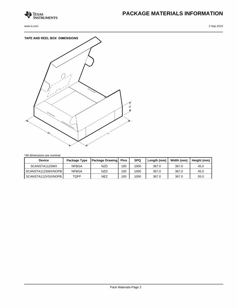
*All dimensions are nominal
Device Package Type Package Drawing Pins SPQ Length (mm) Width (mm) Height (mm)
SCANSTA112SMX NFBGA NZD 100 1000 367.0 367.0 45.0
SCANSTA112SMX/NOPB NFBGA NZD 100 1000 367.0 367.0 45.0
SCANSTA112VSX/NOPB TQFP NEZ 100 1000 367.0 367.0 55.0
PACKAGE MATERIALS INFORMATION
www.ti.com 2-Sep-2015
Pack Materials-Page 2
MECHANICAL DATA
PFD0100A
www.ti.com
VJD100A (Rev C)
TYPICAL
a0412025
Text Box
NEZ0100A
MECHANICAL DATA
NZD0100A
www.ti.com
IMPORTANT NOTICE
Texas Instruments Incorporated (TI) reserves the right to make corrections, enhancements, improvements and other changes to itssemiconductor products and services per JESD46, latest issue, and to discontinue any product or service per JESD48, latest issue. Buyersshould obtain the latest relevant information before placing orders and should verify that such information is current and complete.TI’s published terms of sale for semiconductor products (http://www.ti.com/sc/docs/stdterms.htm) apply to the sale of packaged integratedcircuit products that TI has qualified and released to market. Additional terms may apply to the use or sale of other types of TI products andservices.Reproduction of significant portions of TI information in TI data sheets is permissible only if reproduction is without alteration and isaccompanied by all associated warranties, conditions, limitations, and notices. TI is not responsible or liable for such reproduceddocumentation. Information of third parties may be subject to additional restrictions. Resale of TI products or services with statementsdifferent from or beyond the parameters stated by TI for that product or service voids all express and any implied warranties for theassociated TI product or service and is an unfair and deceptive business practice. TI is not responsible or liable for any such statements.Buyers and others who are developing systems that incorporate TI products (collectively, “Designers”) understand and agree that Designersremain responsible for using their independent analysis, evaluation and judgment in designing their applications and that Designers havefull and exclusive responsibility to assure the safety of Designers' applications and compliance of their applications (and of all TI productsused in or for Designers’ applications) with all applicable regulations, laws and other applicable requirements. Designer represents that, withrespect to their applications, Designer has all the necessary expertise to create and implement safeguards that (1) anticipate dangerousconsequences of failures, (2) monitor failures and their consequences, and (3) lessen the likelihood of failures that might cause harm andtake appropriate actions. Designer agrees that prior to using or distributing any applications that include TI products, Designer willthoroughly test such applications and the functionality of such TI products as used in such applications.TI’s provision of technical, application or other design advice, quality characterization, reliability data or other services or information,including, but not limited to, reference designs and materials relating to evaluation modules, (collectively, “TI Resources”) are intended toassist designers who are developing applications that incorporate TI products; by downloading, accessing or using TI Resources in anyway, Designer (individually or, if Designer is acting on behalf of a company, Designer’s company) agrees to use any particular TI Resourcesolely for this purpose and subject to the terms of this Notice.TI’s provision of TI Resources does not expand or otherwise alter TI’s applicable published warranties or warranty disclaimers for TIproducts, and no additional obligations or liabilities arise from TI providing such TI Resources. TI reserves the right to make corrections,enhancements, improvements and other changes to its TI Resources. TI has not conducted any testing other than that specificallydescribed in the published documentation for a particular TI Resource.Designer is authorized to use, copy and modify any individual TI Resource only in connection with the development of applications thatinclude the TI product(s) identified in such TI Resource. NO OTHER LICENSE, EXPRESS OR IMPLIED, BY ESTOPPEL OR OTHERWISETO ANY OTHER TI INTELLECTUAL PROPERTY RIGHT, AND NO LICENSE TO ANY TECHNOLOGY OR INTELLECTUAL PROPERTYRIGHT OF TI OR ANY THIRD PARTY IS GRANTED HEREIN, including but not limited to any patent right, copyright, mask work right, orother intellectual property right relating to any combination, machine, or process in which TI products or services are used. Informationregarding or referencing third-party products or services does not constitute a license to use such products or services, or a warranty orendorsement thereof. Use of TI Resources may require a license from a third party under the patents or other intellectual property of thethird party, or a license from TI under the patents or other intellectual property of TI.TI RESOURCES ARE PROVIDED “AS IS” AND WITH ALL FAULTS. TI DISCLAIMS ALL OTHER WARRANTIES ORREPRESENTATIONS, EXPRESS OR IMPLIED, REGARDING RESOURCES OR USE THEREOF, INCLUDING BUT NOT LIMITED TOACCURACY OR COMPLETENESS, TITLE, ANY EPIDEMIC FAILURE WARRANTY AND ANY IMPLIED WARRANTIES OFMERCHANTABILITY, FITNESS FOR A PARTICULAR PURPOSE, AND NON-INFRINGEMENT OF ANY THIRD PARTY INTELLECTUALPROPERTY RIGHTS. TI SHALL NOT BE LIABLE FOR AND SHALL NOT DEFEND OR INDEMNIFY DESIGNER AGAINST ANY CLAIM,INCLUDING BUT NOT LIMITED TO ANY INFRINGEMENT CLAIM THAT RELATES TO OR IS BASED ON ANY COMBINATION OFPRODUCTS EVEN IF DESCRIBED IN TI RESOURCES OR OTHERWISE. IN NO EVENT SHALL TI BE LIABLE FOR ANY ACTUAL,DIRECT, SPECIAL, COLLATERAL, INDIRECT, PUNITIVE, INCIDENTAL, CONSEQUENTIAL OR EXEMPLARY DAMAGES INCONNECTION WITH OR ARISING OUT OF TI RESOURCES OR USE THEREOF, AND REGARDLESS OF WHETHER TI HAS BEENADVISED OF THE POSSIBILITY OF SUCH DAMAGES.Unless TI has explicitly designated an individual product as meeting the requirements of a particular industry standard (e.g., ISO/TS 16949and ISO 26262), TI is not responsible for any failure to meet such industry standard requirements.Where TI specifically promotes products as facilitating functional safety or as compliant with industry functional safety standards, suchproducts are intended to help enable customers to design and create their own applications that meet applicable functional safety standardsand requirements. Using products in an application does not by itself establish any safety features in the application. Designers mustensure compliance with safety-related requirements and standards applicable to their applications. Designer may not use any TI products inlife-critical medical equipment unless authorized officers of the parties have executed a special contract specifically governing such use.Life-critical medical equipment is medical equipment where failure of such equipment would cause serious bodily injury or death (e.g., lifesupport, pacemakers, defibrillators, heart pumps, neurostimulators, and implantables). Such equipment includes, without limitation, allmedical devices identified by the U.S. Food and Drug Administration as Class III devices and equivalent classifications outside the U.S.TI may expressly designate certain products as completing a particular qualification (e.g., Q100, Military Grade, or Enhanced Product).Designers agree that it has the necessary expertise to select the product with the appropriate qualification designation for their applicationsand that proper product selection is at Designers’ own risk. Designers are solely responsible for compliance with all legal and regulatoryrequirements in connection with such selection.Designer will fully indemnify TI and its representatives against any damages, costs, losses, and/or liabilities arising out of Designer’s non-compliance with the terms and provisions of this Notice.
Mailing Address: Texas Instruments, Post Office Box 655303, Dallas, Texas 75265Copyright © 2017, Texas Instruments Incorporated
Related Documents