S6B0108 64CH SEGMENT DRIVER FOR DOT MATRIX LCD July. 2001 Ver. 0.0 Contents in this document are subject to change without notice. No part of this document may be reproduced or transmitted in any form or by any means, electronic or mechanical, for any purpose, without the express written permission of LCD Driver IC Team. Precautions for Light Light has characteristics to move electrons in the integrated circuitry of semiconductors, therefore may change the characteristics of semiconductor devices when irradiated with light. Consequently, the users of the packages which may expose chips to external light such as COB, COG, TCP and COF must consider effective methods to block out light from reaching the IC on all parts of the surface area, the top, bottom and the sides of the chip. Follow the precautions below when using the products. 1. Consider and verify the protection of penetrating light to the IC at substrate ( board or glass) or product design stage. 2. Always test and inspect products under the environment with no penetration of light.

Welcome message from author
This document is posted to help you gain knowledge. Please leave a comment to let me know what you think about it! Share it to your friends and learn new things together.
Transcript
S6B0108
64CH SEGMENT DRIVER FOR DOT MATRIX LCD
July. 2001
Ver. 0.0
Contents in this document are subject to change without notice. No part of this document may be reproduced or transmitted in any form or by any means, electronic or mechanical, for any purpose, without the express written permission of LCD Driver IC Team.
Precautions for Light
Light has characteristics to move electrons in the integrated circuitry of semiconductors, therefore may change the characteristics of semiconductor devices when irradiated with light. Consequently, the users of the packages which may expose chips to external light such as COB, COG, TCP and COF must consider effective methods to block out light from reaching the IC on all parts of the surface area, the top, bottom and the sides of the chip. Follow the precautions below when using the products.
1. Consider and verify the protection of penetrating light to the IC at substrate (board or glass) or product design stage.
2. Always test and inspect products under the environment with no penetration of light.
S6B0108 64CH SEGMENT DRIVER FOR DOT MATRIX LCD
2
S6B0755 Specification Revision History
Version Content Date
0.0 Original July.2001
S6B0108 64CH SEGMENT DRIVER FOR DOT MATRIX LCD
3
CONTENTS
INTRODUCTION ............................................................................................................................................. 1
BLOCK DIAGRAM .......................................................................................................................................... 2
PIN CONFIGURATION .................................................................................................................................... 3
100 QFP.................................................................................................................................................. 3
PAD DIAGRAM (CHIP LAYOUT FOR THE 100QFP).................................................................................... 4
PAD CENTER COORDINATES (100QFP).................................................................................................. 5
100TQFP (S6B2108)................................................................................................................................. 6
PAD DIAGRAM (CHIP LAYOUT FOR THE 100TQFP).................................................................................. 7
PAD CENTER COORDINATES (100TQFP- S6B2108).................................................................................. 8
PIN DESCRIPTION ........................................................................................................................................ 9
MAXIMUM ABSOLUTE LIMIT ......................................................................................................................11
ELECTRICAL CHARACTERISTICS ................................................................................................................12
DC CHARACTERISTICS ..........................................................................................................................12
AC CHARACTERISTICS (VDD = +5V ± 10%, VSS = 0V, Ta =-30 to +85°C) ..................................................13
OPERATING PRINCIPLES AND METHODS ....................................................................................................17
I/O BUFFER ...........................................................................................................................................17
RESET...................................................................................................................................................18
DISPLAY CONTROL INSTRUCTION.............................................................................................................21
DISPLAY ON/OFF...................................................................................................................................22
STATUS READ.......................................................................................................................................23
APPLICATION CIRCUIT................................................................................................................................24
1/64 DUTY COMMON DRIVER (S6B0107) INTERFACE CIRCUIT ................................................................24
TIMING DIAGRAM (1/64 DUTY)................................................................................................................25
LCD PANEL INTERFACE APPLICATION CIRCUIT .....................................................................................26

64CH SEGMENT DRIVER FOR DOT MATRIX LCD S6B0108
1
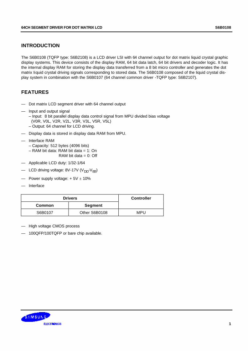
INTRODUCTION
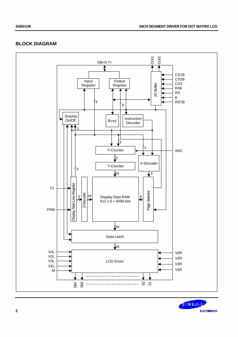
The S6B0108 (TQFP type: S6B2108) is a LCD driver LSI with 64 channel output for dot matrix liquid crystal graphic display systems. This device consists of the display RAM, 64 bit data latch, 64 bit drivers and decoder logic. It has the internal display RAM for storing the display data transferred from a 8 bit micro controller and generates the dot matrix Iiquid crystal driving signals corresponding to stored data. The S6B0108 composed of the liquid crystal dis-play system in combination with the S6B0107 (64 channel common driver -TQFP type: S6B2107).
FEATURES
— Dot matrix LCD segment driver with 64 channel output
— Input and output signal – Input: 8 bit parallel display data control signal from MPU divided bias voltage (V0R, V0L, V2R, V2L, V3R, V3L, V5R, V5L) – Output: 64 channel for LCD driving.
— Display data is stored in display data RAM from MPU.
— Interface RAM – Capacity: 512 bytes (4096 bits) – RAM bit data: RAM bit data = 1: On RAM bit data = 0: Off
— Applicable LCD duty: 1/32-1/64
— LCD driving voltage: 8V-17V (VDD-VEE)
— Power supply voltage: + 5V ± 10%
— Interface
Drivers Controller
Common Segment
S6B0107 Other S6B0108 MPU
— High voltage CMOS process
— 100QFP/100TQFP or bare chip available.
S6B0108 64CH SEGMENT DRIVER FOR DOT MATRIX LCD
2
BLOCK DIAGRAM
S64
S63
InstructionDecoder
LCD Driver
Data Latch
DisplayOn/Off
I/O B
uffe
r
88
6
3
6
S2 S1
V5R
V3R
V2RV0R
MV5LV3LV2LV0L
FRM
CL
ADC
RSTBERSR/WCS3CS2BCS1B
CLK
2
CLK
1
DB<0:7>
InputRegister
OutputRegister
Busy
Y-Counter
Y-CounterX-Decoder
6 64
1
6
64
64
64
8
8
Display Data RAM512 x 8 = 4096 bits
Dis
play
Sta
rt Li
ne R
egis
ter
Z-D
ecod
er
Page
Sel
ecto
r
64CH SEGMENT DRIVER FOR DOT MATRIX LCD S6B0108
3
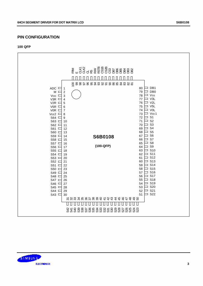
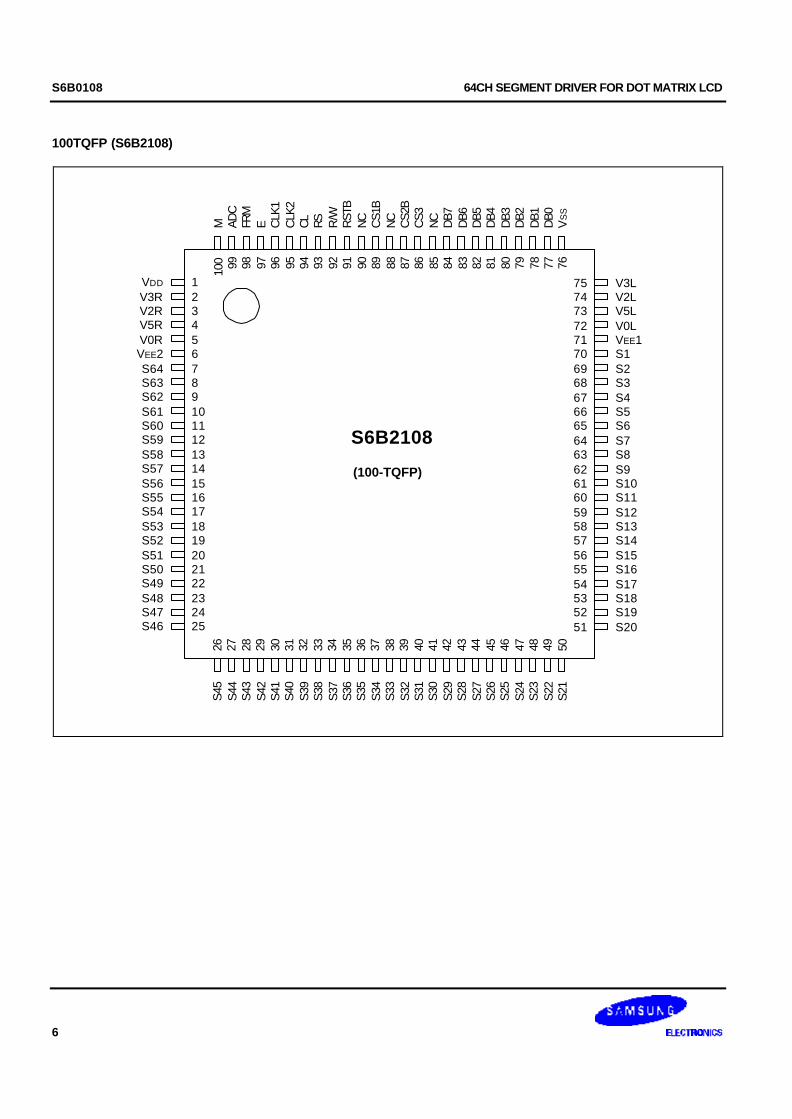
PIN CONFIGURATION
100 QFP
S6B0108
(100-QFP)
123456789101112131415161718192021222324252627282930
807978777675747372717069686766656463626160595857565554535251
31 32 33 34 35 36 37 38 39 40 41 42 43 44 45 46 47 48 49 50
100 99 98 97 96 95 94 93 92 91 90 86 85 84 83 82 81
ADCM
VDD
V3RV2RV5RV0R
VEE2S64S63S62S61S60S59S58S57S56S55S54S53S52S51S50S49S48S47S46S45S44S43
FRM
E CLK
1C
LK2
CL RS R/W
RST
BC
S1B
CS2
BC
S3D
B7D
B6D
B5D
B4D
B3D
B2
S42
S41
S40
S39
S38
S37
S36
S35
S34
S33
S32
S31
S30
S29
S28
S27
S26
S25
S24
S23
DB1DB0VSS
V3LV2LV5LV0LVEE1S1S2S3S4S5S6S7S8S9S10S11S12S13S14S15S16S17S18S19S20S21S22
S6B0108 64CH SEGMENT DRIVER FOR DOT MATRIX LCD
4
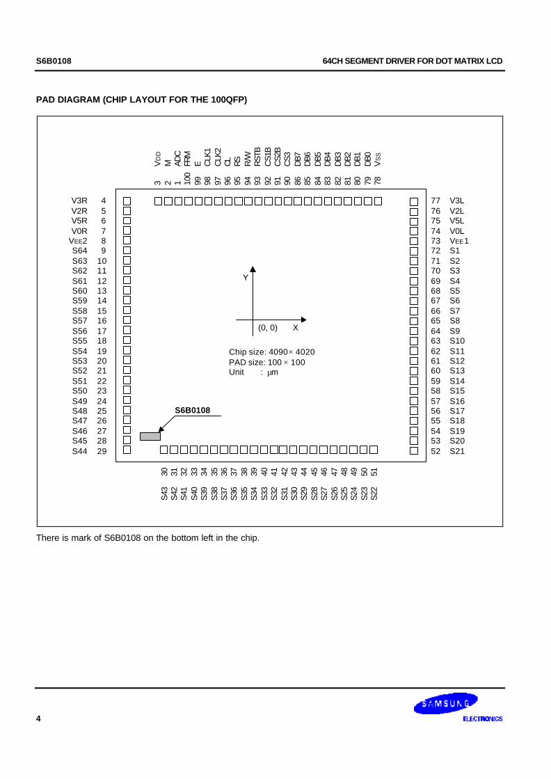
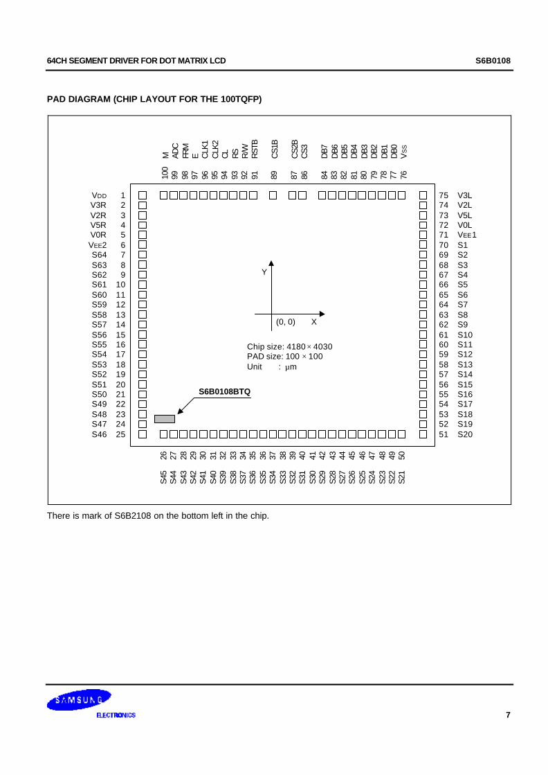
PAD DIAGRAM (CHIP LAYOUT FOR THE 100QFP)
3 2 1 100
99 98 97 96 95 94 93 92 91 90 86 85 84 83 82 81 80 79 78
VD
D
M ADC
FRM
E CLK
1C
LK2
CL RS R/W
RST
BC
S1B
CS2
BC
S3D
B7D
B6D
B5D
B4D
B3D
B2D
B1D
B0V
SS
456789
1011121314151617181920212223242526272829
V3RV2RV5RV0R
VEE2S64S63S62S61S60S59S58S57S56S55S54S53S52S51S50S49S48S47S46S45S44
Chip size: 4090 × 4020PAD size: 100 × 100Unit : µm
(0, 0) X
Y
S6B0108
7776757473727170696867666564636261605958575655545352
V3LV2LV5LV0LVEE1S1S2S3S4S5S6S7S8S9S10S11S12S13S14S15S16S17S18S19S20S21
30 31 32 33 34 35 36 37 38 39 40 41 42 43 44 45 46 47 48 49 50 51
S43
S42
S41
S40
S39
S38
S37
S36
S35
S34
S33
S32
S31
S30
S29
S28
S27
S26
S25
S24
S23
S22
There is mark of S6B0108 on the bottom left in the chip.
64CH SEGMENT DRIVER FOR DOT MATRIX LCD S6B0108
5
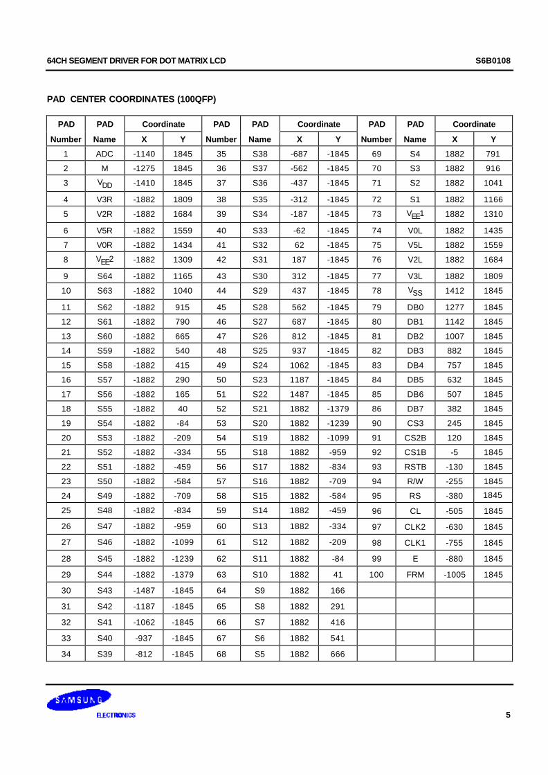
PAD CENTER COORDINATES (100QFP)
PAD PAD Coordinate PAD PAD Coordinate PAD PAD Coordinate
Number Name X Y Number Name X Y Number Name X Y
1 ADC -1140 1845 35 S38 -687 -1845 69 S4 1882 791
2 M -1275 1845 36 S37 -562 -1845 70 S3 1882 916
3 VDD -1410 1845 37 S36 -437 -1845 71 S2 1882 1041
4 V3R -1882 1809 38 S35 -312 -1845 72 S1 1882 1166
5 V2R -1882 1684 39 S34 -187 -1845 73 VEE1 1882 1310
6 V5R -1882 1559 40 S33 -62 -1845 74 V0L 1882 1435
7 V0R -1882 1434 41 S32 62 -1845 75 V5L 1882 1559
8 VEE2 -1882 1309 42 S31 187 -1845 76 V2L 1882 1684
9 S64 -1882 1165 43 S30 312 -1845 77 V3L 1882 1809
10 S63 -1882 1040 44 S29 437 -1845 78 VSS 1412 1845
11 S62 -1882 915 45 S28 562 -1845 79 DB0 1277 1845
12 S61 -1882 790 46 S27 687 -1845 80 DB1 1142 1845
13 S60 -1882 665 47 S26 812 -1845 81 DB2 1007 1845
14 S59 -1882 540 48 S25 937 -1845 82 DB3 882 1845
15 S58 -1882 415 49 S24 1062 -1845 83 DB4 757 1845
16 S57 -1882 290 50 S23 1187 -1845 84 DB5 632 1845
17 S56 -1882 165 51 S22 1487 -1845 85 DB6 507 1845
18 S55 -1882 40 52 S21 1882 -1379 86 DB7 382 1845
19 S54 -1882 -84 53 S20 1882 -1239 90 CS3 245 1845
20 S53 -1882 -209 54 S19 1882 -1099 91 CS2B 120 1845
21 S52 -1882 -334 55 S18 1882 -959 92 CS1B -5 1845
22 S51 -1882 -459 56 S17 1882 -834 93 RSTB -130 1845
23 S50 -1882 -584 57 S16 1882 -709 94 R/W -255 1845
24 S49 -1882 -709 58 S15 1882 -584 95 RS -380 1845
25 S48 -1882 -834 59 S14 1882 -459 96 CL -505 1845
26 S47 -1882 -959 60 S13 1882 -334 97 CLK2 -630 1845
27 S46 -1882 -1099 61 S12 1882 -209 98 CLK1 -755 1845
28 S45 -1882 -1239 62 S11 1882 -84 99 E -880 1845
29 S44 -1882 -1379 63 S10 1882 41 100 FRM -1005 1845
30 S43 -1487 -1845 64 S9 1882 166
31 S42 -1187 -1845 65 S8 1882 291
32 S41 -1062 -1845 66 S7 1882 416
33 S40 -937 -1845 67 S6 1882 541
34 S39 -812 -1845 68 S5 1882 666
S6B0108 64CH SEGMENT DRIVER FOR DOT MATRIX LCD
6
100TQFP (S6B2108)
VDD
V3RV2RV5RV0RVEE2S64S63S62S61S60S59S58S57S56S55S54S53S52S51S50S49S48S47S46
S6B2108
(100-TQFP)
12345678910111213141516171819202122232425
75747372717069686766656463626160595857565554535251
26 27 28 29 30 31 32 33 34 35 36 37 38 39 40 41 42 43 44 45 46 47 48 49 50
100 99 98 97 96 95 94 93 92 91 90 89 88 87 86 85 84 83 82 81 80 79 78 77 76
M ADC
FRM
E CLK
1C
LK2
CL RS R/W
RST
BNC C
S1B
NC CS2
BC
S3NC D
B7D
B6D
B5D
B4D
B3D
B2D
B1D
B0V
SS
S45
S44
S43
S42
S41
S40
S39
S38
S37
S36
S35
S34
S33
S32
S31
S30
S29
S28
S27
S26
S25
S24
S23
S22
S21
V3LV2LV5LV0LVEE1S1S2S3S4S5S6S7S8S9S10S11S12S13S14S15S16S17S18S19S20
64CH SEGMENT DRIVER FOR DOT MATRIX LCD S6B0108
7
PAD DIAGRAM (CHIP LAYOUT FOR THE 100TQFP)
75747372717069686766656463626160595857565554535251
26 27 28 29 30 31 32 33 34 35 36 37 38 39 40 41 42 43 44 45 46 47 48 49 50
100
99 98 97 96 95 94 93 92 91 89 87 86 84 83 82 81 80 79 78 77 76
M ADC
FRM
E CLK
1C
LK2
CL RS R/W
RST
B
CS1
B
CS2
BC
S3
DB7
DB6
DB5
DB4
DB3
DB2
DB1
DB0
VS
S
S45
S44
S43
S42
S41
S40
S39
S38
S37
S36
S35
S34
S33
S32
S31
S30
S29
S28
S27
S26
S25
S24
S23
S22
S21
V3LV2LV5LV0LVEE1S1S2S3S4S5S6S7S8S9S10S11S12S13S14S15S16S17S18S19S20
123456789
10111213141516171819202122232425
VDD
V3RV2RV5RV0RVEE2S64S63S62S61S60S59S58S57S56S55S54S53S52S51S50S49S48S47S46
Chip size: 4180 × 4030PAD size: 100 × 100Unit : µm
(0, 0) X
Y
S6B0108BTQ
There is mark of S6B2108 on the bottom left in the chip.
S6B0108 64CH SEGMENT DRIVER FOR DOT MATRIX LCD
8
PAD CENTER COORDINATES (100TQFP- S6B2108)
PAD PAD Coordinate PAD PAD Coordinate PAD PAD Coordinate
Number Name X Y Number Name X Y Number Name X Y
1 VDD -1924 1812.5 36 S35 -301.1 -1849 71 VEE 1924 1312.5
2 V3 -1924 1687.5 37 S34 -173.9 -1849 72 V0 1924 1437.5
3 V2 -1924 1562.5 38 S33 -46.7 -1849 73 V5 1924 1562.5
4 V5 -1924 1437.5 39 S32 80.5 -1849 74 V2 1924 1687.5
5 V0 -1924 1312.5 40 S31 207.7 -1849 75 V3 1924 1812.5
6 VEE -1924 1187.5 41 S30 334.9 -1849 76 VSS 1450.5 1849
7 S64 -1924 1033.2 42 S29 462.1 -1849 77 DB0 1315.5 1849
8 S63 -1924 906 43 S28 589.3 -1849 78 DB1 1180.5 1849
9 S62 -1924 778.8 44 S27 716.5 -1849 79 DB2 1045.5 1849
10 S61 -1924 651.6 45 S26 843.7 -1849 80 DB3 920.5 1849
11 S60 -1924 524.4 46 S25 970.9 -1849 81 DB4 795.5 1849
12 S59 -1924 397.2 47 S24 1098.1 -1849 82 DB5 670.5 1849
13 S58 -1924 270 48 S23 1225.3 -1849 83 DB6 545.5 1849
14 S57 -1924 142.8 49 S22 1352.5 -1849 84 DB7 420.5 1849
15 S56 -1924 15.6 50 S21 1479.7 -1849 85 NC
16 S55 -1924 -111.6 51 S20 1924 -1245.3 86 CS3 282.8 1849
17 S54 -1924 -238.8 52 S19 1924 -1118.1 87 CS2B 157.8 1849
18 S53 -1924 -366 53 S18 1924 -990.9 88 NC
19 S52 -1924 -493.2 54 S17 1924 -863.7 89 CS1B 32.8 1849
20 S51 -1924 -620.4 55 S16 1924 -736.5 90 NC
21 S50 -1924 -747.6 56 S15 1924 -609.3 91 RSTB -92.2 1849
22 S49 -1924 -874.8 57 S14 1924 -482.1 92 RW -217.2 1849
23 S48 -1924 -1002 58 S13 1924 -354.9 93 RS -342.2 1849
24 S47 -1924 -1129.2 59 S12 1924 -227.7 94 CL 467.2 1849
25 S46 -1924 -1256.4 60 S11 1924 -100.5 95 CLK2 -592.2 1849
26 S45 -1573.1 -1849 61 S10 1924 26.7 96 CLK1 -717.2 1849
27 S44 -1445.9 -1849 62 S9 1924 153.9 97 E -842.2 1849
28 S43 -1318.7 -1849 63 S8 1924 281.1 98 FRW -967.2 1849
29 S42 -1191.5 -1849 64 S7 1924 408.3 99 ADC -1177.8 1849
30 S41 -1064.3 -1849 65 S6 1924 535.5 100 M -1312.8 1849
31 S40 -937.1 -1849 66 S5 1924 662.7
32 S39 -809.9 -1849 67 S4 1924 789.9
33 S38 -682.7 -1849 68 S3 1924 917.1
34 S37 -555.5 -1849 69 S2 1924 1044.3
35 S36 -428.3 -1849 70 S1 1924 1171.5
64CH SEGMENT DRIVER FOR DOT MATRIX LCD S6B0108
9
PIN DESCRIPTION
Table 1. Pin Description
Pin Number QFP(TQFP)
Symbol Input/Output Description
3(1) 78(76) 73(71), 8(6)
VDD VSS
VEE1.2
Power
For internal logic circuit (+5V ± 10%) GND (0V) For LCD driver circuit VSS = 0V, VDD = +5V ± 10%, VDD-VEE = 8V - 17V VEE1 and VEE2 is connected by the same voltage.
74(72), 7(5) 76(74), 5(3) 77(75), 4(2) 75(73), 6(4)
V0L, V0R V2L, V2R V3L, V3R V5L, V5R
Power
Bias supply voltage terminals to drive the LCD.
Select Level
V0L(R), V5L(R)
Non-Select Level
V2L(R), V3L(R)
V0L and V0R (V2L & V2R, V3L & V3R, V5L & V5R) should be connected by the same voltage.
92(89) 91(87) 90(86)
CS1B CS2B CS3
Input Chip selection In order to interface data for input or output, the terminals have to be CS1B = L, CS2B = L, and CS3 = H.
2(100) M Input Alternating signal input for LCD driving.
1(99) ADC Input Address control signal to determine the relation between Y address of display RAM and terminals from which the data is output. ADC = H → Y0: S1 - Y63: S64 ADC = L → Y0: S64 - Y63: S1
100(98) FRM Input Synchronous control signal. Presets the 6-bit Z counter and synchronizes the common signal with the frame signal when the frame signal becomes high.
99(97) E Input Enable signal. Write mode (R/W = L) → data of DB<0:7> is latched at the falling edge of E. Read mode (R/W = H) → DB<0:7> appears the reading data while E is at high level.
98(96) 97(95)
CLK1 CLK2
Input 2 phase clock signal for internal operation. Used to execute operations for input/output of display RAM data and others.
96(94) CL Input Display synchronous signal. Display data is latched at rising time of the CL signal and increments the Z-address counter at the CL falling time.
95(93) RS Input Data or Instruction. RS = H → DB<0:7>: Display RAM data RS = L → DB<0:7>: Instruction data
S6B0108 64CH SEGMENT DRIVER FOR DOT MATRIX LCD
10
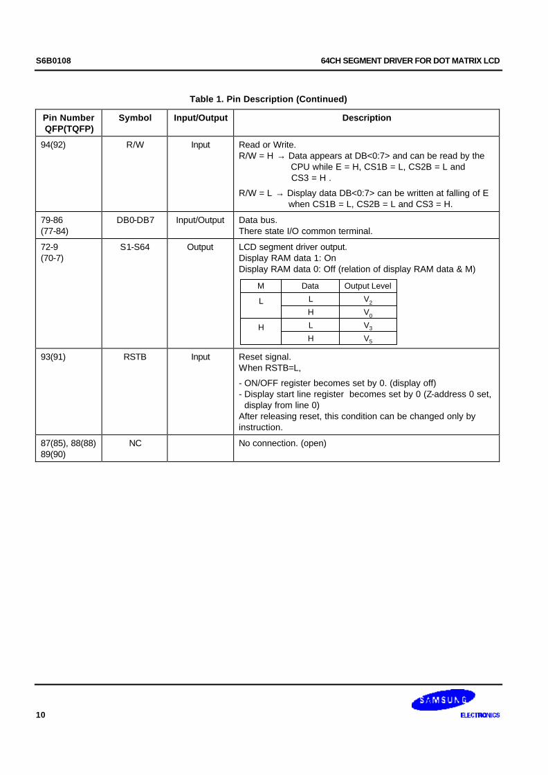
Table 1. Pin Description (Continued)
Pin Number QFP(TQFP)
Symbol Input/Output Description
94(92) R/W Input Read or Write. R/W = H → Data appears at DB<0:7> and can be read by the CPU while E = H, CS1B = L, CS2B = L and CS3 = H .
R/W = L → Display data DB<0:7> can be written at falling of E when CS1B = L, CS2B = L and CS3 = H.
79-86 (77-84)
DB0-DB7 Input/Output Data bus. There state I/O common terminal.
72-9 (70-7)
S1-S64 Output LCD segment driver output. Display RAM data 1: On Display RAM data 0: Off (relation of display RAM data & M)
M
L
Data
L
H
Output Level
L
H
H
V2
V0
V3
V5 93(91) RSTB Input Reset signal.
When RSTB=L,
- ON/OFF register becomes set by 0. (display off) - Display start line register becomes set by 0 (Z-address 0 set, display from line 0) After releasing reset, this condition can be changed only by instruction.
87(85), 88(88) 89(90)
NC No connection. (open)
64CH SEGMENT DRIVER FOR DOT MATRIX LCD S6B0108
11
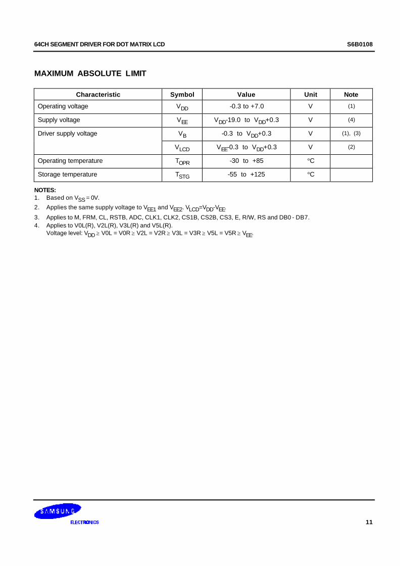
MAXIMUM ABSOLUTE LIMIT
Characteristic Symbol Value Unit Note
Operating voltage VDD -0.3 to +7.0 V (1)
Supply voltage VEE VDD-19.0 to VDD+0.3 V (4)
Driver supply voltage VB -0.3 to VDD+0.3 V (1), (3)
VLCD VEE-0.3 to VDD+0.3 V (2)
Operating temperature TOPR -30 to +85 °C
Storage temperature TSTG -55 to +125 °C
NOTES: 1. Based on VSS = 0V.
2. Applies the same supply voltage to VEE1 and VEE2. VLCD=VDD-VEE.
3. Applies to M, FRM, CL, RSTB, ADC, CLK1, CLK2, CS1B, CS2B, CS3, E, R/W, RS and DB0 - DB7. 4. Applies to V0L(R), V2L(R), V3L(R) and V5L(R). Voltage level: VDD ≥ V0L = V0R ≥ V2L = V2R ≥ V3L = V3R ≥ V5L = V5R ≥ VEE.
S6B0108 64CH SEGMENT DRIVER FOR DOT MATRIX LCD
12
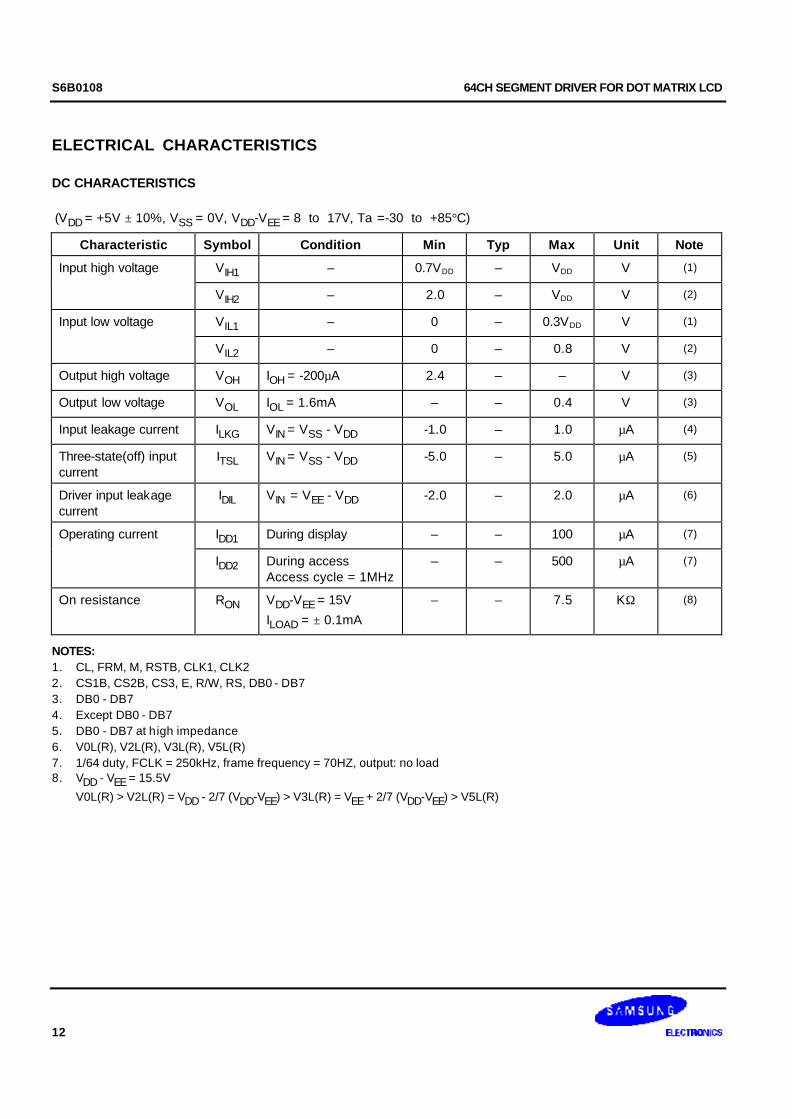
ELECTRICAL CHARACTERISTICS
DC CHARACTERISTICS
(VDD = +5V ± 10%, VSS = 0V, VDD-VEE = 8 to 17V, Ta =-30 to +85°C)
Characteristic Symbol Condition Min Typ Max Unit Note
Input high voltage VIH1 – 0.7VDD – VDD V (1)
VIH2 – 2.0 – VDD V (2)
Input low voltage VIL1 – 0 – 0.3VDD V (1)
VIL2 – 0 – 0.8 V (2)
Output high voltage VOH IOH = -200µA 2.4 – – V (3)
Output low voltage VOL IOL = 1.6mA – – 0.4 V (3)
Input leakage current ILKG VIN = VSS - VDD -1.0 – 1.0 µA (4)
Three-state(off) input current
ITSL VIN = VSS - VDD -5.0 – 5.0 µA (5)
Driver input leakage current
IDIL VIN = VEE - VDD -2.0 – 2.0 µA (6)
Operating current IDD1 During display – – 100 µA (7)
IDD2 During access Access cycle = 1MHz
– – 500 µA (7)
On resistance RON VDD-VEE = 15V ILOAD = ± 0.1mA
– – 7.5 KΩ (8)
NOTES: 1. CL, FRM, M, RSTB, CLK1, CLK2 2. CS1B, CS2B, CS3, E, R/W, RS, DB0 - DB7 3. DB0 - DB7 4. Except DB0 - DB7 5. DB0 - DB7 at high impedance 6. V0L(R), V2L(R), V3L(R), V5L(R) 7. 1/64 duty, FCLK = 250kHz, frame frequency = 70HZ, output: no load 8. VDD - VEE = 15.5V
V0L(R) > V2L(R) = VDD - 2/7 (VDD-VEE) > V3L(R) = VEE + 2/7 (VDD-VEE) > V5L(R)
64CH SEGMENT DRIVER FOR DOT MATRIX LCD S6B0108
13
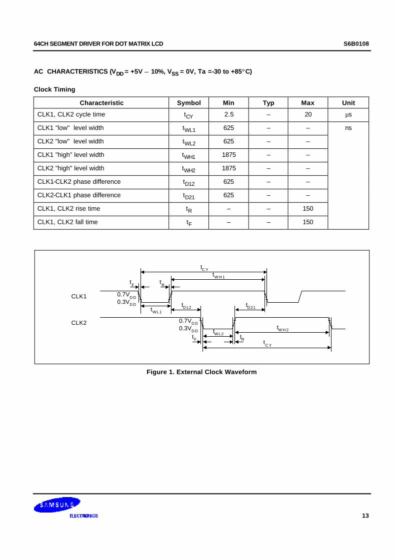
AC CHARACTERISTICS (VDD = +5V ± 10%, VSS = 0V, Ta =-30 to +85°C)
Clock Timing
Characteristic Symbol Min Typ Max Unit
CLK1, CLK2 cycle time tCY 2.5 – 20 µs
CLK1 "low" level width tWL1 625 – – ns
CLK2 "low" level width tWL2 625 – –
CLK1 "high" level width tWH1 1875 – –
CLK2 "high" level width tWH2 1875 – –
CLK1-CLK2 phase difference tD12 625 – –
CLK2-CLK1 phase difference tD21 625 – –
CLK1, CLK2 rise time tR – – 150
CLK1, CLK2 fall time tF – – 150
CLK1
CLK2
tC YtW H 1
tF
tR
tWL1
tD12 tD21
tWL2tF tR
tW H 2
tC Y
0.7VD D
0.3VD D
0.7VD D0.3VD D
Figure 1. External Clock Waveform
S6B0108 64CH SEGMENT DRIVER FOR DOT MATRIX LCD
14
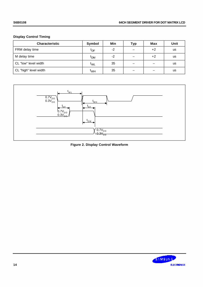
Display Control Timing
Characteristic Symbol Min Typ Max Unit
FRM delay time tDF -2 – +2 us
M delay time tDM -2 – +2 us
CL "low" level width tWL 35 – – us
CL "high" level width tWH 35 – – us
0.7VD D0.3VD D
tW L
0.7VD D0.3VD D
tD F tD F
tW H
tD M
0.7VD D0.3VD D
Figure 2. Display Control Waveform
64CH SEGMENT DRIVER FOR DOT MATRIX LCD S6B0108
15
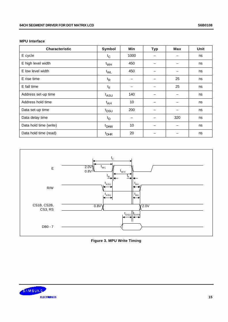
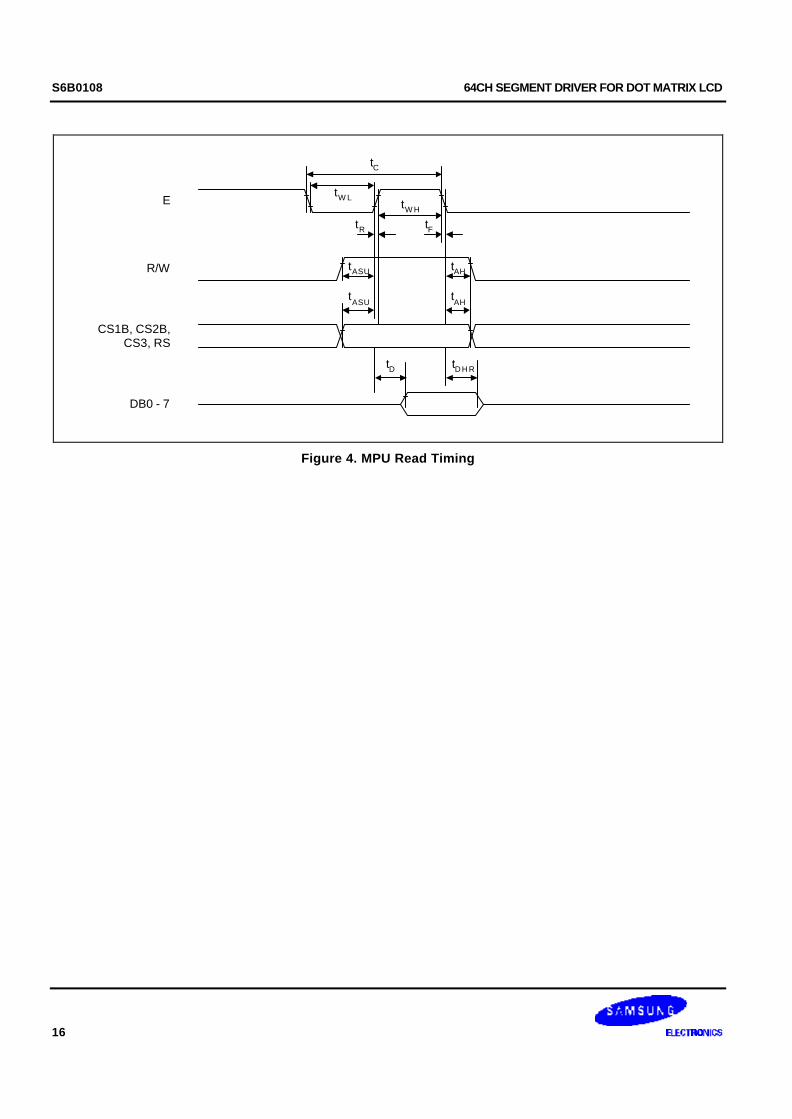
MPU Interface
Characteristic Symbol Min Typ Max Unit
E cycle tC 1000 – – ns
E high level width tWH 450 – – ns
E low level width tWL 450 – – ns
E rise time tR – – 25 ns
E fall time tF – – 25 ns
Address set-up time tASU 140 – – ns
Address hold time tAH 10 – – ns
Data set-up time tDSU 200 – – ns
Data delay time tD – – 320 ns
Data hold time (write) tDHW 10 – – ns
Data hold time (read) tDHR 20 – – ns
E
R/W
CS1B, CS2B,CS3, RS
DB0 - 7
tC
tW LtW H
tR tF
tAHtASU
tASU tAH
0.8V 2.0V
tDSU tD H W
2.0V0.8V
Figure 3. MPU Write Timing
S6B0108 64CH SEGMENT DRIVER FOR DOT MATRIX LCD
16
E
R/W
CS1B, CS2B,CS3, RS
DB0 - 7
tC
tW LtW H
tR tF
tAHtASU
tASU
tAH
tD tD H R
Figure 4. MPU Read Timing
64CH SEGMENT DRIVER FOR DOT MATRIX LCD S6B0108
17
OPERATING PRINCIPLES AND METHODS
I/O BUFFER
Input buffer controls the status between the enable and disable of chip. Unless the CS1B to CS3 is in active mode, Input or output of data and instruction does not execute. Therefore internal state is not change. But RSTB and ADC can operate regardless CS1B-CS3.
INPUT REGISTER
Input register is provided to interface with MPU which is different operating frequency. Input register stores the data temporarily before writing it into display RAM. When CS1B to CS3 are in the active mode, R/W and RS select the input register. The data from MPU is written into input register. Then Writing it into display RAM. Data latched for falling of the E signal and write automatically into the display data RAM by internal operation.
OUTPUT REGISTER
Output register stores the data temporarily from display data RAM when CS1B, CS2B and CS3 are in active mode and R/W and RS = H, stored data in display data RAM is latched in output register. When CS1B to CS3 is in active mode and R/W = H, RS = L, status data (busy check) can read out. To read the contents of display data RAM, twice access of read instruction is needed. In first access, data in display data RAM is latched into output register. In second access, MPU can read data which is latched. That is, to read the data in display data RAM, it needs dummy read. But status read is not needed dummy read.
RS R/W Function
L L Instruction
H Status read (busy check)
H L Data write (from input register to display data RAM)
H Data read (from display data RAM to output register)
S6B0108 64CH SEGMENT DRIVER FOR DOT MATRIX LCD
18
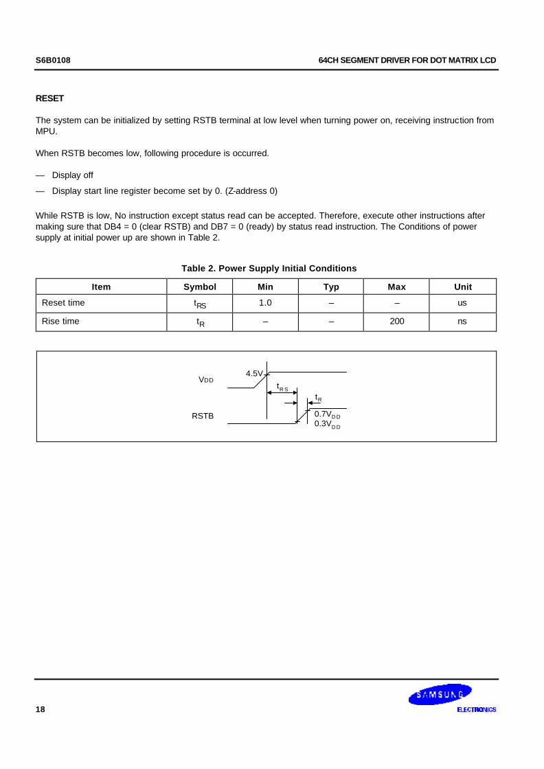
RESET
The system can be initialized by setting RSTB terminal at low level when turning power on, receiving instruction from MPU.
When RSTB becomes low, following procedure is occurred.
— Display off
— Display start line register become set by 0. (Z-address 0)
While RSTB is low, No instruction except status read can be accepted. Therefore, execute other instructions after making sure that DB4 = 0 (clear RSTB) and DB7 = 0 (ready) by status read instruction. The Conditions of power supply at initial power up are shown in Table 2.
Table 2. Power Supply Initial Conditions
Item Symbol Min Typ Max Unit
Reset time tRS 1.0 – – us
Rise time tR – – 200 ns
tR
tR S
4.5VVDD
RSTB 0.7VD D0.3VD D
64CH SEGMENT DRIVER FOR DOT MATRIX LCD S6B0108
19
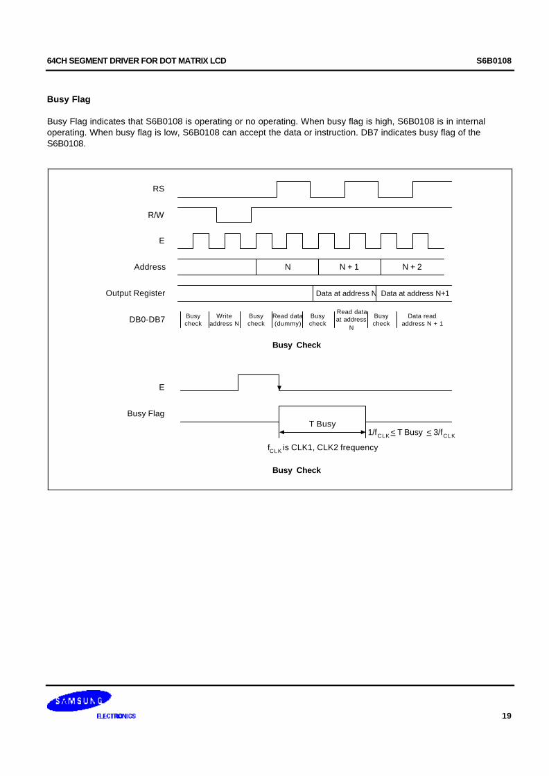
Busy Flag
Busy Flag indicates that S6B0108 is operating or no operating. When busy flag is high, S6B0108 is in internal operating. When busy flag is low, S6B0108 can accept the data or instruction. DB7 indicates busy flag of the S6B0108.
N + 2N + 1N
RS
R/W
E
Address
Data at address N Data at address N+1Output Register
DB0-DB7 Busycheck
Writeaddress N
Busycheck
Read data(dummy)
Busycheck
Read dataat address
N
Busycheck
Data readaddress N + 1
Busy Check
E
Busy FlagT Busy
1/fCLK < T Busy < 3/fCLK
fCLK is CLK1, CLK2 frequency
Busy Check
S6B0108 64CH SEGMENT DRIVER FOR DOT MATRIX LCD
20
Display ON/OFF Flip - Flop
The display on/off flip-flop makes on/off the liquid crystal display. When flip-flop is reset (logical low), selective voltage or non selective voltage appears on segment output terminals. When flip-flop is set (logic high), non selective voltage appears on segment output terminals regardless of display RAM data. The display on/off flip-flop can changes status by instruction. The display data at all segment disappear while RSTB is low. The status of the flip-flop is output to DB5 by status read instruction. The display on/off flip-flop synchronized by CL signal.
X Page Register
X page register designates pages of the internal display data RAM. Count function is not available. An address is set by instruction.
Y Address Counter
Y address counter designates address of the internal display data RAM. An address is set by instruction and is increased by 1 automatically by read or write operations of display data.
Display Data RAM
Display data RAM stores a display data for liquid crystal display. To indicate on state dot matrix of liquid crystal display, write data 1. The other way, off state, writes 0.
Display data RAM address and segment output can be controlled by ADC signal.
— ADC = H → Y-address 0:S1 - Y address 63:S64
— ADC = L → Y-address 0:S64 - Y address 63:S1
ADC terminal connect the VDD or VSS.
Display Start Line Register
The display start line register indicates of display data RAM to display top line of liquid crystal display. Bit data (DB<0:5>) of the display start line set instruction is latched in display start line register. Latched data is transferred to the Z address counter while FRM is high, presetting the Z address counter. It is used for scrolling of the liquid crystal display screen.
64CH SEGMENT DRIVER FOR DOT MATRIX LCD S6B0108
21
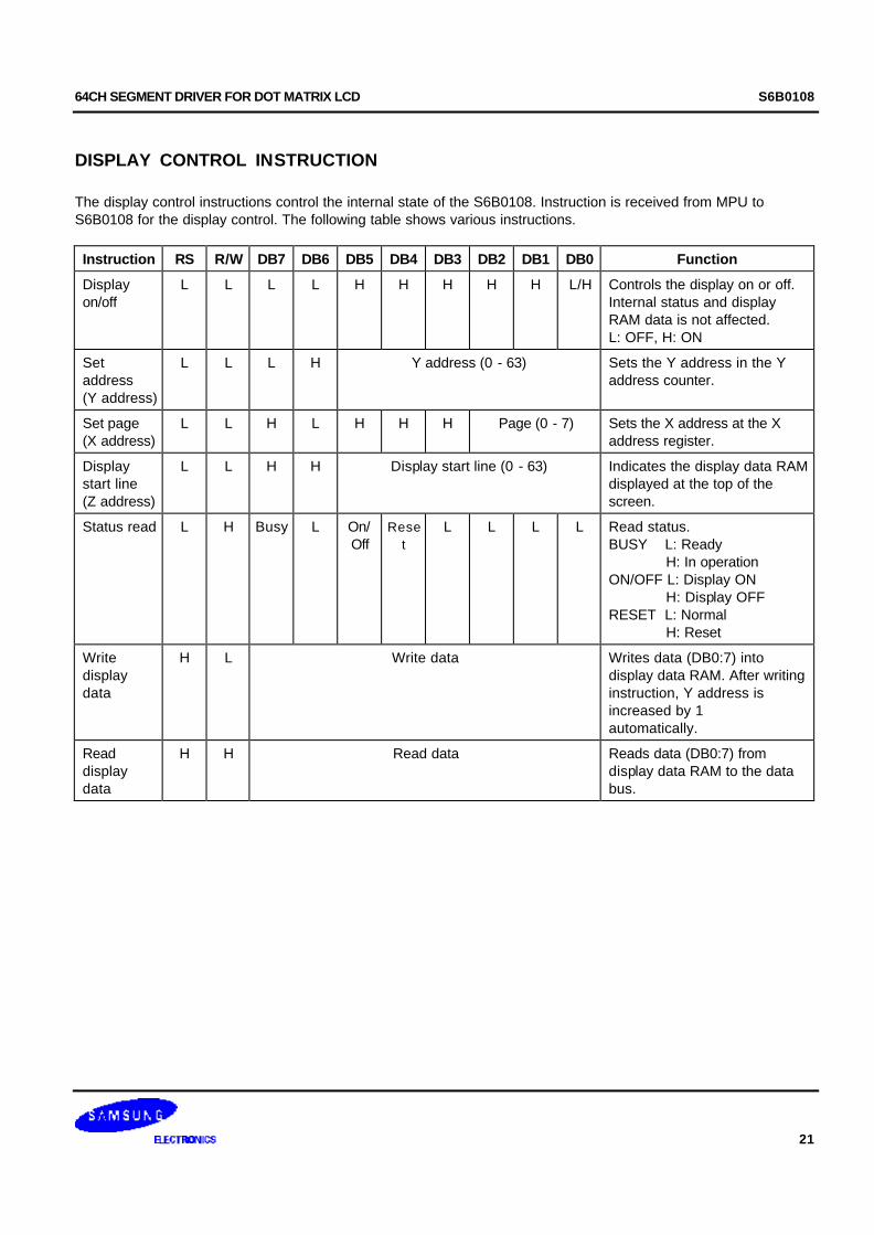
DISPLAY CONTROL INSTRUCTION
The display control instructions control the internal state of the S6B0108. Instruction is received from MPU to S6B0108 for the display control. The following table shows various instructions.
Instruction RS R/W DB7 DB6 DB5 DB4 DB3 DB2 DB1 DB0 Function
Display on/off
L L L L H H H H H L/H Controls the display on or off. Internal status and display RAM data is not affected. L: OFF, H: ON
Set address (Y address)
L L L H Y address (0 - 63) Sets the Y address in the Y address counter.
Set page (X address)
L L H L H H H Page (0 - 7) Sets the X address at the X address register.
Display start line (Z address)
L L H H Display start line (0 - 63) Indicates the display data RAM displayed at the top of the screen.
Status read L H Busy L On/ Off
Reset
L L L L Read status. BUSY L: Ready H: In operation ON/OFF L: Display ON H: Display OFF RESET L: Normal H: Reset
Write display data
H L Write data Writes data (DB0:7) into display data RAM. After writing instruction, Y address is increased by 1 automatically.
Read display data
H H Read data Reads data (DB0:7) from display data RAM to the data bus.
S6B0108 64CH SEGMENT DRIVER FOR DOT MATRIX LCD
22
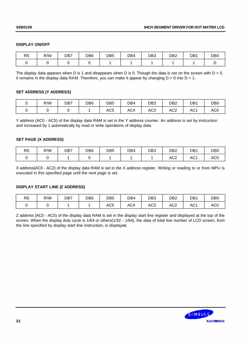
DISPLAY ON/OFF
RS R/W DB7 DB6 DB5 DB4 DB3 DB2 DB1 DB0
0 0 0 0 1 1 1 1 1 D
The display data appears when D is 1 and disappears when D is 0. Though the data is not on the screen with D = 0, it remains in the display data RAM. Therefore, you can make it appear by changing D = 0 into D = 1.
SET ADDRESS (Y ADDRESS)
S R/W DB7 DB6 DB5 DB4 DB3 DB2 DB1 DB0
0 0 0 1 AC5 AC4 AC3 AC2 AC1 AC0
Y address (AC0 - AC5) of the display data RAM is set in the Y address counter. An address is set by instruction and increased by 1 automatically by read or write operations of display data.
SET PAGE (X ADDRESS)
RS R/W DB7 DB6 DB5 DB4 DB3 DB2 DB1 DB0
0 0 1 0 1 1 1 AC2 AC1 AC0
X address(AC0 - AC2) of the display data RAM is set in the X address register. Writing or reading to or from MPU is executed in this specified page until the next page is set.
DISPLAY START LINE (Z ADDRESS)
RS R/W DB7 DB6 DB5 DB4 DB3 DB2 DB1 DB0
0 0 1 1 AC5 AC4 AC3 AC2 AC1 AC0
Z address (AC0 - AC5) of the display data RAM is set in the display start line register and displayed at the top of the screen. When the display duty cycle is 1/64 or others(1/32 - 1/64), the data of total line number of LCD screen, from the line specified by display start line instruction, is displayed.
64CH SEGMENT DRIVER FOR DOT MATRIX LCD S6B0108
23
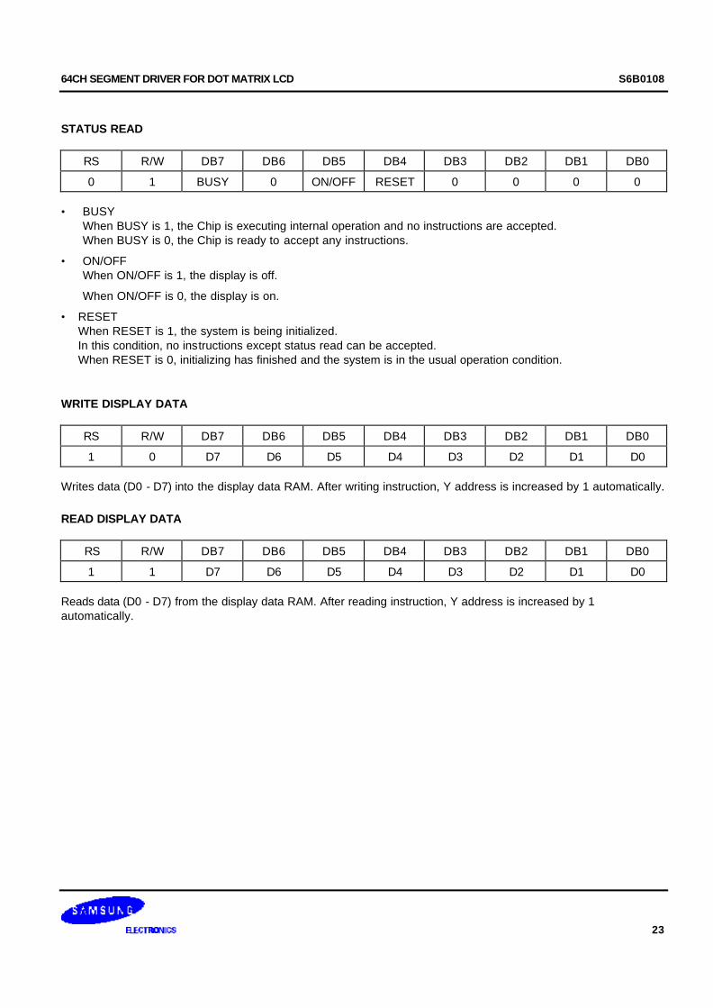
STATUS READ
RS R/W DB7 DB6 DB5 DB4 DB3 DB2 DB1 DB0
0 1 BUSY 0 ON/OFF RESET 0 0 0 0
• BUSY When BUSY is 1, the Chip is executing internal operation and no instructions are accepted. When BUSY is 0, the Chip is ready to accept any instructions.
• ON/OFF When ON/OFF is 1, the display is off.
When ON/OFF is 0, the display is on.
• RESET When RESET is 1, the system is being initialized. In this condition, no instructions except status read can be accepted. When RESET is 0, initializing has finished and the system is in the usual operation condition.
WRITE DISPLAY DATA
RS R/W DB7 DB6 DB5 DB4 DB3 DB2 DB1 DB0
1 0 D7 D6 D5 D4 D3 D2 D1 D0
Writes data (D0 - D7) into the display data RAM. After writing instruction, Y address is increased by 1 automatically.
READ DISPLAY DATA
RS R/W DB7 DB6 DB5 DB4 DB3 DB2 DB1 DB0
1 1 D7 D6 D5 D4 D3 D2 D1 D0
Reads data (D0 - D7) from the display data RAM. After reading instruction, Y address is increased by 1 automatically.
S6B0108 64CH SEGMENT DRIVER FOR DOT MATRIX LCD
24
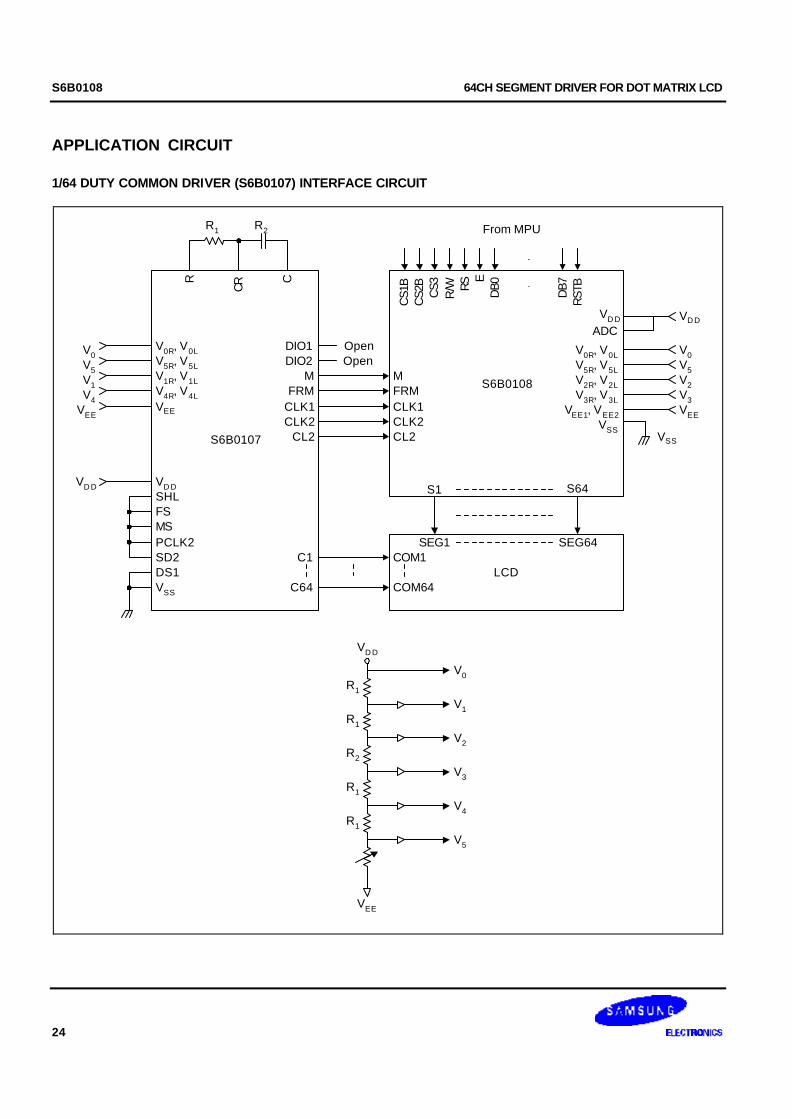
APPLICATION CIRCUIT
1/64 DUTY COMMON DRIVER (S6B0107) INTERFACE CIRCUIT
DIO1DIO2
MFRM
CLK1CLK2
CL2
C1
C64
R
CR
C
RST
BD
B7-
DB0
ERS
R/WCS3
CS2
BC
S1B
VD D
ADCOpenOpen
S1 S64
SEG1 SEG64
LCDCOM1
COM64
From MPU
V0R, V0LV5R, V5LV2R, V2LV3R, V3L
VEE1, VEE2VSS
VD D
V0V5V2V3
VSS
MFRMCLK1CLK2CL2
S6B0108
S6B0107
V0R, V0LV5R, V5LV1R, V1LV4R, V4LVEE
V0V5V1V4
VEE
VSS
DS1SD2PCLK2MSFSSHLVD DVD D
VD D
R1
R1
R2
R1
R1
VEE
V5
V4
V3
V2
V1
V0
-
VEE
R1 R2
64CH SEGMENT DRIVER FOR DOT MATRIX LCD S6B0108
25
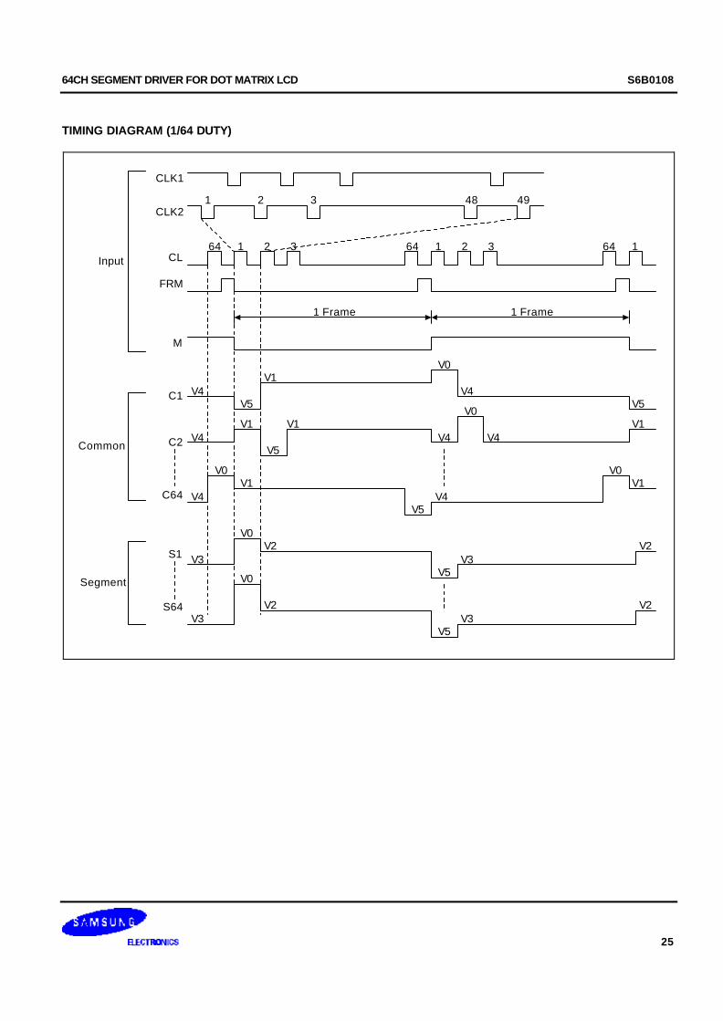
TIMING DIAGRAM (1/64 DUTY)
CLK1
1 2 3 48 49
64 1 2 3 64 1 2 3 64 1
1 Frame 1 Frame
V4V5
V1
V4V1
V5
V1
V0
V4
V4
V0
V4
V5
V1
V4
V0V1
V5V4
V0V1
V2
V2
V5V3
V5V3
V3
V0V2
V0
V2V3
CLK2
CL
FRM
M
C1
C2
C64
S1
S64
Input
Common
Segment
S6B0108 64CH SEGMENT DRIVER FOR DOT MATRIX LCD
26
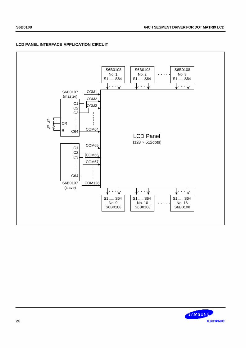
LCD PANEL INTERFACE APPLICATION CIRCUIT
LCD Panel(128 × 512dots)
S6B0108No. 1
S1 ..... S64
S6B0108No. 2
S1 ..... S64
S6B0108No. 8
S1 ..... S64.....
C1C2C3
C64
CR
R
COM1
COM2
COM3
COM64
S6B0107(master)
C1C2C3
C64
S6B0107(slave)
COM65
COM66
COM67
COM128
..... ..... .....
S1 ..... S64No. 9
S6B0108
S1 ..... S64No. 10
S6B0108
S1 ..... S64No. 16
S6B0108.....
..... ..... .....
Cf
Rf
Related Documents