ST Sitronix ST7637 65K 132x132 Color Dot Matrix LCD Controller/Driver Ver 1.6 1/210 2009/03 1. INTRODUCTION The ST7637 is a driver & controller LSI for 65K color graphic dot-matrix liquid crystal display systems. It generates 396 Segment and 132 Common driver circuits. This chip is connected directly to a microprocessor, accepts Serial Peripheral Interface (SPI) or 8-bit/16-bit parallel display data and stores in an on-chip display data RAM. It performs display data RAM read/write operation with no external operating clock to minimize power consumption. In addition, because it contains power supply circuits necessary to drive liquid crystal, it is possible to make a display system with the fewest components. 2. FEATURES Driver Output Circuits ♦ 396 segment outputs / 132 common outputs Applicable Duty Ratios ♦ Various partial display ♦ Partial window moving & data scrolling Gray-Scale Display ♦ 4FRC & 31 PWM function circuit to display 64 gray-scale display ♦ Support 8 color mode (Idle mode) On-chip Display Data RAM ♦ Capacity: 132 x 132 x 16 =278,784 bits Color support by Interface ♦ 256 colors (RGB)=(332) mode ♦ 4k colors (RGB)=(444) mode ♦ 65K colors (RGB)=(565) mode ♦ Truncated 262K colors (RGB)=(666) mode ♦ Truncated 16M colors (RGB)=(888) mode Microprocessor Interface ♦ 8/16-bit parallel bi-directional interface with 6800-series or 8080-series ♦ 4-line serial interface ♦ 3-line (9-bits) serial interface On-chip Low Power Analog Circuit ♦ On-chip oscillator circuit ♦ Voltage converter (x2~x8) with internal capacitors. ♦ Extremely Few Outsider Components. (3 Capacitors) ♦ On-chip Voltage Regulator ♦ On-chip electronic contrast control function ♦ Voltage follower (LCD bias: 1/5~1/12) Operating Voltage Range ♦ Supply Digital Voltage (VDD, VDD1): 1.65 to 3.0V ♦ Supply Analog Voltage (VDD2~VDD5): 2.4 to 3.3V ♦ LCD driving voltage (VOP = V0 - VSS): Max: 18V LCD Driving Voltage (OTP) ♦ Contrast Adjustment Value is stored in the Built-In OTP-ROM for better display quality. LCD Driving setting suggestion ♦ VOP = 14V, BIAS=1/9. (VDD=2.8V) ♦ VOP=15.5V,BIAS=1/10. (VDD=2.8V) Package Type ♦ Application for COG ST7637 6800, 8080, 4-Line, 3-Line interface Sitronix Technology Corp. reserves the right to change the contents in this document without prior notice.

Welcome message from author
This document is posted to help you gain knowledge. Please leave a comment to let me know what you think about it! Share it to your friends and learn new things together.
Transcript

STSitronix ST7637 65K 132x132 Color Dot Matrix LCD Controller/Driver
Ver 1.6 1/210 2009/03
1. INTRODUCTION The ST7637 is a driver & controller LSI for 65K color graphic dot-matrix liquid crystal display systems. It generates 396
Segment and 132 Common driver circuits. This chip is connected directly to a microprocessor, accepts Serial Peripheral
Interface (SPI) or 8-bit/16-bit parallel display data and stores in an on-chip display data RAM. It performs display data RAM
read/write operation with no external operating clock to minimize power consumption. In addition, because it contains
power supply circuits necessary to drive liquid crystal, it is possible to make a display system with the fewest components.
2. FEATURES Driver Output Circuits
♦ 396 segment outputs / 132 common outputs
Applicable Duty Ratios
♦ Various partial display
♦ Partial window moving & data scrolling
Gray-Scale Display
♦ 4FRC & 31 PWM function circuit to display 64
gray-scale display
♦ Support 8 color mode (Idle mode)
On-chip Display Data RAM
♦ Capacity: 132 x 132 x 16 =278,784 bits
Color support by Interface
♦ 256 colors (RGB)=(332) mode
♦ 4k colors (RGB)=(444) mode
♦ 65K colors (RGB)=(565) mode
♦ Truncated 262K colors (RGB)=(666) mode
♦ Truncated 16M colors (RGB)=(888) mode
Microprocessor Interface
♦ 8/16-bit parallel bi-directional interface with 6800-series
or 8080-series
♦ 4-line serial interface
♦ 3-line (9-bits) serial interface
On-chip Low Power Analog Circuit
♦ On-chip oscillator circuit
♦ Voltage converter (x2~x8) with internal capacitors.
♦ Extremely Few Outsider Components. (3 Capacitors)
♦ On-chip Voltage Regulator
♦ On-chip electronic contrast control function
♦ Voltage follower (LCD bias: 1/5~1/12)
Operating Voltage Range
♦ Supply Digital Voltage (VDD, VDD1): 1.65 to 3.0V
♦ Supply Analog Voltage (VDD2~VDD5): 2.4 to 3.3V
♦ LCD driving voltage (VOP = V0 - VSS): Max: 18V
LCD Driving Voltage (OTP)
♦ Contrast Adjustment Value is stored in the Built-In
OTP-ROM for better display quality.
LCD Driving setting suggestion
♦ VOP = 14V, BIAS=1/9. (VDD=2.8V)
♦ VOP=15.5V,BIAS=1/10. (VDD=2.8V)
Package Type
♦ Application for COG
ST7637 6800, 8080, 4-Line, 3-Line interface
Sitronix Technology Corp. reserves the right to change the contents in this document without prior notice.
This controller datasheet was downloaded from http://www.crystalfontz.com/controllers/Crystalfontz
ST7637
Ver 1.6 2/210 2009/03
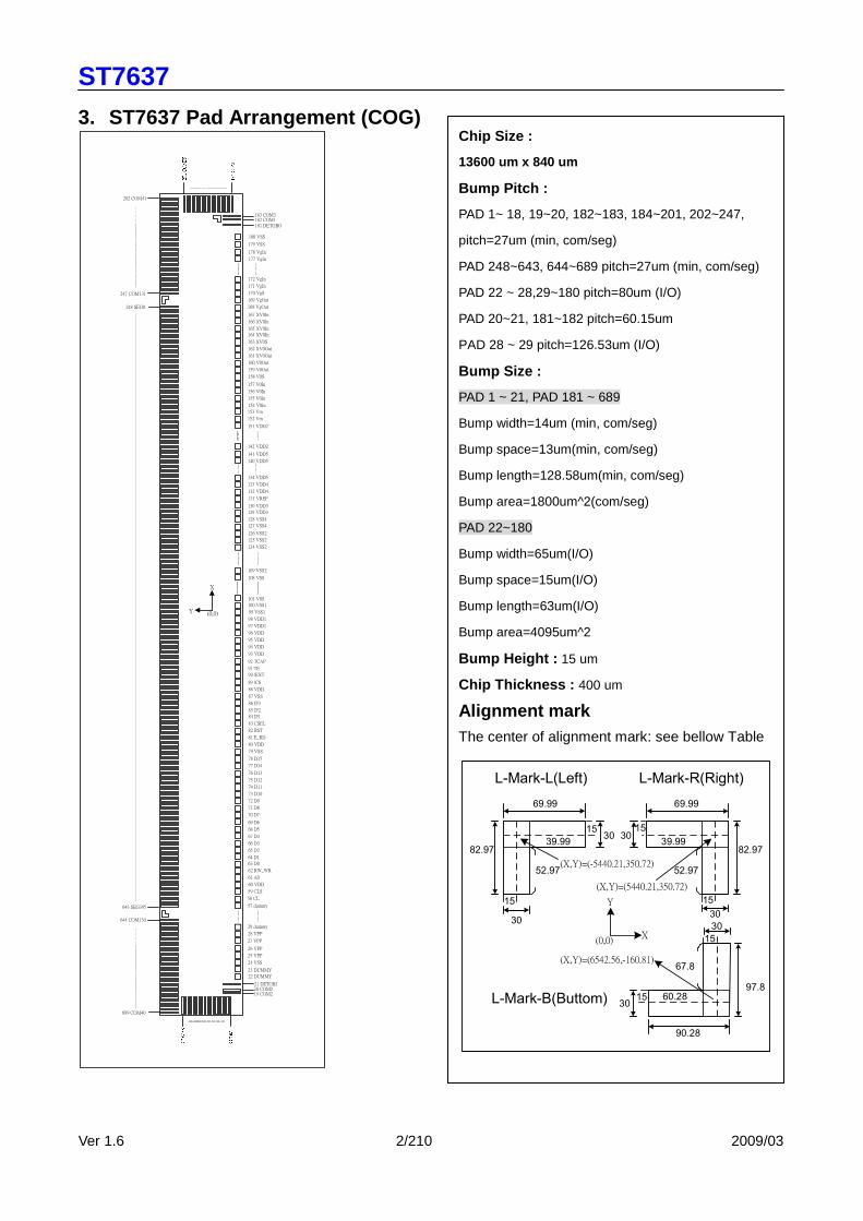
3. ST7637 Pad Arrangement (COG)
Y
X
(0,0)
22 DUMMY
23 DUMMY
24 VSS
25 VPP
26 VPP
29 dummy
202 COM41
247 COM131
59 CLS
60 VDD
61 A0
62 RW_WR
63 D0
64 D1
65 D2
66 D3
67 D4
68 D5
69 D6
70 D7
71 D8
72 D9
73 D10
74 D11
75 D12
76 D13
79 VSS
80 VDD
81 E_RD
82 RST
83 CSEL
84 IF1
85 IF2
86 IF3
87 VSS
88 VDD
89 /CS
90 /EXT
91 TE
92 TCAP
93 VDD
94 VDD
95 VDD
96 VDD
97 VDD1
98 VDD1
99 VSS1
100 VSS1
101 VSS
108 VSS
109 VSS2
77 D14
78 D15
28 VPP
58 CL
57 dummy
153 Vm
134 VDD5
133 VDD4
132 VDD4
130 VDD3
129 VDD3
128 VSS4
127 VSS4
126 VSS2
125 VSS2
179 VSS
178 VgIn
177 VgIn
172 VgIn
171 VgIn
170 VgS
169 VgOut
168 VgOut
167 XV0In
166 XV0In
165 XV0In
164 XV0In
163 XV0S
162 XV0Out
161 XV0Out
160 V0Out
159 V0Out
158 V0S
157 V0In
156 V0In
155 V0In
154 V0In
152 Vm
151 VDD2
142 VDD2
141 VDD5
140 VDD5
180 VSS
181 DETGBO
183 COM3
19 COM220 COM021 DETGBI
27 VPP
124 VSS2
131 VREF
182 COM1
248 SEG0
689 COM40
644 COM130
643 SEG395
Chip Size :
13600 um x 840 um
Bump Pitch :
PAD 1~ 18, 19~20, 182~183, 184~201, 202~247,
pitch=27um (min, com/seg)
PAD 248~643, 644~689 pitch=27um (min, com/seg)
PAD 22 ~ 28,29~180 pitch=80um (I/O)
PAD 20~21, 181~182 pitch=60.15um
PAD 28 ~ 29 pitch=126.53um (I/O)
Bump Size :
PAD 1 ~ 21, PAD 181 ~ 689
Bump width=14um (min, com/seg)
Bump space=13um(min, com/seg)
Bump length=128.58um(min, com/seg)
Bump area=1800um^2(com/seg)
PAD 22~180
Bump width=65um(I/O)
Bump space=15um(I/O)
Bump length=63um(I/O)
Bump area=4095um^2
Bump Height : 15 um
Chip Thickness : 400 um
Alignment mark The center of alignment mark: see bellow Table
L-Mark-R(Right)L-Mark-L(Left)
69.99
82.97
52.97
39.9930
30
30
69.99
82.97
52.97
39.99
30
30
90.28
97.8
67.8
60.28
30
L-Mark-B(Buttom)
15
15
15
15
15
(X,Y)=(-5440.21,350.72)
(X,Y)=(5440.21,350.72)
(X,Y)=(6542.56,-160.81)
(0,0)X
Y
15

ST7637
Ver 1.6 3/210 2009/03
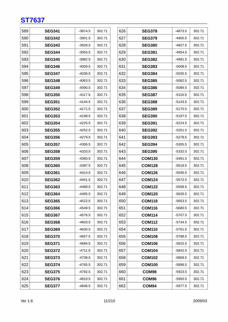
4. Pad Center Coordinates
PAD NAME X Y
1 COM38 -6682.71 146.94
2 COM36 -6682.71 119.94
3 COM34 -6682.71 92.94
4 COM32 -6682.71 65.94
5 COM30 -6682.71 38.94
6 COM28 -6682.71 11.94
7 COM26 -6682.71 -15.06
8 COM24 -6682.71 -42.06
9 COM22 -6682.71 -69.06
10 COM20 -6682.71 -96.06
11 COM18 -6682.71 -123.06
12 COM16 -6682.71 -150.06
13 COM14 -6682.71 -177.06
14 COM12 -6682.71 -204.06
15 COM10 -6682.71 -231.06
16 COM8 -6682.71 -258.06
17 COM6 -6682.71 -285.06
18 COM4 -6682.71 -312.06
19 COM2 -6534.45 -302.71
20 COM0 -6507.45 -302.71
21 DETGBI -6447.3 -302.71
22 DUMMY -6370.88 -329.5
23 DUMMY -6290.88 -329.5
24 VSS -6210.88 -329.5
25 VPP -6130.88 -329.5
26 VPP -6050.88 -329.5
27 VPP -5970.88 -329.5
28 VPP -5890.88 -329.5
29 DUMMY -5764.35 -329.5
30 DUMMY -5684.35 -329.5
31 DUMMY -5604.35 -329.5
32 DUMMY -5524.35 -329.5
33 DUMMY -5444.35 -329.5
34 DUMMY -5364.35 -329.5
35 DUMMY -5284.35 -329.5
36 DUMMY -5204.35 -329.5
37 DUMMY -5124.35 -329.5
38 DUMMY -5044.35 -329.5
39 DUMMY -4964.35 -329.5
40 DUMMY -4884.35 -329.5
41 DUMMY -4804.35 -329.5
42 DUMMY -4724.35 -329.5
43 DUMMY -4644.35 -329.5
44 DUMMY -4564.35 -329.5
45 DUMMY -4484.35 -329.5
46 DUMMY -4404.35 -329.5
47 DUMMY -4324.35 -329.5
48 DUMMY -4244.35 -329.5
49 DUMMY -4164.35 -329.5
50 DUMMY -4084.35 -329.5
51 DUMMY -4004.35 -329.5
52 DUMMY -3924.35 -329.5
53 DUMMY -3844.35 -329.5
54 DUMMY -3764.35 -329.5
55 DUMMY -3684.35 -329.5
56 DUMMY -3604.35 -329.5
57 DUMMY -3524.35 -329.5
58 CL -3444.35 -329.5
59 CLS -3364.35 -329.5
60 VDD -3284.35 -329.5
61 A0 -3204.35 -329.5
62 RW_WR -3124.35 -329.5
63 D0 -3044.35 -329.5
64 D1 -2964.35 -329.5
65 D2 -2884.35 -329.5
66 D3 -2804.35 -329.5
67 D4 -2724.35 -329.5
68 D5 -2644.35 -329.5
69 D6 -2564.35 -329.5
70 D7 -2484.35 -329.5

ST7637
Ver 1.6 4/210 2009/03
71 D8 -2404.35 -329.5
72 D9 -2324.35 -329.5
73 D10 -2244.35 -329.5
74 D11 -2164.35 -329.5
75 D12 -2084.35 -329.5
76 D13 -2004.35 -329.5
77 D14 -1924.35 -329.5
78 D15 -1844.35 -329.5
79 VSS -1764.35 -329.5
80 VDD -1684.35 -329.5
81 E_RD -1604.35 -329.5
82 /RST -1524.35 -329.5
83 CSEL -1444.35 -329.5
84 IF1 -1364.35 -329.5
85 IF2 -1284.35 -329.5
86 IF3 -1204.35 -329.5
87 VSS -1124.35 -329.5
88 VDD -1044.35 -329.5
89 /CS -964.35 -329.5
90 /EXT -884.35 -329.5
91 TE -804.35 -329.5
92 TCAP -724.35 -329.5
93 VDD -644.35 -329.5
94 VDD -564.35 -329.5
95 VDD -484.35 -329.5
96 VDD -404.35 -329.5
97 VDD1 -324.35 -329.5
98 VDD1 -244.35 -329.5
99 VSS1 -164.35 -329.5
100 VSS1 -84.35 -329.5
101 VSS -4.35 -329.5
102 VSS 75.65 -329.5
103 VSS 155.65 -329.5
104 VSS 235.65 -329.5
105 VSS 315.65 -329.5
106 VSS 395.65 -329.5
107 VSS 475.65 -329.5
108 VSS 555.65 -329.5
109 VSS2 635.65 -329.5
110 VSS2 715.65 -329.5
111 VSS2 795.65 -329.5
112 VSS2 875.65 -329.5
113 VSS2 955.65 -329.5
114 VSS2 1035.65 -329.5
115 VSS2 1115.65 -329.5
116 VSS2 1195.65 -329.5
117 VSS2 1275.65 -329.5
118 VSS2 1355.65 -329.5
119 VSS2 1435.65 -329.5
120 VSS2 1515.65 -329.5
121 VSS2 1595.65 -329.5
122 VSS2 1675.65 -329.5
123 VSS2 1755.65 -329.5
124 VSS2 1835.65 -329.5
125 VSS2 1915.65 -329.5
126 VSS2 1995.65 -329.5
127 VSS4 2075.65 -329.5
128 VSS4 2155.65 -329.5
129 VDD3 2235.65 -329.5
130 VDD3 2315.65 -329.5
131 VREFP 2395.65 -329.5
132 VDD4 2475.65 -329.5
133 VDD4 2555.65 -329.5
134 VDD5 2635.65 -329.5
135 VDD5 2715.65 -329.5
136 VDD5 2795.65 -329.5
137 VDD5 2875.65 -329.5
138 VDD5 2955.65 -329.5
139 VDD5 3035.65 -329.5
140 VDD5 3115.65 -329.5
141 VDD5 3195.65 -329.5
142 VDD2 3275.65 -329.5
143 VDD2 3355.65 -329.5
144 VDD2 3435.65 -329.5

ST7637
Ver 1.6 5/210 2009/03
145 VDD2 3515.65 -329.5
146 VDD2 3595.65 -329.5
147 VDD2 3675.65 -329.5
148 VDD2 3755.65 -329.5
149 VDD2 3835.65 -329.5
150 VDD2 3915.65 -329.5
151 VDD2 3995.65 -329.5
152 Vm 4075.65 -329.5
153 Vm 4155.65 -329.5
154 V0in 4235.65 -329.5
155 V0in 4315.65 -329.5
156 V0in 4395.65 -329.5
157 V0in 4475.65 -329.5
158 V0s 4555.65 -329.5
159 V0out 4635.65 -329.5
160 V0out 4715.65 -329.5
161 XV0out 4795.65 -329.5
162 XV0out 4875.65 -329.5
163 XV0s 4955.65 -329.5
164 XV0in 5035.65 -329.5
165 XV0in 5115.65 -329.5
166 XV0in 5195.65 -329.5
167 XV0in 5275.65 -329.5
168 Vgout 5355.65 -329.5
169 Vgout 5435.65 -329.5
170 Vgs 5515.65 -329.5
171 Vgin 5595.65 -329.5
172 Vgin 5675.65 -329.5
173 Vgin 5755.65 -329.5
174 Vgin 5835.65 -329.5
175 Vgin 5915.65 -329.5
176 Vgin 5995.65 -329.5
177 Vgin 6075.65 -329.5
178 Vgin 6155.65 -329.5
179 VSS 6235.65 -329.5
180 VSS 6315.65 -329.5
181 DETGBO 6447.3 -302.71
182 COM1 6507.45 -302.71
183 COM3 6534.45 -302.71
184 COM5 6682.71 -312.06
185 COM7 6682.71 -285.06
186 COM9 6682.71 -258.06
187 COM11 6682.71 -231.06
188 COM13 6682.71 -204.06
189 COM15 6682.71 -177.06
190 COM17 6682.71 -150.06
191 COM19 6682.71 -123.06
192 COM21 6682.71 -96.06
193 COM23 6682.71 -69.06
194 COM25 6682.71 -42.06
195 COM27 6682.71 -15.06
196 COM29 6682.71 11.94
197 COM31 6682.71 38.94
198 COM33 6682.71 65.94
199 COM35 6682.71 92.94
200 COM37 6682.71 119.94
201 COM39 6682.71 146.94
202 COM41 6706.5 302.71
203 COM43 6679.5 302.71
204 COM45 6652.5 302.71
205 COM47 6625.5 302.71
206 COM49 6598.5 302.71
207 COM51 6571.5 302.71
208 COM53 6544.5 302.71
209 COM55 6517.5 302.71
210 COM57 6490.5 302.71
211 COM59 6463.5 302.71
212 COM61 6436.5 302.71
213 COM63 6409.5 302.71
214 COM65 6382.5 302.71
215 COM67 6355.5 302.71
216 COM69 6328.5 302.71
217 COM71 6301.5 302.71
218 COM73 6274.5 302.71

ST7637
Ver 1.6 6/210 2009/03
219 COM75 6247.5 302.71
220 COM77 6220.5 302.71
221 COM79 6193.5 302.71
222 COM81 6166.5 302.71
223 COM83 6139.5 302.71
224 COM85 6112.5 302.71
225 COM87 6085.5 302.71
226 COM89 6058.5 302.71
227 COM91 6031.5 302.71
228 COM93 6004.5 302.71
229 COM95 5977.5 302.71
230 COM97 5950.5 302.71
231 COM99 5923.5 302.71
232 COM101 5896.5 302.71
233 COM103 5869.5 302.71
234 COM105 5842.5 302.71
235 COM107 5815.5 302.71
236 COM109 5788.5 302.71
237 COM111 5761.5 302.71
238 COM113 5734.5 302.71
239 COM115 5707.5 302.71
240 COM117 5680.5 302.71
241 COM119 5653.5 302.71
242 COM121 5626.5 302.71
243 COM123 5599.5 302.71
244 COM125 5572.5 302.71
245 COM127 5545.5 302.71
246 COM129 5518.5 302.71
247 COM131 5491.5 302.71
248 SEG0 5332.5 302.71
249 SEG1 5305.5 302.71
250 SEG2 5278.5 302.71
251 SEG3 5251.5 302.71
252 SEG4 5224.5 302.71
253 SEG5 5197.5 302.71
254 SEG6 5170.5 302.71
255 SEG7 5143.5 302.71
256 SEG8 5116.5 302.71
257 SEG9 5089.5 302.71
258 SEG10 5062.5 302.71
259 SEG11 5035.5 302.71
260 SEG12 5008.5 302.71
261 SEG13 4981.5 302.71
262 SEG14 4954.5 302.71
263 SEG15 4927.5 302.71
264 SEG16 4900.5 302.71
265 SEG17 4873.5 302.71
266 SEG18 4846.5 302.71
267 SEG19 4819.5 302.71
268 SEG20 4792.5 302.71
269 SEG21 4765.5 302.71
270 SEG22 4738.5 302.71
271 SEG23 4711.5 302.71
272 SEG24 4684.5 302.71
273 SEG25 4657.5 302.71
274 SEG26 4630.5 302.71
275 SEG27 4603.5 302.71
276 SEG28 4576.5 302.71
277 SEG29 4549.5 302.71
278 SEG30 4522.5 302.71
279 SEG31 4495.5 302.71
280 SEG32 4468.5 302.71
281 SEG33 4441.5 302.71
282 SEG34 4414.5 302.71
283 SEG35 4387.5 302.71
284 SEG36 4360.5 302.71
285 SEG37 4333.5 302.71
286 SEG38 4306.5 302.71
287 SEG39 4279.5 302.71
288 SEG40 4252.5 302.71
289 SEG41 4225.5 302.71
290 SEG42 4198.5 302.71
291 SEG43 4171.5 302.71
292 SEG44 4144.5 302.71

ST7637
Ver 1.6 7/210 2009/03
293 SEG45 4117.5 302.71
294 SEG46 4090.5 302.71
295 SEG47 4063.5 302.71
296 SEG48 4036.5 302.71
297 SEG49 4009.5 302.71
298 SEG50 3982.5 302.71
299 SEG51 3955.5 302.71
300 SEG52 3928.5 302.71
301 SEG53 3901.5 302.71
302 SEG54 3874.5 302.71
303 SEG55 3847.5 302.71
304 SEG56 3820.5 302.71
305 SEG57 3793.5 302.71
306 SEG58 3766.5 302.71
307 SEG59 3739.5 302.71
308 SEG60 3712.5 302.71
309 SEG61 3685.5 302.71
310 SEG62 3658.5 302.71
311 SEG63 3631.5 302.71
312 SEG64 3604.5 302.71
313 SEG65 3577.5 302.71
314 SEG66 3550.5 302.71
315 SEG67 3523.5 302.71
316 SEG68 3496.5 302.71
317 SEG69 3469.5 302.71
318 SEG70 3442.5 302.71
319 SEG71 3415.5 302.71
320 SEG72 3388.5 302.71
321 SEG73 3361.5 302.71
322 SEG74 3334.5 302.71
323 SEG75 3307.5 302.71
324 SEG76 3280.5 302.71
325 SEG77 3253.5 302.71
326 SEG78 3226.5 302.71
327 SEG79 3199.5 302.71
328 SEG80 3172.5 302.71
329 SEG81 3145.5 302.71
330 SEG82 3118.5 302.71
331 SEG83 3091.5 302.71
332 SEG84 3064.5 302.71
333 SEG85 3037.5 302.71
334 SEG86 3010.5 302.71
335 SEG87 2983.5 302.71
336 SEG88 2956.5 302.71
337 SEG89 2929.5 302.71
338 SEG90 2902.5 302.71
339 SEG91 2875.5 302.71
340 SEG92 2848.5 302.71
341 SEG93 2821.5 302.71
342 SEG94 2794.5 302.71
343 SEG95 2767.5 302.71
344 SEG96 2740.5 302.71
345 SEG97 2713.5 302.71
346 SEG98 2686.5 302.71
347 SEG99 2659.5 302.71
348 SEG100 2632.5 302.71
349 SEG101 2605.5 302.71
350 SEG102 2578.5 302.71
351 SEG103 2551.5 302.71
352 SEG104 2524.5 302.71
353 SEG105 2497.5 302.71
354 SEG106 2470.5 302.71
355 SEG107 2443.5 302.71
356 SEG108 2416.5 302.71
357 SEG109 2389.5 302.71
358 SEG110 2362.5 302.71
359 SEG111 2335.5 302.71
360 SEG112 2308.5 302.71
361 SEG113 2281.5 302.71
362 SEG114 2254.5 302.71
363 SEG115 2227.5 302.71
364 SEG116 2200.5 302.71
365 SEG117 2173.5 302.71
366 SEG118 2146.5 302.71

ST7637
Ver 1.6 8/210 2009/03
367 SEG119 2119.5 302.71
368 SEG120 2092.5 302.71
369 SEG121 2065.5 302.71
370 SEG122 2038.5 302.71
371 SEG123 2011.5 302.71
372 SEG124 1984.5 302.71
373 SEG125 1957.5 302.71
374 SEG126 1930.5 302.71
375 SEG127 1903.5 302.71
376 SEG128 1876.5 302.71
377 SEG129 1849.5 302.71
378 SEG130 1822.5 302.71
379 SEG131 1795.5 302.71
380 SEG132 1768.5 302.71
381 SEG133 1741.5 302.71
382 SEG134 1714.5 302.71
383 SEG135 1687.5 302.71
384 SEG136 1660.5 302.71
385 SEG137 1633.5 302.71
386 SEG138 1606.5 302.71
387 SEG139 1579.5 302.71
388 SEG140 1552.5 302.71
389 SEG141 1525.5 302.71
390 SEG142 1498.5 302.71
391 SEG143 1471.5 302.71
392 SEG144 1444.5 302.71
393 SEG145 1417.5 302.71
394 SEG146 1390.5 302.71
395 SEG147 1363.5 302.71
396 SEG148 1336.5 302.71
397 SEG149 1309.5 302.71
398 SEG150 1282.5 302.71
399 SEG151 1255.5 302.71
400 SEG152 1228.5 302.71
401 SEG153 1201.5 302.71
402 SEG154 1174.5 302.71
403 SEG155 1147.5 302.71
404 SEG156 1120.5 302.71
405 SEG157 1093.5 302.71
406 SEG158 1066.5 302.71
407 SEG159 1039.5 302.71
408 SEG160 1012.5 302.71
409 SEG161 985.5 302.71
410 SEG162 958.5 302.71
411 SEG163 931.5 302.71
412 SEG164 904.5 302.71
413 SEG165 877.5 302.71
414 SEG166 850.5 302.71
415 SEG167 823.5 302.71
416 SEG168 796.5 302.71
417 SEG169 769.5 302.71
418 SEG170 742.5 302.71
419 SEG171 715.5 302.71
420 SEG172 688.5 302.71
421 SEG173 661.5 302.71
422 SEG174 634.5 302.71
423 SEG175 607.5 302.71
424 SEG176 580.5 302.71
425 SEG177 553.5 302.71
426 SEG178 526.5 302.71
427 SEG179 499.5 302.71
428 SEG180 472.5 302.71
429 SEG181 445.5 302.71
430 SEG182 418.5 302.71
431 SEG183 391.5 302.71
432 SEG184 364.5 302.71
433 SEG185 337.5 302.71
434 SEG186 310.5 302.71
435 SEG187 283.5 302.71
436 SEG188 256.5 302.71
437 SEG189 229.5 302.71
438 SEG190 202.5 302.71
439 SEG191 175.5 302.71
440 SEG192 148.5 302.71

ST7637
Ver 1.6 9/210 2009/03
441 SEG193 121.5 302.71
442 SEG194 94.5 302.71
443 SEG195 67.5 302.71
444 SEG196 40.5 302.71
445 SEG197 13.5 302.71
446 SEG198 -13.5 302.71
447 SEG199 -40.5 302.71
448 SEG200 -67.5 302.71
449 SEG201 -94.5 302.71
450 SEG202 -121.5 302.71
451 SEG203 -148.5 302.71
452 SEG204 -175.5 302.71
453 SEG205 -202.5 302.71
454 SEG206 -229.5 302.71
455 SEG207 -256.5 302.71
456 SEG208 -283.5 302.71
457 SEG209 -310.5 302.71
458 SEG210 -337.5 302.71
459 SEG211 -364.5 302.71
460 SEG212 -391.5 302.71
461 SEG213 -418.5 302.71
462 SEG214 -445.5 302.71
463 SEG215 -472.5 302.71
464 SEG216 -499.5 302.71
465 SEG217 -526.5 302.71
466 SEG218 -553.5 302.71
467 SEG219 -580.5 302.71
468 SEG220 -607.5 302.71
469 SEG221 -634.5 302.71
470 SEG222 -661.5 302.71
471 SEG223 -688.5 302.71
472 SEG224 -715.5 302.71
473 SEG225 -742.5 302.71
474 SEG226 -769.5 302.71
475 SEG227 -796.5 302.71
476 SEG228 -823.5 302.71
477 SEG229 -850.5 302.71
478 SEG230 -877.5 302.71
479 SEG231 -904.5 302.71
480 SEG232 -931.5 302.71
481 SEG233 -958.5 302.71
482 SEG234 -985.5 302.71
483 SEG235 -1012.5 302.71
484 SEG236 -1039.5 302.71
485 SEG237 -1066.5 302.71
486 SEG238 -1093.5 302.71
487 SEG239 -1120.5 302.71
488 SEG240 -1147.5 302.71
489 SEG241 -1174.5 302.71
490 SEG242 -1201.5 302.71
491 SEG243 -1228.5 302.71
492 SEG244 -1255.5 302.71
493 SEG245 -1282.5 302.71
494 SEG246 -1309.5 302.71
495 SEG247 -1336.5 302.71
496 SEG248 -1363.5 302.71
497 SEG249 -1390.5 302.71
498 SEG250 -1417.5 302.71
499 SEG251 -1444.5 302.71
500 SEG252 -1471.5 302.71
501 SEG253 -1498.5 302.71
502 SEG254 -1525.5 302.71
503 SEG255 -1552.5 302.71
504 SEG256 -1579.5 302.71
505 SEG257 -1606.5 302.71
506 SEG258 -1633.5 302.71
507 SEG259 -1660.5 302.71
508 SEG260 -1687.5 302.71
509 SEG261 -1714.5 302.71
510 SEG262 -1741.5 302.71
511 SEG263 -1768.5 302.71
512 SEG264 -1795.5 302.71
513 SEG265 -1822.5 302.71
514 SEG266 -1849.5 302.71

ST7637
Ver 1.6 10/210 2009/03
515 SEG267 -1876.5 302.71
516 SEG268 -1903.5 302.71
517 SEG269 -1930.5 302.71
518 SEG270 -1957.5 302.71
519 SEG271 -1984.5 302.71
520 SEG272 -2011.5 302.71
521 SEG273 -2038.5 302.71
522 SEG274 -2065.5 302.71
523 SEG275 -2092.5 302.71
524 SEG276 -2119.5 302.71
525 SEG277 -2146.5 302.71
526 SEG278 -2173.5 302.71
527 SEG279 -2200.5 302.71
528 SEG280 -2227.5 302.71
529 SEG281 -2254.5 302.71
530 SEG282 -2281.5 302.71
531 SEG283 -2308.5 302.71
532 SEG284 -2335.5 302.71
533 SEG285 -2362.5 302.71
534 SEG286 -2389.5 302.71
535 SEG287 -2416.5 302.71
536 SEG288 -2443.5 302.71
537 SEG289 -2470.5 302.71
538 SEG290 -2497.5 302.71
539 SEG291 -2524.5 302.71
540 SEG292 -2551.5 302.71
541 SEG293 -2578.5 302.71
542 SEG294 -2605.5 302.71
543 SEG295 -2632.5 302.71
544 SEG296 -2659.5 302.71
545 SEG297 -2686.5 302.71
546 SEG298 -2713.5 302.71
547 SEG299 -2740.5 302.71
548 SEG300 -2767.5 302.71
549 SEG301 -2794.5 302.71
550 SEG302 -2821.5 302.71
551 SEG303 -2848.5 302.71
552 SEG304 -2875.5 302.71
553 SEG305 -2902.5 302.71
554 SEG306 -2929.5 302.71
555 SEG307 -2956.5 302.71
556 SEG308 -2983.5 302.71
557 SEG309 -3010.5 302.71
558 SEG310 -3037.5 302.71
559 SEG311 -3064.5 302.71
560 SEG312 -3091.5 302.71
561 SEG313 -3118.5 302.71
562 SEG314 -3145.5 302.71
563 SEG315 -3172.5 302.71
564 SEG316 -3199.5 302.71
565 SEG317 -3226.5 302.71
566 SEG318 -3253.5 302.71
567 SEG319 -3280.5 302.71
568 SEG320 -3307.5 302.71
569 SEG321 -3334.5 302.71
570 SEG322 -3361.5 302.71
571 SEG323 -3388.5 302.71
572 SEG324 -3415.5 302.71
573 SEG325 -3442.5 302.71
574 SEG326 -3469.5 302.71
575 SEG327 -3496.5 302.71
576 SEG328 -3523.5 302.71
577 SEG329 -3550.5 302.71
578 SEG330 -3577.5 302.71
579 SEG331 -3604.5 302.71
580 SEG332 -3631.5 302.71
581 SEG333 -3658.5 302.71
582 SEG334 -3685.5 302.71
583 SEG335 -3712.5 302.71
584 SEG336 -3739.5 302.71
585 SEG337 -3766.5 302.71
586 SEG338 -3793.5 302.71
587 SEG339 -3820.5 302.71
588 SEG340 -3847.5 302.71
ST7637
Ver 1.6 11/210 2009/03
589 SEG341 -3874.5 302.71
590 SEG342 -3901.5 302.71
591 SEG343 -3928.5 302.71
592 SEG344 -3955.5 302.71
593 SEG345 -3982.5 302.71
594 SEG346 -4009.5 302.71
595 SEG347 -4036.5 302.71
596 SEG348 -4063.5 302.71
597 SEG349 -4090.5 302.71
598 SEG350 -4117.5 302.71
599 SEG351 -4144.5 302.71
600 SEG352 -4171.5 302.71
601 SEG353 -4198.5 302.71
602 SEG354 -4225.5 302.71
603 SEG355 -4252.5 302.71
604 SEG356 -4279.5 302.71
605 SEG357 -4306.5 302.71
606 SEG358 -4333.5 302.71
607 SEG359 -4360.5 302.71
608 SEG360 -4387.5 302.71
609 SEG361 -4414.5 302.71
610 SEG362 -4441.5 302.71
611 SEG363 -4468.5 302.71
612 SEG364 -4495.5 302.71
613 SEG365 -4522.5 302.71
614 SEG366 -4549.5 302.71
615 SEG367 -4576.5 302.71
616 SEG368 -4603.5 302.71
617 SEG369 -4630.5 302.71
618 SEG370 -4657.5 302.71
619 SEG371 -4684.5 302.71
620 SEG372 -4711.5 302.71
621 SEG373 -4738.5 302.71
622 SEG374 -4765.5 302.71
623 SEG375 -4792.5 302.71
624 SEG376 -4819.5 302.71
625 SEG377 -4846.5 302.71
626 SEG378 -4873.5 302.71
627 SEG379 -4900.5 302.71
628 SEG380 -4927.5 302.71
629 SEG381 -4954.5 302.71
630 SEG382 -4981.5 302.71
631 SEG383 -5008.5 302.71
632 SEG384 -5035.5 302.71
633 SEG385 -5062.5 302.71
634 SEG386 -5089.5 302.71
635 SEG387 -5116.5 302.71
636 SEG388 -5143.5 302.71
637 SEG389 -5170.5 302.71
638 SEG390 -5197.5 302.71
639 SEG391 -5224.5 302.71
640 SEG392 -5251.5 302.71
641 SEG393 -5278.5 302.71
642 SEG394 -5305.5 302.71
643 SEG395 -5332.5 302.71
644 COM130 -5491.5 302.71
645 COM128 -5518.5 302.71
646 COM126 -5545.5 302.71
647 COM124 -5572.5 302.71
648 COM122 -5599.5 302.71
649 COM120 -5626.5 302.71
650 COM118 -5653.5 302.71
651 COM116 -5680.5 302.71
652 COM114 -5707.5 302.71
653 COM112 -5734.5 302.71
654 COM110 -5761.5 302.71
655 COM108 -5788.5 302.71
656 COM106 -5815.5 302.71
657 COM104 -5842.5 302.71
658 COM102 -5869.5 302.71
659 COM100 -5896.5 302.71
660 COM98 -5923.5 302.71
661 COM96 -5950.5 302.71
662 COM94 -5977.5 302.71
ST7637
Ver 1.6 12/210 2009/03
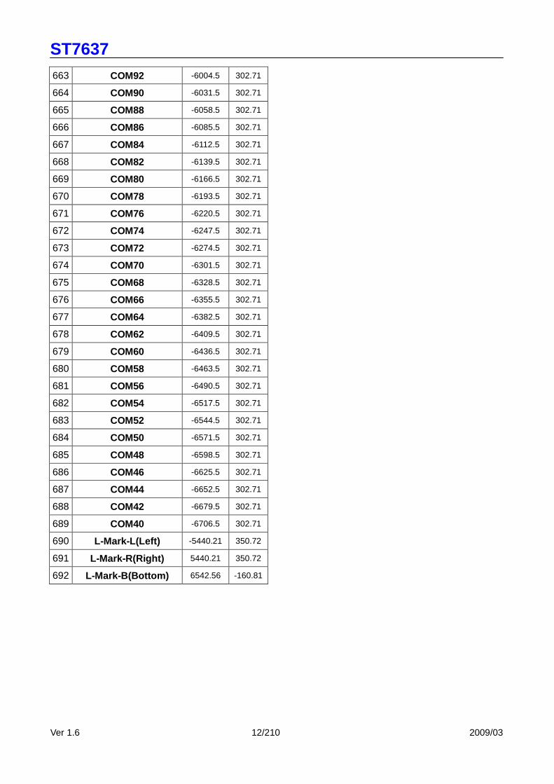
663 COM92 -6004.5 302.71
664 COM90 -6031.5 302.71
665 COM88 -6058.5 302.71
666 COM86 -6085.5 302.71
667 COM84 -6112.5 302.71
668 COM82 -6139.5 302.71
669 COM80 -6166.5 302.71
670 COM78 -6193.5 302.71
671 COM76 -6220.5 302.71
672 COM74 -6247.5 302.71
673 COM72 -6274.5 302.71
674 COM70 -6301.5 302.71
675 COM68 -6328.5 302.71
676 COM66 -6355.5 302.71
677 COM64 -6382.5 302.71
678 COM62 -6409.5 302.71
679 COM60 -6436.5 302.71
680 COM58 -6463.5 302.71
681 COM56 -6490.5 302.71
682 COM54 -6517.5 302.71
683 COM52 -6544.5 302.71
684 COM50 -6571.5 302.71
685 COM48 -6598.5 302.71
686 COM46 -6625.5 302.71
687 COM44 -6652.5 302.71
688 COM42 -6679.5 302.71
689 COM40 -6706.5 302.71
690 L-Mark-L(Left) -5440.21 350.72
691 L-Mark-R(Right) 5440.21 350.72
692 L-Mark-B(Bottom) 6542.56 -160.81
ST7637
Ver 1.6 13/210 2009/03
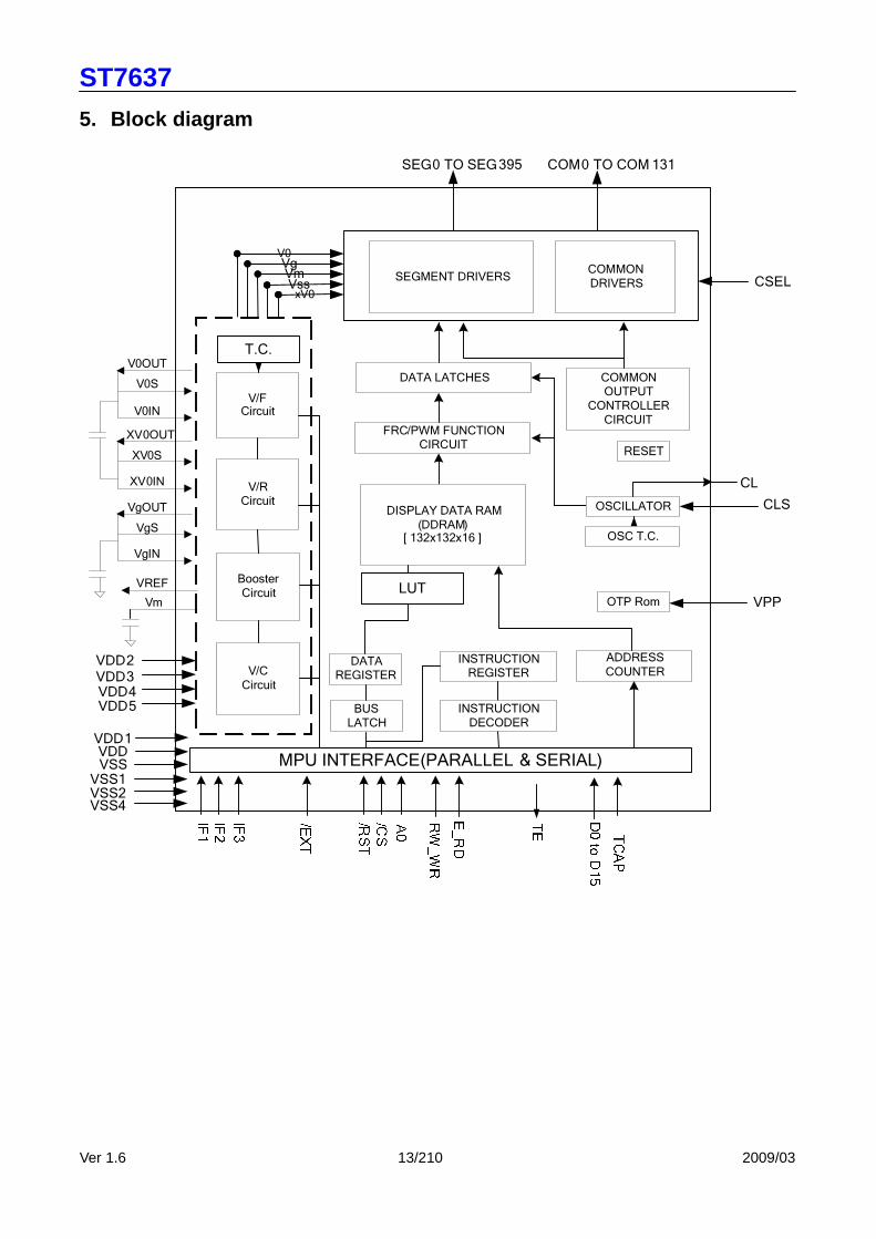
5. Block diagram
V/FCircuit
V/RCircuit
SEGMENT DRIVERS
DATA LATCHES
COMMONDRIVERS
COMMONOUTPUT
CONTROLLERCIRCUIT
RESET
MPU INTERFACE(PARALLEL & SERIAL)VDD
COM0 TO COM131SEG0 TO SEG395
CLS
FRC/PWM FUNCTIONCIRCUIT
DISPLAY DATA RAM(DDRAM)
[ 132x132x16 ]
BUSLATCH
DATAREGISTER
INSTRUCTIONREGISTER
OSCILLATOR
INSTRUCTIONDECODER
BoosterCircuit
V0VgVmVssxV0
VDD1
VDD3
CSEL
VDD2
VDD5VDD4
CL
OTP Rom
VgOUT
VgS
VgIN
V0OUT
V0S
V0IN
XV0OUT
XV0S
XV0IN
VREF
Vm
V/CCircuit
VPP
OSC T.C.
T.C.
LUT
ADDRESSCOUNTER
VSSVSS1VSS2VSS4

ST7637
Ver 1.6 14/210 2009/03
6. PIN DESCRIPTION 6.1 Power Supply Name I/O Description
VDD Supply Power supply for logic circuit.
VDD1 Supply Power supply for OSC circuit.
VDD2 Supply Power supply for Booster circuit.
VDD3 Supply Power supply for LCD.
VDD4 Supply Power supply for LCD.
VDD5 Supply Power supply for LCD.
VSS Supply Ground for logic circuit. Ground system should be connected together.
VSS1 Supply Ground for OSC circuit. Ground system should be connected together.
VSS2 Supply Ground for Booster circuit. Ground system should be connected together.
VSS4 Supply Ground for LCD. Ground system should be connected together.
6.2 LCD Power Supply Pins
Name I/O Description
V0OUT
V0IN
V0S
I/O
Positive LCD driver supply voltages.
V0OUT is the output voltage of V0 generated by ST7637.
V0IN is the input pin of power supply to generate V0 voltage for LCD.
V0S is the input pin of power supply to sense the V0 voltage.
V0OUT 、V0IN & V0S should be connected together by FPC.
XV0OUT
XV0IN
XV0S
I/O
Negative LCD driver supply voltages.
XV0OUT is the output voltage of XV0 generated by ST7637.
XV0IN is the input pin of power supply to generate XV0 voltage for LCD.
XV0S is the input pin of power supply to sense the XV0 voltage.
XV0OUT 、XV0IN & XV0S should be connected together by FPC.
VgOUT
VgIN
VgS
Vm
I/O
Bias LCD driver supply voltages.
VgOUT is the output voltage of Vg generated by ST7637.
VgIN is the input pin of power supply to generate Vg voltage for LCD.
VgS is the input pin of power supply to sense the Vg voltage.
VgOUT 、VgIN & VgS should be connected together by FPC.
Vm is the I/O pin of LCD bias supply voltage
Voltages should have the following relationship;
V0 > Vg > Vm > VSS > XV0.
VDDA-0.7V>Vm>0.7V.
VddA <3V:2 x VDDA Vg≧ ≧3V ; VddA ≧3V:2 x VDDA Vg≧ >1.8V
When the internal power circuit is active, these voltages are generated as following table according
to the state of LCD bias.
NOTE: N = 5 to 12
LCD bias Vg Vm
1/N bias (2/N) x V0 (1/N) x V0

ST7637
Ver 1.6 15/210 2009/03
6.3 System Control Name I/O Description
CLS I Reserve for testing only.
Please fix this pin to VDDI.
CL I/O Reserve for testing only. Leave this pin open.
CSEL I This pin should connect to VDDI.
TCAP I/O Test pin. Left it opens.
VREF O Reference voltage output for monitor only. Left it opened.
VPP I When writing OTP, it needs external power supply voltage 7.5V~7.75V input to write successfully.
6.4 Microprocessor Interface Name I/O Description
/RST I Reset input pin
When /RST is “L”, initialization is executed.
IF[3:1] I
Parallel / Serial data input select input
IF3 IF2 IF1 MPU interface type
H H H 80 series 16-bit parallel
H H L 80 series 8-bit parallel
H L H 68 series 16-bit parallel
H L L 68 series 8-bit parallel
L H H 8-bit serial (4 line)
L H L 9-bit serial (3 line)
Note:
Refer to Table 7.2-1 for detail interface connectio ns.
/CS I
Chip select input pins
Data / Instruction I/O is enabled only when /CS is "L". When chip select is non-active, D0 to D15
become high impedance.
A0 I
Register select input pin
In parallel interface:
A0 = "H": D0 to D15 or SI are display data
A0 = "L": D0 to D15 or SI are control Command
In 3-line/4-line interface:
This pad will be used for SCL function.
ST7637
Ver 1.6 16/210 2009/03
RW_WR I
RW_WR pin is only used in parallel interface.
MPU type RW_WR Description
6800-series RW
Read / Write control input pin
Write status: RW = “L”.
Read status: RW = “H”.
8080-series /WR
Write enable clock input pin
The data on D0 to D15 are latched at the rising
edge of the /WR signal.
When in the serial interface, connect it to VDDI.
E_RD I
E_RD pin is only used in parallel interface.
MPU Type E_RD Description
6800-series E
Enable clock pin:
Write status: The data on D0 to D15 are latched at
the falling edge of the E signal.
Read status: The data on D0 to D15 are latched at
the rising edge of the E signal.
8080-series /RD
Read enable clock input pin
The data on D0 to D15 are latched at the falling
edge of the /WR signal.
When in the serial interface, connect it to VDDI.
D15 to D0 I/O
They connect to the standard 8-bit or 16 bit MPU bus via the 8/16 –bit bi-directional bus.
When the following interface is selected and the /CS pin is high, the following pins become high
impedance.
1. In 8-bit parallel: D15-D8 pins are in the state of high impedance should connect to VDDI.
2. In 3-line/4-line interface D0 pad will be used for SI function
3. In 4-line interface D1 pad will be used for A0 function
4. In Serial interface: unused pins are in the state of high impedance should connect to VDDI.
SI I
SI is used to input serial data when the serial interface is selected.(3 line and 4 line)
It is used by “D0” pad, See Table 7.2-1.
SCL I
SCL is used to input serial clock when the serial interface is selected.
The data is converted in the rising edge. (3 line and 4 line)
It is used by “A0” pad , See Table 7.2-1.
TE O Tearing effect output.

ST7637
Ver 1.6 17/210 2009/03
/EXT I
OTP burn-in control Pin.
There is a pull-high resistor between /EXT & VDD in ST7637.
When burning OTP, please add an external VSS on /EXT. (needs external power supply
voltage VPP=7.5V~7.75V)
NOTE:
1. Microprocessor interface pins should not be floating in any operation mode.
2. Unused pin should connect to VDDI (Supply Digital Voltage).
6.5 LCD DRIVER OUTPUTS Name I/O Description
SEG0
to
SEG395
O
LCD segment driver outputs
The display data and the M signal control the output voltage of segment driver.
Segment driver output voltage Display data M (Internal)
Normal display Reverse display
H H Vg VSS
H L VSS Vg
L H VSS Vg
L L Vg VSS
Sleep-In mode VSS VSS
COM0
to
COM131
O
LCD common driver outputs
The internal scanning data and M signal control the output voltage of common driver.
Scan data M (Internal) Common driver output voltage
H H XV0
H L V0
L H Vm
L L Vm
Sleep-In mode VSS
Name I/O Description
DETGBI
DETGBO
ITO DETGBI must connect to DETGBO by ITO which run a ring on LCM glass.
ST7637
Ver 1.6 18/210 2009/03
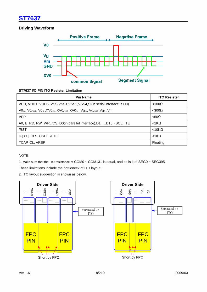
Driving Waveform
ST7637 I/O PIN ITO Resister Limitation
Pin Name ITO Resister
VDD, VDD1~VDD5, VSS,VSS1,VSS2,VSS4,SI(in serial interface is D0) <100Ω
V0IN, V0OUT, V0S ,XV0IN, XV0OUT ,XV0S , VgIN, VgOUT ,VgS ,Vm <300Ω
VPP <50Ω
A0, E_RD, RW_WR, /CS, D0(in parellel interface),D1, …D15, (SCL), TE <1KΩ
/RST <10KΩ
IF[3:1], CLS, CSEL, /EXT <1KΩ
TCAP, CL, VREF Floating
NOTE:
1. Make sure that the ITO resistance of COM0 ~ COM131 is equal, and so is it of SEG0 ~ SEG395.
These limitations include the bottleneck of ITO layout.
2. ITO layout suggestion is shown as below:
Separated by ITO
V0O
V0I
V0S
Driver Side
FPCPIN
FPCPIN
Short by FPC
V0I
VDD
VDD1
VDD2
Driver Side
VDDx
FPC
PIN
FPC
PIN
Short by FPC
Separated by ITO

ST7637
Ver 1.6 19/210 2009/03
7. FUNCTIONAL DESCRIPTION 7.1 MICROPROCESSOR INTERFACE Chip Select Input
/CS pin is chip selection. The ST7637 is active when /CS=L. In serial interface mode, the internal shift register and the
counter are reset when /CS=H.
7.2 Selecting Parallel / Serial Interface ST7637 has six types of interfaces with an MPU, which are two serial and four parallel interfaces. These parallel or serial
interfaces are determined by IF pin as shown in Table 7.2-1.
I/F Mode Pin Assignment
IF3 IF2 IF1 I/F Description
/CS A0 E_RD RW_WR Used Data Bus D1 D0
H H H 80 serial 16-bit parallel /CS A0 /RD /WR D15~D2 D1 D0
H H L 80 serial 8-bit parallel /CS A0 /RD /WR D7~D2 D1 D0
H L H 68 serial 16-bit parallel /CS A0 E R/W D15~D2 D1 D0
H L L 68 serial 8-bit parallel /CS A0 E R/W D7~D2 D1 D0
L H H 8-bit SPI mode (4 line) /CS SCL -- -- -- A0 SI
L H L 9-bit SPI mode (3 line) /CS SCL -- -- -- -- SI
Table 7.2-1 Parallel / Serial Interface Mode
NOTE: When these pins are set to any other combination, A0, E_RD and RW_WR inputs are disabled and D0
to D15 are to be high impedance.
7.2.1. 8-bit or 16-bit Parallel Interface
The ST7637 identifies the type of the data bus signals according to the combination of A0, /RD (E) and /WR (W/R) signals,
as shown in Table 7.2-2.
Common 6800-series 8080-series
A0 RW E /WR /RD Description
H H ↑ H ↓ Display data read out
H H ↑ H ↓ Register status read
L L ↓ ↑ H Instruction write
H L ↓ ↑ H Display data write
Table 7.2-2 Parallel Data Transfer

ST7637
Ver 1.6 20/210 2009/03
Figure 7.2-3 Parallel Data Transfer Example Chart
Relation between Data Bus and Gradation Data
ST7637 offers 256 color, 4096 color display, 65K color display, and truncated 262K color display, truncated 16M color
display. When using 256 colors, 4096, 65K, 262K, and 16M color display; you can specify color for each of R, G, and B
using the palette function. Use the command for switching between these modes.
(1) 256 color input mode
1. 8-bit interface
D7, D6, D5, D4, D3, D2, D1, D0: RRRGGGBB 1st -write
There is only 1 write operation for 1 pixel data.
1 pixel data is written in the display data RAM when 1st -write operation finishes.
(2) 4096-color display
(1-1) Type A 4096 color display
1. 8-bit mode
D7, D6, D5, D4, D3, D2, D1, D0: RRRRGGGG 1st-write
D7, D6, D5, D4, D3, D2, D1, D0: BBBB RRRR 2nd-write
D7, D6, D5, D4, D3, D2, D1, D0: GGGGBBBB 3rd-write

ST7637
Ver 1.6 21/210 2009/03
There are 3 write operations for 2 pixel data.
1st pixel data is written in the display data RAM when 2nd –write operation finishes, and 2nd pixel data is written in the
display data RAM when 3rd–write operation finishes.
2. 16-bit mode
D15, D14, D13, D12, D11, D10, D9, D8, D7, D6, D5, D4, D3, D2, D1, D0: RRRRGGGGBBBB XXXX 1st-write
There is only 1 write operation for 1 pixel data.
1 pixel data is written in the display data RAM when 1st –write operation finishes. “X” are ignored dummy bits.
(1-2) Type B 4096 color display
1. 8-bit mode
D7, D6, D5, D4, D3, D2, D1, D0: XXXXRRRR 1st-write
D7, D6, D5, D4, D3, D2, D1, D0: GGGGBBBB 2nd-write
There are 2 write operations for 1 pixel data.
1st pixel data is written in the display data RAM when 2nd –write operation finishes. “X” are ignored dummy bits.
2. 16-bit mode
D15, D14, D13, D12, D11, D10, D9, D8, D7, D6, D5, D4, D3, D2, D1, D0: XXXXRRRRGGGGBBBB 1st-write
There is only 1 write operation for 1 pixel data.
1 pixel data is written in the display data RAM when 1st –write operation finishes. “X” are ignored dummy bits.
(3) 65K color input mode
1. 8-bit mode
D7, D6, D5, D4, D3, D2, D1, D0: RRRRRGGG 1st-write
D7, D6, D5, D4, D3, D2, D1, D0: GGGBBBBB 2nd-write
There are 2 write operations for 1 pixel data.
1st pixel data is written in the display data RAM when 2nd –write operation finishes.
2. 16-bit mode
D15, D14, D13, D12, D11, D10, D9, D8, D7, D6, D5, D4, D3, D2, D1, D0: RRRRRGGGGGGBBBBB
There is only 1 write operation for 1 pixel data.
1 pixel data is written in the display data RAM when 1st –write operation finishes.
(4) Truncated 262K color input mode
1. 8-bit mode
D7, D6, D5, D4, D3, D2, D1, D0: RRRRRRXX 1st-write
D7, D6, D5, D4, D3, D2, D1, D0: GGGGGGXX 2nd-write
ST7637
Ver 1.6 22/210 2009/03
D7, D6, D5, D4, D3, D2, D1, D0: BBBBBB XX 3rd-write
There are 3 write operations for 1 pixel data.
1st pixel data is written in the display data RAM when 3rd–write operation finishes. “X” are ignored dummy bits.
2. 16 bit mode
D15, D14, D13, D12, D11, D10, D9, D8, D7, D6, D5, D4, D3, D2, D1, D0: RRRRRRXXGGGGGGXX 1st-write
D15, D14, D13, D12, D11, D10, D9, D8, D7, D6, D5, D4, D3, D2, D1, D0: BBBBBB XXXXXXXXXXXX 2nd-write
There are 2 write operations for 1 pixel data.
1st pixel data is written in the display data RAM when 2nd –write operation finishes. “X” are ignored dummy bits.
(5) Truncated 16M color input mode
1. 8-bit mode
D7, D6, D5, D4, D3, D2, D1, D0: RRRRRRRR 1st-write
D7, D6, D5, D4, D3, D2, D1, D0: GGGGGGGG 2nd-write
D7, D6, D5, D4, D3, D2, D1, D0: BBBBBBBB 3rd-write
There are 3 write operations for 1 pixel data.
1st pixel data is written in the display data RAM when 3rd–write operation finishes. “X” are ignored dummy bits.
2. 16 bit mode
D15, D14, D13, D12, D11, D10, D9, D8, D7, D6, D5, D4, D3, D2, D1, D0: RRRRRRRRGGGGGGGG 1st-write
D15, D14, D13, D12, D11, D10, D9, D8, D7, D6, D5, D4, D3, D2, D1, D0: BBBBBBBB XXXXXXXX 2nd-write
There are 2 write operations for 1 pixel data.
1st pixel data is written in the display data RAM when 2nd –write operation finishes. “X” are ignored dummy bits.
NOTE: 7637 offer read DDRAM function only in 65K color mode.
ST7637
Ver 1.6 23/210 2009/03
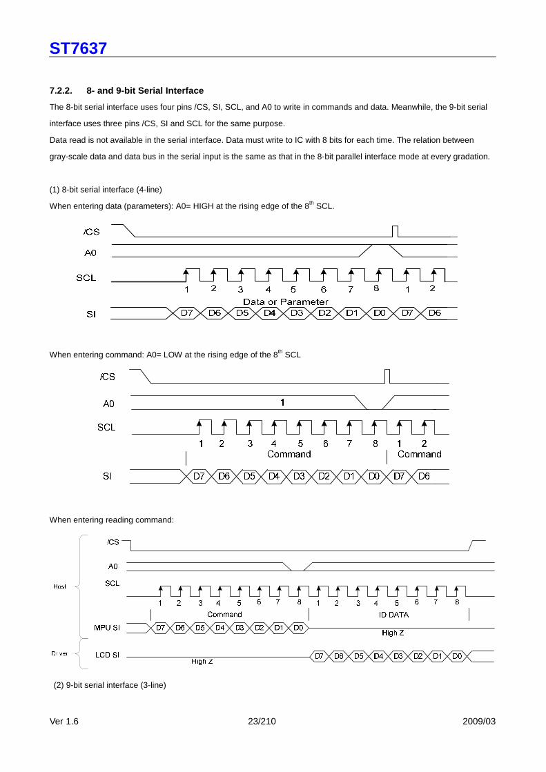
7.2.2. 8- and 9-bit Serial Interface
The 8-bit serial interface uses four pins /CS, SI, SCL, and A0 to write in commands and data. Meanwhile, the 9-bit serial
interface uses three pins /CS, SI and SCL for the same purpose.
Data read is not available in the serial interface. Data must write to IC with 8 bits for each time. The relation between
gray-scale data and data bus in the serial input is the same as that in the 8-bit parallel interface mode at every gradation.
(1) 8-bit serial interface (4-line)
When entering data (parameters): A0= HIGH at the rising edge of the 8th SCL.
When entering command: A0= LOW at the rising edge of the 8th SCL
When entering reading command:
(2) 9-bit serial interface (3-line)

ST7637
Ver 1.6 24/210 2009/03
When entering data (parameters): SI= HIGH at the rising edge of the 1st SCL.
When entering command: SI= LOW at the rising edge of the 1st SCL.
When entering reading command:
If /CS is set to HIGH while the 8 bits from D7 to D0 are entered, the data concerned is invalidated. Before entering
succeeding sets of data, you must correctly input the data concerned again.
In order to avoid data transfer error due to incoming noise, it is recommended to set /CS at HIGH on byte basis to
initialize the serial-to-parallel conversion counter and the register.

ST7637
Ver 1.6 25/210 2009/03
7.2.3. 8-bit and 9-bit Serial Interface Data Color Coding
8-bit serial interface (4-line)
(1) R 3-bit, G 3-bit, B 2-bit, 256 colors
There is 1 pixel ( = 3 sub-pixels ) per byte.
(2) R 4-bit, G 4-bit, B 4-bit, 4,096 colors — Type A
There are 2 pixel ( = 3 sub-pixels ) per 3 byte.

ST7637
Ver 1.6 26/210 2009/03
(3) R 4-bit, G 4-bit, B 4-bit, 4,096 colors — Type B
There is 1 pixel ( = 3 sub-pixels ) per 2 bytes.
(4) R 5-bit, G 6-bit, B 5-bit, 65,536 colors
There is 1 pixel ( = 3 sub-pixels ) per 2 byte.
ST7637
Ver 1.6 27/210 2009/03
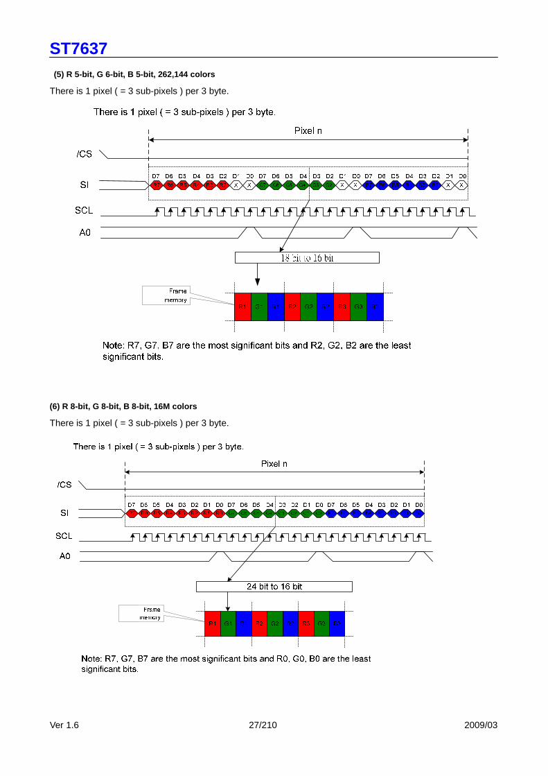
(5) R 5-bit, G 6-bit, B 5-bit, 262,144 colors
There is 1 pixel ( = 3 sub-pixels ) per 3 byte.
(6) R 8-bit, G 8-bit, B 8-bit, 16M colors
There is 1 pixel ( = 3 sub-pixels ) per 3 byte.

ST7637
Ver 1.6 28/210 2009/03
9-bit serial interface (3-line)
(1) R 3-bit, G 3-bit, B 2-bit, 256 colors
There is 1 pixel ( = 3 sub-pixels ) per byte.
(2) R 4-bit, G 4-bit, B 4-bit, 4,096 colors – Type A
There are 2 pixel ( = 3 sub-pixels ) per 3 byte.
R2 R1 R0 G3 G2 G1 G0R3 1 B3 B2 B1 B0 R3 R2 R1 R0 1 G3 G2 G2 G0 B31 B2 B1 B0
D7 D6 D5 D4 D3 D2 D1 D0 D7 D6 D5 D4 D3 D2 D1 D0 D7 D6 D5 D4 D3 D2 D1 D0
/CS
SI
SCL
Pixel n Pixel n+1
LUT (12 bit to 16 bit)
G1R1 B3G3R3B2G2R2B1
Frame
memory
Note: R3, G3, B3 are the most significant bits and R0, G0, B0 are the least
significant bits.
There are 2 pixel ( = 3 sub-pixels ) per 3 byte.

ST7637
Ver 1.6 29/210 2009/03
(3) R 4-bit, G 4-bit, B 4-bit, 4,096 colors – Type B
There is 1 pixel ( = 3 sub-pixels ) per 2 bytes.
(4) R 5-bit, G 6-bit, B 5-bit, 65,536 colors
There is 1 pixel ( = 3 sub-pixels ) per 2 byte.
ST7637
Ver 1.6 30/210 2009/03
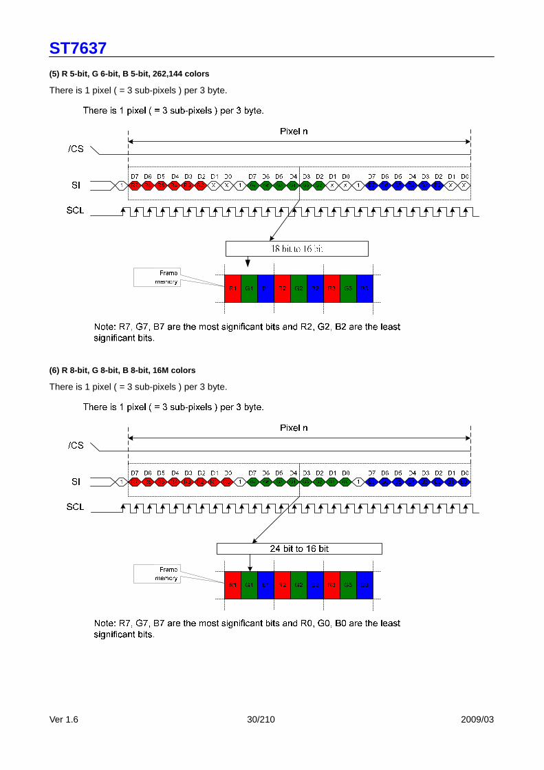
(5) R 5-bit, G 6-bit, B 5-bit, 262,144 colors
There is 1 pixel ( = 3 sub-pixels ) per 3 byte.
(6) R 8-bit, G 8-bit, B 8-bit, 16M colors
There is 1 pixel ( = 3 sub-pixels ) per 3 byte.
ST7637
Ver 1.6 31/210 2009/03
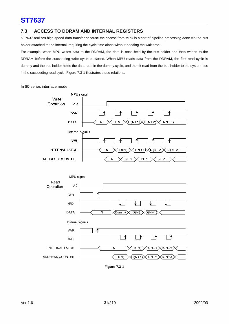
7.3 ACCESS TO DDRAM AND INTERNAL REGISTERS ST7637 realizes high-speed data transfer because the access from MPU is a sort of pipeline processing done via the bus
holder attached to the internal, requiring the cycle time alone without needing the wait time.
For example, when MPU writes data to the DDRAM, the data is once held by the bus holder and then written to the
DDRAM before the succeeding write cycle is started. When MPU reads data from the DDRAM, the first read cycle is
dummy and the bus holder holds the data read in the dummy cycle, and then it read from the bus holder to the system bus
in the succeeding read cycle. Figure 7.3-1 illustrates these relations.
In 80-series interface mode:
N Dummy D(N) D(N+1)
MPU signal
A0
DATA
Internal signals
ADDRESS COUNTER
/RD
N D(N) D(N+1) D(N+2)
D(N+3)
INTERNAL LATCH
Read
Operation
/WR
/WR
/RD
D(N) D(N+1) D(N+2)
Figure 7.3-1

ST7637
Ver 1.6 32/210 2009/03
7.4 DISPLAY DATA RAM (DDRAM) 7.4.1. DDRAM
It is 132 X 132 X 16 bits capacity RAM prepared for storing dot data. Refer to the following memory map for the RAM
configuration.
Memory Map
RGB alignment Data control command Column
0 1 131 (MADCTR) MX=0
131 130 0 (MADCTR) MX=1
Color R G B R G B R G B
Data
Page
(MADCTR)
MY=0
(MADCTR)
MY=1
0 131
1 130
2 129
3 128
4 127
5 126
6 125
7 124
: :
124 7
125 6
126 5
127 4
128 3
129 2
130 1
131
0
SEGout 0 1 2 3 4 5 393 394 395
You can change position of R and B with MADCTR command.
ST7637
Ver 1.6 33/210 2009/03
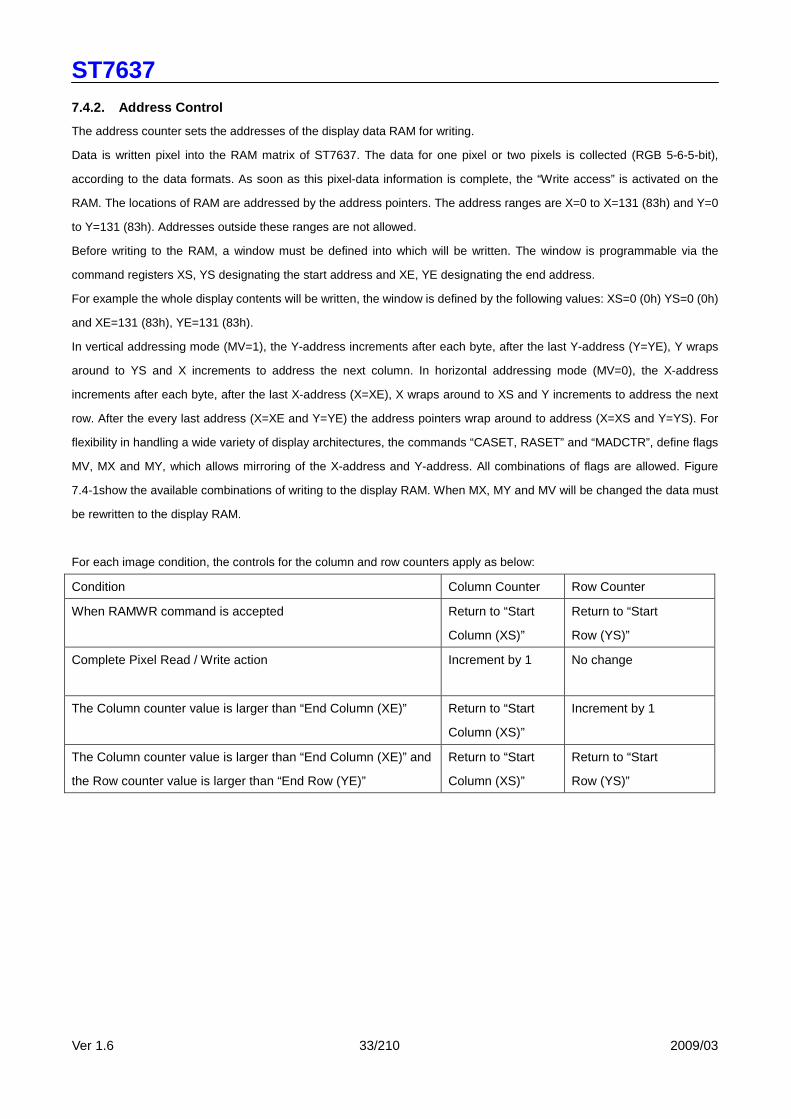
7.4.2. Address Control
The address counter sets the addresses of the display data RAM for writing.
Data is written pixel into the RAM matrix of ST7637. The data for one pixel or two pixels is collected (RGB 5-6-5-bit),
according to the data formats. As soon as this pixel-data information is complete, the “Write access” is activated on the
RAM. The locations of RAM are addressed by the address pointers. The address ranges are X=0 to X=131 (83h) and Y=0
to Y=131 (83h). Addresses outside these ranges are not allowed.
Before writing to the RAM, a window must be defined into which will be written. The window is programmable via the
command registers XS, YS designating the start address and XE, YE designating the end address.
For example the whole display contents will be written, the window is defined by the following values: XS=0 (0h) YS=0 (0h)
and XE=131 (83h), YE=131 (83h).
In vertical addressing mode (MV=1), the Y-address increments after each byte, after the last Y-address (Y=YE), Y wraps
around to YS and X increments to address the next column. In horizontal addressing mode (MV=0), the X-address
increments after each byte, after the last X-address (X=XE), X wraps around to XS and Y increments to address the next
row. After the every last address (X=XE and Y=YE) the address pointers wrap around to address (X=XS and Y=YS). For
flexibility in handling a wide variety of display architectures, the commands “CASET, RASET” and “MADCTR”, define flags
MV, MX and MY, which allows mirroring of the X-address and Y-address. All combinations of flags are allowed. Figure
7.4-1show the available combinations of writing to the display RAM. When MX, MY and MV will be changed the data must
be rewritten to the display RAM.
For each image condition, the controls for the column and row counters apply as below:
Condition Column Counter Row Counter
When RAMWR command is accepted Return to “Start
Column (XS)”
Return to “Start
Row (YS)”
Complete Pixel Read / Write action Increment by 1 No change
The Column counter value is larger than “End Column (XE)” Return to “Start
Column (XS)”
Increment by 1
The Column counter value is larger than “End Column (XE)” and
the Row counter value is larger than “End Row (YE)”
Return to “Start
Column (XS)”
Return to “Start
Row (YS)”

ST7637
Ver 1.6 34/210 2009/03
MADCTR
Parameter
Display
Data
Direction MV MX MY
Image in the Host
(MPU)
Image in the Driver
(DDRAM)
Normal 0 0 0
Y-Mirror 0 0 1
X-Mirror 0 1 0
X-Mirror
Y-Mirror
0 1 1
X-Y
Exchange
1 0 0
X-Y
Exchange
Y-Mirror
1 0 1
X-Y
Exchange
X-Mirror
1 1 0
X-Y
Exchange
X-Mirror
Y-Mirror
1 1 1
Figure 7.4-1 Frame Data Write Direction According t o the MADCTR parameters (MV, MX and MY)

ST7637
Ver 1.6 35/210 2009/03
7.4.3. I/O Buffer Circuit
It is the bi-directional buffer used when MPU reads or writes the DDRAM. Since MPU’s read or write of DDRAM is
performed independently from data output to the display data latch circuit, asynchronous access to the DDRAM when the
LCD is turned on does not cause troubles such as flicking of the display images.
7.4.4. Scroll Address Circuit
The circuit associates lines on DDRAM with COM output. ST7637 processes signals for the liquid crystal display on 1-line
basis. Thus, when specifying a specific area in the area scroll display or partial display, you must designate it in line.
7.4.5. Display data Latch Circuit
This circuit is used to temporarily hold display data to be output from the DDRAM to the SEG decoder circuit. Since display
normal/inverse and display on/off commands are used to control data in the latch circuit alone, they do not modify data in
the DDRAM.

ST7637
Ver 1.6 36/210 2009/03
7.4.6. Normal Display On or Partial Mode On, Verti cal Scroll Off
In this mode, contents of the frame memory within an area where column address is 00h to 83h and row address is 00h to
83h is displayed.
To display a dot on leftmost top corner, store the dot data at (column address, row address) = (0,0).
Example1) Normal Display On
SEG0
: ::
SEG4
SEG3
SEG2
SEG1
SEG131
SEG130
SEG129
SEG128
:
Example2) Partial Display On: PSL[6:0] = 04h, PEL[6:0] = 80h, MADCTR (ML)=0
SEG0
: ::
SEG4
SEG3
SEG2
SEG1
SEG131
SEG130
SEG129
SEG128
:

ST7637
Ver 1.6 37/210 2009/03
7.4.7. Vertical Scroll/Rolling Scroll
7.4.7.1. Rolling Scroll
There is just one types of vertical scrolling, which are determined by the commands “Vertical Scrolling Definition” (33h) and
“Vertical Scrolling Start Address” (37h).
Figure 7.4-2 Rolling Scroll Definition
When Vertical Scrolling Definition Parameters (TFA+VSA+BFA) =132. In this case, ‘rolling’ scrolling is applied as shown
below. All the memory contents will be used.
Example1) Panel size=132 x 132, TFA =3, VSA=127, BFA=2, SSA=4, MADCTR ML=0: Rolling Scroll

ST7637
Ver 1.6 38/210 2009/03
Example2) Panel size=132 x 132, TFA =3, VSA=127, BFA=2, SSA=4, MADCTR ML=1: Rolling Scroll (TFA and BFA are exchanged)
7.4.7.2. Vertical Scroll Example
There are 2 types of vertical scrolling, which are determined by the commands “Vertical Scrolling Definition” (33h) and
“Vertical Scrolling Start Address” (37h).
Case 1: TFA + VSA + BFA<132
N/A. Do not set TFA + VSA + BFA<132. In that case, unexpected picture will be shown.
Case 2: TFA + VSA + BFA=132 (Rolling Scrolling)
Example1) When MADCTR parameter ML=”0”, TFA=0, VSA=132, BFA=0 and VSCSAD=40.
1
21
1 21
22
ST7637
Ver 1.6 39/210 2009/03
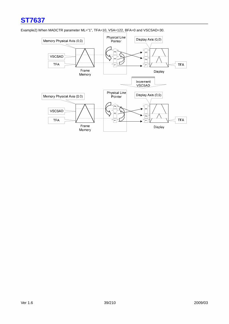
Example2) When MADCTR parameter ML=”1”, TFA=10, VSA=122, BFA=0 and VSCSAD=30.
11
21
23
3
13
23
2

ST7637
Ver 1.6 40/210 2009/03
7.4.8. Tearing Effect Output Line
The Tearing Effect output line supplies to the MPU a Panel synchronization signal. This signal can be enabled or disabled
by the Tearing Effect Line Off & On commands. The signal can be used by the MPU to synchronize Frame Memory Writing
when displaying video images.
7.4.8.1. Tearing Effect Line Modes
Mode 1 , the Tearing Effect Output signal consists of V-Sync (tVHD) information. It starts at 124th line signal and ends at
the 132th line signal. There is one high pulse during each frame.
Mode 2 , the Tearing Effect Output signal consists of both H-Sync(tHDH) and V-Sync(tVDH) information. TE pin outputs
tHDH pulse on each COM scan signal. During 124th ~ 132th line signal, it output a high pulse which equals:
1 tHDH + 1 tVDH.
Note: During Sleep In Mode, the Tearing Effect Output Pin is active Low.

ST7637
Ver 1.6 41/210 2009/03
7.4.8.2. Tearing Effect Line Timing
The Tearing Effect signal is described below:
Figure 7.4-3 AC characteristics of Tearing Effect Sig nal
Idle Mode Off (Frame Rate = 77Hz)
Symbol Parameter Min Typ Max Unit Description
tVDL Vertical Timing Low Duration -- 11.4 -- ms
tVDH Vertical Timing High Duration 1 1.6 -- ms Mode1
tHDL Horizontal Timing Low Duration - 92 -- us
tHDH Horizontal Timing High Duration 3 6 -- us Mode2
Note: The signal’s rise and fall times (tf, tr) are stipulated to be equal to or less than 15ns.

ST7637
Ver 1.6 42/210 2009/03
Example 1: MPU Write is faster than Panel Read.
Data write to Frame Memory is now synchronized to the Panel Scan. It should be written during the vertical sync pulse of
the Tearing Effect Output Line. This ensures that data is always written ahead of the panel scan and each Panel Frame
refresh has a complete new image:
ST7637
Ver 1.6 43/210 2009/03
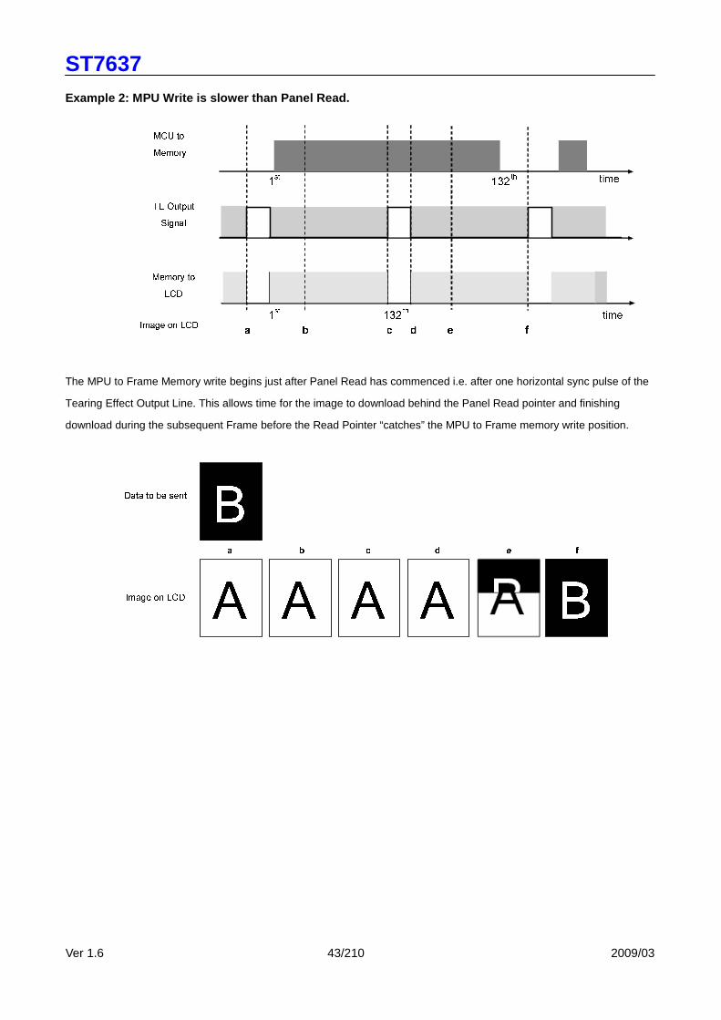
Example 2: MPU Write is slower than Panel Read.
The MPU to Frame Memory write begins just after Panel Read has commenced i.e. after one horizontal sync pulse of the
Tearing Effect Output Line. This allows time for the image to download behind the Panel Read pointer and finishing
download during the subsequent Frame before the Read Pointer “catches” the MPU to Frame memory write position.

ST7637
Ver 1.6 44/210 2009/03
7.5 Gray-Scale Display ST7637 incorporates a 4FRC & 31 PWM function circuit to display a 64 gray-scale display.
7.6 Oscillation circuit ST7637 is built-in an oscillator circuit. It provides internal clock without external resistor. This oscillator signal is used in the
voltage converter and display timing generation circuit.
7.7 Display Timing Generator Circuit This circuit generates some signals to be used for displaying LCD. The display clock , which is generated by oscillation
clock, generates the clock for the line counter and the signal for the display data latch. The line address of on-chip RAM is
generated in synchronization with the display clock and the display data latch circuit latches the 132-bits display data in
synchronization with the display clock. The display data, which is read to the LCD driver, is completely independent of the
access to the display data RAM from the microprocessor. The display clock generates an LCD AC signal (M), which
enables the LCD driver to make an AC drive waveform, and also generates an internal common timing signal and start
signal to the common driver. The frame signal or the line signal changes the M by setting internal instruction. Driving
waveform and internal timing signal are shown in Figure 7.7-1.
Figure 7.7-1 2-frame AC Driving Waveform (Duty Rati o: 1/132)
ST7637
Ver 1.6 45/210 2009/03
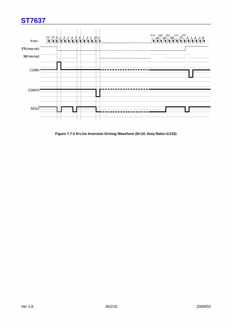
Figure 7.7-2 N-Line Inversion Driving Waveform (N=1 0, Duty Ratio=1/132)

ST7637
Ver 1.6 46/210 2009/03
7.8 POWER LEVEL DEFINITION 7.8.1. Power ON/OFF SEQUENCE
NOTE: VDDI=VDD, VDD1; VDDA=VDD2, VDD3, VDD4, VDD5
During power off, if LCD is in the Sleep Out mode, VDDA and VDDI must be powered down minimum 120msec after /RST
has been released.
During power off, if LCD is in the Sleep In mode, VDDI or VDDA can be powered down minimum 0msec after /RST has
been released.
/CS can be applied at any timing or can be permanently grounded. /RST has priority over /CS.
If /RST line is not held stable by host during Power On Sequence as defined in Sections case1 and case2, then it will be
necessary to apply a Hardware Reset (/RST) after Host Power On Sequence is complete to ensure correct operation.
Otherwise function is not guaranteed.
The power on/off sequence is illustrated below:
Case 1 – /RST line is held High or Unstable by Host at Power On
If /RST line is held High or unstable by the host during Power On, then a Hardware Reset must be applied after both VDDA
and VDDI have been applied – otherwise correct functionality is not guaranteed. There is no timing restriction upon this
hardware reset.
Note: Unless otherwise specified, timings herein show cross point at 50% of signal/power level.
Case 2 – /RST line is held Low by host at Power On
If /RST line is held Low (and stable) by the host during Power On, then the /RST must be held low for minimum 10µsec
after both VDDA and VDDI have been applied.

ST7637
Ver 1.6 47/210 2009/03
Note: Unless otherwise specified, timings herein show cross point at 50% of signal/power level.

ST7637
Ver 1.6 48/210 2009/03
7.8.2. Power Levels
6 level modes are defined they are in order of Maximum Power consumption to Minimum Power
Consumption:
1. Normal Mode On (full display), Idle Mode Off, Sl eep Out:
In this mode, the display is able to show maximum 65K colors.
2. Partial Mode On, Idle Mode Off, Sleep Out:
In this mode part of the display is used with maximum 65K colors.
3. Normal Mode On (full display), Idle Mode On, Sle ep Out:
In this mode, the full display area is used but with 8 colors.
4. Partial Mode On, Idle Mode On, Sleep Out:
In this mode, part of the display is used but with 8 colors.
5. Sleep In Mode:
In this mode, the DC:DC converter, internal oscillator and panel driver circuit are stopped. Only the MCU
interface and memory works with Digital VDD power supply. Contents of the memory are safe.
6. Power Off Mode:
In this mode, both Analog VDD and Digital VDDI are removed.
Note: Transition between modes 1-5 is controllable by MCU commands. Mode 6 is entered only when both
Power supplies are removed.
ST7637
Ver 1.6 49/210 2009/03
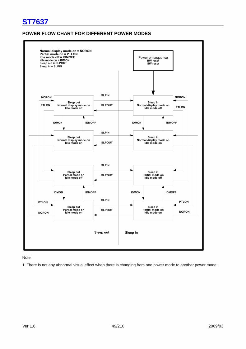
POWER FLOW CHART FOR DIFFERENT POWER MODES
Power on sequenceHW resetSW reset
Sleep inNormal display mode on
Idle mode off
Sleep inNormal display mode on
Idle mode on
Sleep inPartial mode onIdle mode off
Sleep inPartial mode onIdle mode on
Sleep outNormal display mode on
Idle mode off
Sleep outNormal display mode on
Idle mode on
Sleep outPartial mode onIdle mode off
Sleep outPartial mode onIdle mode on
Normal display mode on = NORONPartial mode on = PTLONIdle mode off = IDMOFFIdle mode on = IDMONSleep out = SLPOUT
Sleep in = SLPIN
NORON
PTLON
SLPIN
SLPOUT
SLPIN
SLPOUT
SLPIN
SLPOUT
SLPIN
SLPOUT
PTLON
NORON
NORON
PTLON
PTLON
NORON
IDMON IDMOFF
IDMON IDMOFFIDMON IDMOFF
IDMON IDMOFF
Sleep out Sleep in
Note
1: There is not any abnormal visual effect when there is changing from one power mode to another power mode.

ST7637
Ver 1.6 50/210 2009/03
7.9 Color Depth Conversion Look Up Table
Look Up Table Input Color 256 Color Data
8-bit/pixel 4K Color Data
12-bit/pixel
Look Up Table Outputs (16-bit/pixel) Frame Memory Data (5 or 6-bit)
Default Value
RGBSET Parameter
000 0000 R004 R003 R002 R001 R000 00000 1 001 0001 R014 R013 R012 R011 R010 00010 2 010 0010 R024 R023 R022 R021 R020 00100 3 011 0011 R034 R033 R032 R031 R030 00110 4 100 0100 R044 R043 R042 R041 R040 01000 5 101 0101 R054 R053 R052 R051 R050 01010 6 110 0110 R064 R063 R062 R061 R060 01100 7 111 0111 R074 R073 R072 R071 R070 01110 8
1000 R084 R083 R082 R081 R080 10000 9 1001 R094 R093 R092 R091 R090 10010 10 1010 R104 R103 R102 R101 R100 10100 11 1011 R114 R113 R112 R111 R110 10110 12 1100 R124 R123 R122 R121 R120 11000 13 1101 R134 R133 R132 R131 R130 11010 14 1110 R144 R143 R142 R141 R140 11100 15
Red
Dummy input
1111 R154 R153 R152 R151 R150 11111 16 000 0000 G005 G004 G003 G002 G001 G000 000000 17 001 0001 G015 G014 G013 G012 G011 G010 000100 18 010 0010 G025 G024 G023 G022 G021 G020 001000 19 011 0011 G035 G034 G033 G032 G031 G030 001100 20 100 0100 G045 G044 G043 G042 G041 G040 010000 21 101 0101 G055 G054 G053 G052 G051 G050 010100 22 110 0110 G065 G064 G063 G062 G061 G060 011000 23 111 0111 G075 G074 G073 G072 G071 G070 011100 24
1000 G085 G084 G083 G082 G081 G080 100000 25 1001 G095 G094 G093 G092 G091 G090 100100 26 1010 G105 G104 G103 G102 G101 G100 101000 27 1011 G115 G114 G113 G112 G111 G110 101100 28 1100 G125 G124 G123 G122 G121 G120 110000 29 1101 G135 G134 G133 G132 G131 G130 110100 30 1110 G145 G144 G143 G142 G141 G140 111000 31
Green
Dummy input
1111 G155 G154 G153 G152 G151 G150 111111 32 00 0000 B004 B003 B002 B001 B000 00000 33 01 0001 B014 B013 B012 B011 B010 00010 34 10 0010 B024 B023 B022 B021 B020 00100 35 11 0011 B034 B033 B032 B031 B030 00110 36
0100 B044 B043 B042 B041 B040 01000 37 0101 B054 B053 B052 B051 B050 01010 38 0110 B064 B063 B062 B061 B060 01100 39 0111 B074 B073 B072 B071 B070 01110 40 1000 B084 B083 B082 B081 B080 10000 41 1001 B094 B093 B092 B091 B090 10010 42 1010 B104 B103 B102 B101 B100 10100 43 1011 B114 B113 B112 B111 B110 10110 44 1100 B124 B123 B122 B121 B120 11000 45 1101 B134 B133 B132 B131 B130 11010 46 1110 B144 B143 B142 B141 B140 11100 47
Blue
Dummy input
1111 B154 B153 B152 B151 B150 11111 48
ST7637
Ver 1.6 51/210 2009/03
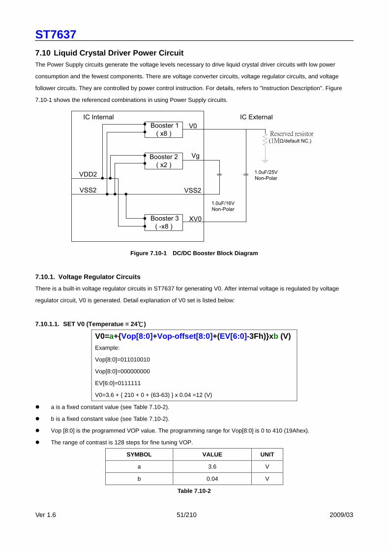
7.10 Liquid Crystal Driver Power Circuit The Power Supply circuits generate the voltage levels necessary to drive liquid crystal driver circuits with low power
consumption and the fewest components. There are voltage converter circuits, voltage regulator circuits, and voltage
follower circuits. They are controlled by power control instruction. For details, refers to "Instruction Description". Figure
7.10-1 shows the referenced combinations in using Power Supply circuits.
Booster 2
( x2 )
Booster 1
( x8 )
Booster 3
( -x8 )
V0
Vg
XV0
VSS2
1.0uF/25V
Non-Polar
1.0uF/16V
Non-Polar
IC Internal IC External
VSS2
VDD2
Reserved resistor(1MΩ/default NC.)
Figure 7.10-1 DC/DC Booster Block Diagram
7.10.1. Voltage Regulator Circuits
There is a built-in voltage regulator circuits in ST7637 for generating V0. After internal voltage is regulated by voltage
regulator circuit, V0 is generated. Detail explanation of V0 set is listed below:
7.10.1.1. SET V0 (Temperatue = 24 )
V0=a+Vop[8:0] +Vop-offset[8:0] +(EV[6:0] -3Fh)x b (V)
Example:
Vop[8:0]=011010010
Vop[8:0]=000000000
EV[6:0]=0111111
V0=3.6 + 210 + 0 + (63-63) x 0.04 =12 (V)
a is a fixed constant value (see Table 7.10-2).
b is a fixed constant value (see Table 7.10-2).
Vop [8:0] is the programmed VOP value. The programming range for Vop[8:0] is 0 to 410 (19Ahex).
The range of contrast is 128 steps for fine tuning VOP.
SYMBOL VALUE UNIT
a 3.6 V
b 0.04 V
Table 7.10-2
ST7637
Ver 1.6 52/210 2009/03
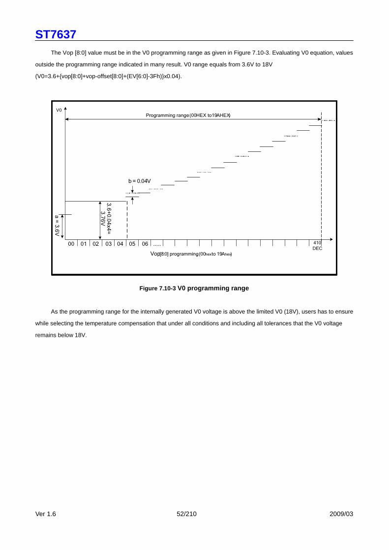
The Vop [8:0] value must be in the V0 programming range as given in Figure 7.10-3. Evaluating V0 equation, values
outside the programming range indicated in many result. V0 range equals from 3.6V to 18V
(V0=3.6+vop[8:0]+vop-offset[8:0]+(EV[6:0]-3Fh)x0.04).
00 01 02 03 04 05 06 ..... 410
DEC
b = 0.04V
3.6+0.04x4=
3.76V
V0Programming range(00HEX to19AHEX)
Vop[8:0] programming, (00hexto 19Ahex)
a=3.6V
Figure 7.10-3 V0 programming range
As the programming range for the internally generated V0 voltage is above the limited V0 (18V), users has to ensure
while selecting the temperature compensation that under all conditions and including all tolerances that the V0 voltage
remains below 18V.
ST7637
Ver 1.6 53/210 2009/03
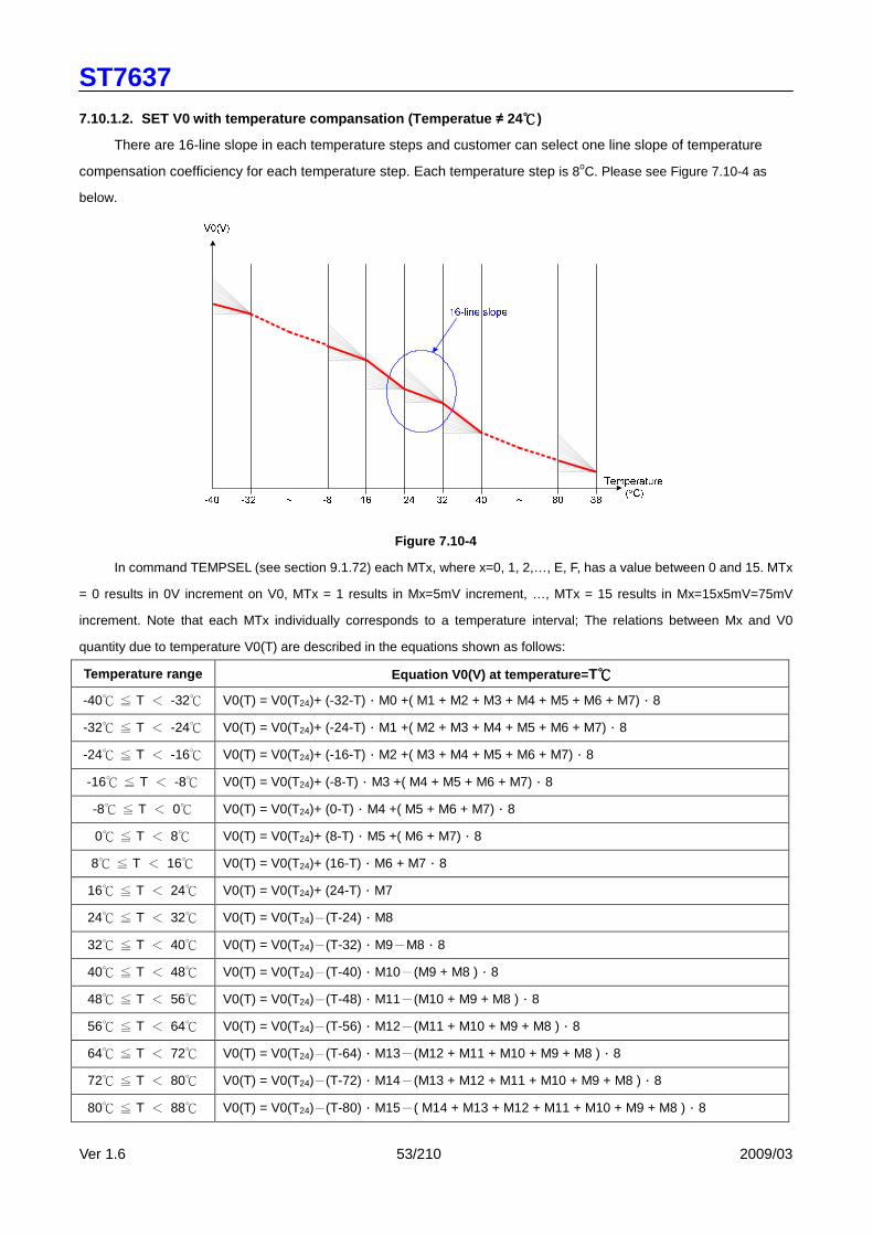
7.10.1.2. SET V0 with temperature compansation (Tem peratue ≠ 24 )
There are 16-line slope in each temperature steps and customer can select one line slope of temperature
compensation coefficiency for each temperature step. Each temperature step is 8oC. Please see Figure 7.10-4 as
below.
Figure 7.10-4
In command TEMPSEL (see section 9.1.72) each MTx, where x=0, 1, 2,…, E, F, has a value between 0 and 15. MTx
= 0 results in 0V increment on V0, MTx = 1 results in Mx=5mV increment, …, MTx = 15 results in Mx=15x5mV=75mV
increment. Note that each MTx individually corresponds to a temperature interval; The relations between Mx and V0
quantity due to temperature V0(T) are described in the equations shown as follows:
Temperature range Equation V0(V) at temperature= T
-40 T < -32 V0(T) = V0(T24)+ (-32-T).M0 +( M1 + M2 + M3 + M4 + M5 + M6 + M7).8
-32 T < -24 V0(T) = V0(T24)+ (-24-T).M1 +( M2 + M3 + M4 + M5 + M6 + M7).8
-24 T < -16 V0(T) = V0(T24)+ (-16-T).M2 +( M3 + M4 + M5 + M6 + M7).8
-16 T < -8 V0(T) = V0(T24)+ (-8-T).M3 +( M4 + M5 + M6 + M7).8
-8 T < 0 V0(T) = V0(T24)+ (0-T).M4 +( M5 + M6 + M7).8
0 T < 8 V0(T) = V0(T24)+ (8-T).M5 +( M6 + M7).8
8 T < 16 V0(T) = V0(T24)+ (16-T).M6 + M7.8
16 T < 24 V0(T) = V0(T24)+ (24-T).M7
24 T < 32 V0(T) = V0(T24)-(T-24).M8
32 T < 40 V0(T) = V0(T24)-(T-32).M9-M8.8
40 T < 48 V0(T) = V0(T24)-(T-40).M10-(M9 + M8 ).8
48 T < 56 V0(T) = V0(T24)-(T-48).M11-(M10 + M9 + M8 ).8
56 T < 64 V0(T) = V0(T24)-(T-56).M12-(M11 + M10 + M9 + M8 ).8
64 T < 72 V0(T) = V0(T24)-(T-64).M13-(M12 + M11 + M10 + M9 + M8 ).8
72 T < 80 V0(T) = V0(T24)-(T-72).M14-(M13 + M12 + M11 + M10 + M9 + M8 ).8
80 T < 88 V0(T) = V0(T24)-(T-80).M15-( M14 + M13 + M12 + M11 + M10 + M9 + M8 ).8
ST7637
Ver 1.6 54/210 2009/03
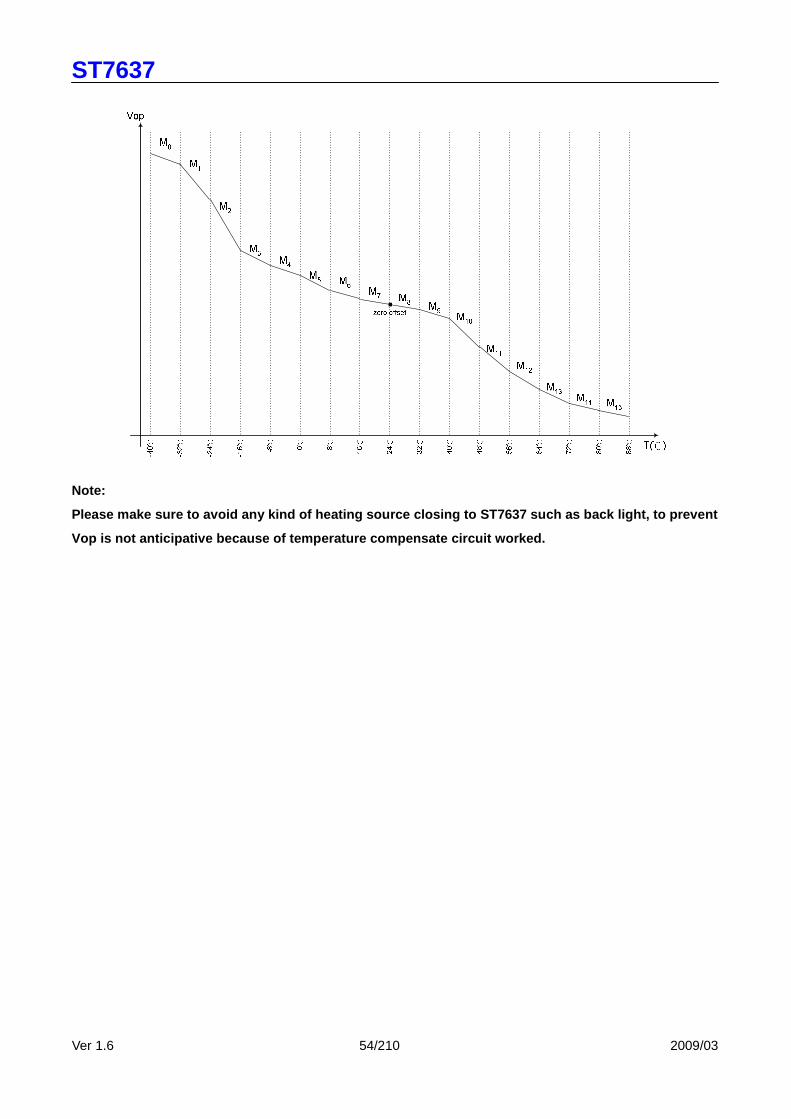
Note:
Please make sure to avoid any kind of heating sourc e closing to ST7637 such as back light, to prevent
Vop is not anticipative because of temperature comp ensate circuit worked.
ST7637
Ver 1.6 55/210 2009/03
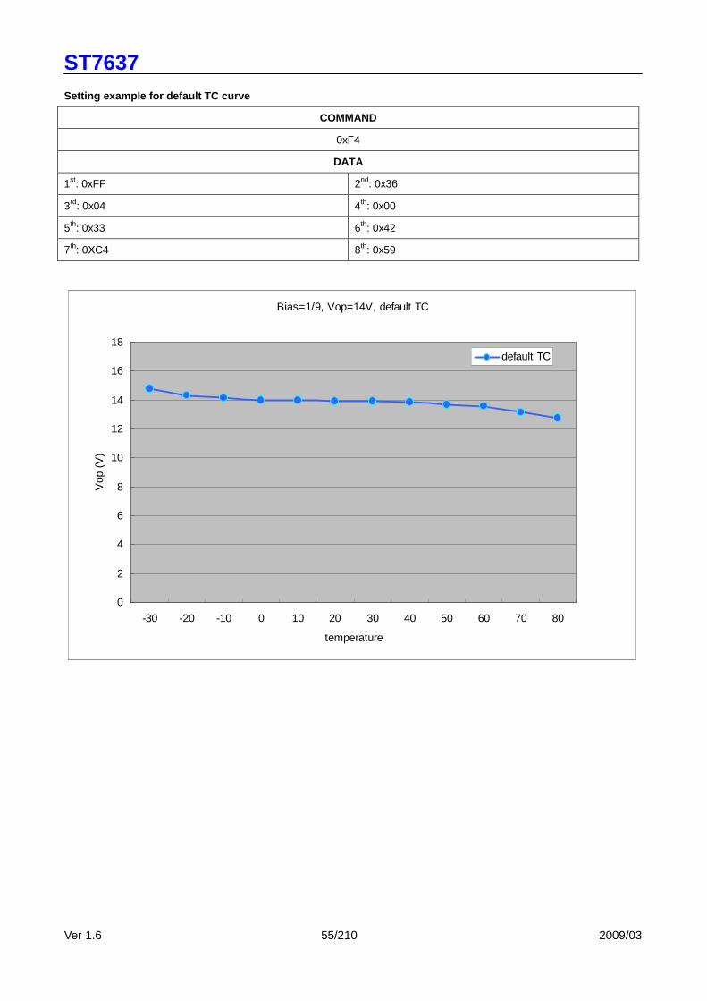
Setting example for default TC curve
COMMAND
0xF4
DATA
1st: 0xFF 2nd: 0x36
3rd: 0x04 4th: 0x00
5th: 0x33 6th: 0x42
7th: 0XC4 8th: 0x59
Bias=1/9, Vop=14V, default TC
0
2
4
6
8
10
12
14
16
18
-30 -20 -10 0 10 20 30 40 50 60 70 80
temperature
Vop
(V
)
default TC

ST7637
Ver 1.6 56/210 2009/03
Setting example for TC curve=-0.06%/
COMMAND
0xF4
DATA
1st: 0x33 2nd: 0x33
3rd: 0x33 4th: 0x33
5th: 0x33 6th: 0x33
7th: 0x33 8th: 0x33
Bias=1/9, Vop=14, TC=-0.06%/
0
2
4
6
8
10
12
14
16
18
-30 -20 -10 0 10 20 30 40 50 60 70 80
temperature
Vop
(V
)
-0.06%
ST7637
Ver 1.6 57/210 2009/03
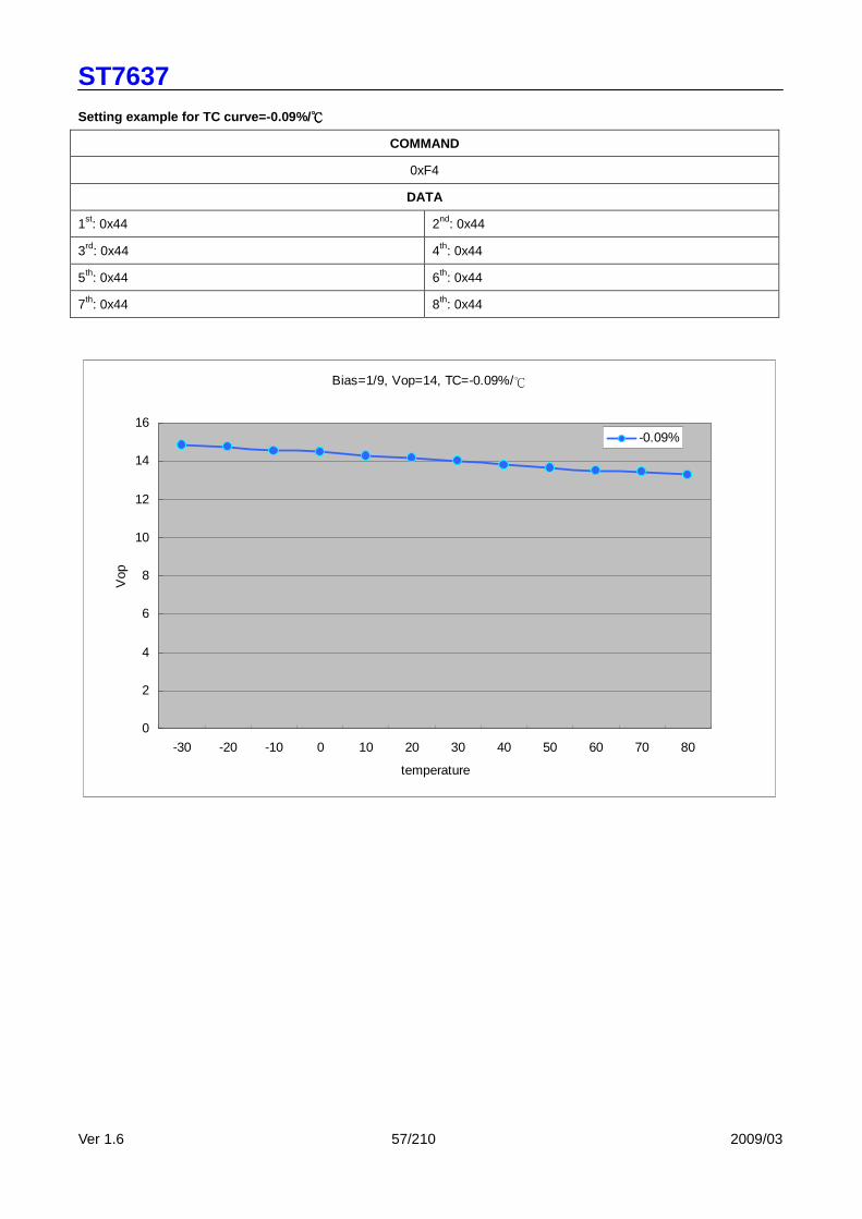
Setting example for TC curve=-0.09%/
COMMAND
0xF4
DATA
1st: 0x44 2nd: 0x44
3rd: 0x44 4th: 0x44
5th: 0x44 6th: 0x44
7th: 0x44 8th: 0x44
Bias=1/9, Vop=14, TC=-0.09%/
0
2
4
6
8
10
12
14
16
-30 -20 -10 0 10 20 30 40 50 60 70 80
temperature
Vop
-0.09%

ST7637
Ver 1.6 58/210 2009/03
Setting example for TC curve=-0.15%/
COMMAND
0xF4
DATA
1st: 0x55 2nd: 0x55
3rd: 0x55 4th: 0x55
5th: 0x55 6th: 0x55
7th: 0x55 8th: 0x55
Bias=1/9, Vop=14V,TC=-0.15%
0
2
4
6
8
10
12
14
16
-30 -20 -10 0 10 20 30 40 50 60 70 80
temperature
Vop
(V
)
TC=-0.15%

ST7637
Ver 1.6 59/210 2009/03
7.10.1.3. V0 fine tuning
ST7637 has 2 commands for fine tuning V0. These commands are VopOfsetInc (see section 9.1.47) and
VopOfsetDec (see section 9.1.48). When writing VopOfsetInc into IC for each time, V0 would increase 40mV; when writing
VopOfsetDec into IC for each time, V0 would decrease 40mV.
Example:
Vop[8:0]=011010010
EV[6:0]=0111111
VopOfsetInc x2
→ V0=3.6 + 210 + (63-63) x 0.04 + 0.04x2 =12.08 (V)
7.10.2. Voltage Follower Circuits
There is a build-in voltage follower circuits in ST7637 for generating Vg and Vm. These voltages are decided by bias
ratio selection circuitry which is set by users with software to control 1/5 to 1/12 bias ratios to match the optimum display
performance of LCD panel. Bias driving rule is listed below:
LCD bias Vg Vm
1/N bias (2/N) x V0 (1/N) x V0
N=5 to 12
7.10.3. OTP Setting Flow
ST7637 provides the Write and Read function to write the electronic control value and built-in resistance
ratio into built-in OTP, and then read them from it. Using the Write and Read functions, you can store these
values appropriate to each LCD panel. This function is very convenient for user in setting from some different
panel’s voltage. But using this function must attention the setting procedure. Please see the following diagram.
Figure 7.10-5 V0 value control for different module s by loading Vop offset
Note1: This setting flow is used for LCM assembler.
Note2: OTP shouldn’t be written without preceding loading correctly from OTP in order to avoid some errors
during IC operation.
ST7637
Ver 1.6 60/210 2009/03
Note3: When writing value to OTP, the voltage of VPP must be more than 7.5V (7.5V~7.75V); the current of
Ivpp must be more than 4 mA.
Note4: If the OTP is exposed to a high temperature for hours, data in the memory cell may probably be lost
before the data retention guarantee period. To retain data in the memory cell, keep the memory cell below
90. The data retention guarantee period is specified including the retention period.
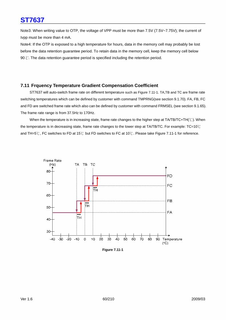
7.11 Frquency Temperature Gradient Compensation Coe fficient ST7637 will auto-switch frame rate on different temperature such as Figure 7.11-1. TA,TB and TC are frame rate
switching temperatures which can be defined by customer with command TMPRNG(see section 9.1.70). FA, FB, FC
and FD are switched frame rate which also can be defined by customer with command FRMSEL (see section 9.1.65).
The frame rate range is from 37.5Hz to 170Hz.
When the temperature is in increasing state, frame rate changes to the higher step at TA/TB/TC+TH( ). When
the temperature is in decreasing state, frame rate changes to the lower step at TA/TB/TC. For example: TC=10
and TH=5 , FC switches to FD at 15 but FD switches to FC at 10 . Please take Figure 7.11-1 for reference.
Figure 7.11-1
ST7637
Ver 1.6 61/210 2009/03
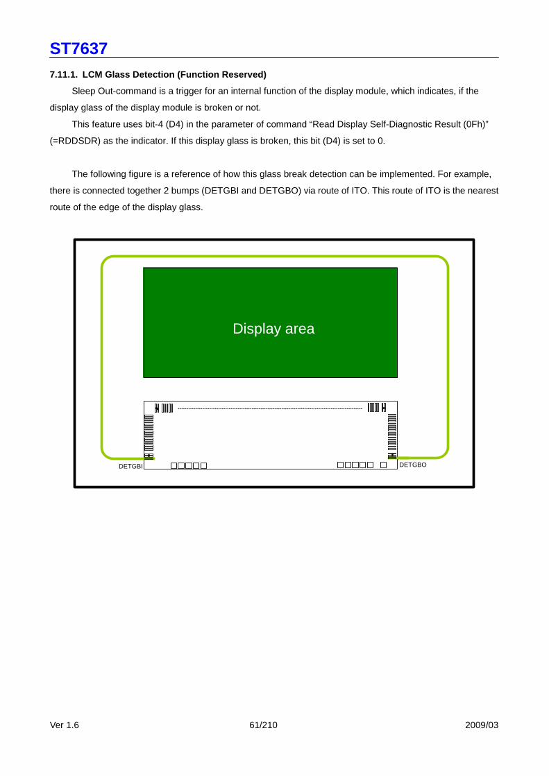
7.11.1. LCM Glass Detection (Function Reserved)
Sleep Out-command is a trigger for an internal function of the display module, which indicates, if the
display glass of the display module is broken or not.
This feature uses bit-4 (D4) in the parameter of command “Read Display Self-Diagnostic Result (0Fh)”
(=RDDSDR) as the indicator. If this display glass is broken, this bit (D4) is set to 0.
The following figure is a reference of how this glass break detection can be implemented. For example,
there is connected together 2 bumps (DETGBI and DETGBO) via route of ITO. This route of ITO is the nearest
route of the edge of the display glass.
DETGBO DETGBI
Display area

ST7637
Ver 1.6 62/210 2009/03
8. RESET CIRCUIT The registers that are initialized are listed below.
Item After Power On After Software Reset After Hardware Reset
Frame memory (RAM data) Random No Change No Change
RDDID TBD TBD TBD
RDDPM 08h 08h 08h
RDDMADCTR 00h No Change 00h
RDDCOLMOD 05h (16-Bit/Pixel) No Change 05h (16-Bit/Pixel)
RDDIM 00h 00h 00h
RDDSM 00h 00h 00h
RDDSDR 00h 00h 00h Sleep In/Out In In In
Display mode (normal/partial) Normal Normal Normal
Display Inversion On/Off Off Off Off
All Pixel Off mode Disable Disable Disable
All Pixel On mode Disable Disable Disable
Contrast (EV) 3Fh 3Fh 3Fh
Display On/Off Display Off Display Off Display Off Column: Start Address (XS) 00h 00h 00h Column: End Address (XE) 83h 83h (when MV=0)
83h (when MV=1)
83h
Row: Start Address (YS) 00h 00h 00h Row: End Address (YE) 83h 83h (when MV=0)
83h (when MV=1) 83h
Color set Random Contents of the look-up
table protected
Random
Partial: Start Address (PS) 00h 00h 00h
Partial: End Address (PE) 83h 83h 83h
Scroll: Top Fixed Area (TFA) 00h 00h 00h Scroll: Scroll Area (VSA) 84h 84h 84h Scroll: Bottom Fixed Area (BFA) 00h 00h 00h TE On/Off Off Off Off
TE Mode 0 (Mode1) 0 (Mode1) 0 (Mode1) Memory Data Access Control MY/MX/MV/ML/RGB)
0/0/0/0/0 No Change 0/0/0/0/0
Scroll Start Address (SSA) 00h 00h 00h Idle Mode On/Off Off Off Off
Interface Color Pixel Format (P) 05h (16Bit/Pixel) No change 05h (16Bit/Pixel)
ID1 Set by customer Set by customer Set by customer ID2 Set by customer Set by customer Set by customer ID3 Set by customer Set by customer Set by customer Drive Duty 83h 83h 83h
First Common 00h 00h 00h
FOSC Divider No division No division No division
ST7637
Ver 1.6 63/210 2009/03
Item After Power On After Software Reset After Hardware Reset
Vop 0D2h 0D2h 0D2h
Vop Offset increase/decrease disable disable disable
Bias 1/9 Bias 1/9 Bias 1/9 Bias
Booster setting 8x 8x 8x
Booster Efficiency 01 01 01
Vg source From 2VDD2 From 2VDD2 From 2VDD2
EPCTIN 0 0 0
OTP selection Disable Disable Disable Frame Frequency in Normal Color (FA/FB/FC/FD)
46Hz/61.5Hz/72Hz/77Hz 46Hz/61.5Hz/72Hz/77Hz 46Hz/61.5Hz/72Hz/77Hz
Frame Frequency in 8-Color (Idle) (F8A/F8B/F8C/F8D)
46Hz/61.5Hz/72Hz/77Hz 46Hz/61.5Hz/72Hz/77Hz 46Hz/61.5Hz/72Hz/77Hz
Temperature Range (TA/TB/TC)
-10 /0 /10 -10 /0 /10 -10 /0 /10
Temperature Hysteresis (TH) 6 6 6 TEMPSEL Refer to 9.1.72 Refer to 9.1.72 Refer to 9.1.72

ST7637
Ver 1.6 64/210 2009/03
9. INSTRUCTIONS 9.1 Instruction table
Command Table-1 , /EXT= H , L, or floating
Hex Command A0 /RD /WR D7 D6 D5 D4 D3 D2 D1 D0 Function Ref
(00h) NOP 0 1 0 0 0 0 0 0 0 0 0 No Operation 9.1.1
(01h) SWRESET 0 1 0 0 0 0 0 0 0 0 1 Software reset 9.1.2
(04h) RDDID 0 1 0 0 0 0 0 0 1 0 0 Read Display ID 9.1.3
- 1 0 1 - - - - - - - - Dummy read
- 1 0 1 ID17 ID16 ID15 ID14 ID13 ID12 ID11 ID10 ID1 read (D23-D16)
- 1 0 1 1 ID26 ID25 ID24 ID23 ID22 ID21 ID20 ID2 read (D15-D8)
- 1 0 1 ID37 ID36 ID35 ID34 ID33 ID32 ID31 ID30 ID3 read (D7-D0)
(09h) RDDST 0 1 0 0 0 0 0 1 0 0 1 Read Display Status 9.1.4
- 1 0 1 - - - - - - - - Dummy read
- 1 0 1 ST31 ST30 ST29 ST28 ST27 ST26 ST25 ST24 (D31-D24)
- 1 0 1 ST23 ST22 ST21 ST20 ST19 ST18 ST17 ST16 (D23-D16)
- 1 0 1 ST15 ST14 ST13 ST12 ST11 ST10 ST9 ST8 (D15-D8)
- 1 0 1 ST7 ST6 ST5 ST4 ST3 ST2 ST1 ST0 (D7-D0)
(0Ah) RDDPM 0 1 0 0 0 0 0 1 0 1 0 Read Display Power Mode 9.1.5
- 1 0 1 - - - - - - - - Dummy read
- 1 0 1 D7 D6 D5 D4 D3 D2 0 0 -
(0Bh) RDDMADCTR 0 1 0 0 0 0 0 1 0 1 1 Read Display MADCTR 9.1.6
- 1 0 1 - - - - - - - - Dummy read
- 1 0 1 D7 D6 D5 D4 D3 0 0 0 -
(0Ch) RDDCOLMOD 0 1 0 0 0 0 0 1 1 0 0 Read Display Pixel Format 9.1.7
- 1 0 1 - - - - - - - - Dummy read
- 1 0 1 0 0 0 0 0 D2 D1 D0 -
(0Dh) RDDIM 0 1 0 0 0 0 0 1 1 0 1 Read Display Image Mode 9.1.8
- 1 0 1 - - - - - - - - Dummy read
- 1 0 1 D7 0 D5 D4 D3 0 0 0 -
(0Eh) RDDSM 0 1 0 0 0 0 0 1 1 1 0 Read Display Image Mode 9.1.9
- 1 0 1 - - - - - - - - Dummy read
- 1 0 1 D7 D6 0 0 0 0 0 0 -
(0Fh) RDDSDR 0 1 0 0 0 0 0 1 1 1 1 Read Display Self-diagnostic
result 9.1.10
- 1 0 1 - - - - - - - - Dummy read
1 0 1 1 1 1 D4 0 0 0 0 -

ST7637
Ver 1.6 65/210 2009/03
(10h) SLPIN 0 1 0 0 0 0 1 0 0 0 0 Sleep in & booster off 9.1.11
(11h) SLPOUT 0 1 0 0 0 0 1 0 0 0 1 Sleep out & booster on 9.1.12
(12h) PTLON 0 1 0 0 0 0 1 0 0 1 0 Partial mode on 9.1.13
(13h) NORON 0 1 0 0 0 0 1 0 0 1 1 Partial off (Normal) 9.1.14
(20h) INVOFF 0 1 0 0 0 1 0 0 0 0 0 Display inversion off (normal) 9.1.15
(21h) INVON 0 1 0 0 0 1 0 0 0 0 1 Display inversion on 9.1.16
(22h) APOFF 0 1 0 0 0 1 0 0 0 1 0 All pixel off (Only for test
purpose)
9.1.17
(23h) APON 0 1 0 0 0 1 0 0 0 1 1 All pixel on (Only for test
purpose)
9.1.18
(25h) WRCNTR 0 1 0 0 0 1 0 0 1 0 1 Write contrast 9.1.19
- 1 1 0 0 EV6 EV5 EV4 EV3 EV2 EV1 EV0 EV = 0 to 127
(28h) DISPOFF 0 1 0 0 0 1 0 1 0 0 0 Display off 9.1.20
(29h) DISPON 0 1 0 0 0 1 0 1 0 0 1 Display on 9.1.21
(2Ah) CASET 0 1 0 0 0 1 0 1 0 1 0 Column address set 9.1.22
1 1 0 XS7 XS6 XS5 XS4 XS3 XS2 XS1 XS0 X_ADR start: 0XS83h
1 1 0 XE7 XE6 XE5 XE4 XE3 XE2 XE1 XE0 X_ADR end: XSXE 83h
(2Bh) RASET 0 1 0 0 0 1 0 1 0 1 1 Row address set 9.1.23
1 1 0 YS7 YS6 YS5 YS4 YS3 YS2 YS1 YS0 Y_ADR start: 0YS83h
1 1 0 YE7 YE6 YE5 YE4 YE3 YE2 YE1 YE0 Y_ADR end: YSYE83h
(2Ch) RAMWR 0 1 0 0 0 1 0 1 1 0 0 Memory write 9.1.24
1 1 0 D7 D6 D5 D4 D3 D2 D1 D0 Write data
(2Dh) RGBSET 0 1 0 0 0 1 0 1 1 0 1 Color set for 256 or 4k color
display 9.1.25
- 1 1 0 - - - R4 R3 R2 R1 R0 Red tone (00000)
- 1 1 0 : : : : : : : : : -
- 1 1 0 - - - R4 R3 R2 R1 R0 Red tone (11111)
- 1 1 0 - - G5 G4 G3 G2 G1 G0 Green tone (000000)
1 1 0 : : : : : : : : : -
1 1 0 - - G5 G4 G3 G2 G1 G0 Green tone (111111)
1 1 0 - - - B4 B3 B2 B1 B0 Blue tone (00000)
1 1 0 : : : : : : : : : -
1 1 0 - - - B4 B3 B2 B1 B0 Blue tone (11111)
(2Eh) RAMRD 0 1 0 0 0 1 0 1 1 1 0 Memory Read 9.1.26
1 1 0 - - - - - - - - Dummy read
1 1 0 D7 D6 D5 D4 D3 D2 D1 D0
(30h) PTLAR 0 1 0 0 0 1 1 0 0 0 0 Partial start/end address set 9.1.27
ST7637
Ver 1.6 66/210 2009/03
- 1 1 0 PS7 PS6 PS5 PS4 PS3 PS2 PS1 PS0 Start address (0~131)
- 1 1 0 PE7 PE6 PE5 PE4 PE3 PE2 PE1 PE0 End address (0~131)
(33h) SCRLAR 0 1 0 0 0 1 1 0 0 1 1 Scroll Area 9.1.28
- 1 1 0 TFA7 TFA6 TFA5 TFA4 TFA3 TFA2 TFA1 TFA0 TFA=0~132
- 1 1 0 VSA7 VSA6 VSA5 VSA4 VSA3 VSA2 VSA1 VSA0 VSA=0~132
- 1 1 0 BFA7 BFA6 BFA5 BFA4 BFA3 BFA2 BFA1 BFA0 BFA=0~132
(34h) TEOFF 0 1 0 0 0 1 1 0 1 0 0 Tearing effect line off 9.1.29
(35h) TEON 0 1 0 0 0 1 1 0 1 0 1 Tearing effect mode set & on 9.1.30
- 1 1 0 - - - - - - - M “0”: mode1, “1”: mode2
(36h) MADCTR 0 1 0 0 0 1 1 0 1 1 0 Memory data access control 9.1.31
- 1 1 0 MY MX MV ML RGB - - - -
(37h) VSCSAD 0 1 0 0 0 1 1 0 1 1 1 Scroll start address of RAM 9.1.32
1 1 0 SSA7 SSA6 SSA5 SSA4 SSA3 SSA2 SSA1 SSA0 SSA = 0~131
(38h) IDMOFF 0 1 0 0 0 1 1 1 0 0 0 Idle mode off 9.1.33
(39h) IDMON 0 1 0 0 0 1 1 1 0 0 1 Idle mode on 9.1.34
(3Ah) COLMOD 0 1 0 0 0 1 1 1 0 1 0 Interface pixel format 9.1.35
- 1 1 0 - - - - - P2 P1 P0 Interface format
(DAh) RDID1 0 1 0 1 1 0 1 1 0 1 0 Read ID1 9.1.36
- 1 0 1 - - - - - - - - Dummy read
- 1 0 1 ID17 ID16 ID15 ID14 ID13 ID12 ID11 ID10 (D7-D0)
(DBh) RDID2 0 1 0 1 1 0 1 1 0 1 1 Read ID2 9.1.37
- 1 0 1 - - - - - - - - Dummy read
- 1 0 1 ID27 ID26 ID25 ID24 ID23 ID22 ID21 ID20 (D7-D0)
(DCh) RDID3 0 1 0 1 1 0 1 1 1 0 0 Read ID3 9.1.38
- 1 0 1 - - - - - - - - Dummy read
- 1 0 1 ID37 ID36 ID35 ID34 ID33 ID32 ID31 ID30 (D7-D0)
Note 1: When /EXT connects to H or floating, commands which are not defined in “Command Table-1” are treated as NOP
(00H) command.
Note 2: Commands 10H, 12H, 13H, 20H, 21H, 25H, 28H, 29H, 30H, 36H (Bit ML only), 38H and 39H are updated during
V-sync when Module is in Sleep Out Mode to avoid abnormal visual effects.
During Sleep In mode, these commands are updated immediately.
Read status (09H), Read Display Power Mode (0AH), Read Display MADCTR (0BH), Read Display Pixel Format (0CH),
Read Display Image Mode (0DH), Read Display Signal Mode (0EH) and Read Display Self Diagnostic Result (0FH) of
these commands is updated immediately both in Sleep In mode and Sleep Out mode.

ST7637
Ver 1.6 67/210 2009/03
Command Table-2 , /EXT= L or command D7h[7] enable
Hex Command A0 /RD /WR D7 D6 D5 D4 D3 D2 D1 D0 Function Ref
(B0h) DutySet 0 1 0 1 0 1 1 0 0 0 0 Display Duty setting 9.1.39
1 1 0 Du7 Du6 Du5 Du4 Du3 Du2 Du1 Du0
(B1h) FirstCom 0 1 0 1 0 1 1 0 0 0 1 First Com. Page address 9.1.40
1 1 0 -- F6 F5 F4 F3 F2 F1 F0
(B3h) OscDiv 0 1 0 1 0 1 1 0 0 1 1 FOSC divider 9.1.41
1 1 0 - - - - - - CLD1 CLD0
(B5h) NLInvSet 0 1 0 1 0 1 1 0 1 0 1 N-line control 9.1.42
1 1 0 M N6 N5 N4 N3 N2 N1 N0
(B7h) ComScanDir 0 1 0 1 0 1 1 0 1 1 1 Com/Seg Scan Direction
for Glass layout
9.1.43
1 1 0 0 SMX 0 0 SBGR 0 - -
(B8h) RmwIn 0 1 0 1 0 1 1 1 0 0 0 read modify write control
IN
9.1.44
(B9h) RmwOut 0 1 0 1 0 1 1 1 0 0 1 read modify write control
Out
9.1.45
(C0h) VopSet 0 1 0 1 1 0 0 0 0 0 0 Vop setting 9.1.46
1 1 0 Vop7 Vop6 Vop5 Vop4 Vop3 Vop2 Vop1 Vop0
1 1 0 - - - - - - - Vop8
(C1h) VopOfsetInc 0 1 0 1 1 0 0 0 0 0 1 +40mv/setp 9.1.47
(C2h) VopOfsetDec 0 1 0 1 1 0 0 0 0 1 0 -40mv/setp 9.1.48
(C3h) BiasSel 0 1 0 1 1 0 0 0 0 1 1 Bias selection 9.1.49
1 1 0 - - - - - Bias2 Bias1 Bias0
(C4h) BstBmpXSel 0 1 0 1 1 0 0 0 1 0 0 Booster setting 9.1.50
1 1 0 - - - - - BST2 BST 1 BST0
(C5h) BstEffSel 0 1 0 1 1 0 0 0 1 0 1 Booster efficiency
selection
9.1.51
1 1 0 - - - - - - BTF1 BTF0
(C7h) VopOffset 0 1 0 1 1 0 0 0 1 1 1 9.1.52
1 1 0 VOS7 VOS6 VOS5 VOS4 VOS3 VOS2 VOS1 VOS0
1 1 0 - - - - - - - VOS8
(CBh) VgSorcSel 0 1 0 1 1 0 0 1 0 1 1 FV3 with Booster x2 control 9.1.53
1 1 0 - - - - - - - 2BT0
(CCh) ID1Set 0 1 0 1 1 0 0 1 1 0 0 ID1 setting 9.1.54
1 1 0 ID1_7 ID1_6 ID1_5 ID1_4 ID1_3 ID1_2 ID1_1 ID1_0
(CDh) ID2Set 0 1 0 1 1 0 0 1 1 0 1 ID2 setting 9.1.55
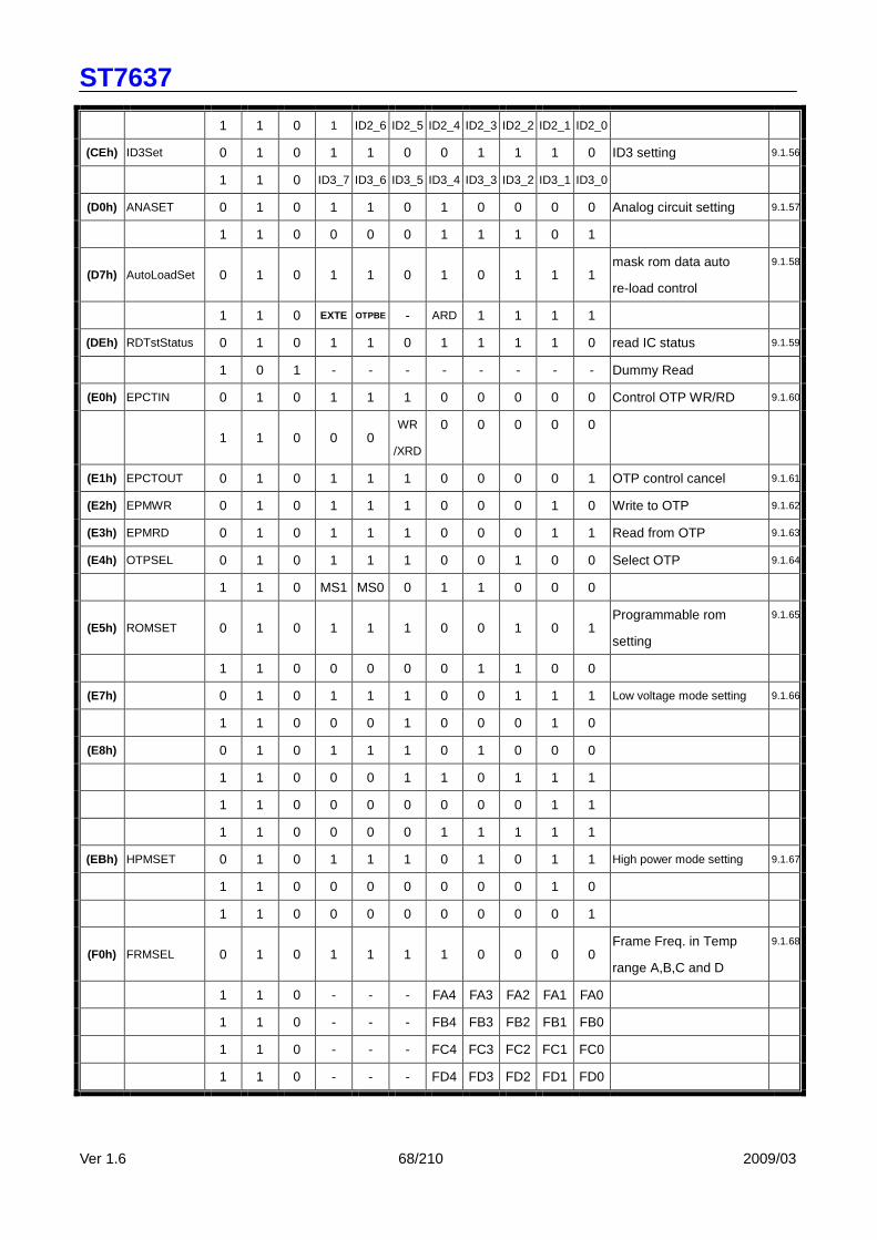
ST7637
Ver 1.6 68/210 2009/03
1 1 0 1 ID2_6 ID2_5 ID2_4 ID2_3 ID2_2 ID2_1 ID2_0
(CEh) ID3Set 0 1 0 1 1 0 0 1 1 1 0 ID3 setting 9.1.56
1 1 0 ID3_7 ID3_6 ID3_5 ID3_4 ID3_3 ID3_2 ID3_1 ID3_0
(D0h) ANASET 0 1 0 1 1 0 1 0 0 0 0 Analog circuit setting 9.1.57
1 1 0 0 0 0 1 1 1 0 1
(D7h) AutoLoadSet 0 1 0 1 1 0 1 0 1 1 1 mask rom data auto
re-load control
9.1.58
1 1 0 EXTE OTPBE - ARD 1 1 1 1
(DEh) RDTstStatus 0 1 0 1 1 0 1 1 1 1 0 read IC status 9.1.59
1 0 1 - - - - - - - - Dummy Read
(E0h) EPCTIN 0 1 0 1 1 1 0 0 0 0 0 Control OTP WR/RD 9.1.60
1 1 0 0 0 WR
/XRD
0 0 0 0 0
(E1h) EPCTOUT 0 1 0 1 1 1 0 0 0 0 1 OTP control cancel 9.1.61
(E2h) EPMWR 0 1 0 1 1 1 0 0 0 1 0 Write to OTP 9.1.62
(E3h) EPMRD 0 1 0 1 1 1 0 0 0 1 1 Read from OTP 9.1.63
(E4h) OTPSEL 0 1 0 1 1 1 0 0 1 0 0 Select OTP 9.1.64
1 1 0 MS1 MS0 0 1 1 0 0 0
(E5h) ROMSET 0 1 0 1 1 1 0 0 1 0 1 Programmable rom
setting
9.1.65
1 1 0 0 0 0 0 1 1 0 0
(E7h) 0 1 0 1 1 1 0 0 1 1 1 Low voltage mode setting 9.1.66
1 1 0 0 0 1 0 0 0 1 0
(E8h) 0 1 0 1 1 1 0 1 0 0 0
1 1 0 0 0 1 1 0 1 1 1
1 1 0 0 0 0 0 0 0 1 1
1 1 0 0 0 0 1 1 1 1 1
(EBh) HPMSET 0 1 0 1 1 1 0 1 0 1 1 High power mode setting 9.1.67
1 1 0 0 0 0 0 0 0 1 0
1 1 0 0 0 0 0 0 0 0 1
(F0h) FRMSEL 0 1 0 1 1 1 1 0 0 0 0 Frame Freq. in Temp
range A,B,C and D
9.1.68
1 1 0 - - - FA4 FA3 FA2 FA1 FA0
1 1 0 - - - FB4 FB3 FB2 FB1 FB0
1 1 0 - - - FC4 FC3 FC2 FC1 FC0
1 1 0 - - - FD4 FD3 FD2 FD1 FD0
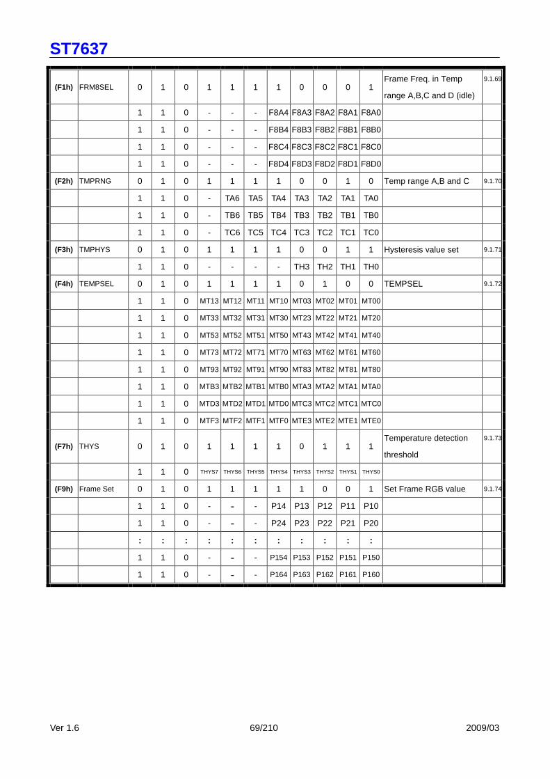
ST7637
Ver 1.6 69/210 2009/03
(F1h) FRM8SEL 0 1 0 1 1 1 1 0 0 0 1 Frame Freq. in Temp
range A,B,C and D (idle)
9.1.69
1 1 0 - - - F8A4 F8A3 F8A2 F8A1 F8A0
1 1 0 - - - F8B4 F8B3 F8B2 F8B1 F8B0
1 1 0 - - - F8C4 F8C3 F8C2 F8C1 F8C0
1 1 0 - - - F8D4 F8D3 F8D2 F8D1 F8D0
(F2h) TMPRNG 0 1 0 1 1 1 1 0 0 1 0 Temp range A,B and C 9.1.70
1 1 0 - TA6 TA5 TA4 TA3 TA2 TA1 TA0
1 1 0 - TB6 TB5 TB4 TB3 TB2 TB1 TB0
1 1 0 - TC6 TC5 TC4 TC3 TC2 TC1 TC0
(F3h) TMPHYS 0 1 0 1 1 1 1 0 0 1 1 Hysteresis value set 9.1.71
1 1 0 - - - - TH3 TH2 TH1 TH0
(F4h) TEMPSEL 0 1 0 1 1 1 1 0 1 0 0 TEMPSEL 9.1.72
1 1 0 MT13 MT12 MT11 MT10 MT03 MT02 MT01 MT00
1 1 0 MT33 MT32 MT31 MT30 MT23 MT22 MT21 MT20
1 1 0 MT53 MT52 MT51 MT50 MT43 MT42 MT41 MT40
1 1 0 MT73 MT72 MT71 MT70 MT63 MT62 MT61 MT60
1 1 0 MT93 MT92 MT91 MT90 MT83 MT82 MT81 MT80
1 1 0 MTB3 MTB2 MTB1 MTB0 MTA3 MTA2 MTA1 MTA0
1 1 0 MTD3 MTD2 MTD1 MTD0 MTC3 MTC2 MTC1 MTC0
1 1 0 MTF3 MTF2 MTF1 MTF0 MTE3 MTE2 MTE1 MTE0
(F7h) THYS 0 1 0 1 1 1 1 0 1 1 1 Temperature detection
threshold
9.1.73
1 1 0 THYS7 THYS6 THYS5 THYS4 THYS3 THYS2 THYS1 THYS0
(F9h) Frame Set 0 1 0 1 1 1 1 1 0 0 1 Set Frame RGB value 9.1.74
1 1 0 - - - P14 P13 P12 P11 P10
1 1 0 - - - P24 P23 P22 P21 P20
: : : : : : : : : : :
1 1 0 - - - P154 P153 P152 P151 P150
1 1 0 - - - P164 P163 P162 P161 P160
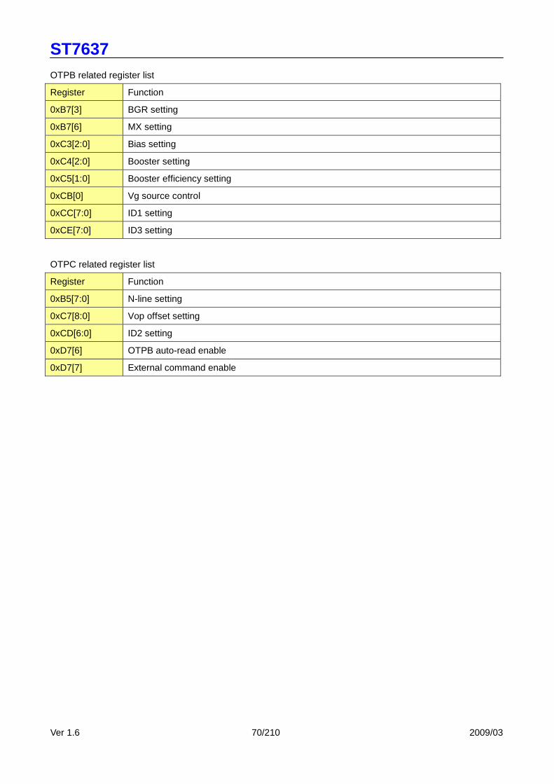
ST7637
Ver 1.6 70/210 2009/03
OTPB related register list
Register Function
0xB7[3] BGR setting
0xB7[6] MX setting
0xC3[2:0] Bias setting
0xC4[2:0] Booster setting
0xC5[1:0] Booster efficiency setting
0xCB[0] Vg source control
0xCC[7:0] ID1 setting
0xCE[7:0] ID3 setting
OTPC related register list
Register Function
0xB5[7:0] N-line setting
0xC7[8:0] Vop offset setting
0xCD[6:0] ID2 setting
0xD7[6] OTPB auto-read enable
0xD7[7] External command enable
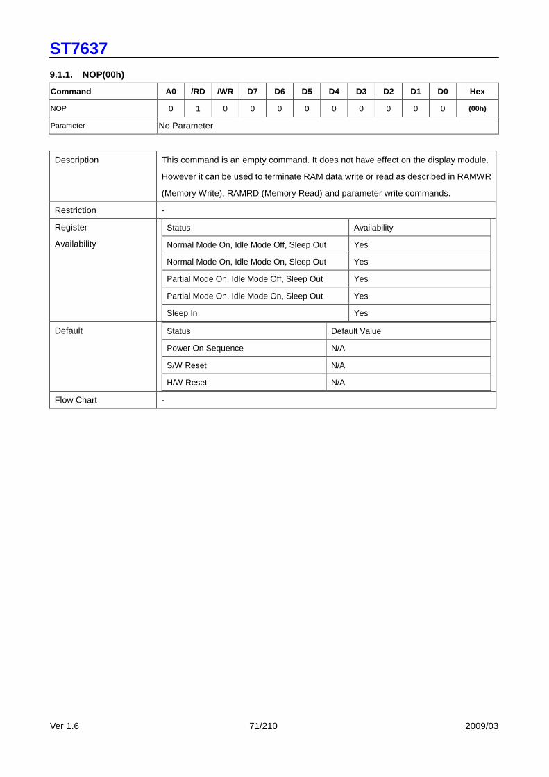
ST7637
Ver 1.6 71/210 2009/03
9.1.1. NOP(00h)
Command A0 /RD /WR D7 D6 D5 D4 D3 D2 D1 D0 Hex
NOP 0 1 0 0 0 0 0 0 0 0 0 (00h)
Parameter No Parameter
Description This command is an empty command. It does not have effect on the display module.
However it can be used to terminate RAM data write or read as described in RAMWR
(Memory Write), RAMRD (Memory Read) and parameter write commands.
Restriction -
Register
Availability
Status Availability
Normal Mode On, Idle Mode Off, Sleep Out Yes
Normal Mode On, Idle Mode On, Sleep Out Yes
Partial Mode On, Idle Mode Off, Sleep Out Yes
Partial Mode On, Idle Mode On, Sleep Out Yes
Sleep In Yes Default Status Default Value
Power On Sequence N/A
S/W Reset N/A
H/W Reset N/A Flow Chart -

ST7637
Ver 1.6 72/210 2009/03
9.1.2. SWRESET: Software Reset (01h)
Command A0 /RD /WR D7 D6 D5 D4 D3 D2 D1 D0 Hex
SWRESET 0 1 0 0 0 0 0 0 0 0 1 (01h)
Parameter No Parameter
Description When the Software Reset command is written, it causes a software reset. It resets the
commands and parameters to their S/W Reset default values and all segment &
common outputs are set to Vm (display off: blank display). (See default tables in each
command description)
Note: The Frame Memory contents are not affected by this command.
Restriction It will be necessary to wait 5msec before sending new command following software
reset. The display module loads all display suppliers’ factory default values to the
registers during 5msec. If Software Reset is applied during Sleep Out mode, it will be
necessary to wait 120msec before sending Sleep Out command.
Software Reset command cannot be sent during Sleep Out sequence.
Register
Availability
Status Availability
Normal Mode On, Idle Mode Off, Sleep Out Yes
Normal Mode On, Idle Mode On, Sleep Out Yes
Partial Mode On, Idle Mode Off, Sleep Out Yes
Partial Mode On, Idle Mode On, Sleep Out Yes
Sleep In Yes Default Status Default Value
Power On Sequence N/A
S/W Reset N/A
H/W Reset N/A Flow Chart
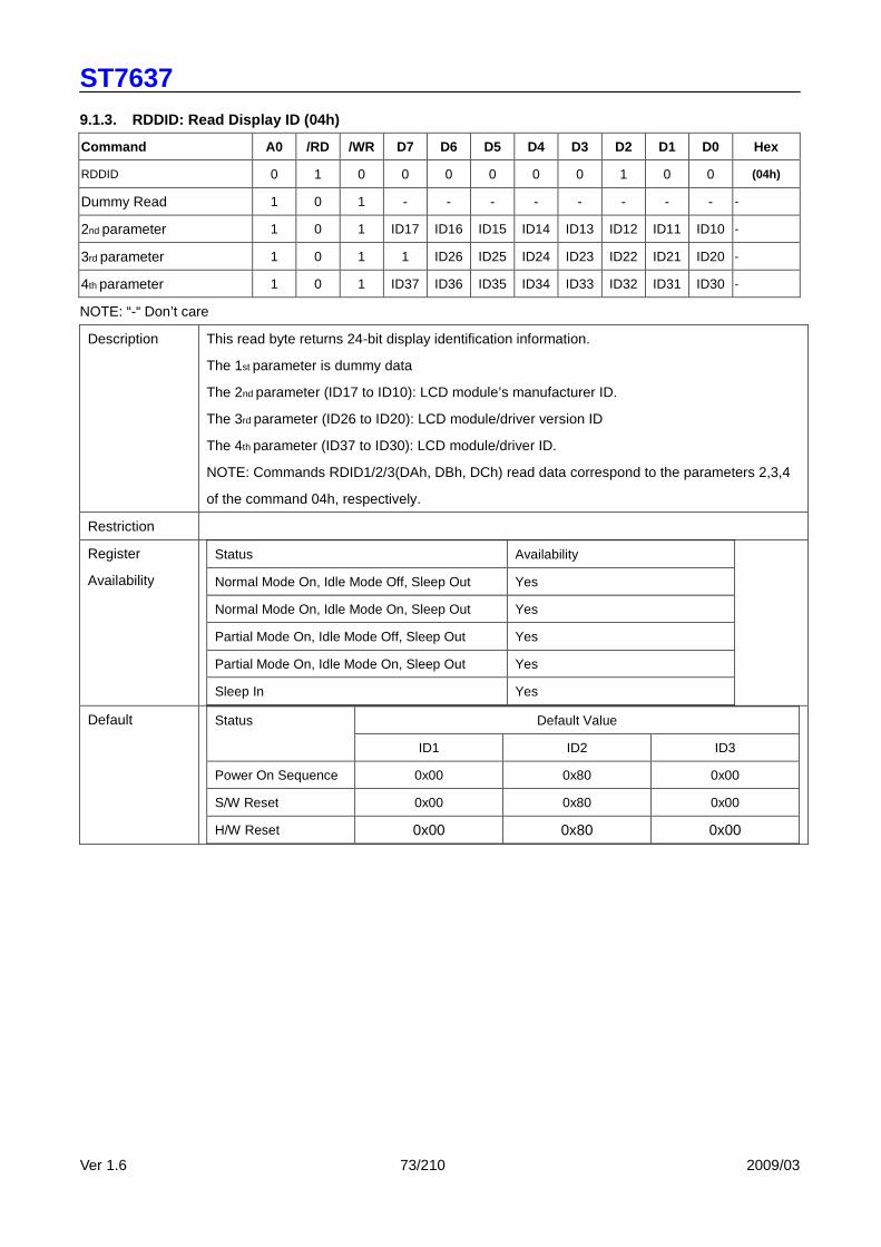
ST7637
Ver 1.6 73/210 2009/03
9.1.3. RDDID: Read Display ID (04h)
Command A0 /RD /WR D7 D6 D5 D4 D3 D2 D1 D0 Hex
RDDID 0 1 0 0 0 0 0 0 1 0 0 (04h)
Dummy Read 1 0 1 - - - - - - - - -
2nd parameter 1 0 1 ID17 ID16 ID15 ID14 ID13 ID12 ID11 ID10 -
3rd parameter 1 0 1 1 ID26 ID25 ID24 ID23 ID22 ID21 ID20 -
4th parameter 1 0 1 ID37 ID36 ID35 ID34 ID33 ID32 ID31 ID30 -
NOTE: “-“ Don’t care
Description This read byte returns 24-bit display identification information.
The 1st parameter is dummy data
The 2nd parameter (ID17 to ID10): LCD module’s manufacturer ID.
The 3rd parameter (ID26 to ID20): LCD module/driver version ID
The 4th parameter (ID37 to ID30): LCD module/driver ID.
NOTE: Commands RDID1/2/3(DAh, DBh, DCh) read data correspond to the parameters 2,3,4
of the command 04h, respectively.
Restriction
Register
Availability
Status Availability
Normal Mode On, Idle Mode Off, Sleep Out Yes
Normal Mode On, Idle Mode On, Sleep Out Yes
Partial Mode On, Idle Mode Off, Sleep Out Yes
Partial Mode On, Idle Mode On, Sleep Out Yes
Sleep In Yes Default Default Value Status
ID1 ID2 ID3
Power On Sequence 0x00 0x80 0x00
S/W Reset 0x00 0x80 0x00
H/W Reset 0x00 0x80 0x00
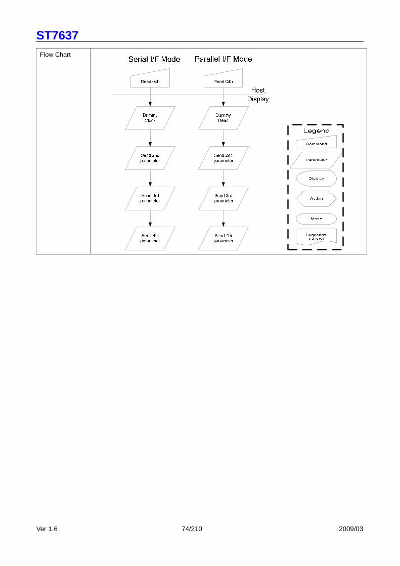
ST7637
Ver 1.6 74/210 2009/03
Flow Chart

ST7637
Ver 1.6 75/210 2009/03
9.1.4. RDDST: Read Display Status (09h)
Command A0 /RD /WR D7 D6 D5 D4 D3 D2 D1 D0 Hex
RDDST 0 1 0 0 0 0 0 1 0 0 1 (09h)
Dummy Read 1 0 1 - - - - - - - - -
2nd parameter 1 0 1 ST31 ST30 ST29 ST28 ST27 ST26 ST25 ST24 -
3rd parameter 1 0 1 ST23 ST22 ST21 ST20 ST19 ST18 ST17 ST16 -
4th parameter 1 0 1 ST15 ST14 ST13 ST12 ST11 ST10 ST9 ST8 -
5th parameter 1 0 1 ST7 ST6 ST5 ST4 ST3 ST2 ST1 ST0 -
NOTE: “-“ Don’t care
Description This command indicates the current status of the display as described in the table below:
Bit Description Value
ST31 Booster Voltage Status “1”=Booster on, “0”=off
ST30 Row Address Order (MY) “1”=Decrement, “0”=Increment
ST29 Column Address Order (MX) “1”=Decrement, “0”=Increment
ST28 Row/Column Order (MV) “1”= Row/column exchange (MV=1)
“0”= Normal (MV=0)
ST27 Scan Address Order (ML) “1”=Decrement, “0”=Increment
ST26 RGB/BGR Order (RGB) “1”=BGR, “0”=RGB
ST25 Not Used “0”
ST24 Not Used “0”
ST23 Not Used “0” ST22
ST21
ST20
Interface Color Pixel Format Definition
“010” = 8-bit / pixel, “011” = 12-bit / pixel type A “100” = 12-bit / pixel type B “101” = 16-bit / pixel, “110” = 18-bit / pixel, “111” = 24-bit / pixel
ST19 Idle Mode On/Off “1” = On, “0” = Off
ST18 Partial Mode On/Off “1” = On, “0” = Off
ST17 Sleep In/Out “1” = Out, “0” = In
ST16 Display Normal Mode On/Off “1” = Normal Display, “0” = Partial Display
ST15 Vertical Scrolling Status “1” = Scroll on, “0” = Scroll off
ST14 Not Used “0”
ST13 Inversion Status “1” = On, “0” = Off
ST12 All Pixels On “1” = all pixal on, “0” = normal display
ST11 All Pixels Off “1” = all pixal off, “0” = normal display
ST10 Display On/Off “1” = On, “0” = Off
ST9 Tearing effect line on/off “1” = On, “0” = Off
ST8 Not Used “0”
ST7 Not Used “0”
ST6 Not Used “0”
ST5 Tearing effect line mode “0” = mode1, “1” = mode2
ST4 Not Used “0”
ST3 Not Used “0”
ST2 Not Used “0”
ST1 Not Used “0”
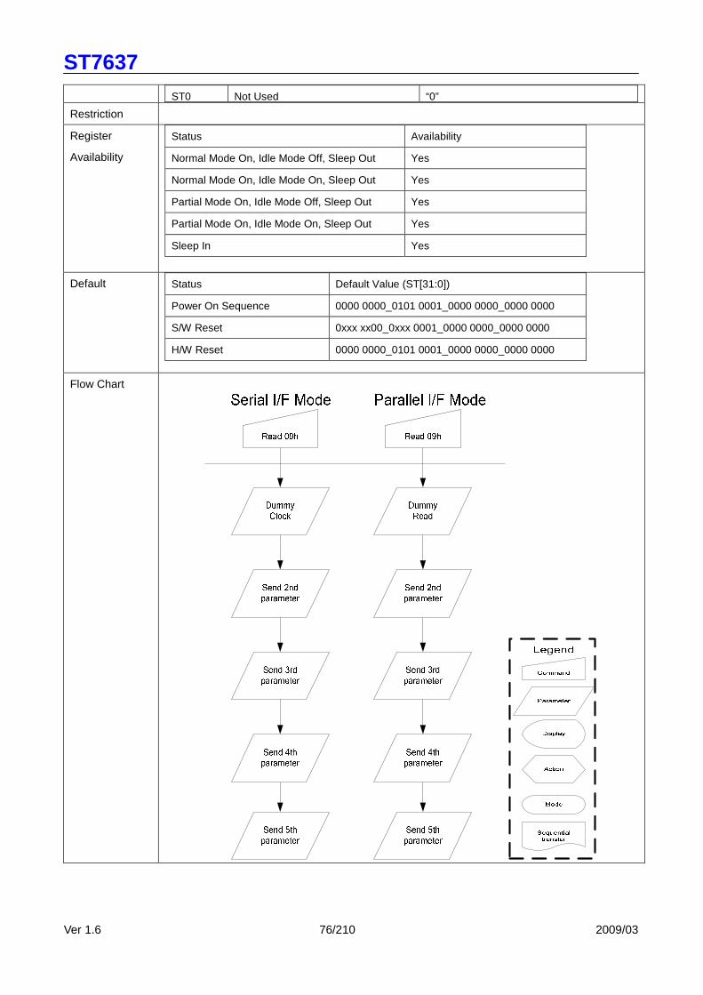
ST7637
Ver 1.6 76/210 2009/03
ST0 Not Used “0” Restriction
Register
Availability
Status Availability
Normal Mode On, Idle Mode Off, Sleep Out Yes
Normal Mode On, Idle Mode On, Sleep Out Yes
Partial Mode On, Idle Mode Off, Sleep Out Yes
Partial Mode On, Idle Mode On, Sleep Out Yes
Sleep In Yes
Default
Status Default Value (ST[31:0])
Power On Sequence 0000 0000_0101 0001_0000 0000_0000 0000
S/W Reset 0xxx xx00_0xxx 0001_0000 0000_0000 0000
H/W Reset 0000 0000_0101 0001_0000 0000_0000 0000
Flow Chart
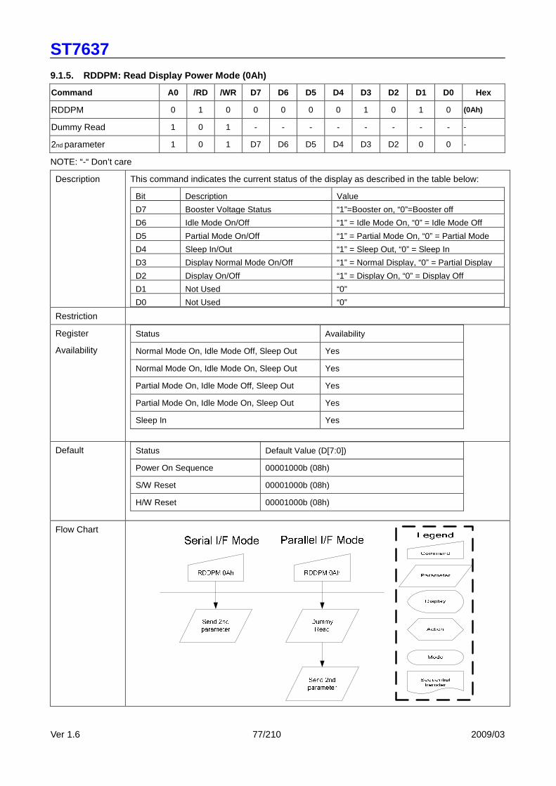
ST7637
Ver 1.6 77/210 2009/03
9.1.5. RDDPM: Read Display Power Mode (0Ah)
Command A0 /RD /WR D7 D6 D5 D4 D3 D2 D1 D0 Hex
RDDPM 0 1 0 0 0 0 0 1 0 1 0 (0Ah)
Dummy Read 1 0 1 - - - - - - - - -
2nd parameter 1 0 1 D7 D6 D5 D4 D3 D2 0 0 -
NOTE: “-“ Don’t care
Description This command indicates the current status of the display as described in the table below:
Bit Description Value
D7 Booster Voltage Status “1”=Booster on, “0”=Booster off
D6 Idle Mode On/Off “1” = Idle Mode On, “0” = Idle Mode Off
D5 Partial Mode On/Off “1” = Partial Mode On, “0” = Partial Mode
D4 Sleep In/Out “1” = Sleep Out, “0” = Sleep In
D3 Display Normal Mode On/Off “1” = Normal Display, “0” = Partial Display
D2 Display On/Off “1” = Display On, “0” = Display Off
D1 Not Used “0”
D0 Not Used “0” Restriction
Register
Availability
Status Availability
Normal Mode On, Idle Mode Off, Sleep Out Yes
Normal Mode On, Idle Mode On, Sleep Out Yes
Partial Mode On, Idle Mode Off, Sleep Out Yes
Partial Mode On, Idle Mode On, Sleep Out Yes
Sleep In Yes
Default
Status Default Value (D[7:0])
Power On Sequence 00001000b (08h)
S/W Reset 00001000b (08h)
H/W Reset 00001000b (08h)
Flow Chart
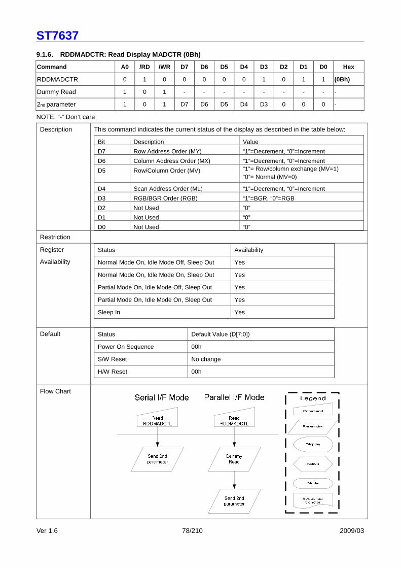
ST7637
Ver 1.6 78/210 2009/03
9.1.6. RDDMADCTR: Read Display MADCTR (0Bh)
Command A0 /RD /WR D7 D6 D5 D4 D3 D2 D1 D0 Hex
RDDMADCTR 0 1 0 0 0 0 0 1 0 1 1 (0Bh)
Dummy Read 1 0 1 - - - - - - - - -
2nd parameter 1 0 1 D7 D6 D5 D4 D3 0 0 0 -
NOTE: “-“ Don’t care
Description This command indicates the current status of the display as described in the table below:
Bit Description Value
D7 Row Address Order (MY) “1”=Decrement, “0”=Increment
D6 Column Address Order (MX) “1”=Decrement, “0”=Increment D5 Row/Column Order (MV) “1”= Row/column exchange (MV=1)
“0”= Normal (MV=0)
D4 Scan Address Order (ML) “1”=Decrement, “0”=Increment
D3 RGB/BGR Order (RGB) “1”=BGR, “0”=RGB
D2 Not Used “0”
D1 Not Used “0”
D0 Not Used “0” Restriction
Register
Availability
Status Availability
Normal Mode On, Idle Mode Off, Sleep Out Yes
Normal Mode On, Idle Mode On, Sleep Out Yes
Partial Mode On, Idle Mode Off, Sleep Out Yes
Partial Mode On, Idle Mode On, Sleep Out Yes
Sleep In Yes
Default
Status Default Value (D[7:0])
Power On Sequence 00h
S/W Reset No change
H/W Reset 00h
Flow Chart

ST7637
Ver 1.6 79/210 2009/03
9.1.7. RDDCOLMOD: Read Display Pixel Format (0Ch)
Command A0 /RD /WR D7 D6 D5 D4 D3 D2 D1 D0 Hex
RDDCOLMOD 0 1 0 0 0 0 0 1 1 0 0 (0Ch)
Dummy Read 1 0 1 - - - - - - - - -
2nd parameter 1 0 1 0 0 0 0 0 D2 D1 D0 -
NOTE: “-“ Don’t care
Description This command indicates the current status of the display as described in the table below:
Bit Description Value
D7 “0” (Not Used)
D6 “0” (Not Used)
D5 “0” (Not Used)
D4
RGB Interface Color Format
“0” (Not Used)
D3 “0” D2
D1
D0
Control Interface Color Format
“010”=8 bit/pixel “011”=12 bit/pixel (type A) “100”=12 bit/pixel (type B) “101”=16 bit/pixel "110" = 18-bit/pixel "111" = 24-bit/pixel The others = not defined
Restriction
Register
Availability
Status Availability
Normal Mode On, Idle Mode Off, Sleep Out Yes
Normal Mode On, Idle Mode On, Sleep Out Yes
Partial Mode On, Idle Mode Off, Sleep Out Yes
Partial Mode On, Idle Mode On, Sleep Out Yes
Sleep In Yes
Default
Status Default Value (D[7:0])
Power On Sequence 16 bit/pixel
S/W Reset No change
H/W Reset 16 bit/pixel

ST7637
Ver 1.6 80/210 2009/03
Flow Chart

ST7637
Ver 1.6 81/210 2009/03
9.1.8. RDDIM: Read Display Image Mode (0Dh)
Command A0 /RD /WR D7 D6 D5 D4 D3 D2 D1 D0 Hex
RDDIM 0 1 0 0 0 0 0 1 1 0 1 (0Dh)
Dummy Read 1 0 1 - - - - - - - - -
2nd parameter 1 0 1 D7 0 D5 D4 D3 0 0 0 -
NOTE: “-“ Don’t care
Description This command indicates the current status of the display as described in the table below:
Bit Description Value
D7 Vertical Scrolling On/Off “1” = Vertical scrolling is On, “0” = Vertical scrolling is Off,
D6 Not Used “0”
D5 Inversion On/Off “1” = Inversion is On, “0” = Inversion is Off
D4 All Pixels On “1” = All Pixels On, “0” = Normal Mode
D3 All Pixels Off “1” = All Pixels Off, “0” = Normal Mode D2
D1
D0
Not Used “0” “0” “0”
Restriction
Register
Availability
Status Availability
Normal Mode On, Idle Mode Off, Sleep Out Yes
Normal Mode On, Idle Mode On, Sleep Out Yes
Partial Mode On, Idle Mode Off, Sleep Out Yes
Partial Mode On, Idle Mode On, Sleep Out Yes
Sleep In Yes
Default
Status Default Value (D[7:0])
Power On Sequence 00h
S/W Reset 00h
H/W Reset 00h
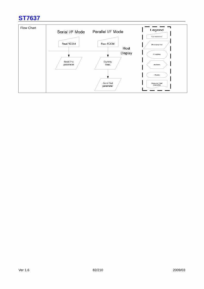
ST7637
Ver 1.6 82/210 2009/03
Flow Chart

ST7637
Ver 1.6 83/210 2009/03
9.1.9. RDDSM: Read Display Signal Mode (0Eh)
Command A0 /RD /WR D7 D6 D5 D4 D3 D2 D1 D0 Hex
RDDSM 0 1 0 0 0 0 0 1 1 1 0 (0Eh)
Dummy Read 1 0 1 - - - - - - - - -
2nd parameter 1 0 1 D7 D6 0 0 0 0 0 0 -
NOTE: “-“ Don’t care
Description This command indicates the current status of the display as described in the table below:
Bit Description Value
D7 Tearing Effect Line On/Off “1” = On, “0” = Off
D6 Tearing effect line mode “0” = mode1, “1” = mode2
D5 Not Used “0”
D4 Not Used “0”
D3 Not Used “0”
D2 Not Used “0”
D1 Not Used “0”
D0 Not Used “0” Restriction
Register
Availability
Status Availability
Normal Mode On, Idle Mode Off, Sleep Out Yes
Normal Mode On, Idle Mode On, Sleep Out Yes
Partial Mode On, Idle Mode Off, Sleep Out Yes
Partial Mode On, Idle Mode On, Sleep Out Yes
Sleep In Yes
Default
Status Default Value (D[7:0])
Power On Sequence 00h
S/W Reset 00h
H/W Reset 00h
Flow Chart

ST7637
Ver 1.6 84/210 2009/03
9.1.10. RDDSDR: Read Display Self-Diagnostic Result (0Fh)
Command A0 /RD /WR D7 D6 D5 D4 D3 D2 D1 D0 Hex
RDDSDR 0 1 0 0 0 0 0 1 1 1 1 (0Fh)
Dummy Read 1 0 1 - - - - - - - - -
2nd parameter 1 0 1 1 1 1 D4 0 0 0 0
NOTE: “-“ Don’t care
Description This command indicates the current status of the display as described in the table below:
Bit Description Value
D7 Not Used “1”
D6 Not Used “1”
D5 Not Used “1”
D4 Glass broken Detection See section7.11.1
D3 Not Used “0”
D2 Not Used “0”
D1 Not Used “0”
D0 Not Used “0” Restriction
Register
Availability
Status Availability
Normal Mode On, Idle Mode Off, Sleep Out Yes
Normal Mode On, Idle Mode On, Sleep Out Yes
Partial Mode On, Idle Mode Off, Sleep Out Yes
Partial Mode On, Idle Mode On, Sleep Out Yes
Sleep In Yes
Default
Status Default Value (D[7:0])
Power On Sequence E0h
S/W Reset E0h
H/W Reset E0h
Flow Chart
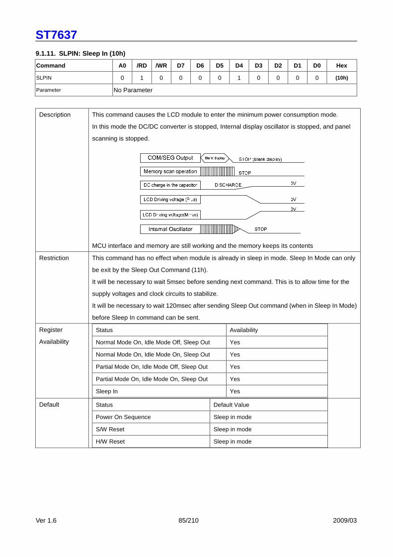
ST7637
Ver 1.6 85/210 2009/03
9.1.11. SLPIN: Sleep In (10h)
Command A0 /RD /WR D7 D6 D5 D4 D3 D2 D1 D0 Hex
SLPIN 0 1 0 0 0 0 1 0 0 0 0 (10h)
Parameter No Parameter
Description This command causes the LCD module to enter the minimum power consumption mode.
In this mode the DC/DC converter is stopped, Internal display oscillator is stopped, and panel
scanning is stopped.
MCU interface and memory are still working and the memory keeps its contents
Restriction This command has no effect when module is already in sleep in mode. Sleep In Mode can only
be exit by the Sleep Out Command (11h).
It will be necessary to wait 5msec before sending next command. This is to allow time for the
supply voltages and clock circuits to stabilize.
It will be necessary to wait 120msec after sending Sleep Out command (when in Sleep In Mode)
before Sleep In command can be sent.
Register
Availability
Status Availability
Normal Mode On, Idle Mode Off, Sleep Out Yes
Normal Mode On, Idle Mode On, Sleep Out Yes
Partial Mode On, Idle Mode Off, Sleep Out Yes
Partial Mode On, Idle Mode On, Sleep Out Yes
Sleep In Yes Default Status Default Value
Power On Sequence Sleep in mode
S/W Reset Sleep in mode
H/W Reset Sleep in mode

ST7637
Ver 1.6 86/210 2009/03
Flow Chart It takes about 120m sec to get into Sleep In mode (booster off state) after SLPIN command
issued. The results of booster off can be check by RDDST (09h) command Bit31.

ST7637
Ver 1.6 87/210 2009/03
9.1.12. SLPOUT: Sleep Out (11h)
Command A0 /RD /WR D7 D6 D5 D4 D3 D2 D1 D0 Hex
SLPOUT 0 1 0 0 0 0 1 0 0 0 1 (11h)
Parameter No Parameter
Description This command turns off sleep mode. In this mode the DC/DC converter is enabled, Internal
display oscillator is started, and panel scanning is started.
Restriction This command has no effect when module is already in sleep out mode. Sleep Out Mode can
only be exit by the Sleep In Command (10h).
It will be necessary to wait 5msec before sending next command. This is to allow time for the
supply voltages and clock circuits to stabilize.
The display module loads all display supplier’s factory default values to the registers during this
5msec and there cannot be any abnormal visual effect on the display image if factory default
and register values are same when this load is done and when the display module is already
Sleep Out –mode.
The display module is doing self-diagnostic functions during this 5msec. It will be necessary to
wait 120msec after sending Sleep In command (when in Sleep Out mode) before Sleep Out
command can be sent.
Register
Availability
Status Availability
Normal Mode On, Idle Mode Off, Sleep Out Yes
Normal Mode On, Idle Mode On, Sleep Out Yes
Partial Mode On, Idle Mode Off, Sleep Out Yes
Partial Mode On, Idle Mode On, Sleep Out Yes
Sleep In Yes Default Status Default Value
Power On Sequence Sleep in mode
S/W Reset Sleep in mode
H/W Reset Sleep in mode
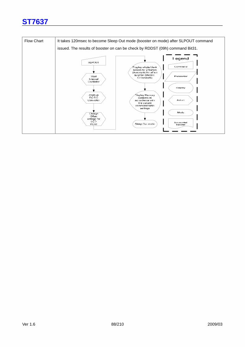
ST7637
Ver 1.6 88/210 2009/03
Flow Chart It takes 120msec to become Sleep Out mode (booster on mode) after SLPOUT command
issued. The results of booster on can be check by RDDST (09h) command Bit31.

ST7637
Ver 1.6 89/210 2009/03
9.1.13. PTLON: Partial Display Mode On (12h)
Command A0 /RD /WR D7 D6 D5 D4 D3 D2 D1 D0 Hex
PTLON 0 1 0 0 0 0 1 0 0 1 0 (12h)
Parameter No Parameter
Description This command turns on Partial mode. The partial mode window is described by the Partial Area
command (30H)
Exit from PTLON by Normal Display Mode On command (13H)
There is no abnormal visual effect during mode change between Normal mode On <-> Partial
mode On.
Restriction This command has no effect when Partial mode is active.
Register
Availability
Status Availability
Normal Mode On, Idle Mode Off, Sleep Out Yes
Normal Mode On, Idle Mode On, Sleep Out Yes
Partial Mode On, Idle Mode Off, Sleep Out Yes
Partial Mode On, Idle Mode On, Sleep Out Yes
Sleep In Yes Default Status Default Value
Power On Sequence Partial mode off
S/W Reset Partial mode off
H/W Reset Partial mode off Flow Chart See Partial Area (30h)
ST7637
Ver 1.6 90/210 2009/03
9.1.14. NORON: Normal Display Mode On (13h)
Command A0 /RD /WR D7 D6 D5 D4 D3 D2 D1 D0 Hex
NORON 0 1 0 0 0 0 1 0 0 1 1 (13h)
Parameter No Parameter
Description This command returns the display to normal mode.
Normal display mode on means Partial mode off, Scroll mode Off.
Exit from NORON by the Partial mode On command (12h)
There is no abnormal visual effect during mode change between Normal mode On <-> Partial
mode On.
Restriction This command has no effect when Normal Display mode is active.
Register
Availability
Status Availability
Normal Mode On, Idle Mode Off, Sleep Out Yes
Normal Mode On, Idle Mode On, Sleep Out Yes
Partial Mode On, Idle Mode Off, Sleep Out Yes
Partial Mode On, Idle Mode On, Sleep Out Yes
Sleep In Yes Default Status Default Value
Power On Sequence Normal Mode On
S/W Reset Normal Mode On
H/W Reset Normal Mode On Flow Chart See Partial Area and Vertical Scrolling Definition Descriptions for details of when to use this
command
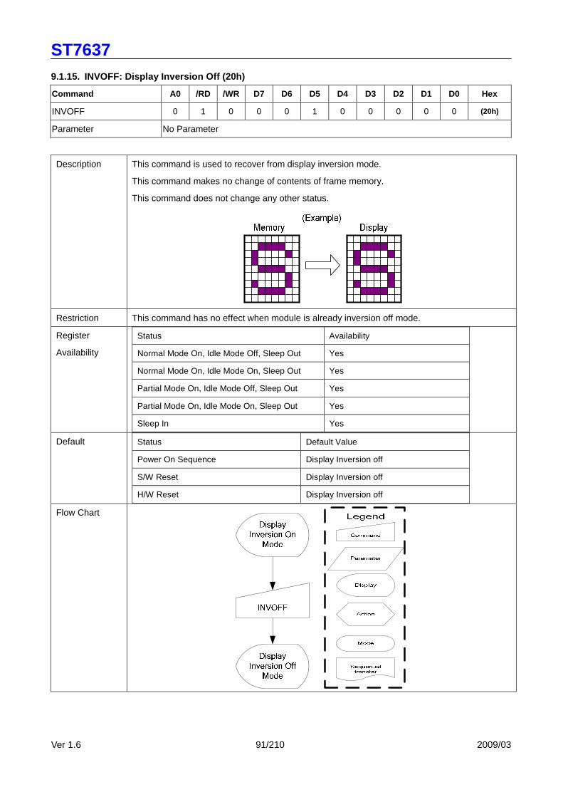
ST7637
Ver 1.6 91/210 2009/03
9.1.15. INVOFF: Display Inversion Off (20h)
Command A0 /RD /WR D7 D6 D5 D4 D3 D2 D1 D0 Hex
INVOFF 0 1 0 0 0 1 0 0 0 0 0 (20h)
Parameter No Parameter
Description This command is used to recover from display inversion mode.
This command makes no change of contents of frame memory.
This command does not change any other status.
Restriction This command has no effect when module is already inversion off mode.
Register
Availability
Status Availability
Normal Mode On, Idle Mode Off, Sleep Out Yes
Normal Mode On, Idle Mode On, Sleep Out Yes
Partial Mode On, Idle Mode Off, Sleep Out Yes
Partial Mode On, Idle Mode On, Sleep Out Yes
Sleep In Yes Default Status Default Value
Power On Sequence Display Inversion off
S/W Reset Display Inversion off
H/W Reset Display Inversion off Flow Chart
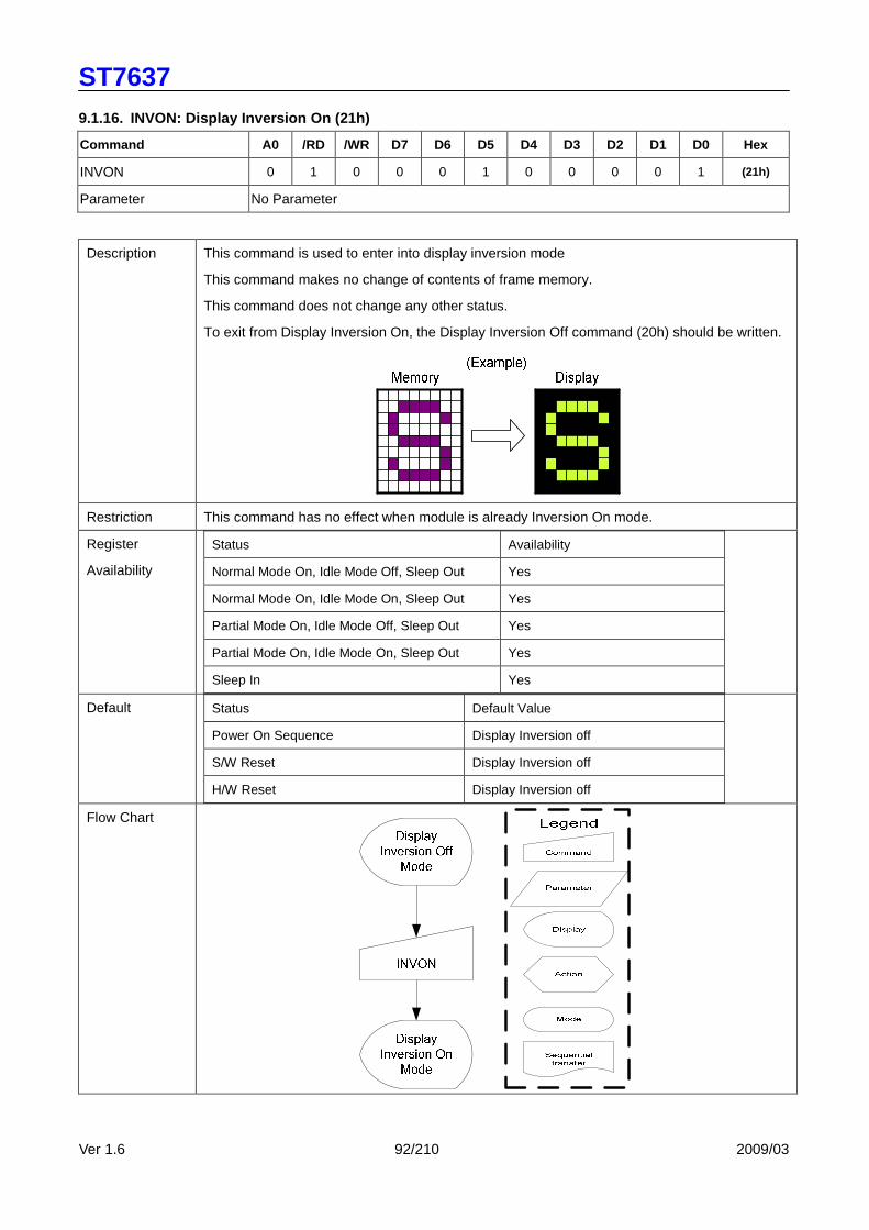
ST7637
Ver 1.6 92/210 2009/03
9.1.16. INVON: Display Inversion On (21h)
Command A0 /RD /WR D7 D6 D5 D4 D3 D2 D1 D0 Hex
INVON 0 1 0 0 0 1 0 0 0 0 1 (21h)
Parameter No Parameter
Description This command is used to enter into display inversion mode
This command makes no change of contents of frame memory.
This command does not change any other status.
To exit from Display Inversion On, the Display Inversion Off command (20h) should be written.
Restriction This command has no effect when module is already Inversion On mode.
Register
Availability
Status Availability
Normal Mode On, Idle Mode Off, Sleep Out Yes
Normal Mode On, Idle Mode On, Sleep Out Yes
Partial Mode On, Idle Mode Off, Sleep Out Yes
Partial Mode On, Idle Mode On, Sleep Out Yes
Sleep In Yes Default Status Default Value
Power On Sequence Display Inversion off
S/W Reset Display Inversion off
H/W Reset Display Inversion off Flow Chart

ST7637
Ver 1.6 93/210 2009/03
9.1.17. APOFF: All Pixels Off (22h) (Only for Test Purposes)
Command A0 /RD /WR D7 D6 D5 D4 D3 D2 D1 D0 Hex
APOFF 0 1 0 0 0 1 0 0 0 1 0 (22h)
Parameter No Parameter
Description This command is only used for test purpose e.g. pixel response time (on/off) measurements on
the passive matrix display. Therefore, it is possible that this command is not used for final
product software.
All driver outputs become “Low” data state and display becomes black.
This command makes no change of contents of display memory.
This command does not change any other status.
Exit commands are “All Pixels On”, “Normal Display Mode On” and “Partial Display On”.
The display is showing the contents of the frame memory after “Normal Display Mode On” and
“Partial Display On” commands.
Restriction This command has no effect when module is already All Pixel Off mode.
Register
Availability
Status Availability
Normal Mode On, Idle Mode Off, Sleep Out Yes
Normal Mode On, Idle Mode On, Sleep Out Yes
Partial Mode On, Idle Mode Off, Sleep Out Yes
Partial Mode On, Idle Mode On, Sleep Out Yes
Sleep In Yes Default Status Default Value
Power On Sequence All pixel off mode disable
S/W Reset All pixel off mode disable
H/W Reset All pixel off mode disable

ST7637
Ver 1.6 94/210 2009/03
Flow Chart
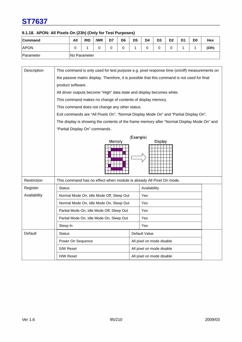
ST7637
Ver 1.6 95/210 2009/03
9.1.18. APON: All Pixels On (23h) (Only for Test Pu rposes)
Command A0 /RD /WR D7 D6 D5 D4 D3 D2 D1 D0 Hex
APON 0 1 0 0 0 1 0 0 0 1 1 (23h)
Parameter No Parameter
Description This command is only used for test purpose e.g. pixel response time (on/off) measurements on
the passive matrix display. Therefore, it is possible that this command is not used for final
product software.
All driver outputs become “High” data state and display becomes white.
This command makes no change of contents of display memory.
This command does not change any other status.
Exit commands are “All Pixels On”, “Normal Display Mode On” and “Partial Display On”.
The display is showing the contents of the frame memory after “Normal Display Mode On” and
“Partial Display On” commands.
Restriction This command has no effect when module is already All Pixel On mode.
Register
Availability
Status Availability
Normal Mode On, Idle Mode Off, Sleep Out Yes
Normal Mode On, Idle Mode On, Sleep Out Yes
Partial Mode On, Idle Mode Off, Sleep Out Yes
Partial Mode On, Idle Mode On, Sleep Out Yes
Sleep In Yes Default Status Default Value
Power On Sequence All pixel on mode disable
S/W Reset All pixel on mode disable
H/W Reset All pixel on mode disable
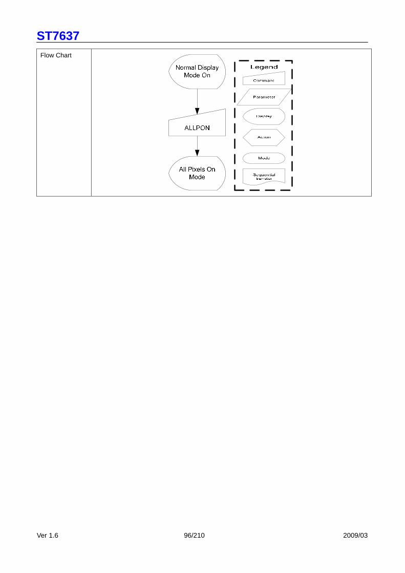
ST7637
Ver 1.6 96/210 2009/03
Flow Chart

ST7637
Ver 1.6 97/210 2009/03
9.1.19. WRCNTR: Write Contrast (25h)
Command A0 /RD /WR D7 D6 D5 D4 D3 D2 D1 D0 Hex
WRCNTR 0 1 0 0 0 1 0 0 1 0 1 (25h)
Parameter 1 1 0 0 EV6 EV5 EV4 EV3 EV2 EV1 EV0
Description This command is used to fine tuning the contrast of the display. Parameter range is 00~7Fh. The
contrast is not linear but the contrast adjustment is linear. Luminance is increasing from 00h to 7Fh.
00h is presenting dark end and 7Fh is presenting bright end.
Restriction -
Register
Availability
Status Availability
Normal Mode On, Idle Mode Off, Sleep Out Yes
Normal Mode On, Idle Mode On, Sleep Out Yes
Partial Mode On, Idle Mode Off, Sleep Out Yes
Partial Mode On, Idle Mode On, Sleep Out Yes
Sleep In Yes Default Status Default Value
Power On Sequence 3Fh
S/W Reset 3Fh
H/W Reset 3Fh Flow Chart

ST7637
Ver 1.6 98/210 2009/03
9.1.20. DISPOFF: Display Off (28h)
Command A0 /RD /WR D7 D6 D5 D4 D3 D2 D1 D0 Hex
DISPOFF 0 1 0 0 0 1 0 1 0 0 0 (28h)
Parameter No Parameter
Description This command is used to enter into DISPLAY OFF mode. In this mode, the output from Frame
Memory disables and blank page inserted.
This command makes no change of contents of frame memory.
This command does not change any other status.
There will be no abnormal visible effect on the display.
Exit from this command by Display On (29h)
Restriction This command has no effect when module is already in Display Off mode.
Register
Availability
Status Availability
Normal Mode On, Idle Mode Off, Sleep Out Yes
Normal Mode On, Idle Mode On, Sleep Out Yes
Partial Mode On, Idle Mode Off, Sleep Out Yes
Partial Mode On, Idle Mode On, Sleep Out Yes
Sleep In Yes Default Status Default Value
Power On Sequence Display off
S/W Reset Display off
H/W Reset Display off

ST7637
Ver 1.6 99/210 2009/03
Flow Chart
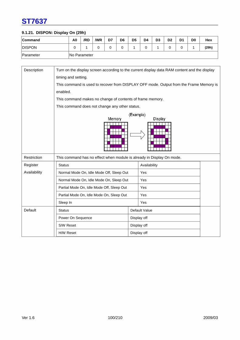
ST7637
Ver 1.6 100/210 2009/03
9.1.21. DISPON: Display On (29h)
Command A0 /RD /WR D7 D6 D5 D4 D3 D2 D1 D0 Hex
DISPON 0 1 0 0 0 1 0 1 0 0 1 (29h)
Parameter No Parameter
Description Turn on the display screen according to the current display data RAM content and the display
timing and setting.
This command is used to recover from DISPLAY OFF mode. Output from the Frame Memory is
enabled.
This command makes no change of contents of frame memory.
This command does not change any other status.
Restriction This command has no effect when module is already in Display On mode.
Register
Availability
Status Availability
Normal Mode On, Idle Mode Off, Sleep Out Yes
Normal Mode On, Idle Mode On, Sleep Out Yes
Partial Mode On, Idle Mode Off, Sleep Out Yes
Partial Mode On, Idle Mode On, Sleep Out Yes
Sleep In Yes Default Status Default Value
Power On Sequence Display off
S/W Reset Display off
H/W Reset Display off
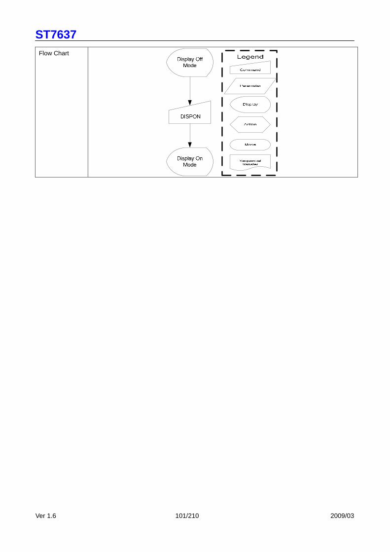
ST7637
Ver 1.6 101/210 2009/03
Flow Chart
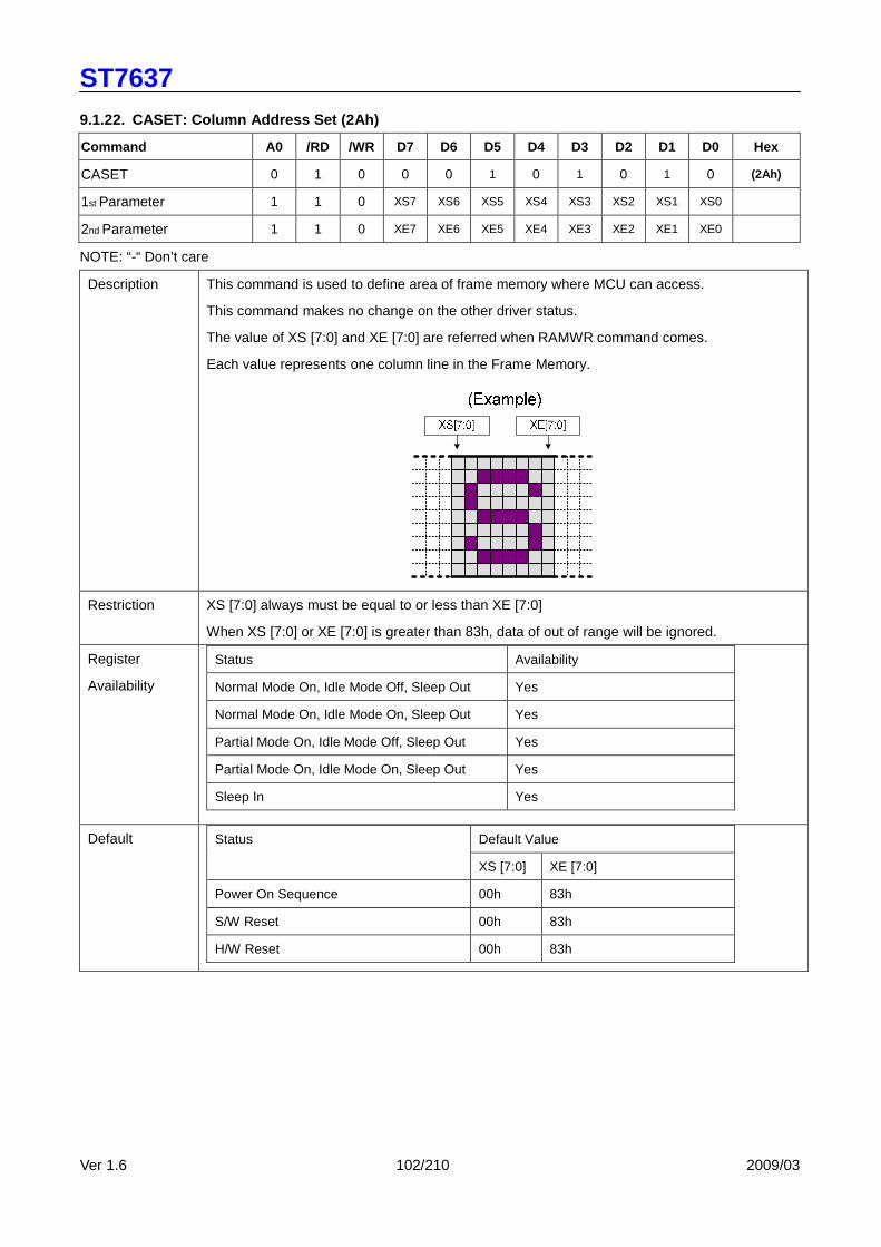
ST7637
Ver 1.6 102/210 2009/03
9.1.22. CASET: Column Address Set (2Ah)
Command A0 /RD /WR D7 D6 D5 D4 D3 D2 D1 D0 Hex
CASET 0 1 0 0 0 1 0 1 0 1 0 (2Ah)
1st Parameter 1 1 0 XS7 XS6 XS5 XS4 XS3 XS2 XS1 XS0
2nd Parameter 1 1 0 XE7 XE6 XE5 XE4 XE3 XE2 XE1 XE0
NOTE: “-“ Don’t care
Description This command is used to define area of frame memory where MCU can access.
This command makes no change on the other driver status.
The value of XS [7:0] and XE [7:0] are referred when RAMWR command comes.
Each value represents one column line in the Frame Memory.
Restriction XS [7:0] always must be equal to or less than XE [7:0]
When XS [7:0] or XE [7:0] is greater than 83h, data of out of range will be ignored.
Register
Availability
Status Availability
Normal Mode On, Idle Mode Off, Sleep Out Yes
Normal Mode On, Idle Mode On, Sleep Out Yes
Partial Mode On, Idle Mode Off, Sleep Out Yes
Partial Mode On, Idle Mode On, Sleep Out Yes
Sleep In Yes
Default Default Value Status
XS [7:0] XE [7:0]
Power On Sequence 00h 83h
S/W Reset 00h 83h
H/W Reset 00h 83h

ST7637
Ver 1.6 103/210 2009/03
Flow Chart CASET
1st parameter
XS[7:0]
2nd parameter
XE[7:0]
PASET
1st parameter
YS[7:0]
2nd parameter
YE[7:0]
RAMWR
Image Data D1[7:0],D2[7:0]…….Dn[7:0]
Any Command
If needed
ST7637
Ver 1.6 104/210 2009/03
9.1.23. RASET: Row Address Set (2Bh)
Command A0 /RD /WR D7 D6 D5 D4 D3 D2 D1 D0 Hex
RASET 0 1 0 0 0 1 0 1 0 1 1 (2Bh)
1st Parameter 1 1 0 YS7 YS6 YS5 YS4 YS3 YS2 YS1 YS0
2nd Parameter 1 1 0 YE7 YE6 YE5 YE4 YE3 YE2 YE1 YE0
NOTE: “-“ Don’t care
Description This command is used to define area of frame memory where MCU can access.
This command makes no change on the other driver status.
The value of YS [7:0] and YE [7:0] are referred when RAMWR command comes.
Each value represents one column line in the Frame Memory.
Restriction YS [7:0] always must be equal to or less than YE [7:0]
When YS [7:0] or YE [7:0] is greater than 83h, data of out of range will be ignored.
Register
Availability
Status Availability
Normal Mode On, Idle Mode Off, Sleep Out Yes
Normal Mode On, Idle Mode On, Sleep Out Yes
Partial Mode On, Idle Mode Off, Sleep Out Yes
Partial Mode On, Idle Mode On, Sleep Out Yes
Sleep In Yes
Default Default Value Status
XS [7:0] XE [7:0]
Power On Sequence 00h 83h
S/W Reset 00h 83h
H/W Reset 00h 83h

ST7637
Ver 1.6 105/210 2009/03
Flow Chart
CASET
1st parameter
XS[7:0]
2nd parameter
XE[7:0]
PASET
1st parameter
YS[7:0]
2nd parameter
YE[7:0]
RAMWR
Image Data D1[7:0],D2[7:0]…….Dn[7:0]
Any Command

ST7637
Ver 1.6 106/210 2009/03
9.1.24. RAMWR: Memory Write (2Ch)
Command A0 /RD /WR D7 D6 D5 D4 D3 D2 D1 D0 Hex
RAMWR 0 1 0 0 0 1 0 1 1 0 0 (2Ch)
Write D1[7:0] 1 1 0 D7 D6 D5 D4 D3 D2 D1 D0 -
: 1 1 0 : : : : : : : : -
Write Dn[7:0] 1 1 0 D7 D6 D5 D4 D3 D2 D1 D0 -
Description This command is used to transfer data MCU to frame memory.
This command makes no change to the other driver status.
When this command is accepted, the column register and the row register are reset to the Start
Column/Start Row positions.
The Start Column/Start Row positions are different in accordance with MADCTR setting. Then D
[7:0] is stored in frame memory and the column register and the row register incremented.
Frame Write can be canceled by sending any other command.
Restriction In all color modes, there is no restriction on length of parameters.
Register
Availability
Status Availability
Normal Mode On, Idle Mode Off, Sleep Out Yes
Normal Mode On, Idle Mode On, Sleep Out Yes
Partial Mode On, Idle Mode Off, Sleep Out Yes
Partial Mode On, Idle Mode On, Sleep Out Yes
Sleep In Yes
Default
Status Default Value
Power On Sequence Contents of memory is set randomly
S/W Reset Contents of memory is remained
H/W Reset Contents of memory is remained
Flow Chart
ST7637
Ver 1.6 107/210 2009/03
9.1.25. RGBSET: Colour Set for 256 or 4k-Color Disp lay (2Dh)
Command A0 /RD /WR D7 D6 D5 D4 D3 D2 D1 D0 Hex
RGBSET 0 1 0 0 0 1 0 1 1 0 1 (2Dh)
1st parameter 1 1 0 - - - R004 R003 R002 R001 R000 -
: 1 1 0 : : : Rnn4 Rnn3 Rnn2 Rnn1 Rnn0 -
16th parameter 1 1 0 - - - R154 R153 R152 R151 R150 -
17th parameter 1 1 0 - - G005 G004 G003 G002 G001 G000 -
: 1 1 0 : : Gnn5 Gnn4 Gnn3 Gnn2 Gnn1 Gnn0
32nd parameter 1 1 0 - - G155 G154 G153 G152 G151 G150
33rd parameter 1 1 0 - - - B004 B003 B002 B001 B000
: 1 1 0 : : : Bnn4 Bnn3 Bnn2 Bnn1 Bnn0
48th parameter 1 1 0 - - - B154 B153 B152 B151 B150
NOTE: “-“ Don’t care
Description This command is used to define the LUT for 8bit-to-16bit or 12bit-to-16bit color depth
conversations. (See also Section 7.9。)
48 Bytes must be written to the LUT regardless of the color mode. Only the values in Section
7.9。 are referred.
This command has no effect on other commands/parameters and Contents of frame memory.
Visible change takes effect next time the Frame Memory is written to.
Restriction Do not send any command before the last data is sent or LUT is not defined correctly.
Register
Availability
Status Availability
Normal Mode On, Idle Mode Off, Sleep Out Yes
Normal Mode On, Idle Mode On, Sleep Out Yes
Partial Mode On, Idle Mode Off, Sleep Out Yes
Partial Mode On, Idle Mode On, Sleep Out Yes
Sleep In Yes
Default
Status Default Value
Power On Sequence Refer to Section 7.9。
S/W Reset Contents of the look-up table protected
H/W Reset Refer to Section7.9。
ST7637
Ver 1.6 108/210 2009/03
Flow Chart
Command
Parameter
Display
Action
Mode
Legend
Sequential transter
REGSET
1st parameter R00[4:0]:
16th parameter R15[4:0]17th parameter G00[5:0]
:32nd parameter G15[5:0]33rd parameter B00[4:0]
:48th parameter B15[4:0]

ST7637
Ver 1.6 109/210 2009/03
9.1.26. RAMRO : Memory Read (2EH)
A0 RD WR D7 D6 D5 D4 D3 D2 D1 D0 HEX
Command 0 1 ↑ 0 0 1 0 1 1 1 0 (2Eh)
1st parameter 1 ↑ 1 x x x x x x x x x
2nd parameter 1 ↑ 1 D17 D16 D15 D14 D13 D12 D11 D10 00H ~ FFH
… 1 ↑ 1 Dx7 Dx6 Dx5 Dx4 Dx3 Dx2 Dx1 Dx0 00H ~ FFH
(N+1)th
parameter 1 ↑ 1 Dn7 Dn6 Dn5 Dn4 Dn3 Dn2 Dn1 Dn0 00H ~ FFH
Description This command is used to transfer data from frame memory to MCU. When this command is accepted,
the column register and the page register are reset to the Start Column/Start Page positions. The Start
Column/Start Page positions are different in accordance with MADCTR setting. Then D[7:0] is read
back from the frame memory and the column register and the page register incremented. Frame Read
can be stopped by sending any other command.
Restriction In all color modes, the Frame Read is always 16bit so there is no restriction on length of parameters.
Note: Memory Read is only possible via the Parallel Interface.
Register
Availability
Status Availability
Normal Mode On, Idle Mode Off, Sleep Out Yes
Normal Mode On, Idle Mode On, Sleep Out Yes
Partial Mode On, Idle Mode Off, Sleep Out Yes
Partial Mode On, Idle Mode On, Sleep Out Yes
Sleep In or Booster Off Yes
Default
Status Default Value
Power On Sequence Contents of memory is set randomly
S/W Reset Contents of memory is not cleared
H/W Reset Contents of memory is not cleared
ST7637
Ver 1.6 110/210 2009/03
Flow Chart
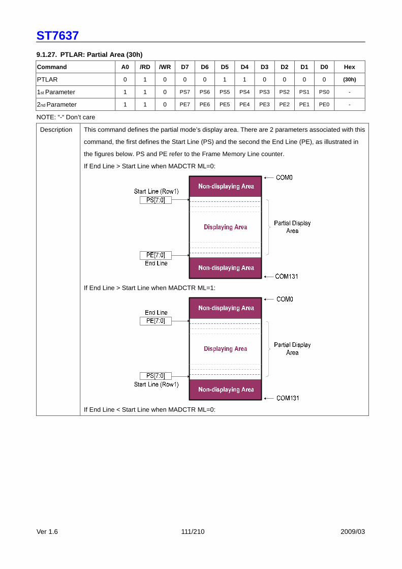
ST7637
Ver 1.6 111/210 2009/03
9.1.27. PTLAR: Partial Area (30h)
Command A0 /RD /WR D7 D6 D5 D4 D3 D2 D1 D0 Hex
PTLAR 0 1 0 0 0 1 1 0 0 0 0 (30h)
1st Parameter 1 1 0 PS7 PS6 PS5 PS4 PS3 PS2 PS1 PS0 -
2nd Parameter 1 1 0 PE7 PE6 PE5 PE4 PE3 PE2 PE1 PE0 -
NOTE: “-“ Don’t care
Description This command defines the partial mode’s display area. There are 2 parameters associated with this
command, the first defines the Start Line (PS) and the second the End Line (PE), as illustrated in
the figures below. PS and PE refer to the Frame Memory Line counter.
If End Line > Start Line when MADCTR ML=0:
If End Line > Start Line when MADCTR ML=1:
If End Line < Start Line when MADCTR ML=0:

ST7637
Ver 1.6 112/210 2009/03
* Row1: Frame memory row address 1.
If End Line = Start Line then the Partial Area will be one line deep.
Restriction PS[7:0] and PE[7:0] are based on line unit.
PS[6:0]=00h, 01h, 02h, 03h, … , 83h
PE[6:0]= 00h, 01h, 02h, 03h, … , 83h
Register
Availability
Status Availability
Normal Mode On, Idle Mode Off, Sleep Out Yes
Normal Mode On, Idle Mode On, Sleep Out Yes
Partial Mode On, Idle Mode Off, Sleep Out Yes
Partial Mode On, Idle Mode On, Sleep Out Yes
Sleep In Yes
Default
Default Value Status
PS[6:0] PE[6:0]
Power On Sequence 00h 83h
S/W Reset 00h 83h
H/W Reset 00h 83h

ST7637
Ver 1.6 113/210 2009/03
Flow Chart 1. TO Enter Partial Mode:
PLTAR
PS[7:0]
PE[7:0]
PTLON
Partial Mode
2. Leave Partial Mode
Partial Mode
DISPOFF
NORON
Partial Mode OFF
RAMRW
Image Data
D1[7:0],D2[7:0]
……..Dn[7:0]
DISPON
()ptional)
To prevent
Tearing Effect
Image displayed
Command
Parameter
Display
Action
Mode
Legend
Sequentialtranster
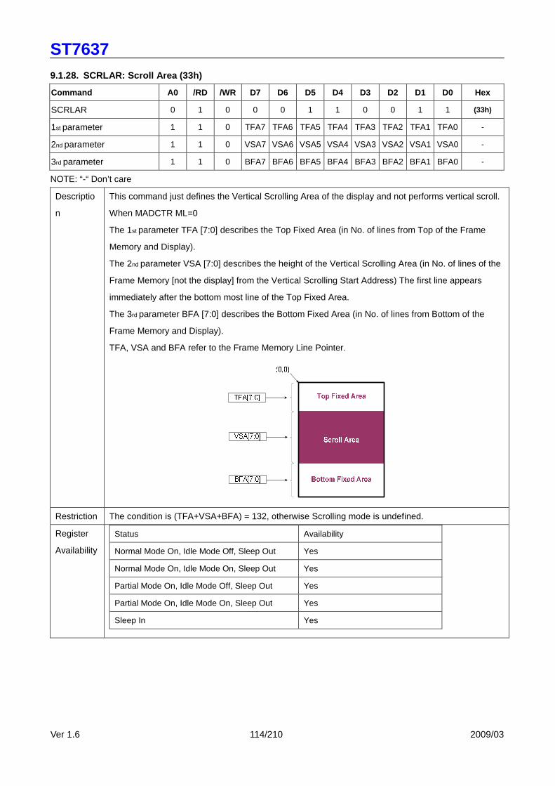
ST7637
Ver 1.6 114/210 2009/03
9.1.28. SCRLAR: Scroll Area (33h)
Command A0 /RD /WR D7 D6 D5 D4 D3 D2 D1 D0 Hex
SCRLAR 0 1 0 0 0 1 1 0 0 1 1 (33h)
1st parameter 1 1 0 TFA7 TFA6 TFA5 TFA4 TFA3 TFA2 TFA1 TFA0 -
2nd parameter 1 1 0 VSA7 VSA6 VSA5 VSA4 VSA3 VSA2 VSA1 VSA0 -
3rd parameter 1 1 0 BFA7 BFA6 BFA5 BFA4 BFA3 BFA2 BFA1 BFA0 -
NOTE: “-“ Don’t care
Descriptio
n
This command just defines the Vertical Scrolling Area of the display and not performs vertical scroll.
When MADCTR ML=0
The 1st parameter TFA [7:0] describes the Top Fixed Area (in No. of lines from Top of the Frame
Memory and Display).
The 2nd parameter VSA [7:0] describes the height of the Vertical Scrolling Area (in No. of lines of the
Frame Memory [not the display] from the Vertical Scrolling Start Address) The first line appears
immediately after the bottom most line of the Top Fixed Area.
The 3rd parameter BFA [7:0] describes the Bottom Fixed Area (in No. of lines from Bottom of the
Frame Memory and Display).
TFA, VSA and BFA refer to the Frame Memory Line Pointer.
Restriction The condition is (TFA+VSA+BFA) = 132, otherwise Scrolling mode is undefined.
Register
Availability
Status Availability
Normal Mode On, Idle Mode Off, Sleep Out Yes
Normal Mode On, Idle Mode On, Sleep Out Yes
Partial Mode On, Idle Mode Off, Sleep Out Yes
Partial Mode On, Idle Mode On, Sleep Out Yes
Sleep In Yes
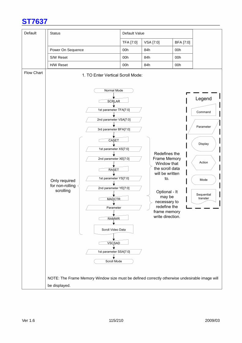
ST7637
Ver 1.6 115/210 2009/03
Default
Default Value Status
TFA [7:0] VSA [7:0] BFA [7:0]
Power On Sequence 00h 84h 00h
S/W Reset 00h 84h 00h
H/W Reset 00h 84h 00h
Flow Chart 1. TO Enter Vertical Scroll Mode:
Command
Parameter
Display
Action
Mode
Legend
Sequential
transter
Normal Mode
SCRLAR
1st parameter TFA[7:0]
2nd parameter VSA[7:0]
3rd parameter BFA[7:0]
CASET
1st parameter XS[7:0]
2nd parameter XE[7:0]
RASET
MADCTR
Parameter
RAMWR
Scroll Video Data
VSCSAD
1st parameter SSA[7:0]
Scroll Mode
1st parameter YS[7:0]
2nd parameter YE[7:0]
Only required
for non-rolling
scrolling
Redefines the
Frame Memory
Window that
the scroll data
will be written
to.
Optional - It
may be
necessary to
redefine the
frame memory
write direction.
NOTE: The Frame Memory Window size must be defined correctly otherwise undesirable image will
be displayed.
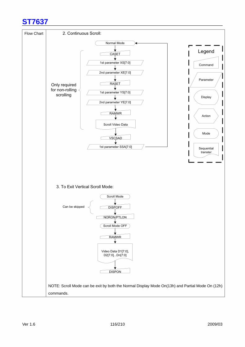
ST7637
Ver 1.6 116/210 2009/03
Flow Chart 2. Continuous Scroll:
Command
Parameter
Display
Action
Mode
Legend
Sequential
transter
Normal Mode
CASET
1st parameter XS[7:0]
2nd parameter XE[7:0]
RASET
RAMWR
Scroll Video Data
VSCSAD
1st parameter SSA[7:0]
1st parameter YS[7:0]
2nd parameter YE[7:0]
Only required
for non-rolling
scrolling
Scroll Mode
DISPOFF
NORON/PTLON
Scroll Mode OFF
RAMWR
Video Data D1[7:0],
D2[7:0]...Dn[7:0]
DISPON
3. To Exit Vertical Scroll Mode:
Can be skipped
NOTE: Scroll Mode can be exit by both the Normal Display Mode On(13h) and Partial Mode On (12h)
commands.
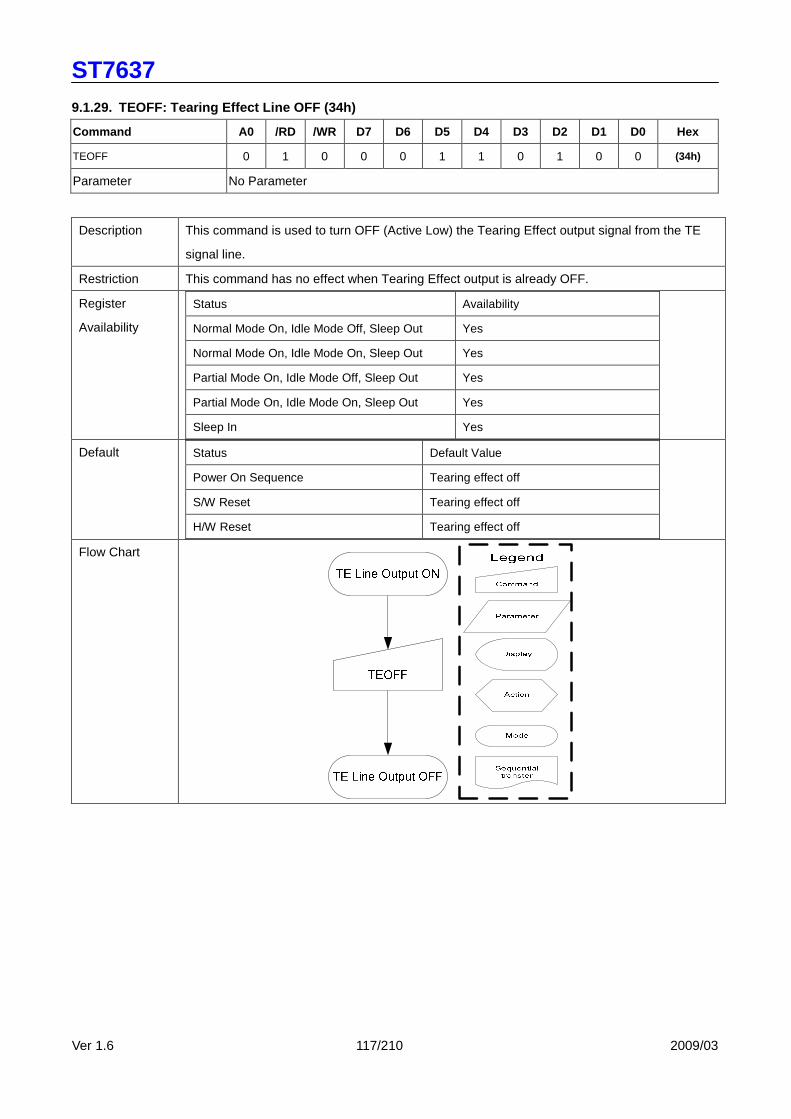
ST7637
Ver 1.6 117/210 2009/03
9.1.29. TEOFF: Tearing Effect Line OFF (34h)
Command A0 /RD /WR D7 D6 D5 D4 D3 D2 D1 D0 Hex
TEOFF 0 1 0 0 0 1 1 0 1 0 0 (34h)
Parameter No Parameter
Description This command is used to turn OFF (Active Low) the Tearing Effect output signal from the TE
signal line.
Restriction This command has no effect when Tearing Effect output is already OFF.
Register
Availability
Status Availability
Normal Mode On, Idle Mode Off, Sleep Out Yes
Normal Mode On, Idle Mode On, Sleep Out Yes
Partial Mode On, Idle Mode Off, Sleep Out Yes
Partial Mode On, Idle Mode On, Sleep Out Yes
Sleep In Yes Default Status Default Value
Power On Sequence Tearing effect off
S/W Reset Tearing effect off
H/W Reset Tearing effect off Flow Chart
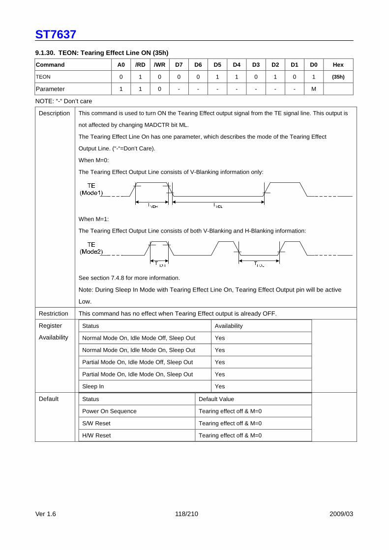
ST7637
Ver 1.6 118/210 2009/03
9.1.30. TEON: Tearing Effect Line ON (35h)
Command A0 /RD /WR D7 D6 D5 D4 D3 D2 D1 D0 Hex
TEON 0 1 0 0 0 1 1 0 1 0 1 (35h)
Parameter 1 1 0 - - - - - - - M
NOTE: “-“ Don’t care
Description This command is used to turn ON the Tearing Effect output signal from the TE signal line. This output is
not affected by changing MADCTR bit ML.
The Tearing Effect Line On has one parameter, which describes the mode of the Tearing Effect
Output Line. (“-“=Don’t Care).
When M=0:
The Tearing Effect Output Line consists of V-Blanking information only:
When M=1:
The Tearing Effect Output Line consists of both V-Blanking and H-Blanking information:
See section 7.4.8 for more information.
Note: During Sleep In Mode with Tearing Effect Line On, Tearing Effect Output pin will be active
Low.
Restriction This command has no effect when Tearing Effect output is already OFF.
Register
Availability
Status Availability
Normal Mode On, Idle Mode Off, Sleep Out Yes
Normal Mode On, Idle Mode On, Sleep Out Yes
Partial Mode On, Idle Mode Off, Sleep Out Yes
Partial Mode On, Idle Mode On, Sleep Out Yes
Sleep In Yes Default Status Default Value
Power On Sequence Tearing effect off & M=0
S/W Reset Tearing effect off & M=0
H/W Reset Tearing effect off & M=0

ST7637
Ver 1.6 119/210 2009/03
Flow Chart
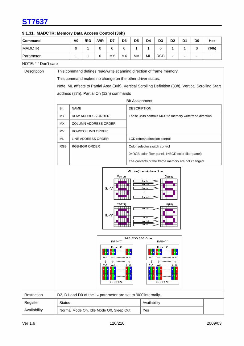
ST7637
Ver 1.6 120/210 2009/03
9.1.31. MADCTR: Memory Data Access Control (36h)
Command A0 /RD /WR D7 D6 D5 D4 D3 D2 D1 D0 Hex
MADCTR 0 1 0 0 0 1 1 0 1 1 0 (36h)
Parameter 1 1 0 MY MX MV ML RGB - - - -
NOTE: “-“ Don’t care
Description This command defines read/write scanning direction of frame memory.
This command makes no change on the other driver status.
Note: ML affects to Partial Area (30h), Vertical Scrolling Definition (33h), Vertical Scrolling Start
address (37h), Partial On (12h) commands
Bit Assignment
Bit NAME DESCRIPTION
MY ROW ADDRESS ORDER
MX COLUMN ADDRESS ORDER
MV ROW/COLUMN ORDER
These 3bits controls MCU to memory write/read direction.
ML LINE ADDRESS ORDER LCD refresh direction control
RGB RGB-BGR ORDER Color selector switch control
0=RGB color filter panel, 1=BGR color filter panel)
The contents of the frame memory are not changed.
Restriction D2, D1 and D0 of the 1st parameter are set to ‘000’internally.
Register
Availability
Status Availability
Normal Mode On, Idle Mode Off, Sleep Out Yes

ST7637
Ver 1.6 121/210 2009/03
Normal Mode On, Idle Mode On, Sleep Out Yes
Partial Mode On, Idle Mode Off, Sleep Out Yes
Partial Mode On, Idle Mode On, Sleep Out Yes
Sleep In Yes Default Status Default Value
Power On Sequence MY=0,MX=0,MV=0,ML=0,RGB=0
S/W Reset Not changed
H/W Reset MY=0,MX=0,MV=0,ML=0,RGB=0 Flow Chart

ST7637
Ver 1.6 122/210 2009/03
9.1.32. VSCSAD: Vertical Scroll Start Address of RA M (37h)
Command A0 /RD /WR D7 D6 D5 D4 D3 D2 D1 D0 Hex
VSCSAD 0 1 0 0 0 1 1 0 1 1 1 (37h)
Parameter 1 1 0 SSA7 SSA6 SSA5 SSA4 SSA3 SSA2 SSA1 SSA0
Description
This command is used together with Vertical Scrolling Definition (33h). These two commands
describe the scrolling area and the scrolling mode.
The Vertical Scrolling Start Address command has one parameter which describes which line in
the Frame Memory will be written as the first line after the last line of the Top Fixed Area on the
display as illustrated below:
This command Start the scrolling.
Exit from V-scrolling mode by commands Partial mode On (12h) or Normal mode On (13h).
When MADCTR ML=0
Example:
When Top Fixed Area=Bottom Fixed Area=00, Vertical Scrolling Area=132 and Vertical Scrolling
Pointer SSA=’3’.
Memory
SSA [7:0]
Scroll start address
(0,0)
(0,131)
0123
131130
DisplayCOM0
COM1
COM2
COM129
COM131
COM130
Scan address
When MADCTR ML=1
Example:
When Top Fixed Area=Bottom Fixed Area=00, Vertical Scrolling Area=132 and Vertical Scrolling
Pointer SSA=’3’.
NOTE: When new Pointer position and Picture Data are sent, the result on the display will
happen at the next Panel Scan to avoid tearing effect.
SSA refers to the Frame Memory line Pointer.
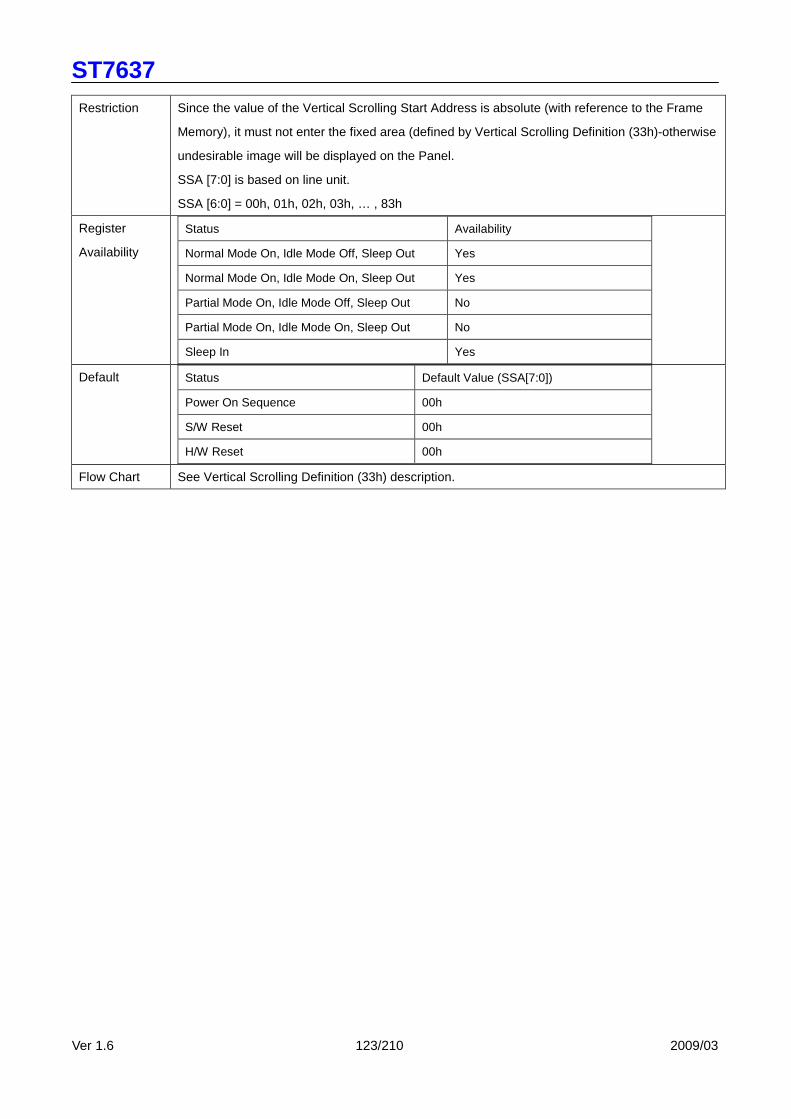
ST7637
Ver 1.6 123/210 2009/03
Restriction Since the value of the Vertical Scrolling Start Address is absolute (with reference to the Frame
Memory), it must not enter the fixed area (defined by Vertical Scrolling Definition (33h)-otherwise
undesirable image will be displayed on the Panel.
SSA [7:0] is based on line unit.
SSA [6:0] = 00h, 01h, 02h, 03h, … , 83h
Register
Availability
Status Availability
Normal Mode On, Idle Mode Off, Sleep Out Yes
Normal Mode On, Idle Mode On, Sleep Out Yes
Partial Mode On, Idle Mode Off, Sleep Out No
Partial Mode On, Idle Mode On, Sleep Out No
Sleep In Yes Default Status Default Value (SSA[7:0])
Power On Sequence 00h
S/W Reset 00h
H/W Reset 00h Flow Chart See Vertical Scrolling Definition (33h) description.
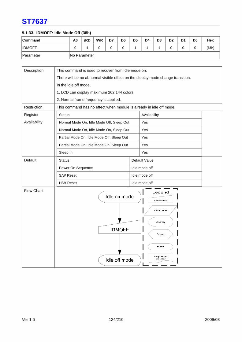
ST7637
Ver 1.6 124/210 2009/03
9.1.33. IDMOFF: Idle Mode Off (38h)
Command A0 /RD /WR D7 D6 D5 D4 D3 D2 D1 D0 Hex
IDMOFF 0 1 0 0 0 1 1 1 0 0 0 (38h)
Parameter No Parameter
Description This command is used to recover from Idle mode on.
There will be no abnormal visible effect on the display mode change transition.
In the idle off mode,
1. LCD can display maximum 262,144 colors.
2. Normal frame frequency is applied.
Restriction This command has no effect when module is already in idle off mode.
Register
Availability
Status Availability
Normal Mode On, Idle Mode Off, Sleep Out Yes
Normal Mode On, Idle Mode On, Sleep Out Yes
Partial Mode On, Idle Mode Off, Sleep Out Yes
Partial Mode On, Idle Mode On, Sleep Out Yes
Sleep In Yes Default Status Default Value
Power On Sequence Idle mode off
S/W Reset Idle mode off
H/W Reset Idle mode off Flow Chart
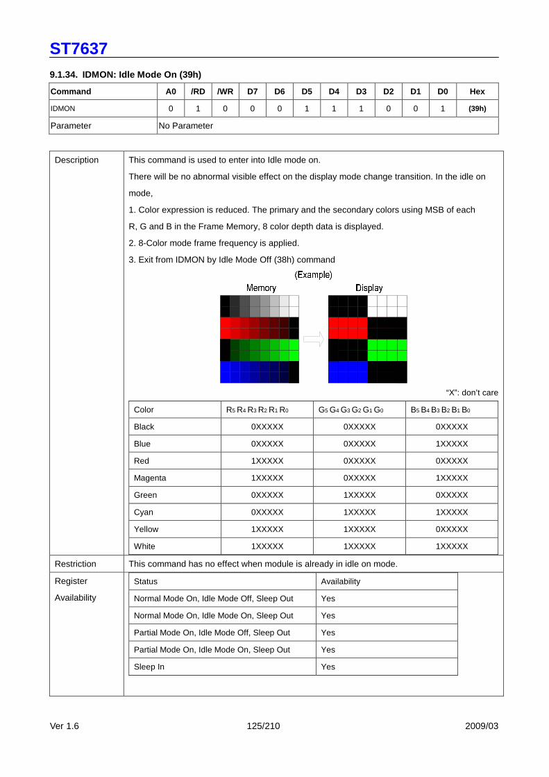
ST7637
Ver 1.6 125/210 2009/03
9.1.34. IDMON: Idle Mode On (39h)
Command A0 /RD /WR D7 D6 D5 D4 D3 D2 D1 D0 Hex
IDMON 0 1 0 0 0 1 1 1 0 0 1 (39h)
Parameter No Parameter
Description This command is used to enter into Idle mode on.
There will be no abnormal visible effect on the display mode change transition. In the idle on
mode,
1. Color expression is reduced. The primary and the secondary colors using MSB of each
R, G and B in the Frame Memory, 8 color depth data is displayed.
2. 8-Color mode frame frequency is applied.
3. Exit from IDMON by Idle Mode Off (38h) command
“X”: don’t care
Color R5 R4 R3 R2 R1 R0 G5 G4 G3 G2 G1 G0 B5 B4 B3 B2 B1 B0
Black 0XXXXX 0XXXXX 0XXXXX
Blue 0XXXXX 0XXXXX 1XXXXX
Red 1XXXXX 0XXXXX 0XXXXX
Magenta 1XXXXX 0XXXXX 1XXXXX
Green 0XXXXX 1XXXXX 0XXXXX
Cyan 0XXXXX 1XXXXX 1XXXXX
Yellow 1XXXXX 1XXXXX 0XXXXX
White 1XXXXX 1XXXXX 1XXXXX
Restriction This command has no effect when module is already in idle on mode.
Register
Availability
Status Availability
Normal Mode On, Idle Mode Off, Sleep Out Yes
Normal Mode On, Idle Mode On, Sleep Out Yes
Partial Mode On, Idle Mode Off, Sleep Out Yes
Partial Mode On, Idle Mode On, Sleep Out Yes
Sleep In Yes

ST7637
Ver 1.6 126/210 2009/03
Default Status Default Value
Power On Sequence Idle mode off
S/W Reset Idle mode off
H/W Reset Idle mode off Flow Chart

ST7637
Ver 1.6 127/210 2009/03
9.1.35. COLMOD: Interface Pixel Format (3Ah)
Command A0 /RD /WR D7 D6 D5 D4 D3 D2 D1 D0 Hex
COLMOD 0 1 0 0 0 1 1 1 0 1 0 (3Ah)
Parameter 1 1 0 - - - - - P2 P1 P0 -
Description This command is used to define the format of RGB picture data, which is to be transferred via
the MCU Interface. The formats are shown in the table:
Note: In 8 bit/pixel, 12bit/pixe,l or 16 bit/pixel mode, the LUT is applied to transfer data into the
Frame Memory.
Interface Format P2 P1 P0
Not Defined 0 0 0
Not Defined 0 0 1
8Bit/Pixel 0 1 0
12Bit/Pixel (Type A) 0 1 1
12Bit/Pixel (Type B) 1 0 0
16Bit/Pixel 1 0 1
18Bit/Pixel 1 1 0
24Bit/Pixel 1 1 1
Restriction There is no visible effect until the Frame Memory is written to.
Register
Availability
Status Availability
Normal Mode On, Idle Mode Off, Sleep Out Yes
Normal Mode On, Idle Mode On, Sleep Out Yes
Partial Mode On, Idle Mode Off, Sleep Out Yes
Partial Mode On, Idle Mode On, Sleep Out Yes
Sleep In Yes Default Status Default Value
Power On Sequence 05h (16Bit/Pixel)
S/W Reset No Change
H/W Reset 05h (16Bit/Pixel)

ST7637
Ver 1.6 128/210 2009/03
Flow Chart 16 Bit/Pixel Mode
COLMOD
011
12 Bit/Pixel Mode
Example:
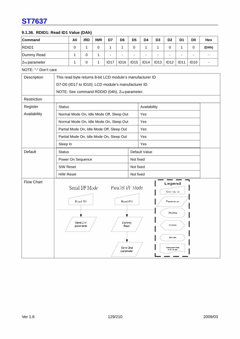
ST7637
Ver 1.6 129/210 2009/03
9.1.36. RDID1: Read ID1 Value (DAh)
Command A0 /RD /WR D7 D6 D5 D4 D3 D2 D1 D0 Hex
RDID1 0 1 0 1 1 0 1 1 0 1 0 (DAh)
Dummy Read 1 0 1 - - - - - - - - -
2nd parameter 1 0 1 ID17 ID16 ID15 ID14 ID13 ID12 ID11 ID10 -
NOTE: “-“ Don’t care
Description This read byte returns 8-bit LCD module’s manufacturer ID
D7-D0 (ID17 to ID10): LCD module’s manufacturer ID.
NOTE: See command RDDID (04h), 2nd parameter.
Restriction
Register
Availability
Status Availability
Normal Mode On, Idle Mode Off, Sleep Out Yes
Normal Mode On, Idle Mode On, Sleep Out Yes
Partial Mode On, Idle Mode Off, Sleep Out Yes
Partial Mode On, Idle Mode On, Sleep Out Yes
Sleep In Yes Default Status Default Value
Power On Sequence Not fixed
S/W Reset Not fixed
H/W Reset Not fixed Flow Chart

ST7637
Ver 1.6 130/210 2009/03
9.1.37. RDID2: Read ID2 Value (DBh)
Command A0 /RD /WR D7 D6 D5 D4 D3 D2 D1 D0 Hex
RDID2 0 1 0 1 1 0 1 1 0 1 1 (DBh)
Dummy Read 1 0 1 - - - - - - - - -
2nd parameter 1 0 1 ID27 ID26 ID25 ID24 ID23 ID22 ID21 ID20 -
NOTE: “-“ Don’t care
Description This read byte returns 8-bit LCD module/driver version ID
D7-D0 (ID27 to ID20): LCD module/driver version ID
Parameter Range: ID=80h to FFh
NOTE: See command RDDID (04h), 3rd parameter.
Restriction
Register
Availability
Status Availability
Normal Mode On, Idle Mode Off, Sleep Out Yes
Normal Mode On, Idle Mode On, Sleep Out Yes
Partial Mode On, Idle Mode Off, Sleep Out Yes
Partial Mode On, Idle Mode On, Sleep Out Yes
Sleep In Yes Default Status Default Value
Power On Sequence Not fixed
S/W Reset Not fixed
H/W Reset Not fixed Flow Chart

ST7637
Ver 1.6 131/210 2009/03
9.1.38. RDID3: Read ID3 Value (DCh)
Command A0 /RD /WR D7 D6 D5 D4 D3 D2 D1 D0 Hex
RDID3 0 1 0 1 1 0 1 1 1 0 0 (DCh)
Dummy Read 1 0 1 - - - - - - - - -
2nd parameter 1 0 1 ID37 ID36 ID35 ID34 ID33 ID32 ID31 ID30 -
NOTE: “-“ Don’t care
Description This read byte returns 8-bit LCD module/driver ID.
D7-D0 (ID37 to ID30): LCD module/driver ID.
NOTE: See command RDDID (04h), 4th parameter.
Restriction
Register
Availability
Status Availability
Normal Mode On, Idle Mode Off, Sleep Out Yes
Normal Mode On, Idle Mode On, Sleep Out Yes
Partial Mode On, Idle Mode Off, Sleep Out Yes
Partial Mode On, Idle Mode On, Sleep Out Yes
Sleep In Yes Default Status Default Value
Power On Sequence Not fixed
S/W Reset Not fixed
H/W Reset Not fixed Flow Chart
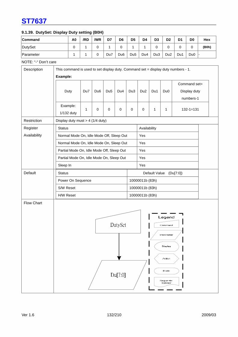
ST7637
Ver 1.6 132/210 2009/03
9.1.39. DutySet: Display Duty setting (B0H)
Command A0 /RD /WR D7 D6 D5 D4 D3 D2 D1 D0 Hex
DutySet 0 1 0 1 0 1 1 0 0 0 0 (B0h)
Parameter 1 1 0 Du7 Du6 Du5 Du4 Du3 Du2 Du1 Du0 -
NOTE: “-“ Don’t care
Description This command is used to set display duty. Command set = display duty numbers - 1.
Example:
Duty Du7 Du6 Du5 Du4 Du3 Du2 Du1 Du0
Command set=
Display duty
numbers-1
Example:
1/132 duty 1 0 0 0 0 0 1 1 132-1=131
Restriction Display duty must > 4 (1/4 duty)
Register
Availability
Status Availability
Normal Mode On, Idle Mode Off, Sleep Out Yes
Normal Mode On, Idle Mode On, Sleep Out Yes
Partial Mode On, Idle Mode Off, Sleep Out Yes
Partial Mode On, Idle Mode On, Sleep Out Yes
Sleep In Yes Default Status Default Value (Du[7:0])
Power On Sequence 10000011b (83h)
S/W Reset 10000011b (83h)
H/W Reset 10000011b (83h) Flow Chart

ST7637
Ver 1.6 133/210 2009/03
9.1.40. FirstCom: First Com. Page address (B1H)
Command A0 /RD /WR D7 D6 D5 D4 D3 D2 D1 D0 Hex
FirstCom 0 1 0 1 0 1 1 0 0 0 1 (B1h)
Parameter 1 1 0 F7 F6 F5 F4 F3 F2 F1 F0 -
NOTE: “-“ Don’t care
Description This command defines the first output COM number that mapping to the RAM page
address 0. For detail setting value, please see the table as below.
F7 F6 F5 F4 F3 F2 F1 F0 Line address 0 0 0 0 0 0 0 0 0 0 0 0 1 1 0 0 0 0 1 0 2 0 0 0 0 1 1 3 0 : : : : : : 1 0 0 0 0 0 1 1 131
Example:
If FirstCom=8, common 8 would output the data of RAM page address 0.
Restriction
Register
Availability
Status Availability
Normal Mode On, Idle Mode Off, Sleep Out Yes
Normal Mode On, Idle Mode On, Sleep Out Yes
Partial Mode On, Idle Mode Off, Sleep Out Yes
Partial Mode On, Idle Mode On, Sleep Out Yes
Sleep In Yes Default Status Default Value (F[7:0])
Power On Sequence 00h
S/W Reset 00h
H/W Reset 00h Flow Chart

ST7637
Ver 1.6 134/210 2009/03
9.1.41. OscDiv: FOSC Divider (B3H)
Command A0 /RD /WR D7 D6 D5 D4 D3 D2 D1 D0 Hex
OscDiv 0 1 0 1 0 1 1 0 0 1 1 (B3h)
Parameter 1 1 0 - - - - - - CLD1 CLD0 -
NOTE: “-“ Don’t care
Description This command is used to specify the Fosc dividing ratio.
CLD1, CLD0: Fosc dividing ratio. They are used to change number of dividing stages of internal
clock.
CLD1 CLD0 Fosc dividing ratio
0 0
0 1
1 0
1 1
Not divide
2 divisions
4 divisions
8 divisions
Restriction
Register
Availability
Status Availability
Normal Mode On, Idle Mode Off, Sleep Out Yes
Normal Mode On, Idle Mode On, Sleep Out Yes
Partial Mode On, Idle Mode Off, Sleep Out Yes
Partial Mode On, Idle Mode On, Sleep Out Yes
Sleep In Yes Default Status Default Value (CLD[0:1])
Power On Sequence 00b
S/W Reset 00b
H/W Reset 00b Flow Chart

ST7637
Ver 1.6 135/210 2009/03
9.1.42. NLInvSet: N-Line control (B5H)
Command A0 /RD /WR D7 D6 D5 D4 D3 D2 D1 D0 Hex
NLInvSet 0 1 0 1 0 1 1 0 1 0 1 (B5h)
Parameter 1 1 0 M N6 N5 N4 N3 N2 N1 N0 -
NOTE: “-“ Don’t care
Description This command is used to set the inverted line number with range of 2 to (duty-1) to improve display
quality. When M=0, inversion occurs in every frame; when M=1, inversion is independent from
frames. If N[6:0]=0, N-line inversion function is disable.
Line inversion numbers=N[6:0] +1.
Example:
If N[6:0]=7, inversion occurs per 8 line.
Restriction
Register
Availability
Status Availability
Normal Mode On, Idle Mode Off, Sleep Out Yes
Normal Mode On, Idle Mode On, Sleep Out Yes
Partial Mode On, Idle Mode Off, Sleep Out Yes
Partial Mode On, Idle Mode On, Sleep Out Yes
Sleep In Yes
Default
Default Value Status
M N[6:0]
Power On Sequence 0b 0000000b
S/W Reset 0b 0000000b
H/W Reset 0b 0000000b
Flow Chart
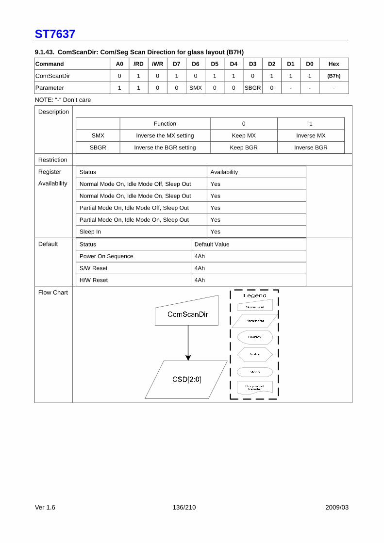
ST7637
Ver 1.6 136/210 2009/03
9.1.43. ComScanDir: Com/Seg Scan Direction for glas s layout (B7H)
Command A0 /RD /WR D7 D6 D5 D4 D3 D2 D1 D0 Hex
ComScanDir 0 1 0 1 0 1 1 0 1 1 1 (B7h)
Parameter 1 1 0 0 SMX 0 0 SBGR 0 - - -
NOTE: “-“ Don’t care
Description
Function 0 1
SMX Inverse the MX setting Keep MX Inverse MX
SBGR Inverse the BGR setting Keep BGR Inverse BGR
Restriction
Register
Availability
Status Availability
Normal Mode On, Idle Mode Off, Sleep Out Yes
Normal Mode On, Idle Mode On, Sleep Out Yes
Partial Mode On, Idle Mode Off, Sleep Out Yes
Partial Mode On, Idle Mode On, Sleep Out Yes
Sleep In Yes Default Status Default Value
Power On Sequence 4Ah
S/W Reset 4Ah
H/W Reset 4Ah Flow Chart
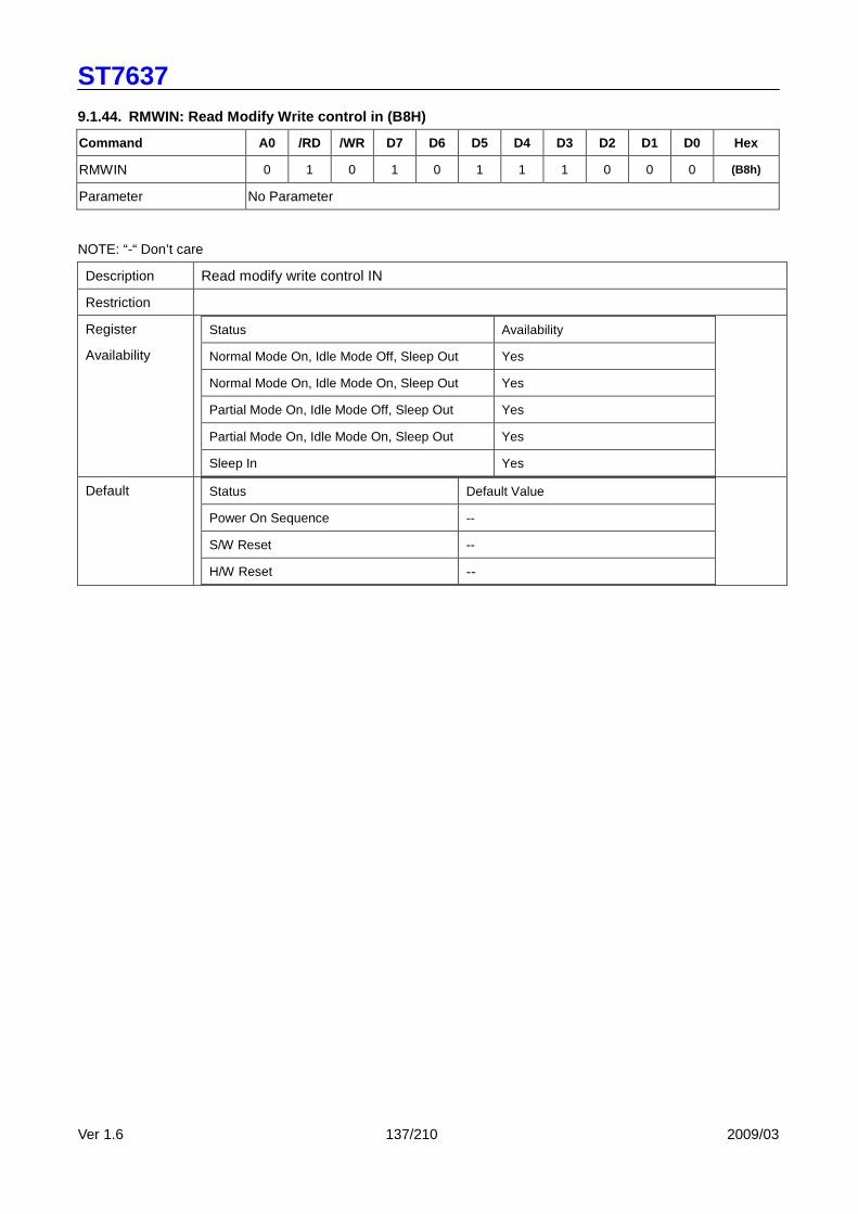
ST7637
Ver 1.6 137/210 2009/03
9.1.44. RMWIN: Read Modify Write control in (B8H)
Command A0 /RD /WR D7 D6 D5 D4 D3 D2 D1 D0 Hex
RMWIN 0 1 0 1 0 1 1 1 0 0 0 (B8h)
Parameter No Parameter
NOTE: “-“ Don’t care
Description Read modify write control IN
Restriction
Register
Availability
Status Availability
Normal Mode On, Idle Mode Off, Sleep Out Yes
Normal Mode On, Idle Mode On, Sleep Out Yes
Partial Mode On, Idle Mode Off, Sleep Out Yes
Partial Mode On, Idle Mode On, Sleep Out Yes
Sleep In Yes Default Status Default Value
Power On Sequence --
S/W Reset --
H/W Reset --

ST7637
Ver 1.6 138/210 2009/03
9.1.45. RMWOUT: Read Modify Write control out(B9H)
Command A0 /RD /WR D7 D6 D5 D4 D3 D2 D1 D0 Hex
RMWOUT 0 1 0 1 0 1 1 1 0 0 1 (B9h)
Parameter No Parameter
NOTE: “-“ Don’t care
Description Read modify write control OUT
Restriction
Register
Availability
Status Availability
Normal Mode On, Idle Mode Off, Sleep Out Yes
Normal Mode On, Idle Mode On, Sleep Out Yes
Partial Mode On, Idle Mode Off, Sleep Out Yes
Partial Mode On, Idle Mode On, Sleep Out Yes
Sleep In Yes Default Status Default Value
Power On Sequence --
S/W Reset --
H/W Reset --

ST7637
Ver 1.6 139/210 2009/03
9.1.46. VopSet: Vop set (C0H)
Command A0 /RD /WR D7 D6 D5 D4 D3 D2 D1 D0 Hex
VopSet 0 1 0 1 1 0 0 0 0 0 0 (C0h)
1st parameter 1 1 0 Vop7 Vop6 Vop5 Vop4 Vop3 Vop2 Vop1 Vop0 -
2nd parameter 1 1 0 - - - - - - - Vop8
NOTE: “-“ Don’t care
Description The command is used to program the optimum LCD supply voltage V0. Please see Section 7.10
for reference.
Restriction
Register
Availability
Status Availability
Normal Mode On, Idle Mode Off, Sleep Out Yes
Normal Mode On, Idle Mode On, Sleep Out Yes
Partial Mode On, Idle Mode Off, Sleep Out Yes
Partial Mode On, Idle Mode On, Sleep Out Yes
Sleep In Yes Default Status Default Value (Vop=12V)
Vop8 Vop[7:0]
Power On Sequence 0 11010010b (D2h)
S/W Reset 0 11010010b (D2h)
H/W Reset 0 11010010b (D2h) Flow Chart
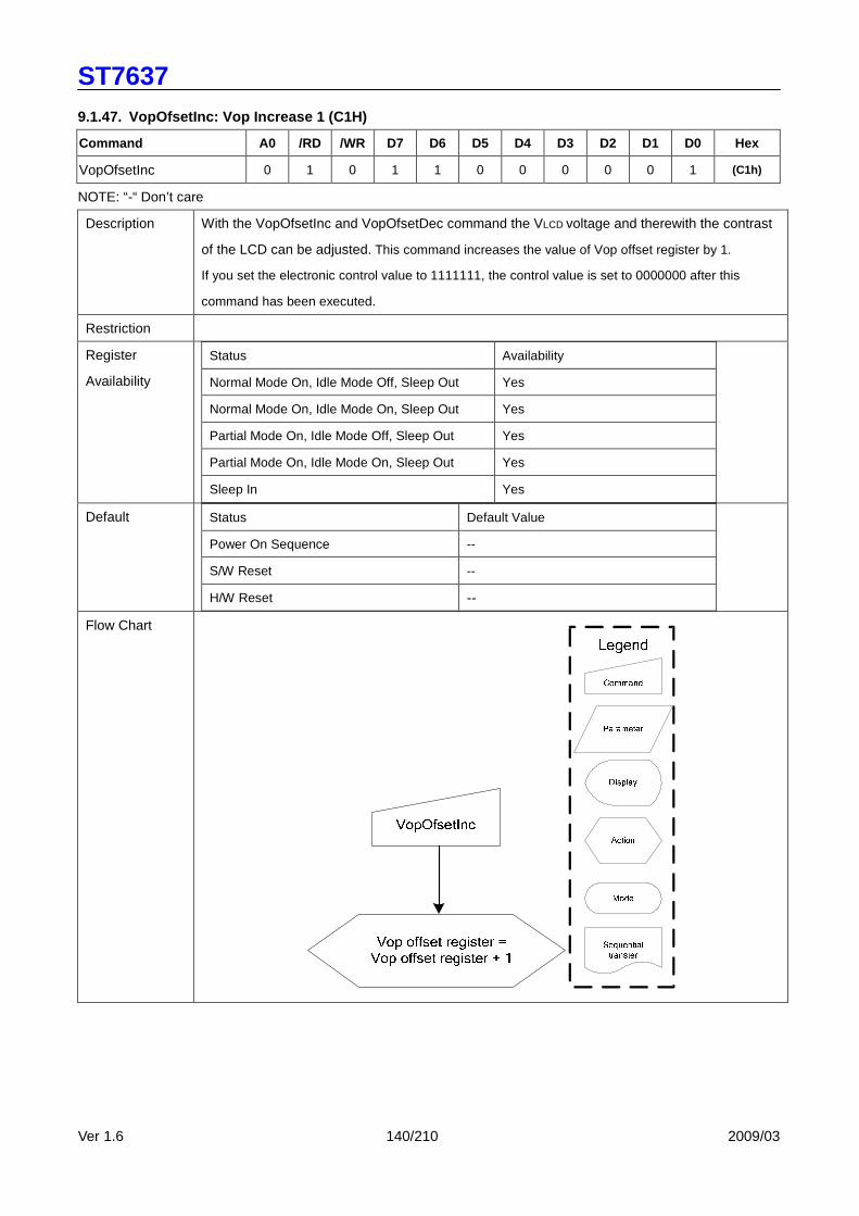
ST7637
Ver 1.6 140/210 2009/03
9.1.47. VopOfsetInc: Vop Increase 1 (C1H)
Command A0 /RD /WR D7 D6 D5 D4 D3 D2 D1 D0 Hex
VopOfsetInc 0 1 0 1 1 0 0 0 0 0 1 (C1h)
NOTE: “-“ Don’t care
Description With the VopOfsetInc and VopOfsetDec command the VLCD voltage and therewith the contrast
of the LCD can be adjusted. This command increases the value of Vop offset register by 1.
If you set the electronic control value to 1111111, the control value is set to 0000000 after this
command has been executed.
Restriction
Register
Availability
Status Availability
Normal Mode On, Idle Mode Off, Sleep Out Yes
Normal Mode On, Idle Mode On, Sleep Out Yes
Partial Mode On, Idle Mode Off, Sleep Out Yes
Partial Mode On, Idle Mode On, Sleep Out Yes
Sleep In Yes Default Status Default Value
Power On Sequence --
S/W Reset --
H/W Reset -- Flow Chart
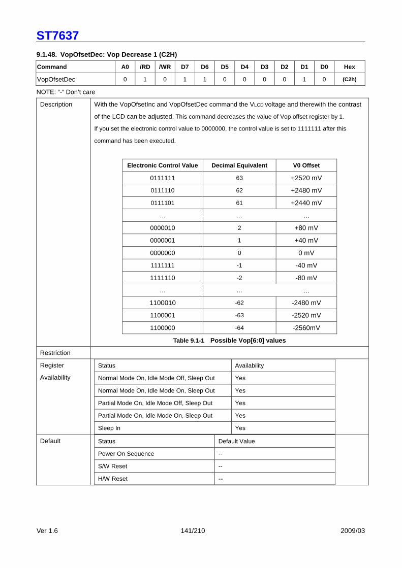
ST7637
Ver 1.6 141/210 2009/03
9.1.48. VopOfsetDec: Vop Decrease 1 (C2H)
Command A0 /RD /WR D7 D6 D5 D4 D3 D2 D1 D0 Hex
VopOfsetDec 0 1 0 1 1 0 0 0 0 1 0 (C2h)
NOTE: “-“ Don’t care
Description With the VopOfsetInc and VopOfsetDec command the VLCD voltage and therewith the contrast
of the LCD can be adjusted. This command decreases the value of Vop offset register by 1.
If you set the electronic control value to 0000000, the control value is set to 1111111 after this
command has been executed.
Electronic Control Value Decimal Equivalent V0 Offset
0111111 63 +2520 mV
0111110 62 +2480 mV
0111101 61 +2440 mV
… … …
0000010 2 +80 mV
0000001 1 +40 mV
0000000 0 0 mV
1111111 -1 -40 mV
1111110 -2 -80 mV
… … …
1100010 -62 -2480 mV
1100001 -63 -2520 mV
1100000 -64 -2560mV
Table 9.1-1 Possible Vop[6:0] values
Restriction
Register
Availability
Status Availability
Normal Mode On, Idle Mode Off, Sleep Out Yes
Normal Mode On, Idle Mode On, Sleep Out Yes
Partial Mode On, Idle Mode Off, Sleep Out Yes
Partial Mode On, Idle Mode On, Sleep Out Yes
Sleep In Yes Default Status Default Value
Power On Sequence --
S/W Reset --
H/W Reset --

ST7637
Ver 1.6 142/210 2009/03
Flow Chart
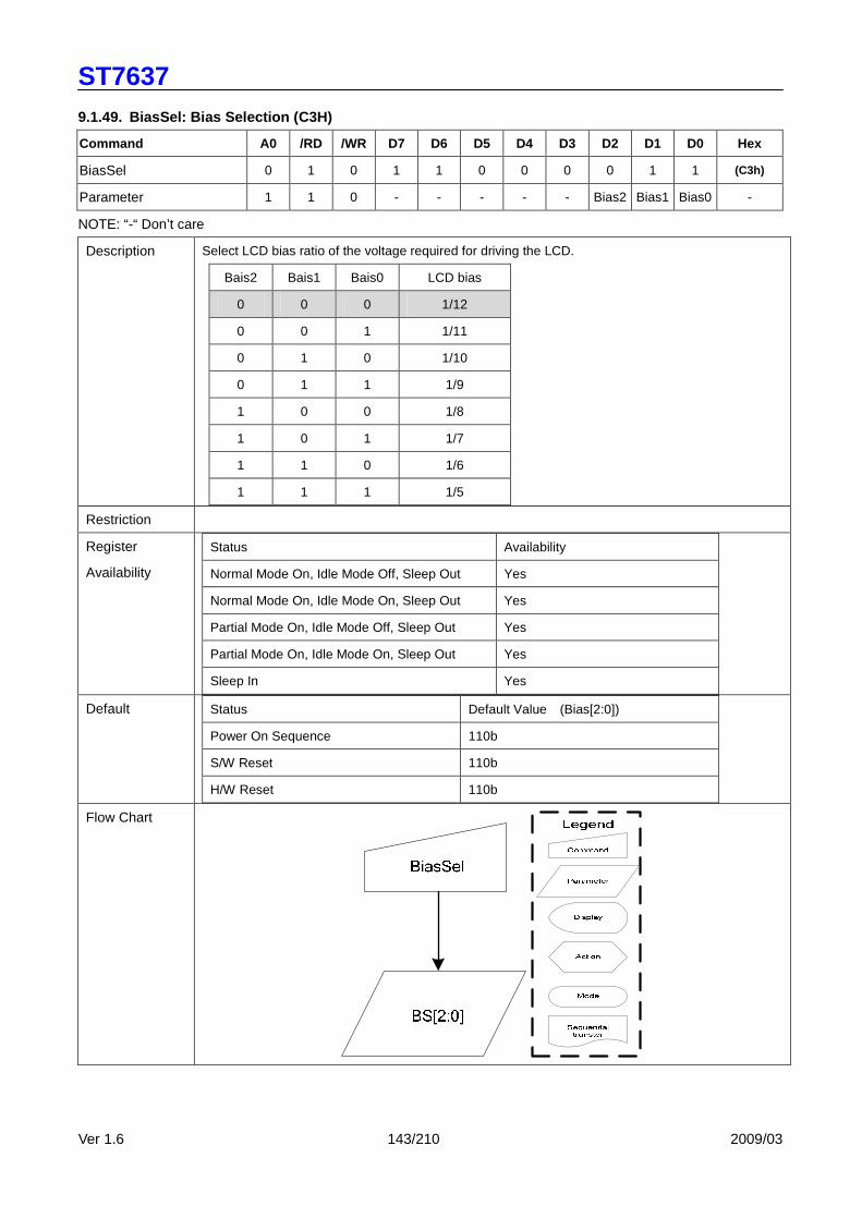
ST7637
Ver 1.6 143/210 2009/03
9.1.49. BiasSel: Bias Selection (C3H)
Command A0 /RD /WR D7 D6 D5 D4 D3 D2 D1 D0 Hex
BiasSel 0 1 0 1 1 0 0 0 0 1 1 (C3h)
Parameter 1 1 0 - - - - - Bias2 Bias1 Bias0 -
NOTE: “-“ Don’t care
Description Select LCD bias ratio of the voltage required for driving the LCD.
Bais2 Bais1 Bais0 LCD bias
0 0 0 1/12
0 0 1 1/11
0 1 0 1/10
0 1 1 1/9
1 0 0 1/8
1 0 1 1/7
1 1 0 1/6
1 1 1 1/5
Restriction
Register
Availability
Status Availability
Normal Mode On, Idle Mode Off, Sleep Out Yes
Normal Mode On, Idle Mode On, Sleep Out Yes
Partial Mode On, Idle Mode Off, Sleep Out Yes
Partial Mode On, Idle Mode On, Sleep Out Yes
Sleep In Yes Default Status Default Value (Bias[2:0])
Power On Sequence 110b
S/W Reset 110b
H/W Reset 110b Flow Chart
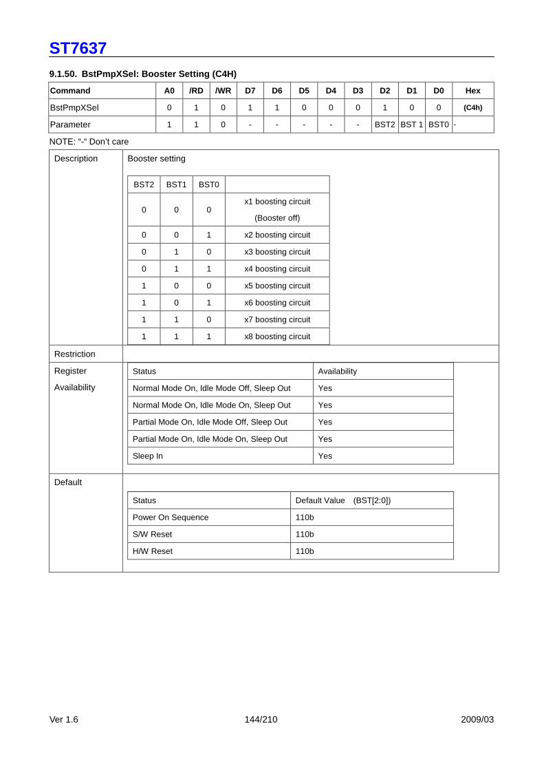
ST7637
Ver 1.6 144/210 2009/03
9.1.50. BstPmpXSel: Booster Setting (C4H)
Command A0 /RD /WR D7 D6 D5 D4 D3 D2 D1 D0 Hex
BstPmpXSel 0 1 0 1 1 0 0 0 1 0 0 (C4h)
Parameter 1 1 0 - - - - - BST2 BST 1 BST0 -
NOTE: “-“ Don’t care
Description Booster setting
BST2 BST1 BST0
0 0 0 x1 boosting circuit
(Booster off)
0 0 1 x2 boosting circuit
0 1 0 x3 boosting circuit
0 1 1 x4 boosting circuit
1 0 0 x5 boosting circuit
1 0 1 x6 boosting circuit
1 1 0 x7 boosting circuit
1 1 1 x8 boosting circuit
Restriction
Register
Availability
Status Availability
Normal Mode On, Idle Mode Off, Sleep Out Yes
Normal Mode On, Idle Mode On, Sleep Out Yes
Partial Mode On, Idle Mode Off, Sleep Out Yes
Partial Mode On, Idle Mode On, Sleep Out Yes
Sleep In Yes
Default
Status Default Value (BST[2:0])
Power On Sequence 110b
S/W Reset 110b
H/W Reset 110b
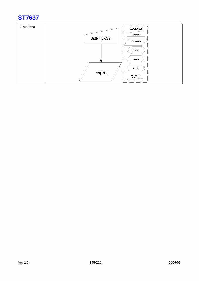
ST7637
Ver 1.6 145/210 2009/03
Flow Chart

ST7637
Ver 1.6 146/210 2009/03
9.1.51. BstEffSel: Booster Efficiency selection (C5 H)
Command A0 /RD /WR D7 D6 D5 D4 D3 D2 D1 D0 Hex
BstEffSel 0 1 0 1 1 0 0 0 1 0 1 (C5h)
Parameter 1 1 0 - - - - - - BTF1 BTF0 -
NOTE: “-“ Don’t care
Description Booster Efficiency set
BTF1 BTF0 Frequency ( Hz )
0 0 Level 1
0 1 Level 2 (default)
1 0 Level 3
By Booster Stages (2X, 3X, 4X, 5X, 6X, 7X, 8X) and Booster Efficiency (Level1~3) commands, we
could easily set the best Booster performance with suitable current consumption. If the Booster
Efficiency is set to higher level (level3 is higher than level1). The Boost Efficiency is better than lower
level, and it just need few more power consumption current.
Restriction
Register
Availability
Status Availability
Normal Mode On, Idle Mode Off, Sleep Out Yes
Normal Mode On, Idle Mode On, Sleep Out Yes
Partial Mode On, Idle Mode Off, Sleep Out Yes
Partial Mode On, Idle Mode On, Sleep Out Yes
Sleep In Yes
Default
Status Default Value (BTF[1:0])
Power On Sequence 01b
S/W Reset 01b
H/W Reset 01b

ST7637
Ver 1.6 147/210 2009/03
Flow Chart

ST7637
Ver 1.6 148/210 2009/03
9.1.52. VopOffset: Vop offset fuse bit adjust (C7H)
Command A0 /RD /WR D7 D6 D5 D4 D3 D2 D1 D0 Hex
VopOffset 0 1 0 1 1 0 0 0 1 1 1 (C7h)
Parameter1 1 1 0 VOS7 VOS6 VOS5 VOS4 VOS3 VOS2 VOS1 VOS0 -
Parameter2 1 1 0 - - - - - - - VOS8 -
NOTE: “-“ Don’t care
Description The command is used to the Vop offset for V0.
Restriction
Register
Availability
Status Availability
Normal Mode On, Idle Mode Off, Sleep Out Yes
Normal Mode On, Idle Mode On, Sleep Out Yes
Partial Mode On, Idle Mode Off, Sleep Out Yes
Partial Mode On, Idle Mode On, Sleep Out Yes
Sleep In Yes Default Status Default Value
VOS8 VOS[7:0]
Power On Sequence 0 0
S/W Reset 0 0
H/W Reset 0 0 Flow Chart

ST7637
Ver 1.6 149/210 2009/03
9.1.53. VgSorcSel: Vg source control (CBH)
Command A0 /RD /WR D7 D6 D5 D4 D3 D2 D1 D0 Hex
V3SorcSel 0 1 0 1 1 0 0 1 0 1 1 (CBh)
Parameter 1 1 0 - - - - - - - 2BT0 -
NOTE: “-“ Don’t care
Description 2BT0=0: Vg source comes from VDD2 ;
2BT0=1: Vg source comes from 2-times charge pump.
Restriction
Register
Availability
Status Availability
Normal Mode On, Idle Mode Off, Sleep Out Yes
Normal Mode On, Idle Mode On, Sleep Out Yes
Partial Mode On, Idle Mode Off, Sleep Out Yes
Partial Mode On, Idle Mode On, Sleep Out Yes
Sleep In Yes Default Status Default Value (2BT0)
Power On Sequence 1
S/W Reset 1
H/W Reset 1 Flow Chart

ST7637
Ver 1.6 150/210 2009/03
9.1.54. ID1Set : ID1 setting (CCH)
Command A0 /RD /WR D7 D6 D5 D4 D3 D2 D1 D0 Hex
ID1Set 0 1 0 1 1 0 0 1 1 0 0 (CCh)
Parameter 1 1 0 ID1_7 ID1_6 ID1_5 ID1_4 ID1_3 ID1_2 ID1_1 ID1_0 -
NOTE: “-“ Don’t care
Description ID1 setting for OTP program data input
Restriction
Register
Availability
Status Availability
Normal Mode On, Idle Mode Off, Sleep Out Yes
Normal Mode On, Idle Mode On, Sleep Out Yes
Partial Mode On, Idle Mode Off, Sleep Out Yes
Partial Mode On, Idle Mode On, Sleep Out Yes
Sleep In Yes Default Status Default Value
Power On Sequence 00h
S/W Reset 00h
H/W Reset 00h Flow Chart
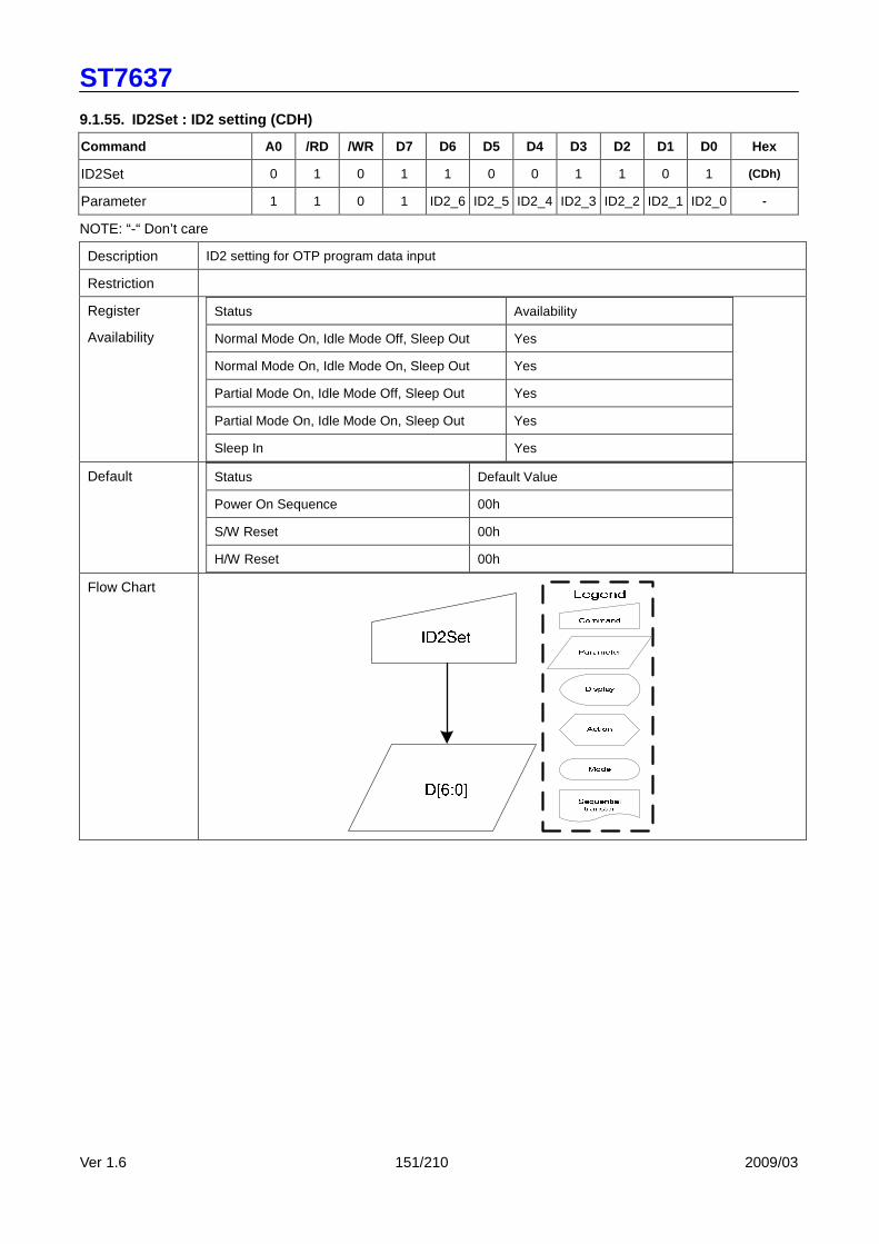
ST7637
Ver 1.6 151/210 2009/03
9.1.55. ID2Set : ID2 setting (CDH)
Command A0 /RD /WR D7 D6 D5 D4 D3 D2 D1 D0 Hex
ID2Set 0 1 0 1 1 0 0 1 1 0 1 (CDh)
Parameter 1 1 0 1 ID2_6 ID2_5 ID2_4 ID2_3 ID2_2 ID2_1 ID2_0 -
NOTE: “-“ Don’t care
Description ID2 setting for OTP program data input
Restriction
Register
Availability
Status Availability
Normal Mode On, Idle Mode Off, Sleep Out Yes
Normal Mode On, Idle Mode On, Sleep Out Yes
Partial Mode On, Idle Mode Off, Sleep Out Yes
Partial Mode On, Idle Mode On, Sleep Out Yes
Sleep In Yes Default Status Default Value
Power On Sequence 00h
S/W Reset 00h
H/W Reset 00h Flow Chart

ST7637
Ver 1.6 152/210 2009/03
9.1.56. ID3Set : ID3 setting (CEH)
Command A0 /RD /WR D7 D6 D5 D4 D3 D2 D1 D0 Hex
ID3Set 0 1 0 1 1 0 0 1 1 1 0 (CEh)
Parameter 1 1 0 ID3_7 ID3_6 ID3_5 ID3_4 ID3_3 ID3_2 ID3_1 ID3_0 -
NOTE: “-“ Don’t care
Description ID3 setting for OTP program data input
Restriction
Register
Availability
Status Availability
Normal Mode On, Idle Mode Off, Sleep Out Yes
Normal Mode On, Idle Mode On, Sleep Out Yes
Partial Mode On, Idle Mode Off, Sleep Out Yes
Partial Mode On, Idle Mode On, Sleep Out Yes
Sleep In Yes Default Status Default Value
Power On Sequence 00h
S/W Reset 00h
H/W Reset 00h Flow Chart
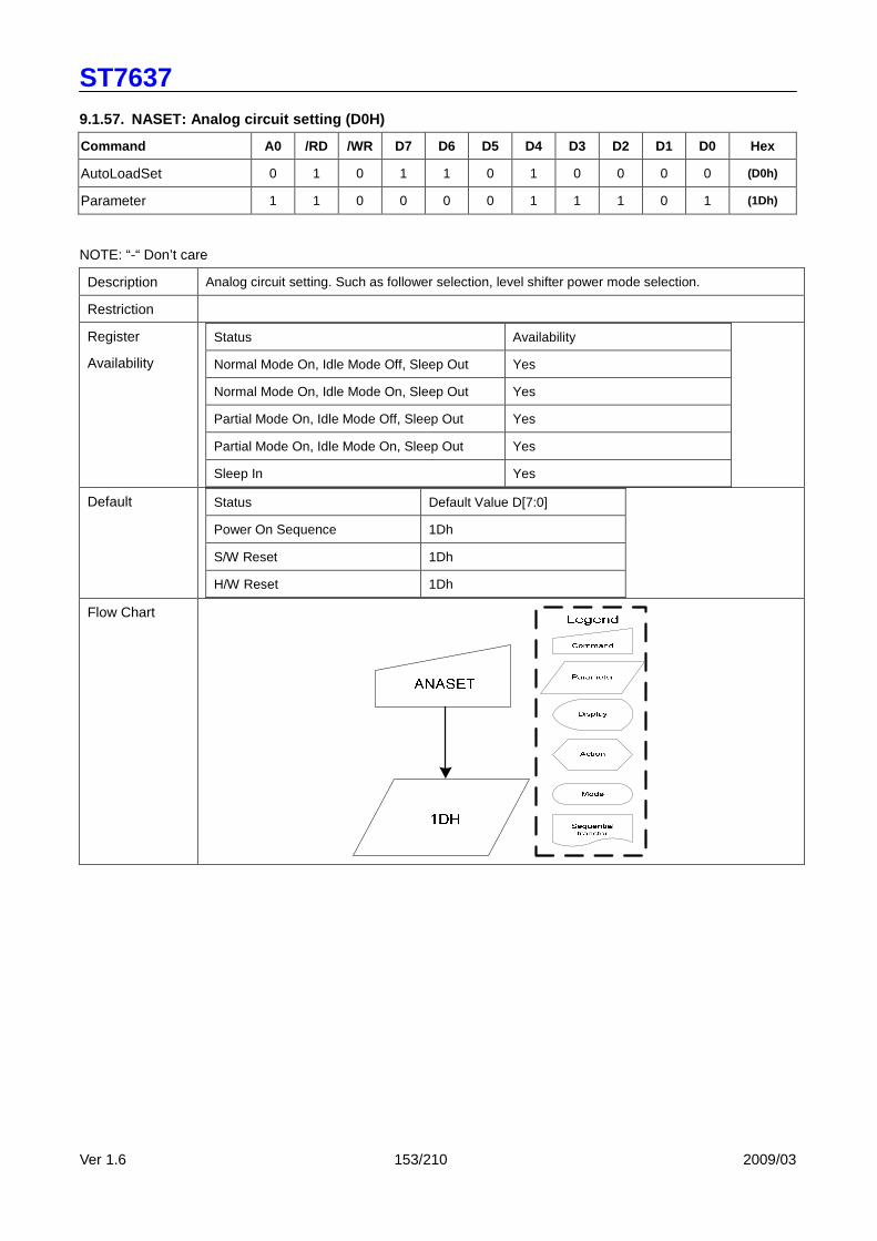
ST7637
Ver 1.6 153/210 2009/03
9.1.57. NASET: Analog circuit setting (D0H)
Command A0 /RD /WR D7 D6 D5 D4 D3 D2 D1 D0 Hex
AutoLoadSet 0 1 0 1 1 0 1 0 0 0 0 (D0h)
Parameter 1 1 0 0 0 0 1 1 1 0 1 (1Dh)
NOTE: “-“ Don’t care
Description Analog circuit setting. Such as follower selection, level shifter power mode selection.
Restriction
Register
Availability
Status Availability
Normal Mode On, Idle Mode Off, Sleep Out Yes
Normal Mode On, Idle Mode On, Sleep Out Yes
Partial Mode On, Idle Mode Off, Sleep Out Yes
Partial Mode On, Idle Mode On, Sleep Out Yes
Sleep In Yes Default Status Default Value D[7:0]
Power On Sequence 1Dh
S/W Reset 1Dh
H/W Reset 1Dh Flow Chart

ST7637
Ver 1.6 154/210 2009/03
9.1.58. AutoLoadSet: mask rom data auto re-load con trol (D7H)
Command A0 /RD /WR D7 D6 D5 D4 D3 D2 D1 D0 Hex
AutoLoadSet 0 1 0 1 1 0 1 0 1 1 1 (D7h)
Parameter 1 1 0 EXTE OTPBE - ARD 1 1 1 1 -
NOTE: “-“ Don’t care
Description Mask rom data auto re-load control
EXTE : External command enable (OTP input), 1: enable, 0: disable
OTPBE: OTPB auto-read enable (OTP input, force disable when ARD=0)
ARD : OTP auto recovery enable control, 1: Disable OTP auto recovery,
0: Enable OTP auto recovery
Restriction
Register
Availability
Status Availability
Normal Mode On, Idle Mode Off, Sleep Out Yes
Normal Mode On, Idle Mode On, Sleep Out Yes
Partial Mode On, Idle Mode Off, Sleep Out Yes
Partial Mode On, Idle Mode On, Sleep Out Yes
Sleep In Yes
Default Status Default ValueD[7:0]
Power On Sequence 00h
S/W Reset 00h
H/W Reset 00h
Flow Chart

ST7637
Ver 1.6 155/210 2009/03
9.1.59. RDTstStatus: Read IC status (DEH)
Command A0 /RD /WR D7 D6 D5 D4 D3 D2 D1 D0 Hex
RDTstStatus 0 1 0 1 1 0 1 1 1 1 0 (DEh)
Dummy Read 1 0 1 - - - - - - - -
Parameter 1 0 1 RD7 RD6 RD5 RD4 RD3 RD2 RD1 RD0 -
NOTE: “-“ Don’t care
Description Read IC status.
Contect of OTP / RDA / PWR_VOP read control
(selection Byte by StusOutByteSel[3:0] control)
Restriction
Register
Availability
Status Availability
Normal Mode On, Idle Mode Off, Sleep Out Yes
Normal Mode On, Idle Mode On, Sleep Out Yes
Partial Mode On, Idle Mode Off, Sleep Out Yes
Partial Mode On, Idle Mode On, Sleep Out Yes
Sleep In Yes Default Status Default Value
Power On Sequence -
S/W Reset -
H/W Reset - Flow Chart

ST7637
Ver 1.6 156/210 2009/03
9.1.60. EPCTIN: Control OTP WR/XRD (E0H)
Command A0 /RD /WR D7 D6 D5 D4 D3 D2 D1 D0 Hex
EPCTIN 0 1 0 1 1 1 0 0 0 0 0 (E0h)
Parameter 1 1 0 0 0
WR
/XRD
0 0 0 0 0 -
NOTE: “-“ Don’t care
Description WR/XRD: when setting “1” The Write Enable of OTP will be opened.
WR/XRD: when setting “0” The Read Enable of OTP will be opened.
Restriction
Register
Availability
Status Availability
Normal Mode On, Idle Mode Off, Sleep Out Yes
Normal Mode On, Idle Mode On, Sleep Out Yes
Partial Mode On, Idle Mode Off, Sleep Out Yes
Partial Mode On, Idle Mode On, Sleep Out Yes
Sleep In Yes Default Status Default Value (WR/XRD)
Power On Sequence 0
S/W Reset 0
H/W Reset 0 Flow Chart
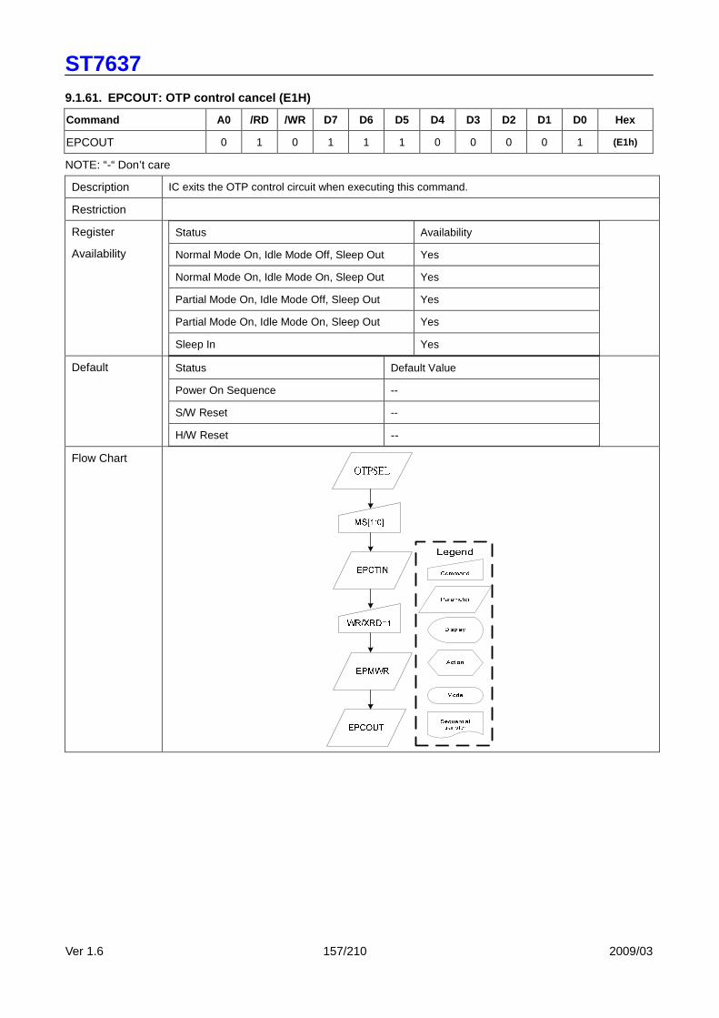
ST7637
Ver 1.6 157/210 2009/03
9.1.61. EPCOUT: OTP control cancel (E1H)
Command A0 /RD /WR D7 D6 D5 D4 D3 D2 D1 D0 Hex
EPCOUT 0 1 0 1 1 1 0 0 0 0 1 (E1h)
NOTE: “-“ Don’t care
Description IC exits the OTP control circuit when executing this command.
Restriction
Register
Availability
Status Availability
Normal Mode On, Idle Mode Off, Sleep Out Yes
Normal Mode On, Idle Mode On, Sleep Out Yes
Partial Mode On, Idle Mode Off, Sleep Out Yes
Partial Mode On, Idle Mode On, Sleep Out Yes
Sleep In Yes Default Status Default Value
Power On Sequence --
S/W Reset --
H/W Reset -- Flow Chart
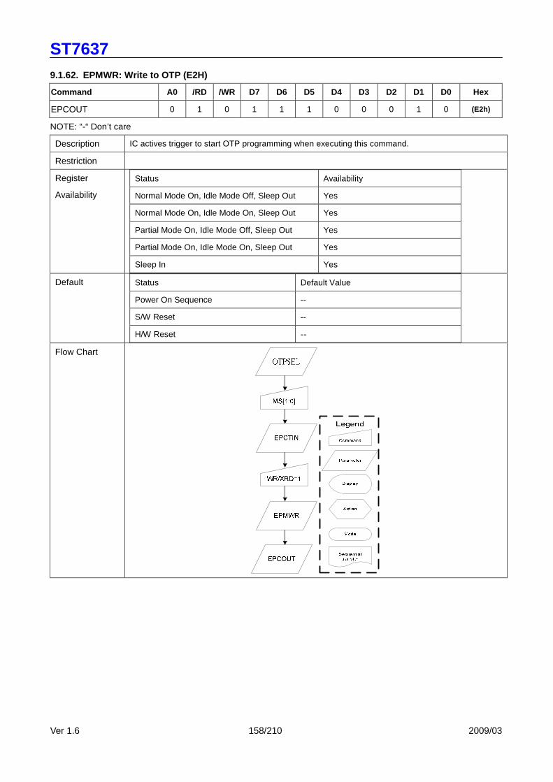
ST7637
Ver 1.6 158/210 2009/03
9.1.62. EPMWR: Write to OTP (E2H)
Command A0 /RD /WR D7 D6 D5 D4 D3 D2 D1 D0 Hex
EPCOUT 0 1 0 1 1 1 0 0 0 1 0 (E2h)
NOTE: “-“ Don’t care
Description IC actives trigger to start OTP programming when executing this command.
Restriction
Register
Availability
Status Availability
Normal Mode On, Idle Mode Off, Sleep Out Yes
Normal Mode On, Idle Mode On, Sleep Out Yes
Partial Mode On, Idle Mode Off, Sleep Out Yes
Partial Mode On, Idle Mode On, Sleep Out Yes
Sleep In Yes Default Status Default Value
Power On Sequence --
S/W Reset --
H/W Reset -- Flow Chart
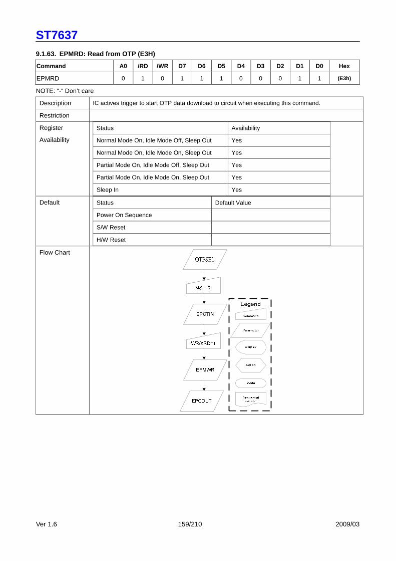
ST7637
Ver 1.6 159/210 2009/03
9.1.63. EPMRD: Read from OTP (E3H)
Command A0 /RD /WR D7 D6 D5 D4 D3 D2 D1 D0 Hex
EPMRD 0 1 0 1 1 1 0 0 0 1 1 (E3h)
NOTE: “-“ Don’t care
Description IC actives trigger to start OTP data download to circuit when executing this command.
Restriction
Register
Availability
Status Availability
Normal Mode On, Idle Mode Off, Sleep Out Yes
Normal Mode On, Idle Mode On, Sleep Out Yes
Partial Mode On, Idle Mode Off, Sleep Out Yes
Partial Mode On, Idle Mode On, Sleep Out Yes
Sleep In Yes Default Status Default Value
Power On Sequence
S/W Reset
H/W Reset Flow Chart
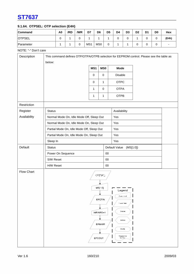
ST7637
Ver 1.6 160/210 2009/03
9.1.64. OTPSEL: OTP selection (E4H)
Command A0 /RD /WR D7 D6 D5 D4 D3 D2 D1 D0 Hex
OTPSEL 0 1 0 1 1 1 0 0 1 0 0 (E4h)
Parameter 1 1 0 MS1 MS0 0 1 1 0 0 0 -
NOTE: “-“ Don’t care
Description This command defines OTP/OTPA/OTPB selection for EEPROM control. Please see the table as
below:
MS1 MS0 Mode
0 0 Disable
0 1 OTPC
1 0 OTPA
1 1 OTPB
Restriction
Register
Availability
Status Availability
Normal Mode On, Idle Mode Off, Sleep Out Yes
Normal Mode On, Idle Mode On, Sleep Out Yes
Partial Mode On, Idle Mode Off, Sleep Out Yes
Partial Mode On, Idle Mode On, Sleep Out Yes
Sleep In Yes Default Status Default Value (MS[1:0])
Power On Sequence 00
S/W Reset 00
H/W Reset 00 Flow Chart
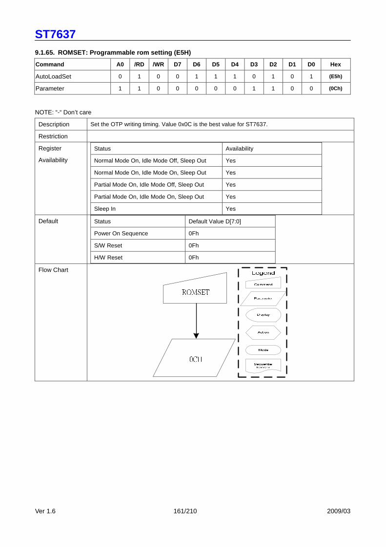
ST7637
Ver 1.6 161/210 2009/03
9.1.65. ROMSET: Programmable rom setting (E5H)
Command A0 /RD /WR D7 D6 D5 D4 D3 D2 D1 D0 Hex
AutoLoadSet 0 1 0 0 1 1 1 0 1 0 1 (E5h)
Parameter 1 1 0 0 0 0 0 1 1 0 0 (0Ch)
NOTE: “-“ Don’t care
Description Set the OTP writing timing. Value 0x0C is the best value for ST7637.
Restriction
Register
Availability
Status Availability
Normal Mode On, Idle Mode Off, Sleep Out Yes
Normal Mode On, Idle Mode On, Sleep Out Yes
Partial Mode On, Idle Mode Off, Sleep Out Yes
Partial Mode On, Idle Mode On, Sleep Out Yes
Sleep In Yes Default Status Default Value D[7:0]
Power On Sequence 0Fh
S/W Reset 0Fh
H/W Reset 0Fh Flow Chart
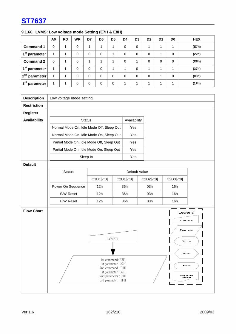
ST7637
Ver 1.6 162/210 2009/03
9.1.66. LVMS: Low voltage mode Setting (E7H & E8H)
A0 RD WR D7 D6 D5 D4 D3 D2 D1 D0 HEX
Command 1 0 1 0 1 1 1 0 0 1 1 1 (E7h)
1st parameter 1 1 0 0 0 1 0 0 0 1 0 (22h)
Command 2 0 1 0 1 1 1 0 1 0 0 0 (E8h)
1st parameter 1 1 0 0 0 1 1 0 1 1 1 (37h)
2nd parameter 1 1 0 0 0 0 0 0 0 1 0 (03h)
3rd parameter 1 1 0 0 0 0 1 1 1 1 1 (1Fh)
Description Low voltage mode setting.
Restriction
Register
Availability
Status Availability
Normal Mode On, Idle Mode Off, Sleep Out Yes
Normal Mode On, Idle Mode On, Sleep Out Yes
Partial Mode On, Idle Mode Off, Sleep Out Yes
Partial Mode On, Idle Mode On, Sleep Out Yes
Sleep In Yes
Default
Default Value Status
C1D1[7:0] C2D1[7:0] C2D2[7:0] C2D3[7:0]
Power On Sequence 12h 36h 03h 16h
S/W Reset 12h 36h 03h 16h
H/W Reset 12h 36h 03h 16h
Flow Chart
1st command: E7H1st parameter : 22H2nd command : E8H1st parameter : 37H2nd parameter : 03H3rd parameter : 1FH
LVMSEL

ST7637
Ver 1.6 163/210 2009/03
9.1.67. HPMSET : High Power Mode Setting (EBH)
A0 RD WR D7 D6 D5 D4 D3 D2 D1 D0 HEX
Command 0 1 0 1 1 1 0 1 0 1 1 (Ebh)
1st parameter 1 1 0 0 0 0 0 0 0 1 0 (02h)
2nd parameter 1 1 0 0 0 0 0 0 0 0 1 (01h)
Description High power mode for volatage compensation.
Restriction
Register
Availability
Status Availability
Normal Mode On, Idle Mode Off, Sleep Out Yes
Normal Mode On, Idle Mode On, Sleep Out Yes
Partial Mode On, Idle Mode Off, Sleep Out Yes
Partial Mode On, Idle Mode On, Sleep Out Yes
Sleep In Yes
Default
Default Value Status
HP[3:0]
Power On Sequence 00h
S/W Reset 00h
H/W Reset 00h
Flow Chart
1st parameter : 02H2nd parameter : 01H
HPMSEL

ST7637
Ver 1.6 164/210 2009/03
9.1.68. FRMSEL: Frame Freq. in Temperature range (F 0H)
A0 RD WR D7 D6 D5 D4 D3 D2 D1 D0 HEX
Command 0 1 0 1 1 1 1 0 0 0 0 (F0H)
1st parameter 1 1 0 - - - DIVA FA3 FA2 FA1 FA0 Range A
2nd parameter 1 1 0 - - - DIVB FB3 FB2 FB1 FB0 Range B
3rd parameter 1 1 0 - - - DIVC FC3 FC2 FC1 FC0 Range C
4th parameter 1 1 0 - - - DIVD FD3 FD2 FD1 FD0 Range D
Description Select Frame Freq. in normal display mode.
1st parameter : Frame freq. value set in temperature range 30(-30 ) to TA
2nd parameter : Frame freq. value set in temperature P range TA to TB
3rd parameter : Frame freq. value set in temperature range TB to TC
4th parameter : Frame freq. value set in temperature range TC to 145(90 )
For command setting to frame rate value look-up-table, please see the following table:
DIVx Fx[3:0] Frame Rate
(Hz)
0 75
1 76
2 77
3 80
4 84
5 88
6 92
7 97
8 102
9 108
A 115
B 123
C 133
D 144
E 155
1
F 170
0 0~F (Frame Rate) / 2
Restriction

ST7637
Ver 1.6 165/210 2009/03
Register
Availability
Status Availability
Normal Mode On, Idle Mode Off, Sleep Out Yes
Normal Mode On, Idle Mode On, Sleep Out Yes
Partial Mode On, Idle Mode Off, Sleep Out Yes
Partial Mode On, Idle Mode On, Sleep Out Yes
Sleep In Yes
Default
Default Value Status
FA[4:0] FB[4:0] FC[4:0] FD[4:0]
Power On Sequence 06h 0Bh 0Dh 12h
S/W Reset 06h 0Bh 0Dh 12h
H/W Reset 06h 0Bh 0Dh 12h
Flow Chart
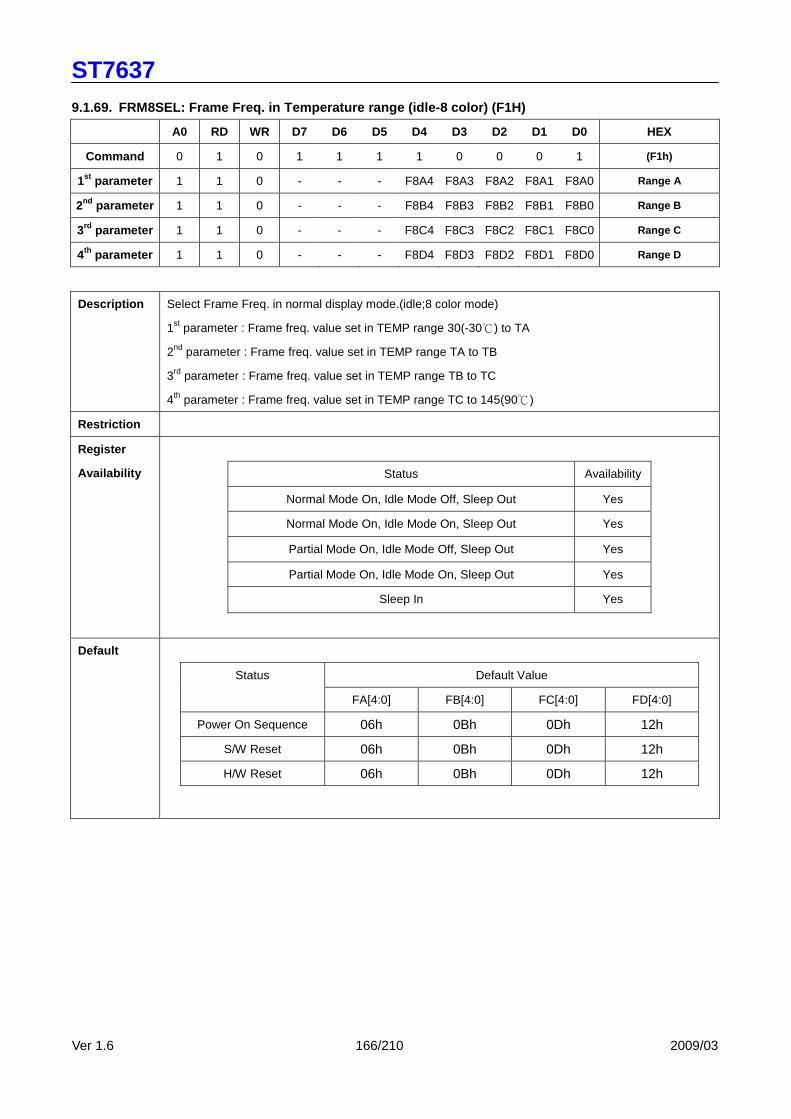
ST7637
Ver 1.6 166/210 2009/03
9.1.69. FRM8SEL: Frame Freq. in Temperature range ( idle-8 color) (F1H)
A0 RD WR D7 D6 D5 D4 D3 D2 D1 D0 HEX
Command 0 1 0 1 1 1 1 0 0 0 1 (F1h)
1st parameter 1 1 0 - - - F8A4 F8A3 F8A2 F8A1 F8A0 Range A
2nd parameter 1 1 0 - - - F8B4 F8B3 F8B2 F8B1 F8B0 Range B
3rd parameter 1 1 0 - - - F8C4 F8C3 F8C2 F8C1 F8C0 Range C
4th parameter 1 1 0 - - - F8D4 F8D3 F8D2 F8D1 F8D0 Range D
Description Select Frame Freq. in normal display mode.(idle;8 color mode)
1st parameter : Frame freq. value set in TEMP range 30(-30 ) to TA
2nd parameter : Frame freq. value set in TEMP range TA to TB
3rd parameter : Frame freq. value set in TEMP range TB to TC
4th parameter : Frame freq. value set in TEMP range TC to 145(90 )
Restriction
Register
Availability
Status Availability
Normal Mode On, Idle Mode Off, Sleep Out Yes
Normal Mode On, Idle Mode On, Sleep Out Yes
Partial Mode On, Idle Mode Off, Sleep Out Yes
Partial Mode On, Idle Mode On, Sleep Out Yes
Sleep In Yes
Default
Default Value Status
FA[4:0] FB[4:0] FC[4:0] FD[4:0]
Power On Sequence 06h 0Bh 0Dh 12h
S/W Reset 06h 0Bh 0Dh 12h
H/W Reset 06h 0Bh 0Dh 12h
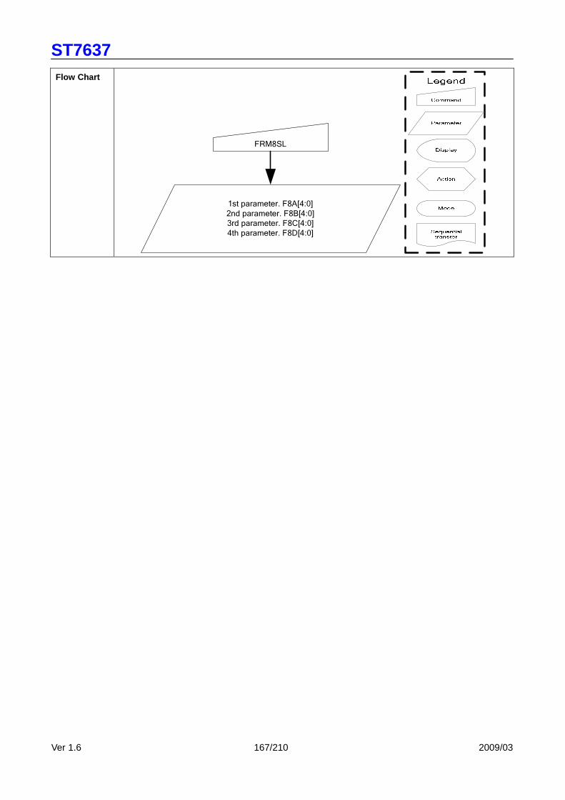
ST7637
Ver 1.6 167/210 2009/03
Flow Chart
1st parameter. F8A[4:0]
2nd parameter. F8B[4:0]3rd parameter. F8C[4:0]
4th parameter. F8D[4:0]
FRM8SL

ST7637
Ver 1.6 168/210 2009/03
9.1.70. TMPRNG: Temp. range set for Frame Freq. Adj . (F2H)
A0 RD WR D7 D6 D5 D4 D3 D2 D1 D0 HEX
Command 0 1 0 1 1 1 1 0 0 1 0 (F2h)
1st parameter 1 1 0 - TA6 TA5 TA4 TA3 TA2 TA1 TA0 Range A
2nd parameter 1 1 0 - TB6 TB5 TB4 TB3 TB2 TB1 TB0 Range B
3rd parameter 1 1 0 - TC6 TC5 TC4 TC3 TC2 TC1 TC0 Range C
Description Temp. range set for automatic frame freq. adj. operation according the current temp. value.
1st parameter: Temp. range A value set
2nd parameter: Temp. range B value set
3rd parameter: Temp. range C value set
TA/TB/TC Temperature( ) + 40 = TA/TB/TC[6 :0]
Example:
If TA wants to be set at 24, TA[6:0]=24+40=64(40h),
Restriction -40 TA TA+TH TB TB+TH TC 87
Register
Availability
Status Availability
Normal Mode On, Idle Mode Off, Sleep Out Yes
Normal Mode On, Idle Mode On, Sleep Out Yes
Partial Mode On, Idle Mode Off, Sleep Out Yes
Partial Mode On, Idle Mode On, Sleep Out Yes
Sleep In Yes
Default
Default Value Status
TA[6:0] TB[6:0] TC[6:0]
Power On Sequence 1Eh 28h 32h
S/W Reset 1Eh 28h 32h
H/W Reset 1Eh 28h 32h
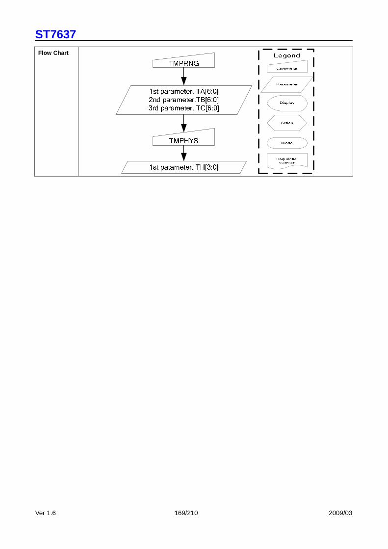
ST7637
Ver 1.6 169/210 2009/03
Flow Chart

ST7637
Ver 1.6 170/210 2009/03
9.1.71. TMPHYS: Temp. Hysteresis Set for Frame Freq . Adj. (F3H)
A0 RD WR D7 D6 D5 D4 D3 D2 D1 D0 HEX
Command 0 1 0 1 1 1 1 0 0 1 1 (F3h)
1st parameter 1 1 0 - - - - TH3 TH2 TH1 TH0
Description Temp. hysteresis range set for frame freq. adj.
Parameter TH[3:0] is used to set Temp. hysteresis range.
The relationship between temp. state and temp. range value is shown below.
TEMP Range Value TEMP Rising State TEMP Falling State
Freq. changing point A TA[6:0]+TH[3:0] TA[6:0]
Freq. changing point B TB[6:0]+TH[3:0] TB[6:0]
Freq. changing point C TC[6:0]+TH[3:0] TC[6:0]
TH Temperature( ) – 1 = TH[3:0]
Example:
If TH wants to set 5 , TH[3:0]=5 -1=4.
Restriction Temp. hysteresis value should be smaller than the gap of temp. range.
Register
Availability
Status Availability
Normal Mode On, Idle Mode Off, Sleep Out Yes
Normal Mode On, Idle Mode On, Sleep Out Yes
Partial Mode On, Idle Mode Off, Sleep Out Yes
Partial Mode On, Idle Mode On, Sleep Out Yes
Sleep In Yes
Default
Status Default Value(TH[3:0])
Power On Sequence 04h
S/W Reset 04h
H/W Reset 04h
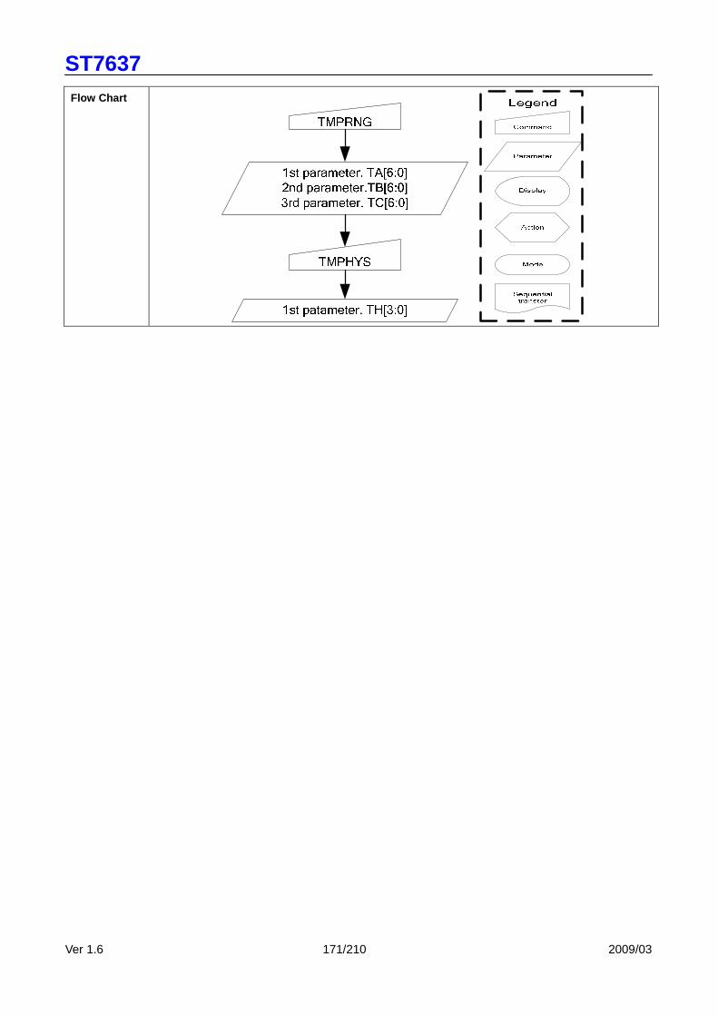
ST7637
Ver 1.6 171/210 2009/03
Flow Chart
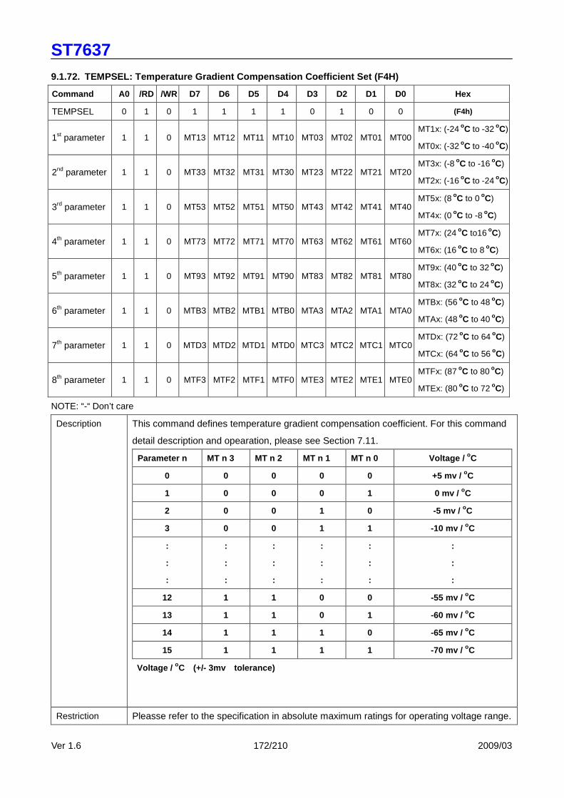
ST7637
Ver 1.6 172/210 2009/03
9.1.72. TEMPSEL: Temperature Gradient Compensation Coefficient Set (F4H)
Command A0 /RD /WR D7 D6 D5 D4 D3 D2 D1 D0 Hex
TEMPSEL 0 1 0 1 1 1 1 0 1 0 0 (F4h)
1st parameter 1 1 0 MT13 MT12 MT11 MT10 MT03 MT02 MT01 MT00 MT1x: (-24 oC to -32 oC)
MT0x: (-32 oC to -40 oC)
2nd parameter 1 1 0 MT33 MT32 MT31 MT30 MT23 MT22 MT21 MT20 MT3x: (-8 oC to -16 oC)
MT2x: (-16 oC to -24 oC)
3rd parameter 1 1 0 MT53 MT52 MT51 MT50 MT43 MT42 MT41 MT40 MT5x: (8 oC to 0 oC)
MT4x: (0 oC to -8 oC)
4th parameter 1 1 0 MT73 MT72 MT71 MT70 MT63 MT62 MT61 MT60 MT7x: (24 oC to16 oC)
MT6x: (16 oC to 8 oC)
5th parameter 1 1 0 MT93 MT92 MT91 MT90 MT83 MT82 MT81 MT80 MT9x: (40 oC to 32 oC)
MT8x: (32 oC to 24 oC)
6th parameter 1 1 0 MTB3 MTB2 MTB1 MTB0 MTA3 MTA2 MTA1 MTA0 MTBx: (56 oC to 48 oC)
MTAx: (48 oC to 40 oC)
7th parameter 1 1 0 MTD3 MTD2 MTD1 MTD0 MTC3 MTC2 MTC1 MTC0 MTDx: (72 oC to 64 oC)
MTCx: (64 oC to 56 oC)
8th parameter 1 1 0 MTF3 MTF2 MTF1 MTF0 MTE3 MTE2 MTE1 MTE0 MTFx: (87 oC to 80 oC)
MTEx: (80 oC to 72 oC)
NOTE: “-“ Don’t care
Description This command defines temperature gradient compensation coefficient. For this command
detail description and opearation, please see Section 7.11.
Parameter n MT n 3 MT n 2 MT n 1 MT n 0 Voltage / oC
0 0 0 0 0 +5 mv / oC
1 0 0 0 1 0 mv / oC
2 0 0 1 0 -5 mv / oC
3 0 0 1 1 -10 mv / oC
:
:
:
:
:
:
:
:
:
:
:
:
:
:
:
:
:
:
12 1 1 0 0 -55 mv / oC
13 1 1 0 1 -60 mv / oC
14 1 1 1 0 -65 mv / oC
15 1 1 1 1 -70 mv / oC
Voltage / oC (+/- 3mv tolerance)
Restriction Pleasse refer to the specification in absolute maximum ratings for operating voltage range.

ST7637
Ver 1.6 173/210 2009/03
Register
Availability
Status Availability
Normal Mode On, Idle Mode Off, Sleep Out Yes
Normal Mode On, Idle Mode On, Sleep Out Yes
Partial Mode On, Idle Mode Off, Sleep Out Yes
Partial Mode On, Idle Mode On, Sleep Out Yes
Sleep In Yes Default Status Default Value (MTn[3:0])
Power On Sequence
S/W Reset
H/W Reset
1st parameter 0xFF
2nd parameter 0x36
3rd parameter 0x04
4th parameter 0x00
5th parameter 0x33
6th parameter 0x42
7th parameter 0xC4
8th parameter 0x59 Flow Chart
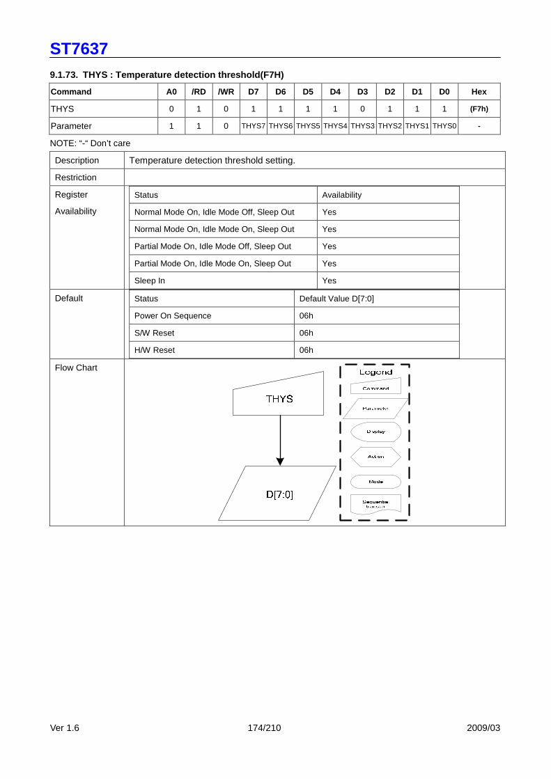
ST7637
Ver 1.6 174/210 2009/03
9.1.73. THYS : Temperature detection threshold(F7H)
Command A0 /RD /WR D7 D6 D5 D4 D3 D2 D1 D0 Hex
THYS 0 1 0 1 1 1 1 0 1 1 1 (F7h)
Parameter 1 1 0 THYS7 THYS6 THYS5 THYS4 THYS3 THYS2 THYS1 THYS0 -
NOTE: “-“ Don’t care
Description Temperature detection threshold setting.
Restriction
Register
Availability
Status Availability
Normal Mode On, Idle Mode Off, Sleep Out Yes
Normal Mode On, Idle Mode On, Sleep Out Yes
Partial Mode On, Idle Mode Off, Sleep Out Yes
Partial Mode On, Idle Mode On, Sleep Out Yes
Sleep In Yes Default Status Default Value D[7:0]
Power On Sequence 06h
S/W Reset 06h
H/W Reset 06h Flow Chart

ST7637
Ver 1.6 175/210 2009/03
9.1.74. Frame Set: Frame PWM Set (F9H)
Command A0 /RD /WR D7 D6 D5 D4 D3 D2 D1 D0 Hex
Frame1 Set 0 1 0 1 1 1 1 1 0 0 1 (F9h)
1st parameter 1 1 0 - - - P14 P13 P12 P11 P10 -
2nd parameter 1 1 0 - - - P24 P23 P22 P21 P20 -
: : : : : : : : : : : : -
15th parameter 1 1 0 - - - P154 P153 P152 P151 P150 -
16th parameter 1 1 0 - - - P164 P163 P162 P161 P160 -
NOTE: “-“ Don’t care
Description This command is used to set frame PWM.
Restriction
Register
Availability
Status Availability
Normal Mode On, Idle Mode Off, Sleep Out Yes
Normal Mode On, Idle Mode On, Sleep Out Yes
Partial Mode On, Idle Mode Off, Sleep Out Yes
Partial Mode On, Idle Mode On, Sleep Out Yes
Sleep In Yes Default Status Default Value
Power On Sequence --
S/W Reset --
H/W Reset -- Flow Chart
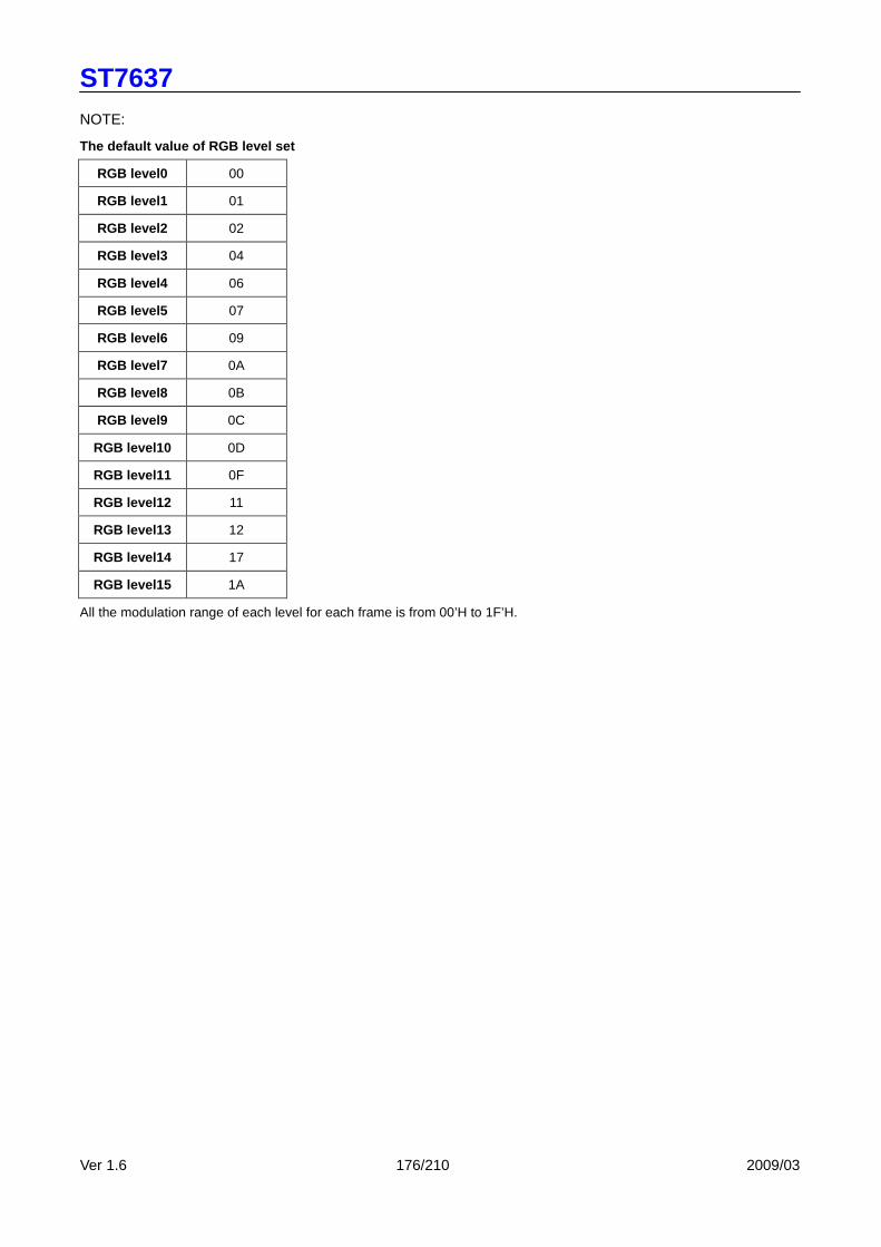
ST7637
Ver 1.6 176/210 2009/03
NOTE:
The default value of RGB level set
RGB level0 00
RGB level1 01
RGB level2 02
RGB level3 04
RGB level4 06
RGB level5 07
RGB level6 09
RGB level7 0A
RGB level8 0B
RGB level9 0C
RGB level10 0D
RGB level11 0F
RGB level12 11
RGB level13 12
RGB level14 17
RGB level15 1A
All the modulation range of each level for each frame is from 00’H to 1F’H.

ST7637
Ver 1.6 177/210 2009/03
10. SPECIFICATIONS 10.1 ABSOLUTE MAXIMUM RATINGS
(VSS = 0V)
Item Symbol Value Unit
Supply voltage 1 VDD,VDD1 - 0.3 ~ + 3.0 V
Supply voltage 2 VDD2,VDD3,VDD4,VDD5 - 0.3 ~ + 4.2 V
Supply voltage 3 VMAX (V0- XV0) - 0.3 ~ + 18.0 V
Input voltage range VIN - 0.3 ~ VDD + 0.3 V
Operating temperature range TOPR - 30 ~ + 85 °C
Storage temperature range TSTG - 40 ~ + 125 °C
NOTE:
(1). Voltages are all based on VSS = 0V.
(2). Voltage relationship: V0≧Vg≧Vm≧VSS≧XV0 must always be satisfied.
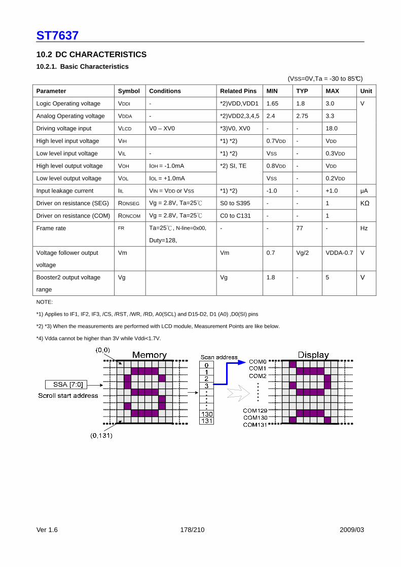
ST7637
Ver 1.6 178/210 2009/03
10.2 DC CHARACTERISTICS 10.2.1. Basic Characteristics
(VSS=0V,Ta = -30 to 85°C)
Parameter Symbol Conditions Related Pins MIN TYP MAX Unit
Logic Operating voltage VDDI - *2)VDD,VDD1 1.65 1.8 3.0
Analog Operating voltage VDDA - *2)VDD2,3,4,5 2.4 2.75 3.3
Driving voltage input VLCD V0 – XV0 *3)V0, XV0 - - 18.0
High level input voltage VIH *1) *2) 0.7VDD - VDD
Low level input voltage VIL - *1) *2) VSS - 0.3VDD
High level output voltage VOH IOH = -1.0mA 0.8VDD - VDD
Low level output voltage VOL IOL = +1.0mA
*2) SI, TE
VSS - 0.2VDD
V
Input leakage current IIL VIN = VDD or VSS *1) *2) -1.0 - +1.0 µA
Driver on resistance (SEG) RONSEG Vg = 2.8V, Ta=25 S0 to S395 - - 1
Driver on resistance (COM) RONCOM Vg = 2.8V, Ta=25 C0 to C131 - - 1
KΩ
Frame rate FR Ta=25, N-line=0x00,
Duty=128,
- - 77 - Hz
Voltage follower output
voltage
Vm Vm 0.7 Vg/2 VDDA-0.7 V
Booster2 output voltage
range
Vg Vg 1.8 - 5 V
NOTE:
*1) Applies to IF1, IF2, IF3, /CS, /RST, /WR, /RD, A0(SCL) and D15-D2, D1 (A0) ,D0(SI) pins
*2) *3) When the measurements are performed with LCD module, Measurement Points are like below.
*4) Vdda cannot be higher than 3V while Vddi<1.7V.

ST7637
Ver 1.6 179/210 2009/03
10.2.2. Current Consumption
Current consumption
Typical Maximum Operation mode Condition
IDD (mA) IDD (mA)
- Normal Mode
1. 1/2 gray pattern
2. Vddi=1.8V, Vdda=2.8V
2. Vop=12V, bias=1/9. N=0x00,
FR=77Hz, x8 booster, Ta=25
0.6 0.9
- Sleep In Mode Vddi=1.8V, Vdda=2.8V, Ta=25 0.01 0.018
Note:
The Current Consumption is DC characteristics.
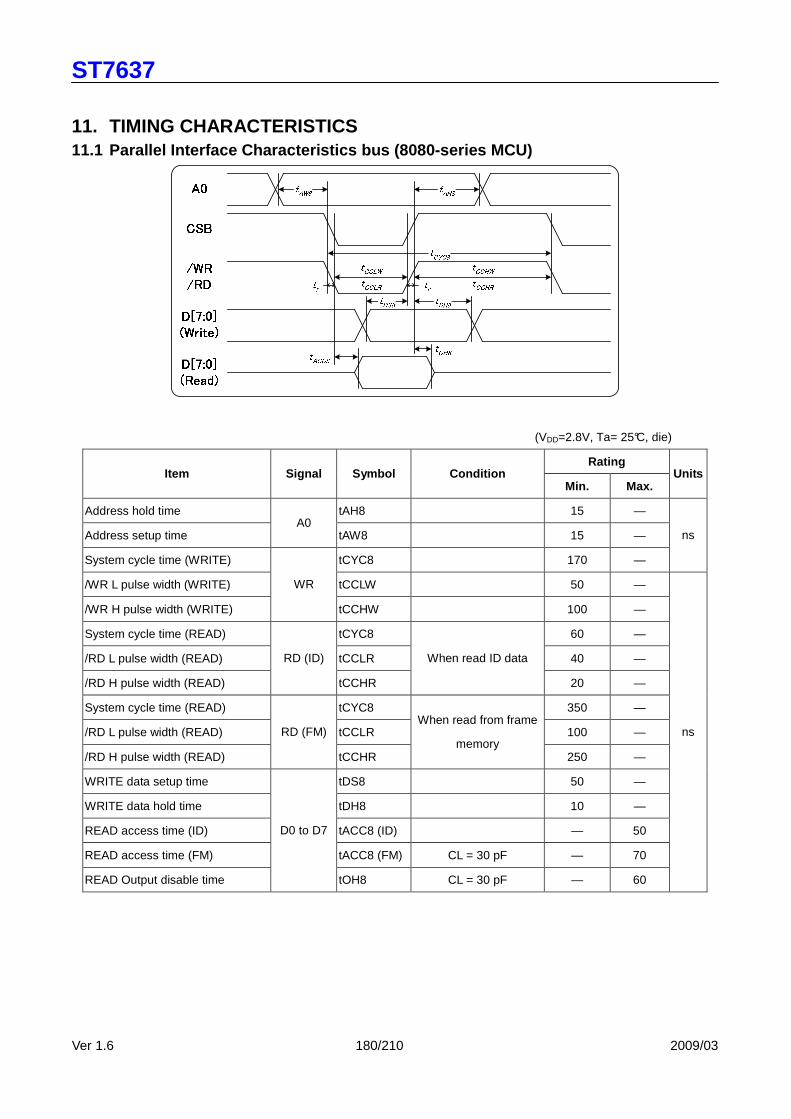
ST7637
Ver 1.6 180/210 2009/03
11. TIMING CHARACTERISTICS 11.1 Parallel Interface Characteristics bus (8080-s eries MCU)
(VDD=2.8V, Ta= 25°C, die)
Rating Item Signal Symbol Condition
Min. Max. Units
Address hold time tAH8 15 —
Address setup time A0
tAW8 15 —
System cycle time (WRITE) tCYC8 170 —
ns
/WR L pulse width (WRITE) tCCLW 50 —
/WR H pulse width (WRITE)
WR
tCCHW 100 —
System cycle time (READ) tCYC8 60 —
/RD L pulse width (READ) tCCLR 40 —
/RD H pulse width (READ)
RD (ID)
tCCHR
When read ID data
20 —
System cycle time (READ) tCYC8 350 —
/RD L pulse width (READ) tCCLR 100 —
/RD H pulse width (READ)
RD (FM)
tCCHR
When read from frame
memory 250 —
WRITE data setup time tDS8 50 —
WRITE data hold time tDH8 10 —
READ access time (ID) tACC8 (ID) — 50
READ access time (FM) tACC8 (FM) CL = 30 pF — 70
READ Output disable time
D0 to D7
tOH8 CL = 30 pF — 60
ns

ST7637
Ver 1.6 181/210 2009/03
(VDD=1.8V, Ta= 25°C, die)
Rating Item Signal Symbol Condition
Min. Max. Units
Address hold time tAH8 15 —
Address setup time A0
tAW8 15 —
System cycle time (WRITE) tCYC8 260 —
ns
/WR L pulse width (WRITE) tCCLW 80 —
/WR H pulse width (WRITE)
WR
tCCHW 170 —
System cycle time (READ) tCYC8 110 —
/RD L pulse width (READ) tCCLR 70 —
/RD H pulse width (READ)
RD (ID)
tCCHR
When read ID data
25 —
System cycle time (READ) tCYC8 450 —
/RD L pulse width (READ) tCCLR 140 —
/RD H pulse width (READ)
RD (FM)
tCCHR
When read from frame
memory 300 —
WRITE data setup time tDS8 60 —
WRITE data hold time tDH8 10 —
READ access time (ID) tACC8 (ID) — 60
READ access time (FM) tACC8 (FM) CL = 30 pF — 90
READ Output disable time
D0 to D7
tOH8 CL = 30 pF — 80
ns
*1 The input signal rise time and fall time (tr, tf) is specified at 15 ns or less. When the system cycle time is extremely fast,
(tr +tf) (tCYC8 – tCCLW – tCCHW) for (tr + tf) (tCYC8 – tCCLR – tCCHR) are specified.
*2 All timing is specified using 20% and 80% of VDD as the reference.
*3 tCCLW and tCCLR are specified as the overlap between /CS being “L” and WR and RD being at the “L” level.

ST7637
Ver 1.6 182/210 2009/03
11.2 Parallel Interface Characteristics bus (6800-s eries MCU)
(VDD=2.8V, Ta= 25°C, die)
Rating Item Signal Symbol Condition
Min. Max. Units
Address hold time tAH8 10 —
Address setup time A0
tAW8 10 —
System cycle time (WRITE) tCYC8 130 —
ns
/WR L pulse width (WRITE) tCCLW 85 —
/WR H pulse width (WRITE)
E
tCCHW 45 —
System cycle time (READ) tCYC8 65 —
/RD L pulse width (READ) tCCLR 15 —
/RD H pulse width (READ)
RD (ID)
tCCHR
When read ID data
35 —
System cycle time (READ) tCYC8 250 —
/RD L pulse width (READ) tCCLR 130 —
/RD H pulse width (READ)
RD (FM)
tCCHR
When read from frame
memory 120 —
WRITE data setup time tDS8 50 —
WRITE data hold time tDH8 10 —
READ access time (ID) tACC8 (ID) — 70
READ access time (FM) tACC8 (FM) CL = 30 pF — 70
READ Output disable time
D0 to D7
tOH8 CL = 30 pF — 60
ns
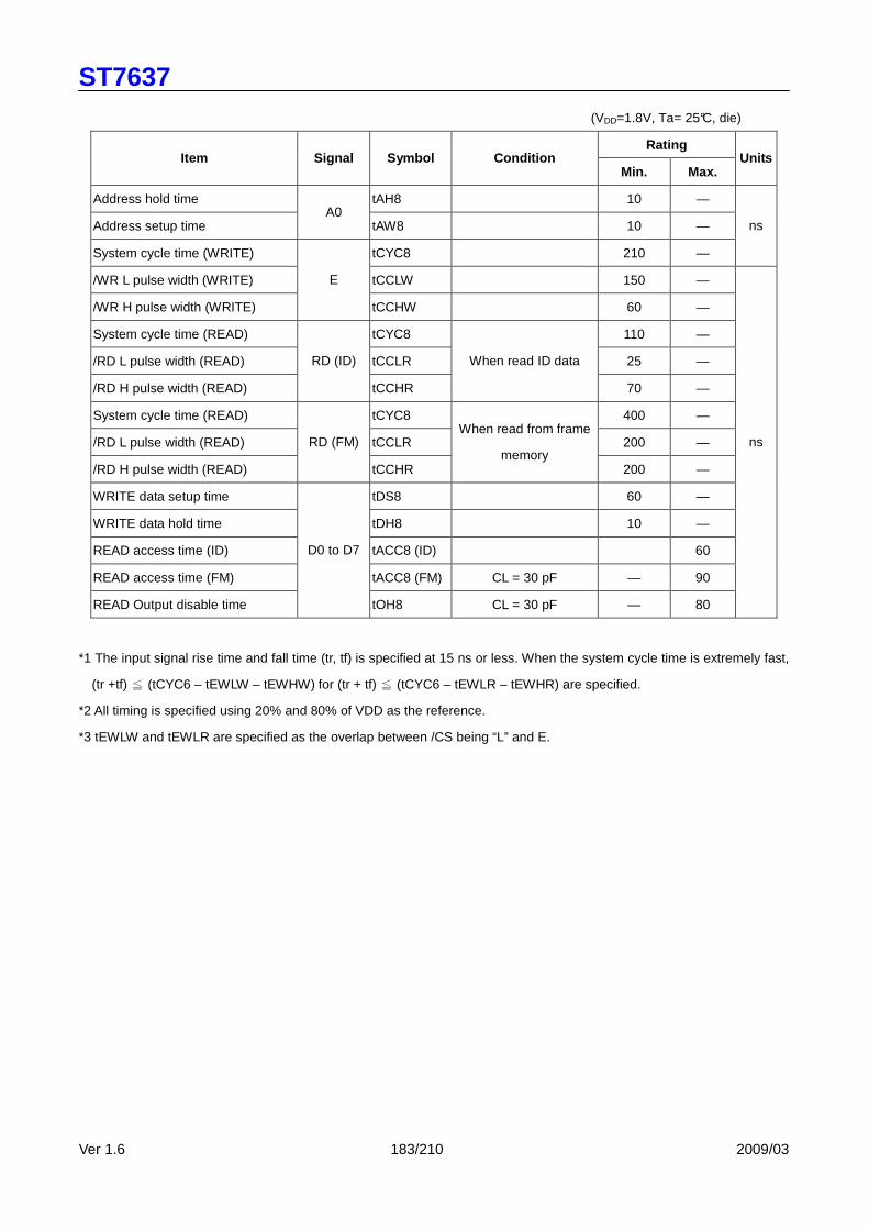
ST7637
Ver 1.6 183/210 2009/03
(VDD=1.8V, Ta= 25°C, die)
Rating Item Signal Symbol Condition
Min. Max. Units
Address hold time tAH8 10 —
Address setup time A0
tAW8 10 —
System cycle time (WRITE) tCYC8 210 —
ns
/WR L pulse width (WRITE) tCCLW 150 —
/WR H pulse width (WRITE)
E
tCCHW 60 —
System cycle time (READ) tCYC8 110 —
/RD L pulse width (READ) tCCLR 25 —
/RD H pulse width (READ)
RD (ID)
tCCHR
When read ID data
70 —
System cycle time (READ) tCYC8 400 —
/RD L pulse width (READ) tCCLR 200 —
/RD H pulse width (READ)
RD (FM)
tCCHR
When read from frame
memory 200 —
WRITE data setup time tDS8 60 —
WRITE data hold time tDH8 10 —
READ access time (ID) tACC8 (ID) 60
READ access time (FM) tACC8 (FM) CL = 30 pF — 90
READ Output disable time
D0 to D7
tOH8 CL = 30 pF — 80
ns
*1 The input signal rise time and fall time (tr, tf) is specified at 15 ns or less. When the system cycle time is extremely fast,
(tr +tf) (tCYC6 – tEWLW – tEWHW) for (tr + tf) (tCYC6 – tEWLR – tEWHR) are specified.
*2 All timing is specified using 20% and 80% of VDD as the reference.
*3 tEWLW and tEWLR are specified as the overlap between /CS being “L” and E.

ST7637
Ver 1.6 184/210 2009/03
11.3 Serial Interface Characteristics (4-pin Serial )
/CS
SCL
SI
(DIN)
SI
(DOUT)
VIH
VIH
VIH
VIH
VIL
VIL
VIL
VIL
TCSS TSCYCW /TSCYCRTCSH
TCHW
TSCCTSLW /TSLR
TSHW /TSHR
TSDS TSDH
TACC TOH
TSAS TSAH
A0
(VDD=2.8V, Ta= 25°C, die)
Rating Item Signal Symbol Condition
Min. Max. Units
Serial clock period (write) tSCYCW 60 —
SCL “H” pulse width (write) tSHW 30 —
SCL “L” pulse width (write) tSLW 30 —
Serial clock period (read) tSCYCR 130 —
SCL “H” pulse width (read) tSHR 65 —
SCL “L” pulse width (read)
SCL
tSLR 65 —
Address setup time tSAS 10 —
Address hold time A0
tSAH 20 —
Data setup time tSDS 10 —
Data hold time tSDH 20 —
Data access time tACC CL=30pF — 50
Output disable time
SI
tOH CL=30pF — 50
Chip select setup time tCSS 30 —
Chip select hold time tCSH 30 —
Chip select "H" pulse width
/CS
tCHW 0 —
ns
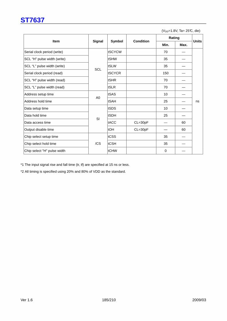
ST7637
Ver 1.6 185/210 2009/03
(VDD=1.8V, Ta= 25°C, die)
Rating Item Signal Symbol Condition
Min. Max. Units
Serial clock period (write) tSCYCW 70 —
SCL “H” pulse width (write) tSHW 35 —
SCL “L” pulse width (write) tSLW 35 —
Serial clock period (read) tSCYCR 150 —
SCL “H” pulse width (read) tSHR 70 —
SCL “L” pulse width (read)
SCL
tSLR 70 —
Address setup time tSAS 10 —
Address hold time A0
tSAH 25 —
Data setup time tSDS 10 —
Data hold time tSDH 25 —
Data access time tACC CL=30pF — 60
Output disable time
SI
tOH CL=30pF — 60
Chip select setup time tCSS 35 —
Chip select hold time tCSH 35 —
Chip select "H" pulse width
/CS
tCHW 0 —
ns
*1 The input signal rise and fall time (tr, tf) are specified at 15 ns or less.
*2 All timing is specified using 20% and 80% of VDD as the standard.
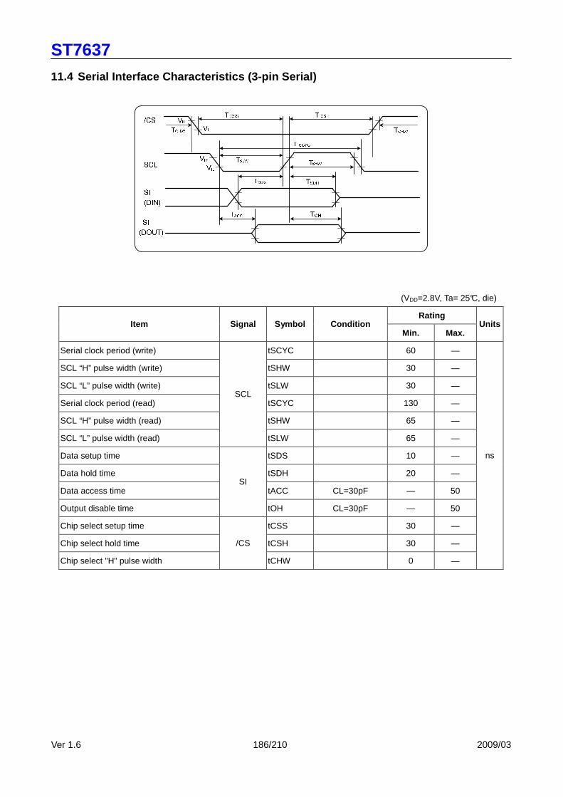
ST7637
Ver 1.6 186/210 2009/03
11.4 Serial Interface Characteristics (3-pin Serial )
(VDD=2.8V, Ta= 25°C, die)
Rating Item Signal Symbol Condition
Min. Max. Units
Serial clock period (write) tSCYC 60 —
SCL “H” pulse width (write) tSHW 30 —
SCL “L” pulse width (write) tSLW 30 —
Serial clock period (read) tSCYC 130 —
SCL “H” pulse width (read) tSHW 65 —
SCL “L” pulse width (read)
SCL
tSLW 65 —
Data setup time tSDS 10 —
Data hold time tSDH 20 —
Data access time tACC CL=30pF — 50
Output disable time
SI
tOH CL=30pF — 50
Chip select setup time tCSS 30 —
Chip select hold time tCSH 30 —
Chip select "H" pulse width
/CS
tCHW 0 —
ns
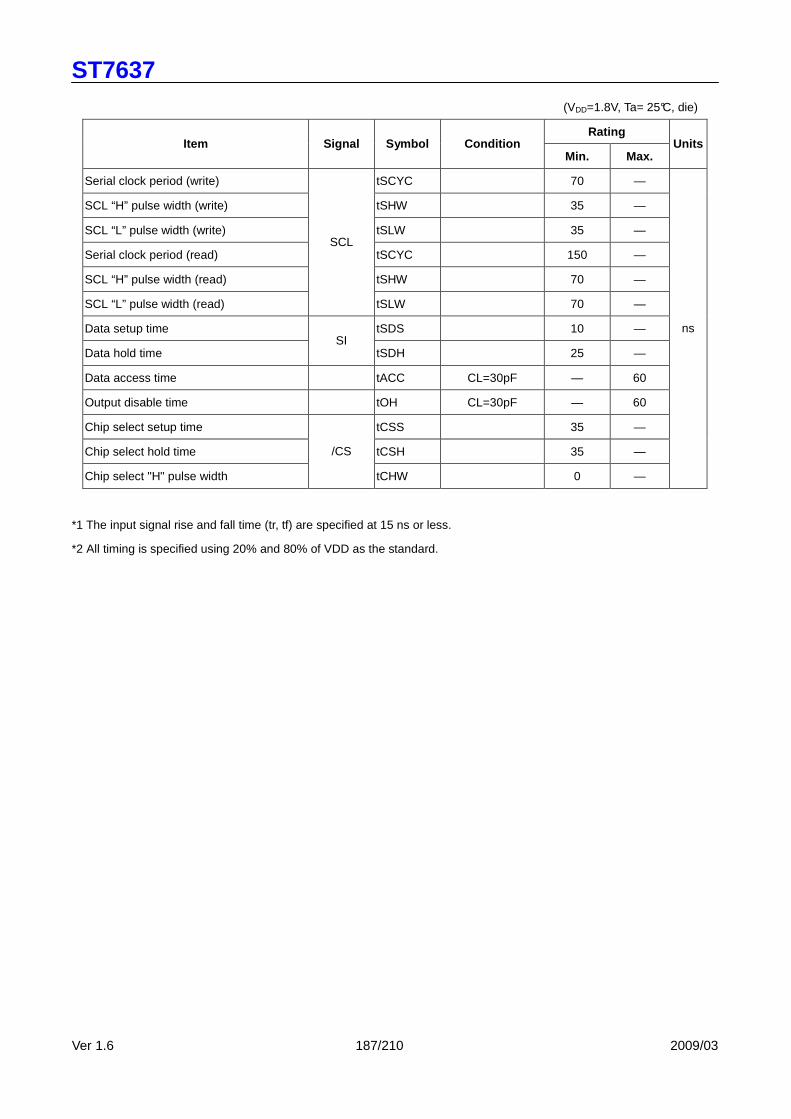
ST7637
Ver 1.6 187/210 2009/03
(VDD=1.8V, Ta= 25°C, die)
Rating Item Signal Symbol Condition
Min. Max. Units
Serial clock period (write) tSCYC 70 —
SCL “H” pulse width (write) tSHW 35 —
SCL “L” pulse width (write) tSLW 35 —
Serial clock period (read) tSCYC 150 —
SCL “H” pulse width (read) tSHW 70 —
SCL “L” pulse width (read)
SCL
tSLW 70 —
Data setup time tSDS 10 —
Data hold time SI
tSDH 25 —
Data access time tACC CL=30pF — 60
Output disable time tOH CL=30pF — 60
Chip select setup time tCSS 35 —
Chip select hold time tCSH 35 —
Chip select "H" pulse width
/CS
tCHW 0 —
ns
*1 The input signal rise and fall time (tr, tf) are specified at 15 ns or less.
*2 All timing is specified using 20% and 80% of VDD as the standard.

ST7637
Ver 1.6 188/210 2009/03
11.5 Ouput access/disable timing measurement method Parallel interface (8080-series)
Serial interface (3-line)
Note:
1. pull-up/pull-down resistor: 3KΩ ± 5% ; pull-up/pull-down capacitor: 8 or 30 pF ± 10%
2. Capacitances and resistances of the oscilloscope’s probe must be included externals components in these
measurements.

ST7637
Ver 1.6 189/210 2009/03
11.5.1.1. Minimum value measurement
Parallel interface (8080-series)
Serial interface (3-line)
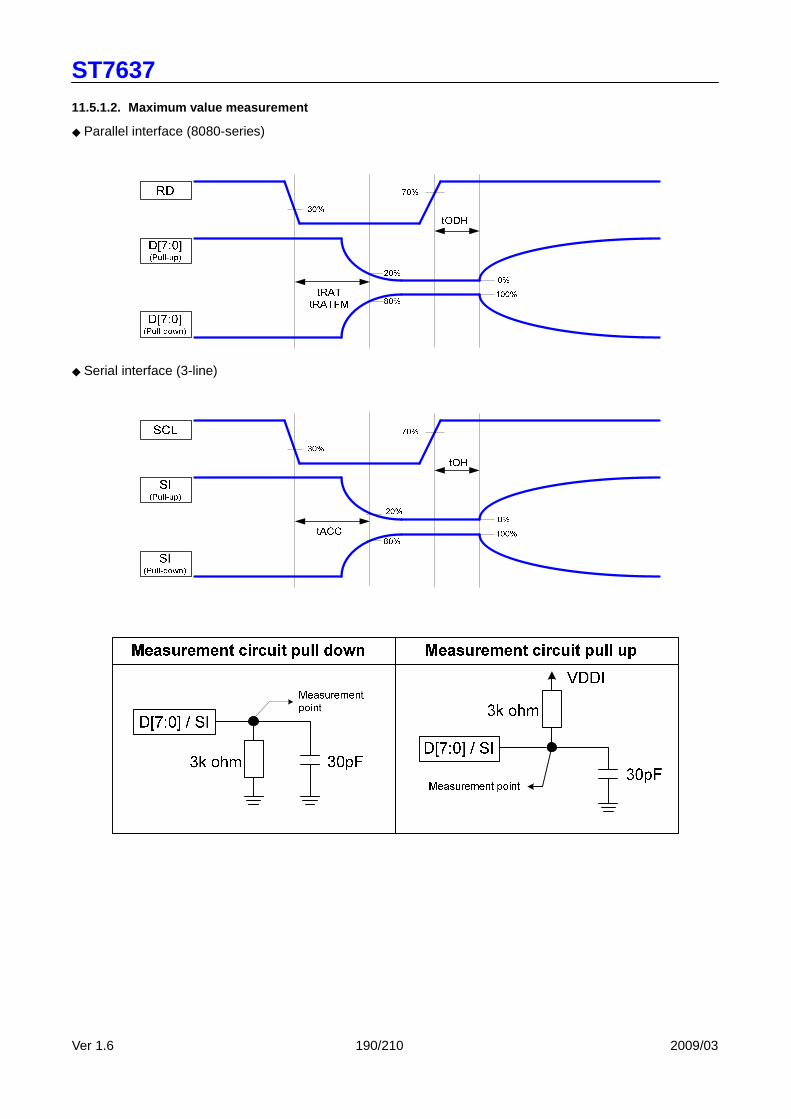
ST7637
Ver 1.6 190/210 2009/03
11.5.1.2. Maximum value measurement
Parallel interface (8080-series)
Serial interface (3-line)
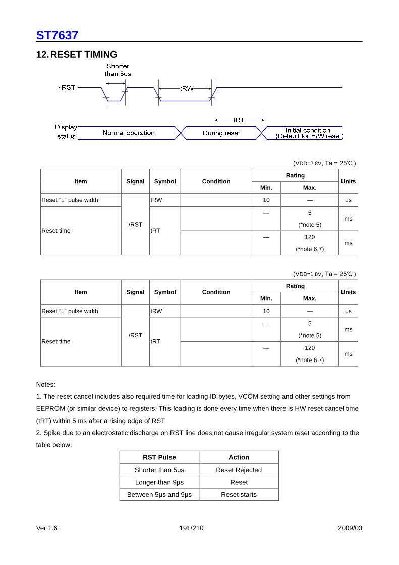
ST7637
Ver 1.6 191/210 2009/03
12. RESET TIMING
(VDD=2.8V, Ta = 25°C )
Rating Item Signal Symbol Condition
Min. Max. Units
Reset “L” pulse width tRW 10 — us
— 5
(*note 5) ms
Reset time /RST
tRT
— 120
(*note 6,7) ms
(VDD=1.8V, Ta = 25°C )
Rating Item Signal Symbol Condition
Min. Max. Units
Reset “L” pulse width tRW 10 — us
— 5
(*note 5) ms
Reset time /RST
tRT
— 120
(*note 6,7) ms
Notes:
1. The reset cancel includes also required time for loading ID bytes, VCOM setting and other settings from
EEPROM (or similar device) to registers. This loading is done every time when there is HW reset cancel time
(tRT) within 5 ms after a rising edge of RST
2. Spike due to an electrostatic discharge on RST line does not cause irregular system reset according to the
table below:
RST Pulse Action
Shorter than 5µs Reset Rejected
Longer than 9µs Reset
Between 5µs and 9µs Reset starts

ST7637
Ver 1.6 192/210 2009/03
3. During the Resetting period, the display will be blanked (The display is entering blanking sequence, which
maximum time is 120 ms, when Reset Starts in Sleep Out –mode. The display remains the blank state in Sleep
In –mode.) and then return to Default condition for Hardware Reset.
4. Spike Rejection also applies during a valid reset pulse as shown below:
5. When Reset applied during Sleep In Mode.
6. When Reset applied during Sleep Out Mode.
7. It is necessary to wait 5msec after releasing RST before sending commands. Also Sleep Out command
cannot be sent for 120msec.

ST7637
Ver 1.6 193/210 2009/03
13. THE MPU INTERFACE (REFERENCE EXAMPLES) The ST7637 Series can be connected to either 8080 Series MPUs or to 6800 Series MPUs. Moreover, using the serial
interface it is possible to operate the ST7637 series chips with fewer signal lines.
The display area can be enlarged by using multiple ST7637 Series chips. When this is done, the chip select signal can be
used to select the individual Ics to access.
(1) 8080 Series MPUs
MPU
ST7637
(2) 6800 Series MPUs
MPU
ST7637
(3) Using the Serial Interface (4-line interface)
MPU
ST7637
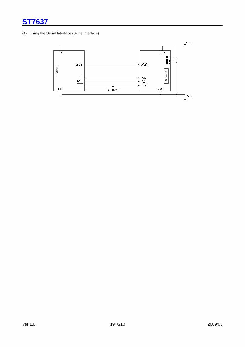
ST7637
Ver 1.6 194/210 2009/03
(4) Using the Serial Interface (3-line interface)
MPU
ST7637

ST7637
Ver 1.6 195/210 2009/03
A – Application Note A1a – 80 series 8-bit parallel interlace Mode
IF[3:1] HHL CLS H (internal OSC) CSEL H C1 1uF/16V C2 1uF/25V C3 1uF/16V

ST7637
Ver 1.6 196/210 2009/03
A1b – 80 series 16-bit parallel interlace Mode
IF[3:1] HHH CLS H (internal OSC) CSEL H C1 1uF/16V C2 1uF/25V C3 1uF/16V

ST7637
Ver 1.6 197/210 2009/03
A1c – 68 series 8-bit parallel interlace Mode
F[3:1] HLL CLS H (internal OSC) CSEL H C1 1uF/16V C2 1uF/25V C3 1uF/16V
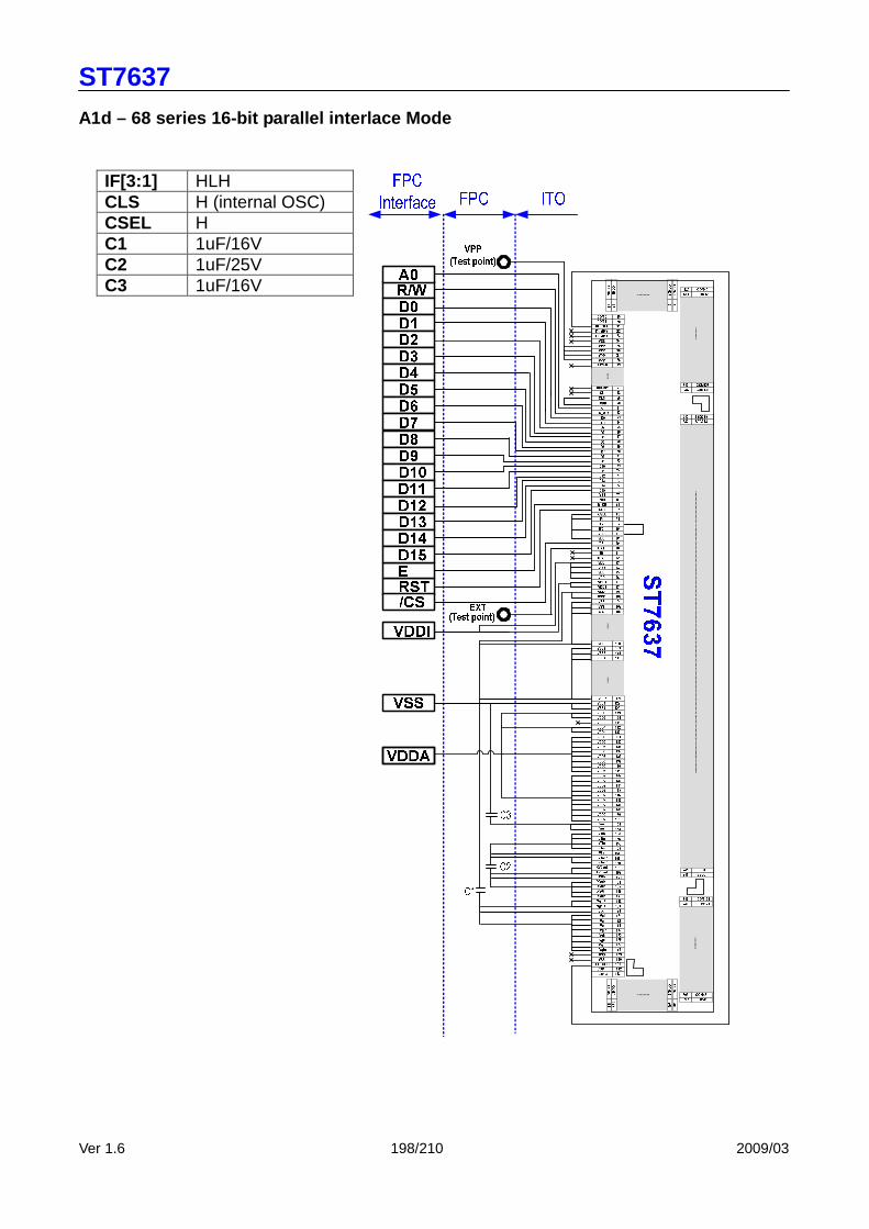
ST7637
Ver 1.6 198/210 2009/03
A1d – 68 series 16-bit parallel interlace Mode
IF[3:1] HLH CLS H (internal OSC) CSEL H C1 1uF/16V C2 1uF/25V C3 1uF/16V

ST7637
Ver 1.6 199/210 2009/03
A1e – 4-line serial interlace Mode
FPC
FPC
Interface ITO
SI
RST
/CSEXT
(Test point)
SCL
C1
VSS
VDDA
VDDI
C3
VPP
(Test point)
C2
A0
21
22
23
24VSS
25VPP
26VPP
27VPP
28VPP29DUMMY
57DUMMY
58CL
59CLS
60
61
62
VDD
63
A0
64
RW_WR
65
D0
66
D1
67
D2
68
D3
69
D4
70
D5
71
D6
72
D7
73
D8
74
D9
75
D10
76
D11
77
D12
78
D13
79
D14
80
D15
81E_RD
82RST
83CSEL
84IF1
85IF2
86IF3
87VSS
88VDD
89/CS
90/EXT
91TE
92TCAP
93VDD
94VDD
95VDD
96VDD
97VDD1
98VDD1
99VSS1
100VSS1
101VSS
108VSS
109
102VSS
103VSS
110VSS2
111VSS2
126VSS2
127VSS4
VSS4
VDD3
VDD3
VREF
VDD4
VDD4
VDD5
VDD5
VDD5
VDD5
VDD5
VDD5
VDD5
VDD5
VDD2
VDD2
VDD2
VDD2
VDD2VDD2
VDD2
VDD2
VDD2
VDD2
Vm
Vm
V0in
V0in
V0in
V0in
V0s
V0out
V0out
XV0out
XV0outXV0s
XV0inXV0in
XV0in
XV0in
Vgout
Vgin
Vgin
Vgin
128
129
130
131
132
133
134
135
136
137
138
139
140
141
142
143
144
145
146
147
148
149
150
151
152
153
154
155
156
157
158
159
160
161
162
163
164165
166
167
168
169170
172173
174
175176
177
178
1COM38
2
COM4
17COM6
689 COM40
688 COM42
645 COM128
644 COM130
643 SEG395
642 SEG394
249 SEG1
248 SEG0
ST7637
COM36
18
19
20
COM 2
COM 0
DETGBI
DUMMY
DUMMY
181
182
183
179
180VSS
DETGBO
COM 1
COM 3
VSS
247 COM131
246 COM129
203 COM43
202 COM41201COM39
200
COM5
185COM7
COM37
184
VSS
VDD
VSS2
Vgout
Vgs
Vgin
Vgin
Vgin
Vgin
Vgin 171
IF[3:1] LHH CLS H (internal OSC) CSEL H C1 1uF/16V C2 1uF/25V C3 1uF/16V
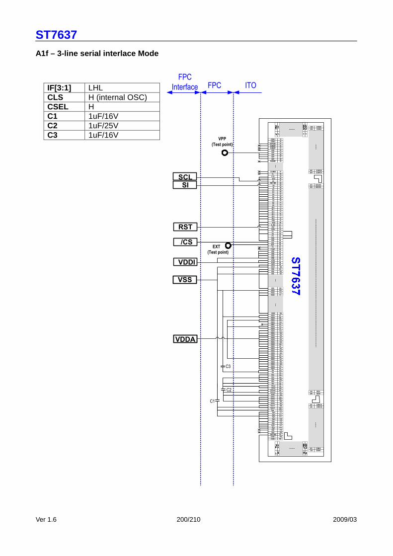
ST7637
Ver 1.6 200/210 2009/03
A1f – 3-line serial interlace Mode
21
22
23
24VSS
25VPP
26VPP
27VPP
28VPP29DUMMY
57DUMMY
58CL
59CLS
60
61
62
VDD
63
A0
64
RW_WR
65
D0
66
D1
67
D2
68
D3
69
D4
70
D5
71
D6
72
D7
73
D8
74
D9
75
D10
76
D11
77
D12
78
D13
79
D14
80
D15
81E_RD
82RST
83CSEL
84IF1
85IF2
86IF3
87VSS
88VDD
89/CS
90/EXT
91TE
92TCAP
93VDD
94VDD
95VDD
96VDD
97VDD1
98VDD1
99VSS1
100VSS1
101VSS
108VSS
109
102VSS
103VSS
110VSS2
111VSS2
126VSS2
127VSS4
VSS4
VDD3
VDD3
VREF
VDD4
VDD4
VDD5
VDD5
VDD5
VDD5
VDD5
VDD5
VDD5
VDD5
VDD2
VDD2
VDD2
VDD2
VDD2VDD2
VDD2
VDD2
VDD2
VDD2
Vm
Vm
V0in
V0in
V0in
V0in
V0s
V0out
V0out
XV0out
XV0out
XV0s
XV0inXV0in
XV0in
XV0in
Vgout
Vgin
Vgin
Vgin
128
129
130
131
132
133
134
135
136
137
138
139
140
141
142
143
144
145
146
147
148
149
150
151
152
153
154
155
156
157
158
159
160
161
162
163
164165
166
167
168
169170
172
173
174
175176
177
178
689 COM40
688 COM42
645 COM128
644 COM130
643 SEG395
642 SEG394
249 SEG1
248 SEG0
19
20
COM 2
COM 0
DETGBI
DUMMY
DUMMY
181
182
183
179
180VSS
DETGBO
COM 1
COM 3
VSS
247 COM131
246 COM129
203 COM43
202 COM41
VSS
VDD
VSS2
Vgout
Vgs
Vgin
Vgin
Vgin
Vgin
Vgin 171
FPC
FPC
Interface ITO
SI
RST
/CSEXT
(Test point)
SCL
C1
VSS
VDDA
VDDI
C3
VPP
(Test point)
C2
IF[3:1] LHL CLS H (internal OSC) CSEL H C1 1uF/16V C2 1uF/25V C3 1uF/16V

ST7637
Ver 1.6 201/210 2009/03
A2 – Power on flow and sequence: Power On
Keeping the /RES Pin = "L" and
waiting for stabilizing the Power
/RES Pin="H" and wait a minute ( tR > 120ms )
Internal
State
/RES
Power On
VDDI
(Digital)
Reset
tRW
>10 us
Initial LCM
VDDA
(Analog)
TrTW
Internal
State
tRW/RES
Power On
VDDI
(Digital)
Reset
>10 us
Initial LCM
VDDA
(Analog)
TrTW
Initial LCM
display off
sleep out
Vop setting
booster control
function setting
write DDRAM
Display on
TrTW >=0
TrTW >=0
Normal operating
tRW
tRW

ST7637
Ver 1.6 202/210 2009/03
A3 – Power off flow and sequence
Normal operating
Internal
State
tRW
/RES
Normal operating
VDDA
(Analog)
Reset Power Off
Keep the /RES = Low
VDDI
(Digital)
tfPW
tfPW >=0
Turn off power (Vdd & Vdd2)
Power off
Keeping /RES pin=”L”
Wait power turning off (tR>120ms)
tRW
=120ms
tpfall
Note:
1. When turning VDDA OFF, the falling time should follow the specification:
tPFall ≤ 300msec
2. If the power off flow cannot meet this specification, it’s recommend to use the resistor shown as blow.

ST7637
Ver 1.6 203/210 2009/03
A4 –OTP Burning Flow:
HW Reset
Restart LCD Module
Remove VSS from /EXT
Remove 7.5V from VPP
VPP connect to 7.5V
/EXT connect to VSS
Delay 120ms
Check Display
Performance
Initial LCD Module
OTPC register setting
Show image and
fine tune Vop
OTPC writting
+
-
C1
C2
Key
Adjust Vop Offset
( Software coding flow)

ST7637
Ver 1.6 204/210 2009/03
A5 –Software coding flow:
void Initial_LCD_Module (void )
//-----------disable autoread + Manual read once -- ----------------------------- Write(COMMAND,0xd7); // Auto Load Set
Write(DATA,0x9f); // Auto Load Disable
Write(COMMAND,0xE0); // EE Read/write mode
Write(DATA,0x00); // Set read mode
delayms(10); // Delay 10ms
Write(COMMAND,0xE3); // Read active
delayms(20); // Delay 20ms
Write(COMMAND,0xE1); // Cancel control
//---------------------------------- Sleep OUT ---- -----------------------------------------
Write(COMMAND, 0x28 ); // display off
Write(COMMAND, 0x11 ); // Sleep Out
delayms(50); //Delay 50ms
//--------------------------------Vop setting------ ------------------------------------------ Write(COMMAND,0xC0); //Set Vop by initial Module
Write(DATA, 0x09); //Vop = 14.2V
Write(DATA, 0x01); // base on Module
//----------------------------Set Register-------- ---------------------------------- Write(COMMAND,0xC3); // Bias select
Write(DATA,0x03); // 1/9 Bias, base on Module
Write(COMMAND,0xC4); // Setting Booster times
Write(DATA,0x07); // Booster X 8
Write(COMMAND,0xC5); // Booster eff
Write(DATA,0x01); // BE = 0x01 (Level 2)
Write(COMMAND,0xCB); // Vg with booster x2 control
Write(DATA,0x01); // Vg from Vdd2
Write(COMMAND,0xD0); // Analog circuit setting
Write(DATA,0x1D); //
Write(COMMAND,0x3A); // Color mode = 65k
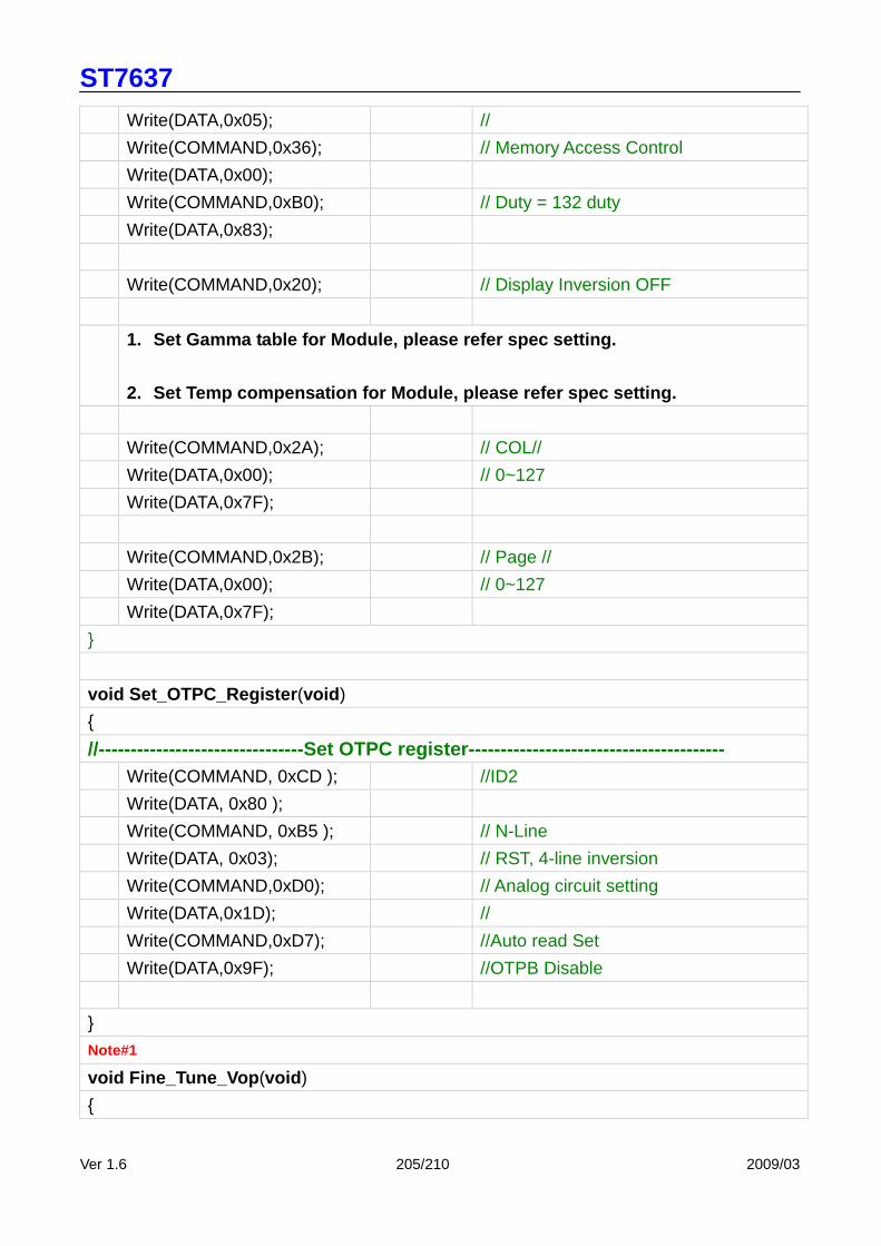
ST7637
Ver 1.6 205/210 2009/03
Write(DATA,0x05); //
Write(COMMAND,0x36); // Memory Access Control
Write(DATA,0x00);
Write(COMMAND,0xB0); // Duty = 132 duty
Write(DATA,0x83);
Write(COMMAND,0x20); // Display Inversion OFF
1. Set Gamma table for Module, please refer spec se tting.
2. Set Temp compensation for Module, please refer s pec setting.
Write(COMMAND,0x2A); // COL//
Write(DATA,0x00); // 0~127
Write(DATA,0x7F);
Write(COMMAND,0x2B); // Page //
Write(DATA,0x00); // 0~127
Write(DATA,0x7F);
void Set_OTPC_Register (void )
//--------------------------------Set OTPC register ---------------------------------------- Write(COMMAND, 0xCD ); //ID2
Write(DATA, 0x80 );
Write(COMMAND, 0xB5 ); // N-Line
Write(DATA, 0x03); // RST, 4-line inversion
Write(COMMAND,0xD0); // Analog circuit setting
Write(DATA,0x1D); //
Write(COMMAND,0xD7); //Auto read Set
Write(DATA,0x9F); //OTPB Disable
Note#1
void Fine_Tune_Vop (void )
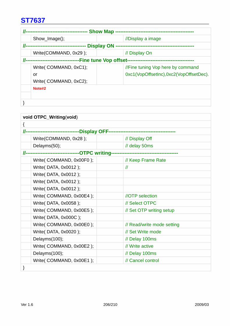
ST7637
Ver 1.6 206/210 2009/03
//------------------------------------- Show Map -- --------------------------------------------- Show_Image(); //Display a image
//------------------------------------ Display ON - ---------------------------------------------- Write(COMMAND, 0x29 ); // Display On
//--------------------------------Fine tune Vop off set----------------------------------------
Write( COMMAND, 0xC1);
or
Write( COMMAND, 0xC2);
//Fine tuning Vop here by command
0xc1(VopOffsetInc),0xc2(VopOffsetDec).
Note#2
void OTPC_Writing (void )
//--------------------------------Display OFF------ ---------------------------------- Write(COMMAND, 0x28 ); // Display Off
Delayms(50); // delay 50ms
//--------------------------------OTPC writing----- ----------------------------------- Write( COMMAND, 0x00F0 ); // Keep Frame Rate
Write( DATA, 0x0012 ); //
Write( DATA, 0x0012 );
Write( DATA, 0x0012 );
Write( DATA, 0x0012 );
Write( COMMAND, 0x00E4 ); //OTP selection
Write( DATA, 0x0058 ); // Select OTPC
Write( COMMAND, 0x00E5 ); // Set OTP writing setup
Write( DATA, 0x000C );
Write( COMMAND, 0x00E0 ); // Read/write mode setting
Write( DATA, 0x0020 ); // Set Write mode
Delayms(100); // Delay 100ms
Write( COMMAND, 0x00E2 ); // Write active
Delayms(100); // Delay 100ms
Write( COMMAND, 0x00E1 ); // Cancel control
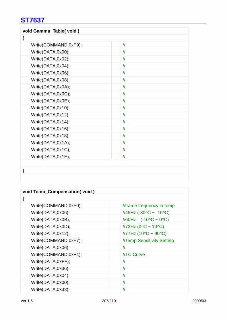
ST7637
Ver 1.6 207/210 2009/03
void Gamma_Table( void )
Write(COMMAND,0xF9); //
Write(DATA,0x00); //
Write(DATA,0x02); //
Write(DATA,0x04); //
Write(DATA,0x06); //
Write(DATA,0x08); //
Write(DATA,0x0A); //
Write(DATA,0x0C); //
Write(DATA,0x0E); //
Write(DATA,0x10); //
Write(DATA,0x12); //
Write(DATA,0x14); //
Write(DATA,0x16); //
Write(DATA,0x18); //
Write(DATA,0x1A); //
Write(DATA,0x1C); //
Write(DATA,0x1E); //
void Temp_Compensation( void )
Write(COMMAND,0xF0); //frame frequency in temp
Write(DATA,0x06); //45Hz (-30^C ~ -10^C)
Write(DATA,0x0B); //60Hz (-10^C ~ 0^C)
Write(DATA,0x0D); //72Hz (0^C ~ 10^C)
Write(DATA,0x12); //77Hz (10^C ~ 90^C)
Write(COMMAND,0xF7); //Temp Sensitivity Setting
Write(DATA,0x06); //
Write(COMMAND,0xF4); //TC Curve
Write(DATA,0xFF); //
Write(DATA,0x36); //
Write(DATA,0x04); //
Write(DATA,0x00); //
Write(DATA,0x33); //

ST7637
Ver 1.6 208/210 2009/03
Write(DATA,0x42); //
Write(DATA,0xC4); //
Write(DATA,0x59); //
Note: #1 If the Vop and display performance is not suita ble after burning OTP ,,,,the Vop has to refine tune.
#2 In this section”+” & “-“ key button, please exe cute Write(COMMAND,0xC1) to increase one step at
Vop and execute Write(COMMAND,0xC2) to decrease one step at Vop, if necessary.
#3 The TC is turn on in burning flow. If LCD modul e is too dark or bright, it’s an effect of backligh t.

ST7637
Ver 1.6 209/210 2009/03
A6- selection of application voltage Vop requirement: [Vdda x BS x BE] ≧ Vop
BS is Vop booster stage and BE is booster efficiency. Referential values are listed
below: (assume Vdda=2.8V, Vop booster stage=x8)
n-line setting=0x00: BE=77%
n-line setting=0x01: BE=66%
n-line setting=0x06: BE=74%
actual BE should be determined by adding module loading and ITO resistance value. Vdda<3V: 3V≦Vg≦2xVdda, Vdda≧3V: 1.8V≦Vg≦2xVdda.
Vm=Vg/2 and 0.7V<Vm<Vdda-0.7V.
The worst condition should be considered:
Low temperature effect and display on with gray pattern on panel.
Referential LCD module setting
Condition:Vdda=2.8V, Vop booster stage=x8, booster level=level 2, duty=1/132, panel
size=1.5”
bias Vop (n-line=0x00) Vop (n-line=0x01) Vop (n-line=0x06)
1/10 15V~17.24V 14.78V 15V~16.57V
1/9 13.5V~17.24V 13.5V~14.78V 13.5V~16.57V
Note:it is recommended to reserve some range for user adjustment and temperature effect.

ST7637
Ver 1.6 210/210 2009/03
ST7637 Serial Specification Revision History
Version Date Description
0.x Preliminary version
1.0 2007/01 First issue
1.1 2007/03
1. Modfity Application Note example circuit ST7637 pad name
2. Remove command B4h.
3. Modify resolution value of example2 in vertical scroll example.
1.2 2007/04
1. Specify OTP and OTPB register.
2. Modify application note A1b and A1d.
3. Modify application note A3 for abnormal power off.
1.3 2007/05 1. Redefine the programming mechanism of non-volatility memory.
2. Modify type error in command 0xC2h.
1.4 2007/10
1. Specify relationship between Vg, Vdda and Vddi.
2. Add application note for selection of application voltage.
3. Redefine the value of sleep current.
1.5 2008/07
1. Remove external clock function.
2. Fix type error in command 0x0F.
3. Remove ID code setting and modify temperature compensation
setting suggestion in initial code.
4. Remove un-necessary characteristics.
1.6 2009/03 1. Correct some type errors.
Related Documents