ROLL TO ROLL MANUFACTURING OF FLEXIBLE ELECTRONIC DEVICES By MUTHAPPA PONJANDA-MADAPPA Bachelor of Science in Mechanical Engineering Visveswaraiah Technological University Belgaum, Karnataka, India 2006 Submitted to the Faculty of the Graduate College of Oklahoma State University in partial fulfillment of the requirements for the Degree of MASTER OF SCIENCE December, 2011

Welcome message from author
This document is posted to help you gain knowledge. Please leave a comment to let me know what you think about it! Share it to your friends and learn new things together.
Transcript
ROLL TO ROLL MANUFACTURING OF FLEXIBLE
ELECTRONIC DEVICES
By
MUTHAPPA PONJANDA-MADAPPA
Bachelor of Science in Mechanical EngineeringVisveswaraiah Technological University
Belgaum, Karnataka, India2006
Submitted to the Faculty of theGraduate College of
Oklahoma State Universityin partial fulfillment ofthe requirements for
the Degree ofMASTER OF SCIENCE
December, 2011
ROLL TO ROLL MANUFACTURING OF FLEXIBLE
ELECTRONIC DEVICES
Thesis Approved:
Dr. Prabhakar R. Pagilla
Thesis Advisor
Dr. Gary E. Young
Committe Member
Dr. John J. Shelton
Committe Member
Dr. Sheryl A. Tucker
Dean of the Graduate College
ii
TABLE OF CONTENTS
Chapter Page
1 INTRODUCTION 1
1.0.1 Flexible Electronics . . . . . . . . . . . . . . . . . . . . . . . . 1
1.0.2 History of Flexible Electronics . . . . . . . . . . . . . . . . . . 7
1.0.3 Roll to Roll (RTR) Manufacturing . . . . . . . . . . . . . . . 9
1.0.4 Web Handling . . . . . . . . . . . . . . . . . . . . . . . . . . . 10
1.0.5 Contributions . . . . . . . . . . . . . . . . . . . . . . . . . . . 11
2 ORGANIC LIGHT EMITTING DIODES AND SOLAR CELLS 14
2.1 Organic Light Emitting Diode (OLED) . . . . . . . . . . . . . . . . . 14
2.1.1 Components of OLEDs . . . . . . . . . . . . . . . . . . . . . . 15
2.1.2 Light Emission Process of an OLED . . . . . . . . . . . . . . 16
2.1.3 Methods of Deposition of Materials for Different OLED Layers 18
2.1.4 Substrate Materials . . . . . . . . . . . . . . . . . . . . . . . . 23
2.1.5 Color Generation . . . . . . . . . . . . . . . . . . . . . . . . . 25
2.1.6 OLED Emission Types . . . . . . . . . . . . . . . . . . . . . . 27
2.1.7 OLED Type Based on Construction . . . . . . . . . . . . . . . 27
2.1.8 OLED Type Based on the Material Type . . . . . . . . . . . . 32
2.1.9 Differences Between Inorganic LEDs and OLEDs . . . . . . . 32
2.1.10 Differences Between Dry Coated and Wet Coated OLEDs . . . 33
2.1.11 Flexible OLEDs . . . . . . . . . . . . . . . . . . . . . . . . . . 33
2.1.12 Advantages and Disadvantages of OLED Devices . . . . . . . 40
2.1.13 Challenges Faced in Manufacturing of OLEDs . . . . . . . . . 42
iii
2.1.14 OLED Based Light Sources . . . . . . . . . . . . . . . . . . . 43
2.1.15 OLED Display Device . . . . . . . . . . . . . . . . . . . . . . 46
2.2 Solar Cells . . . . . . . . . . . . . . . . . . . . . . . . . . . . . . . . . 52
2.2.1 Introduction . . . . . . . . . . . . . . . . . . . . . . . . . . . . 52
2.2.2 Flexible Solar Cells . . . . . . . . . . . . . . . . . . . . . . . . 54
2.2.3 Anode Layer Fabrication . . . . . . . . . . . . . . . . . . . . . 55
2.2.4 Fabrication of active layers . . . . . . . . . . . . . . . . . . . . 57
2.2.5 Fabrication of cathode layer . . . . . . . . . . . . . . . . . . . 57
2.2.6 Lamination of the barrier layer . . . . . . . . . . . . . . . . . 58
3 Roll to Roll Manufacture of Flexible Electronic Devices 67
3.1 Solution Printed Flexible OLEDs . . . . . . . . . . . . . . . . . . . . 69
3.2 Design of a Web Line for Patterning of ITO Anode Layer on PET
Substrate . . . . . . . . . . . . . . . . . . . . . . . . . . . . . . . . . 70
3.2.1 Screen Printing of Etch Resistant Material . . . . . . . . . . . 71
3.2.2 Ultra Violet (UV) curing . . . . . . . . . . . . . . . . . . . . . 78
3.2.3 Etching . . . . . . . . . . . . . . . . . . . . . . . . . . . . . . 83
3.2.4 Stripping . . . . . . . . . . . . . . . . . . . . . . . . . . . . . 84
3.3 Design of a Web Line for Deposition of Active and Cathode Layers . 86
3.3.1 Gravure Printing . . . . . . . . . . . . . . . . . . . . . . . . . 86
3.3.2 Drying Methods . . . . . . . . . . . . . . . . . . . . . . . . . . 88
3.3.3 Web Handling . . . . . . . . . . . . . . . . . . . . . . . . . . . 88
3.3.4 Determination of Web Tension and Speed in the Two Web Lines 92
3.3.5 Encapsulation of Barrier Layer . . . . . . . . . . . . . . . . . 94
3.3.6 Registration . . . . . . . . . . . . . . . . . . . . . . . . . . . . 97
4 Modeling and Simulation of Web Lines Designed for Manufacture
of Flexible Electronic Devices 108
iv
4.1 Introduction . . . . . . . . . . . . . . . . . . . . . . . . . . . . . . . . 108
4.1.1 Calculation of Drag Force on theWeb During Transport Through
a Liquid Bath . . . . . . . . . . . . . . . . . . . . . . . . . . . 108
4.1.2 Drag Force Calculation . . . . . . . . . . . . . . . . . . . . . . 110
4.2 Modeling and Simulation of the Web Line for Patterning of the Anode
Layer on PET Substrate . . . . . . . . . . . . . . . . . . . . . . . . . 114
4.3 Tension Models for Lamination of Webs . . . . . . . . . . . . . . . . 120
4.4 Web Line for Barrier Lamination to the Substrate for Flexible Electronics125
4.4.1 Pressure Sensitive Adhesive (PSA) tape . . . . . . . . . . . . 127
4.4.2 Barrier Material . . . . . . . . . . . . . . . . . . . . . . . . . . 129
4.4.3 Lamination of Barrier Material to Adhesive Layer . . . . . . . 129
4.5 Calculation of Reference Tension . . . . . . . . . . . . . . . . . . . . 133
5 Summary and Future Work 141
5.1 Summary . . . . . . . . . . . . . . . . . . . . . . . . . . . . . . . . . 141
5.2 Future Work . . . . . . . . . . . . . . . . . . . . . . . . . . . . . . . . 143
BIBLIOGRAPHY 145
v
LIST OF TABLES
Table Page
2.1 Minimum Requirement for Polymeric Materials to be used for FOLEDs 35
2.2 Important Properties of Some Polymeric Materials . . . . . . . . . . . 36
2.3 Typical values for OLED layer thickness . . . . . . . . . . . . . . . . 53
2.4 Requirements and function of each layers of a solar cell . . . . . . . . 65
2.5 Requirements and function of each layers of a solar cell . . . . . . . . 66
3.1 Typical values for printing parameters . . . . . . . . . . . . . . . . . 105
3.2 Comparison of mainstream lamination and coating processes . . . . . 106
3.3 Comparison between wet and dry adhesive lamination . . . . . . . . 107
4.1 Composition of Cupric Chloride Solution . . . . . . . . . . . . . . . . 113
4.2 Simulation Parameters . . . . . . . . . . . . . . . . . . . . . . . . . . 136
4.3 Layers of Polymer Solar Cell and their Properties . . . . . . . . . . . 137
vi
LIST OF FIGURES
Figure Page
1.1 Flexible Electronic Display [1] . . . . . . . . . . . . . . . . . . . . . . 3
1.2 A4-sized Color Electronic-Paper [2] . . . . . . . . . . . . . . . . . . . 3
1.3 Samsung OLED TV [3] . . . . . . . . . . . . . . . . . . . . . . . . . . 4
1.4 Flexible Solar Cell Panel [4] . . . . . . . . . . . . . . . . . . . . . . . 4
1.5 Flexible Electronics [5] . . . . . . . . . . . . . . . . . . . . . . . . . . 5
1.6 Advancement in the Field of Display Electronics [6] . . . . . . . . . . 6
1.7 Artificial Muscles [7] . . . . . . . . . . . . . . . . . . . . . . . . . . . 6
1.8 Simple Schematic Diagram of RTR Manufacturing Process . . . . . . 10
2.1 Parts of an OLED [18] . . . . . . . . . . . . . . . . . . . . . . . . . . 15
2.2 Light Emission Process of OLED [19] . . . . . . . . . . . . . . . . . . 17
2.3 Vacuum Deposition Method [20] . . . . . . . . . . . . . . . . . . . . . 18
2.4 Laser Ablation [21] . . . . . . . . . . . . . . . . . . . . . . . . . . . . 22
2.5 Ink-jet Deposition Method [20] . . . . . . . . . . . . . . . . . . . . . 23
2.6 Color Generation [20] . . . . . . . . . . . . . . . . . . . . . . . . . . . 26
2.7 Bottom Emitting OLED [20] . . . . . . . . . . . . . . . . . . . . . . . 28
2.8 Top Emitting OLED [20] . . . . . . . . . . . . . . . . . . . . . . . . . 28
2.9 Passive Matrix OLED (PMOLED) [22] . . . . . . . . . . . . . . . . . 29
2.10 Active Matrix OLED (AMOLED) [22] . . . . . . . . . . . . . . . . . 30
2.11 Basix Pixel Addressing Circuit for AMOLED [20] . . . . . . . . . . . 31
2.12 WVTR and OTR requirement for Electronic Devices [23] . . . . . . . 39
2.13 OLED Light Source [24] . . . . . . . . . . . . . . . . . . . . . . . . . 44
vii
2.14 OLED Layers for the Light Source [24] . . . . . . . . . . . . . . . . . 47
2.15 OLED Display Device [25] . . . . . . . . . . . . . . . . . . . . . . . . 47
2.16 Exploded View of the Display Device [26] . . . . . . . . . . . . . . . . 49
2.17 Schematic Diagram of Circuit in the Display Area [26] . . . . . . . . 51
2.18 ITO Patterning for the Solar Cell Anode Layer [17] . . . . . . . . . . 56
2.19 Silver Print on top of ITO Pattern for Three Different Module Lengths
[17] . . . . . . . . . . . . . . . . . . . . . . . . . . . . . . . . . . . . . 56
2.20 Solar Cell Structure [29] . . . . . . . . . . . . . . . . . . . . . . . . . 59
2.21 Front View, Side View and Back View of a Solar Lamp [30] . . . . . . 60
2.22 Solar Cell Lighted Lamp [30] . . . . . . . . . . . . . . . . . . . . . . . 61
2.23 Exploded view of the solar lamp assembly [30] . . . . . . . . . . . . 63
3.1 Flat Bed Screen Printing . . . . . . . . . . . . . . . . . . . . . . . . . 100
3.2 Rotary Screen Printing [43] . . . . . . . . . . . . . . . . . . . . . . . 100
3.3 Rotary Screen Printing [32] . . . . . . . . . . . . . . . . . . . . . . . 101
3.4 Support Tube for Rotary Screen Printing [44] . . . . . . . . . . . . . 101
3.5 Web Line for Patterning ITO . . . . . . . . . . . . . . . . . . . . . . 101
3.6 Web Line for Deposition of Active Layers and Cathode . . . . . . . . 102
3.7 Gravure Printing [45] . . . . . . . . . . . . . . . . . . . . . . . . . . . 102
3.8 Displacement Guide [46] . . . . . . . . . . . . . . . . . . . . . . . . . 102
3.9 Vacuum Rollers [47] . . . . . . . . . . . . . . . . . . . . . . . . . . . . 103
3.10 Accumulator [48] . . . . . . . . . . . . . . . . . . . . . . . . . . . . . 103
3.11 Cooling Roller [36] . . . . . . . . . . . . . . . . . . . . . . . . . . . . 104
3.12 Schematic of Two Successive Print Units with Compensator Roller [42] 104
4.1 Liquid Bath . . . . . . . . . . . . . . . . . . . . . . . . . . . . . . . . 109
4.2 Control Scheme for Regulating Web Tension and Web Velocity . . . . 115
4.3 Simplified Web Line for Modeling and Simulation . . . . . . . . . . . 116
viii
4.4 Cross-sectional View of Unwind Roll . . . . . . . . . . . . . . . . . . 117
4.5 Free-body Diagram of Master Speed Roller . . . . . . . . . . . . . . . 118
4.6 Lamination of Two Webs . . . . . . . . . . . . . . . . . . . . . . . . . 122
4.7 Lamination of Two Webs . . . . . . . . . . . . . . . . . . . . . . . . . 123
4.8 Pressure Sensitive Adhesive Tape [59] . . . . . . . . . . . . . . . . . . 127
4.9 Web Line for Lamination of Barrier Layer to the Adhesive Material . 130
4.10 Web Line for Lamination of Barrier Layer to the Solar Cell Substrate 131
4.11 Simplified Line for Modeling and Simulation of Lamination Web Line 132
4.12 Simulations for the Web Line for Patterning ITO . . . . . . . . . . . 135
4.13 Simulations for the Web Line for Patterning ITO . . . . . . . . . . . 137
4.14 Simulations for the Web Line for Patterning ITO . . . . . . . . . . . 138
4.15 Simulations for the Web Line for Patterning ITO . . . . . . . . . . . 139
4.16 Simulations for the Lamination Web Line . . . . . . . . . . . . . . . . 140
ix
NOMENCLATURE
A Area of cross-section of web
Bfe, Bfp Coefficient of viscous friction
b Viscous damping coefficient
bf Coefficient of friction
c Specific heat of the web
E Young’s modulus of web material
f Blasius similarity function
Fc Disturbing force on the carriage
Fd Drag Force
g Acceleration due to gravity
h Thickness of web
J Moment of Inertia of the roller
k Dimensionless empirical constant
L Length of the web in a bath
Li Length of the ith span
mf Mass fraction
M Mass fraction
Mc Mass of the carriage
m Mass of the web
N Number of spans in the accumulator
n Speed ratio
p Empirical constant
x
R Radius of the roller
Ri Radius of rollers/pulley
Rco Outer radius of the core-shaft with core on it
s Blasius similarity function for crosswise flow
T Temperature
t Time
tc Average Tension in the accumulator
ti Web tension in the ith span
Uw Velocity of the web in the x-direction
U∞ Velocity of the fluid in the x-direction
U0 Reference velocity in the x-direction
u Control torque
ue, up Control inputs on the entry/process side rollers
V volume
v Average web velocity
v Web velocity
X Mixture
xc Displacement of accumulator carriage
vc Velocity of accumulator carriage
vi Velocity of web on ith roller/roll
W0 Initial velocity of the fluid in the crosswise direction
w Width of the web
W Width of the specimen
x Position in the x-direction
ρ Density of the web material
ψ Stream function
η Similarity Variable
xi
Density of the fluid
ν Kinematic viscosity of the fluid
τ Shear stress
λ velocity ratio
ǫ Strain
σ Stress
Subscripts
A,B Layers of webs
c pertaining to the composite web
i span or roller number
m mixture
R pertaining to the roller
s stretched state
w pertaining to the web
W pertaining to the water
Acronyms
OLED Organic Light Emitting Diode
PET Poly Ethylene Terephthalate
AMOLED Active Matrix Organic Light Emitting Diode
PMOLED Passive Matrix Organic Light Emitting Diode
HIL Hole Injection Layer
ETL Electron Tranport Layer
ITO Indium Tin Oxide
RTR Roll To Roll
PFBT Poly-dihexylfluorene-alt-benzothiadiazole
RFID Radio Frequency Identification Technology
xii
LCD Liquid Crystal Display
FOLED Flexible Organic Light Emitting Diode
TFT Thin Film Transistor
PECVD Plasma-Enhanced Chemical Vapor Deposition
UV Ultra Violet
pps pulses per second
OVPD Organic Vapor Phase Deposition
CCM Color Changing Media
PEN Poly Ethylene Naphthalate
PC Poly Carbonate
COC Cyclic Olefin Copolymer
PI/OMMT Polyamide/Organoclay nanocomposite
PES Poly Ether Sulphone
PDMS Poly Di Menthyl Siloxane
PVDF Poly Vinylidene Di Fluoride
PEEK Poly Ether Ether Ketone
IZO Indium Zinc Oxide
PEDOT:PSS Poly(3,4-ethylenedioxythiophene) Poly(styrenesulfonate)
OTR Oxygen Transmission Rate
WVTR Water Vapor Transmission Rate
RGB Red Green Blue
TCP Tape Carrier Package
PCB Printed Circuit Board
ESA Electro Static Assist
PSA Pressure Sensitive Adhesive
PLI pounds per linear inch
xiii
CHAPTER 1
INTRODUCTION
Electronic devices have become an integral part of human life. There are a number
of electronic devices that serve different purposes, and many of them improve the
quality of life. In some cases, the use of electronic devices has become a requirement
than a choice because of their widespread use and part of every day life. This thesis
is focused on efficient manufacture of electronic devices in flexible form using roll to
roll (RTR) method of continuous manufacturing which is expected to significantly
improve productivity and efficiency and reduce manufacturing costs.
1.0.1 Flexible Electronics
Flexible electronics is a technology where the electronic circuits are assembled on flex-
ible substrates for use. These flexible electronics are very thin, light weight, portable,
and flexible and have many advantages over rigid electronic devices. Currently, re-
searchers around the globe are trying to build flexible electronic devices in various
fields of electronics. The area of flexible electronics includes a wide range of ap-
plications such as flexible displays, flexible lighting devices, electrophoretic displays,
packaging, textiles, medical devices, flexible sensors, to name a few. The most com-
mon feature among these devices is that they can be manufactured in RTR form on
flexible substrates such as plastics, stainless steel, thin glass films without losing any
functionality. The main reasons behind the possibility of flexible electronics are the
development of solution printing techniques that are cost effective and compatible
with RTR form of manufacturing and use of polymer materials for substrates along
1
with plastic inks that can be solution printed and coated.
Many researchers, laboratories and companies are trying to develop methods to
manufacture these flexible electronic devices in RTR form. Many have already suc-
ceeded in developing devices to facilitate manufacture of many parts of flexible elec-
tronics in RTR form for some applications. There has been considerable research in
this area with respect to the materials that need to be used, manufacturing methods,
various processes involved, costs of production, etc. Currently, even though some
researchers and companies have succeeded in such manufacturing, the costs involved
in the production are quite high compared to batch process method. It is impor-
tant to optimize the manufacturing of flexible devices with regard to the materials,
production methods, etc. These flexible electronics may be flexed, bent and rolled
to an extent and would still be expected to function without losing their durability.
Flexible electronic devices have already come to the market. For example, Figure
1.1 shows a flexible electronic display prototype developed by HP and the Flexible
Display Center at Arizona State University.
Flexible electronic paper promises to replace newspapers in the future. For ex-
ample, Figure 1.2 shows a thin and flexible electronic paper that has been developed
by LG Philips. This type of flexible electronic paper uses wireless communications to
update the information and make the news readily available to the consumers.
Flexible OLED television devices have already come to the market. OLED display
technology promises to replace the Liquid Crystal Display (LCD) display technology
in the near future. Figure 1.3 shows a 14 inch OLED prototype television invented
by Samsung company.
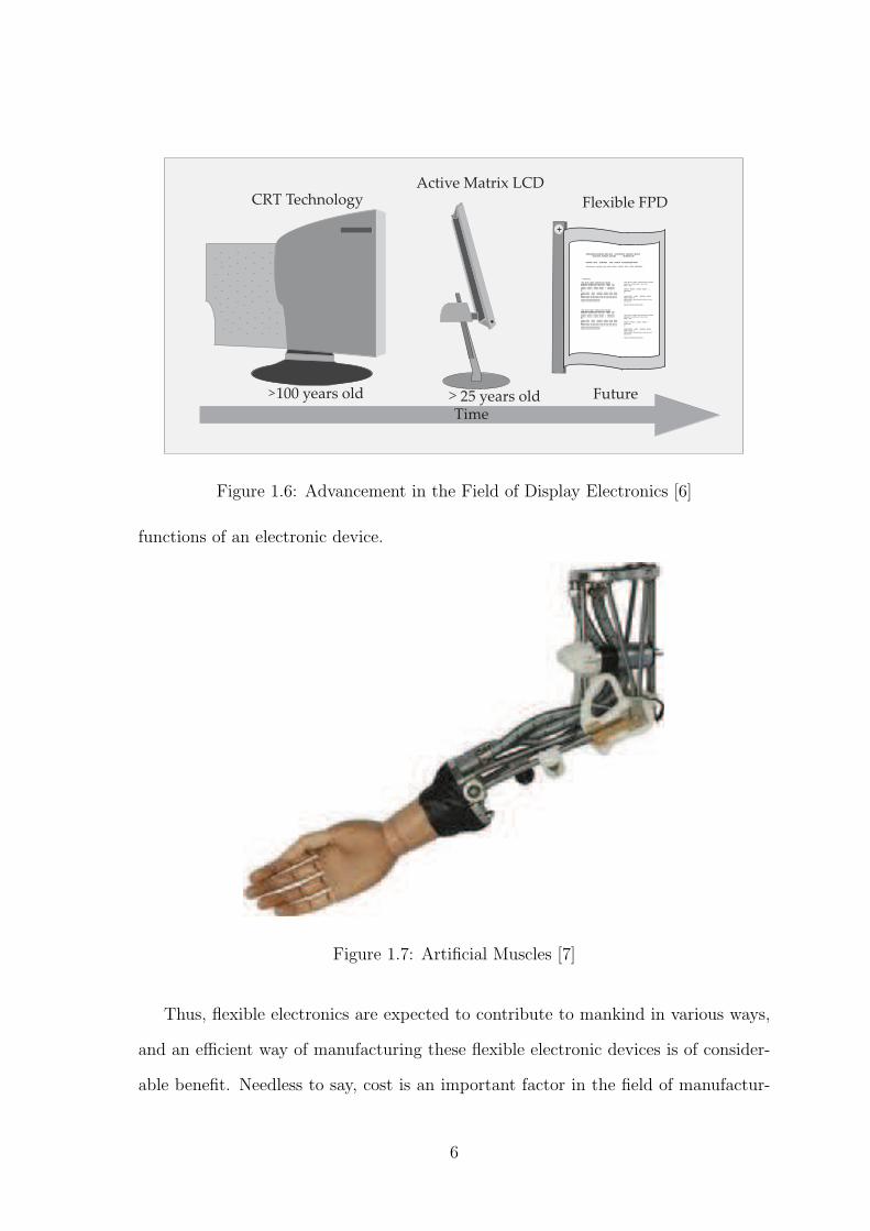
Polymer based solar cells are promising alternatives for conventional energy sources.
They are energy efficient, flexible, and more easily processed than rigid solar cells.
Flexible solar panels are already in the market. Figure 1.4 shows a flexible solar cell
panel that is manufactured by silicon solar solutions and is available to the consumers.
2
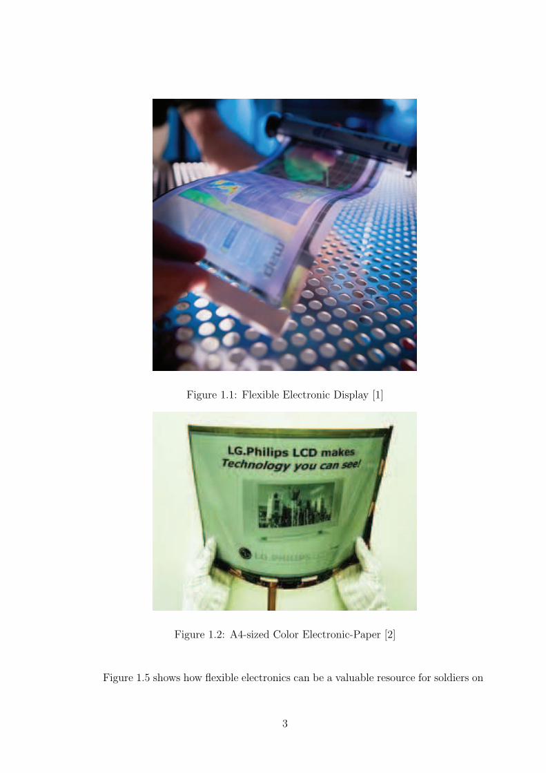
Figure 1.1: Flexible Electronic Display [1]
Figure 1.2: A4-sized Color Electronic-Paper [2]
Figure 1.5 shows how flexible electronics can be a valuable resource for soldiers on
3
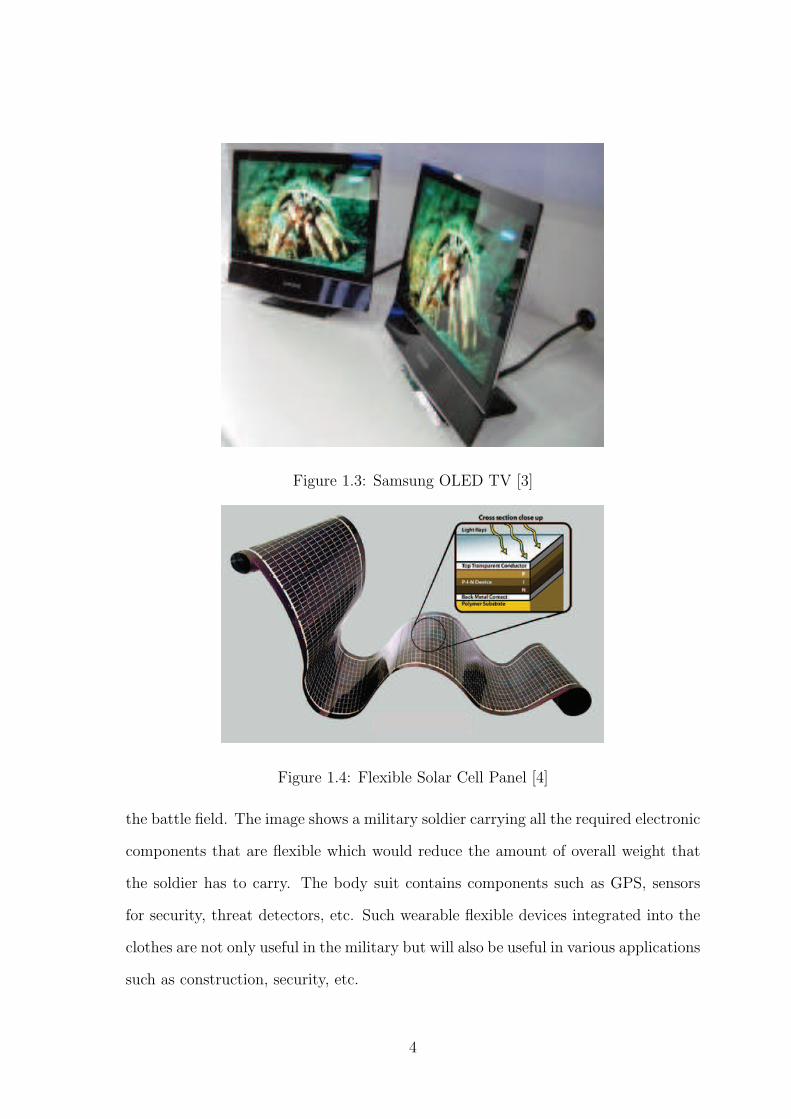
Figure 1.3: Samsung OLED TV [3]
Figure 1.4: Flexible Solar Cell Panel [4]
the battle field. The image shows a military soldier carrying all the required electronic
components that are flexible which would reduce the amount of overall weight that
the soldier has to carry. The body suit contains components such as GPS, sensors
for security, threat detectors, etc. Such wearable flexible devices integrated into the
clothes are not only useful in the military but will also be useful in various applications
such as construction, security, etc.
4
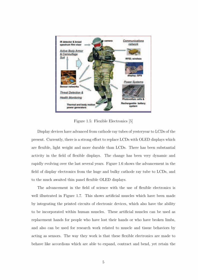
Figure 1.5: Flexible Electronics [5]
Display devices have advanced from cathode ray tubes of yesteryear to LCDs of the
present. Currently, there is a strong effort to replace LCDs with OLED displays which
are flexible, light weight and more durable than LCDs. There has been substantial
activity in the field of flexible displays. The change has been very dynamic and
rapidly evolving over the last several years. Figure 1.6 shows the advancement in the
field of display electronics from the huge and bulky cathode ray tube to LCDs, and
to the much awaited thin panel flexible OLED displays.
The advancement in the field of science with the use of flexible electronics is
well illustrated in Figure 1.7. This shows artificial muscles which have been made
by integrating the printed circuits of electronic devices, which also have the ability
to be incorporated within human muscles. These artificial muscles can be used as
replacement hands for people who have lost their hands or who have broken limbs,
and also can be used for research work related to muscle and tissue behaviors by
acting as sensors. The way they work is that these flexible electronics are made to
behave like accordions which are able to expand, contract and bend, yet retain the
5
sddfdsfdfdsfsd sdfsdfsdgf sdfdsf sdfsdf sdfsdfsdfsdfsdf sdfsdfsdfsd sdfsdfsdf
dasfdsfsdfds dfsdfsdfsd sdfsdfsdfd fdfsdfdfsdfsd fdf
dssdfsdf sdfsdf dfsdfsdfdfd dfsdf sdfsdfsdf dsfsdfsdfsdfsdfdf dfdfd
sdfdfsdf dgdfg sdgsdfgdg gfgfg dfgfhf dfhdfhh dfhdfhfh fhfhfh fhfhhh fhfhhfhfhhhh
sdfdf sdfsdfd sdfdfdf sdfdfdfsdfsdfsdf dfdfdfdf
dfdfdfdfdf sdfsdfdf sdfsdf sdfsdf dfdf fdfdfd dfdf
dfdfdfdf dfdfdfd d fdfdfdf dfdfdfd n ddfdfddfd
df
ddfdfdf dfdfdf dfdfdf dfdfdfdfd dfdfdfd dfdfdf dfdfdf
df
dfdfdfd dfdfdf sdfsdfdf dfdfds dsfdf dfd dfdf dfdf dfd fdf
fdfdfdf dfdfd fdfd fdfd fdfd fdfd.
sdfdf sdfsdfd sdfdfdf sdfdfdfsdfsdfsdf dfdfdfdf
dfdfdfdfdf sdfsdfdf sdfsdf sdfsdf dfdf fdfdfd dfdf
dfdfdfdf dfdfdfd d fdfdfdf dfdfdfd n ddfdfddfd
df
ddfdfdf dfdfdf dfdfdf dfdfdfdfd dfdfdfd dfdfdf dfdfdf
df
dfdfdfd dfdfdf sdfsdfdf dfdfds dsfdf dfd dfdf dfdf dfd fdf
fdfdfdf dfdfd fdfd fdfd fdfd fdfd.
sdfdf sdfsdfd sdfdfdf sdfdfdfsdfsdfsdf dfdfdfdf
dfdfdfdfdf sdfsdfdf sdfsdf sdfsdf dfdf
fdfdfd dfdf
dfdfdfdf dfdfdfd d fdfdfdf dfdfdfd n
ddfdfddfd
df
ddfdfdf dfdfdf dfdfdf dfdfdfdfd dfdfdfd
dfdfdf dfdfdf df
dfdfdfd dfdfdf sdfsdfdf dfdfds dsfdf dfd dfdf
dfdf dfd fdf
fdfdfdf dfdfd fdfd fdfd fdfd fdfd.
sdfdf sdfsdfd sdfdfdf sdfdfdfsdfsdfsdf dfdfdfdf
dfdfdfdfdf sdfsdfdf sdfsdf sdfsdf dfdf
fdfdfd dfdf
dfdfdfdf dfdfdfd d fdfdfdf dfdfdfd n
ddfdfddfd
df
ddfdfdf dfdfdf dfdfdf dfdfdfdfd dfdfdfd
dfdfdf dfdfdf df
dfdfdfd dfdfdf sdfsdfdf dfdfds dsfdf dfd dfdf
dfdf dfd fdf
fdfdfdf dfdfd fdfd fdfd fdfd fdfd.
sdfdf sdfsdfd sdfdfdf sdfdfdfsdfsdfsdf dfdfdfdf
dfdfdfdfdf sdfsdfdf sdfsdf sdfsdf dfdf fdfdfd dfdf
dfdfdfdf dfdfdfd d fdfdfdf dfdfdfd n ddfdfddfd
df
ddfdfdf dfdfdf dfdfdf dfdfdfdfd dfdfdfd dfdfdf dfdfdf
df
dfdfdfd dfdfdf sdfsdfdf dfdfds dsfdf dfd dfdf dfdf dfd fdf
fdfdfdf dfdfd fdfd fdfd fdfd fdfd.
sdfdf sdfsdfd sdfdfdf sdfdfdfsdfsdfsdf dfdfdfdf
dfdfdfdfdf sdfsdfdf sdfsdf sdfsdf dfdf fdfdfd dfdf
dfdfdfdf dfdfdfd d fdfdfdf dfdfdfd n ddfdfddfd
df
ddfdfdf dfdfdf dfdfdf dfdfdfdfd dfdfdfd dfdfdf dfdfdf
df
dfdfdfd dfdfdf sdfsdfdf dfdfds dsfdf dfd dfdf dfdf dfd fdf
fdfdfdf dfdfd fdfd fdfd fdfd fdfd.
Introduction
100 years old 25 years old Future
CRT TechnologyActive Matrix LCD
Flexible FPD
Time
Figure 1.6: Advancement in the Field of Display Electronics [6]
functions of an electronic device.
Figure 1.7: Artificial Muscles [7]
Thus, flexible electronics are expected to contribute to mankind in various ways,
and an efficient way of manufacturing these flexible electronic devices is of consider-
able benefit. Needless to say, cost is an important factor in the field of manufactur-
6
ing. The method developed for the manufacture of these electronic devices should
be efficient, economical and cost effective. If these devices are manufactured in a
continuous process, it will be beneficial with respect to every regard. Manufacture
of flexible electronics using RTR methods over batch process methods is expected to
help in reducing the total capital costs of the equipment, display device cost, and
substantially increase the throughput of manufacturing. One of the main challenges
faced in the development of flexible electronics is in the complete sealing of the de-
vices as these devices have to be protected from entering of environmental permeates
such as oxygen and moisture. This is very critical for the long term working of the
devices.
Flexible devices such as OLEDs, RFID, polymer solar cells have very thin structure
including the active layers deposited on the substrate. The total thickness of the active
layers is less than a micron and each of the layers are flexible, which has given rise to
a new revolution in the electronics market.
1.0.2 History of Flexible Electronics
The first flexible solar cell array was manufactured in the year 1960 by slimming single
crystal silicon wafer cells and combining them together with plastic substrate such
that they become flexible. Due to the energy crisis that took place in the year 1973,
there was lot of encouragement towards the development of thin film flexible solar cells
in order to reduce the cost of producing electricity using photovoltaic materials. In
the year 1976, a Schottky barrier solar cell was developed on a stainless steel substrate
by Wronski, Carlson and Daniel at RCA laboratories. Plattner et al. and Okaniwa
et al. developed solar cells on plastic substrates in the early 1980s. In the year 1985,
P. Nath and M. Izu reported the fabrication of flexible solar cells by RTR method.
They used glow discharge deposition method to deposit the layers on to stainless
steel substrate [8]. In the year 1986, RTR fabrication of solar cells on polymeric
7
substrates were introduced by Okaniwa and his coworkers at their Central Research
laboratories in Tokyo [9]. They used continuous glow discharge methods in RTR form
in order to deposit the silicon layers on a flexible polymer substrate. The first Thin
Film Transistors (TFTs) were made by Brody and his colleagues in the year 1968.
They manufactured TFT made of tellurium on paper strip and also proposed the
idea of using TFT matrices to address display devices. They also made several TFTs
on different substrates such as Mylar, polyethylene, anodized aluminum foil in the
succeeding years. Constant et al. demonstrated TFT circuits on flexible polyamide
substrates at Iowa State University in the year 1994. In the year 1997, silicon TFTs
made on plastic substrates using laser annealing methods were reported. In the year
1996, Smith and his coworkers reported the deposition of thin film silicon films on
polyester substrates using excimer laser crystallization and doping methods [10]. In
the year 1997, N. D. Young and his coworkers reported the fabrication of poly-silicon
TFTs’s on polyamide substrates and polyethersulphane substrates [11]. They used
excimer laser crystallization technique and PECVD methods for deposition of silicon
materials. Over the years, research in the field of flexible electronics has expanded
vastly and many researchers have demonstrated the manufacture of flexible devices
on various substrates such as plastic, thin glass substrates, stainless steel, etc. For
example, in the year 2006, researchers have fabricated a FOLED in a vacuum-free
lamination process by laminating an anode component and cathode component of an
OLED using a roll laminator [12]. In the year 2005, researchers have demonstrated
a flexible OLED using cyclic olefin copolymer (COC) as the substrate [13]. In the
year 2008, researchers have fabricated FOLED using an UV-curable epoxy resin as
an adhesive between the substrate and the anode [14]. In [15], the authors have
demonstrated a FOLED in which polymer layers were deposited by a polymer inking
and stamping method that can be employed in a RTR form of manufacturing. In
the year 2009, researchers have shown a FOLED using flexible substrate made of
8
polyamide/organoclay nanocomposite [16]. To date, flexible electronic devices such
as OLED, polymer cells, LCDs, etc., are manufactured either in a batch method or
non-continuous RTR method. These methods are expensive and inefficient. There
has been substantial breakthroughs in the field of flexible solar cells too. In the
paper [17], researchers have shown that solar cells can be manufactured in a non-
continuous RTR form. However, there has been reported activity to date which
discusses the web handling aspects of RTR manufacturing of these composite webs.
In this thesis, strategies to design web lines and web handling strategies are applied
for the manufacture of flexible electronic devices in continuous, composite web form.
1.0.3 Roll to Roll (RTR) Manufacturing
RTR manufacturing involves manufacture of flexible devices in the sheet form. The
main criteria is that the substrate material chosen should be flexible. The selection of
the material for the substrate is an important factor. The material for the substrate
should be selected such that it should be able to be bent, flexed and rolled any number
of times without losing its functionality. The suitability of many polymers/plastics
are being researched for the substrate material in order to improve the production
of flexible devices. The manufacture of electronic devices in RTR form has various
advantageous over batch processing methods. It saves time, cost, reduces delay time
and increases efficiency, throughput, performance, etc. Figure 1.8 shows a schematic
of a typical RTR system for the manufacture of a flexible device.
Currently, most of the printing methods are compatible with RTR manufacturing.
For example, there are solution printing methods such as gravure printing, screen
printing that are used to print inks on a flexible material in a RTR process. These
methods can be used to print a very thin layer of materials on the substrate and are
very efficient. Web handling involves improving the storage and transport of web
material as the web is transported on rollers through various process sections such as
9
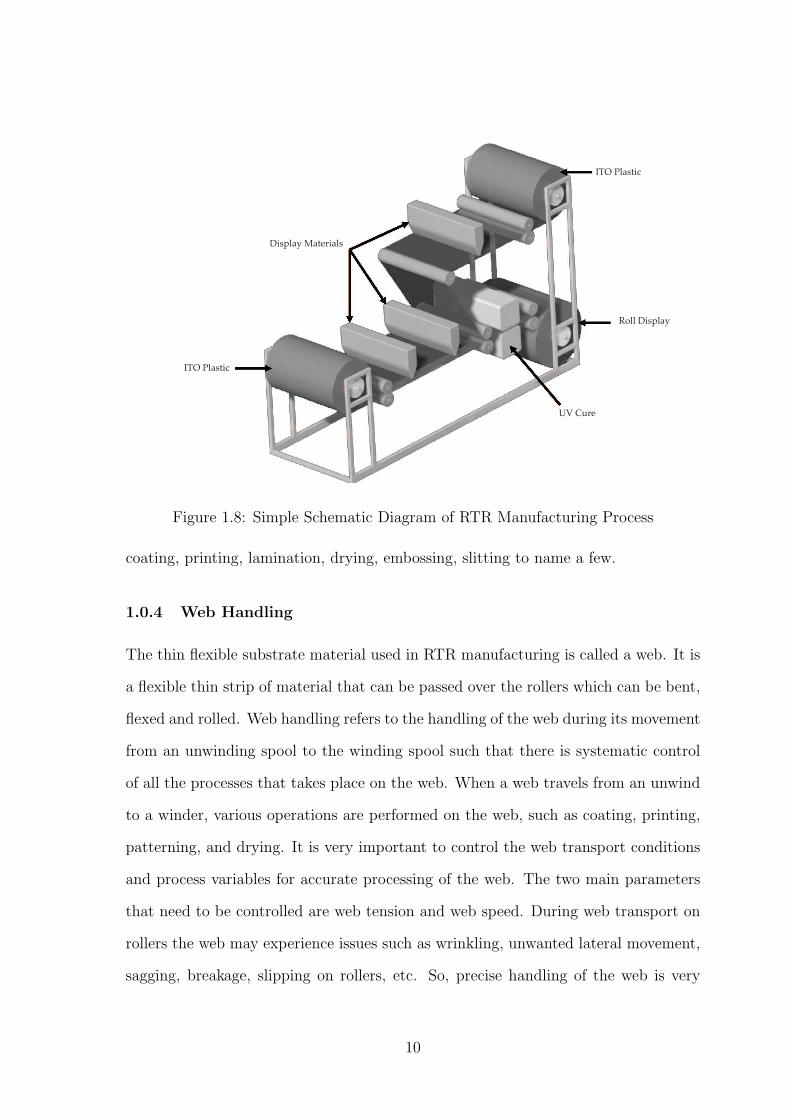
Display Materials
ITO Plastic
UV Cure
Roll Display
ITO Plastic
Figure 1.8: Simple Schematic Diagram of RTR Manufacturing Process
coating, printing, lamination, drying, embossing, slitting to name a few.
1.0.4 Web Handling
The thin flexible substrate material used in RTR manufacturing is called a web. It is
a flexible thin strip of material that can be passed over the rollers which can be bent,
flexed and rolled. Web handling refers to the handling of the web during its movement
from an unwinding spool to the winding spool such that there is systematic control
of all the processes that takes place on the web. When a web travels from an unwind
to a winder, various operations are performed on the web, such as coating, printing,
patterning, and drying. It is very important to control the web transport conditions
and process variables for accurate processing of the web. The two main parameters
that need to be controlled are web tension and web speed. During web transport on
rollers the web may experience issues such as wrinkling, unwanted lateral movement,
sagging, breakage, slipping on rollers, etc. So, precise handling of the web is very
10
important for the development of a functioning final product. In order to control
the movement of the web through a RTR process, it is very important to know the
dynamics of the rollers, properties of the web material, operating conditions of the
different processes, etc. In a high speed web handling system, as the web goes through
dynamic transitions, it might be subjected to stress and strain. The stress developed
may exceed the strength of the web material, which would result in web breakage.
This would result in an increase in downtime, wastage of material, and would reduce
the overall performance of the machine. The quality of the final product is greatly
influenced by tension and speed of the web in the web line. The main aim of the
web handling process is to transport the web with highest speed and with minimal
damage so that overall throughput of the equipment is high.
Web handling machines consist of various tools designed to transport the web
through the various processes and machines. Most of these tools are mechanics based
but even control theory plays a major role in the web handling system. The mechanics
of web handling describes the behavior of a web during its movement between two
rollers. The rollers on which the web is moving plays a vital role in maintaining the
quality of web that is being processed. Along with the material properties, the roller
structure and web’s interaction with the rollers should be carefully assessed in order
to obtain acceptable productivity. When the web travels over a roller, the roller exerts
stress on the web at the point of contact due to the traction between the roller and
web. Thus the dimension of roller, its shape and wrap angle of the web on the roller
play an important role in the precise movement of the web.
1.0.5 Contributions
The contributions of this thesis is summarized in the following:
• A comprehensive study of the literature was undertaken to understand the vari-
ous processes involved in manufacture of flexible electronics such as OLEDs and
11
solar cells, and an investigative study was carried out to highlight those pro-
cesses and methods that are suitable for RTR manufacture of flexible electronic
devices.
• Design of web lines for RTR manufacturing of flexible electronic devices was
investigated. Three web lines were designed for the manufacture of OLED
based flexible electronic devices and polymer solar cells. The first web line was
designed for the patterning of the anode layer on a plastic substrate; this web
line can be used for manufacture of many types of flexible devices. The second
web line was designed for the deposition of active layers of an OLED device on
the composite web obtained from the first line consisting of the substrate and
the patterned anode layer. The third web line was designed for the lamination
of barrier substrate to the polymer solar cell device.
• Solution printing technologies and various web handling techniques were deter-
mined such that ITO patterning was done in a continuous process. Various
processes and web line parameters were determined for the web line for RTR
patterning of ITO material.
• Process parameters and technologies were determined for the web line designed
for the deposition of the active layers of flexible OLED device on the ITO
patterned anode layer with substrate. The web line parameters and solution
printing technologies that assist in RTR manufacturing were determined for the
deposition of active layers.
• The application of various aspects of web handling such as registration, guiding,
accumulators, etc., were studied and implemented for each of the three web lines.
• A web line was designed for simultaneous lamination of barrier material to both
sides of the flexible composite web for OLEDs and polymer solar cell films. The
12
barrier material that protects the devices against oxygen and moisture was
identified from a study. Also, web line parameters for the lamination of barrier
material to the polymer solar cell device were established.
• A model for web tension for lamination of two webs was investigated. This
model was used for studying the tension behavior during simultaneous lamina-
tion of barrier materials to both sides of the solar cell substrate.
• Models for tension and velocity were used to develop a model for various spans
and rollers of the web line designed for patterning of ITO anode material. Sim-
ulations were performed for the entire web line to regulate web velocity and
tension in various spans and rollers of the line. Simulations were also conducted
for the web line used for lamination of the barrier material.
• The effect of drag force on the web as it passes through liquid bath was investi-
gated. The drag force was calculated based on the crosswise laminar movement
of the fluid in the liquid bath through which the web is transported.
13
CHAPTER 2
ORGANIC LIGHT EMITTING DIODES AND SOLAR CELLS
In this chapter an extensive study was conducted to identify and understand the
various technologies and methods available for manufacture of flexible electronics,
especially for OLED devices and polymer solar cells. The first section of the chapter
focuses on understanding the working of an OLED and its components; the materials
used for its different layers; deposition methods of its components and challenges
involved in its manufacturing. The second section discusses the operation of polymer
solar cells, its components and the function of its components.
This study was critical in understanding the processes involved in OLED and
solar cell manufacturing for the proper selection of materials that will enable the
manufacture of flexible electronic devices in RTR form. It will help in understanding
the function and properties of the materials which will aid in designing the web line
to manufacture these flexible electronics in RTR form. This chapter also provides
an insight into the construction of flexible electronics and its connection with the
electronic circuits in order to form the flexible devices such as OLED lighting, OLED
display devices, etc.
2.1 Organic Light Emitting Diode (OLED)
OLEDs emit light by the process of electroluminescence which is an optical phe-
nomenon where certain materials emit light when electric current is passed through
them. OLEDs consist of organic materials as the semiconducting materials which
produce light when electric current is passed through them. These can provide better
14
displays than any other light emitting diodes that are currently available. They are
organic because the emitting materials are made of carbon and hydrogen. An OLED
is made of a series of layers of organic material placed in between conducting mate-
rials. When current is applied through the organic materials, light is emitted. With
an OLED device one can have more control over the colors as it produces pure colors
based on the electric current supplied to the corresponding pixel.
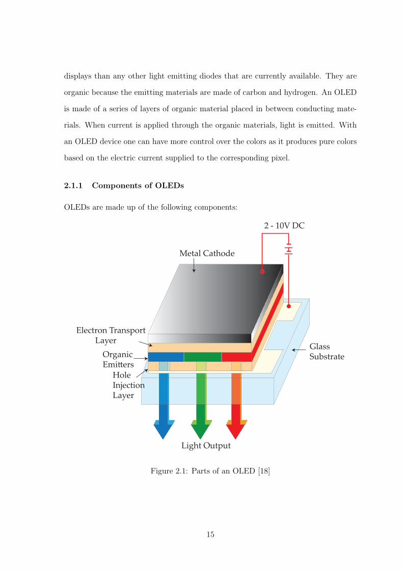
2.1.1 Components of OLEDs
OLEDs are made up of the following components:
Metal Cathode
Electron Transport Layer
Organic Emiers
HoleInjectionLayer
Light Output
GlassSubstrate
2 - 10V DC
Figure 2.1: Parts of an OLED [18]
15
• Substrate: The support material of OLEDs, which typically consists of clear
plastic, glass, foil, etc.
• Anode layer: This layer is made of materials which inject positive charges (re-
moval of electrons).
• Organic layers: These include the conducting and emissive layers.
• Cathode layer: This layer is made up of materials which release electrons into
the emission layer when current is passed through an OLED.
• Encapsulation layer: This is made of barrier material and its function is to
protect the OLED device from oxygen and moisture.
The organic layer is typically made of the hole injecting layer (HIL), also known as the
conducting layer, and the emissive layer (EL). The former transports the holes from
the anode while the latter removes electrons from the cathode layer. The emissive
layer is the layer that gets illuminated. The anode is usually made of a transparent
material whereas the cathode is usually made of a reflective material. For the anode
layer, materials with high work function are chosen. The work function of a material
is defined as the minimum energy required to remove an electron from its surface to
a point immediately outside the surface. Indium tin oxide (ITO) is commonly chosen
as anode material because of its high work function and good transparency. For the
cathode, metals with low work function are used.
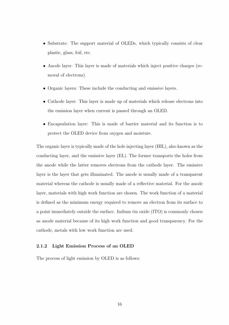
2.1.2 Light Emission Process of an OLED
The process of light emission by OLED is as follows:
16
ANODE
CATHODECATHODE CATHODECATHODECATHODE
Electrical current flows from the cathode to the anode throughthe organic layers, giving electronsto the emissive layer and removingelectrons from the conductive layer
Removing electrons from theconductive layer leaves holesthat need to be filled with the electrons in the emissive layer
The holes jump to theemissive layer and recombinewith the electrons. As the electrons drop into holes,they release their extra energy as light.
1
2
3
LightPhoton
OLED Creating Light
Conductive Layer
Emissive Layer
Electron
Figure 2.2: Light Emission Process of OLED [19]
1. Voltage is applied across the OLED by a power supply.
2. There is a flow of electric current from the cathode to the anode. The cathode
layer releases electrons to the emissive layer whereas the anode layer remove
electrons from the organic molecules of the conductive layer.
3. The electrons from the cathode layer move to fill up the electron hole created
in the conductive layer and this movement of electrons releases energy in the
form of photons which are emitted as light.
17
4. The type of organic molecules present in the OLED determines the color of
light, and the intensity of light depends on the amount of electric current that
is passed through the device.
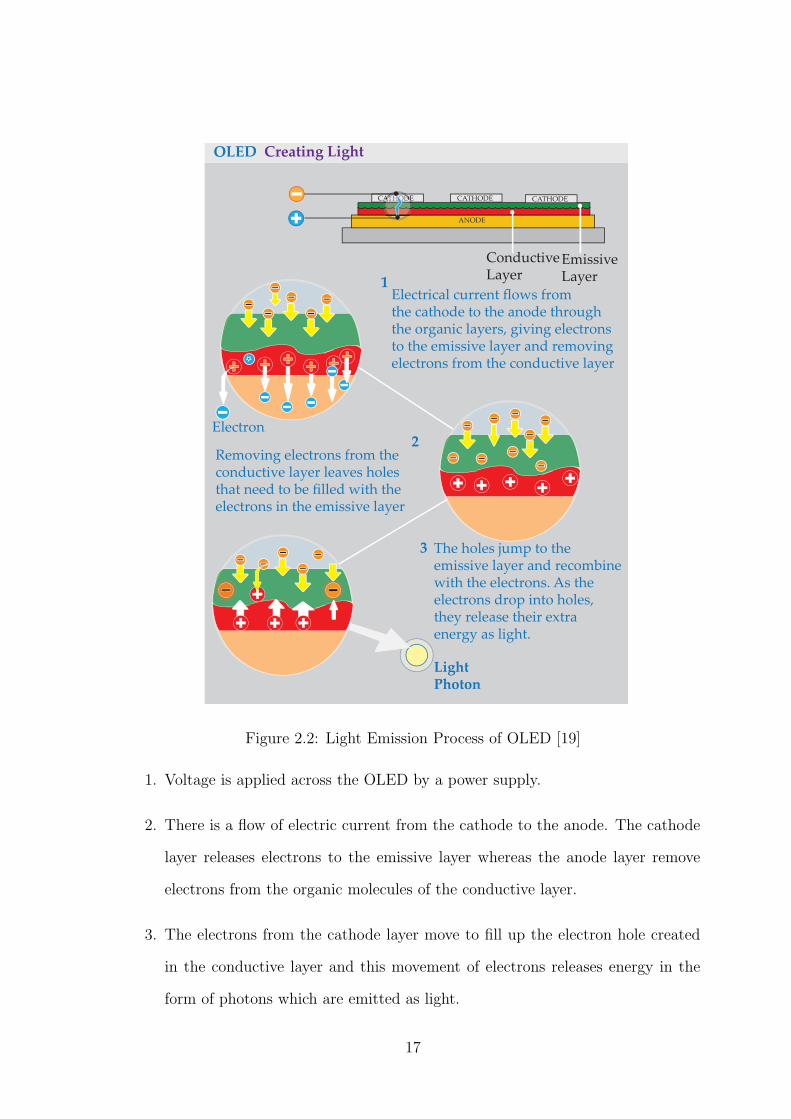
2.1.3 Methods of Deposition of Materials for Different OLED Layers
OLEDs can be fabricated in many ways. Different methods can be used to deposit
the materials to form layers of an OLED device. The deposition methods employed
depend on the factors such as the layer being deposited, materials, thickness of the
layers, resolution of the pixels, etc. Some of the methods used to deposit materials
to form the different layers of the OLED device are as follows:
Vacuum
Shadow Mask
Substrate holder
Organic Materials SourcesHeaters
Figure 2.3: Vacuum Deposition Method [20]
• Vacuum deposition or vacuum thermal evaporation (VTE): This process in-
volves heating the organic material in a vacuum chamber so that it condenses
18
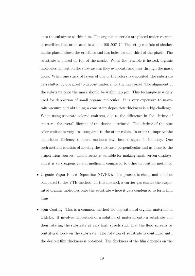
onto the substrate as thin film. The organic materials are placed under vacuum
in crucibles that are heated to about 100-500o C. The setup consists of shadow
masks placed above the crucibles and has holes for one-third of the pixels. The
substrate is placed on top of the masks. When the crucible is heated, organic
molecules deposit on the substrate as they evaporate and pass through the mask
holes. When one stack of layers of one of the colors is deposited, the substrate
gets shifted by one pixel to deposit material for the next pixel. The alignment of
the substrate onto the mask should be within ±5 µm. This technique is widely
used for deposition of small organic molecules. It is very expensive to main-
tain vacuum and obtaining a consistent deposition thickness is a big challenge.
When using separate colored emitters, due to the difference in the lifetime of
emitters, the overall lifetime of the device is reduced. The lifetime of the blue
color emitter is very less compared to the other colors. In order to improve the
deposition efficiency, different methods have been designed in industry. One
such method consists of moving the substrate perpendicular and as close to the
evaporation sources. This process is suitable for making small screen displays,
and it is very expensive and inefficient compared to other deposition methods.
• Organic Vapor Phase Deposition (OVPD): This process is cheap and efficient
compared to the VTE method. In this method, a carrier gas carries the evapo-
rated organic molecules onto the substrate where it gets condensed to form thin
films.
• Spin Coating: This is a common method for deposition of organic materials in
OLEDs. It involves deposition of a solution of material onto a substrate and
then rotating the substrate at very high speeds such that the fluid spreads by
centrifugal force on the substrate. The rotation of substrate is continued until
the desired film thickness is obtained. The thickness of the film depends on the
19
speed of rotation of the substrate, concentration of the solution, viscosity and
surface tension of the solution, etc. This method can be used to manufacture
small OLEDs, but it cannot be scaled to manufacture OLEDs in rolled form.
• Magnetic Sputtering: This method is commonly used for deposition of thin film
materials. Sputtering is a process where atoms are ejected from a target material
when it is bombarded with high energy particles. Magnetic sputtering involves
applying high power to a magnetron which results in a very high negative voltage
on the target. This causes positive ions to move toward the target at very high
speeds. When the high speed ions hit the target material and if the colliding
energy is greater than the binding energy of the atoms in the target material,
atoms will be released from the target material which can be directed onto a
substrate. This method can be used for deposition of organic materials onto
OLEDs in RTR form.
• Lift-up Soft Lithographic Technique: This method is used to pattern the anode
layers deposited on the substrate. It can be used over a large area and is known
to provide good control over the thickness of the layer on the substrate. It
involves a mold with a protruding shape brought in conformal contact with the
layer for few seconds and then removed. The material in its aqueous state will
be adhered to the mold and leaves the substrate resulting in a required pattern
of the layer on the substrate.
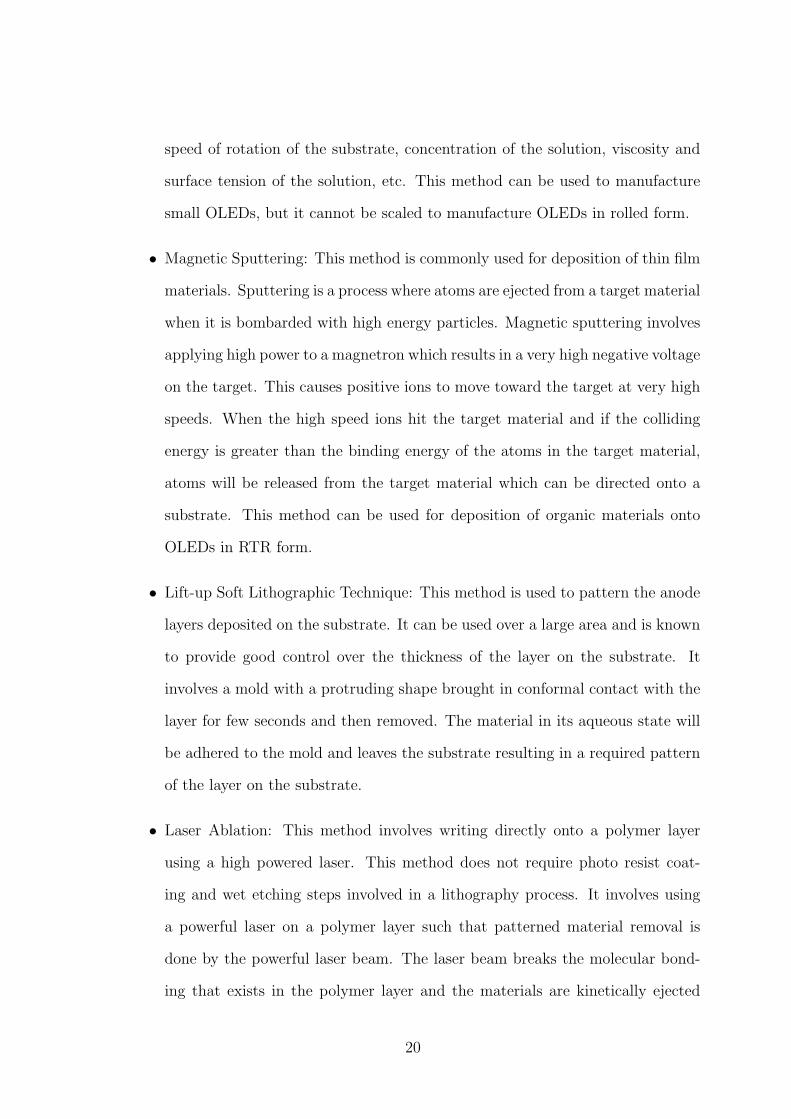
• Laser Ablation: This method involves writing directly onto a polymer layer
using a high powered laser. This method does not require photo resist coat-
ing and wet etching steps involved in a lithography process. It involves using
a powerful laser on a polymer layer such that patterned material removal is
done by the powerful laser beam. The laser beam breaks the molecular bond-
ing that exists in the polymer layer and the materials are kinetically ejected
20
upon removal. The polymer chains will be broken into chains of lower molec-
ular weight along with liberation of gases like carbon, carbon monoxide, etc.,
which get ejected from the surface at supersonic velocities. When these gases
are released at such speeds, they carry the solid particles of the polymer along
with them. The amount of material removed can be controlled by adjusting
the wavelength, energy density, and the pulse width of the laser beam used for
ablation. This process is faster than reactive ion etching and produces cleaner
lines than thermal and mechanical drilling which are the traditional methods
of material removal in electronic packaging. When using this method for mul-
tilayered devices, short laser pulses are better than long pulses mainly because
they reduces the heat in the affected zone. Compared to a thermal ablation
process, this method produces a clean surface around the ablation region with
minimal material build up whereas the thermal ablation process creates a large
heat affected zone with melted material appearing around the ablation region.
• Ink-jet printing: This is a process where the organic material is sprayed onto the
substrate in a manner similar to the spraying of ink onto paper during printing.
Using this method, OLED layers can be deposited in RTR form which reduces
the production cost by a considerable amount. The equipment consists of a
substrate that is patterned and has polyamide banks surrounding the pixel area.
Ink-jet nozzles are placed above the substrate and consist of ink solution for
deposition. The ink solution is dispensed on the substrate through the nozzles
and great care must be taken to position the ink-jet tip as a slight difference
in the angle will cause considerable error. A high speed camera is used to
monitor the ink droplet to ensure proper working of the nozzle. The banks
form a well around the pixel area and are water repellent. The pixel area is
made hydrophilic so that any sticking of the droplet onto the bank is prevented.
21
Irradiation
Absorbtion
Bond-Breaking
Ablation
Pulsed LaserBeam
Mask
ProjectionLens
OrganicPolymer
Figure 2.4: Laser Ablation [21]
Once the ink gets deposited, it is dried to form the film. The challenges that are
incurred in this method are the pre-patterning of the substrate and obtaining a
uniform pattern after drying of the ink droplets on the substrate. This process
is highly suitable for the manufacture of large screen displays using polymer
organic molecules. It has the advantage of not having any vacuum chamber and
mask patterning system. It has the advantage of low temperature processing
and results in a low cost manufacturing system. It also has the advantage of
depositing a controlled pattern of polymers on the substrate which would be
very beneficial for full color displays. This method results in low consumption
22
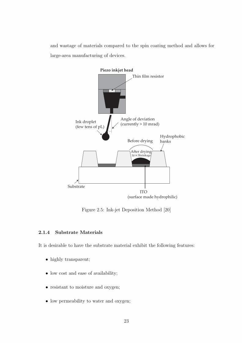
and wastage of materials compared to the spin coating method and allows for
large-area manufacturing of devices.
Piezo inkjet head
Hydrophobicbanks
Angle of deviation(currently > 10 mrad)
Thin film resistor
Ink droplet(few tens of pL)
Substrate
ITO(surface made hydrophilic)
Before drying
A!er drying50 Shrinkage
Figure 2.5: Ink-jet Deposition Method [20]
2.1.4 Substrate Materials
It is desirable to have the substrate material exhibit the following features:
• highly transparent;
• low cost and ease of availability;
• resistant to moisture and oxygen;
• low permeability to water and oxygen;
23
• resistant to chemical attack and dimensionally stable under different cycles of
heating processes;
• able to withstand high temperature conditions (as much as 250o C);
• coefficient of thermal expansion must be similar to the layer being coupled with;
any mismatch will result in cracking and high residual stresses during thermal
cycling;
Certain plastics tend to shrink when they are cooled after high temperature processes.
This can be avoided by pre-annealing the film under high temperature and using
minimal web tension when they are rolled. Materials should be flexible enough to
be rolled. Flexibility of the materials will enable them to be manufactured in sheet
form, which would reduce the overall cost of manufacturing. Most common materials
used for the substrate are glass, plastic, and stainless steel.
Glass: Glass has been used as the standard substrate material for OLEDs that
are not required to be flexible. It has good optical properties, smooth surface
finish and low coefficient of thermal expansion. A major disadvantage of glass
is that it is susceptible to breaking and tends to crack near the edges if it is not
handled properly. But this problem can be rectified by coating the glass surface
and edges with a thin polymer layer. There is also a process called ion exchange
where the glass can be strengthened so that breakage can be reduced, but this
results in a compression on the external surface and tension in the interior
surface of the glass. Using glass as a substrate has the advantage of amended
visual appearance, light weight and thinner displays but also faces the challenges
of sagging, vibration and edge finishing. There has always been a myth that
glass is weaker if its thinner, but glass breakage is dependant on external factors
such as applied stress, environmental condition, impact condition, etc. Many
24
researchers have been working on the manufacture of thin glass films that can
be rolled in order to reduce the cost of manufacturing.
Plastics: Due to low cost and toughness, plastics have been a major contender
for substrate materials. At high temperature condition cycles, these materials
undergo change in their physical and mechanical properties. When they reach
glass transition temperature, they start to flow as liquid and undergo a great
change in dimensional stability. They are permeable to water and oxygen, and
hence require barrier layers. The plastic polymeric materials are transparent
and can be processed in web form for the manufacture of flexible OLEDs.
Stainless steel: This is suitable as a substrate layer where optical transparency is
not required. They are highly impermeable to moisture and oxygen and are
flexible, durable, and have much better dimensional stability than plastic under
high thermal conditions. They are proven to be a successful substrate material
for top emitting active matrix organic light emitting displays (AMOLED) with
TFT circuitry. This material has a rough surface and have to be turned into
a smooth flat surface by coating a planarization layer on top of it; application
of such coatings make them non-conductive. These substrates are very flexible
and a promising candidate for the manufacture of OLED devices using RTR
manufacturing.
2.1.5 Color Generation
Color generation is an important factor in OLED displays. Colors can be generated
mainly in three different ways as described in the following:
• Use of red, green and blue individual pixels (see Fig. 2.6 (a)): Three different
color emitters are used for red, green and blue colors. This method is power
efficient and the production cost is low. The main problem associated with it
25
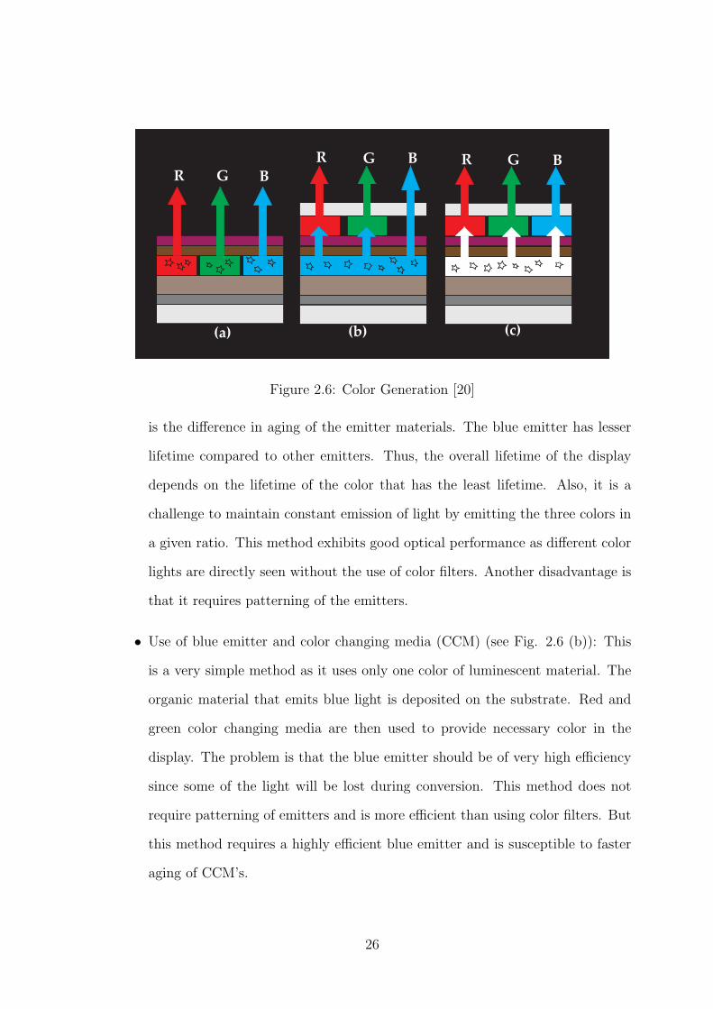
RR
GG
B
R G B B
(a) (c)(b)
Figure 2.6: Color Generation [20]
is the difference in aging of the emitter materials. The blue emitter has lesser
lifetime compared to other emitters. Thus, the overall lifetime of the display
depends on the lifetime of the color that has the least lifetime. Also, it is a
challenge to maintain constant emission of light by emitting the three colors in
a given ratio. This method exhibits good optical performance as different color
lights are directly seen without the use of color filters. Another disadvantage is
that it requires patterning of the emitters.
• Use of blue emitter and color changing media (CCM) (see Fig. 2.6 (b)): This
is a very simple method as it uses only one color of luminescent material. The
organic material that emits blue light is deposited on the substrate. Red and
green color changing media are then used to provide necessary color in the
display. The problem is that the blue emitter should be of very high efficiency
since some of the light will be lost during conversion. This method does not
require patterning of emitters and is more efficient than using color filters. But
this method requires a highly efficient blue emitter and is susceptible to faster
aging of CCM’s.
26
• Use of white emitter and color filters (see Fig. 2.6 (c)): In this method, two
or more organic materials are combined to generate white light which is then
converted to red, green, and blue colors using color filters. This method ex-
periences loss in intensity of light as color filters are used. It does not require
patterning of emitter and does not involve problems with differential aging of
the emitters. This method is power inefficient and for efficient working of the
device, a highly efficient white emitter is necessary.
2.1.6 OLED Emission Types
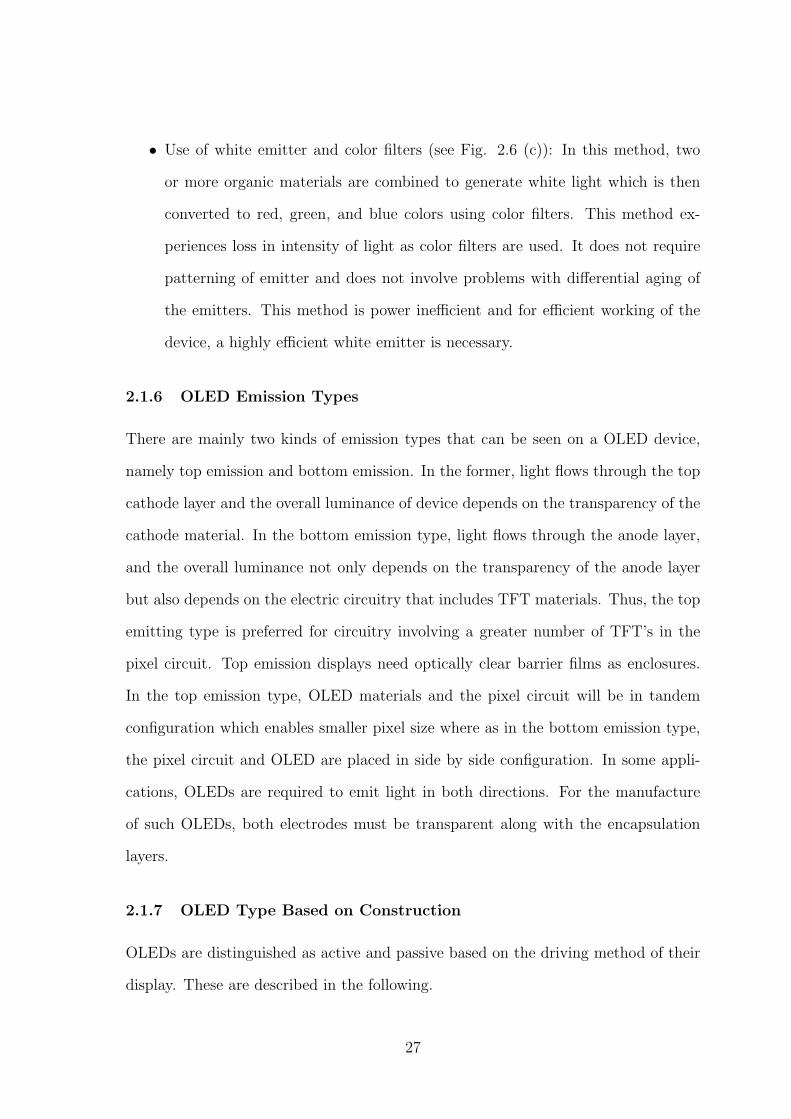
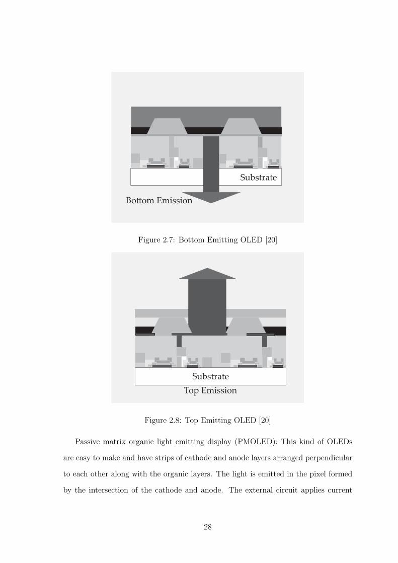
There are mainly two kinds of emission types that can be seen on a OLED device,
namely top emission and bottom emission. In the former, light flows through the top
cathode layer and the overall luminance of device depends on the transparency of the
cathode material. In the bottom emission type, light flows through the anode layer,
and the overall luminance not only depends on the transparency of the anode layer
but also depends on the electric circuitry that includes TFT materials. Thus, the top
emitting type is preferred for circuitry involving a greater number of TFT’s in the
pixel circuit. Top emission displays need optically clear barrier films as enclosures.
In the top emission type, OLED materials and the pixel circuit will be in tandem
configuration which enables smaller pixel size where as in the bottom emission type,
the pixel circuit and OLED are placed in side by side configuration. In some appli-
cations, OLEDs are required to emit light in both directions. For the manufacture
of such OLEDs, both electrodes must be transparent along with the encapsulation
layers.
2.1.7 OLED Type Based on Construction
OLEDs are distinguished as active and passive based on the driving method of their
display. These are described in the following.
27
Substrate
Boom Emission
Figure 2.7: Bottom Emitting OLED [20]
Substrate
Top Emission
Figure 2.8: Top Emitting OLED [20]
Passive matrix organic light emitting display (PMOLED): This kind of OLEDs
are easy to make and have strips of cathode and anode layers arranged perpendicular
to each other along with the organic layers. The light is emitted in the pixel formed
by the intersection of the cathode and anode. The external circuit applies current
28
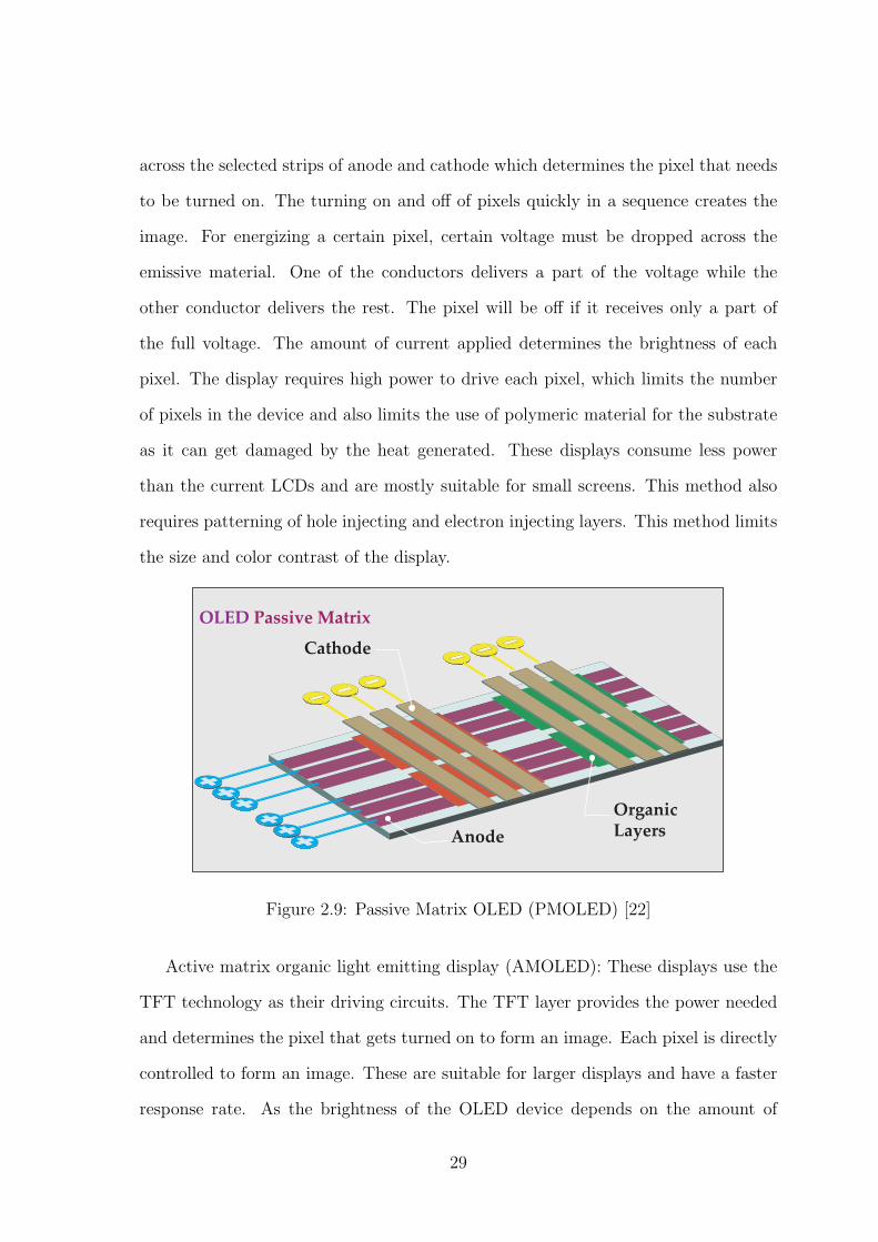
across the selected strips of anode and cathode which determines the pixel that needs
to be turned on. The turning on and off of pixels quickly in a sequence creates the
image. For energizing a certain pixel, certain voltage must be dropped across the
emissive material. One of the conductors delivers a part of the voltage while the
other conductor delivers the rest. The pixel will be off if it receives only a part of
the full voltage. The amount of current applied determines the brightness of each
pixel. The display requires high power to drive each pixel, which limits the number
of pixels in the device and also limits the use of polymeric material for the substrate
as it can get damaged by the heat generated. These displays consume less power
than the current LCDs and are mostly suitable for small screens. This method also
requires patterning of hole injecting and electron injecting layers. This method limits
the size and color contrast of the display.
Cathode
OrganicLayersAnode
OLED Passive Matrix
Figure 2.9: Passive Matrix OLED (PMOLED) [22]
Active matrix organic light emitting display (AMOLED): These displays use the
TFT technology as their driving circuits. The TFT layer provides the power needed
and determines the pixel that gets turned on to form an image. Each pixel is directly
controlled to form an image. These are suitable for larger displays and have a faster
response rate. As the brightness of the OLED device depends on the amount of
29
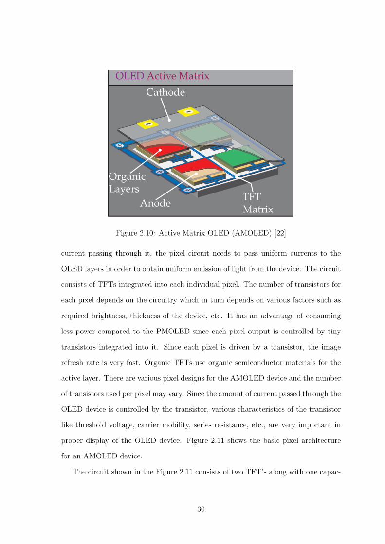
TFT Matrix
OrganicLayers
Anode
Cathode
OLED Active Matrix
Figure 2.10: Active Matrix OLED (AMOLED) [22]
current passing through it, the pixel circuit needs to pass uniform currents to the
OLED layers in order to obtain uniform emission of light from the device. The circuit
consists of TFTs integrated into each individual pixel. The number of transistors for
each pixel depends on the circuitry which in turn depends on various factors such as
required brightness, thickness of the device, etc. It has an advantage of consuming
less power compared to the PMOLED since each pixel output is controlled by tiny
transistors integrated into it. Since each pixel is driven by a transistor, the image
refresh rate is very fast. Organic TFTs use organic semiconductor materials for the
active layer. There are various pixel designs for the AMOLED device and the number
of transistors used per pixel may vary. Since the amount of current passed through the
OLED device is controlled by the transistor, various characteristics of the transistor
like threshold voltage, carrier mobility, series resistance, etc., are very important in
proper display of the OLED device. Figure 2.11 shows the basic pixel architecture
for an AMOLED device.
The circuit shown in the Figure 2.11 consists of two TFT’s along with one capac-
30
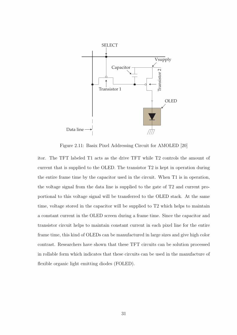
Data line
SELECT
Transistor 1 Tra
nsi
sto
r 2
OLED
Capacitor
Vsupply
Figure 2.11: Basix Pixel Addressing Circuit for AMOLED [20]
itor. The TFT labeled T1 acts as the drive TFT while T2 controls the amount of
current that is supplied to the OLED. The transistor T2 is kept in operation during
the entire frame time by the capacitor used in the circuit. When T1 is in operation,
the voltage signal from the data line is supplied to the gate of T2 and current pro-
portional to this voltage signal will be transferred to the OLED stack. At the same
time, voltage stored in the capacitor will be supplied to T2 which helps to maintain
a constant current in the OLED screen during a frame time. Since the capacitor and
transistor circuit helps to maintain constant current in each pixel line for the entire
frame time, this kind of OLEDs can be manufactured in large sizes and give high color
contrast. Researchers have shown that these TFT circuits can be solution processed
in rollable form which indicates that these circuits can be used in the manufacture of
flexible organic light emitting diodes (FOLED).
31
2.1.8 OLED Type Based on the Material Type
Based on the type of materials in the organic layer, OLEDs can be divided into
small molecule OLEDs (SMOLEDs) and polymer based OLEDs (PLEDs). They are
described as follows:
• Small molecule OLEDs consist of materials with low molecular weight. They
are deposited mostly by a vacuum thermal evaporation process which is usu-
ally a dry process. Vacuum deposition is a very expensive method and there-
fore SMOLEDs are suitable for small screens and small object displays. The
main disadvantage of using small molecule OLEDs is in their manufacturing
process as they require extra materials like phosphorus to enhance their per-
formance. Devices formed from small molecule materials allow more layer en-
gineering and have more advanced architecture than the PLED devices. Small
molecule OLEDs are very common and are used in applications such as cell
phones, digital cameras, etc.
• PLEDs are made of long polymeric organic chains and are deposited by ink-jet
or spin cast methods which is usually a wet process. PLEDs can be made by
solution based methods in sheet form and are suitable for large screen displays.
PLEDs can be produced in large quantities using ink-jet printing methods but
current trends show that they are deficient in terms of efficiency and lifetime.
2.1.9 Differences Between Inorganic LEDs and OLEDs
Inorganic LEDs have high brightness point sources and are more like incandescent
light devices whereas organic LEDs are area extended sources with wide angle and
are more like fluorescent light devices. Inorganic LEDs find applications in spot light
areas like flashlights, traffic lights, etc., whereas OLEDs find application in diffuse
lighting such as signs, back lights, television, etc.
32
2.1.10 Differences Between Dry Coated and Wet Coated OLEDs
In dry-coated LEDs, high vacuum is used to evaporate the organic layers whereas in
the case of wet-coated technology organic layers are printed with solution. The former
are made of more layers whereas the latter are made of fewer layers. It is difficult to
scale dry coated LEDs to a large area as they are made of small molecules, whereas
wet coated ones are made of larger polymers or molecules and can be manufactured
in a large area.
2.1.11 Flexible OLEDs
OLEDs that can be manufactured in rollable form are termed as flexible OLEDs. A
crucial requirement for these kinds of OLEDs is that the substrate must be flexible
which means that it must be bendable, flexed and also rollable any number of times
without degrading its performance. All the materials that are laid on top of the sub-
strate must also be flexible. For transmissive displays, opaque materials for substrate
cannot be used as they should be able to transmit light through them.
• Flexible substrate materials: Research is currently active in the testing of suit-
able materials for substrates that will be flexible, economical and compatible
with the other layer materials of OLEDS. The most common materials that
have been used as of now are polymeric films, stainless steel foils and ultra-thin
flexible glass. Each of them have unique properties which are suitable for certain
applications. The ultra-thin flexible glasses cannot be processed in RTR form
while stainless steel cannot be used for transparent OLEDs. Metal foils are very
expensive and hence cannot be used for large size displays. Polymeric films are
best suited to be manufactured in rollable form but they have the disadvan-
tage of not being resistant to oxygen and moisture. Thus, proper encapsulation
is required with flexible barrier materials when polymeric materials are being
used for the substrate. The polymeric materials chosen for substrate must
33
have very high mechanical, thermal and dimensional stability, high resistance
to chemical materials, low coefficient of thermal expansion, high optical trans-
parency, very smooth surface along with being impermeable to oxygen and mois-
ture. The most common materials used for flexible substrates are polyethylene
terephthalate (PET), polyethylene naphthalate (PEN), polyamide, polycarbon-
ate (PC), cyclic olefin copolymer (COC), polyamide/organoclay nanocompos-
ite (PI/OMMT), poly ethersulphone (PES), poly dimenthylsiloxane (PDMS),
polyvinylidene difluoride (PVDF), polyetheretherketone (PEEK), etc. Table
2.1 and Table 2.2 show some of the important properties of these materials.
Thermal stability of the plastic substrate is also an important requirement as the
substrate is subjected to high temperature processes during coating of barrier
materials, electrode deposition, patterning, TFT deposition, etc. Mechanical
properties of the materials are also an important criteria in the selection of the
materials for the substrate. The flexibility of the device depends on factors such
as thickness of the device, materials used for each of the layers, arrangement
of the layers, mechanical properties of materials, etc. Inorganic materials are
generally brittle and require some treatment to improve their flexibility before
being used for the manufacture of FOLEDs.
• Flexible electrode materials: These are the materials that are required for pas-
sage of electrical signals between the power supply, driver circuitry, and display
pixels. Selection of these materials is important as they provide the necessary
conduit by which electric signals are passed that will result in the display of an
image in applications such as televisions, display screens, etc. Some of the ma-
terials that are available for electrodes include Indium Tin Oxide (ITO), carbon
nanotube films, polymers, thin metal films, hybrid organic-inorganic films, etc.
– ITO: This is the most commonly used material for the electrode layer as
34
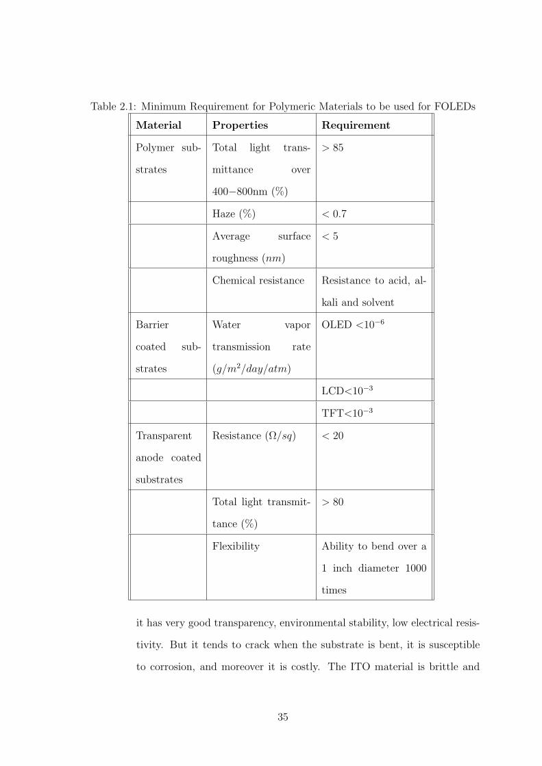
Table 2.1: Minimum Requirement for Polymeric Materials to be used for FOLEDs
Material Properties Requirement
Polymer sub-
strates
Total light trans-
mittance over
400−800nm (%)
> 85
Haze (%) < 0.7
Average surface
roughness (nm)
< 5
Chemical resistance Resistance to acid, al-
kali and solvent
Barrier
coated sub-
strates
Water vapor
transmission rate
(g/m2/day/atm)
OLED <10−6
LCD<10−3
TFT<10−3
Transparent
anode coated
substrates
Resistance (Ω/sq) < 20
Total light transmit-
tance (%)
> 80
Flexibility Ability to bend over a
1 inch diameter 1000
times
it has very good transparency, environmental stability, low electrical resis-
tivity. But it tends to crack when the substrate is bent, it is susceptible
to corrosion, and moreover it is costly. The ITO material is brittle and
35
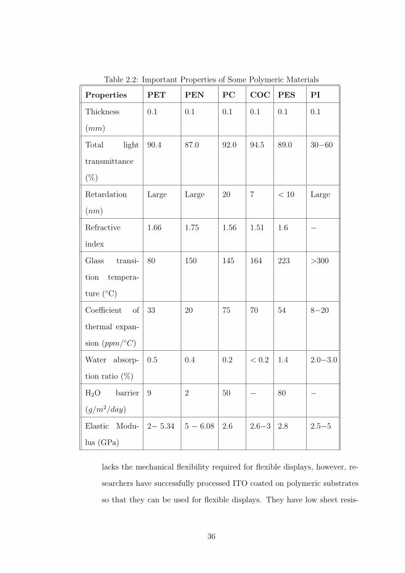
Table 2.2: Important Properties of Some Polymeric Materials
Properties PET PEN PC COC PES PI
Thickness
(mm)
0.1 0.1 0.1 0.1 0.1 0.1
Total light
transmittance
(%)
90.4 87.0 92.0 94.5 89.0 30−60
Retardation
(nm)
Large Large 20 7 < 10 Large
Refractive
index
1.66 1.75 1.56 1.51 1.6 −
Glass transi-
tion tempera-
ture (C)
80 150 145 164 223 >300
Coefficient of
thermal expan-
sion (ppm/C)
33 20 75 70 54 8−20
Water absorp-
tion ratio (%)
0.5 0.4 0.2 < 0.2 1.4 2.0−3.0
H2O barrier
(g/m2/day)
9 2 50 − 80 −
Elastic Modu-
lus (GPa)
2− 5.34 5 − 6.08 2.6 2.6−3 2.8 2.5−5
lacks the mechanical flexibility required for flexible displays, however, re-
searchers have successfully processed ITO coated on polymeric substrates
so that they can be used for flexible displays. They have low sheet resis-
36
tance and are more environmentally stable compared to some other elec-
trode materials. Oxygen plasma treatment of an ITO material enhances
the hole injection property, and thus makes it more suitable for use as an
anode material.
– Indium Zinc Oxide (IZO): These materials show good electrical and me-
chanical properties like ITO. They do not require substrate heating or any
post-deposition annealing process as required for the deposition of ITO.
Similar to ITO, IZO is brittle and thus it is a challenge for using it in
flexible display applications.
– Carbon Nanotubes: These materials are formed from graphite sheets and
have excellent thermal, mechanical and electrical properties due to which
these materials are finding application in thin electronic applications. They
have high elastic modulus and are very strong compared to other materials
used for the electrode layer. They can be processed in vacuum at very high
temperatures without losing their thermal stability. They have very high
thermal conductivity and electrical properties. But researchers have shown
that their efficiency is less compared to ITO.
– Polymer Materials: Most of the polymeric materials are insulating in na-
ture but there are conductive polymers that have good electrical proper-
ties, which can be easily flexed and have very high optical transparency.
They also have the ability to be solution processed at room tempera-
ture. One of the most used conductive polymeric materials is poly (3,4-
ethylenedioxythiophene), poly (styrene sulfonate) which is also known as
PEDOT:PSS. There are other conducting polymers that can be used for
the anode layer which have better properties than the ITO material. PE-
DOT:PSS is one of those conducting polymers which appears to be a good
material to be used for the electrode mainly because of its excellent ther-
37
mal stability and high transparency than the other conducting polymers.
It also has the advantage of easy deposition, less surface roughness, less
cost compared to ITO material. Even though it has lower transparency
than the ITO material, this problem can be resolved by adding dimethyl-
sulfoxide (DMSO) to an aqueous solution of PEDOT:PSS material. It has
an advantage that it can be easily solution coated onto substrate mate-
rials. PEDOT:PSS is also used as a material for HIL as it improves the
electromechanical performance of an ITO coated poly ethylene terephtha-
late (PET) substrate.
There are several challenges faced in the manufacture of flexible electronics. Two of
the main challenges for flexible electronic devices are obtaining a suitable thin barrier
layer for polymeric substrates and improving the flexibility of brittle inorganic films
like ITO. Polymeric substrates must be encapsulated with flexible barrier materials
that would prevent permeation of oxygen and moisture which otherwise may cause
degradation of the device. All OLEDs must be sealed on the top and bottom sides of
the device which is termed as encapsulation. Usually, OLEDs have been encapsulated
using a metal in an inert atmosphere such as oxygen or nitrogen and using calcium
oxide or barium oxides to stop any water diffusing into the device. But this kind of
encapsulation is not applicable for flexible OLEDs. Flexible OLEDs can be encap-
sulated mainly in two ways, one is by using barrier-coated polymer substrate which
provides a multilayer structure and has the advantage of providing a mechanically
robust device and the second method is by coating a thin-film multilayer directly on
the device. For transparent devices, these barrier materials must be transmissive in
nature along with being flexible. The common materials used for forming barrier
layers are aluminium, aluminium oxides or silicon oxides.
The selection of barrier materials is important for successful manufacture of an
OLEDs. It is found that for an OLED with a lifetime of 10,000 hours or more, water
38
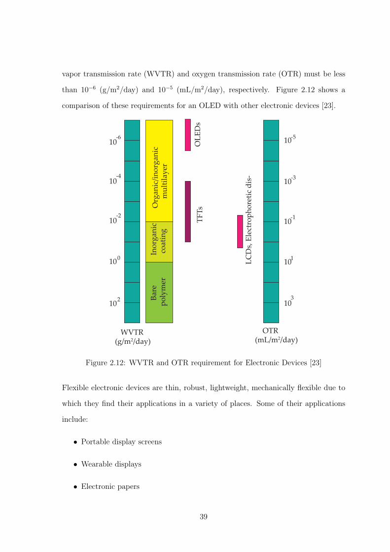
vapor transmission rate (WVTR) and oxygen transmission rate (OTR) must be less
than 10−6 (g/m2/day) and 10−5 (mL/m2/day), respectively. Figure 2.12 shows a
comparison of these requirements for an OLED with other electronic devices [23].
10
10
10
10
10
1
-5
-3
-1
3
B
are
po
lym
er
Ino
rgan
ic
c
oat
ing
Org
anic
/in
org
anic
m
ult
ilay
er
TF
Ts
OL
ED
s
LC
Ds,
Ele
ctro
ph
ore
tic
dis
-
102
10
10
10
10
-6
-4
-2
0
WVTR(g/m2/day)
OTR(mL/m2/day)
Figure 2.12: WVTR and OTR requirement for Electronic Devices [23]
Flexible electronic devices are thin, robust, lightweight, mechanically flexible due to
which they find their applications in a variety of places. Some of their applications
include:
• Portable display screens
• Wearable displays
• Electronic papers
39
• Decorative lighting
• Flexible window panes
• Automobile accessories
• Television displays
• Cameras, mobile phone displays, etc.
2.1.12 Advantages and Disadvantages of OLED Devices
Advantages:
1. In OLEDs, the organic layers are plastic and hence are lighter, thinner and
flexible compared to the crystalline layers of LED or LCD.
2. OLEDs are brighter than LEDs. The substrate used to support OLEDs can
be made of plastic rather than the glass substrates used for LEDs. The glass
substrate absorbs light, but that problem does not exist in OLED.
3. OLEDs consume less power than LCDs since there is no back lighting in OLEDs.
This is one of the major advantages of OLED over LCD. OLED being emissive,
can be turned off to remain completely dark whereas LCD being transmissive
does not allow for the complete blocking of its backlight. This reduces the power
required and also the number of layers of the substrate required which would
make it thin and more efficient. LCD consumes the same power regardless of
the image being fully black or white but OLEDs power consumption depends
on the image being displayed. Darker images consume less power while white
images consume more power.
4. OLEDs have a wider viewing angle of upto 170 degrees and can operate at very
low voltage ranges (2−10 volts). Thus the image can be seen from any angle
clearly without having problems of blurring or color contrast.
40
5. OLEDs have a better contrast and faster refresh rate, as a result motion blur
is minimized.
6. OLEDs are flexible and can be manufactured in large quantities using RTR
manufacturing. They can be produced in different shapes. Very thin and trans-
parent OLEDs can be prepared.
7. OLEDs have vast color range compared to the other currently available displays.
8. As they are flexible, they are not affected by shock or twisting forces.
9. They can work in a much greater operating temperature range than LCDs.
10. In the case of AMOLEDs, there is no backlighting and each pixel can be turned
on by the TFT matrix. Thus there are no limitations to the resolution, pixel
count and size of the display.
11. Flexible OLED displays can be rolled, bent, conformed to any shape. Such
properties can be used to produce portable rollable displays, irregular shaped
displays, wristband displays, etc.
Disadvantages:
1. It is currently expensive to manufacture OLEDs. But many companies are
trying to develop RTR technologies to manufacture OLEDs in web form which
would reduce the cost of manufacturing to a great extent.
2. OLEDS have a problem of operating in direct sunlight because of their emissive
nature. Since they are emissive, when they are viewed under direct sunlight,
they face readability problems. Research is being actively pursued to resolve
this problem.
3. Indium is a rare earth element and thus expensive to mine and difficult to
recycle. Low temperature conditions must be accommodated when using ITO
41
with glass substrate in order to obtain low sheet resistance and high optical
properties. ITO may also undergo cracking under tensile strain when it is
placed on a polymeric substrate which would result in failure of the flexible
display.
4. OLEDs tend to get dimmer within several hours of working. The problem is
mainly with the blue component of the OLED that tends to fail within 5000
hours of working. Research is being actively pursued to resolve this problem.
5. Most of the OLED materials are chemically unstable in the presence of moisture
and oxygen which can lead to the formation of dark spots in the display. Proper
barrier encapsulation should be provided in order to overcome this issue.
2.1.13 Challenges Faced in Manufacturing of OLEDs
The main challenge is in manufacturing of large size OLED displays with reasonable
cost. Material lifetime and efficiency are also a matter of concern. The overall lifetime
of the OLED device is calculated as the mean time to half brightness. Due to the
difference in aging of the different color emitters, the overall lifetime of the device is
greatly reduced. Initial investments in the manufacturing of OLEDs have been high
and this should be reduced in order to compete with other technologies. Depositing
the organic molecules to the substrate to obtain the different colored pixels has been
a major challenge faced by the manufacturers. Small molecule based OLEDs have
been experiencing problems such as catastrophic failure, dark-spot degradation, and
intrinsic degradation. By using adequate methods of fabrication, the first two prob-
lems can be solved but the third problem has been of considerable challenge to the
OLED manufacturers. Also, the lifetime of organic materials drop significantly with
increase in temperature. This will be a major problem mainly when choosing the
organic materials for the television displays, computer screens, etc.
42
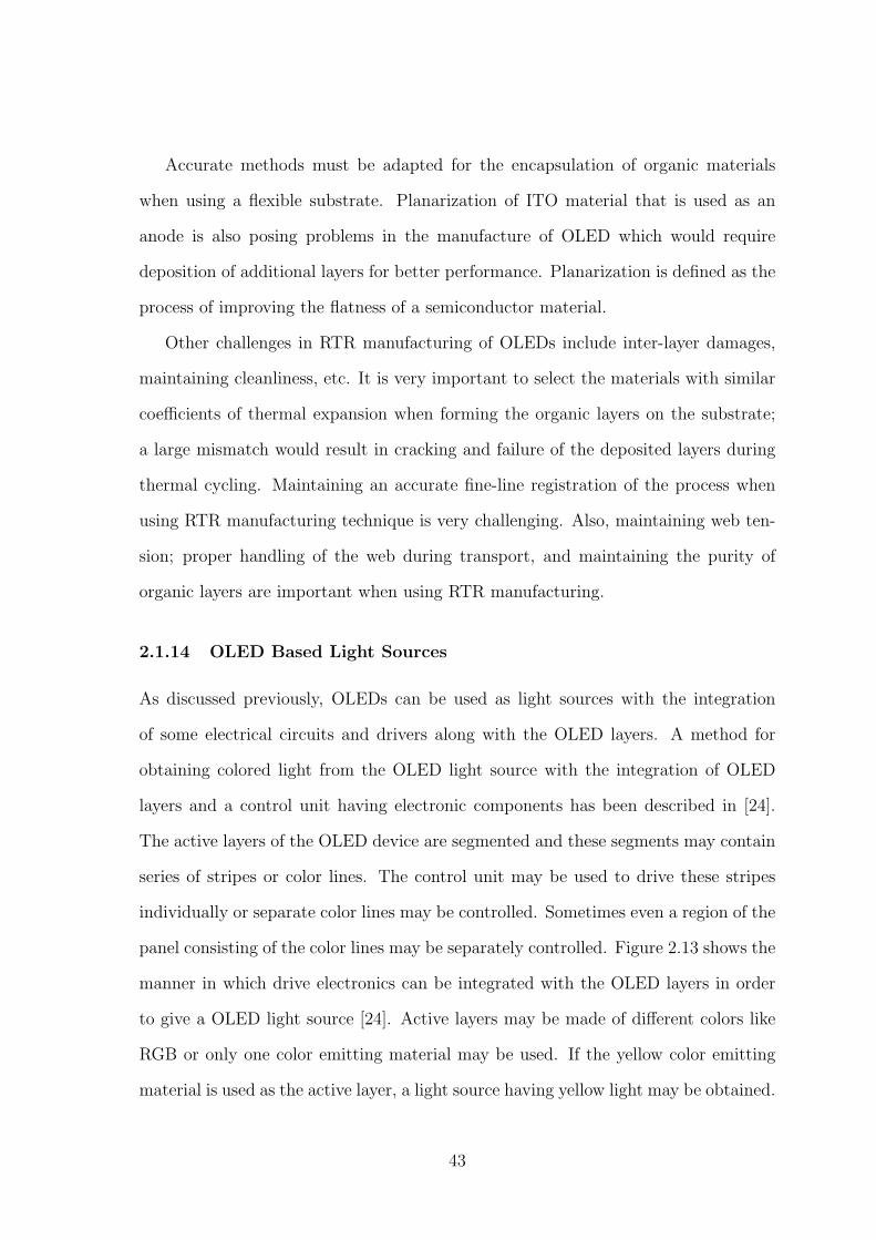
Accurate methods must be adapted for the encapsulation of organic materials
when using a flexible substrate. Planarization of ITO material that is used as an
anode is also posing problems in the manufacture of OLED which would require
deposition of additional layers for better performance. Planarization is defined as the
process of improving the flatness of a semiconductor material.
Other challenges in RTR manufacturing of OLEDs include inter-layer damages,
maintaining cleanliness, etc. It is very important to select the materials with similar
coefficients of thermal expansion when forming the organic layers on the substrate;
a large mismatch would result in cracking and failure of the deposited layers during
thermal cycling. Maintaining an accurate fine-line registration of the process when
using RTR manufacturing technique is very challenging. Also, maintaining web ten-
sion; proper handling of the web during transport, and maintaining the purity of
organic layers are important when using RTR manufacturing.
2.1.14 OLED Based Light Sources
As discussed previously, OLEDs can be used as light sources with the integration
of some electrical circuits and drivers along with the OLED layers. A method for
obtaining colored light from the OLED light source with the integration of OLED
layers and a control unit having electronic components has been described in [24].
The active layers of the OLED device are segmented and these segments may contain
series of stripes or color lines. The control unit may be used to drive these stripes
individually or separate color lines may be controlled. Sometimes even a region of the
panel consisting of the color lines may be separately controlled. Figure 2.13 shows the
manner in which drive electronics can be integrated with the OLED layers in order
to give a OLED light source [24]. Active layers may be made of different colors like
RGB or only one color emitting material may be used. If the yellow color emitting
material is used as the active layer, a light source having yellow light may be obtained.
43
Likewise, individual color lines of the active layer having RGB color emitting material
lines may be controlled in order to obtain different shades of RGB colors. Different
shades of these colors may be controlled in order to obtain white light or any other
necessary color lighting device. In order to create a flexible light source from the
R
GB
RG
B
Light Source Area
Control Unit
Pixel Line
UserLight/Color Sensor
MicroProcessor
DriverElectronics
Fuse
Control Line
microprocessor
DRIVER
MUX
LIGHT DETECTOR
Figure 2.13: OLED Light Source [24]
OLED layers, the following materials and layers are required.
• Substrate: The substrate has to be transparent and flexible. Any of the plas-
tic material like PET, PEN, PC or semi rigid thin glass can be used for the
substrate.
• Anode: The anode material is deposited and patterned on top of the substrate.
Material such as ITO, IZO etc., may be used as the anode material.
• Bus line: An optional bus line may be deposited on top of the anode in order
44
to decrease the overall resistance of the anode stripe across the panel. This
can be of any metal or metal alloy material. This is sometimes necessary if the
resistance of the anode material is large which would require a large amount of
voltage to drive the current.
• Insulating separators: These may be deposited on top of the above mentioned
layers in order to provide proper electrical isolation. It is optional and it can
be of any insulating materials like photo resist, SiOx, SiNx, etc. These are used
to provide proper separation between the stripes of the light panel. Sometimes,
just patterning of the anode material is enough to obtain electrical isolation.
• Hole injection layer: This layer is used to complement the anode layer in hole
creation and can be made of PEDOT:PSS, Pani or any other conducting poly-
mers.
• Active layers: This layer is made of emitting material. Any material or combi-
nation of materials may be used in order to obtain specific colored light.
• Cathode layer: Finally, on top of the active layers, cathode material is deposited
which can be made of any low work function metal or alloy. The cathode layer
can be segmented similar to the anode stripes. Sometimes, only the cathode
layer may be patterned and the anode layer need not be patterned or cathode
can be deposited on top of the substrate and the anode layer may be deposited
on top of the emission layer.
The above layers are shown in the Figure 2.14. Sometimes, an insulating or electron
injection layer may be deposited between the emission layer and the cathode layer
which would supplement electron injection. For a light source, the thickness and
the resolution of the layers are larger compared to the display devices. At the light
output side of the device, a brightness enhancement layer may be laminated to the
45
substrate. As shown in Figure 2.13, the individual red, green and blue color stripes
may be directly addressed by the current source. The current to this source can be
controlled by a circuit in order to avoid excess current flows. Figure 2.13 shows a
light source area and a control unit used to control the current input to the individual
stripes of the layers. The location of the control unit depends on the demands of the
light source. It may be separately constructed or it may be integrated with the light
source layers on the same substrate. A part of the control unit may be integrated
with the light source on the substrate and the rest may be constructed separately.
The control unit consists of driver electronics, microprocessor, light sensor, etc. If
three different colors are used in order to obtain the white light, then a sensor can
be used to check the color obtained from the light panel based on the temperature
of white light required. A microprocessor can be used to obtain the signal from the
sensor based on which it can send the required control signals to the driver circuits.
Any combination of the stripes can be turned on/off and any color can be obtained
from the light source. Even a fuse can be integrated with each control line so that if
the current to that particular stripe exceeds the limit, then the fuse would blow and
would prevent failure of the entire device. The segmentation of the layers in the light
source can be done in different ways. The stripes for the segmentation can be in the
form of rows, columns or in the form of the pixels or any other shape or combination
can also be employed.
2.1.15 OLED Display Device
One of the most important application of OLEDs is in the display industry. Having
benefits of wide viewing angle, better quality, thinner display, light weight and flexi-
bility, OLED is a promising technology to replace other current technologies such as
LCDs in the field of display devices. Many researchers have described how an OLED
can be integrated with the electronic components in order to obtain a display device.
46
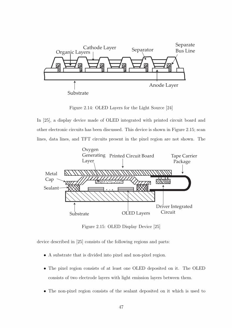
SeparatorOrganic Layers
Separate Bus Line
Anode Layer
Substrate
Cathode Layer
Figure 2.14: OLED Layers for the Light Source [24]
In [25], a display device made of OLED integrated with printed circuit board and
other electronic circuits has been discussed. This device is shown in Figure 2.15; scan
lines, data lines, and TFT circuits present in the pixel region are not shown. The
Substrate OLED Layers
Sealant
Tape Carrier Package
Driver Integrated Circuit
Printed Circuit Board
Oxygen Generating Layer
Metal Cap
Figure 2.15: OLED Display Device [25]
device described in [25] consists of the following regions and parts:
• A substrate that is divided into pixel and non-pixel region.
• The pixel region consists of at least one OLED deposited on it. The OLED
consists of two electrode layers with light emission layers between them.
• The non-pixel region consists of the sealant deposited on it which is used to
47
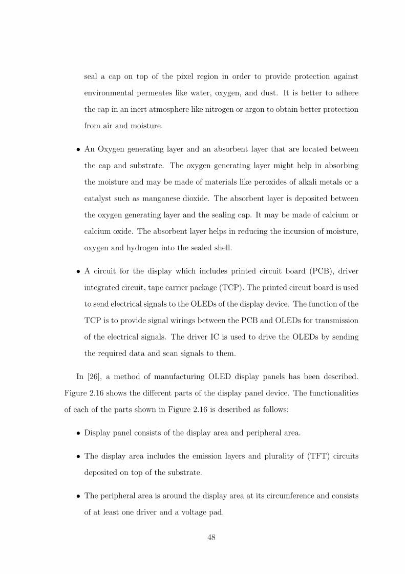
seal a cap on top of the pixel region in order to provide protection against
environmental permeates like water, oxygen, and dust. It is better to adhere
the cap in an inert atmosphere like nitrogen or argon to obtain better protection
from air and moisture.
• An Oxygen generating layer and an absorbent layer that are located between
the cap and substrate. The oxygen generating layer might help in absorbing
the moisture and may be made of materials like peroxides of alkali metals or a
catalyst such as manganese dioxide. The absorbent layer is deposited between
the oxygen generating layer and the sealing cap. It may be made of calcium or
calcium oxide. The absorbent layer helps in reducing the incursion of moisture,
oxygen and hydrogen into the sealed shell.
• A circuit for the display which includes printed circuit board (PCB), driver
integrated circuit, tape carrier package (TCP). The printed circuit board is used
to send electrical signals to the OLEDs of the display device. The function of the
TCP is to provide signal wirings between the PCB and OLEDs for transmission
of the electrical signals. The driver IC is used to drive the OLEDs by sending
the required data and scan signals to them.
In [26], a method of manufacturing OLED display panels has been described.
Figure 2.16 shows the different parts of the display panel device. The functionalities
of each of the parts shown in Figure 2.16 is described as follows:
• Display panel consists of the display area and peripheral area.
• The display area includes the emission layers and plurality of (TFT) circuits
deposited on top of the substrate.
• The peripheral area is around the display area at its circumference and consists
of at least one driver and a voltage pad.
48
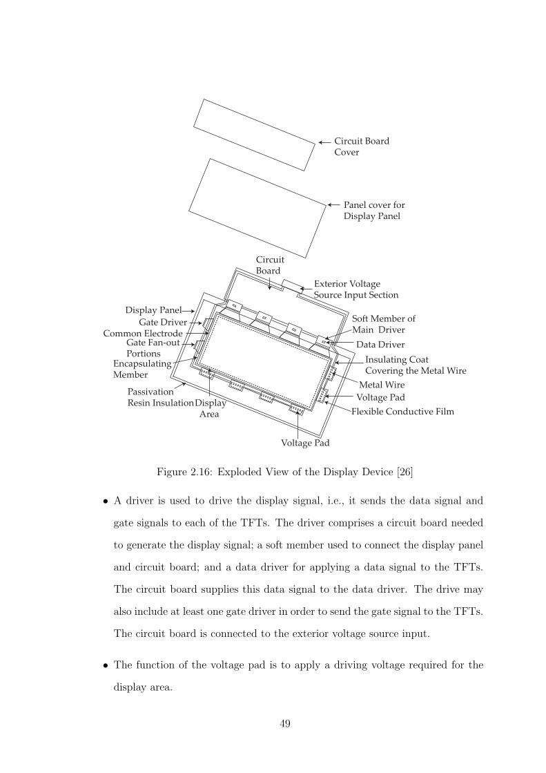
Data Driver
So Member of Main Driver
Exterior Voltage Source Input Section
Metal Wire
Voltage Pad
Voltage Pad
Encapsulating Member
Display Panel
Panel cover for Display Panel
Circuit Board Cover
Circuit Board
Common ElectrodeGate Driver
Display Area
Insulating Coat Covering the Metal Wire
Gate Fan-out Portions
Passivation Resin Insulation
Flexible Conductive Film
Figure 2.16: Exploded View of the Display Device [26]
• A driver is used to drive the display signal, i.e., it sends the data signal and
gate signals to each of the TFTs. The driver comprises a circuit board needed
to generate the display signal; a soft member used to connect the display panel
and circuit board; and a data driver for applying a data signal to the TFTs.
The circuit board supplies this data signal to the data driver. The drive may
also include at least one gate driver in order to send the gate signal to the TFTs.
The circuit board is connected to the exterior voltage source input.
• The function of the voltage pad is to apply a driving voltage required for the
display area.
49
• The necessary driving voltage and common voltage to the voltage pad is pro-
vided by an outer voltage source input section which are connected to each
other using a metal wire. The metal wire is fixed to the voltage pad with the
help of a conductive fixing member.
• In the peripheral region of the display panel, the driving voltage pads are con-
nected to driving voltage lines while the common electrode is electrically con-
nected to common voltage pads. In Figure 2.16, there are many driving voltage
pads at intervals in the peripheral area. The function of each of them is to
apply a predetermined level of driving voltage to the driving voltage line. This
voltage is sent to the driving voltage line through a metal wire of the driving
voltage cable. The voltage required by the driving voltage pad is supplied by the
exterior voltage source input section. These voltage pads are formed opposite
to the data drivers with the display area in between them.
• The peripheral region also consists of many common voltage pads which are
placed at intervals opposite to the gate drivers with the display area in between
them. The common voltage pad applies a predetermined level of common volt-
age to the common electrode via metal wire of common voltage cable. This
voltage is supplied from an exterior voltage input section to the common volt-
age pad.
• The main drivers required for generating the data and the gate signals are also
placed in the peripheral area opposite to the region where the driving voltage
pads are located.
• A substrate for encapsulation of the display panel is provided at the front side
of the panel. Encapsulation is necessary to prevent the moisture and oxygen
from entering the emission layers causing it to degrade.
50
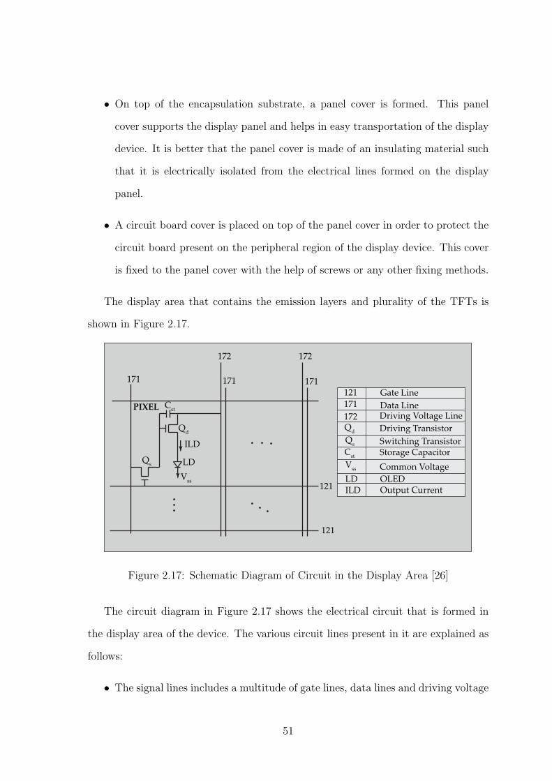
• On top of the encapsulation substrate, a panel cover is formed. This panel
cover supports the display panel and helps in easy transportation of the display
device. It is better that the panel cover is made of an insulating material such
that it is electrically isolated from the electrical lines formed on the display
panel.
• A circuit board cover is placed on top of the panel cover in order to protect the
circuit board present on the peripheral region of the display device. This cover
is fixed to the panel cover with the help of screws or any other fixing methods.
The display area that contains the emission layers and plurality of the TFTs is
shown in Figure 2.17.
PIXEL
121
121
171 171171
172172
Qs
Vss
LD
ILD
Qd
Cst
Driving Voltage LineData Line
Storage Capacitor
Driving Transistor
OLED
Switching Transistor
Output Current
Common Voltage
171
172
121 Gate Line
Qd
Qs
Cst
Vss
LDILD
Figure 2.17: Schematic Diagram of Circuit in the Display Area [26]
The circuit diagram in Figure 2.17 shows the electrical circuit that is formed in
the display area of the device. The various circuit lines present in it are explained as
follows:
• The signal lines includes a multitude of gate lines, data lines and driving voltage
51
lines. The gate lines are used to send gate signals, data lines are used for sending
data signals while the driving voltage lines are used for sending a driving voltage.
• It can be seen that gate lines are considerably in the row direction and are
mostly parallel to each other while the data lines and driving voltage lines are
in the column direction and mostly parallel to each other.
• There will be many pixels in the display area of the device, depending on the
application. Each pixel includes various components like switching transistor,
driving transistor, storage capacitor, and an OLED.
• The switching transistor consists of a control terminal which is connected to the
gate line, an output terminal connected to the driving transistor, and an input
terminal connected to the data line.
• The driving transistor consists of a control terminal, an input terminal, and
an output terminal. The control terminal is connected to the output terminal
of the switching transistor while the input terminal is connected to a driving
voltage line. There is also an output terminal which is being connected to the
OLED.
Table 2.3 shows typical values of layer thickness for an OLED material [27].
2.2 Solar Cells
2.2.1 Introduction
A photovoltaic device consists of semiconducting materials which produces electric
current under the action of light. A device which converts the sun’s energy into
electricity by photovoltaic effect is known as a solar cell; they are also known as
photovoltaic cells. These cells are made of semiconductor materials which absorb
part of the solar energy when light strikes the cell. The energy absorbed in the
52
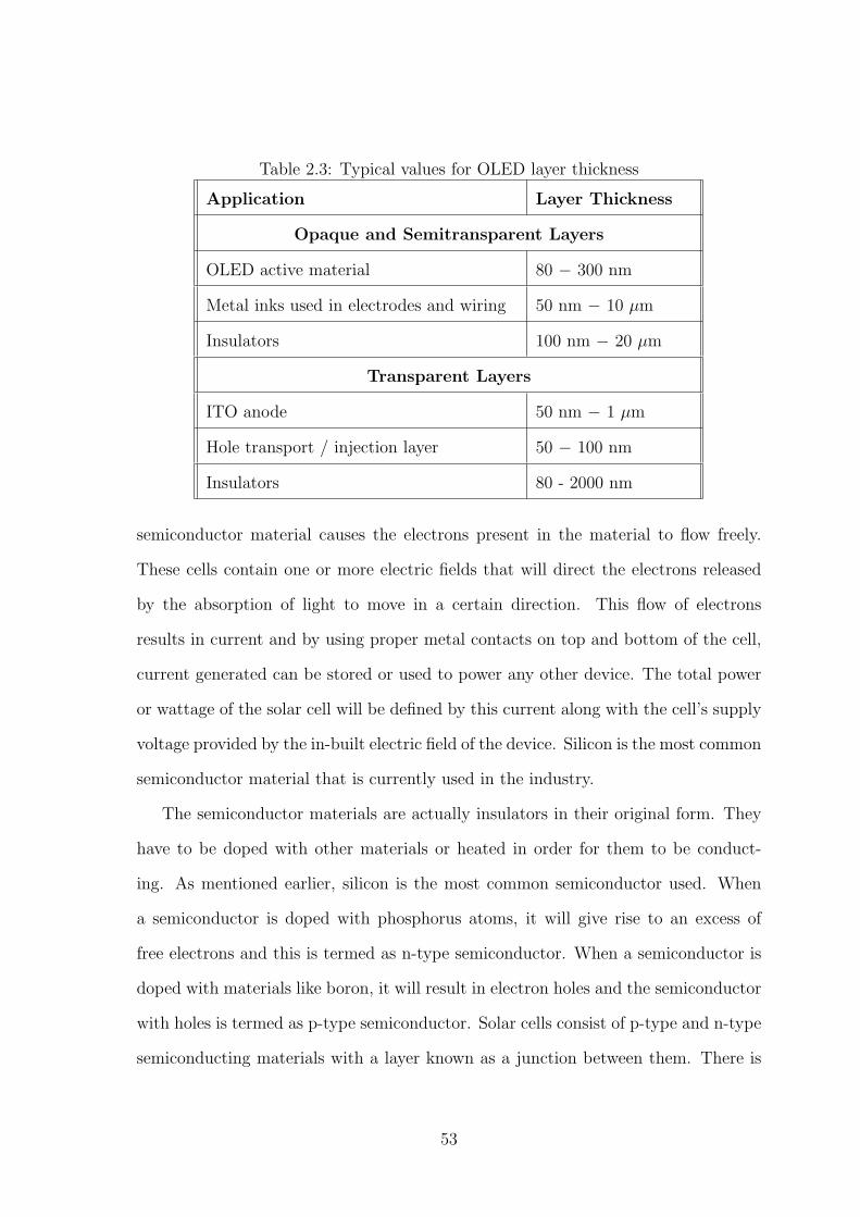
Table 2.3: Typical values for OLED layer thickness
Application Layer Thickness
Opaque and Semitransparent Layers
OLED active material 80 − 300 nm
Metal inks used in electrodes and wiring 50 nm − 10 µm
Insulators 100 nm − 20 µm
Transparent Layers
ITO anode 50 nm − 1 µm
Hole transport / injection layer 50 − 100 nm
Insulators 80 - 2000 nm
semiconductor material causes the electrons present in the material to flow freely.
These cells contain one or more electric fields that will direct the electrons released
by the absorption of light to move in a certain direction. This flow of electrons
results in current and by using proper metal contacts on top and bottom of the cell,
current generated can be stored or used to power any other device. The total power
or wattage of the solar cell will be defined by this current along with the cell’s supply
voltage provided by the in-built electric field of the device. Silicon is the most common
semiconductor material that is currently used in the industry.
The semiconductor materials are actually insulators in their original form. They
have to be doped with other materials or heated in order for them to be conduct-
ing. As mentioned earlier, silicon is the most common semiconductor used. When
a semiconductor is doped with phosphorus atoms, it will give rise to an excess of
free electrons and this is termed as n-type semiconductor. When a semiconductor is
doped with materials like boron, it will result in electron holes and the semiconductor
with holes is termed as p-type semiconductor. Solar cells consist of p-type and n-type
semiconducting materials with a layer known as a junction between them. There is
53
small amount of electron flow from the n-type to p-type material across the junction
even in the absence of light. This will result in a small voltage across the cell. When
light falls on the cell, large amount of electrons will flow from the n-type to p-type
material across the junction which will result in a large amount of current in the
device. This current can be utilized to power other electrical devices.
2.2.2 Flexible Solar Cells
Polymer solar cells are flexible solar cells which are made of very thin active layers,
and these layers can be solution printed at low processing temperature. Similar to
flexible OLEDs, the active materials along with the electrodes in polymer solar cells
are deposited on top of the plastic substrate. Thus, the manufacturing of polymer
solar cells can be achieved by RTR methods. In [28], a solar cell manufactured using
a RTR method is described. In order for the light to be passed to the active layer
of the solar cell, one of the electrodes should be transparent. Presently, ITO is used
as the anode material as it is transparent and can be deposited on flexible plastic
substrates like PET foil along with having the properties desired for being the anode
material. As the sheet resistance of ITO material is high, it can be patterned so
that smaller cells can be connected in series. This would reduce the ohmic loss and
improves the efficiency of the device. In [28], silver material is used for the cathode
layer, zinc oxide is used as an electron transport layer and PEDOT:PSS is used as
the hole conducting layer. In [28], active layer is made of an ink formed by dissolving
P3HT and PCMB ink in a certain ratio in 1,2-dichlorobenzene at around 120o C
temperature. The active layer along with the ZnO and PEDOT layer were slot die
coated onto the ITO-PET substrate. On top of the PEDOT layer, silver cathode layer
is RTR screen printed. The entire device is encapsulated with a flexible barrier layer
using an adhesive. The manufacturing procedure used in [28] is explained below.
Techniques such as slot die coating and screen printing are used to print layers in
54
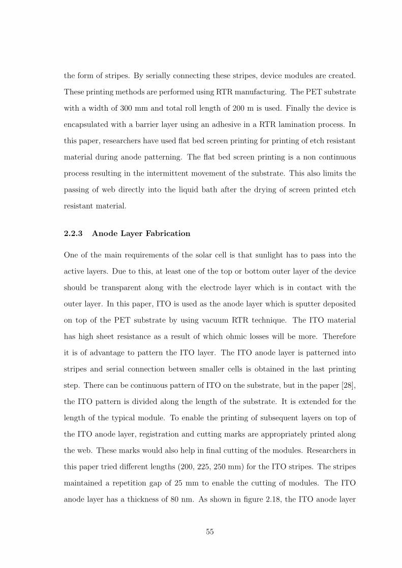
the form of stripes. By serially connecting these stripes, device modules are created.
These printing methods are performed using RTR manufacturing. The PET substrate
with a width of 300 mm and total roll length of 200 m is used. Finally the device is
encapsulated with a barrier layer using an adhesive in a RTR lamination process. In
this paper, researchers have used flat bed screen printing for printing of etch resistant
material during anode patterning. The flat bed screen printing is a non continuous
process resulting in the intermittent movement of the substrate. This also limits the
passing of web directly into the liquid bath after the drying of screen printed etch
resistant material.
2.2.3 Anode Layer Fabrication
One of the main requirements of the solar cell is that sunlight has to pass into the
active layers. Due to this, at least one of the top or bottom outer layer of the device
should be transparent along with the electrode layer which is in contact with the
outer layer. In this paper, ITO is used as the anode layer which is sputter deposited
on top of the PET substrate by using vacuum RTR technique. The ITO material
has high sheet resistance as a result of which ohmic losses will be more. Therefore
it is of advantage to pattern the ITO layer. The ITO anode layer is patterned into
stripes and serial connection between smaller cells is obtained in the last printing
step. There can be continuous pattern of ITO on the substrate, but in the paper [28],
the ITO pattern is divided along the length of the substrate. It is extended for the
length of the typical module. To enable the printing of subsequent layers on top of
the ITO anode layer, registration and cutting marks are appropriately printed along
the web. These marks would also help in final cutting of the modules. Researchers in
this paper tried different lengths (200, 225, 250 mm) for the ITO stripes. The stripes
maintained a repetition gap of 25 mm to enable the cutting of modules. The ITO
anode layer has a thickness of 80 nm. As shown in figure 2.18, the ITO anode layer
55
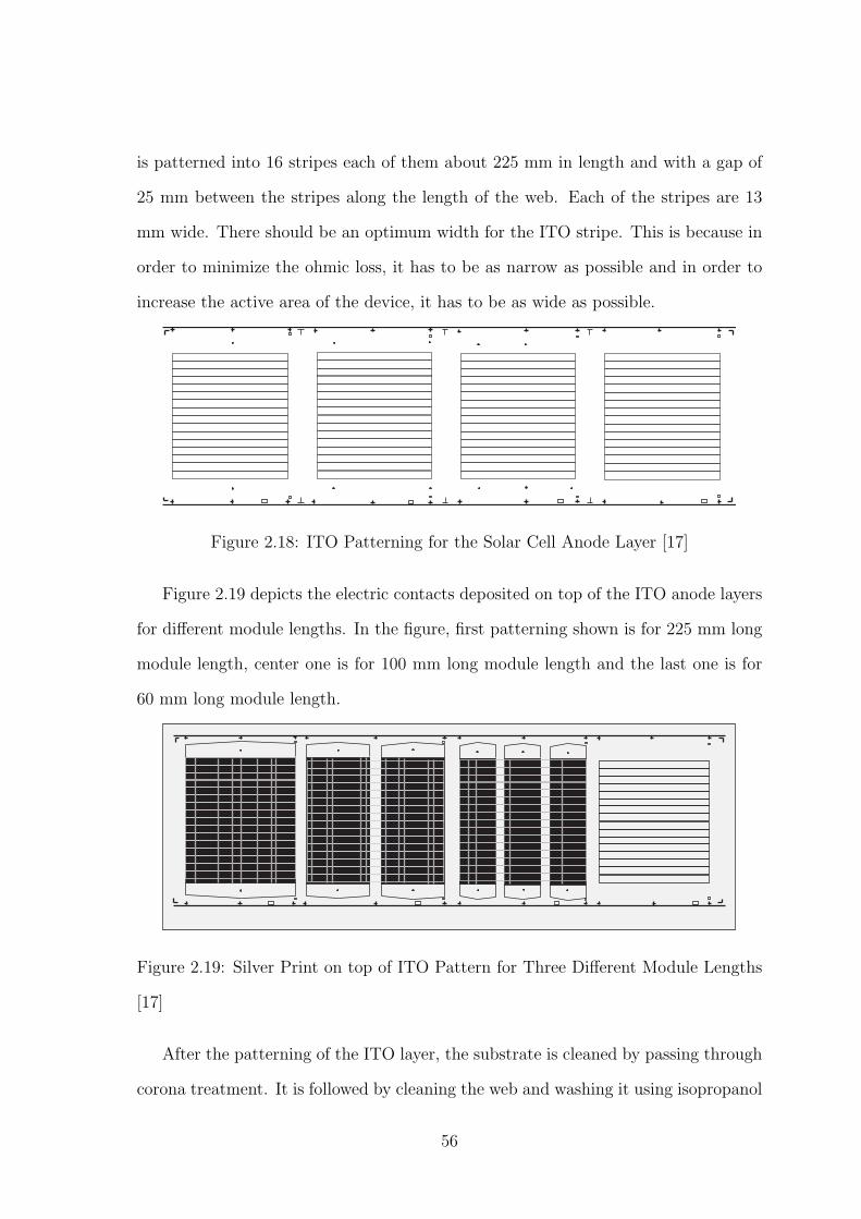
is patterned into 16 stripes each of them about 225 mm in length and with a gap of
25 mm between the stripes along the length of the web. Each of the stripes are 13
mm wide. There should be an optimum width for the ITO stripe. This is because in
order to minimize the ohmic loss, it has to be as narrow as possible and in order to
increase the active area of the device, it has to be as wide as possible.
Figure 2.18: ITO Patterning for the Solar Cell Anode Layer [17]
Figure 2.19 depicts the electric contacts deposited on top of the ITO anode layers
for different module lengths. In the figure, first patterning shown is for 225 mm long
module length, center one is for 100 mm long module length and the last one is for
60 mm long module length.
Figure 2.19: Silver Print on top of ITO Pattern for Three Different Module Lengths
[17]
After the patterning of the ITO layer, the substrate is cleaned by passing through
corona treatment. It is followed by cleaning the web and washing it using isopropanol
56
and then drying it at 140o C. The ITO layer is patterned using a flat bed screen
printing technique. The etch resistant material which is UV curable is screen printed
on top of the raw PET-ITO layer on parts of the substrate where ITO anode is
required. After screen printing, etch resistant material is cured using UV drying
method. A web speed of 3.3 m/min is used for screen printing of etch resistant
material and UV drying method. It is a non-continuous process, as flat bed screen
printing is used. The unprotected areas of the ITO anode layer is then washed away
by passing it through an etching bath which is followed by stripping of the etch
resistant material using a stripping bath. The substrate is then dried at around 140o
C. A web speed of 3 m/min is used for etching, stripping and drying of the substrate.
During the screen printing of etch resistant material, a hole is punched along the
substrate to enable registration during the printing of cathode layer.
2.2.4 Fabrication of active layers
The ZnO solution is slot die coated on top of anode substrate with a speed of about
2 m/min. The thickness of the dry layer obtained is 23 nm. The active layer is also
slot die coated on top of ZnO layer at a speed of 1.4 m/min to obtain a dry layer
thickness of 127 nm. It is then followed by slot die coating of PEDOT:PSS layer
on top of it with a thickness of 20 µm. It is coated at a speed of 0.3 m/min. The
slow speed employed in slot die coating of PEDOT:PSS layer is due to slow drying of
PEDOT:PSS material. A drying length of 1 m and a drying temperature of 140o C
are used for drying these layers.
2.2.5 Fabrication of cathode layer
The cathode layer is screen printed using a RTR screen printer on a flat bed RTR
screen printing machine. The position of cathode pattern on the substrate is in
reference with the hole punched during screen printing of the etch resistant material
57
for the anode layer. In order to print the motif on the substrate, the position is
determined by the registration marks printed during screen printing of the cathode
layer. Based on these registration marks, the substrate is moved to the vacuum table
for printing where it is fixed and printed with the motif. It is then passed through
drying oven at a temperature of 130o C and for a drying length of 120 cm. The web
speed is maintained at 1 m/min.
2.2.6 Lamination of the barrier layer
This is the last step in the fabrication of a solar cell. At first, barrier foil with a
thickness of about 55 µm is coated with an adhesive. The barrier foil has a width
of 305 mm and the adhesive is lined on the foil for a width of 298 mm. The foil
with adhesive is then cut into 250 mm width in order to laminate on the active areas
such that the silver bus bars are exposed for electrical connection. The barrier foil
with the adhesive is laminated on both the sides of the device in order to protect it
from moisture and oxygen. The side with the active layer is laminated first. After
testing of the roll, solar cell sheets are cut using a knife which is triggered when the
registration mark is reached. A camera is employed which recognizes the registration
mark on the substrate that was printed during screen printing and then sends the
signal. Based on this signal, movement of the substrate is stopped and the module is
cut with the knife. These modules are passed over the belt which are then collected
and packed. The length of the ITO stripe does not affect the performance of the
device as the current flow is across the stripes and not along them.
Figure 2.20 shows the entire structure of solar cell module. It can be clearly seen
from the figure the manner in which electrical connection is made with anode and
cathode layers.
In [30], development of a flexible solar cell in RTR form that can be used to charge
a polymer lithium ion battery through a blocking diode is described. These solar cell
58
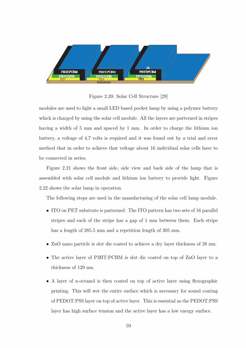
P3HT:PCBM P3HT:PCBMP3HT:PCBM
Al Al Al
PEDOT:PSS PEDOT:PSS PEDOT:PSSITO ITOITO
Substrate
Figure 2.20: Solar Cell Structure [29]
modules are used to light a small LED based pocket lamp by using a polymer battery
which is charged by using the solar cell module. All the layers are patterned in stripes
having a width of 5 mm and spaced by 1 mm. In order to charge the lithium ion
battery, a voltage of 4.7 volts is required and it was found out by a trial and error
method that in order to achieve that voltage about 16 individual solar cells have to
be connected in series.
Figure 2.21 shows the front side, side view and back side of the lamp that is
assembled with solar cell module and lithium ion battery to provide light. Figure
2.22 shows the solar lamp in operation.
The following steps are used in the manufacturing of the solar cell lamp module.
• ITO on PET substrate is patterned. The ITO pattern has two sets of 16 parallel
stripes and each of the stripe has a gap of 1 mm between them. Each stripe
has a length of 285.5 mm and a repetition length of 305 mm.
• ZnO nano particle is slot die coated to achieve a dry layer thickness of 28 nm.
• The active layer of P3HT:PCBM is slot die coated on top of ZnO layer to a
thickness of 129 nm.
• A layer of n-octanol is then coated on top of active layer using flexographic
printing. This will wet the entire surface which is necessary for sound coating
of PEDOT:PSS layer on top of active layer. This is essential as the PEDOT:PSS
layer has high surface tension and the active layer has a low energy surface.
59
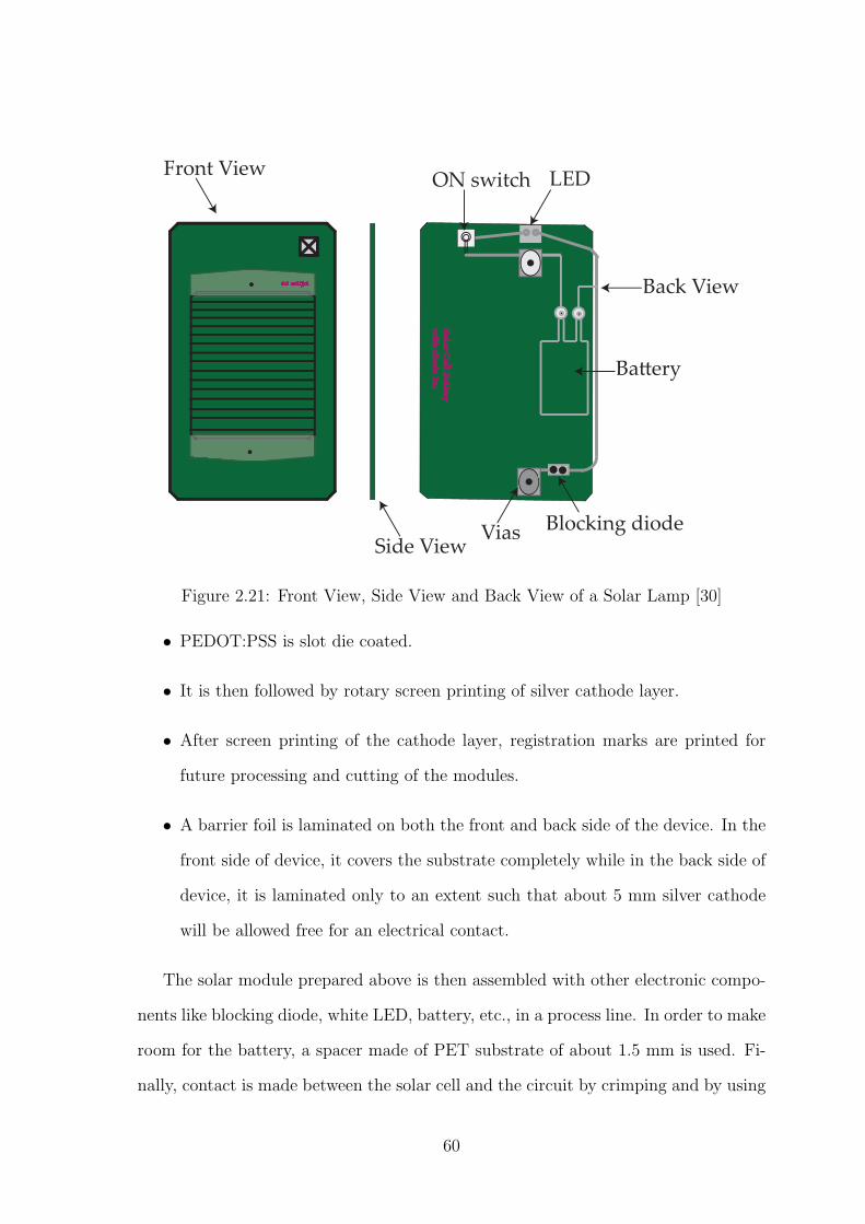
LED
Baery
Blocking diodeVias
ON switch
Side View
Back View
Front View
Figure 2.21: Front View, Side View and Back View of a Solar Lamp [30]
• PEDOT:PSS is slot die coated.
• It is then followed by rotary screen printing of silver cathode layer.
• After screen printing of the cathode layer, registration marks are printed for
future processing and cutting of the modules.
• A barrier foil is laminated on both the front and back side of the device. In the
front side of device, it covers the substrate completely while in the back side of
device, it is laminated only to an extent such that about 5 mm silver cathode
will be allowed free for an electrical contact.
The solar module prepared above is then assembled with other electronic compo-
nents like blocking diode, white LED, battery, etc., in a process line. In order to make
room for the battery, a spacer made of PET substrate of about 1.5 mm is used. Fi-
nally, contact is made between the solar cell and the circuit by crimping and by using
60
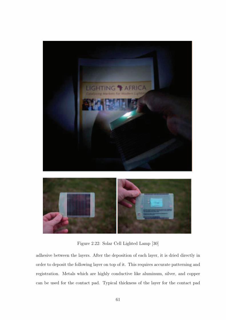
Figure 2.22: Solar Cell Lighted Lamp [30]
adhesive between the layers. After the deposition of each layer, it is dried directly in
order to deposit the following layer on top of it. This requires accurate patterning and
registration. Metals which are highly conductive like aluminum, silver, and copper
can be used for the contact pad. Typical thickness of the layer for the contact pad
61
is about 1−10 µm which will result in efficient conductivity. The contact pad and
bus bars need to be aligned with the electrodes which necessitates the requirement
of resolution and registration. Due to high metal content and viscosity of ink, rotary
screen printing would be the method suitable for deposition of the ink for the contact
pad layer.
An electron transport layer is often preferred between the cathode and active layer
to prevent their interfacial mixing. It is usually made of thin organic material. They
also help in charge transport and defending the photoactive layer from oxidation. The
electron transport layer is typically made of materials like LiF, Ca, Li, ZnO, TiOx,
etc., and some of them are even printable. When they are used for ETL, they are
often dissolved into polar solvents which will assist in wetting and spreading of the
cathode ink and prevent breaking up of the active layer. This layer must be very thin
as the thicker layers can increase the resistance which in turn decrease the efficiency
of the cell. This requires ink to have low viscosity and a printing process such as
gravure printing would be the method suited for deposition.
The transparent barrier layers are usually made of a single layer of oxides or
nitrides. Sometimes they are also made of multiple layers of organic and inorganic
materials. The barrier layer that is laminated is usually made of plastic film coated
with metal or barrier materials.
The transparency of the substrate should be over 90 percent in order to obtain
efficient absorption of the solar light into the active layers of the cell. The photoactive
layers are typically made of low viscosity inks as they have very poor solubility to
solvents. The adhesive layer is printed over the cathode and wiring, after which a
barrier foil is laminated onto it.
Table 2.2.6 show various requirements of each layer of a solar cell device [27].
Figure 2.23 depicts the assembly of a solar cell with the corresponding electrical
circuitry. In addition to the encapsulation of the barrier layers, contact pads must be
62
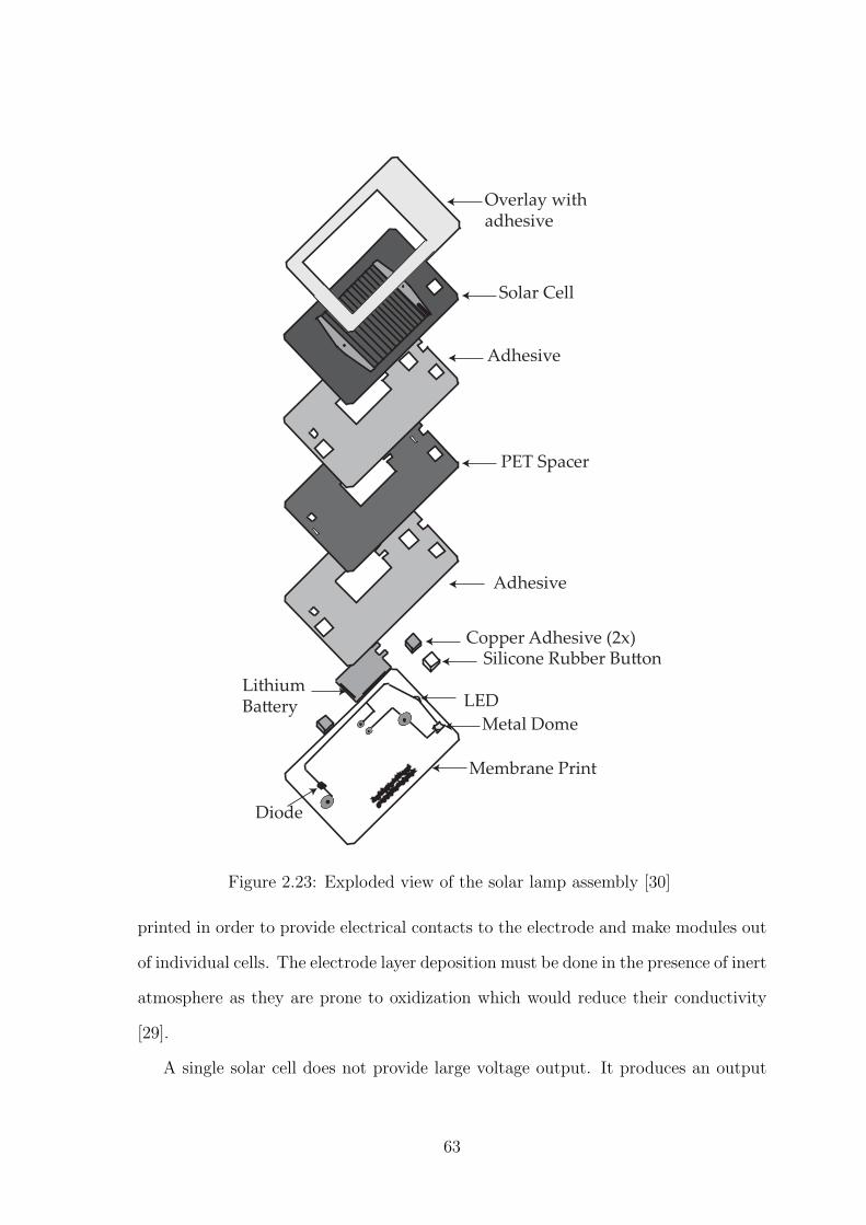
dsgfs
dggfg fs
ddfgggf
gsfgfg
fgfd
gdfgfg
dfgk
Overlay with adhesive
Solar Cell
Adhesive
PET Spacer
Adhesive
Copper Adhesive (2x)Silicone Rubber Buon
LithiumBaery LED
Metal Dome
Membrane Print
Diode
Figure 2.23: Exploded view of the solar lamp assembly [30]
printed in order to provide electrical contacts to the electrode and make modules out
of individual cells. The electrode layer deposition must be done in the presence of inert
atmosphere as they are prone to oxidization which would reduce their conductivity
[29].
A single solar cell does not provide large voltage output. It produces an output
63
voltage of about 0.5 V [29]. Thus, many solar cells have to be connected in series in
order to obtain higher output voltages. As shown in the figure 2.20, the anode of the
first cell is connected to the cathode of the next cell to form a series connection. As
the output current is directly proportional to the active area of the device, the active
area of the device has to be increased to obtain higher electrical power.
The parallel connection of solar cells provides a reliable connection compared to
the series connection. This is because failure of a single solar cell does not affect the
functioning of an entire module. After RTR manufacturing of solar cells or modules,
these sheets must be converted. These solar cells or modules in web form are converted
into desired applications by cutting and slitting. For a solar cell to function properly
for 10,000 hours, it is estimated to have a WVTR value of 10−6 g/m2/day and OTR
value of 10−3 cm3/m2/day. The HIL layer can be printed on top of the patterned
anode layer as a solid patch to avoid the necessity of strict resolution and register
requirements.
64
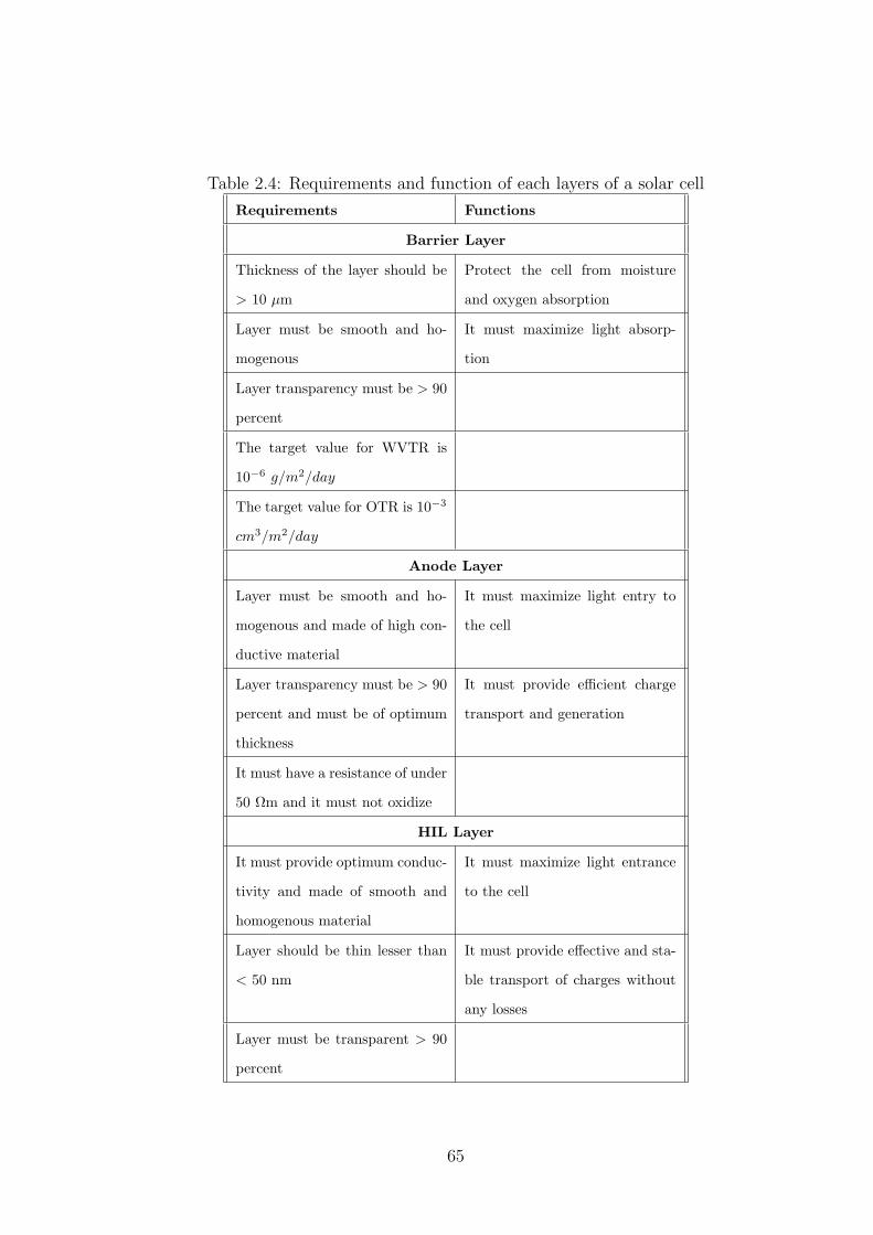
Table 2.4: Requirements and function of each layers of a solar cell
Requirements Functions
Barrier Layer
Thickness of the layer should be
> 10 µm
Protect the cell from moisture
and oxygen absorption
Layer must be smooth and ho-
mogenous
It must maximize light absorp-
tion
Layer transparency must be > 90
percent
The target value for WVTR is
10−6 g/m2/day
The target value for OTR is 10−3
cm3/m2/day
Anode Layer
Layer must be smooth and ho-
mogenous and made of high con-
ductive material
It must maximize light entry to
the cell
Layer transparency must be > 90
percent and must be of optimum
thickness
It must provide efficient charge
transport and generation
It must have a resistance of under
50 Ωm and it must not oxidize
HIL Layer
It must provide optimum conduc-
tivity and made of smooth and
homogenous material
It must maximize light entrance
to the cell
Layer should be thin lesser than
< 50 nm
It must provide effective and sta-
ble transport of charges without
any losses
Layer must be transparent > 90
percent
65
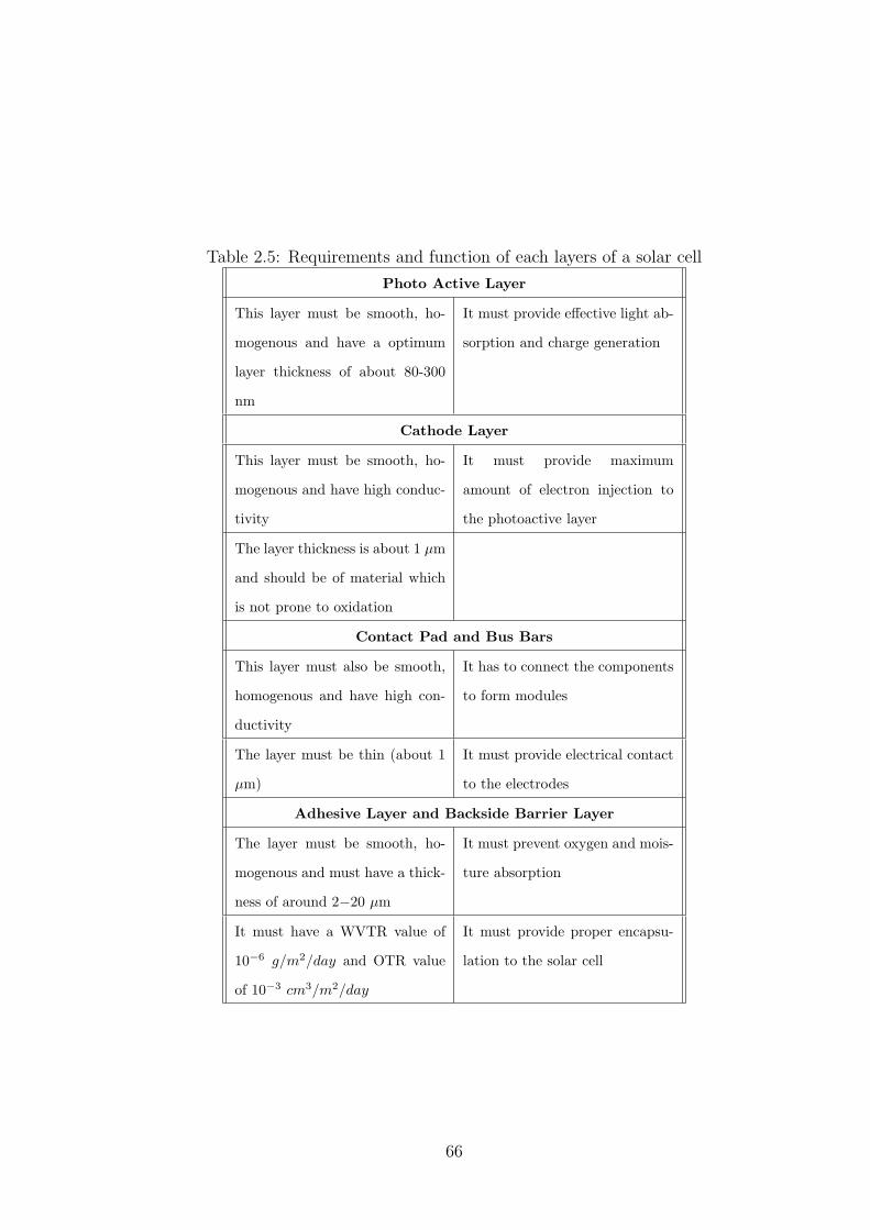
Table 2.5: Requirements and function of each layers of a solar cell
Photo Active Layer
This layer must be smooth, ho-
mogenous and have a optimum
layer thickness of about 80-300
nm
It must provide effective light ab-
sorption and charge generation
Cathode Layer
This layer must be smooth, ho-
mogenous and have high conduc-
tivity
It must provide maximum
amount of electron injection to
the photoactive layer
The layer thickness is about 1 µm
and should be of material which
is not prone to oxidation
Contact Pad and Bus Bars
This layer must also be smooth,
homogenous and have high con-
ductivity
It has to connect the components
to form modules
The layer must be thin (about 1
µm)
It must provide electrical contact
to the electrodes
Adhesive Layer and Backside Barrier Layer
The layer must be smooth, ho-
mogenous and must have a thick-
ness of around 2−20 µm
It must prevent oxygen and mois-
ture absorption
It must have a WVTR value of
10−6 g/m2/day and OTR value
of 10−3 cm3/m2/day
It must provide proper encapsu-
lation to the solar cell
66
CHAPTER 3
Roll to Roll Manufacture of Flexible Electronic Devices
Flexible electronic devices such as flat panel displays and solar cells are not currently
manufactured in rolled form. Although some elements during the manufacturing of
these devices may currently involve roll to roll processing, RTR manufacturing of
the entire production of these devices has not been accomplished yet. Designing
and developing an RTR process line that is capable of producing these devices in
rolled form is expected to significantly improve productivity and reduce the cost of
manufacturing. As a result there is a strong research and development effort towards
achieving this goal in commercial companies, research laboratories, and academic
institutions. Current manufacturing of these devices involves a considerable amount
of batch processing. In order to manufacture the flexible electronics in RTR form,
proper selection of materials along with processing methods which assist in RTR
manufacturing must be used. Materials for the layers of flexible electronic devices
must be chosen such that they can be deposited on the substrate using the techniques
that are compatible with RTR manufacturing. Similarly, process methods and devices
must be selected to be compatible with RTR manufacturing. Understanding of the
various key methods of web handling is key to developing RTR methods and design
of RTR machines for manufacture of flexible electronic devices.
Although manufacture of many flexible electronic devices are being envisioned,
the focus in this chapter is on manufacturing of OLEDs, which is expected to be
applicable for flat panel displays and flat panel lighting. In first section of this chapter,
materials that are suitable for RTR manufacturing of flexible OLED devices and
67
their properties are discussed. One such material is indium tin oxide (ITO), which
is used in many flexible devices such as LCDs, OLEDs, plasma displays, and solar
cells. The ITO material cannot be solution printed directly on a web substrate;
it is deposited on the surface by different techniques which were described in the
previous chapter. After deposition it is patterned using different techniques. The
currently available patterning techniques are expensive and cannot be performed in a
continuous manner. The flexible electronics industry could benefit a great deal if such
patterning could be successfully performed using solution printing techniques that are
compatible with RTR manufacturing. From the literature it appears that there has
been substantial progress in recent years on developing these solutions in appropriate
composition which will facilitate patterning of the ITO anode on a plastic substrate.
Design of a web line for patterning of ITO anode on a plastic substrate is discussed
in the second section of this chapter. Appropriate patterning of the anode layer is
critical to the working of an entire device. It reduces the overall resistance of the
conducted and helps in obtaining better resolution devices. Various key technologies,
processes and devices are selected for the web line such that ITO patterning can
be performed as continuous process in this web line. The ITO patterned substrate
can be used for manufacturing of flexible electronic devices such as OLEDs, polymer
solar cells, LCDs, etc. The third section of this chapter discusses the design of a web
line that is capalbe of depositing the active layers of OLED lighting devices on an
ITO patterned PET substrate. The web line processing conditions, parameters, and
printing technologies are chosen such that the layers can be deposited in a continuous
manner during transport of the flexible material. Although flexible OLED lighting
devices is the focus for the development of this web line, similar web line designs can
be used for fabrication of other flexible devices also, except that the materials and
process parameters may change.
68
3.1 Solution Printed Flexible OLEDs
Based on a comprehensive and investigative study of available literature, materials
and process that make the different components of flexible OLED lighting devices are
determined and are summarized below. Further discussions are provided in subse-
quent sections when the design of the two web lines are discussed.
• Indium tin oxide (ITO) is used as an anode layer on polyethylene terephthalate
(PET) substrate. The ITO material can be deposited by a sputter deposition
process on PET substrate to obtain the ITO-PET layer. ITO anode may be
patterned depending on the application of the OLED device.
• PEDOT:PSS ink is used for the hole injection layer. This layer is made of
about 40 nm thickness and is gravure printed on top of anode layer on the PET
substrate.
• Poly-dihexylfluorene-alt-benzothiadiazol (PFBT), a yellow color emitting poly-
mer layer is deposited onto the hole injection layer. The thickness of this layer
is about 70 nm and is gravure printed on top of the PEDOT:PSS layer.
• An insulating layer is screen printed on the emissive layer in order to separate it
from the cathode layer and to complement electron transport from the cathode
layer.
• Aluminum is used as the cathode material and is rotary screen printed on top
of the insulating layer. As the printed cathode material is sensitive to air when
in liquid form, it is required to print the cathode layer in the inert atmosphere.
• Silver wiring is then rotary screen printed on top of the aluminium cathode
layer.
69
• Finally, the OLED device is encapsulated with a barrier layer in order to protect
it from moisture and oxygen. This is achieved by laminating the substrate with
a barrier layer using a suitable adhesive.
3.2 Design of a Web Line for Patterning of ITO Anode Layer on PET
Substrate
In this section, design of a web line for patterning of anode material on a PET
substrate is discussed. The ITO deposited PET substrate is unwound from a roll and
passed through the following series of operations to obtain a desired pattern of the
anode on the substrate.
• An etch resistant material is rotary screen printed on the ITO-PET substrate
on the areas where ITO pattern is required.
• It is then passed through an UV curing process where the etch resistant material
is cured.
• The resulting substrate is then passed through an etching bath of aqueous
cupric-chloride (CuCl2) in order to remove the ITO from the unprotected areas
of the substrate.
• The web is then passed thorough a stripping bath of sodium hydroxide in order
to remove the etch resistant material from the substrate, which will result in an
ITO patterned substrate.
• Finally, the web is washed by passing through demineralized water and dried
by passing through a section of hot air.
The following subsections provide detailed discussion of various available technologies
used in the web line for ITO patterning, and the reasons for the selection of some
technologies that are appropriate for RTR processing.
70
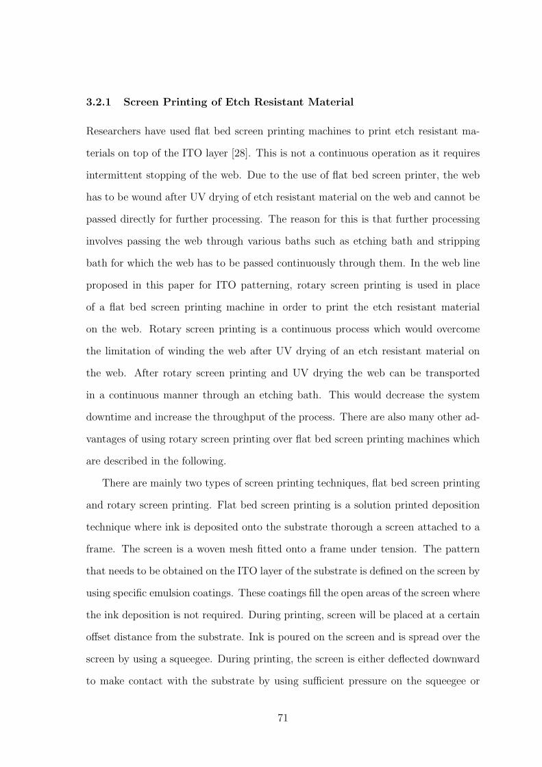
3.2.1 Screen Printing of Etch Resistant Material
Researchers have used flat bed screen printing machines to print etch resistant ma-
terials on top of the ITO layer [28]. This is not a continuous operation as it requires
intermittent stopping of the web. Due to the use of flat bed screen printer, the web
has to be wound after UV drying of etch resistant material on the web and cannot be
passed directly for further processing. The reason for this is that further processing
involves passing the web through various baths such as etching bath and stripping
bath for which the web has to be passed continuously through them. In the web line
proposed in this paper for ITO patterning, rotary screen printing is used in place
of a flat bed screen printing machine in order to print the etch resistant material
on the web. Rotary screen printing is a continuous process which would overcome
the limitation of winding the web after UV drying of an etch resistant material on
the web. After rotary screen printing and UV drying the web can be transported
in a continuous manner through an etching bath. This would decrease the system
downtime and increase the throughput of the process. There are also many other ad-
vantages of using rotary screen printing over flat bed screen printing machines which
are described in the following.
There are mainly two types of screen printing techniques, flat bed screen printing
and rotary screen printing. Flat bed screen printing is a solution printed deposition
technique where ink is deposited onto the substrate thorough a screen attached to a
frame. The screen is a woven mesh fitted onto a frame under tension. The pattern
that needs to be obtained on the ITO layer of the substrate is defined on the screen by
using specific emulsion coatings. These coatings fill the open areas of the screen where
the ink deposition is not required. During printing, screen will be placed at a certain
offset distance from the substrate. Ink is poured on the screen and is spread over the
screen by using a squeegee. During printing, the screen is either deflected downward
to make contact with the substrate by using sufficient pressure on the squeegee or
71
ink is just passed onto the substrate through the screen without the screen making
contact with the substrate. As the squeegee passes a given point on the screen,
screen fabric tension moves the screen back leaving the ink on the substrate. The wet
thickness of the film that can be obtained on the substrate thorough this process can
be controlled by the volume defined between the threads of the screen and thickness
of the emulsion coating. Usually rectangular screens are used for printing, but rotary
screens in cylindrical shape are used in a rotary screen printer. The selection of the
screen type depends on various factors such as viscosity of the ink and accuracy of
pattern required, etc. Mesh size of a screen is measured by the number of threads
of mesh per square inch. Mesh sizes selected for a particular screen depend on the
application. It defines the detail of the image that needs to be printed and also the
thickness of ink. As the mesh count increases, the threads and holes in the screen
are finer. An image with a very high detail cannot be printed by using a lower mesh
screen and also if the ink is thinner, it will easily pass through the screen holes which
may result in a blurry image. Figure 3.1 shows an illustration of the flat bed screen
printing process; please note that all the figures and tables for this chapter are shown
at the end of the chapter. Currently available screen printing machines are capable
of producing a screen print of 10-20 micron lines and spaces. Some of the key terms
associated with screen printing are given in the following.
• Stroke: The stroke is defined as the one complete movement of the squeegee
across the screen. Generally, there are two types of strokes involved in screen
printing, namely, flood stroke and print stroke. Both these strokes have different
purposes and are defined below.
1. Flood Stroke: It is the first stroke and it spreads the ink across the screen
and prepares it for the execution of the print stroke. The mesh opening
will be filled with ink during this stroke. The squeegee cannot be moved
72
with a high pressure during this stroke when compared to the print stroke
but sufficient pressure is applied to spread the ink across the screen.
2. Print Stroke: During this stroke the ink is forced through the mesh open-
ings by the squeegee moving across the screen. A single movement of the
squeegee across the screen is considered as one stroke. During this stroke,
three important actions are performed. The mesh is brought down onto
the surface of the substrate, then the squeegee moves across the substrate
forcing the ink through it, and lastly, excess ink remaining on the screen
will be carried away to the far end of the screen. When the squeegee ap-
plies pressure on the screen, it actually adds extra tension into the screen.
Initially, the screen will be at some tension due to stretching of the screen
as it is fitted into the frame, which is referred to as static tension. The
additional tension caused by the squeegee pressure is called the dynamic
tension. The mesh tries to resist this dynamic tension and tries to re-
turn to its original position which is an important factor in the working
of screen printing. During printing, only the line of mesh underneath the
squeegee comes in contact with the substrate at any point of time and
as soon as the squeegee blade passes that point, the mesh recoils back
to its original position due to its static tension. During the second part,
squeegee forces the ink through the mesh by applying a force and finally
as it moves through the screen, it also cuts any extra ink present above
the mesh thread.
• Double Stroking: Sometimes, if the print is not good with the first pass, the
squeegee is passed over the screen twice during the print stroke which is termed
as double stroking. It does not necessarily improve the quality of the print but
it will produce a thicker print.
73
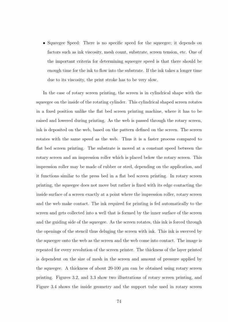
• Squeegee Speed: There is no specific speed for the squeegee; it depends on
factors such as ink viscosity, mesh count, substrate, screen tension, etc. One of
the important criteria for determining squeegee speed is that there should be
enough time for the ink to flow into the substrate. If the ink takes a longer time
due to its viscosity, the print stroke has to be very slow.
In the case of rotary screen printing, the screen is in cylindrical shape with the
squeegee on the inside of the rotating cylinder. This cylindrical shaped screen rotates
in a fixed position unlike the flat bed screen printing machine, where it has to be
raised and lowered during printing. As the web is passed through the rotary screen,
ink is deposited on the web, based on the pattern defined on the screen. The screen
rotates with the same speed as the web. Thus it is a faster process compared to
flat bed screen printing. The substrate is moved at a constant speed between the
rotary screen and an impression roller which is placed below the rotary screen. This
impression roller may be made of rubber or steel, depending on the application, and
it functions similar to the press bed in a flat bed screen printing. In rotary screen
printing, the squeegee does not move but rather is fixed with its edge contacting the
inside surface of a screen exactly at a point where the impression roller, rotary screen
and the web make contact. The ink required for printing is fed automatically to the
screen and gets collected into a well that is formed by the inner surface of the screen
and the guiding side of the squeegee. As the screen rotates, this ink is forced through
the openings of the stencil thus deluging the screen with ink. This ink is swerved by
the squeegee onto the web as the screen and the web come into contact. The image is
repeated for every revolution of the screen printer. The thickness of the layer printed
is dependent on the size of mesh in the screen and amount of pressure applied by
the squeegee. A thickness of about 20-100 µm can be obtained using rotary screen
printing. Figures 3.2, and 3.3 show two illustrations of rotary screen printing, and
Figure 3.4 shows the inside geometry and the support tube used in rotary screen
74
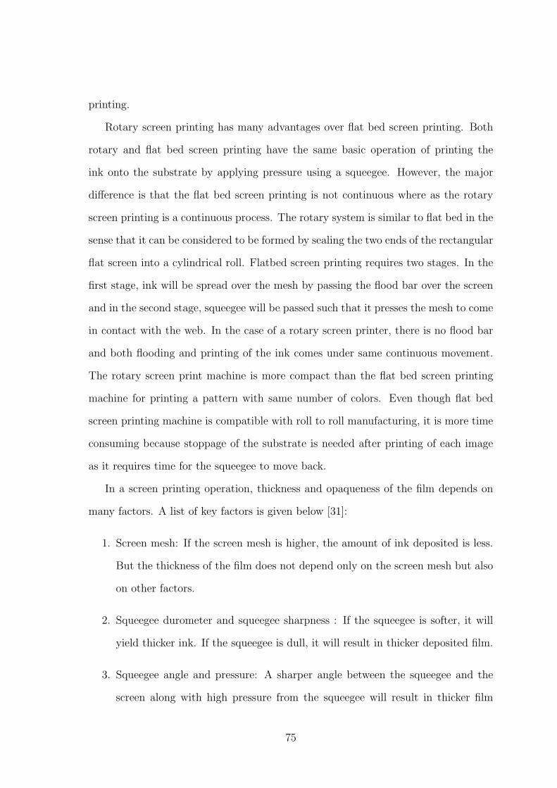
printing.
Rotary screen printing has many advantages over flat bed screen printing. Both
rotary and flat bed screen printing have the same basic operation of printing the
ink onto the substrate by applying pressure using a squeegee. However, the major
difference is that the flat bed screen printing is not continuous where as the rotary
screen printing is a continuous process. The rotary system is similar to flat bed in the
sense that it can be considered to be formed by sealing the two ends of the rectangular
flat screen into a cylindrical roll. Flatbed screen printing requires two stages. In the
first stage, ink will be spread over the mesh by passing the flood bar over the screen
and in the second stage, squeegee will be passed such that it presses the mesh to come
in contact with the web. In the case of a rotary screen printer, there is no flood bar
and both flooding and printing of the ink comes under same continuous movement.
The rotary screen print machine is more compact than the flat bed screen printing
machine for printing a pattern with same number of colors. Even though flat bed
screen printing machine is compatible with roll to roll manufacturing, it is more time
consuming because stoppage of the substrate is needed after printing of each image
as it requires time for the squeegee to move back.
In a screen printing operation, thickness and opaqueness of the film depends on
many factors. A list of key factors is given below [31]:
1. Screen mesh: If the screen mesh is higher, the amount of ink deposited is less.
But the thickness of the film does not depend only on the screen mesh but also
on other factors.
2. Squeegee durometer and squeegee sharpness : If the squeegee is softer, it will
yield thicker ink. If the squeegee is dull, it will result in thicker deposited film.
3. Squeegee angle and pressure: A sharper angle between the squeegee and the
screen along with high pressure from the squeegee will result in thicker film
75
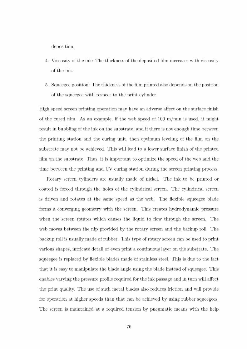
deposition.
4. Viscosity of the ink: The thickness of the deposited film increases with viscosity
of the ink.
5. Squeegee position: The thickness of the film printed also depends on the position
of the squeegee with respect to the print cylinder.
High speed screen printing operation may have an adverse affect on the surface finish
of the cured film. As an example, if the web speed of 100 m/min is used, it might
result in bubbling of the ink on the substrate, and if there is not enough time between
the printing station and the curing unit, then optimum leveling of the film on the
substrate may not be achieved. This will lead to a lower surface finish of the printed
film on the substrate. Thus, it is important to optimize the speed of the web and the
time between the printing and UV curing station during the screen printing process.
Rotary screen cylinders are usually made of nickel. The ink to be printed or
coated is forced through the holes of the cylindrical screen. The cylindrical screen
is driven and rotates at the same speed as the web. The flexible squeegee blade
forms a converging geometry with the screen. This creates hydrodynamic pressure
when the screen rotates which causes the liquid to flow through the screen. The
web moves between the nip provided by the rotary screen and the backup roll. The
backup roll is usually made of rubber. This type of rotary screen can be used to print
various shapes, intricate detail or even print a continuous layer on the substrate. The
squeegee is replaced by flexible blades made of stainless steel. This is due to the fact
that it is easy to manipulate the blade angle using the blade instead of squeegee. This
enables varying the pressure profile required for the ink passage and in turn will affect
the print quality. The use of such metal blades also reduces friction and will provide
for operation at higher speeds than that can be achieved by using rubber squeegees.
The screen is maintained at a required tension by pneumatic means with the help
76
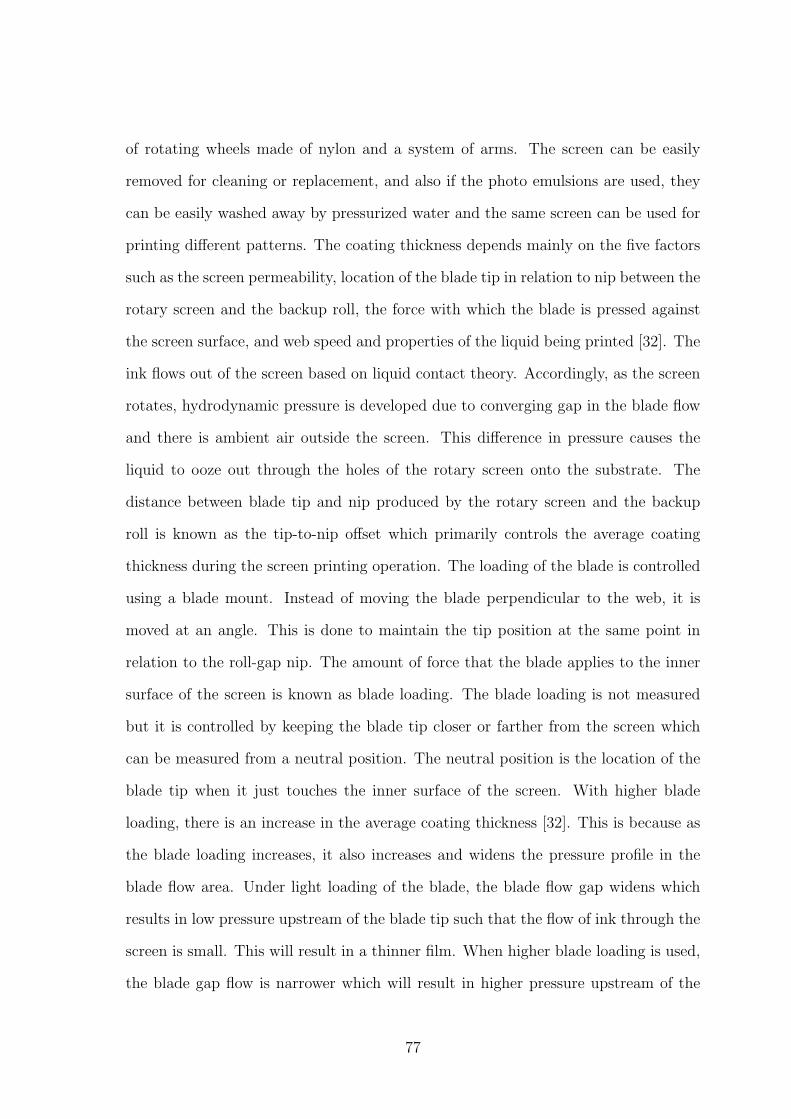
of rotating wheels made of nylon and a system of arms. The screen can be easily
removed for cleaning or replacement, and also if the photo emulsions are used, they
can be easily washed away by pressurized water and the same screen can be used for
printing different patterns. The coating thickness depends mainly on the five factors
such as the screen permeability, location of the blade tip in relation to nip between the
rotary screen and the backup roll, the force with which the blade is pressed against
the screen surface, and web speed and properties of the liquid being printed [32]. The
ink flows out of the screen based on liquid contact theory. Accordingly, as the screen
rotates, hydrodynamic pressure is developed due to converging gap in the blade flow
and there is ambient air outside the screen. This difference in pressure causes the
liquid to ooze out through the holes of the rotary screen onto the substrate. The
distance between blade tip and nip produced by the rotary screen and the backup
roll is known as the tip-to-nip offset which primarily controls the average coating
thickness during the screen printing operation. The loading of the blade is controlled
using a blade mount. Instead of moving the blade perpendicular to the web, it is
moved at an angle. This is done to maintain the tip position at the same point in
relation to the roll-gap nip. The amount of force that the blade applies to the inner
surface of the screen is known as blade loading. The blade loading is not measured
but it is controlled by keeping the blade tip closer or farther from the screen which
can be measured from a neutral position. The neutral position is the location of the
blade tip when it just touches the inner surface of the screen. With higher blade
loading, there is an increase in the average coating thickness [32]. This is because as
the blade loading increases, it also increases and widens the pressure profile in the
blade flow area. Under light loading of the blade, the blade flow gap widens which
results in low pressure upstream of the blade tip such that the flow of ink through the
screen is small. This will result in a thinner film. When higher blade loading is used,
the blade gap flow is narrower which will result in higher pressure upstream of the
77
blade tip such that the flow on ink through the screen is large. This will provide a
thicker film. Rotary screen printing is a robust and reliable method as the thickness
of the layer printed is consistent if the quantities such as squeegee pressure or angle
are not changed during the printing process. Currently, the range of line widths that
can be achieved with rotary screen printing is 50-100 µm. Since this method uses
very little nip pressure, it a safer method to print multilayered structures.
After rotary screen printing of the etch resistant material onto the substrate, it
is passed through an UV drying chamber in order to cure the printed etch resistant
material. The following section describes the UV drying process.
3.2.2 Ultra Violet (UV) curing
Ultra-Violet light is a part of the electromagnetic spectrum with wavelengths between
200-400 nanometers. UV curing is a process where the wet film that is deposited on a
substrate is solidified by exposing high energy radiation. Unlike conventional drying,
UV curing involves a cross-linking reaction along with the evaporation of a solvent.
It also results in superior physical properties than obtained using conventional dry-
ing. UV curing system gives good physical properties and solvent resistance to the
cured film. It is a very fast process of curing and just takes a few seconds to dry
a film. UV spot lamps or UV flood lamps can be used to cure the film depending
on the application. The former one provides a high intensity UV light on a smaller
area whereas the latter one provides moderate intensity UV light over a larger area.
Mercury vapor lamps are the most common source of UV light used for UV curing
processes and produces light either by passing electric current into a quartz contain-
ing mercury or by energizing mercury using microwaves. UV cured films will have
a very smooth finish as a result of very fast curing. In the case of screen printing
with conventional drying inks, the ink may dry on the screen itself which is always
a problem. This happens due to the evaporation of the solvent present in the ink.
78
This requires frequent cleaning of the screen whenever there is a break in the printing
process. In the case of UV curing inks, this problem does not occur and the screen
need not be cleaned every time the press is stopped. Generally, screens are cleaned
once a week when UV cured ink is used for screen printing. Labor is always a key
factor in a printing press. If the conventional inks are used for screen printing, there
are problems involved in racking and stacking of the prints whereas if the ink used
is UV curable, as soon as it exits the curing unit, it can be either stacked up imme-
diately or can be used for further processing without any waiting time. Thus, both
labor and time is reduced in the case of screen printing operations with UV curing
inks. Since, the UV curing system consumes less space, space savings can also be
achieved by using UV curing system instead of conventional drying units or ovens.
UV cured films are biodegradable and are environmentally safe. They provide very
high curing speeds and web speeds of up to 100 m/min are possible. It generates less
heat and therefore is suitable for heat sensitive substrates. As the film cures fast,
the turnaround time is greatly increased. It is reported that the capital investment
for UV-curing unit is substantially less compared to conventional drying unit and a
complete installation of a UV curing setup does not involve more than one-half of
that used for a conventional drying unit [31].
The curing speed depends on many factors. It depends not only on the curing unit
but also on the color of the substrate color and the color of ink. If the substrate is
white or light in color, it has the ability to reflect the unabsorbed UV light back onto
the film. Thus the curing speed will be higher for the substrate which is white or light
in color compared to black or dark colored substrate. Also, printing on transparent
films with reflective support will increase the curing speed. It is know that ink cures
faster with UV curing if it is red or yellow in color than black or white colored ink
[31]. This is because of the low transmission of the UV light by pigments present in
the white or black colored ink than the red or yellow ones. The curing speed depends
79
on the following factors of an UV curing unit.
1. Intensity of the UV light: In order to double the curing speed, intensity of the
light has to be increased by four times.
2. Number of UV sources: The curing speed is directly proportional to the number
of UV lamps and the exposure time. As the exposure time is increased, the
curing speed can be increased also. But the web speed is inversely proportional
to the exposure time. Thus, the curing speed, web speed and number of UV
lamps required for curing are interrelated. Lower web speeds for very fast curing
UV inks will result in over curing of the ink which will affect the flexibility of
the film layer, adhesion of coating, etc.
3. Temperature: Very high temperature during curing will cause problems, espe-
cially in the case of substrate made of paper and some of the plastic materials.
These materials undergo change in their dimensional property when they are
subjected to high temperature conditions. It is very crucial to maintain a low
optimum curing temperature when using heat sensitive plastic substrates dur-
ing an UV curing process. The temperature of the substrate can be controlled
by using low powered UV lamps, by increasing the web speed or by using an
UV unit with efficient cooling systems. But in the case of non-heat sensitive
material substrate such as steel, thick plastics, glass etc., a higher tempera-
ture is beneficial. In such cases, higher temperature will increase the adhesion
property and will also increase the curing speed of the ink.
4. Effect of inert atmosphere: During the UV curing process, the oxygen in air
reacts with atoms that causes curing of the ink and thus inhibits the curing
process. So, the presence of inert atmosphere during UV drying will overcome
this problem. Nitrogen is generally used as the gas for maintaining inert atmo-
sphere.
80
The UV curing process reduces air pollution and also reduces solvent vapor gen-
eration as compared to other thermal curing processes. Reducing solvent vapor gen-
eration saves a significant amount of energy. For the web line that is designed in this
thesis, a pulsed UV curing device that cures the material on the substrate at low
temperature is used. UV curing of a material can be done on a substrate using a
pulsed UV curing device at a very low temperature and in a continuous manner. The
process involves passing the substrate after screen printing the UV curable etch resis-
tant material into the UV chamber where it is subjected to a high intensity pulsed UV
light in order to cure the material on the substrate. When conventional UV curing
devices are used, the process of curing is complicated because of high temperature
involved with conventional UV curing devices. The conventional UV curing light
sources such as mercury lamps operate at a high temperature of up to 1000o C. Even
though cooling equipments are associated with conventional light sources, a substan-
tial amount of infrared heat is formed which will heat the substrate. Due to this heat,
the pattern printed on the substrate may be damaged or distorted. It may even melt
if the heat developed is higher. The UV curing device is placed soon after the screen
printing device such that the web is pushed or pulled through the section of coating
and curing by mechanical means without any contact of the pattered material on
the mechanical support after printing until it is cured. Driven pull rollers are placed
before the screen printing device and after the UV curing device such that the web
continuously passes through these processes with a desired tension. Conveyor belts
cannot be used due to the fact that screen printing operation is used for printing the
etch resistant material and screen printing involves the use of impression roller along
with the screen printer [33]. It is desirable to place the UV drying chamber close to
the screen printing machine. This will avoid problems such as unwanted oxidation,
evaporation or maturing of the uncured printed material. It is also better to keep
the distance between the screen printed and UV drying machine within one meter.
81
The temperature is not increased much during this cold curing operation and is typ-
ically not more than 50o C. The pulsed UV curing light is supplied to the substrate
at the ambient temperature or at low temperature. There might be some heating
involved in this process but it is exothermic heat which does not heat the substrate.
Even cold inert gas may be supplied in order to lower the temperature within the
curing chamber. The temperature of cold UV curing process may be between 10-33o
C. Even a temperature lower than the ambient temperature may be obtained during
a cold UV curing operation [33]. Sometimes there might be a striping effect when
passing a web continuously under a UV lamp. Striping effect involves partial cured
and uncured sections of the material which needs to be cured after the web leaves
the UV curing section. In order to avoid striping effect, the pulsed UV source should
at least have a flash frequency of 10 pulses per second (pps). The flash frequency
value of even 100 pps may also be desired. Multiple pulsed UV lamps within the
UV chamber for curing may be also be desirable. Whenever more than one lamp is
used, it is necessary to coordinate the pulsing of the lamps such that faster and better
curing is obtained without any striping effect. The use of a cold UV curing device
will result in better curing of the material on the substrate, as there is not much heat
involved compared to the conventional UV lamps. Moreover, the substrate will not
be subjected to any thermal stresses and also any problems such as discoloration that
occurs due to the scorching of the plastic substrate is eliminated. Unlike conventional
lamps, pulsed UV lamps do not require any warm up period prior to operation. This
saves time and energy, especially when there is a break involved in the process such
as for maintenance or any other operator breaks. With this process, the web may be
transported at speeds between 20 to 90 m/min.
After the curing of etch resistant material, the web is passed through an etch-
ing bath of aqueous Cupric Chloride solution where the unprotected anode material
present on the substrate is etched. The process of etching is described in the section
82
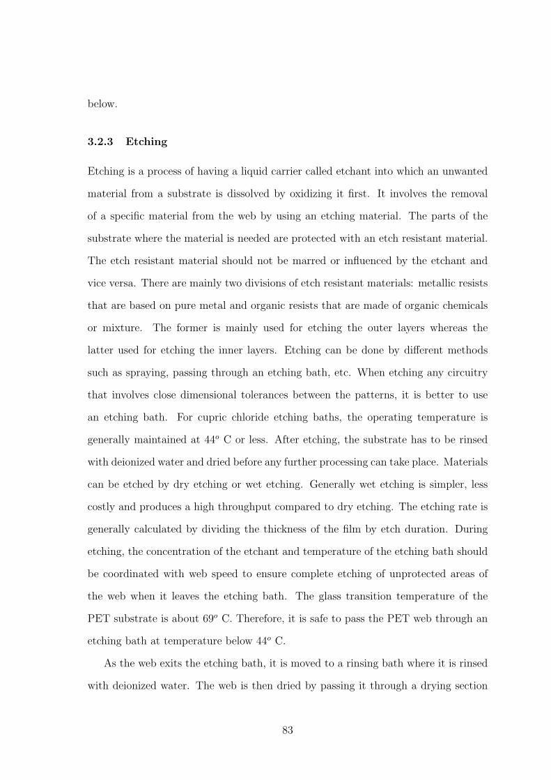
below.
3.2.3 Etching
Etching is a process of having a liquid carrier called etchant into which an unwanted
material from a substrate is dissolved by oxidizing it first. It involves the removal
of a specific material from the web by using an etching material. The parts of the
substrate where the material is needed are protected with an etch resistant material.
The etch resistant material should not be marred or influenced by the etchant and
vice versa. There are mainly two divisions of etch resistant materials: metallic resists
that are based on pure metal and organic resists that are made of organic chemicals
or mixture. The former is mainly used for etching the outer layers whereas the
latter used for etching the inner layers. Etching can be done by different methods
such as spraying, passing through an etching bath, etc. When etching any circuitry
that involves close dimensional tolerances between the patterns, it is better to use
an etching bath. For cupric chloride etching baths, the operating temperature is
generally maintained at 44o C or less. After etching, the substrate has to be rinsed
with deionized water and dried before any further processing can take place. Materials
can be etched by dry etching or wet etching. Generally wet etching is simpler, less
costly and produces a high throughput compared to dry etching. The etching rate is
generally calculated by dividing the thickness of the film by etch duration. During
etching, the concentration of the etchant and temperature of the etching bath should
be coordinated with web speed to ensure complete etching of unprotected areas of
the web when it leaves the etching bath. The glass transition temperature of the
PET substrate is about 69o C. Therefore, it is safe to pass the PET web through an
etching bath at temperature below 44o C.
As the web exits the etching bath, it is moved to a rinsing bath where it is rinsed
with deionized water. The web is then dried by passing it through a drying section
83
consisting of hot air or any other drying method available can be used. After drying
of the web, it is passed through a stripping bath where the etch resistant material,
which was printed earlier to protect the anode material, is stripped from the substrate.
Sodium hydroxide solution is used for the stripping bath. The next section gives an
insight into the stripping of etch resistant material from the substrate. Wet etching is
usually preferred when patterning the metal layer as etching will stop as soon as the
substrate material is reached. Also, dry etching process uses high temperature and
vacuum processing which makes it unsuitable for roll to roll manufacture of flexible
electronics.
3.2.4 Stripping
Stripping is defined as the removal of etch resistant material from the web using a
stripping liquid. Generally, sodium hydroxide is used as the stripping liquid. Similar
to etching, stripping can also be done in many ways such as spray stripping, splash
stripping, using a stripping bath, etc. The temperature of the stripping bath should
always be maintained below 44o C. It is always recommended to use a temperature of
about 27-33o C. It is ideal to thermostatically control the stripping bath. Immersion
strippers involve chemicals to remove material by the process of dissolution where as
the anodic strippers remove materials by a process of electrolysis. Immersion strippers
are generally preferred over others as they can uniformly strip the complex parts, and
easier to operate, and electricity is not required. After passing the web through the
stripping bath, it is rinsed by passing it through a rinsing bath where it is rinsed by
using demineralized water. It is then dried by passing it though a dryer. The dried
web which consists of anode material patterned on it can be passed either directly to
another coating section for coating of the next layer or it can be wound onto a roll.
Figure 3.5 shows a sketch of the web line that is proposed for RTR patterning of
an ITO anode material onto a PET substrate. The ITO deposited PET substrate is
84
unwound from an unwind roll and is passed through a displacement guiding system
in order to maintain the lateral position of the web. It is then passed through an
accumulator which helps in continuous supply of the web material to process sections
during an unwind roll change. The web from an accumulator is passed over a master
speed roller which sets the line speed and to the screen printing operation. The screen
printing setup consists of a rotary screen printer which prints a layer of UV curable
etch resistant material on those parts of the web where the ITO pattern is required.
The pattern dimension such as width and space between the patterns depends on the
specific application. During printing, the web material is passed between the rotary
screen and an impression roller which will assist in providing the necessary pressure
in obtaining the print on the web. The web is passed through a UV drying unit
where the printed material is cured by UV lamps. The web is then passed through
an etching bath of necessary acidic solution to remove the ITO material from the
unprotected areas of the web. An aqueous solution of cupric chloride can be used to
etch the ITO material. Rollers within the bath are used to enable transport of the
web in the bath. Lateral movement of the web is expected in the bath as there is
fluid flow in the etch bath. A web guide is used subsequent to the etch bath and prior
to the rinsing bath. A discussion of how to transport the web through a liquid bath
is given in [34]. Vacuum rollers can be used to pass the wet substrate and thus avoid
the use of nip rollers. After rinsing of the web with water, it is passed through hot
air drying and then to the stripping bath. The stripping bath consists of the solution
necessary to strip off the etch resistant material from the top of the ITO layer. The
most commonly used stripping agent is a solution of sodium hydroxide. The amount
of time the web is within the etching and stripping baths depends on the web speed,
concentration of the solution, and temperature of the bath. It is necessary to agitate
the solution to expedite the process. After the stripping bath, it is passed through
deionized water to rinse it such that no solution or etch resistant material remains on
85
the web. After this, the web is passed into a hot air dryer via a displacement guide.
The dried and patterned web is passed onto as accumulator from the dryer. The web
from the accumulator is passed through displacement guide onto the rewind roll. The
patterned ITO on PET can be transferred to the next section where it can be coated
with necessary materials depending on the applications.
3.3 Design of a Web Line for Deposition of Active and Cathode Layers
In the first web line discussed in the previous section, patterning of the ITO anode
layer on a PET substrate is accomplished. After the patterning of anode layer, other
layers such as the hole injection layer (HIL), the active layer, the insulation layer,
the cathode layer, and silver wiring need to be deposited on the anode layer. As
mentioned previously, gravure printing is used to print the HIL layer and active layer
where as rotary screen printing is used to print the insulation layer, cathode layer and
silver wiring. The rotary screen printer similar to the one used in the printing of etch
resistant material can be used to print these layers. The web line that is proposed
for the deposition of these layers is shown in Figure 3.6 (page 102).
3.3.1 Gravure Printing
Gravure printing is a process where an etched cylinder is used to print ink onto a
substrate. The excess ink present on the gravure cylinder is removed by a doctor
blade before that part of cylinder makes contact with substrate. The main feature of
gravure printing which distinguishes it from other printing techniques is the fact that
the image to be printed is engraved on the cylinder surface. The cylinder surface is
dipped in the ink before printing. The engraved cells on the surface of the cylinder
are filled with ink that needs to be printed onto the substrate. Any excess ink or
ink that is present on the non-engraved parts of the cylinder is wiped off using a
doctor blade or a wiper. During printing, the cylinder rotates as the substrate moves.
86
During printing, the ink is transferred from the cells of the cylinder onto the substrate
due to high printing pressure and an adhesive force developed between the ink and
the substrate. Figure 3.7 illustrates the principle of gravure printing (page 102). As
shown in the figure, the print cylinder rotates on the ink tank and as it does ink is
filled into the engraved cells of the cylinder. Excess ink is removed by the doctor
blade. The ink is printed on the substrate as it passes between the printing cylinder
and the impression cylinder.
The screening surface of gravure printing is divided into two parts. One is the
image containing part having the engraved cells and the other is the non-image part
of the printing surface which is the cell walls. After the doctor blade swipes on the
cylinder surfaces, ink should be present only in the engraved cells. The image is
generally engraved on the print cylinder using an etching method. In the case of
multi-color printing, the first gravure printed ink must be dried before passing the
substrate for gravure printing of next ink. A good quality image can be obtained
with the gravure printing technique. A web speed of about 5 m/min can be obtained
with gravure printing and the print cylinder circumference can be between 800 - 1600
mm and a web width of about 2.40 m can be used during gravure printing [35].
Gravure printing cylinders are made of chrome-plated, copper-coated steel cylinders.
The minimum value of line width that can be obtained with gravure printing is about
20-50 µm but with the advances being made in cylinder engraving, line widths are
expected to be reduced to about 10 µm. As the gravure printing cylinders are made
of solid metal, they are durable and are suitable for mass production. The problem
associated with gravure printing is that as the doctor blade wipes off excess ink from
the gravure cylinder, tiny particles may detach from it and fall into the ink bath
which may contaminate the ink. If the doctor blade is made of metal, then these tiny
metallic particles will degrade the layer performance. A non-metallic doctor blade
could be used in the manufacture of electronic devices, as they do not have the same
87
effect on the electrical performance of a printed layer as much as metallic particles. In
gravure printing, the ink transfer can be improved by creating an electric field across
the nip which lifts the ink from the vessel to make better contact with the web. This
system is known as electrostatic assist (ESA). However this system cannot be used
with metallic or conductive inks [29].
3.3.2 Drying Methods
After the deposition of ink for each of the layers such as HIL, active layer, cathode
layer, the composite web must be dried before deposition of the next material. As
the active materials are sensitive to UV, hot air drying method must be used to dry
these layers. Typical drying temperatures that can be employed for these layers is in
the range of 80-140o C. The performance of the drying process can be improved by
increasing web speed or drying temperature, but very low speed can lead to excessive
ink spreading and high temperature can damage the plastic substrate. As discussed
in [29], PEDOT:PSS ink that forms the HIL layer of an OLED device, needs a drying
time of more than two minutes at a temperature of 140o C which requires a longer
drying chamber or slower web speed when the device is manufactured in roll to roll
form.
3.3.3 Web Handling
As the web has to be transported on rollers through series of processes, handling of
the web on rollers with appropriate transport speed and tension is very important.
Appropriate handling of the composite web on rollers is critical to proper manufac-
turing and functioning of the device. As the web is passed through various processes
like screen printing operation, UV curing, etching bath, stripping bath etc., various
factors will influence the transport of the web. It is important to determine the factors
that may cause tension and velocity variations and determine the steps to eliminate
88
the causes of such variations. The following are some terms and phrases that are used
in the web handling literature, which are required to understand the web line that is
been proposed in this paper.
• Web Span: The free web between two adjacent rollers.
• Roll: A solid or hollow core onto which the material is wrapped.
• Idle Roller: A roller that is used to support the web material during transport.
It is the cylinder over which the web is moved for transportation, coating and
other processes.
• Driven Roller: A roller whose speed is controlled by a motor and is used to
transport the material.
• Winding: It is the process of wrapping the web onto a core.
• Unwinding: It is the process of unwrapping the web from a roll.
• Master speed roller: A master speed roller is a driven roller which is respon-
sible for setting the line speed. The velocity of this roller is set at a predefined
value. Traditionally there is only one master speed roller in the entire web line.
The velocities of the other driven rollers are set with respect to the velocity of
the master speed roller in order to maintain the desired tension levels in the
various spans of the web line.
• Pull Rollers: These are the driven rollers that help to maintain the tension
forces of a web in a web line. There can be any number of pull rollers in the web
line depending on the manufacturing process. There are different arrangements
of the pull rollers. They can be nip rollers, s-wrap rollers, omega-rollers, and
vacuum rollers.
89
• Guide Rollers: These are rollers that will help in guiding the web on rollers.
Web guides are placed in sections of the web line where accurate lateral po-
sitioning is required. There are basically four different types of edge guiding
systems. They are as follows:
– Unwind Sidelay Guide: These guides help to maintain proper position-
ing of the web entering the machine from an unwind roller. These guides
help to correct for lateral shifting of the web due to improper positioning
of web in an unwind roll or due to problems like telescoping in the roll.
– Displacement Guide: These are used to guide the web in sections of
the web line where span lengths are shorter. The guide consists of two
rollers as shown in Figure 3.8. It is also important to appropriately lo-
cate the entry and exit rollers to the guide in the line. The sensor in
the displacement guide system must be placed at a location immediately
downstream of the displacement guide between the last shifting roller and
the subsequent non-shifting roller. It is recommended that the entry,
exit and displacement spans must be greater than one web width. There
are two kinds of layouts for a displacement guide system, U−shaped and
Z−shaped.
– Steering guide: This guide is used in sections of the web line where
there are long free spans. It consists of single roller but the the additional
three rollers adjacent to the guide roller determine the entry, pre entry
and exit span, which must be located appropriately.
– Winder Sidelay Guide: This is a chasing type guide as it helps in
chasing the web position due to which the sensor used for this guide has
a different purpose compared to the web edge displacement sensors used
in the previous three guides.
90
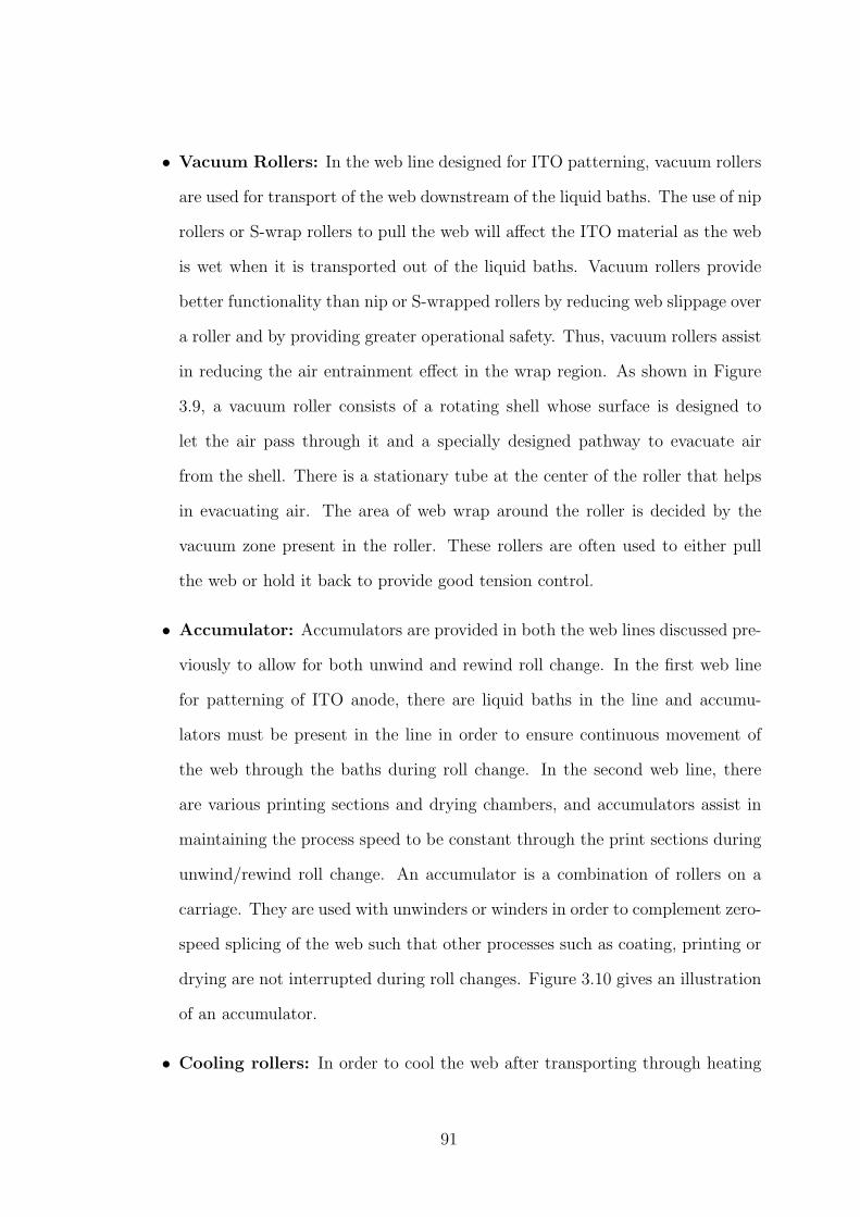
• Vacuum Rollers: In the web line designed for ITO patterning, vacuum rollers
are used for transport of the web downstream of the liquid baths. The use of nip
rollers or S-wrap rollers to pull the web will affect the ITO material as the web
is wet when it is transported out of the liquid baths. Vacuum rollers provide
better functionality than nip or S-wrapped rollers by reducing web slippage over
a roller and by providing greater operational safety. Thus, vacuum rollers assist
in reducing the air entrainment effect in the wrap region. As shown in Figure
3.9, a vacuum roller consists of a rotating shell whose surface is designed to
let the air pass through it and a specially designed pathway to evacuate air
from the shell. There is a stationary tube at the center of the roller that helps
in evacuating air. The area of web wrap around the roller is decided by the
vacuum zone present in the roller. These rollers are often used to either pull
the web or hold it back to provide good tension control.
• Accumulator: Accumulators are provided in both the web lines discussed pre-
viously to allow for both unwind and rewind roll change. In the first web line
for patterning of ITO anode, there are liquid baths in the line and accumu-
lators must be present in the line in order to ensure continuous movement of
the web through the baths during roll change. In the second web line, there
are various printing sections and drying chambers, and accumulators assist in
maintaining the process speed to be constant through the print sections during
unwind/rewind roll change. An accumulator is a combination of rollers on a
carriage. They are used with unwinders or winders in order to complement zero-
speed splicing of the web such that other processes such as coating, printing or
drying are not interrupted during roll changes. Figure 3.10 gives an illustration
of an accumulator.
• Cooling rollers: In order to cool the web after transporting through heating
91
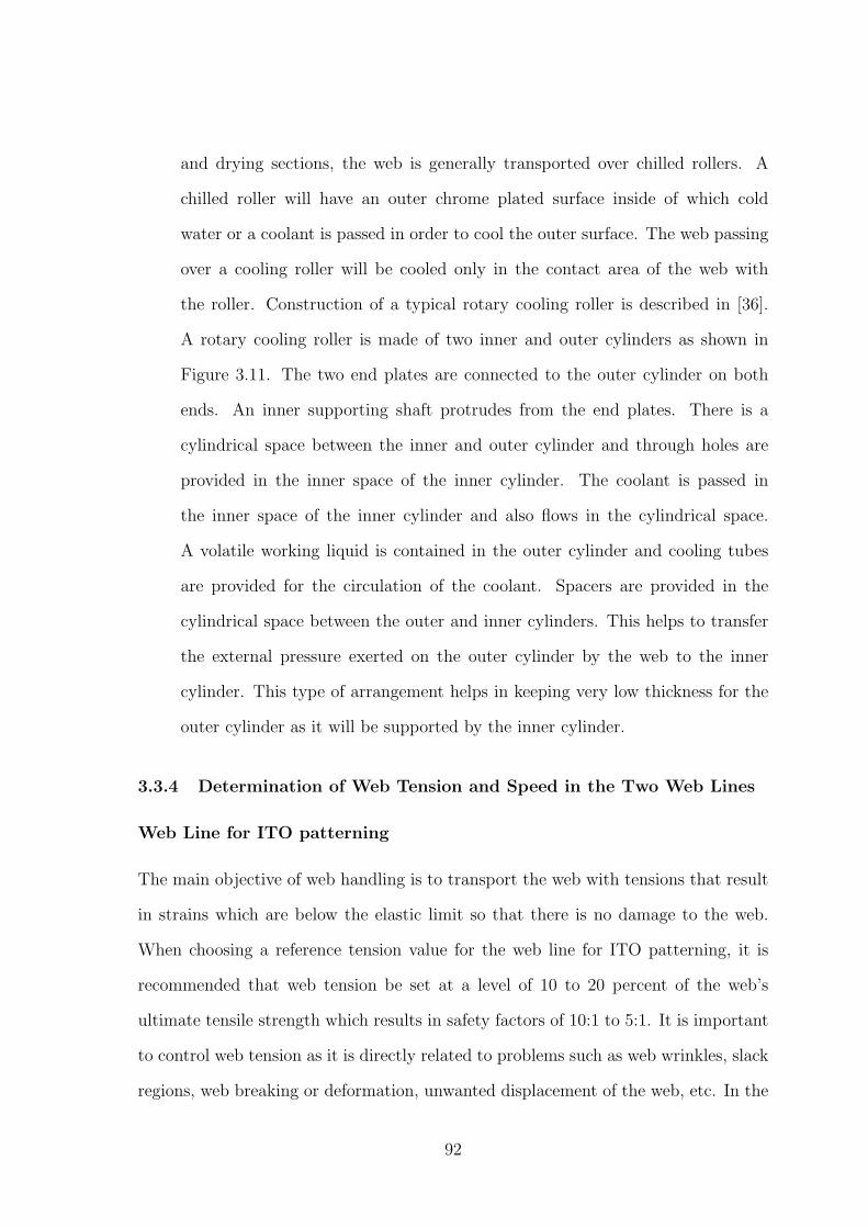
and drying sections, the web is generally transported over chilled rollers. A
chilled roller will have an outer chrome plated surface inside of which cold
water or a coolant is passed in order to cool the outer surface. The web passing
over a cooling roller will be cooled only in the contact area of the web with
the roller. Construction of a typical rotary cooling roller is described in [36].
A rotary cooling roller is made of two inner and outer cylinders as shown in
Figure 3.11. The two end plates are connected to the outer cylinder on both
ends. An inner supporting shaft protrudes from the end plates. There is a
cylindrical space between the inner and outer cylinder and through holes are
provided in the inner space of the inner cylinder. The coolant is passed in
the inner space of the inner cylinder and also flows in the cylindrical space.
A volatile working liquid is contained in the outer cylinder and cooling tubes
are provided for the circulation of the coolant. Spacers are provided in the
cylindrical space between the outer and inner cylinders. This helps to transfer
the external pressure exerted on the outer cylinder by the web to the inner
cylinder. This type of arrangement helps in keeping very low thickness for the
outer cylinder as it will be supported by the inner cylinder.
3.3.4 Determination of Web Tension and Speed in the Two Web Lines
Web Line for ITO patterning
The main objective of web handling is to transport the web with tensions that result
in strains which are below the elastic limit so that there is no damage to the web.
When choosing a reference tension value for the web line for ITO patterning, it is
recommended that web tension be set at a level of 10 to 20 percent of the web’s
ultimate tensile strength which results in safety factors of 10:1 to 5:1. It is important
to control web tension as it is directly related to problems such as web wrinkles, slack
regions, web breaking or deformation, unwanted displacement of the web, etc. In the
92
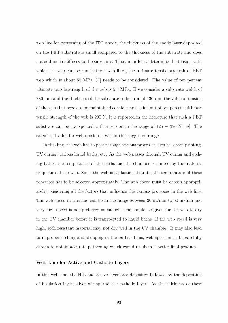
web line for patterning of the ITO anode, the thickness of the anode layer deposited
on the PET substrate is small compared to the thickness of the substrate and does
not add much stiffness to the substrate. Thus, in order to determine the tension with
which the web can be run in these web lines, the ultimate tensile strength of PET
web which is about 55 MPa [37] needs to be considered. The value of ten percent
ultimate tensile strength of the web is 5.5 MPa. If we consider a substrate width of
280 mm and the thickness of the substrate to be around 130 µm, the value of tension
of the web that needs to be maintained considering a safe limit of ten percent ultimate
tensile strength of the web is 200 N. It is reported in the literature that such a PET
substrate can be transported with a tension in the range of 125 − 376 N [38]. The
calculated value for web tension is within this suggested range.
In this line, the web has to pass through various processes such as screen printing,
UV curing, various liquid baths, etc. As the web passes through UV curing and etch-
ing baths, the temperature of the baths and the chamber is limited by the material
properties of the web. Since the web is a plastic substrate, the temperature of these
processes has to be selected appropriately. The web speed must be chosen appropri-
ately considering all the factors that influence the various processes in the web line.
The web speed in this line can be in the range between 20 m/min to 50 m/min and
very high speed is not preferred as enough time should be given for the web to dry
in the UV chamber before it is transported to liquid baths. If the web speed is very
high, etch resistant material may not dry well in the UV chamber. It may also lead
to improper etching and stripping in the baths. Thus, web speed must be carefully
chosen to obtain accurate patterning which would result in a better final product.
Web Line for Active and Cathode Layers
In this web line, the HIL and active layers are deposited followed by the deposition
of insulation layer, silver wiring and the cathode layer. As the thickness of these
93
layers is small compared to the thickness of the plastic substrate, the tension with
which it should be run during this deposition is same as the tension of the web to
be maintained during the first web line. The thickness of the aluminum layer is
significant when compared to the thickness of the substrate. After the deposition of
the aluminum cathode layer, the PET substrate is wound before it is laminated with
the barrier material. Deposition of the cathode layer will change the modulus of the
composite web by a significant amount. Thus, the tension with which the web has to
be run for lamination of the barrier layers needs to be different.
Table 3.1 shows typical values for various parameters involved in rotary screen
printing, gravure printing and ink jet printing technologies [27]. However, for flexible
electronics, printing speeds are lower compared to the ones given in the table due
to the limitations in the properties of inks used for the layers. There is ongoing
research to optimize the ink quality used in the manufacture of flexible electronic
devices. PEDOT:PSS ink does not dry fast and requires a longer drying chamber
which restricts the speed of the web line.
3.3.5 Encapsulation of Barrier Layer
As discussed earlier, OLED devices require protection against moisture and oxygen
intrusion which would degrade their performance and also reduce their lifetime. For
achieving longer lifetimes from OLED based devices, the values for oxygen and mois-
ture permeability must be less than 10−3 cc/m2/day and 10−6 g/m2/day, respectively
[39]. A number of methods have been considered for encapsulation of the flexible
OLED devices. One such method is by using a barrier layer of inorganic materials
which is coated to the flexible polymer substrates using vacuum deposition methods.
These inorganic layers are made of oxides, nitrides or carbides and are impermeable
to moisture and oxygen diffusion. The main reason for this is that the polymeric
substrate by itself is inherently porous and has high permeability level for oxygen
94
and moisture. Researchers have considered the possibility that even with the coating
of an inorganic barrier layer to polymeric substrate, the required criteria of minimum
permeability levels may not be met for OLED devices. This may be due to intrinsic
holes created during the deposition process or impurities contained during the vac-
uum chamber or those present in the substrate itself. In the case of rigid OLEDs,
encapsulation of the device is made by using a glass or metal lid which provides a
hermetic protection against water and moisture [40]. They cannot be used as en-
capsulation layer for flexible OLEDs because of their rigidity, thickness and heavy
nature.
Encapsulation can be made by many methods such as lamination, coating or any
other vacuum deposition methods. Lamination method is preferred as it can be easily
performed using roll to roll form of manufacturing, which will reduce the overall cost
and also results in the manufacturing of flexible devices. Lamination can be done
using different methods such as adhesive lamination, extrusion coating, etc. In the
following section, different methods of lamination will be discussed briefly.
Adhesive lamination can be achieved by dry bonding, wet bonding, UV/EB curing
and by a hot melt adhesion process. In the extrusion method, two dissimilar materials
such as polymer film, paper or foil are bonded together by using a thin layer of
plastic material. Several polymers layers can be extruded simultaneously followed by
pressing or cooling them together which results in co-extruded materials. In the case
of incompatible layers, thermoplastic adhesive is used as a tie layer for laminating
them together. Table 3.2 (page 106) provides a comparison between mainstream
lamination and coating process [41].
Adhesive lamination is the bonding of two or more substrates with the help of
adhesives. Adhesive lamination can be performed using different methods depending
on the type of adhesive or method of application of adhesive. It is a preferred method
of lamination when the substrates cannot be laminated using the co-extrusion process.
95
A co-extrusion process may thermally damage the substrate. Table 3.3 (page 107)
provides an insight into different types of adhesive lamination [41].
Extrusion is a process of coating and lamination where a resin is formed into a hot
film by melting which is coated onto a substrate. Complete contact is obtained by
passing this coated substrate along with the other substrate to be laminated between
counter rotating heated rolls. The coating is used as an adhesive layer between number
of substrates. The second substrate is laminated onto the first coated substrate when
the extrusion coating is still hot which are pressed together using the pressure rolls.
This extruded layer also acts as a moisture barrier layer.
Similar to the lamination of the solar cells, the composite web produced for OLED
devices has to be laminated on both sides with a barrier layer with the help of an
adhesive. Researches are studying the suitability of barrier materials, adhesives and
methods of encapsulation to an OLED device that would provide a longer life time
to the device with efficient barrier property to oxygen and moisture. The adhesive
material should have faster curing and very low curing temperatures to avoid any
damage to the OLED device. The adhesive layer can be either patterned or deposited
as a continuous layer on top of the cathode. Typical layer thickness of the adhesive
layer must be about 2−20 µm in order to provide firm sealing of the barrier layer.
Rotary screen printing method would be the most suitable method for the deposition
of the adhesive layer as it requires the deposition of a thick layer with high viscosity
inks under low nip pressure.
The lamination of barrier layer to both sides of an OLED device has to be done
using a nip, but the rollers must not be heated as they will affect the already deposited
layers of the device. UV drying of adhesive cannot be done as high temperature might
damage the active layer. In the next chapter, a web line for lamination of barrier
material to a solar cell substrate is designed. Lamination is done at room temperature
using pressure sensitive adhesive which is highly suitable for the encapsulation of
96
electronic devices as no heat or higher temperatures are involved. The same web line
can be used for the lamination of barrier material to the OLED device and other
flexible electronic devices. However, the barrier material used and the parameters
used for lamination would be different as they depend on the material properties.
3.3.6 Registration
Registration is the ability with which multiple layers can be printed on top of each
other on a substrate. It is defined as the process of obtaining accurate alignment
of successful print patterns on the web substrate. In the case of flexible electronics,
few of the layers may be patterned and during the deposition of successive layers
on top of the patterned layers, it is very important that the registration is properly
maintained. There are many ways to obtain registration of subsequent patterns. The
selection of an appropriate method depends on the accuracy needed with regards
to the cost of the equipment. Registration in the machine direction is defined as
the relative difference in distance between the two successive printed patterns. It
measures the superposition of accuracy of each ink when inks for multiple layers are
printed in succession. In the case of flexible electronics, very high accuracy is needed
in the alignment of successive layers when inks for the layers are printed in the web
line. In order to maintain good registration accuracy, registration errors must be
automatically controlled during the printing of successive layers.
If the tension is maintained at a constant desired value in the web span between
two successive printing units, one can expect no registration error. However, in prac-
tical situations there may be several factors such as strain induced web elongation,
mechanically induced disturbances, variations in print cylinder velocities which would
lead to a registration error. Thus, active control of registration error is a must when
printing multiple layers in a web line.
After the patterning of an ITO anode on PET substrate in the first web line,
97
active layers are deposited on it in the second web line. In the second web line where
there is deposition of layers such as HIL, emission layer followed by screen printing of
subsequent layers, high quality registration is required in the longitudinal direction in
order to obtain a quality product. In [42], methods for obtaining accurate registration
by using a registration compensator roller are described. The same method can be
used in the second web line for maintaining registration when the different layers
are printed on the substrate. In the second web line, as the inks are deposited to
form the different layers of the electronic component, it is necessary to align them
accurately in order to obtain a quality device. Gravure printing of the HIL layer is
followed by gravure printing of the emission layer. Gravure printing of the emissive
layer must be aligned with respect to the HIL layer. This can be achieved by using
a compensator roll as mentioned in [42]. During the gravure printing of HIL layer, a
registration flag is printed along the edge of the web. It is followed by the printing of
the emissive layer. In order to obtain accurate alignment of the emissive layer with
the HIL layer, the length of the web between two gravure printing units must be an
integral multiple of circumference of the first gravure cylinder. This is true when
both the print cylinders are suitably aligned. As the substrate is elastic, there will be
an elongation of web which would result in stretching of the printed layer. This will
cause mis-registration which will require active registration control in order to obtain
good quality print of the layers.
As discussed in [42], registration control can be achieved by using a compensator
roll. A compensator roll is provided in the web path between the two printing units.
A registration flag is printed during the gravure printing of emission layer too along
the edge of the web at a proper location. A registration error sensor is placed in
the web line soon after the second printing unit. This sensor measures the distance
between the flags that were printed by the two successive printing units. Depending
on the registration error measured by the sensor, the compensator roll is moved up or
98
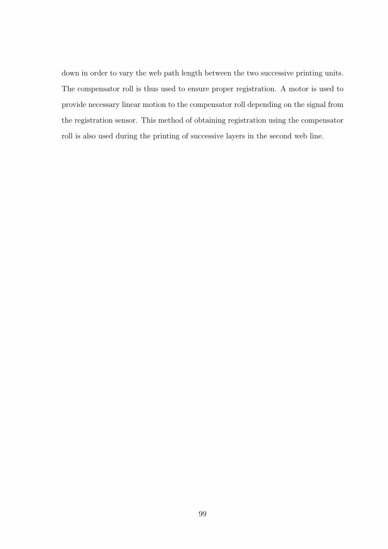
down in order to vary the web path length between the two successive printing units.
The compensator roll is thus used to ensure proper registration. A motor is used to
provide necessary linear motion to the compensator roll depending on the signal from
the registration sensor. This method of obtaining registration using the compensator
roll is also used during the printing of successive layers in the second web line.
99
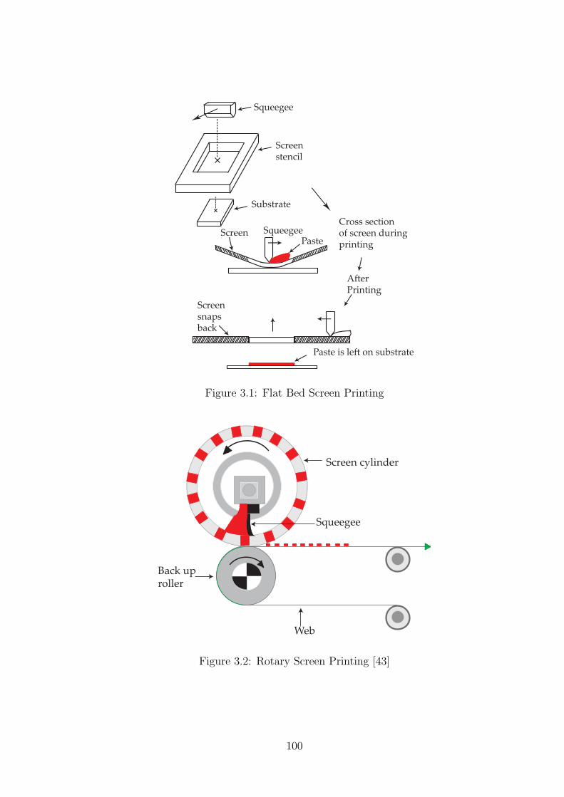
Squeegee
Screen stencil
Substrate
Screen SqueegeePaste
Screensnapsback
Paste is le! on substrate
A!er Printing
Cross sectionof screen duringprinting
Figure 3.1: Flat Bed Screen Printing
Screen cylinder
Squeegee
Back up roller
Web
Figure 3.2: Rotary Screen Printing [43]
100
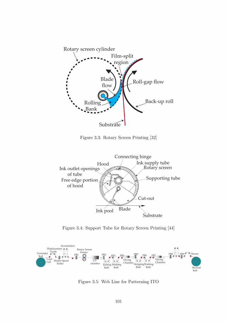
Film-split region
Roll-gap flowBlade flow
Rolling Bank
Substrate
Rotary screen cylinder
Back-up roll
Figure 3.3: Rotary Screen Printing [32]
Ink supply tube
Blade
Rotary screen
Substrate
Supporting tube
Connecting hinge
Cut-out
Free edge portion of hood
HoodInk outlet openings of tube
Ink pool
Figure 3.4: Support Tube for Rotary Screen Printing [44]
Unwinder Roll
Displacement Guide
Accumulator
PR1
Master Speed Roller
Rotary Screen Printer
UV chamber
PR2 PR3 PR4PR5 PR6 PR7
Drying Chamber
Drying Chamber
Etching Bath
Washing Bath
Stripping Bath
Washing Bath
Load Cell
PR9
Rewind Roll
PR8 Sensor
Figure 3.5: Web Line for Patterning ITO
101
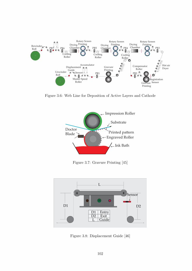
Unwinder Roll
Displacement Guide
Accumulator
PR1 PR2
Master Speed Roller
GravurePrinting
Gravure Printing
Hot airDryer
PR3PR4PR5
Rotary Screen Printing
Rotary Screen Printing
Rotary Screen Printing Drying
ChamberDrying Chamber
Drying Chamber
Cooling Roller
Cooling Roller
PR6PR7
Cooling Roller
Rewinder Roll
Registration Sensor
Compensator Roller
Sensor
Figure 3.6: Web Line for Deposition of Active Layers and Cathode
Doctor Blade
Ink Bath
Engraved Roller
Impression Roller
Substrate
Printed pa!ern
Figure 3.7: Gravure Printing [45]
D2D1
L
Sensor
D1D2L
EntryExit
Guide
Figure 3.8: Displacement Guide [46]
102
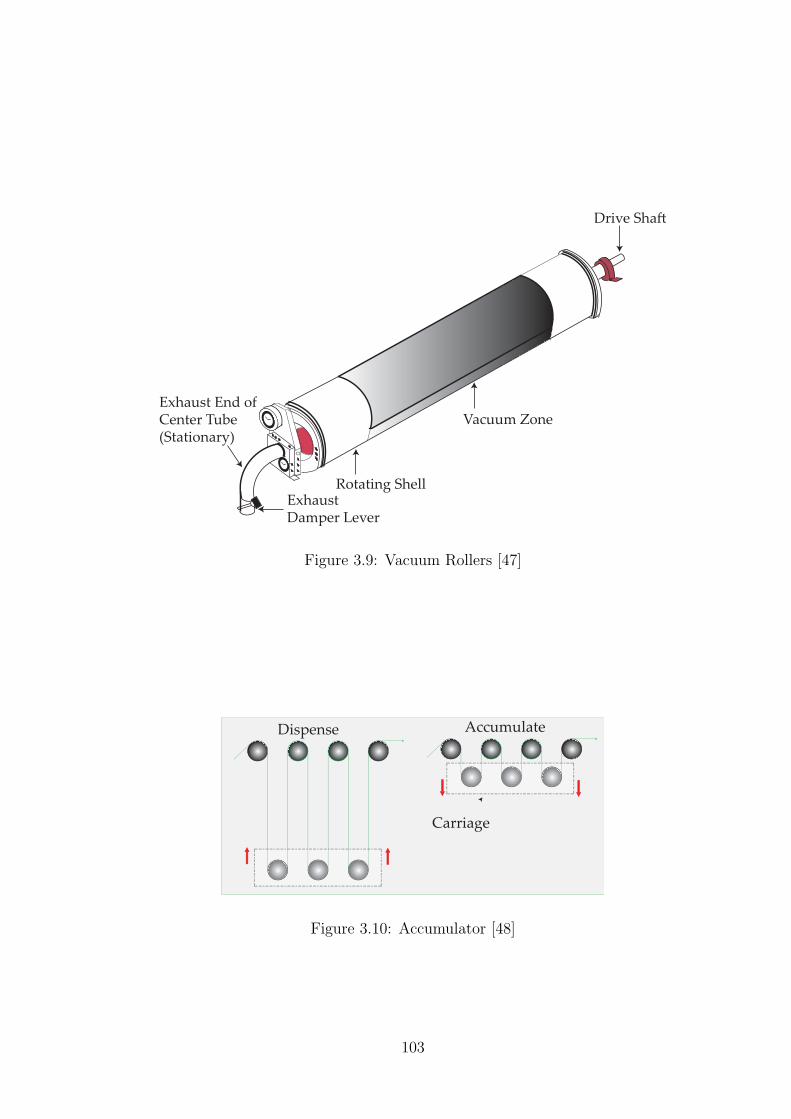
Drive Sha
Vacuum Zone
Rotating ShellExhaust Damper Lever
Exhaust End of Center Tube(Stationary)
Figure 3.9: Vacuum Rollers [47]
Dispense Accumulate
Carriage
Figure 3.10: Accumulator [48]
103
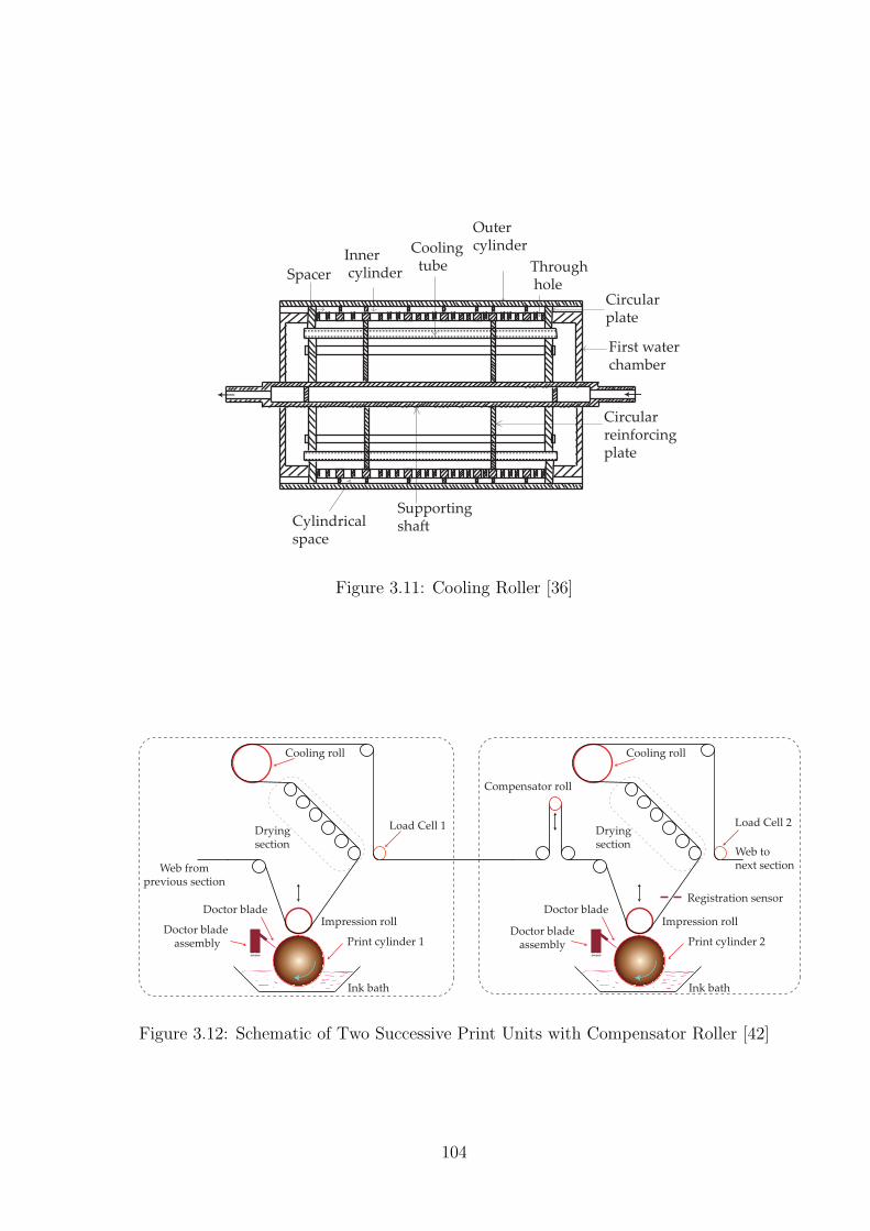
Cylindrical space
Circular plate
Spacer
Inner cylinder
Supporting sha
Through hole
Cooling tube
Outer cylinder
First waterchamber
Circularreinforcingplate
Figure 3.11: Cooling Roller [36]
Load Cell 1 Load Cell 2
Ink bath
Print cylinder 1
Cooling roll
Web fromprevious section
Impression rollDoctor blade
assembly
Doctor blade
Drying section
Ink bath
Print cylinder 2
Registration sensor
Cooling roll
Web to next section
Compensator roll
Impression rollDoctor blade
assembly
Doctor blade
Drying section
Figure 3.12: Schematic of Two Successive Print Units with Compensator Roller [42]
104
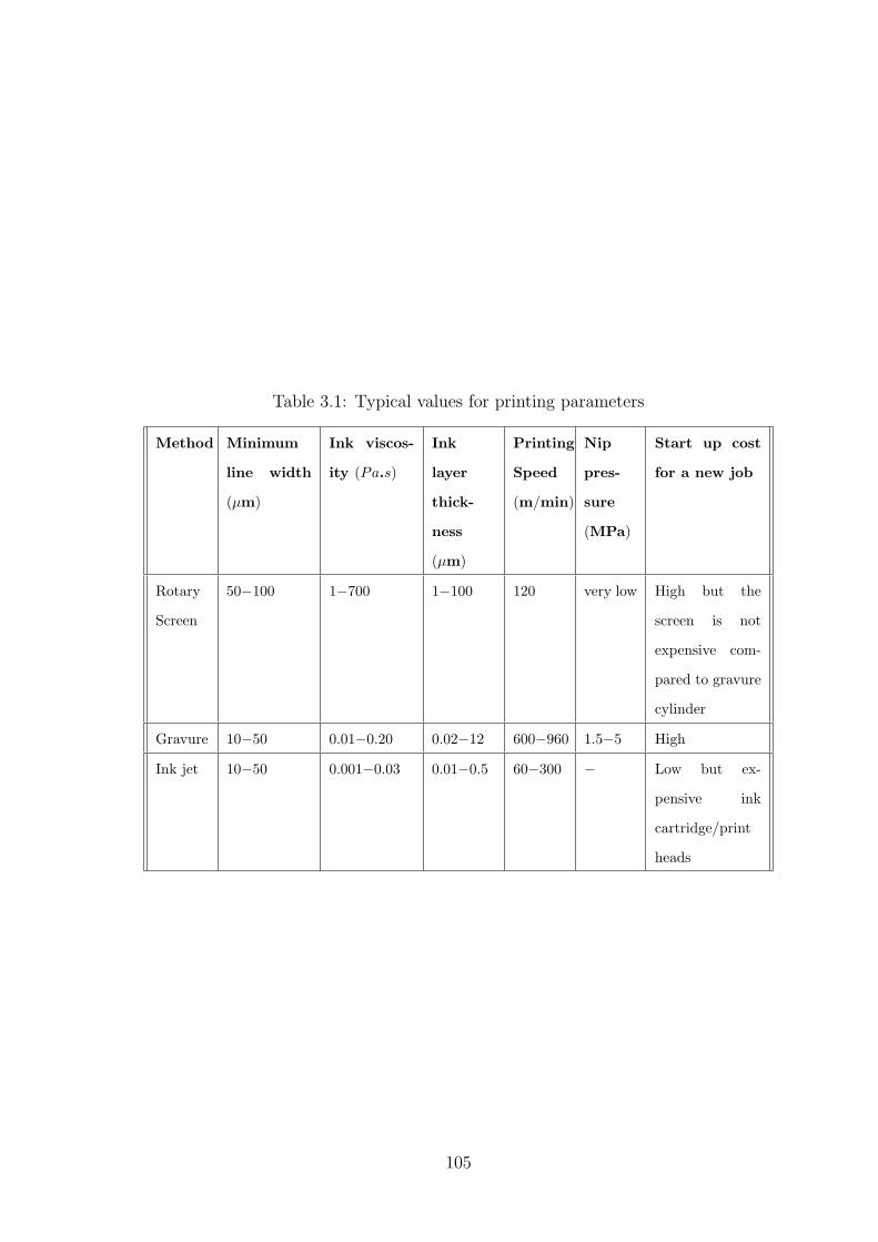
Table 3.1: Typical values for printing parameters
Method Minimum
line width
(µm)
Ink viscos-
ity (Pa.s)
Ink
layer
thick-
ness
(µm)
Printing
Speed
(m/min)
Nip
pres-
sure
(MPa)
Start up cost
for a new job
Rotary
Screen
50−100 1−700 1−100 120 very low High but the
screen is not
expensive com-
pared to gravure
cylinder
Gravure 10−50 0.01−0.20 0.02−12 600−960 1.5−5 High
Ink jet 10−50 0.001−0.03 0.01−0.5 60−300 − Low but ex-
pensive ink
cartridge/print
heads
105
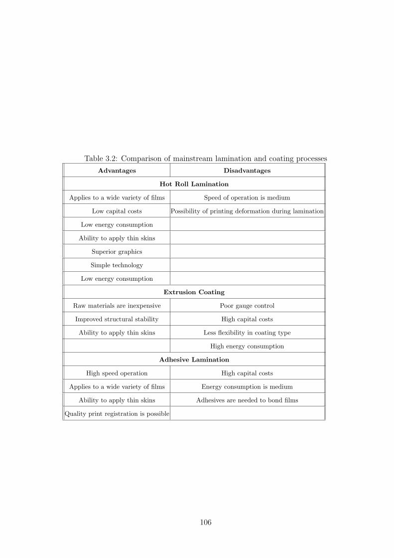
Table 3.2: Comparison of mainstream lamination and coating processes
Advantages Disadvantages
Hot Roll Lamination
Applies to a wide variety of films Speed of operation is medium
Low capital costs Possibility of printing deformation during lamination
Low energy consumption
Ability to apply thin skins
Superior graphics
Simple technology
Low energy consumption
Extrusion Coating
Raw materials are inexpensive Poor gauge control
Improved structural stability High capital costs
Ability to apply thin skins Less flexibility in coating type
High energy consumption
Adhesive Lamination
High speed operation High capital costs
Applies to a wide variety of films Energy consumption is medium
Ability to apply thin skins Adhesives are needed to bond films
Quality print registration is possible
106
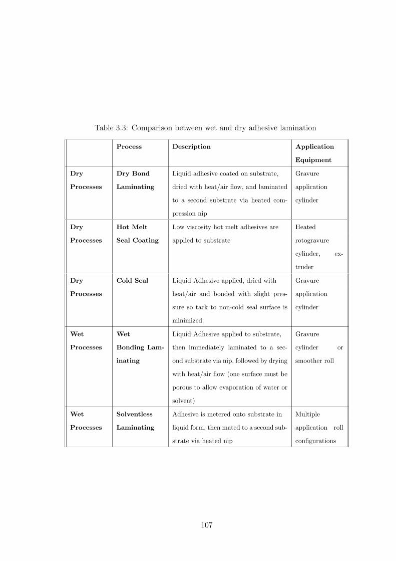
Table 3.3: Comparison between wet and dry adhesive lamination
Process Description Application
Equipment
Dry Dry Bond Liquid adhesive coated on substrate, Gravure
Processes Laminating dried with heat/air flow, and laminated
to a second substrate via heated com-
pression nip
application
cylinder
Dry Hot Melt Low viscosity hot melt adhesives are Heated
Processes Seal Coating applied to substrate rotogravure
cylinder, ex-
truder
Dry Cold Seal Liquid Adhesive applied, dried with Gravure
Processes heat/air and bonded with slight pres-
sure so tack to non-cold seal surface is
minimized
application
cylinder
Wet Wet Liquid Adhesive applied to substrate, Gravure
Processes Bonding Lam-
inating
then immediately laminated to a sec-
ond substrate via nip, followed by drying
with heat/air flow (one surface must be
porous to allow evaporation of water or
solvent)
cylinder or
smoother roll
Wet Solventless Adhesive is metered onto substrate in Multiple
Processes Laminating liquid form, then mated to a second sub-
strate via heated nip
application roll
configurations
107
CHAPTER 4
Modeling and Simulation of Web Lines Designed for Manufacture of
Flexible Electronic Devices
4.1 Introduction
In the first section of this chapter, drag force generated as the web is transported in a
liquid bath is calculated. In the second section, tension and velocity dynamic models
for the web line for patterning of the anode layer on flexible substrate are formulated
and simulations are conducted to regulate web tension and web velocity during its
transport from the unwind roll to the rewind roll. In the third section, a web line for
simultaneous lamination of barrier substrate to the substrate of the flexible electronic
device is designed. Also, a web line is designed for the lamination of adhesive material
to the barrier substrate. In the fourth section, a model for web tension for lamination
of two webs is investigated and simulations are done to regulate web tension and web
velocity across various spans and rollers for the web line designed for lamination of
encapsulation layers.
4.1.1 Calculation of Drag Force on the Web During Transport Through
a Liquid Bath
In RTR manufacturing of flexible panel devices, the substrate is passed through var-
ious processes such as printing, coating, etching, stripping, washing bath, etc. Web
tension and web velocity need to be controlled precisely when transporting the web
through these processes in a web line. When the web is passed through a liquid
bath for operations such as etching, stripping, washing and rinsing, the tension and
108
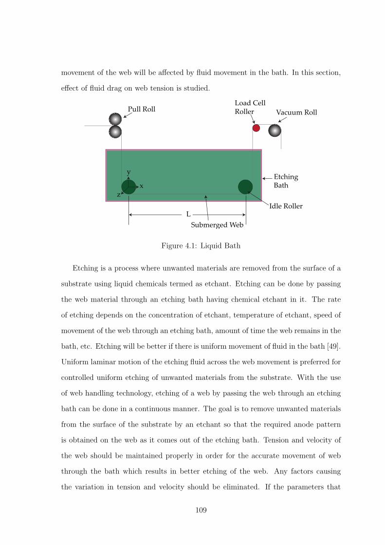
movement of the web will be affected by fluid movement in the bath. In this section,
effect of fluid drag on web tension is studied.
L
xz
yEtching Bath
Pull Roll Vacuum Roll
Load CellRoller
Idle Roller
Submerged Web
Figure 4.1: Liquid Bath
Etching is a process where unwanted materials are removed from the surface of a
substrate using liquid chemicals termed as etchant. Etching can be done by passing
the web material through an etching bath having chemical etchant in it. The rate
of etching depends on the concentration of etchant, temperature of etchant, speed of
movement of the web through an etching bath, amount of time the web remains in the
bath, etc. Etching will be better if there is uniform movement of fluid in the bath [49].
Uniform laminar motion of the etching fluid across the web movement is preferred for
controlled uniform etching of unwanted materials from the substrate. With the use
of web handling technology, etching of a web by passing the web through an etching
bath can be done in a continuous manner. The goal is to remove unwanted materials
from the surface of the substrate by an etchant so that the required anode pattern
is obtained on the web as it comes out of the etching bath. Tension and velocity of
the web should be maintained properly in order for the accurate movement of web
through the bath which results in better etching of the web. Any factors causing
the variation in tension and velocity should be eliminated. If the parameters that
109
cause tension variation or affect the velocity of the web cannot be eliminated, then
compensation should be provided for such variations.
As the web moves through the fluid, it will experience a drag force in opposition
of the movement of the web. This drag force is mainly due to shear stress caused due
to the viscosity of the etchant fluid. The drag force will oppose the free movement of
the web through the etching bath which might affect web tension. The web can be
passed through the liquid bath with the use of rollers [50]. Idle rollers can be placed
inside the liquid bath for guiding the web through it and web is transported into
the bath with the help of a driven roller. Web tension is maintained by using driven
rollers before and after the bath and using suitable tension control systems in either
or both the driven rollers. While considering the tension of the web, effect of drag
force on the tension must be calculated. Based on the drag force calculation, suitable
changes can be made to the governing equation for tension in a web span to account
for fluid drag forces. Over the years, many researchers have studied the effect of fluid
movement on a moving wall. This research has focused on the movement of the fluid
to be either in the direction of the moving wall or opposite to the direction of the
moving wall. In the year 1997, P.D. Weidman [51] formulated the shear stress on the
moving wall by laminar fluid flow in the cross flow direction. All the problems with
respect to moving wall in the fluid are considered to be boundary value problems and
solution was found using Blasius similarity variable conditions.
4.1.2 Drag Force Calculation
Consider the Cartesian coordinates (x,y,z) as shown in the Figure 4.1. Let the web be
moving in the direction of x-axis and let the span wise fluid flow be in the z-direction
and y be the direction normal to both these axes. Let u, v, w be the components of
velocity in the x, y and z directions respectively. In this problem formulation, fluid
density and viscosity of the fluid are assumed to be constant. It is assumed that there
110
is uniform steady flow in the cross wise direction. It is assumed that all flows are
of infinite extent in the z-direction and thus fully developed. It is also assumed that
the pressure gradient in the web direction and in the crosswise direction are zero.
Therefore the Navier Stoke equations can be written as follows [51]:
∂u
∂x+∂v
∂y= 0 (4.1)
u∂u
∂x+ v
∂v
∂y= ν
∂2u
∂y2(4.2)
u∂w
∂x+ v
∂w
∂y= ν
∂2w
∂y2(4.3)
Application of Blasius similarity form gives the following similarity conditions:
ψ(x, y) =√
2νU0xf(η) (4.4)
η =
√
U0
2νxy (4.5)
The similarity function f(η) is found by solving the Blasius boundary value prob-
lem which satisfies the following differential equation:
f ′′′ + ff ′′ = 0 (4.6)
f(0) = 0 (4.7)
f ′(0) = λ (4.8)
f ′(η → ∞) = 1 (4.9)
When there is uniform cross flow above the moving web, the similarity form can
be given as follows [51]:
s′′ + fs′ = 0 (4.10)
s(0) = 0 (4.11)
s(η → ∞) = 1 (4.12)
111
The shear stress for a fluid flowing in the span wise direction to the moving plate
can be calculated using the following equation [51].
τ =
√
νU0
2x[U0f
′′(0)i+W0s′(0)k] (4.13)
In the above equation, the first term on the right hand side gives the component
of shear stress in the x-direction and second term on the right hand side equation
gives the component of shear stress in the z direction. So, it is the component in the
x-direction that opposes the motion of the web through the bath. The drag force can
be calculated by substituting the value of shear stress obtained using (4.13) in the
equation (4.14).
Fd = W
∫ L
0
τ(x)dx (4.14)
where the integration is from x = 0 to x = L. This drag force acts in the direction
opposite to web motion and opposes the motion of web through the bath. In the
liquid bath, since there is no fluid movement in the x-direction,
λ =U∞
Uw
= 0 (4.15)
Assuming that there is negligible fluid motion in the direction of the web movement
results in
U0 = Uw + U∞ = Uw (4.16)
The value of f ′′(0) and s′(0) in the equation (4.13) for calculating the shear stress
value can be found by solving the Blasius boundary value equations which are given
by (4.6) and (4.10). To solve the equation (4.6) which is of third order, only two
initial and one final boundary conditions are given. Since it is difficult to use the
final boundary condition to solve this equation, a random initial value for f ′′(0) is
assumed and a shooting method is used to find a suitable value that would fit f ′′(0)
which would satisfy the final condition given by the equation (4.9). Similarly, even
the value for s′(0) is calculated such that it satisfies the boundary condition given in
the equation (4.12).
112
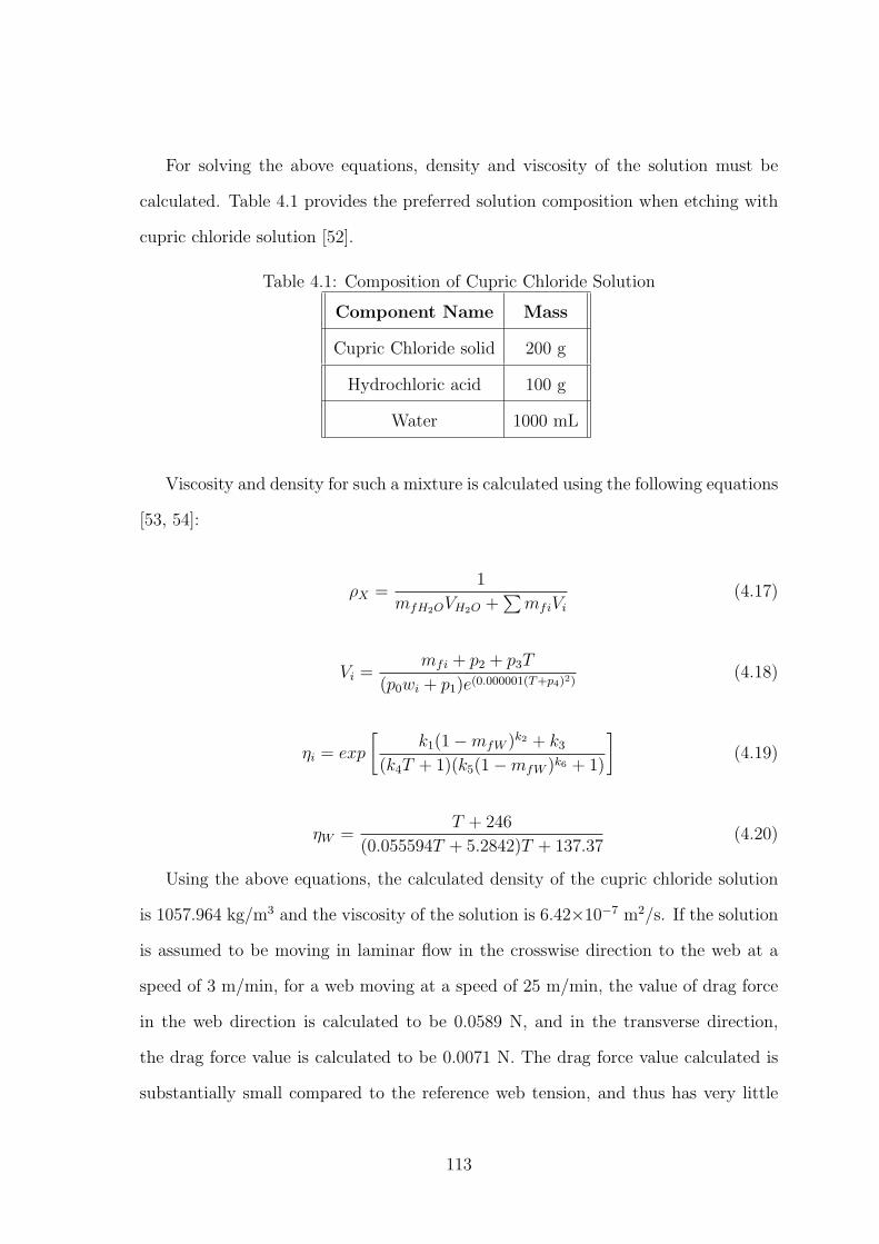
For solving the above equations, density and viscosity of the solution must be
calculated. Table 4.1 provides the preferred solution composition when etching with
cupric chloride solution [52].
Table 4.1: Composition of Cupric Chloride Solution
Component Name Mass
Cupric Chloride solid 200 g
Hydrochloric acid 100 g
Water 1000 mL
Viscosity and density for such a mixture is calculated using the following equations
[53, 54]:
ρX =1
mfH2OVH2O +∑
mfiVi(4.17)
Vi =mfi + p2 + p3T
(p0wi + p1)e(0.000001(T+p4)2)(4.18)
ηi = exp
[
k1(1−mfW )k2 + k3(k4T + 1)(k5(1−mfW )k6 + 1)
]
(4.19)
ηW =T + 246
(0.055594T + 5.2842)T + 137.37(4.20)
Using the above equations, the calculated density of the cupric chloride solution
is 1057.964 kg/m3 and the viscosity of the solution is 6.42×10⁻⁷ m2/s. If the solution
is assumed to be moving in laminar flow in the crosswise direction to the web at a
speed of 3 m/min, for a web moving at a speed of 25 m/min, the value of drag force
in the web direction is calculated to be 0.0589 N, and in the transverse direction,
the drag force value is calculated to be 0.0071 N. The drag force value calculated is
substantially small compared to the reference web tension, and thus has very little
113
effect on the behavior of the web. The same condition applies when it is passed
through other liquid baths as laminar movement of fluid in the crosswise direction is
preferred.
4.2 Modeling and Simulation of the Web Line for Patterning of the
Anode Layer on PET Substrate
The web line is a dynamic system with various control zones to control the movement
of the web as it passes thorough different process sections. In the simulation of the
web line, a speed-based tension control system is employed. This type of control
strategy involves a two loop system in which the tension measuring device such as
load cells provide the tension feedback based on which the outer tension loop provides
correction to the inside velocity loop.
In the previous chapter, a web line for patterning of ITO anode layer on a PET
substrate is designed. In this section, tension and velocity dynamic models are for-
mulated for the same line and simulations are conducted to regulate web tension and
velocity as it passes through various sections for patterning of anode material.
The designed web line consists of an unwind roll, unwind/rewind accumulators,
several web spans supported by driven/idle rollers, screen printer, UV chamber, cool-
ing rolls, various liquid baths, drying chambers, etc. It is very important to control
the tension of the web as it is transported from the unwind to the rewind section
having various process sections between them. Thus, it is necessary to control the
speed of the unwind roller, rewind roller and all the driven rollers of the web line so
that the tension and velocity of the web will be maintained at the necessary reference
values. Except for one of the driven rollers which is termed as the master speed roller,
all the other driven rollers are used to regulate both web velocity and web tension in
their respective spans. The master speed roller is used to regulate web velocity only,
and effectively sets the line speed. The motor controller used for driving the master
114
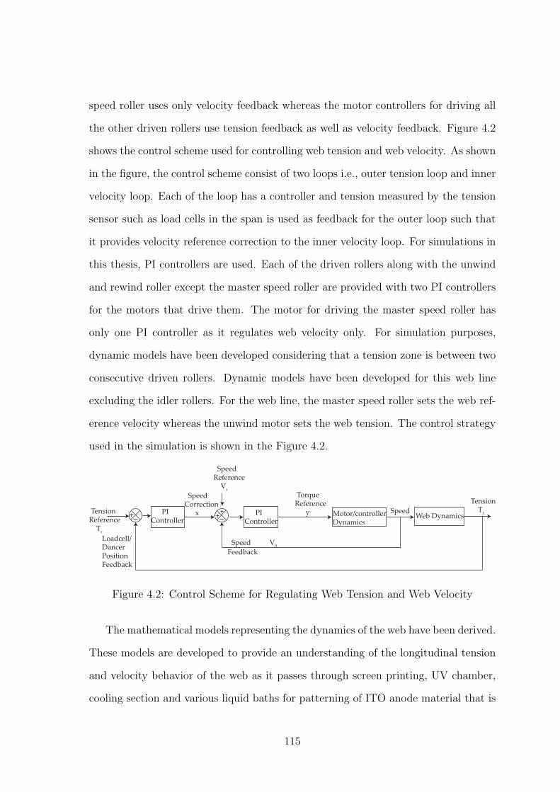
speed roller uses only velocity feedback whereas the motor controllers for driving all
the other driven rollers use tension feedback as well as velocity feedback. Figure 4.2
shows the control scheme used for controlling web tension and web velocity. As shown
in the figure, the control scheme consist of two loops i.e., outer tension loop and inner
velocity loop. Each of the loop has a controller and tension measured by the tension
sensor such as load cells in the span is used as feedback for the outer loop such that
it provides velocity reference correction to the inner velocity loop. For simulations in
this thesis, PI controllers are used. Each of the driven rollers along with the unwind
and rewind roller except the master speed roller are provided with two PI controllers
for the motors that drive them. The motor for driving the master speed roller has
only one PI controller as it regulates web velocity only. For simulation purposes,
dynamic models have been developed considering that a tension zone is between two
consecutive driven rollers. Dynamic models have been developed for this web line
excluding the idler rollers. For the web line, the master speed roller sets the web ref-
erence velocity whereas the unwind motor sets the web tension. The control strategy
used in the simulation is shown in the Figure 4.2.
PI Controller
Motor/controllerDynamics
Web Dynamics
Torque Reference y Speed
Tension T
1
Speed
Feedback
V0
Loadcell/DancerPositionFeedback
TensionReference T
r
SpeedReference V
r
SpeedCorrection x PI
Controller
Figure 4.2: Control Scheme for Regulating Web Tension and Web Velocity
The mathematical models representing the dynamics of the web have been derived.
These models are developed to provide an understanding of the longitudinal tension
and velocity behavior of the web as it passes through screen printing, UV chamber,
cooling section and various liquid baths for patterning of ITO anode material that is
115
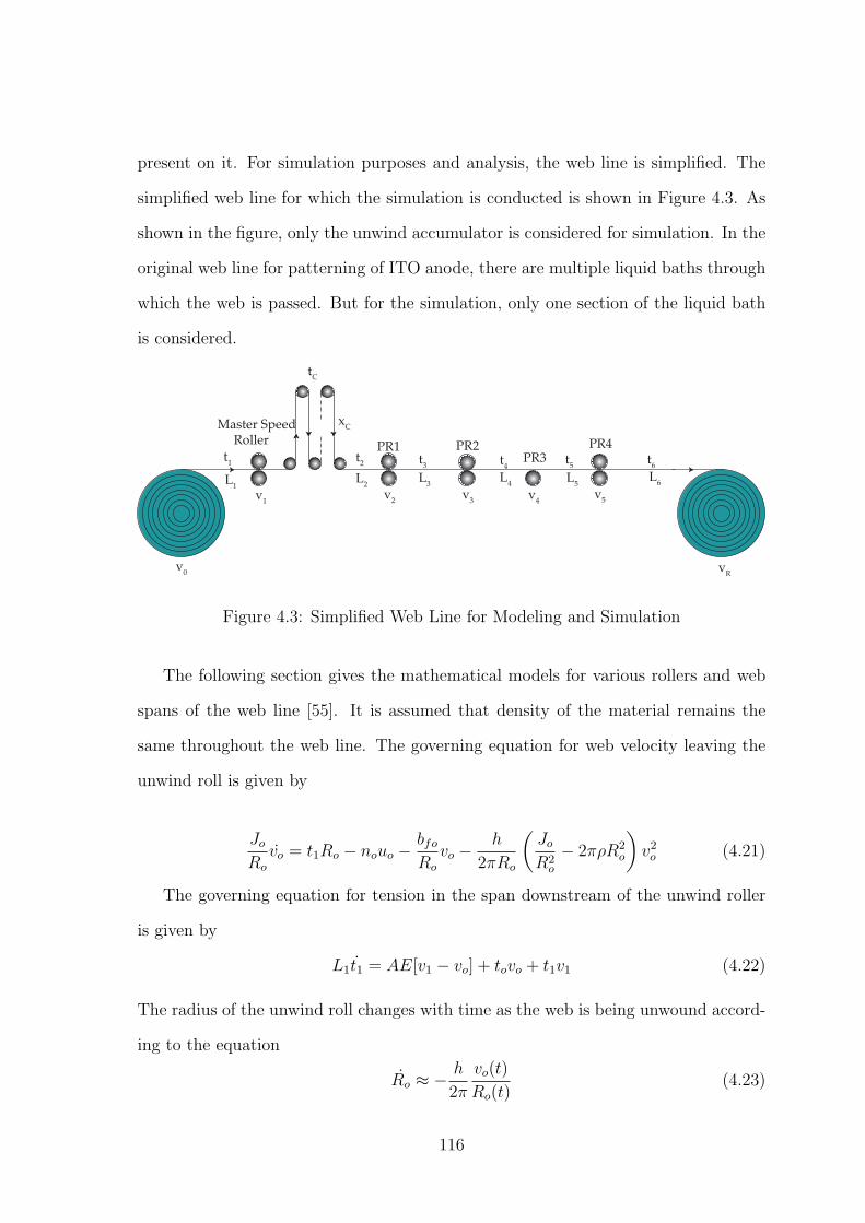
present on it. For simulation purposes and analysis, the web line is simplified. The
simplified web line for which the simulation is conducted is shown in Figure 4.3. As
shown in the figure, only the unwind accumulator is considered for simulation. In the
original web line for patterning of ITO anode, there are multiple liquid baths through
which the web is passed. But for the simulation, only one section of the liquid bath
is considered.
Master Speed Roller
PR1 PR2PR3
PR4t
1 t6
t5t
4t
3
tC
L1
L6L
5L
4L
3
xC
v0
v1
v2
v3
v4
v5
vR
t2
L2
Figure 4.3: Simplified Web Line for Modeling and Simulation
The following section gives the mathematical models for various rollers and web
spans of the web line [55]. It is assumed that density of the material remains the
same throughout the web line. The governing equation for web velocity leaving the
unwind roll is given by
JoRo
vo = t1Ro − nouo −bfoRo
vo −h
2πRo
(
JoR2
o
− 2πρR2o
)
v2o (4.21)
The governing equation for tension in the span downstream of the unwind roller
is given by
L1t1 = AE[v1 − vo] + tovo + t1v1 (4.22)
The radius of the unwind roll changes with time as the web is being unwound accord-
ing to the equation
Ro ≈ −h
2π
vo(t)
Ro(t)(4.23)
116
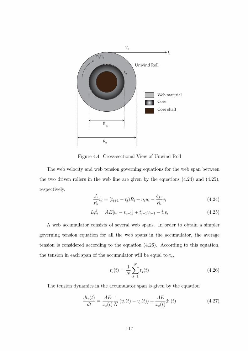
R0
Rc0
t0
t1
v0
n0u
0
Unwind Roll
Core sha!
Core
Web material
Figure 4.4: Cross-sectional View of Unwind Roll
The web velocity and web tension governing equations for the web span between
the two driven rollers in the web line are given by the equations (4.24) and (4.25),
respectively.
JiRi
vi = (ti+1 − ti)Ri + niui −bfiRi
vi (4.24)
Liti = AE[vi − vi−1] + ti−1vi−1 − tivi (4.25)
A web accumulator consists of several web spans. In order to obtain a simpler
governing tension equation for all the web spans in the accumulator, the average
tension is considered according to the equation (4.26). According to this equation,
the tension in each span of the accumulator will be equal to tc.
tc(t) =1
N
N∑
j=1
tj(t) (4.26)
The tension dynamics in the accumulator span is given by the equation
dtc(t)
dt=
AE
xc(t)
1
N(ve(t)− vp(t)) +
AE
xc(t)xc(t) (4.27)
117
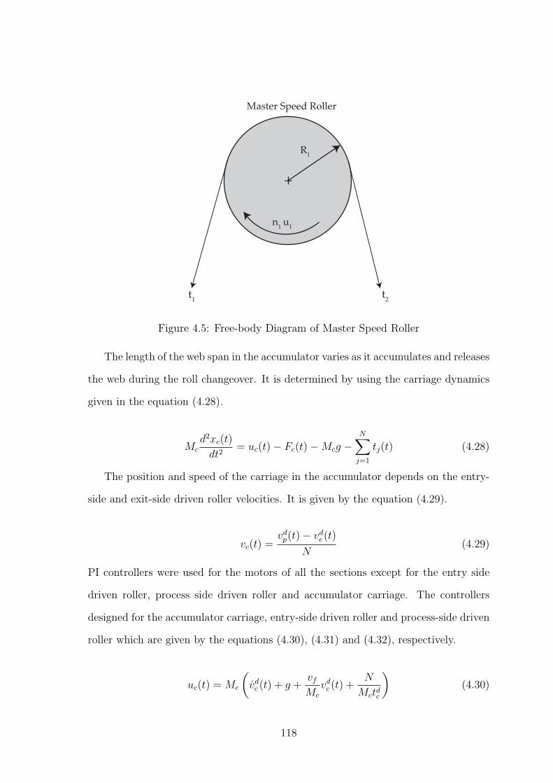
Master Speed Roller
t1
t2
R1
u1
n1
Figure 4.5: Free-body Diagram of Master Speed Roller
The length of the web span in the accumulator varies as it accumulates and releases
the web during the roll changeover. It is determined by using the carriage dynamics
given in the equation (4.28).
Mc
d2xc(t)
dt2= uc(t)− Fc(t)−Mcg −
N∑
j=1
tj(t) (4.28)
The position and speed of the carriage in the accumulator depends on the entry-
side and exit-side driven roller velocities. It is given by the equation (4.29).
vc(t) =vdp(t)− vde(t)
N(4.29)
PI controllers were used for the motors of all the sections except for the entry side
driven roller, process side driven roller and accumulator carriage. The controllers
designed for the accumulator carriage, entry-side driven roller and process-side driven
roller which are given by the equations (4.30), (4.31) and (4.32), respectively.
uc(t) =Mc
(
vdc (t) + g +vfMc
vdc (t) +N
Mctdc
)
(4.30)
118
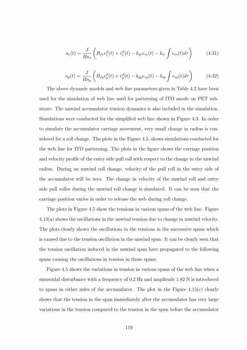
ue(t) =J
Rne
(
Bfevde(t) + vde(t)− kpeeve(t)− kie
∫
eve(t)dτ
)
(4.31)
up(t) =J
Rnp
(
Bfpvdp(t) + vdp(t)− kppevp(t)− kip
∫
evp(t)dτ
)
(4.32)
The above dynamic models and web line parameters given in Table 4.2 have been
used for the simulation of web line used for patterning of ITO anode on PET sub-
strate. The unwind accumulator tension dynamics is also included in the simulation.
Simulations were conducted for the simplified web line shown in Figure 4.3. In order
to simulate the accumulator carriage movement, very small change in radius is con-
sidered for a roll change. The plots in the Figure 4.5, shows simulations conducted for
the web line for ITO patterning. The plots in the figure shows the carriage position
and velocity profile of the entry side pull roll with respect to the change in the unwind
radius. During an unwind roll change, velocity of the pull roll in the entry side of
the accumulator will be zero. The change in velocity of the unwind roll and entry
side pull roller during the unwind roll change is simulated. It can be seen that the
carriage position varies in order to release the web during roll change.
The plots in Figure 4.5 show the tensions in various spans of the web line. Figure
4.13(a) shows the oscillations in the unwind tension due to change in unwind velocity.
The plots clearly shows the oscillations in the tensions in the successive spans which
is caused due to the tension oscillation in the unwind span. It can be clearly seen that
the tension oscillation induced in the unwind span have propagated to the following
spans causing the oscillations in tension in those spans.
Figure 4.5 shows the variations in tension in various spans of the web line when a
sinusoidal disturbance with a frequency of 0.2 Hz and amplitude 1.82 N is introduced
to spans in either sides of the accumulator. The plot in the Figure 4.15(c) clearly
shows that the tension in the span immediately after the accumulator has very large
variations in the tension compared to the tension in the span before the accumulator
119
(Figure 4.15(a)). This is caused by the variations in accumulator span tension. Since
the accumulator span tension is not controlled, the variation in the accumulator span
tension magnifies the tension disturbances in the span immediately downstream of
the accumulator. This tension variation propagates to the following spans but will
be eventually attenuated in successive spans. Thus, it is very important to have good
control of tension before the accumulator spans.
Figure 4.5 represents tension variations in the various spans of the web line, when a
sinusoidal disturbance of amplitude 0.25 m/s2 and frequency of 0.5 Hz is introduced
into the accumulator carriage dynamics. Low frequency disturbances are used as
they are typical disturbances in the accumulator carriage [56]. It can be clearly
seen that the propagation of tension disturbances to the spans downstream of the
accumulator. The plots in the Figure 4.5 show the reduction in the tension variations
in the successive spans downstream of the accumulator.
4.3 Tension Models for Lamination of Webs
In this section, tension dynamics for lamination of two webs using a nip roller is
described [57]. In order to determine the tension dynamics, the mechanical and
physical properties must be developed for the laminated web material which is derived
by using the rule of mixtures. To determine the elastic modulus of a laminated web,
constant stress or constant strain condition can be used. As the laminated material
is required to have a uniform displacement in the longitudinal direction in order to
obtain perfect bonding between the webs and also to avoid the problems such as
curling of the laminated web, constant strain condition is used for determining the
modulus of elasticity of the laminated web in the machine direction. In order to
formulate the tension dynamics, consider the web lamina made of two materials A
and B as shown in Figure 4.6. In this formulation, the width of the webs to be
laminated are considered to be the same. The total stress experienced by the lamina
120
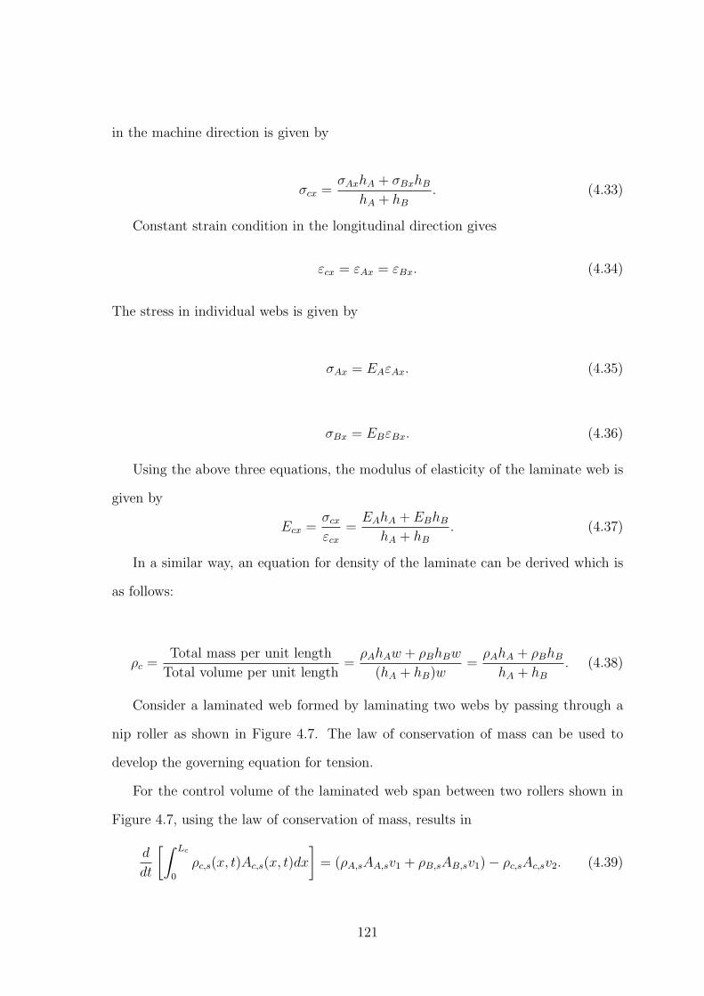
in the machine direction is given by
σcx =σAxhA + σBxhB
hA + hB. (4.33)
Constant strain condition in the longitudinal direction gives
εcx = εAx = εBx. (4.34)
The stress in individual webs is given by
σAx = EAεAx. (4.35)
σBx = EBεBx. (4.36)
Using the above three equations, the modulus of elasticity of the laminate web is
given by
Ecx =σcxεcx
=EAhA + EBhB
hA + hB. (4.37)
In a similar way, an equation for density of the laminate can be derived which is
as follows:
ρc =Total mass per unit length
Total volume per unit length=ρAhAw + ρBhBw
(hA + hB)w=ρAhA + ρBhBhA + hB
. (4.38)
Consider a laminated web formed by laminating two webs by passing through a
nip roller as shown in Figure 4.7. The law of conservation of mass can be used to
develop the governing equation for tension.
For the control volume of the laminated web span between two rollers shown in
Figure 4.7, using the law of conservation of mass, results in
d
dt
[∫ Lc
0
ρc,s(x, t)Ac,s(x, t)dx
]
= (ρA,sAA,sv1 + ρB,sAB,sv1)− ρc,sAc,sv2. (4.39)
121
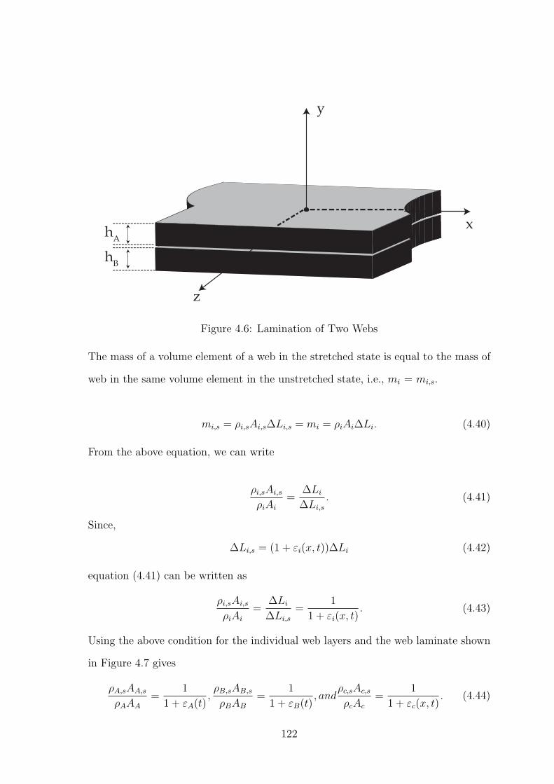
hA
hB
y
x
z
Figure 4.6: Lamination of Two Webs
The mass of a volume element of a web in the stretched state is equal to the mass of
web in the same volume element in the unstretched state, i.e., mi = mi,s.
mi,s = ρi,sAi,s∆Li,s = mi = ρiAi∆Li. (4.40)
From the above equation, we can write
ρi,sAi,s
ρiAi
=∆Li
∆Li,s
. (4.41)
Since,
∆Li,s = (1 + εi(x, t))∆Li (4.42)
equation (4.41) can be written as
ρi,sAi,s
ρiAi
=∆Li
∆Li,s
=1
1 + εi(x, t). (4.43)
Using the above condition for the individual web layers and the web laminate shown
in Figure 4.7 gives
ρA,sAA,s
ρAAA
=1
1 + εA(t),ρB,sAB,s
ρBAB
=1
1 + εB(t), and
ρc,sAc,s
ρcAc
=1
1 + εc(x, t). (4.44)
122
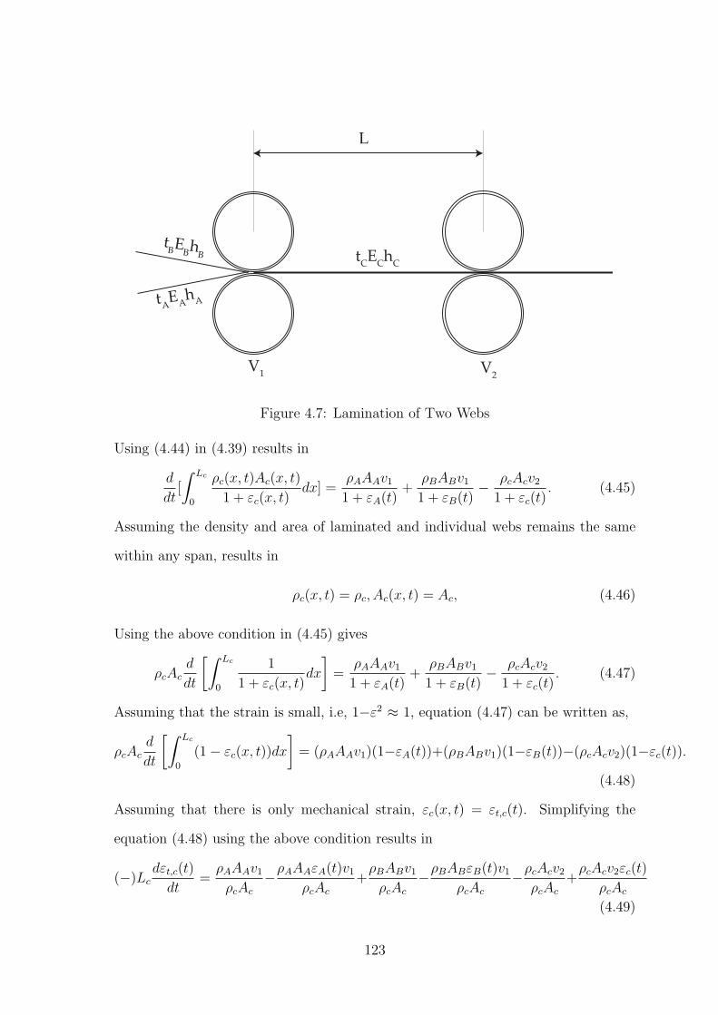
L
V1 V
2
tCE
Ch
C
tBE
BhB
tAEA
hA
Figure 4.7: Lamination of Two Webs
Using (4.44) in (4.39) results in
d
dt[
∫ Lc
0
ρc(x, t)Ac(x, t)
1 + εc(x, t)dx] =
ρAAAv11 + εA(t)
+ρBABv11 + εB(t)
−ρcAcv21 + εc(t)
. (4.45)
Assuming the density and area of laminated and individual webs remains the same
within any span, results in
ρc(x, t) = ρc, Ac(x, t) = Ac, (4.46)
Using the above condition in (4.45) gives
ρcAc
d
dt
[∫ Lc
0
1
1 + εc(x, t)dx
]
=ρAAAv11 + εA(t)
+ρBABv11 + εB(t)
−ρcAcv21 + εc(t)
. (4.47)
Assuming that the strain is small, i.e, 1−ε2 ≈ 1, equation (4.47) can be written as,
ρcAc
d
dt
[∫ Lc
0
(1− εc(x, t))dx
]
= (ρAAAv1)(1−εA(t))+(ρBABv1)(1−εB(t))−(ρcAcv2)(1−εc(t)).
(4.48)
Assuming that there is only mechanical strain, εc(x, t) = εt,c(t). Simplifying the
equation (4.48) using the above condition results in
(−)Lc
dεt,c(t)
dt=ρAAAv1ρcAc
−ρAAAεA(t)v1
ρcAc
+ρBABv1ρcAc
−ρBABεB(t)v1
ρcAc
−ρcAcv2ρcAc
+ρcAcv2εc(t)
ρcAc
(4.49)
123
Simplifying the above equation gives
Lc
dεt,c(t)
dt= (v2 − v1) +
(
ρAhAεA(t) + ρBhBεB(t)
ρAhA + ρBhB
)
v1 − v2εc(t) (4.50)
Replacing the velocity term by average velocity in the terms involving the product
of strain and velocity in (4.50) gives
Lc
dεt,c(t)
dt= (v2 − v1) +
(
ρAhAεt,A(t) + ρBhBεt,B(t)
ρAhA + ρBhB
)
v − vεt,c(t) (4.51)
The governing equation for web tension can be obtained by assuming a constitutive
relation between web strain and web tension. By assuming the individual layers as
well as the laminated web to be linearly elastic,
εt,c(t) =tc(t)
EcAc
, εt,A(t) =tA(t)
EAAA
and εt,B(t) =tB(t)
EBAB
(4.52)
Using the above condition given in (4.52) in (4.51), the governing equation for
web tension in the laminated web span can be written as
dtcdt
=EcAc
Lc
(v2 − v1) +EcAc
Lc
(
ρAhA
EAAA
tA + ρBhB
EBAB
tB
ρAhA + ρBhB
)
v −vtcLc
(4.53)
Using the condition in (4.37) and area A = (hA+hB)w in the above equation and
simplifying gives
dtcdt
=(EAhA + EBhB)
Lc
w(v2 − v1)−vtcLc
+v
Lc
(
EAhA + EBhBEAhA
)(
ρAhAtAρAhA + ρBhB
)
+v
Lc
(
EAhA + EBhBEBhB
)(
ρBhBtBρAhA + ρBhB
)
(4.54)
The above tension dynamic model for the laminated web can be applied for the
lamination of any number of webs. In the lamination of barrier material to the flexible
electronic component, this tension dynamic model can be used.
124
4.4 Web Line for Barrier Lamination to the Substrate for Flexible
Electronics
During the manufacture of flexible electronic devices such as OLED, solar cell, LCDs,
etc., final encapsulation of the device is important. It is a critical stage in the man-
ufacture of the device. This is due to the fact that encapsulation is done to obtain
barrier against moisture, oxygen and other environmental impermeants. Any wastage
at this stage would be costly. Appropriate selection of barrier materials, encapsula-
tion methods and bonding materials are crucial for the effective functioning of the
final device. It is always better to perform the adhesive and barrier lamination in the
presence of inert atmosphere. This is due to the strict barrier requirements for the
active layers of flexible electronic devices.
A good barrier material that would provide longer life for a flexible OLED device
has not yet been found. Currently, there are active investigations on this topic. The
requirements for the barrier layer for polymer solar cells is not as stringent as in
flexible OLED devices. Therefore, barrier materials for the encapsulation of polymer
solar cells are available, and have been used recently in the manufacture of films for
solar cells. In this section, lamination of barrier material to a flexible solar cell will
be discussed. A web line for lamination has been designed. The same line and similar
lamination methods could be used for the lamination of flexible OLED devices in the
future. A barrier material made of silicon oxide coated PET substrate can be used
for the encapsulation of the solar cell device [17]. However, in this thesis a barrier
material which is better than the barrier material used in [17], has been considered
for lamination of the solar cell device.
When laminating the electronic components with the barrier layer, cold lamina-
tion is preferred as the electronic device substrate will be coated with active layers
prior to its lamination. If heat is involved during lamination, then it would affect
the performance of the device as most of the active layers will be sensitive to heat.
125
Thus, pressure sensitive adhesives are the most suitable choice of adhesives to be used
during cold lamination as there will be no higher temperatures involved. The pres-
sure sensitive adhesives are used in the form of transfer adhesives where component
substrate can be laminated on both sides of it, while the adhesive can be applied
simultaneously with a peel away liner material which is used to protect the adhesive
before lamination [58]. It would not have been possible to attain simultaneous lam-
ination if materials with different thermal properties were laminated on each side of
the electronic component substrate. Simultaneous lamination of the barrier material
is advantageous compared to sequential lamination. It would reduce the overall cost,
time, space, and equipment needed.
The flexible solar cell panel is formed by laminating it with a flexible barrier ma-
terial along with a pressure sensitive adhesive during its final stage of manufacturing
[17]. Various barrier materials are available and companies are conducting research
on the barrier material which would be more efficient than the barrier materials cur-
rently available. The efficiency of the barrier material is directly related to the longer
lifetime of the device. Along with the barrier material, a suitable selection of the
adhesive material to laminate it with the solar substrate is also important. Even
the adhesive material, should provide considerable sealing against moisture and oxy-
gen. It should not degrade under various processing and environmental conditions.
A pressure sensitive adhesive (PSA) with a release liner is considered for lamination
of the barrier material. In this section, a web line has been designed for lamination
of barrier material to a solar cell substrate, the barrier layer. In the next section,
tension dynamic models have been developed for simultaneous lamination of webs.
Simulation using these models were conducted for the proposed web line.
Table 4.3 gives the different layers of flexible solar cell developed in [17] along
with their thickness and density values. Lamination of barrier layers on both sides
of the solar module substrate is considered. The barrier substrate to be laminated to
126
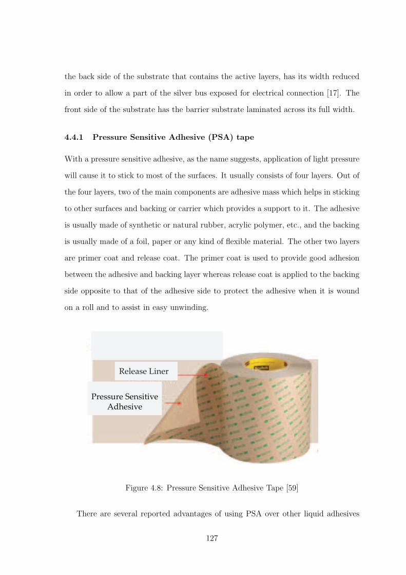
the back side of the substrate that contains the active layers, has its width reduced
in order to allow a part of the silver bus exposed for electrical connection [17]. The
front side of the substrate has the barrier substrate laminated across its full width.
4.4.1 Pressure Sensitive Adhesive (PSA) tape
With a pressure sensitive adhesive, as the name suggests, application of light pressure
will cause it to stick to most of the surfaces. It usually consists of four layers. Out of
the four layers, two of the main components are adhesive mass which helps in sticking
to other surfaces and backing or carrier which provides a support to it. The adhesive
is usually made of synthetic or natural rubber, acrylic polymer, etc., and the backing
is usually made of a foil, paper or any kind of flexible material. The other two layers
are primer coat and release coat. The primer coat is used to provide good adhesion
between the adhesive and backing layer whereas release coat is applied to the backing
side opposite to that of the adhesive side to protect the adhesive when it is wound
on a roll and to assist in easy unwinding.
Release Liner
Pressure SensitiveAdhesive
Figure 4.8: Pressure Sensitive Adhesive Tape [59]
There are several reported advantages of using PSA over other liquid adhesives
127
and fasteners.
• Along with the primary function of bonding of two materials, they help in
dampening vibration and shock, noise reduction and also help in obtaining a
highly effective sealing.
• As they do not require any drilling or welding such as mechanical fasteners, it
results in a smooth surface finish.
• PSAs eliminate the galvanic corrosion which can occur when two dissimilar
metallic materials are bonded and exposed to moisture.
• They avoid formation of concentrated stress areas by distributing the stress
uniformly over the bonded area.
• They also allow lamination of thinner substrates and materials with different
coefficients of thermal expansion.
Sometimes, an adhesive tape is made of just a release liner and an adhesive tape.
A release liner is a web of thin material which is used to cover the adhesive side of a
PSA to protect it during storage and transport as well as to provide support during
manufacturing and conversion. It is very important to choose a suitable release liner
as it will lead to an expensive process downtime if the liner material fails to protect
the adhesive material or releases prematurely. Thus, release liners must be reliable.
The release liners are made of suitable thin substrates with release coatings which
allow for easy delamination from the adhesive layer when needed. Release liner mate-
rial should be such that it should allow easy delamination from the adhesive without
scraping any adhesive part and also provide the necessary support for the adhesive
during its storage and transportation. Silicon coated release liners are very popular
in the industry as it requires less release forces than other materials. Lower nip pres-
sure is preferred for softer adhesives and fragile substrates whereas higher pressure is
128
preferred for firm adhesives and substrates. Usually, softer material such as rubber
or elastomer is preferred for the top nip roller while steel or hard rubber is preferred
for the bottom nip roller. The bottom roller may be nickel or chromium plated to
avoid corrosion and cuts and to be easy to clean.
4.4.2 Barrier Material
The barrier film made of silicon oxide coatings provide very good barrier properties;
Dupont company has barrier material made of silicon coatings deposited on their
Teonex Q65FA substrate. The silicon dioxide on Teonex Q65FA barrier material has
a density of 2.52 g/cm3 [60] and Teonex Q65FA has an elastic modulus of 5 GPa at
room temperature. The silicon coated PEN material has better barrier properties
than the silicon coated PET material [61]. Also, biaxially stretched PEN material is
superior in mechanical, thermal and gas barrier properties than biaxially stretched
PET material.
The thickness of silicon dioxide deposited on the film is about 90−120 nm. Teonex
Q65FA has an ultimate tensile strength 220 MPa and thickness of the film can be
around 100 micron. As the thickness of the barrier film increases, its flexibility de-
creases. So, it is better to keep the thickness of the film at minimum. As the thickness
of silicon coating on the Teonex film is minimal, it does not provide much stiffness.
Thus, in order to calculate the tension to run this web, the ultimate tensile strength
of Teonex film is considered.
4.4.3 Lamination of Barrier Material to Adhesive Layer
Before the lamination of barrier material to the solar cell substrate, an adhesive
layer must be laminated to the barrier material which is shown in Figure 4.9. The
adhesive material is protected by the liner material during the entire process. The
liner material is made in such a way that the adhesive does not stick to the inner layers
129
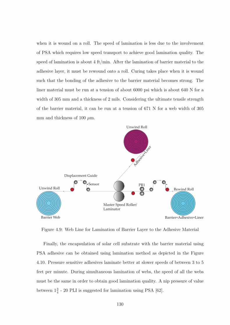
when it is wound on a roll. The speed of lamination is less due to the involvement
of PSA which requires low speed transport to achieve good lamination quality. The
speed of lamination is about 4 ft/min. After the lamination of barrier material to the
adhesive layer, it must be rewound onto a roll. Curing takes place when it is wound
such that the bonding of the adhesive to the barrier material becomes strong. The
liner material must be run at a tension of about 6000 psi which is about 640 N for a
width of 305 mm and a thickness of 2 mils. Considering the ultimate tensile strength
of the barrier material, it can be run at a tension of 671 N for a web width of 305
mm and thickness of 100 µm.
Unwind Roll
Rewind Roll
Master Speed Roller/Laminator
PR1
Adhe
sive
+Lin
er
Displacement Guide
Unwind Roll
Barrier Web Barrier+Adhesive+Liner
Sensor
Figure 4.9: Web Line for Lamination of Barrier Layer to the Adhesive Material
Finally, the encapsulation of solar cell substrate with the barrier material using
PSA adhesive can be obtained using lamination method as depicted in the Figure
4.10. Pressure sensitive adhesives laminate better at slower speeds of between 3 to 5
feet per minute. During simultaneous lamination of webs, the speed of all the webs
must be the same in order to obtain good lamination quality. A nip pressure of value
between 134- 20 PLI is suggested for lamination using PSA [62].
130
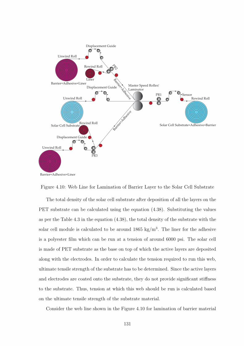
Unwind Roll
Displacement Guide
PR2
Rewind Roll
Unwind Roll
Displacement Guide
PR3
PR1
Displacement Guide
Unwind Roll
Rewind Roll
Rewind Roll
Master Speed Roller/Laminator
Barrier+Adhesive+Liner
Barrier+Adhesive+Liner
Solar Cell Substrate Solar Cell Substrate+Adhesive+Barrier
Liner
Barri
er+A
dhesiv
eBarrier+A
dhesive
Sensor
Figure 4.10: Web Line for Lamination of Barrier Layer to the Solar Cell Substrate
The total density of the solar cell substrate after deposition of all the layers on the
PET substrate can be calculated using the equation (4.38). Substituting the values
as per the Table 4.3 in the equation (4.38), the total density of the substrate with the
solar cell module is calculated to be around 1865 kg/m3. The liner for the adhesive
is a polyester film which can be run at a tension of around 6000 psi. The solar cell
is made of PET substrate as the base on top of which the active layers are deposited
along with the electrodes. In order to calculate the tension required to run this web,
ultimate tensile strength of the substrate has to be determined. Since the active layers
and electrodes are coated onto the substrate, they do not provide significant stiffness
to the substrate. Thus, tension at which this web should be run is calculated based
on the ultimate tensile strength of the substrate material.
Consider the web line shown in the Figure 4.10 for lamination of barrier material
131
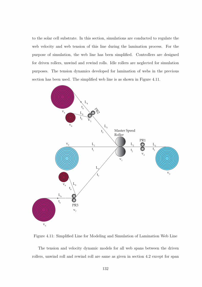
to the solar cell substrate. In this section, simulations are conducted to regulate the
web velocity and web tension of this line during the lamination process. For the
purpose of simulation, the web line has been simplified. Controllers are designed
for driven rollers, unwind and rewind rolls. Idle rollers are neglected for simulation
purposes. The tension dynamics developed for lamination of webs in the previous
section has been used. The simplified web line is as shown in Figure 4.11.
PR2
PR1
Master Speed Roller
PR3
v0
v1
v2
v3
V5
v6
v7
v8
v9
L1
t1
L9
L8
L7
L6
L5
L4
L3
L2
t9
t8
t7
t6
t5
t4
t3t
2
v4
Figure 4.11: Simplified Line for Modeling and Simulation of Lamination Web Line
The tension and velocity dynamic models for all web spans between the driven
rollers, unwind roll and rewind roll are same as given in section 4.2 except for span
132
L8 which is the span after the lamination of the three webs. The tension dynamic
equation for that particular span is obtained according to the equation (4.55).
The barrier material is laminated on both sides of the solar cell substrate for
encapsulation. However, the width of the solar cell substrate is about 305 mm and
width of the barrier substrate for lamination to the back side of the substrate is about
250 mm whereas front side of the substrate has the lamination to its entire width.
This is to allow the silver bus bars in the back side of the substrate to be exposed for
electrical connection during later stages.
4.5 Calculation of Reference Tension
For a web width of 305 mm, the PET substrate must be run at a tension of around
218 N. Since the liner material is already laminated to the barrier material, it has
to be run at a tension value which is the sum of the tensions required to run those
two web materials individually; although this is what is reported in literature, further
study must be conducted to verify this aspect. For the liner material of width 250
mm and thickness 2 mils, a tension value of 525 N is required. For the liner material
of width 305 mm and thickness 2 mils, a tension of around 640 N is required. For
a web width of 305 mm and thickness of 100 micron, tension required to run the
barrier material is about 671 N whereas for a web width of 250 mm, reference tension
of about 550 N is required.
Since the liner material with the barrier substrate is of reduced width on the back
side compared to the solar cell substrate, the tension dynamic equation (4.55) which
is derived should be modified to include the changes in the widths of the webs. The
lamination line includes simultaneous lamination of three webs i.e., barrier substrates
with adhesive laminated on either sides of the solar cell substrate. Thus, the tension
dynamic equation for this particular case involving lamination of three webs having
different widths is given as
133
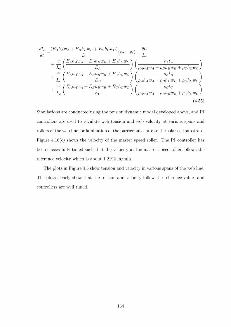
dtcdt
=(EAhAwA + EBhBwB + EChCwC)
Lc
(v2 − v1)−vtcLc
+v
Lc
(
EAhAwA + EBhBwB + EChCwC
EA
)(
ρAtAρAhAwA + ρBhBwB + ρChCwC
)
+v
Lc
(
EAhAwA + EBhBwB + EChCwC
EB
)(
ρBtBρAhAwA + ρBhBwB + ρChCwC
)
+v
Lc
(
EAhAwA + EBhBwB + EChCwC
EC
)(
ρCtCρAhAwA + ρBhBwB + ρChCwC
)
(4.55)
Simulations are conducted using the tension dynamic model developed above, and PI
controllers are used to regulate web tension and web velocity at various spans and
rollers of the web line for lamination of the barrier substrate to the solar cell substrate.
Figure 4.16(c) shows the velocity of the master speed roller. The PI controller has
been successfully tuned such that the velocity at the master speed roller follows the
reference velocity which is about 1.2192 m/min.
The plots in Figure 4.5 show tension and velocity in various spans of the web line.
The plots clearly show that the tension and velocity follow the reference values and
controllers are well tuned.
134
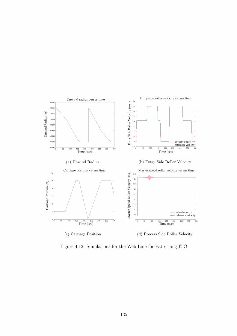
0 50 100 150 200 250 300 350 4000.1647
0.1648
0.1649
0.1649
0.1649
0.165
0.165
0.1651
0.1651
Unwind radius versus time
Un
win
d R
adiu
s (m
)
Time (sec)
(a) Unwind Radius
0 50 100 150 200 250 300 350 400−0.1
0
0.1
0.2
0.3
0.4
0.5
0.6
0.7
0.8
Entry side roller velocity versus time
------ actual velocity
------ reference velocityEn
try
Sid
e R
oll
er V
elo
city
(m
s-1)
Time (sec)
(b) Entry Side Roller Velocity
0 50 100 150 200 250 300 350 4000
5
10
15
20
25
30
Carriage position versus time
Car
riag
e P
osi
tio
n (
m)
Time (sec)
(c) Carriage Position
0 50 100 150 200 250 300 350 4000
0.05
0.1
0.15
0.2
0.25
0.3
0.35
0.4
0.45
------ actual velocity
------ reference velocity
Time (sec)
Master speed roller velocity versus time
Mas
ter
Sp
eed
Ro
ller
Vel
oci
ty (
ms-1
)
(d) Process Side Roller Velocity
Figure 4.12: Simulations for the Web Line for Patterning ITO
135
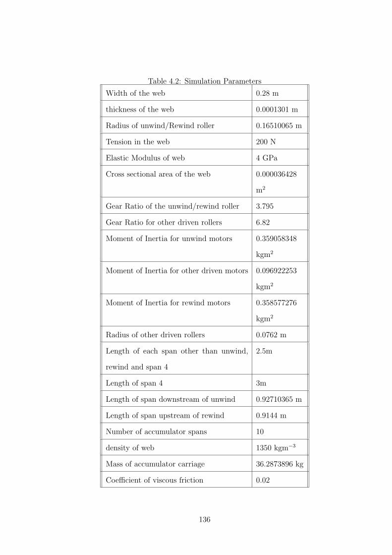
Table 4.2: Simulation Parameters
Width of the web 0.28 m
thickness of the web 0.0001301 m
Radius of unwind/Rewind roller 0.16510065 m
Tension in the web 200 N
Elastic Modulus of web 4 GPa
Cross sectional area of the web 0.000036428
m2
Gear Ratio of the unwind/rewind roller 3.795
Gear Ratio for other driven rollers 6.82
Moment of Inertia for unwind motors 0.359058348
kgm2
Moment of Inertia for other driven motors 0.096922253
kgm2
Moment of Inertia for rewind motors 0.358577276
kgm2
Radius of other driven rollers 0.0762 m
Length of each span other than unwind,
rewind and span 4
2.5m
Length of span 4 3m
Length of span downstream of unwind 0.92710365 m
Length of span upstream of rewind 0.9144 m
Number of accumulator spans 10
density of web 1350 kgm−3
Mass of accumulator carriage 36.2873896 kg
Coefficient of viscous friction 0.02
136
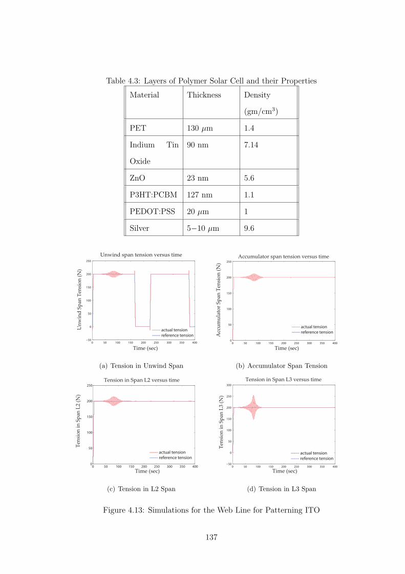
Table 4.3: Layers of Polymer Solar Cell and their Properties
Material Thickness Density
(gm/cm3)
PET 130 µm 1.4
Indium Tin
Oxide
90 nm 7.14
ZnO 23 nm 5.6
P3HT:PCBM 127 nm 1.1
PEDOT:PSS 20 µm 1
Silver 5−10 µm 9.6
0 50 100 150 200 250 300 350 400−50
0
50
100
150
200
250
Unwind span tension versus time
Un
win
d S
pan
Ten
sio
n (
N)
Time (sec)
------ actual tension
------ reference tension
(a) Tension in Unwind Span
0 50 100 150 200 250 300 350 4000
50
100
150
200
250
Accumulator span tension versus time
Acc
um
ula
tor
Sp
an T
ensi
on
(N
)
Time (sec)
------ actual tension
------ reference tension
(b) Accumulator Span Tension
0 50 100 150 200 250 300 350 4000
50
100
150
200
250
Tension in Span L2 versus time
Ten
sio
n i
n S
pan
L2
(N)
------ actual tension
------ reference tension
Time (sec)
(c) Tension in L2 Span
0 50 100 150 200 250 300 350 400−50
0
50
100
150
200
250
300
Tension in Span L3 versus time
Ten
sio
n i
n S
pan
L3
(N)
Time (sec)
------ actual tension
------ reference tension
(d) Tension in L3 Span
Figure 4.13: Simulations for the Web Line for Patterning ITO
137
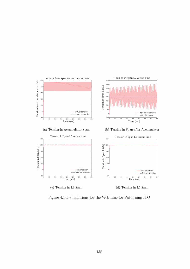
0 50 100 150 200 250 300 350 400−50
0
50
100
150
200
250
Accumulator span tension versus time
Ten
sio
n i
n a
ccu
mu
lato
r sp
an (
N)
Time (sec)
------ actual tension
------ reference tension
(a) Tension in Accumulator Span
0 50 100 150 200 250 300 350 400−50
0
50
100
150
200
250
300
350
400
Tension in Span L2 versus time
Ten
sio
n i
n S
pan
L2
(N)
Time (sec)
------ reference tension
------ actual tension
(b) Tension in Span after Accumulator
0 50 100 150 200 250 300 350 400−50
0
50
100
150
200
250
Tension in Span L3 versus time
Ten
sio
n i
n S
pan
L3
(N)
Time (sec)
------ actual tension
------ reference tension
(c) Tension in L3 Span
0 50 100 150 200 250 300 350 400−50
0
50
100
150
200
250
Tension in Span L5 versus time
------ actual tension
------ reference tension
Ten
sio
n i
n S
pan
L5
(N)
Time (sec)
(d) Tension in L5 Span
Figure 4.14: Simulations for the Web Line for Patterning ITO
138
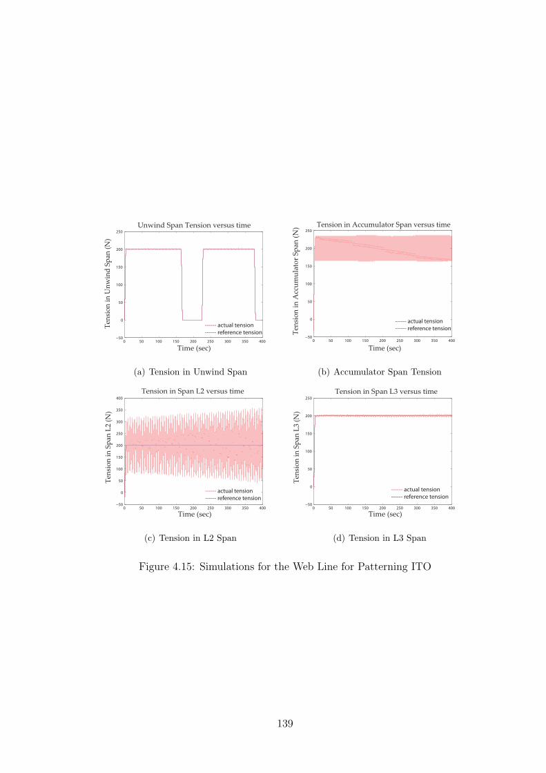
0 50 100 150 200 250 300 350 400−50
0
50
100
150
200
250
Unwind Span Tension versus time
Time (sec)
------ actual tension
------ reference tension
Ten
sio
n i
n U
nw
ind
Sp
an (
N)
(a) Tension in Unwind Span
0 50 100 150 200 250 300 350 400−50
0
50
100
150
200
250
Tension in Accumulator Span versus time
Ten
sio
n i
n A
ccu
mu
lato
r S
pan
(N
)
Time (sec)
------ actual tension
------ reference tension
(b) Accumulator Span Tension
0 50 100 150 200 250 300 350 400−50
0
50
100
150
200
250
300
350
400
Tension in Span L2 versus time
Ten
sio
n i
n S
pan
L2
(N)
Time (sec)
------ actual tension
------ reference tension
(c) Tension in L2 Span
0 50 100 150 200 250 300 350 400−50
0
50
100
150
200
250
Tension in Span L3 versus time
Ten
sio
n i
n S
pan
L3
(N)
Time (sec)
------ actual tension
------ reference tension
(d) Tension in L3 Span
Figure 4.15: Simulations for the Web Line for Patterning ITO
139
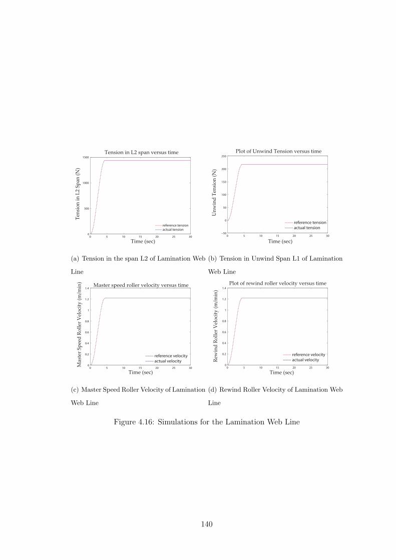
0 5 10 15 20 25 300
500
1000
1500
Tension in L2 span versus time
Ten
sio
n i
n L
2 S
pan
(N
)
Time (sec)
------ reference tension
------ actual tension
(a) Tension in the span L2 of Lamination Web
Line
0 5 10 15 20 25 30−50
0
50
100
150
200
250
Time (sec)
Un
win
d T
ensi
on
(N
)
Plot of Unwind Tension versus time
------ reference tension
------ actual tension
(b) Tension in Unwind Span L1 of Lamination
Web Line
0 5 10 15 20 25 300
0.2
0.4
0.6
0.8
1
1.2
1.4
Time (sec)
Mas
ter
Sp
eed
Ro
ller
Vel
oci
ty (
m/m
in)
Master speed roller velocity versus time
------ reference velocity
------ actual velocity
(c) Master Speed Roller Velocity of Lamination
Web Line
0 5 10 15 20 25 300
0.2
0.4
0.6
0.8
1
1.2
1.4
Time (sec)
Plot of rewind roller velocity versus time
Rew
ind
Ro
ller
Vel
oci
ty (
m/m
in)
------ reference velocity
------ actual velocity
(d) Rewind Roller Velocity of Lamination Web
Line
Figure 4.16: Simulations for the Lamination Web Line
140
CHAPTER 5
Summary and Future Work
5.1 Summary
Flexible electronics may be bent, flexed and rolled to an extent and still be expected
to maintain their functionality. The components of flexible electronic devices can be
printed using solution printing technologies such that the entire manufacturing can be
done using RTR manufacturing. The main focus of this thesis was on manufacturing
of flexible electronics using RTR methods. Based on a comprehensive study of the
various processes involved in manufacturing of flexible electronic devices, OLEDs
and polymer solar cells in particular, web handling strategies and parameters were
determined for continuous processing of flexible electronic devices using several web
lines. It is important to regulate web tension and velocity during its transport from
the unwind roll to the rewind roll. In this thesis, simulations were conducted for
the web lines for regulating web tension and velocity. Lamination of webs is a very
important process, especially in flexible electronics manufacturing. This is because
the barrier layer must be laminated to the flexible electronic substrate on both sides of
it to prevent it from being degraded by the environmental permeates such as oxygen
and moisture. In this thesis, a web line for simultaneous lamination of barrier material
to both sides of the substrate was designed. A chapter by chapter summary is given
below.
Chapter 2 provided detailed discussions about two of the main flexible electronic
devices, OLEDs and polymer solar cells. The first section of this chapter provided
details about OLEDs; insights into various parts of OLED, their functions, deposition
141
methods, advantages and disadvantages of OLEDs, etc., was given. A discussion on
different OLED types and insights into the manufacture of flexible OLEDs was given.
The second section provided insights into polymer solar cells, its components and
functionalities. In the last part of this chapter, the manner in which polymer solar
cell can be used to charge a battery to light a solar lamp was presented.
In chapter 3, a web line was designed for RTR patterning of ITO anode layer on
the PET substrate. Various process parameters and technologies are determined for
the ITO patterning in the web line. Solution printing technologies and various web
handling techniques were discussed such that ITO patterning can be performed in
a continuous manner. Web line parameters such as web tension and velocity were
determined for the web line. In the second part of this chapter, a web line for the
deposition of active layers on the anode layer of the plastic substrate was designed
and discussed. The manner in which the web can be passed through liquid baths
was discussed. In the last part of this chapter, the manner in which the longitudinal
registration between two successive printing units can be obtained using compensator
rollers was presented.
In chapter 4, drag force on the web as it passes through a liquid bath was calcu-
lated. Laminar flow for the fluid in the bath in the crosswise direction to the web
movement is considered for drag force calculation. Tension and velocity dynamic
models for various web spans, accumulators and rollers of the web line for patterning
of ITO anode were presented. Simulations were conducted to regulate tension and
velocity of the web using the tension and velocity dynamic models. Modeling of the
tension dynamics for lamination of two webs was discussed. A barrier material that
protects the polymer solar cell against oxygen and moisture was identified. A web line
was designed for the lamination of barrier material to the pressure sensitive adhesive.
A web line was also designed for simultaneous lamination of barrier material onto
both sides of the flexible electronic substrate. Web line parameters and lamination
142
conditions were determined for the web lines designed for lamination. Using the ten-
sion dynamic model developed for lamination of webs, simulations were conducted
to regulate web tension and velocity for lamination of barrier material to the flexible
electronic substrate.
5.2 Future Work
Web lines designed in this thesis can be modified to manufacture other flexible elec-
tronic devices using RTR methods. The designed web lines must be modified to
manufacture other flexible electronic devices. As the manufacturing of electronic de-
vices requires high precision, registration in the lateral direction is necessary along
with longitudinal registration. Thus, proper methods must be developed for obtaining
accurate registration in the lateral direction of the web movement. Future research
should focus on optimizing the process and web line parameters for the designed web
lines for the manufacturing of flexible electronic devices. Research must be conducted
on the materials such that only solution printing technologies could be used for de-
position of all the components of flexible electronic devices. For example, the ITO
anode material on the substrate is not deposited by solution printing technology, only
the patterning is done using RTR method. So, research must be conducted on se-
lection of materials that would replace the ITO as the anode material which can be
deposited by solution printing techniques. The drag force calculation was done for
the laminar flow of the fluid in the bath. It was determined that the laminar flow
of fluid does not result in a drag force that is significant. However, the flow may
not be laminar in many situations, and drag force may not be insignificant in such
situations. Therefore, further study on this aspect must be conducted.
Research must be focused on technologies that would assist in increasing web
speed and yet obtaining a good quality product. The lamination tension dynamic
model was developed using rule of mixture considering the web to be isotropic; both
143
these assumptions weakly reflect practical situations. Research should be done on
developing tension dynamic model for simultaneous lamination of non-isotropic ma-
terial webs. Research must be conducted on finding better barrier materials for the
encapsulation of flexible electronic devices. Future work must focus on finding elec-
trode materials for the flexible electronics which do not get oxidized in air eliminating
the need for an inert atmosphere during their deposition. The presence of an inert
atmosphere poses problems during RTR manufacturing and also increases the cost.
Finally, several test web platforms must be developed to conduct experimentation
which will help validate the proposed designs, and also help in making improvements
to the proposed techniques.
144
BIBLIOGRAPHY
[1] J. Vilches, “Hp unveils flexible display prototype.” Internet: http://www.
techspot.com/news/32780-hp-unveils-flexible-display-prototype-.
html.
[2] Admin, “Flexible next generation display screen from LG philips.” Internet:
http://www.sexygadgets.net/2009/08/27/flexible-next-generation-di.
.splay-screen-from-lg-philips/.
[3] Admin, “Oleds from samsung, epson and cmel at fpd-international in yoko-
hama.” Internet: http://www.oled-display.info/oled/samsung.
[4] Deepa, “Flexible solar panels rolled out by powerfilm.” Internet:
http://www.ecofriend.com/entry/flexible-solar-panels-rolled-out-.
.by-powerfilm/.
[5] D. Kaplan, “The arrival of flexible chips a summary.” Internet:
http://venturebeat.com/2007/06/22/the-arrival-of-flexible-chips-.
.a-summary/.
[6] G. Crawford, Flexible Flat Panel Displays. Wiley Series in Display Technology,
1st ed., 2005.
[7] B. Media, “Inspired by nature, a better artificial muscle was de-
veloped.” Internet: http://www.homelyscientist.com/2007/07/inspired.
.-by-nature-a-better-artificial-muscle-was-developed/.
145
[8] Admin, “What is an oled display.” Internet: http://ledtvsforsale.com/
what-is-an-oled-display/.
[9] C. Freudenrich, “How oleds work.” Internet: http://electronics.
howstuffworks.com/oled2.htm.
[10] B. Geffroy, P. Roy, and C. Prat, “Oled technology: materials, devices and display
technologies,” Polymer International, 2006.
[11] K. Jain, M. Klosner, M. Zemel, and S. Raghunandan, “Flexible electronics
and displays: High-resolution, roll-to-roll, projection lithography and photoab-
lation processing technologies for high-throughput production,” Proceedings of
the IEEE, vol. 93, pp. 1500–1510, Aug. 2005.
[12] C. Freudenrich, “How oleds work.” Internet:http://electronics.
howstuffworks.com/oled3.htm.
[13] M. C. Choia, Y. Kimb, and C. S. Ha, “Polymers for flexible displays: From ma-
terial selection to device applications,” Journal of Progress in Polymer Science,
vol. 33, pp. 581–630, Jun. 2008.
[14] K. P. Homer Antoniadis, “Organic light emitting diode light source,” U.S.
Patent 7319440, Jan 2008.
[15] W. J. Nam, “Electroluminiscent display,” U.S. Patent 2008/0012485, Jan 2008.
[16] Y.-R. SONG, K.-T. PARK, and B.-R. CHOI, “Organic light emitting diode
display and method of manufacturing the same,” U.S. Patent 2008/0042549,
Feb 2008.
[17] F. C. Krebs, T. Tromholt, and M. Jørgensen, “Upscaling of polymer solar cell
fabrication using full roll-to-roll processing,” Nanoscale, Feb. 2010.
146
[18] VTT, Acreo, and TNO, “Manufacturing and Production Equipment and Sys-
tems for Polymer and Printed Electronics,” EUROPEAN COMMISSION, Feb.
2010.
[19] F. C. Krebs, J. Fyenbo, and M. Jørgensen, “Product integration of compact roll-
to-roll processed polymer solar cell modules: methods and manufacture using
flexographic printing, slot-die coating and rotary screen printing,” Journal of
Materials Chemistry, vol. 20, pp. 8994–9001, May 2010.
[20] Coatema, “Rotary screen system.” Internet: http://www.coatema.de/eng/
lab_solutions/modular_coating/rotary_screen_system.php.
[21] J. M. Brethour, “Coating with deformable and permeable surfaces: Focus on
rotary screen coating,” PhD thesis, Apr. 2003.
[22] M. Mitter, “Arrangement for preventing screen deformation,” U.S. Patent
4497249, Feb. 1985.
[23] C. design, “Gravure printing.” Internet: http://www.cncdesign.com.au/
productionmachine/printing01.html.
[24] K. Hopcus, “What type of web guide you need.” Internet: http://maxcessu.
com/files/Fife_Guide_Selection.pdf.
[25] P. Eggen, “Get a grip on your web.” Internet: http://pffc-online.com/web_
handling/tension/paper-grip-on-web-1109/.
[26] T. Walker, “Tensioning webs: Tension feedback.” Internet: http://www.
webhandling.com/TensionFeedback.
[27] K. Yamashita, T. Itashiki, T. Motomura, K. Minami, and I. Sawada, “Rotary
cooling roller,” U.S. Patent 6675876, Jan. 2004.
147
[28] P. R. Pagilla, A. Seshadri, and J. Lynch, “Modeling and analysis of rotogravure
printing presses,” Proceedings Of The Eleventh International Conference On
Web Handling, Jun. 2011.
[29] Globalspec, “Transfer adhesive tapes datasheets.” Internet: http://www.
globalspec.com/ds/4289/areaspec/application_transfer.
[30] P. Nath and M. Izu, “Performance of large area amorphous si based single and
multiple junction solar cells,” Institute of Electrical and Electronic Engineers,
pp. 939–942, Oct. 1985.
[31] M. Yano, K. Suzuki, K. Nakatani, and H. Okaniwa, “Roll-to-roll preparation of
a hydrogenated amorphous silicon solar cell on a polymer film substrate,” Thin
Solid Films, vol. 146, pp. 75–81, 1987.
[32] P. Smith, P. Carey, and T. Sigmon, “Excimer laser crystallization and doping
of silicon films on plastic substrates,” American Institute of Physics, Jan. 1997.
[33] N. Young, G. Harkin, R. Bunn, D. McCulloch, R. Wilks, and A. Knapp, “Novel
fingerprint scanning arrays using polysilicon tft’s on glass and polymer sub-
strates,” IEEE Electron Device Letters, vol. 18, Jan. 1997.
[34] J. Liu, L. N. Lewis, A. R. Duggal, and T. J. Faircloth, “High performance
organic light-emitting diodes fabricated via a vacuum-free lamination process,”
Journal of Applied Physics Letters, vol. 88, pp. 223509 1–223509 3, Jun. 2006.
[35] H. H. Yu, S. J. Hwang, and K. C. Hwang, “Preparation and characterization of
a novel flexible substrate for oled,” Opt. Commun, vol. 248, p. 51, 2005.
[36] L. Hui, Y. Junsheng, W. Nana, H. Chunhua, and J. Yadong, “Flexible organic
light-emitting diodes with improved performance by insertion of an UV-sensitive
148
layer,” Journal of Vacuum Science and Technology, vol. 26, pp. 1379–1381, Jul.
2008.
[37] D. Li and L. J. Guo, “Organic thin film transistors and polymer light-emitting
diodes patterned by polymer inking and stamping,” Journal of Applied Physics
Letters, vol. 41, p. 105115, 2008.
[38] J. H. Kim, M. C. Choi, H. Kim, and Y. Kim, “Colorless polyamide/organoclay
nanocomposite substrates for flexible organic light-emitting devices,” Journal
of Nanoscience and Nanotechnology, vol. 87, pp. 552–563, May 2009.
[39] V. Finland, S. ACREO, T. N. TNO, G. TU Chemnitz, G. Fraunhofer EMFT,
and B. IMEC, “Final vision document in roll-to-roll printed electronics manu-
facturing equipment, production lines and systems,” EUROPEAN COMMIS-
SION.
[40] F. C. Krebs, “Polymer solar cell modules prepared using roll-to-roll methods:
Knife-over-edge coating, slot-die coating and screen printing,” Solar Energy
Materials and Solar Cells, vol. 93, pp. 465–475, 2009.
[41] S. G. Wentink and S. D. Koch, “UV curing in screen printing for printed circuits
and the graphic arts,” Norwalk, Conn.: Technology Marketing Corp., 1981.
[42] V. Belluz, “In-line continuous forming of a coated plastic substrate,” U.S.
Patent 2010/0119831, May 2010.
[43] A. Challaye, “Device for guiding a strip in a liquid bath,” U.S. Patent 0064968,
Mar. 2010.
[44] H. Kipphan, Handbook of Print Media. Springer, 2001.
[45] Matweb, “Tensile property testing of plastics.” Internet: http://www.matweb.
com/reference/tensilestrength.aspx.
149
[46] T. Walker, “Web handling.” Internet: http://www.webhandling.com/WHMain,
2009.
[47] J. Greener, K. Ng, K. Vaeth, and T. Smith, “Moisture permeability through
multilayered barrier films as applied to flexible oled display,” Journal of Applied
Polymer Science, vol. 106, pp. 3534–3542, Dec. 2007.
[48] S. J. Bae, J. W. Lee, J. S. Park, D. Y. Kim, S. W. Hwang, J.-K. Kim, and B.-K.
Ju, “Enhancement of barrier properties using ultrathin hybrid passivation layer
for organic light emitting diodes,” Japanese Journal of Applied Physics, vol. 45,
no. 7, pp. 5970–5973, 2006.
[49] R. W. E. I. Corporation, “A Techonology Decision - Adhesive lamination or
extrusion coating/lamination,” TAPPI e-Library, 2010.
[50] P. Rath and J. C. Chai, “Modeling Convection-Driven Diffusion Controlled Wet
Chemical Etching Using A Total-Concentration Fixed-Grid Method,” Numer-
ical Heat Transfer, PART B, no. 53, pp. 143–159, 2008.
[51] D. G. Beckett, “Demetallizing procedure,” United States Patent 5340436, Aug.
1994.
[52] P. Weidman, “New solutions for laminar boundary layers with cross flow,” Z.
angew. Math. Phys., vol. 48, pp. 341–356, 1997.
[53] S. D. Kasten, H. W. Sam, and Rex, “Cucl etching.” Internet: http://www.
xertech.net/Tech/CuCl_ech.html.
[54] M. Laliberte, “Model for calculating the viscosity of aqueous solutions,” J.
Chem. Eng. Data, vol. 52, pp. 321–335, 2007.
[55] M. Laliberte and W. E. Cooper, “Model for calculating the density of aqueous
electrolyte solutions,” J. Chem. Eng. Data, vol. 49, pp. 1141–1151, 2004.
150
[56] R. V. Dwivedulla, “Modeling the effects of belt compliance, backlash, and slip
on web tension and new methods for decentralized control of web processing
lines,” PhD Thesis, Dec. 2005.
[57] P. R. Pagilla, I. Singh, and R. V. Dwivedulla, “A study on control of accumu-
lators in web processing lines,” American Control Conference, vol. 5, pp. 3684–
3689, Jun. 2003.
[58] P. R. Pagilla, K. Reid, and J. Newton, “Modeling of laminated webs,” Proceed-
ings Of The Ninth International Conference On Web Handling, JUN. 2007.
[59] F. Express, “A comprehensive guide to laminating.” Internet: http://www.
factory-express.com/buyers_guide/lamination_guide.html.
[60] W. MacDonald, K. Rollins, D. MacKerron, R. Eveson, R. Rustina, R. Adam,
K. Looney, K. Rakos, and K. Hashimoto, “Latest developments in polyester
film for flexible electronics.” Internet: http://people.ccmr.cornell.edu/
~cober/mse542/page2/files/Barriers.pdf.
[61] N. Inagaki, V. Cech, K. Narushima, and Y. Takechi, “Oxygen and water va-
por gas barrier poly(ethylene naphthalate) films by deposition of siox plasma
polymers from mixture of tetramethoxysilane and oxygen,” Journal of Applied
Polymer Science, vol. 104, pp. 915–925, 2007.
[62] M. Company, “High performance adhesive tapes with adhesive 200mp.” Inter-
net: http://multimedia.3m.com/mws/mediawebserver?66666UuZjcFSLXT.
.tlXTyLxfyEVuQEcuZgVs6EVs6E666666--Flexcon.
[63] D. R. Roisum, The Mechanics Of Web Handling. Tappi Press, 1st ed., 1998.
[64] W. H. R. Center, “An applications seminar on web handling,” Oklahoma State
University, Mar. 2002.
151
[65] W. H. R. Center, “An applications seminar on web handling,” Oklahoma State
University, Sep. 2005.
[66] K.-H. Kim, N.-M. Park, T.-Y. Kim, K. S. Cho, J. lk Lee, hye Yong Chu, and
G. Y. Sung, “Indium tin oxide films grown on polyethersulphone PES substrates
by pulsed-laser deposition PLD for use in organic light-emitting diodes,” ETRI
Journal, vol. 27, pp. 405–410, aug. 2005.
[67] G. Gustaffson, G. M. Treacy, Y. Cao, F. Klavertter, N. Colaneri, and A. J.
Heeger, “The ‘plastic’ led; a flexible light-emitting device using a polyaniline
transparent electrode,” Synth. Met., vol. 57, pp. 4123–4127, aug. 1993.
[68] D. Karnakis, A. Kearsley, and M. Knowles, “Ultrafast laser patterning of
oleds on flexible substrate for solid-state lighting,” Journal of Laser Mi-
cro/Nanoengineering, vol. 4, no. 3, 2009.
[69] S. W. Cho and et al., “Highly flexible, transparent, and low resistance indium
zinc oxide-ag-indium zinc oxide multi layer anode on polyethylene terephtha-
late substrate for flexible organic light-emitting diodes,” Journal of Thin Solid
Films, vol. 516, pp. 7881–7885, sep. 2008.
[70] J. M. Han, J. W. Han, J. Y. Chun, C. H. Ok, and D. S. Seo,
“Novel encapsulation method for flexible organic light-emitting diodes us-
ing poly(dimethylsiloxane),” Japanese Journal of Applied Physics, vol. 47,
pp. 8986–8988, sep. 2008.
[71] Y. S. Tsai, S. H. Wang, , and S. L. Chen, “Performance improvement of flexible
organic light-emitting diodes with double hole transport layers by spin-coating
and evaporation,” Japanese Journal of Applied Physics, vol. 48, no. 5, p. 052103,
2009.
152
[72] Y. H. Cheng, C. M. Chen, C. H. Cheng, and M. C. M. Lee, “Demonstra-
tion of organic light emitting diodes fabricated on flexible al2o3-embedded
poly(dimenthylsiloxane) substrates,” Japanese Journal of Applied Physics,
vol. 48, no. 5, p. 021502, 2009.
[73] S. Ie, J. H. Kim, B. T. Bae, dong Hee Park, J. W. Choi, and W. K. Choi,
“Amorphous indium tin oxide electrodes for piezoelectric and light-emitting
device deposited by vacuum roll to roll process,” Journal of Thin Solid Films,
vol. 517, pp. 4015–4018, May 2009.
[74] A. Maaninen, “Printed oleds,” Printed Intelligence Research at VTT, pp. 10–13,
2010.
[75] F. C. Krebs, “Fabrication and processing of polymer solar cells: A review
of printing and coating techniques,” Solar Energy Materials and Solar Cells,
vol. 93, pp. 394–412, Oct. 2008.
[76] A. Maaninen, M. Tuomikoski, M. Vlimki, and T. Maaninen, “All printed flexible
oleds,” Research and development activities in printed intelligence, pp. 14–16,
Oct. 2008.
[77] K. Jain, M. Klosner, M. Zemel, and S. Raghunandan, “Flexible electronics and
displays: High resolution, R2R, Projection Lithography and Photo ablation
Processing Technologies for High-Throughput Production,” IEEE Proceedings,
vol. 93, pp. 1500–1510, Oct. 2005.
[78] T. H. Tsa and Y. F. Wu, “Wet etching mechanisms of ito films in oxalic acid,”
Microelectronic Engineering, vol. 83, pp. 536–541, Aug. 2006.
[79] S. Sahasithiwat, L. Menbangpung, S. Aukkaravittayapan, and C. T. yanont,
“Fabrication of polymer solar cells at MTEC,” National Metal and Materials
Technology Center.
153
[80] R. Lynch, “Web handling seminar,” Oklahoma State University Web Handling
Research Center, Oct 2010.
[81] L. M. Lai, “Method of demetallizing a web in an etchant bath and web suitable
therefor,” U.S. Patent 6645389, Nov. 2003.
[82] N. Espinosa, R. G. Valverde, A. Urbina, and F. C. Krebs, “A life cycle analysis
of polymer solar cell modules prepared using roll-to-roll methods under ambient
conditions,” Solar Energy Materials and Solar Cells, Jun. 2010.
[83] D. G. Beckett, “Demetallizing procedure,” U.S. Patent 5628921, May. 1997.
[84] M. A. Robkin and C. R. Porter, “Control of hole size in filters by measuring
the amount of radiation passing through holes and correspondingly controlling
speed of filter moving through etching bath,” U.S. Patent 3585395, Jun. 1971.
[85] Z. Chen, E. Wiedemann, and Q. Liu, “Wet etching of zinc tin oxide thin films,”
U.S. Patent 2009/0075421, Mar. 2009.
[86] J. D. McCann and D. F. Tunmore, “Printer architecture,” U.S. Patent 6003988,
Dec. 1999.
[87] M. E. Kamen and M. Wells, “Apparatus and method for direct rotary screen
printing radiation curable compositions onto cylindrical articles,” U.S. Patent
6601502, aug. 2003.
[88] K. Budinski, “Friction of plastic webs,” Tribology International, vol. 34, pp. 625–
633, aug. 2001.
[89] Derks, Marius, and Joseph, “Rotary screen printing machine,” European Patent
0879145, Jan. 2000.
[90] J. G. Victor, M. Wilkinson, and S. Carter, “Screen printing light-emitting poly-
mer patterned devices,” U.S. Patent 6605483, aug. 2003.
154
[91] P. F. Cote, “Method of forming a patterned aluminium layer and article,” U.S.
Patent 4869778, Sep. 1989.
[92] A. Stagnaro, “Design and development of a roll-to-roll machine for continuous
high-speed microcontact printing,” M.S. thesis, Aug. 2008.
[93] P. E. Burrows, G. Gu, V. Bulovic, Z. Shen, S. R. Forrest, and M. E. Thompson,
“Achieving full-color organic light-emitting devices for lightweight, flat-panel
displays,” IEEE Transactions On Electron Devices, vol. 44, Aug. 1997.
[94] P. E. Burrows and et al., “Ultra barrier flexible substrates for flat panel dis-
plays,” Displays, vol. 22, pp. 65–69, Aug. 2001.
[95] A. G. Erlat, M. Yan, and A. R. Duggal, “Substrates and thin-film barrier
technology for flexible electronics,” Flexible Electronics, Electronic Materials:
Science and amp; Technology, vol. 11, p. 413, 2009.
[96] M. K. Han, “Am backplane for amoled,” School of Electric Engineering and
Computer Science.
[97] R. Hattori and C. H. Shim, “Full hd amoled current-programmed driving with
negative capacitance circuit technology,” Dept. of Electronics, Kyushu Univer-
sity, Motooka.
[98] F. C. Krebs and et al., “A complete process for production of flexible large area
polymer solar cells entirely using screen printingfirst public demonstration,”
Solar Energy Materials and SolarCells, vol. 93, pp. 422–441, 2009.
[99] K. DeRegge and J. Huwaert, “UV curing structure and process,” U.S. Patent
7704564, Apr. 2010.
[100] H. Jin, “Novel patterning methods for full-color polymer light-emitting dis-
plays,” PhD thesis, Jan. 2010.
155
[101] F. Krebs and et al., “A round robin study of flexible large-area roll-to-roll
processed polymer solar cell modules,” Sol. Energy Mater.Sol. Cells, vol. 93,
pp. 1968–1977, Jul. 2009.
[102] C. DeBoer, “Oled technology: Also am oled, pm oled, sm oled, pled and lep.”
Internet: www.audioholics.com/education/display-formats-technology/
display-technologies-guide-lcd-plasma-dlp-lcos-d-ila-crt/
display-technologies-guide-lcd-plasma-dlp-lcos-d-ila-crt-page-9,
August 2004.
[103] C. Freudenrich, “How OLEDs Work.” Internet: http://electronics.
howstuffworks.com/oled2.htm, 1998.
[104] B. Science, “Spin coater theory.” Internet: http://www.brewerscience.
com/products/cee-benchtop-products/cee-technical-information/
spin-coater-theory, 1997.
[105] Coatema, “Rotary screen system.” Internet: http://www.coatema.de/eng/
lab_solutions/modular_coating/rotary_screen_system.php.
[106] D. Mohankumar, “Organic LED. the exciting display device.” Internet:
http://electroschematics.com/5178/organic-led-the-exciting.
.-display-device/, February 2010.
[107] B. Stephens, “Screen Printing Squeegees: How to Pull Prints.” Internet:
http:..//www.signindustry.com/screen/articles/2004-07-29-BS-How.
.ToPullPrintswSqueegees.php3, 1999.
[108] J. I. Chemicals, “What is UV.” Internet: http://www.jaincouv.com/
more-about-uv.html, 2009.
156
[109] P. Company, “Recommended processing/handling procedures for norclad
copper clad laminates.” Internet: http://www.polyflon.com/Pdf/NORCLAD%
20Processing%20Guide.pdf, 1997.
[110] P. Chemistry, “The glass transition.” Internet: http://faculty.uscupstate.
edu/llever/Polymer%20Resources/GlassTrans.htm, July 2000.
[111] SOMATECH, “Pull rolls.” Internet: http://www.somatec-hameln.com/
_news/38.htm, August 2010.
[112] T. C. I. Incorporation, “Gravure coating.” Internet: http://www.tciinc.com/
coating.html.
[113] Y. Galagan, I. G. de Vries, A. P. Langen, R. Andriessen, W. J. Verhees, S. C.
Veenstra, and J. M. Kroon, “Technology development for roll to roll produc-
tion of organic photovoltaics,” Chemical Engineering and Processing: Process
Intensification, no. 50, pp. 454–461, 2011.
[114] M. A. Smith, N. M. M. Jones, S. L. Page, and M. P. Dirda, “Pressure-sensitive
tape and techniques for its removal from paper,” The American Institute for
Conservation, vol. 23, pp. 101–113, Feb. 1984.
[115] M. Sloboda, “The growing importance of release liners in pharmaceutical man-
ufacturing,” Pharmaceutical Technology Europe, vol. 23, Feb. 2011.
[116] A. Corporation, “Improving Production Efficiency with Optimal Release Lin
ers.” Internet: http://www.pddnet.com/product-improving-production-.
.efficiency.
[117] W. S. Wong and A. Sallero, Flexible electronics (electronic resource): materials
and applications. New York; London: Springer, 1st ed., 2008.
157
[118] R. Corporation, “Tips for cold lamination.” Internet: http://www.rtape.com/
resources/tips/tips-for-cold-laminations.
[119] D. T. Films, “Flexible electronics.” Internet: http://usa.dupontteijin.
.films.com/marketspaces/electricalcomponents/flexibleelectronics.
aspx.
[120] I. International Dielectric Products, “Physical-thermal properties.” In-
ternet: http://internationaldielectric.com/index.php?option=com_
content&view=article&id=5:mylar&catid=1:dupont&Itemid=3.
[121] Dupont, “Technical data teonex q65fa.” Internet: http://www.
teijindupontfilms.jp/english/pdf/teonex_q65fa.pdf.
[122] Z-MITETM , “Zinc Oxide Nanoparticle.” Internet: http://www.american.
.elements.com/Z-MITE%20PRODUCT%20INFORMATION.pdf.
[123] Z. Li, X. Zhang, and G. Lu, “Electron structure and dynamics at
poly(3−hexylthiophene)/fullerene photovoltaic heterojunctions,” APPLIED
PHYSICS LETTERS, vol. 98, Feb. 2011.
[124] SIGMA−ALDRICH, “Poly(3,4−ethylenedioxythiophene)−poly(styrenesulfonate).”
Internet: http://www.sigmaaldrich.com/catalog/ProductDetail.do?D7=
0&N5=SEARCH_CONCAT_PNO|BRAND_KEY&N4=560596|ALDRICH&N25=0&QS=ON&F=
SPEC.
[125] F. N. Stein, “The density of silver.” Internet: http://www.arps.org/users/
hs/palmers/ChemistryHonors/Unit0/Sample_Lab_Report.pdf.
158
VITA
Muthappa Ponjanda Madappa
Candidate for the Degree of
Master of Science
Thesis: ROLL TO ROLL MANUFACTURING OF FLEXIBLE ELECTRONIC DE-VICES
Major Field: Mechanical and Aerospace Engineering
Biographical:
Personal Data: Born in Coorg, India on February 7, 1985.
Education:Received the B.S. degree from Visveswaraya Technological University, In-dia, 2006, in Mechanical EngineeringCompleted the requirements for the degree of Master of Science with amajor in Mechanical and Aerospace Engineering at Oklahoma State Uni-versity in December, 2011.
Experience:Research Assistant at Oklahoma State University from May 2009 to De-cember 2011; Teaching Assistant at Oklahoma State University from Au-gust 2008 to May 2009; Software Engineer at Infosys Technologies Limitedfrom July 2006 to June 2008.
Name: MUTHAPPA PONJANDA MADAPPA Date of Degree: December, 2011
Institution: Oklahoma State University Location: Stillwater, Oklahoma
Title of Study: ROLL TO ROLL MANUFACTURING OF FLEXIBLE ELEC-TRONIC DEVICES
Pages in Study: 158 Candidate for the Degree of Master of Science
Major Field: Mechanical and Aerospace Engineering
Scope and Method of Study: Flexible electronics may be bent, flexed and rolled toan extent and still be expected to maintain their functionality. The focus of this the-sis is on efficient manufacture of electronic devices in flexible form using roll to roll(RTR) method of continuous manufacturing, which is expected to significantly im-prove productivity and efficiency and reduce manufacturing costs. A comprehensivestudy of the literature was undertaken to understand the various processes involved inthe manufacture of flexible electronics such as organic light emitting diodes (OLEDs)and solar cells, and an investigative study was carried out to highlight those processesand methods that are suitable for RTR manufacture of flexible electronic devices. De-sign of three web lines for RTR manufacturing of different stages of flexible electronicdevices was investigated.
Summary: Based on a comprehensive study of the various processes involved in man-ufacturing of flexible electronic devices, OLEDs and polymer solar cells in particular,web handling strategies and parameters were determined for continuous processing offlexible electronic devices using several web lines. The drag force on the web materialwas calculated based on the crosswise laminar movement of the fluid in the liquidbath through which the web is transported. Simulations were conducted to regulatetension and velocity of the web using the governing equations for web tension andvelocity. The web process lines designed in this thesis for OLEDs and solar cells canbe modified to manufacture other flexible electronic devices using RTR methods. Amodel for web tension for lamination of two webs was investigated. This model wasused for studying the tension behaviour during simultaneous lamination of barriermaterials to both sides of a solar cell substrate material.
ADVISOR’S APPROVAL:
Related Documents