1012 IEEE TRANSACTIONS ON INDUSTRIAL ELECTRONICS, VOL. 56, NO. 4, APRIL 2009 Robust Design of RF-MEMS Cantilever Switches Using Contact Physics Modeling Mohammed M. Shalaby, Zhongde Wang, Member, IEEE, Linda L.-W. Chow, Member, IEEE, Brian D. Jensen, John L. Volakis, Fellow, IEEE, Katsuo Kurabayashi, Member, IEEE, and Kazuhiro Saitou, Senior Member, IEEE Abstract—This paper presents the robust design optimization of an RF-MEMS direct contact cantilever switch for minimum ac- tuation voltage and opening time, and maximum power handling capability. The design variables are the length and thickness of the entire cantilever, the widths of the sections of the cantilever, and the dimple size. The actuation voltage is obtained using a 3-D structural-electrostatic finite-element method (FEM) model, and the opening time is obtained using the same FEM model and the experimental model of adhesion at the contact surfaces developed in our previous work. The model accounts for an unpredictable variance in the contact resistance resulting from the microma- chining process for the estimation of the power handling. This is achieved by taking the ratio of the root mean square power of the RF current (“signal”) passing through the switch to the contact temperature (“noise”) resulting from the possible range of the contact resistance. The resulting robust optimization problem is solved using a Strength Pareto Evolutionary Algorithm, to obtain design alternatives exhibiting different tradeoffs among the three objectives. The results show that there exists substantial room for improved designs of RF-MEMS direct-contact switches. It also provides a better understanding of the key factors contributing to the performances of RF-MEMS switches. Most importantly, it provides guidance for further improvements of RF-MEMS switches that exploit complex multiphysics phenomena. Index Terms—Contact physics, radio-frequency- microelectromechanical-systems (RF-MEMS) switches, robust design. I. I NTRODUCTION T HE introduction of microelectromechanical systems (MEMS) technology to conventional microwave inte- Manuscript received April 23, 2008; revised September 4, 2008. First published October 31, 2008; current version published April 1, 2009. This work was supported by the National Science Foundation. M. M. Shalaby was with the University of Michigan, Ann Arbor, MI 48109 USA. He is now with the Mechanical Integration and Operability Laboratory, Global Research Center, General Electric Company, Niskayuna, NY 12309 USA (e-mail: [email protected]). Z. Wang was with the University of Michigan, Ann Arbor, MI 48109 USA. He is now with Ansoft Corporation, San Jose, CA 95129 USA (e-mail: [email protected]). L. L.-W. Chow was with the University of Michigan, Ann Arbor, MI 48109 USA. She is now with Intel Corporation, Phoenix, AZ 85226 USA (e-mail: [email protected]). B. D. Jensen is with the Department of Mechanical Engineering, Brigham Young University, Provo, UT 84602 USA (e-mail: [email protected]). J. L. Volakis is with the Department of Electrical and Computer Engi- neering, The Ohio State University, Columbus, OH 43212 USA (e-mail: [email protected]). K. Kurabayashi and K. Saitou are with the Department of Mechanical Engineering, University of Michigan, Ann Arbor, MI 48109 USA (e-mail: [email protected]; [email protected]). Color versions of one or more of the figures in this paper are available online at http://ieeexplore.ieee.org. Digital Object Identifier 10.1109/TIE.2008.2006832 grated circuit processing enabled a new class of radio-frequency (RF) micromechanical switches [1]. RF-MEMS direct contact switches possess superior characteristics such as wideband, ultralow loss, high linearity, and negligible power consumption [2]. Typically, less than 0.1-dB loss from dc to 100 GHz with power consumption on the order of microwatts is obtained by using high conductivity metallic materials [3], [4]. Such wide- band low-loss switches can be used in radar and communication antennas [5]–[9] and tunable filters [8]–[12]. However, they also often suffer from several unfavorable drawbacks including high actuation voltage, low power han- dling capability, and long opening time [13]. Nonetheless, these switching characteristics can be improved by selecting appropriate switch designs and operational conditions. The geometry and structural properties of the switch body, both of which influence its stiffness, determine the actuation voltage, i.e., the dc voltage applied to pull the switch body down to an operational contact state. There exists a strong correlation between the power handling capability and contact reliability of the switches. The contact reliability is highly affected by the temperature of the contact surfaces. For switches made of sputtered gold, the temperature should be maintained between 60 ◦ C and 80 ◦ C, since the lower temperatures cause unbounded increase in contact resistance [14], whereas higher temperatures cause the melting and welding of the contact surfaces. These phenomena occurring outside the desirable temperature range result in the permanent failure of the switches. The opening time, i.e., the time for the switch contact surfaces to experience complete physical separation after the actuation voltage is turned off, is governed by the size of the contact dimple as it influences the adhesion force between the contact surfaces. This paper presents the design optimization of RF-MEMS direct contact cantilever switches (Fig. 1) to achieve minimum actuation voltage and opening time, while maximizing power handling. The design variables are the length and thickness of the entire cantilever, the widths of the cantilever sections, and the dimple size. The finite element method (FEM) com- bined with an experimental model of adhesion at the contact surfaces [15] are used to evaluate the following objectives: 1) the actuation voltage; 2) the switch opening time; and 3) the power handling capability. Here, the power handling capability is defined as the maximum allowable RF power that can be sustained by the switch body without causing the contact temperature outside the aforementioned range. Here, the contact temperature is determined by the contact resistance value. However, it is difficult to uniquely determine it due to uncontrollable variations in the contact resistance during the 0278-0046/$25.00 © 2009 IEEE Authorized licensed use limited to: University of Michigan Library. Downloaded on November 13, 2009 at 06:21 from IEEE Xplore. Restrictions apply.

Welcome message from author
This document is posted to help you gain knowledge. Please leave a comment to let me know what you think about it! Share it to your friends and learn new things together.
Transcript
1012 IEEE TRANSACTIONS ON INDUSTRIAL ELECTRONICS, VOL. 56, NO. 4, APRIL 2009
Robust Design of RF-MEMS Cantilever SwitchesUsing Contact Physics Modeling
Mohammed M. Shalaby, Zhongde Wang, Member, IEEE, Linda L.-W. Chow, Member, IEEE, Brian D. Jensen,John L. Volakis, Fellow, IEEE, Katsuo Kurabayashi, Member, IEEE, and Kazuhiro Saitou, Senior Member, IEEE
Abstract—This paper presents the robust design optimizationof an RF-MEMS direct contact cantilever switch for minimum ac-tuation voltage and opening time, and maximum power handlingcapability. The design variables are the length and thickness ofthe entire cantilever, the widths of the sections of the cantilever,and the dimple size. The actuation voltage is obtained using a 3-Dstructural-electrostatic finite-element method (FEM) model, andthe opening time is obtained using the same FEM model and theexperimental model of adhesion at the contact surfaces developedin our previous work. The model accounts for an unpredictablevariance in the contact resistance resulting from the microma-chining process for the estimation of the power handling. This isachieved by taking the ratio of the root mean square power of theRF current (“signal”) passing through the switch to the contacttemperature (“noise”) resulting from the possible range of thecontact resistance. The resulting robust optimization problem issolved using a Strength Pareto Evolutionary Algorithm, to obtaindesign alternatives exhibiting different tradeoffs among the threeobjectives. The results show that there exists substantial room forimproved designs of RF-MEMS direct-contact switches. It alsoprovides a better understanding of the key factors contributingto the performances of RF-MEMS switches. Most importantly,it provides guidance for further improvements of RF-MEMSswitches that exploit complex multiphysics phenomena.
Index Terms—Contact physics, radio-frequency-microelectromechanical-systems (RF-MEMS) switches, robustdesign.
I. INTRODUCTION
THE introduction of microelectromechanical systems(MEMS) technology to conventional microwave inte-
Manuscript received April 23, 2008; revised September 4, 2008. Firstpublished October 31, 2008; current version published April 1, 2009. This workwas supported by the National Science Foundation.
M. M. Shalaby was with the University of Michigan, Ann Arbor, MI 48109USA. He is now with the Mechanical Integration and Operability Laboratory,Global Research Center, General Electric Company, Niskayuna, NY 12309USA (e-mail: [email protected]).
Z. Wang was with the University of Michigan, Ann Arbor, MI 48109USA. He is now with Ansoft Corporation, San Jose, CA 95129 USA (e-mail:[email protected]).
L. L.-W. Chow was with the University of Michigan, Ann Arbor, MI 48109USA. She is now with Intel Corporation, Phoenix, AZ 85226 USA (e-mail:[email protected]).
B. D. Jensen is with the Department of Mechanical Engineering, BrighamYoung University, Provo, UT 84602 USA (e-mail: [email protected]).
J. L. Volakis is with the Department of Electrical and Computer Engi-neering, The Ohio State University, Columbus, OH 43212 USA (e-mail:[email protected]).
K. Kurabayashi and K. Saitou are with the Department of MechanicalEngineering, University of Michigan, Ann Arbor, MI 48109 USA (e-mail:[email protected]; [email protected]).
Color versions of one or more of the figures in this paper are available onlineat http://ieeexplore.ieee.org.
Digital Object Identifier 10.1109/TIE.2008.2006832
grated circuit processing enabled a new class of radio-frequency(RF) micromechanical switches [1]. RF-MEMS direct contactswitches possess superior characteristics such as wideband,ultralow loss, high linearity, and negligible power consumption[2]. Typically, less than 0.1-dB loss from dc to 100 GHz withpower consumption on the order of microwatts is obtained byusing high conductivity metallic materials [3], [4]. Such wide-band low-loss switches can be used in radar and communicationantennas [5]–[9] and tunable filters [8]–[12].
However, they also often suffer from several unfavorabledrawbacks including high actuation voltage, low power han-dling capability, and long opening time [13]. Nonetheless,these switching characteristics can be improved by selectingappropriate switch designs and operational conditions. Thegeometry and structural properties of the switch body, both ofwhich influence its stiffness, determine the actuation voltage,i.e., the dc voltage applied to pull the switch body down toan operational contact state. There exists a strong correlationbetween the power handling capability and contact reliabilityof the switches. The contact reliability is highly affected bythe temperature of the contact surfaces. For switches made ofsputtered gold, the temperature should be maintained between60 ◦C and 80 ◦C, since the lower temperatures cause unboundedincrease in contact resistance [14], whereas higher temperaturescause the melting and welding of the contact surfaces. Thesephenomena occurring outside the desirable temperature rangeresult in the permanent failure of the switches. The openingtime, i.e., the time for the switch contact surfaces to experiencecomplete physical separation after the actuation voltage isturned off, is governed by the size of the contact dimple as itinfluences the adhesion force between the contact surfaces.
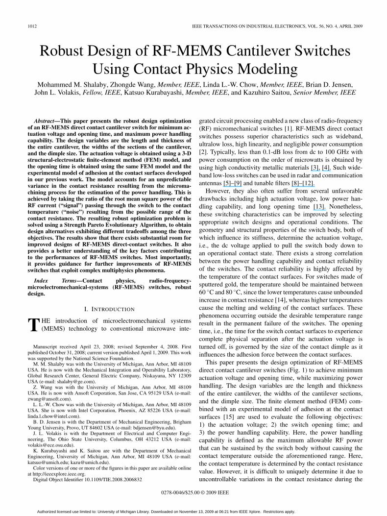
This paper presents the design optimization of RF-MEMSdirect contact cantilever switches (Fig. 1) to achieve minimumactuation voltage and opening time, while maximizing powerhandling. The design variables are the length and thicknessof the entire cantilever, the widths of the cantilever sections,and the dimple size. The finite element method (FEM) com-bined with an experimental model of adhesion at the contactsurfaces [15] are used to evaluate the following objectives:1) the actuation voltage; 2) the switch opening time; and3) the power handling capability. Here, the power handlingcapability is defined as the maximum allowable RF powerthat can be sustained by the switch body without causing thecontact temperature outside the aforementioned range. Here,the contact temperature is determined by the contact resistancevalue. However, it is difficult to uniquely determine it due touncontrollable variations in the contact resistance during the
0278-0046/$25.00 © 2009 IEEE
Authorized licensed use limited to: University of Michigan Library. Downloaded on November 13, 2009 at 06:21 from IEEE Xplore. Restrictions apply.
SHALABY et al.: ROBUST DESIGN OF RF-MEMS CANTILEVER SWITCHES USING CONTACT PHYSICS MODELING 1013
Fig. 1. RF-MEMS direct contact cantilever switch.
actual micromachining processes. Therefore, we employ thesignal-to-noise ratio model [16], [17] to estimate the powerhandling. In this model, the signal value is the root mean square(rms) power of the RF current passing through the switch,whereas the noise is the contact temperature resulting fromthe uncertainty in the contact resistance value. The resultingrobust optimization problem is solved using a Strength ParetoEvolutionary Algorithm (SPEA) [18]–[20], to obtain Pareto-optimal design alternatives exhibiting different tradeoffs amongthe three objectives.
II. RELATED WORK
A. Characterization and Modeling of RF-MEMS Switches
A number of researchers have studied the performance ofRF-MEMS switches and pointed out some unfavorable draw-backs. Chan et al. [21] and Goldsmith et al. [22]–[24] indicatedthat a high actuation voltage may lead to a shorter lifetimefor direct contact and capacitive MEMS switches which usedielectric layers for isolation. Schauwecker et al. [25] andRebeiz and Muldavin [26] point out that that the power handlingcapability is often lower than 100 mW, whereas most wirelessapplications may require 1 W.
The electromagnetic modeling of RF-MEMS switches is achallenging task due to the tiny electrical dimensions and theswitch motion during the operation [27]. Some papers suggestsolutions to these challenges, such as finite difference timedomain [28] and moment method [1], [29]. Wang et al. [27]developed an extended finite-element boundary-integral(EFE-BI) method by applying a conventional FE-BI [29] onthe substrate and a BI for the switch beam. This model wasexperimentally verified by Chow et al. [30] for air-suspendedtransmission lines. A closed-form thermal model capturing theskin effect was employed in [27] and [30]. This latter modelsaves computational time and demonstrates very reasonableaccuracy and is therefore adopted in this paper.
B. Contact Modeling for RF-MEMS Switches
Understanding the thermal and mechanical behavior of con-tact surfaces is the key to improving the performance, reliabil-ity, and power handling of RF-MEMS direct contact switches.Greenwood and Williamson developed a classical model ofcontact heating in 1958 based on the assumption that equipo-tential surfaces are coincident with the isotherms in the contact[31]. In our previous work, Jensen et al. [15] extended themodel and further demonstrated the control of the contact resis-tance by a softening temperature. When the contact temperature
exceeds the contact material softening temperature, the contactresistance drops drastically and remains low.
As expected, switch opening time is highly affected byadhesion, and most models and experiments have focused onsteady-state behavior. More recently, Jensen et al. developed akinetic model, and therefore, this model will be adopted in thispaper.
C. RF-MEMS Switch Optimization
A number of efforts have already been published on RF-MEMS optimization. Among them, Ducarouge et al. [32] de-veloped a design method for fixed–fixed RF-MEMS switchesand optimized the beam by varying three width variables.Miao et al. [33] controlled the performance of a capacitivefixed–fixed RF-MEMS switch by changing the geometry atboth ends of the beam to have smaller widths, thus reducingthe switch stiffness. Huang et al. [34] pursed a more generalapproach by dividing the beam into several sections, eachwith a different width and length to have more control on theswitch performance. The artificial neural network method wasthen used to simulate and optimize the beam [35]. The inputvariables were the beam length and width at each beam sectionwith the insertion and return loss as the output variables.
Nevertheless, none of the aforementioned models dealt withcantilever RF-MEMS switches which are known to have betterstructural properties and are less prone to buckling. Further-more, previous optimization models only handled one to threedesign objectives and few design variables.
D. Robust Design Optimization
Taguchi [16] defined robustness as the “insensitivity of thesystem performance to parameters that are uncontrollable bythe designer.” A robust design incorporates this concept of ro-bustness into design optimization and aims at achieving designsthat optimize given performance measures while minimizingsensitivities against uncontrollable parameters using differentapproaches, such as signal to noise ratio [36]–[40].
A key system parameter affecting power handling inRF-MEMS switches is contact resistance. This parameter is vir-tually impossible to precisely control during micromachining.Thus, in the following, we focus on design optimization withthe contact resistance being a free parameter.
III. ROBUST OPTIMIZATION OF RF-MEMS SWITCHES
A. Overview
The optimization problem statement for RF-MEMS directcontact cantilever switches can be summarized as follows:
• Given: switch material properties (mechanical, electrical,and thermal including), geometry of one side of cantileverbeam with parameters for optimization, contact dimple,gap length between the switch beam and the substrate, andthe acceptable range of contact resistance.
• Find: beam and dimple dimensions, and RF current.• Subject to: a feasible contact temperature accounting for
contact resistance variations.
Authorized licensed use limited to: University of Michigan Library. Downloaded on November 13, 2009 at 06:21 from IEEE Xplore. Restrictions apply.
1014 IEEE TRANSACTIONS ON INDUSTRIAL ELECTRONICS, VOL. 56, NO. 4, APRIL 2009
Fig. 2. Inputs and outputs of models used.
Fig. 3. Power handling capability factors.
• Minimize: actuation voltage and switch opening time.• Maximize: switch power handling.The optimization problem is set up via a SPEA to obtain
Pareto-optimal design alternatives exhibiting different tradeoffsamong the three objectives: actuation voltage, switch openingtime, and power handling capability.
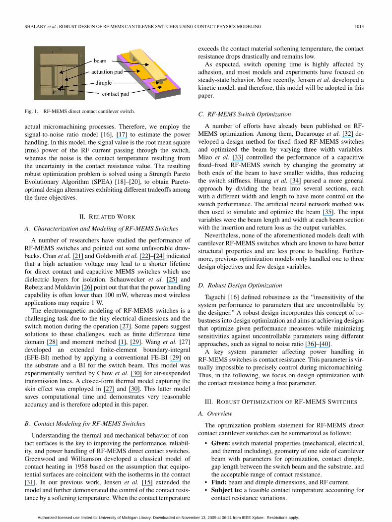
Fig. 2 shows the input–output relationships between themathematical models used to compute the three objectives.Three different computational models are employed within theoptimization loop. The actuation voltage (Vpd) is obtainedusing a 3-D structural-electrostatic FE beam model; the switchopening time (topen) evaluation is based on an experimentalcontact adhesion model from our previous work [15]. Thismodel accounts for the dimple size, contact resistance, and therestoring force (Frestore) of the beam at the down state. Finally,for power handling evaluation, an analytical model based on a2-D thermal FE model was adopted.
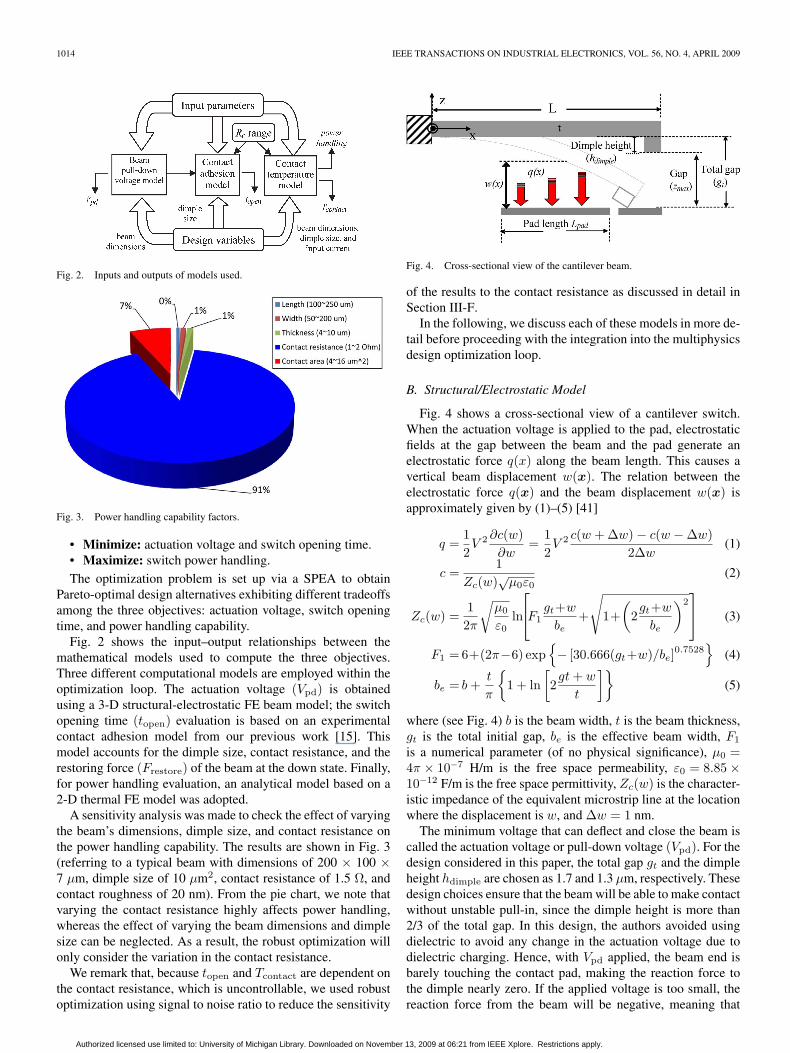
A sensitivity analysis was made to check the effect of varyingthe beam’s dimensions, dimple size, and contact resistance onthe power handling capability. The results are shown in Fig. 3(referring to a typical beam with dimensions of 200 × 100 ×7 μm, dimple size of 10 μm2, contact resistance of 1.5 Ω, andcontact roughness of 20 nm). From the pie chart, we note thatvarying the contact resistance highly affects power handling,whereas the effect of varying the beam dimensions and dimplesize can be neglected. As a result, the robust optimization willonly consider the variation in the contact resistance.
We remark that, because topen and Tcontact are dependent onthe contact resistance, which is uncontrollable, we used robustoptimization using signal to noise ratio to reduce the sensitivity
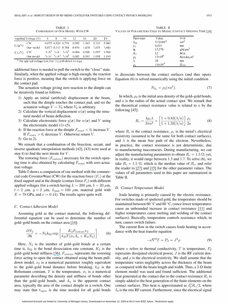
Fig. 4. Cross-sectional view of the cantilever beam.
of the results to the contact resistance as discussed in detail inSection III-F.
In the following, we discuss each of these models in more de-tail before proceeding with the integration into the multiphysicsdesign optimization loop.
B. Structural/Electrostatic Model
Fig. 4 shows a cross-sectional view of a cantilever switch.When the actuation voltage is applied to the pad, electrostaticfields at the gap between the beam and the pad generate anelectrostatic force q(x) along the beam length. This causes avertical beam displacement w(x). The relation between theelectrostatic force q(x) and the beam displacement w(x) isapproximately given by (1)–(5) [41]
q =12V 2 ∂c(w)
∂w=
12V 2 c(w + Δw) − c(w − Δw)
2Δw(1)
c =1
Zc(w)√
μ0ε0(2)
Zc(w) =12π
√μ0
ε0ln
⎡⎣F1
gt+w
be+
√1+
(2gt+w
be
)2⎤⎦ (3)
F1 = 6+(2π−6) exp{− [30.666(gt+w)/be]
0.7528}
(4)
be = b +t
π
{1 + ln
[2gt + w
t
]}(5)
where (see Fig. 4) b is the beam width, t is the beam thickness,gt is the total initial gap, be is the effective beam width, F1
is a numerical parameter (of no physical significance), μ0 =4π × 10−7 H/m is the free space permeability, ε0 = 8.85 ×10⁻¹² F/m is the free space permittivity, Zc(w) is the character-istic impedance of the equivalent microstrip line at the locationwhere the displacement is w, and Δw = 1 nm.
The minimum voltage that can deflect and close the beam iscalled the actuation voltage or pull-down voltage (Vpd). For thedesign considered in this paper, the total gap gt and the dimpleheight hdimple are chosen as 1.7 and 1.3 μm, respectively. Thesedesign choices ensure that the beam will be able to make contactwithout unstable pull-in, since the dimple height is more than2/3 of the total gap. In this design, the authors avoided usingdielectric to avoid any change in the actuation voltage due todielectric charging. Hence, with Vpd applied, the beam end isbarely touching the contact pad, making the reaction force tothe dimple nearly zero. If the applied voltage is too small, thereaction force from the beam will be negative, meaning that
Authorized licensed use limited to: University of Michigan Library. Downloaded on November 13, 2009 at 06:21 from IEEE Xplore. Restrictions apply.
SHALABY et al.: ROBUST DESIGN OF RF-MEMS CANTILEVER SWITCHES USING CONTACT PHYSICS MODELING 1015
TABLE ICOMPARISON OF OUR MODEL WITH CW
additional force is needed to pull the switch to the “close” state.Similarly, when the applied voltage is high enough, the reactionforce is positive, meaning that the switch is applying force onthe contact pad.
The actuation voltage giving zero reaction to the dimple canbe iteratively found as follows.
1) Apply an initial (artificial) displacement at the beam,such that the dimple touches the contact pad, and set theactuation voltage V = V0 where V0 is arbitrary.
2) Calculate the vertical displacement w(x) using the struc-tural model of beam deflection.
3) Calculate electrostatic force q(x) for w(x) and V usingthe electrostatic model (1)–(5).
4) If the reaction force at the dimple Freact < 0, increase V .If Freact > 0, decrease V . Otherwise return V .
5) Go to 2).
We remark that a combination of the bisection, secant, andinverse quadratic interpolation methods [42], [43] were used atstep 4) to find the next iterate for V .
The restoring force (Frestore) necessary for the switch open-ing time is also obtained by calculating Freact with zero actua-tion voltage.
Table I shows a comparison of our method with the commer-cial code CoventorWare (CW) for the reaction force (Fr) at thefixed support and at the dimple (contact force Fc) with differentapplied voltages (for a switch having L = 200 μm, b = 20 μm,t = 2 μm, g = 2 μm, Lpad = 160 μm, material gold withE = 78 GPa, and ν = 0.44). The results agree quite well.
C. Contact Adhesion Model
Assuming gold as the contact material, the following dif-ferential equation can be used to determine the number ofgold–gold bonds on the contact area [14]:
∂N2
∂ti= −N2k02 exp
[K2Frestorex2
kBT (φ1Aa + K2N2)
]. (6)
Here, N2 is the number of gold–gold bonds at a certaintime ti, k02 is the bond dissociation rate constant, K2 is thegold–gold bond stiffness [36], Frestore represents the restoringforce acting to open the contact obtained using the beam pull-down model, x2 is a numerical parameter roughly equivalentto the gold–gold bond distance before breaking, kB is theBoltzmann constant, T is the temperature, φ1 is a numericalparameter describing the density and stiffness of bonds otherthan the gold–gold bonds, and Aa is the apparent contactarea, typically the area of the contact dimple in a switch. Onemay state that topen is the time needed for all gold bonds
TABLE IIVALUES OF PARAMETERS USED TO MODEL CONTACT OPENING TIME [14]
to dissociate between the contact surfaces (and thus open).Equation (6) is solved numerically using the initial condition
N20 = ρ2(πa2). (7)
In which, ρ2 is the initial area density of the gold–gold bonds,and a is the radius of the actual contact spot. We remark thatthe theoretical contact resistance value is related to a by thefollowing [45]:
Rc =4ρeλ
3πa2+
[1 + 0.83(λ/a)1 + 1.33(λ/a)
]ρe
2a(8)
where Rc is the contact resistance, ρe is the metal’s electricalresistivity (assumed to be the same for both contact surfaces),and λ is the mean free path of the electron. Nevertheless,in practice, the contact resistance is not deterministic, dueto manufacturing inaccuracies. During manufacturing, we canadjust the manufacturing parameters to obtain Rc = 1.5 Ω; yet,in reality, it would range between 1.3 and 1.7. To solve (6), wetake Rc = 1.5 Ω, which is the median value of Rc, and referthe reader to [27] and [15] for the other parameter values. Thevalues of all parameters used in this paper are summarized inTable II.
D. Contact Temperature Model
Joule heating is primarily caused by the electric resistance.For switches made of sputtered gold, the temperature should bemaintained between 60 ◦C and 80 ◦C, (since lower temperaturescause an unbounded increase in contact resistance [11] andhigher temperatures cause melting and welding of the contactsurfaces). Basically, temperature controls resistance which, inturn, causes switch failure.
The current flow in the switch causes Joule heating in accor-dance with the heat transfer equation
−κ∇2T = Pd = J2ρ (9)
where κ refers to thermal conductivity, T is temperature, Pd
represents dissipated electrical power, J is the RF current den-sity, and ρ is the electrical resistivity. We shall assume that thetemperature varies negligibly across the thickness of the beamas compared with the beam length and width. Thus, a 2-D finiteelement model was used and found sufficient. The additionalheat generated at the contact due to the contact resistance Rc issimply added to the heat generation of the finite elements on thecontact surfaces. This heat is approximated as I2
0Rc/2, whereI0 is the rms RF current. Furthermore, since the electrical signal
Authorized licensed use limited to: University of Michigan Library. Downloaded on November 13, 2009 at 06:21 from IEEE Xplore. Restrictions apply.
1016 IEEE TRANSACTIONS ON INDUSTRIAL ELECTRONICS, VOL. 56, NO. 4, APRIL 2009
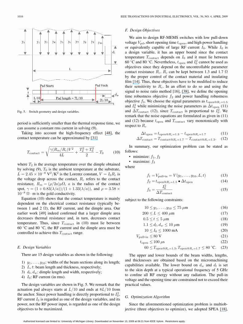
Fig. 5. Switch geometry and design variables.
period is sufficiently smaller than the thermal response time, wecan assume a constant rms current in solving (9).
Taking into account the high-frequency effect [48], thecontact temperature can be approximated by [31]
Tcontact =
√γ(Rm/Rc)V 2
4L+
T 22 + T 2
0
2− T0 (10)
where T2 is the average temperature over the dimple obtainedby solving (9), T0 is the ambient temperature at the substrate,L = 2.45 × 10⁻⁸ V2/K2 is the Lorentz constant, V = I0Rc isthe voltage drop across the contact, Rc refers to the contactresistance, Rm = (ρ/2a)μΩ, a is the radius of the contactspot, γ = (1 + 0.83(λ/a))/(1 + 1.33(λ/a)), and ρ = 3.58 ×10⁻⁸ Ω · m is the gold conductivity.
Equation (10) shows that the contact temperature is mainlydependent on the electrical contact resistance (typically be-tween 1 and 2 Ω), the RF current, and the dimple area. Ourearlier work [49] indeed confirmed that a larger dimple areadecreases thermal resistance and, in turn, decreases contacttemperature. Thus, since Tcontact in (10) must lie between60 ◦C and 80 ◦C, the RF current and the dimple area must becontrolled to achieve this Tcontact range.
E. Design Variables
There are 15 design variables as shown in the following:
1) y1, . . . , y10: widths of the beam sections along its length;2) L, t: beam length and thickness, respectively;3) dl, dw: dimple length and width, respectively;4) I0: RF current (in rms).
The design variables are shown in Fig. 5. We remark that theactuation pad always starts at L/10 and ends at 8L/10 fromthe anchor. Since power handling is directly proportional to I2
0 ,RF current I0 is regarded as one of the design variables, and itspower, not the RF power input, is regarded as one of the designobjectives to be maximized.
F. Design Objectives
We aim to design RF-MEMS switches with low pull-downvoltage Vpd, short opening time topen, and high power handlingor equivalently capable of large RF current I0. While I0 isa design variable, it has an upper bound since the contacttemperature Tcontact depends on I0 and it must lie between60 ◦C and 80 ◦C. Nevertheless, topen and I2
0 cannot be used asobjectives since they depend on the uncontrollable parametercontact resistance Rc. Rc can be kept between 1.3 and 1.7 Ωby the proper control of the contact material and insulatingfilm [14]. Thus, these objectives have to be modified to reducetheir sensitivity to Rc. In an effort to do so and using thesignal to noise ratio method [16], [38], we define the openingtime robustness objective f2 and power handling robustnessobjective f3. We choose the signal parameters as topen@Rc=1.5
and I20 while minimizing the noise parameters as Δtopen (11)
and ΔTcontact (12), since Tcontact is proportional to I20 . We
remark that the noise equations are formulated as given in (11)and (12) because topen and Tcontact vary monotonically withrespect to Rc
Δtopen = topen@Rc=1.3 − topen@Rc=1.7 (11)ΔTcontact = Tcontact@Rc=1.7 − Tcontact@Rc=1.3. (12)
In summary, our optimization problem can be stated asfollows:
• minimize: f1, f2
• maximize: f3
where
f1 = Vpull-in = V (y1, . . . , y10, L, t) (13)
f2 = topen@Rc=1.5 • Δtopen (14)
f3 =I20
ΔTcontact(15)
subject to the following constraints:
10 ≤ y1, . . . , y10 ≤ 75 μm (16)
200 ≤L ≤ 400 μm (17)
0.5 ≤ t ≤ 5 μm (18)
1.1 ≤ dl, dw ≤ 10 μm (19)
10 ≤ I0 ≤ 1000 mA (20)
Vpull-in ≤ 80 V (21)
topen ≤ 100 μs (22)
60 ≤Topen@Rc=1.3, Topen@Rc=1.7 ≤ 80 ◦C. (23)
The upper and lower bounds of the beam widths, lengths,and thicknesses are obtained based on the micromachiningcapabilities available. The lower bound on dw and dl is setto the skin depth at a typical operational frequency of 5 GHzto confine all RF energy without any radiation. The pull-involtage and the opening time are constrained not to exceed theirpractical values.
G. Optimization Algorithm
Since the aforementioned optimization problem is multiob-jective (three objectives to optimize), we adopted SPEA [18],
Authorized licensed use limited to: University of Michigan Library. Downloaded on November 13, 2009 at 06:21 from IEEE Xplore. Restrictions apply.
SHALABY et al.: ROBUST DESIGN OF RF-MEMS CANTILEVER SWITCHES USING CONTACT PHYSICS MODELING 1017
TABLE IIIPARAMETERS FOR SPEA
[20] to find the tradeoff among the various conflicting designobjectives. SPEA has several advantages over the conventionalmultiobjective genetic algorithms, namely, 1) dominating so-lutions are sorted externally in a second continuously updatedpopulation, 2) the fitness of each individual in the normal pop-ulation is evaluated with respect to the number of dominatingpoints in the external population that dominate that individual,3) Pareto dominance preserves the population diversity, and4) a clustering procedure is used to reduce the dominatingset without destroying its characteristics [18]. In the imple-mentation of SPEA, side constraints (16)–(20) are embeddedin the chromosome encoding of the algorithm, whereas con-straints (21)–(23) are handled as penalties on their objectivefunctions. The parameters used in the SPEA are summarizedin Table III.
IV. RESULTS AND DISCUSSION
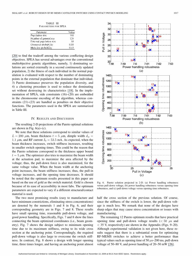
The resulting 2-D projections of the Pareto optimal solutionsare shown in Fig. 6(a)–(c).
We note that these solutions correspond to similar values ofL = 200 μm, beam thickness t = 5 μm, dimple width dw =1.1 μm, and RF current I0 = 53.5 mA. As expected, when thebeam thickness increases, switch stiffness increases, resultingin smaller switch opening times. This could be the reason thatthe Pareto solutions correspond to the thickness upper boundt = 5 μm. The optimizer also tries to maximize the beam widthat the actuation pad, to maximize the area affected by thevoltage; thus, the pull-down force is also maximized, for thesame voltage value. When the beam width at the anchoringpoint increases, the beam stiffness increases; thus, the pull-involtage increases, and the opening time decreases. It shouldbe noted that the optimum results presented in this paper arebased on the use of gold as the switch material. Gold is chosenbecause of its ease of accessibility in most fabs. The optimumparameters are expected to vary if a different structural/contactmaterial is used.
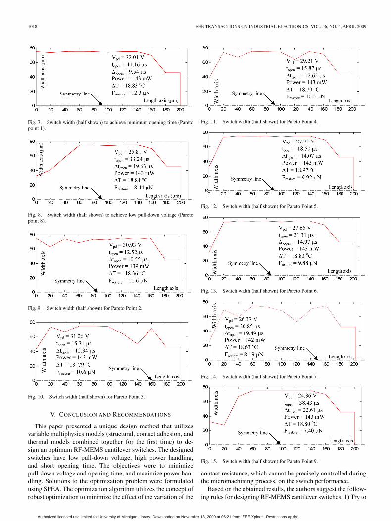
The two most promising results (easy to manufacture andhave minimum constrictions, eliminating stress concentrations)are denoted by the numerals 1 and 8 in Fig. 6, and theircorresponding geometry are in Figs. 7 and 8. These resultshave small opening time, reasonable pull-down voltage, andgood power handling. Specifically, Figs. 7 and 8 show the linesconnecting the beam optimized coordinates (i.e., beam geom-etry). Fig. 7 shows the design subject to minimum openingtime due to its maximum stiffness, owing to its wide crosssection at the anchoring point. Correspondingly, the requiredpull-down voltage is also large to overcome the switch stiff-ness. In contrast, Fig. 8 shows a design with longer openingtime, three times longer, and having an anchoring point almost
Fig. 6. Pareto solution projected in 2-D. (a) Power handling robustnessversus pull-down voltage, (b) power handling robustness versus opening timerobustness, and (c) pull-down voltage versus opening time robustness.
half the cross section of the previous solution. Of course,since the stiffness of the switch is lower, the pull-down volt-age is much less. We remark that none of the designs havesharp edges that may cause stress concentration or issues withmanufacturing.
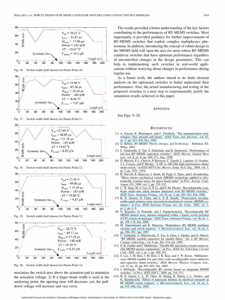
The remaining 12 Pareto optimum results that have practicalopening time and pull-down voltage results (< 50 μs and< 35 V, respectively) are shown in the Appendix (Figs. 9–20).Although experimental validation is not given here, these re-sults suggest that there is a substantial room for optimizingRF-MEMS switches to achieve a better performance thantypical values such as opening time of 50 μs–200 ms, pull-downvoltage of 50–80 V, and power handling of 20–50 mW [26].
Authorized licensed use limited to: University of Michigan Library. Downloaded on November 13, 2009 at 06:21 from IEEE Xplore. Restrictions apply.
1018 IEEE TRANSACTIONS ON INDUSTRIAL ELECTRONICS, VOL. 56, NO. 4, APRIL 2009
Fig. 7. Switch width (half shown) to achieve minimum opening time (Paretopoint 1).
Fig. 8. Switch width (half shown) to achieve low pull-down voltage (Paretopoint 8).
Fig. 9. Switch width (half shown) for Pareto Point 2.
Fig. 10. Switch width (half shown) for Pareto Point 3.
V. CONCLUSION AND RECOMMENDATIONS
This paper presented a unique design method that utilizesvariable multiphysics models (structural, contact adhesion, andthermal models combined together for the first time) to de-sign an optimum RF-MEMS cantilever switches. The designedswitches have low pull-down voltage, high power handling,and short opening time. The objectives were to minimizepull-down voltage and opening time, and maximize power han-dling. Solutions to the optimization problem were formulatedusing SPEA. The optimization algorithm utilizes the concept ofrobust optimization to minimize the effect of the variation of the
Fig. 11. Switch width (half shown) for Pareto Point 4.
Fig. 12. Switch width (half shown) for Pareto Point 5.
Fig. 13. Switch width (half shown) for Pareto Point 6.
Fig. 14. Switch width (half shown) for Pareto Point 7.
Fig. 15. Switch width (half shown) for Pareto Point 9.
contact resistance, which cannot be precisely controlled duringthe micromachining process, on the switch performance.
Based on the obtained results, the authors suggest the follow-ing rules for designing RF-MEMS cantilever switches. 1) Try to
Authorized licensed use limited to: University of Michigan Library. Downloaded on November 13, 2009 at 06:21 from IEEE Xplore. Restrictions apply.
SHALABY et al.: ROBUST DESIGN OF RF-MEMS CANTILEVER SWITCHES USING CONTACT PHYSICS MODELING 1019
Fig. 16. Switch width (half shown) for Pareto Point 10.
Fig. 17. Switch width (half shown) for Pareto Point 11.
Fig. 18. Switch width (half shown) for Pareto Point 12.
Fig. 19. Switch width (half shown) for Pareto Point 13.
Fig. 20. Switch width (half shown) for Pareto Point 14.
maximize the switch area above the actuation pad to minimizethe actuation voltage. 2) If a larger beam width is used at theanchoring point, the opening time will decrease; yet, the pull-down voltage will increase and vice versa.
The results provided a better understanding of the key factorscontributing to the performances of RF-MEMS switches. Mostimportantly, it provided guidance for further improvements ofRF-MEMS switches that exploit complex multiphysics phe-nomena. In addition, introducing the concept of robust design inthe MEMS field will open the area for more robust RF-MEMScantilever switches that have optimum performance regardlessof uncontrolled changes in the design parameters. This canhelp in implementing such switches in real-world appli-cations without worrying about changes in performance duringregular use.
As a future work, the authors intend to do finite elementanalysis on the optimized switches to better understand theirperformance. Also, the actual manufacturing and testing of theproposed switches is a next step to experimentally justify thesimulation results achieved in this paper.
APPENDIX
See Figs. 9–20.
REFERENCES
[1] A. Frazier, R. Warrington, and C. Friedrich, “The miniaturization tech-nologies: Past, present, and future,” IEEE Trans. Ind. Electron., vol. 42,no. 5, pp. 423–430, Oct. 1995.
[2] G. Rebeiz, RF MEMS: Theory, Design, and Technology. Hoboken, NJ:Wiley, 2002.
[3] C. Goldsmith, Z. Yao, S. Eshelman, and D. Denniston, “Performance oflow-loss RF MEMS capacitive switches,” IEEE Microw. Guided WaveLett., vol. 8, no. 8, pp. 269–271, Aug. 1998.
[4] D. Mercier, P. L. Charvet, P. Berruyer, C. Zanchi, L. Lapierre, O. Vendier,J. L. Cazaux, and P. Blondy, “A DC to 100 GHz high performance ohmicshunt switch,” in IEEE MTT-S Int. Microw. Symp. Tech. Dig., 2004, vol. 3,pt. 3, pp. 1931–1934.
[5] B. Norvell, R. Hancock, J. Smith, M. Pugh, S. Theis, and J. Kviatkofsky,“Micro electro mechanical switch (MEMS) technology applied to elec-tronically scanned arrays for space based radar,” in Proc. Aerosp. Conf.,Aspen, CO, 1999, vol. 3, pp. 239–247.
[6] C. W. Jung, M.-J. Lee, G. P. Li, and F. De Flaviis, “Reconfigurable scan-beam single-arm spiral antenna integrated with RF-MEMS switches,”IEEE Trans. Antennas Propag., vol. 54, no. 2, pp. 455–463, Feb. 2006.
[7] R. N. Simons, D. Chun, and L. P. B. Katehi, “Polarization reconfig-urable patch antenna using microelectromechanical systems (MEMS) ac-tuators,” in Proc. IEEE Antennas Propag. Soc. Int. Symp., 2002, vol. 2,pt. 2, pp. 6–9.
[8] N. Kingsley, G. Ponchak, and J. Papapolymerou, “Reconfigurable RFMEMS phased array antenna integrated within a liquid crystal polymer(LCP) system-on-package,” IEEE Trans. Antennas Propag., vol. 56, no. 1,pp. 108–118, Jan. 2008.
[9] M. Daneshmand and R. Mansour, “Redundancy RF MEMS multiportswitches and switch matrices,” J. Microelectromech. Syst., vol. 16, no. 2,pp. 296–303, Apr. 2007.
[10] C. Goldmith, A. Malczewski, Z. Yao, S. Chen, J. Ehmke, and D. Hinzel,“RF MEMS variable capacitors for tunable filters,” Int. J. RF Microw.Comput.-Aided Eng., vol. 9, pp. 362–374, Jul. 1999.
[11] G. K. Fedder and T. Mukherjee, “Tunable RF and analog circuits using on-chip MEMS passive components,” in Proc. IEEE Int. Solid-State CircuitsConf., 2005, vol. 1, pt. 1, pp. 390–391.
[12] S. Lee, J.-M. Kim, J.-M. Kim, J. K. Kim, and Y. W. Kwon, “Millimeter-wave MEMS tunable low pass filter with reconfigurable series inductorsand capacitive shunt switches,” IEEE Microw. Wireless Compon. Lett.,vol. 15, no. 10, pp. 691–693, Oct. 2005.
[13] J. DeNatale, “Reconfigurable RF circuits based on integrated MEMSswitches,” in Proc. IEEE ISSCC, 2004, pp. 310–311.
[14] B. D. Jensen, L. L. W. Chow, K. Huang, K. Saitou, J. L. Volakis, andK. Kurabayashi, “Effect of nanoscale heating on electrical transport inRF MEMS switch contacts,” J. Microelectromech. Syst., vol. 14, no. 5,pp. 935–946, Oct. 2005.
Authorized licensed use limited to: University of Michigan Library. Downloaded on November 13, 2009 at 06:21 from IEEE Xplore. Restrictions apply.
1020 IEEE TRANSACTIONS ON INDUSTRIAL ELECTRONICS, VOL. 56, NO. 4, APRIL 2009
[15] B. Jensen, K. Huang, L. L.-W. Chow, and K. Kurabayashi, “Adhesioneffects on contact opening dynamics in micromachined switches,” J. Appl.Phys., vol. 97, no. 10, pp. 103 535-1–103 535-9, May 2005.
[16] G. Taguchi, Systems of Experimental Design. New York: Kraus Int.,1987.
[17] S. Tsutsui and A. Ghosh, “Genetic algorithms with a robust solutionsearching scheme,” IEEE Trans. Evol. Comput., vol. 1, no. 3, pp. 201–208, Sep. 1997.
[18] E. Zitzler and L. Thiele, “Multiobjective evolutionary algorithms: A com-parative case study and the strength Pareto approach,” IEEE Trans. Evol.Comput., vol. 3, no. 4, pp. 257–271, Nov. 1999.
[19] F. Mendoza, J. Bernal-Agustin, and J. Dominguez-Navarro, “NSGA andSPEA applied to multiobjective design of power distribution systems,”IEEE Trans. Power Syst., vol. 21, no. 4, pp. 1938–1945, Nov. 2006.
[20] C. Coello, D. Veldhuizen, and G. Lamont, Evolutionary Algorithms forSolving Multi-Objective Problems. Norwell, MA: Kluwer, 2002.
[21] R. Chan, R. Lesnick, D. Becher, and M. Feng, “Low-actuation voltage RFMEMS shunt switch with cold switching lifetime of seven billion cycles,”J. Microelectromech. Syst., vol. 12, no. 5, pp. 713–719, Oct. 2003.
[22] C. Goldsmith, J. Ehmke, A. Malczewski, B. Pillans, S. Eshelman,Z. Yao, J. Brank, and M. Eberly, “Lifetime characterization of capacitiveRF MEMS switches,” in IEEE MTT-S Int. Microw. Symp. Tech. Dig.,Phoenix, AZ, 2001, vol. 3, pp. 227–230.
[23] C. Goldsmith, J. Maciel, and J. McKillop, “Demonstrating reliability,”IEEE Microw. Mag., vol. 8, no. 6, pp. 56–60, Dec. 2007.
[24] C. Goldsmith, D. Forehand, Z. Peng, J. Hwang, and I. Ebel, “High-cyclelife testing of RF MEMS switches,” in IEEE MTT-S Int. Microw. Symp.Tech. Dig., Jun. 2007, pp. 1805–1808.
[25] B. Schauwecker, K. Strohm, W. Simon, J. Mehner, and J. Luy, “Toggle-switch—A new type of RF MEMS switch for power applications,” inIEEE MTT-S Int. Microw. Symp. Tech. Dig., Seattle, WA, 2002, vol. 1,pp. 219–222.
[26] G. Rebeiz and J. Muldavin, “RF MEMS switches and switch circuits,”IEEE Microw. Mag., vol. 2, no. 4, pp. 59–71, Dec. 2001.
[27] Z. Wang, B. Jensen, L. L.-W. Chow, J. Volakis, K. Saitou, andK. Kurabayashi, “Full-wave electromagnetic and thermal modeling forthe prediction of heat-dissipation-induced RF-MEMS switch failure,”J. Micromech. Microeng., vol. 16, no. 1, pp. 157–164, Jan. 2006.
[28] W. Thiel, K. Tornquist, R. Reano, and L. Katehi, “A study of thermaleffects in RF-MEM-switches using a time domain approach,” in IEEEMTT-S Int. Microw. Symp. Tech. Dig., Seattle, WA, 2002, pp. 235–238.
[29] J. Volakis, A. Chatterjee, and L. Kempel, Finite Element Method of Elec-tromagnetics. New York: IEEE Press, 1998.
[30] L. L.-W. Chow, Z. Wang, B. Jensen, K. Saitou, J. Volakis, andK. Kurabayashi, “Skin-effect self-heating in air-suspended RF MEMStransmission-line structures,” J. Microelectromech. Syst., vol. 15, no. 6,pp. 1622–1631, Dec. 2006.
[31] J. A. Greenwood and J. B. P. Williamson, “Electrical conduction in solids.II. Theory of temperature-dependent conductors,” Proc. R. Soc. Lond. A,Math. Phys. Sci., vol. 246, no. 1244, pp. 13–31, Jul. 1958.
[32] B. Ducarouge, D. Dubuc, S. Melle, K. Grenier, L. Mazenq, L. Bary, andR. Plana, “Efficient topology and design methodology for RF MEMSswitches,” in Proc. SPIE—Int. Soc. Opt. Eng., Smart Sens., Actuators,MEMS II, Seville, Spain, May 9–11, 2005, vol. 5836, pp. 535–539.
[33] M. Miao, Z. Xiao, G. Wu, Y. Hao, and H. Zhang, “Capacitive RFMEMS switch with composite beam,” in Proc. SPIE—Int. Soc. Opt.Eng., MEMS/MOEMS Technol. Appl., China, Oct. 17–18, 2002, vol. 4928,pp. 248–255.
[34] J. Huang, K. Liew, C. Wong, S. Rajendran, M. Tan, and A. Liu, “Mechan-ical design and optimization of capacitive micromachined switch,” Sens.Actuators A, Phys., vol. 93, no. 3, pp. 273–285, Oct. 2001.
[35] Y. Lee and D. Filipovic, “ANN based electromagnetic models for thedesign of RF MEMS switches,” IEEE Microw. Wireless Compon. Lett.,vol. 15, no. 11, pp. 823–825, Nov. 2005.
[36] J. Che, G. Xian, and E. Knod, “An integrated design method of newproduct and the production process based on Taguchi robust design,” inProc. 2nd IEEE Conf. Ind. Electron. Appl., Harbin, China, May 23–25,2007, pp. 1437–1442.
[37] R. Al-Aomar, “Incorporating robustness into genetic algorithm searchof stochastic simulation outputs,” Simul. Model. Pract. Theory, vol. 14,no. 3, pp. 201–223, Apr. 2006.
[38] I. Madu and C. Madu, “Design optimization using signal-to-noise ratio,”Simul. Pract. Theory, vol. 7, no. 4, pp. 349–372, Jun. 1999.
[39] W. Fowlkes and M. Clyde, Engineering Methods for Robust ProductDesign. Reading, MA: Addison-Wesley, 1995.
[40] B. Ramakrishnan and S. Rao, “A robust optimization approach usingTaguchi’s loss function for solving nonlinear optimization problems,”
ASME Des. Eng. Div. Publ. DE, Adv. Des. Autom., vol. 1, no. 32, pp. 241–248, Sep. 22–25, 1991.
[41] F. Gardiol, Microstrip Circuits. New York: Wiley, 1994.[42] MATLAB R14 V7.1, 1984–2005, Natick, MA: MathWorks, Inc. [Online].
Available: www.mathworks.com[43] G. Forsythe, M. Malcolm, and C. Moler, Computer Methods for Mathe-
matical Computations. Englewood Cliffs, NJ: Prentice–Hall, 1976.[44] G. Rubio-Bollinger, S. R. Bahn, N. Agraït, K. W. Jacobsen, and S. Vieira,
“Mechanical properties and formation mechanisms of a wire of singlegold atoms,” Phys. Rev. Lett., vol. 87, no. 2, pp. 026 101-1–026 101-2,Jul. 2001.
[45] B. Nikolic and P. Allen, “Electron transport through a circular constric-tion,” Phys. Rev. B, Condens. Matter, vol. 60, no. 6, pp. 3963–3969,Aug. 1999.
[46] R. Timsit, “Electrical contact resistance: Properties of stationary inter-faces,” IEEE Trans. Compon. Packag. Technol., vol. 22, no. 1, pp. 85–98,Mar. 1999.
[47] R. Holm, Electrical Contacts, Theory and Applications. Berlin,Germany: Springer-Verlag, 1976.
[48] B. Jensen, K. Huang, L. L.-W. Chow, and K. Kurabayashi, “Low-force contact heating and softening using micromechanical switches indiffusive-ballistic electron-transport transition,” Appl. Phys. Lett., vol. 86,no. 2, pp. 023 507-1–023 507-3, Jan. 2005.
[49] Z. Wang, “Integrated electromagnetic/thermal/mechanical analysis andoptimization design of RF-MEMS switches,” Ph.D. dissertation, Univ.Michigan, Ann Arbor, MI, 2005.
Mohammed M. Shalaby received the B.S. and M.S.degrees from Cairo University, Cairo, Egypt, in 2000and 2002, respectively, and the Ph.D. degree from theUniversity of Michigan, Ann Arbor, in 2008, all inmechanical engineering.
Since February 2008, he has been with theGlobal Research Center, General Electric Company,Niskayuna, NY, as a Mechanical Engineer in the Me-chanical Integration and Operability Laboratory. Hehas published over 20 conference/journal papers inthe areas of design for disassembly, RF-MEMS, and
reverse engineering. His current research interests are developing CAD toolsfor the automation of the design process, design automation and optimization,design for disassembly, and optimization of MEMS components.
Zhongde Wang (M’04) received the M.S. degreefrom the University of Waterloo, Waterloo, ON,Canada, in 2002, and the Ph.D. degree from theUniversity of Michigan, Ann Arbor, in 2005, both inelectrical engineering.
Since January 2005, he has been with AnsoftCorporation (now part of Ansys Inc.), San Jose,CA, as an Application Engineer. He has authoredor coauthored over 20 technical papers. His currentresearch focuses on computational electromagneticswith applications in antenna/microwave component
design, RF-MEMS switches, the signal and power integrities of printed circuitboards and packages, etc.
Dr. Wang was the recipient of the second-grade prize of the Science andTechnology Progress awarded by the Chinese Electrical Ministry in 1996.
Linda L.-W. Chow (S’02–M’06) received the Ph.D.degree from the University of Michigan, Ann Arbor,in 2006.
She has been a Packaging Engineer with IntelCorporation, Phoenix, AZ, since her graduation. Shehas published over 20 conference/journal papers inthe areas of sensors, RF-MEMS, packaging, andreliability physics. She is also the holder of twopatents, one pending patent, and three trade secrets.
Dr. Chow was awarded with Best Teaching As-sistant twice and Best Student Paper at the IEEE
International Symposium on Electronic Materials and Packaging in 2000.
Authorized licensed use limited to: University of Michigan Library. Downloaded on November 13, 2009 at 06:21 from IEEE Xplore. Restrictions apply.
SHALABY et al.: ROBUST DESIGN OF RF-MEMS CANTILEVER SWITCHES USING CONTACT PHYSICS MODELING 1021
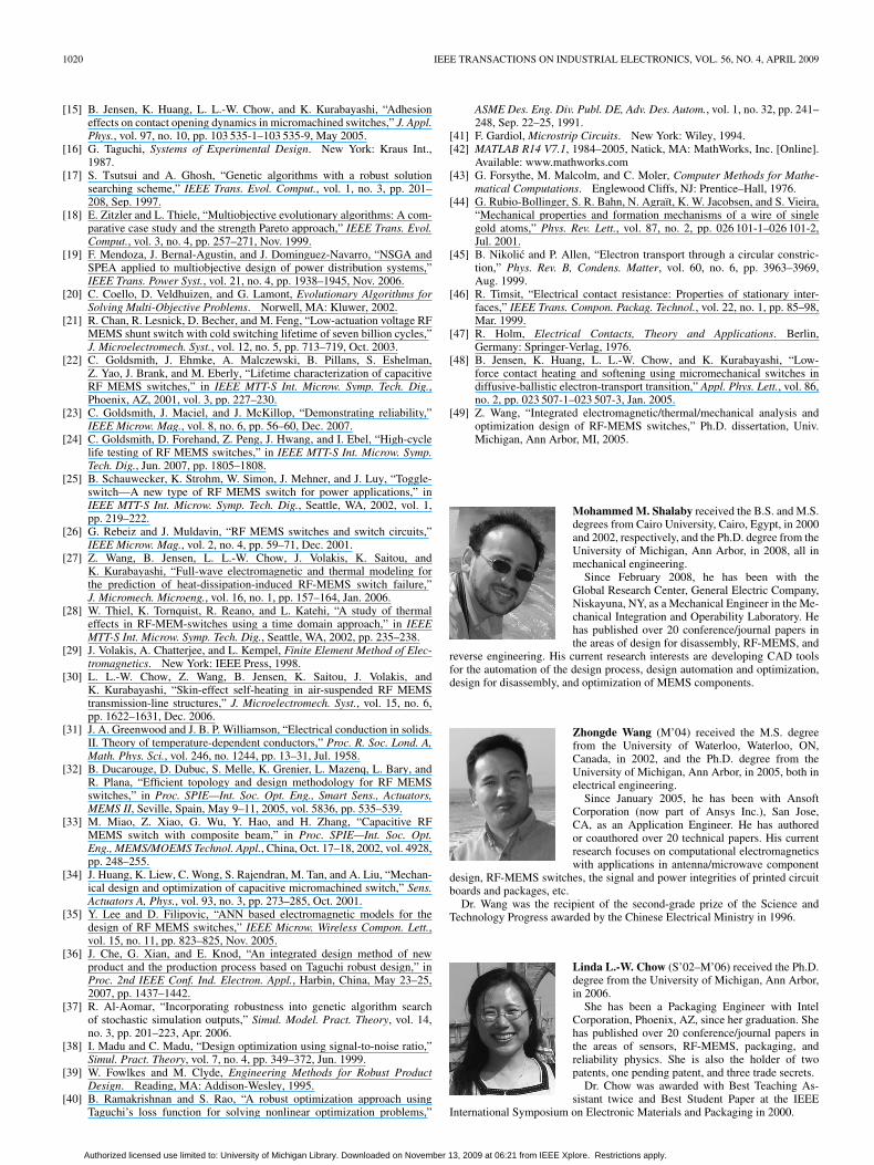
Brian D. Jensen received the B.S. and M.S. degreesin mechanical engineering from Brigham YoungUniversity, Provo, UT, in 1996 and 1998, respec-tively, and the M.S. and Ph.D. degrees in electricaland mechanical engineering, respectively, from theUniversity of Michigan, Ann Arbor, both in 2004.
He has been with the Department of Mechani-cal Engineering, Brigham Young University, sinceJanuary 2005. In 1998 and 1999, he spent 16 monthsas a Micromechanism Designer with Sandia NationalLaboratories, Albuquerque, NM. He has performed
research and published over 50 papers on a wide variety of design topics,including microelectromechanical systems and compliant mechanisms, and heis the holder of seven U.S. patents.
Dr. Jensen was the recipient of a National Science Foundation GraduateResearch Fellowship and a Department of Defense Science and EngineeringGraduate Fellowship.
John L. Volakis (S’77–M’82–SM’89–F’96) wasborn on May 13, 1956 in Chios, Greece, and im-migrated to the U.S. in 1973. He received the B.E.degree (summa cum laude) from Youngstown StateUniversity, Youngstown, OH, in 1978, and the M.Sc.and Ph.D. degrees from The Ohio State University,Columbus, in 1979 and 1982, respectively.
He was with Rockwell International (1982–1984),now Boeing Phantom Works, Seal Beach, CA. In1984, he was appointed Assistant Professor at theUniversity of Michigan (UM), Ann Arbor, becoming
a Full Professor in 1994. He was also the Director of the Radiation Laboratoryfrom 1998 to 2000. Since January 2003, he has been the Roy and Lois ChopeChair Professor of Engineering with The Ohio State University and the Directorof the ElectroScience Laboratory, Department of Electrical and ComputerEngineering. He has published over 250 articles in major refereed journals,nearly 380 conference papers, and 20 book chapters. He is a coauthor of thefollowing four books: Approximate Boundary Conditions in Electromagnetics(IEE, 1995), Finite Element Method for Electromagnetics (IEEE Press, 1998),Frequency Domain Hybrid Finite Element Methods in Electromagnetics (Mor-gan & Claypool, 2006), and Antenna Engineering Handbook (McGraw-Hill,2007), of which he was also the Editor. He was the Associate Editor of RadioScience from 1994 to 1997 and, currently, is an Associate Editor for the Journalof Electromagnetic Waves and Applications and the Union Radio ScientificInternational (URSI) Bulletin. He has also written several well-edited coursepa-cks on introductory and advanced numerical methods for electromagnetics andhas delivered short courses on antennas, numerical methods, and frequency-selective surfaces. He is listed by ISI Web of Knowledge among the top 250most referenced authors. He graduated/mentored nearly 60 Ph.D. students/postdocs and coauthored with them nine papers that received best paperawards at conferences. His primary research deals with antennas, computationalmethods, electromagnetic compatibility and interference, propagation, designoptimization, RF materials, multiphysics engineering, and bioelectromagnetics.
Dr. Volakis is a member of the URSI Commissions B and E. He was the2004 President of the IEEE Antennas and Propagation Society and servedon the AdCom of the IEEE Antennas and Propagation Society from 1995 to1998. He also served as Associate Editor for the IEEE TRANSACTIONS ON
ANTENNAS AND PROPAGATION from 1988 to 1992 and for the IEEE Antennasand Propagation Magazine (1992–2006). He chaired the 1993 IEEE Antennasand Propagation Society Symposium and Radio Science Meeting in Ann Arbor,MI, and cochaired the same symposium in 2003 in Columbus, OH. He wasthe recipient of the UM College of Engineering Research Excellence Award in1998 and the UM Department of Electrical Engineering and Computer ScienceService Excellence Award in 2001.
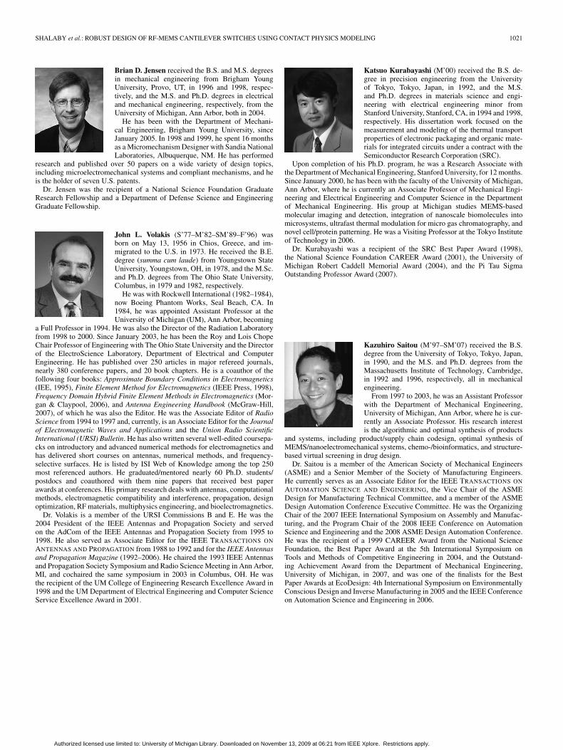
Katsuo Kurabayashi (M’00) received the B.S. de-gree in precision engineering from the Universityof Tokyo, Tokyo, Japan, in 1992, and the M.S.and Ph.D. degrees in materials science and engi-neering with electrical engineering minor fromStanford University, Stanford, CA, in 1994 and 1998,respectively. His dissertation work focused on themeasurement and modeling of the thermal transportproperties of electronic packaging and organic mate-rials for integrated circuits under a contract with theSemiconductor Research Corporation (SRC).
Upon completion of his Ph.D. program, he was a Research Associate withthe Department of Mechanical Engineering, Stanford University, for 12 months.Since January 2000, he has been with the faculty of the University of Michigan,Ann Arbor, where he is currently an Associate Professor of Mechanical Engi-neering and Electrical Engineering and Computer Science in the Departmentof Mechanical Engineering. His group at Michigan studies MEMS-basedmolecular imaging and detection, integration of nanoscale biomolecules intomicrosystems, ultrafast thermal modulation for micro gas chromatography, andnovel cell/protein patterning. He was a Visiting Professor at the Tokyo Instituteof Technology in 2006.
Dr. Kurabayashi was a recipient of the SRC Best Paper Award (1998),the National Science Foundation CAREER Award (2001), the University ofMichigan Robert Caddell Memorial Award (2004), and the Pi Tau SigmaOutstanding Professor Award (2007).
Kazuhiro Saitou (M’97–SM’07) received the B.S.degree from the University of Tokyo, Tokyo, Japan,in 1990, and the M.S. and Ph.D. degrees from theMassachusetts Institute of Technology, Cambridge,in 1992 and 1996, respectively, all in mechanicalengineering.
From 1997 to 2003, he was an Assistant Professorwith the Department of Mechanical Engineering,University of Michigan, Ann Arbor, where he is cur-rently an Associate Professor. His research interestis the algorithmic and optimal synthesis of products
and systems, including product/supply chain codesign, optimal synthesis ofMEMS/nanoelectromechanical systems, chemo-/bioinformatics, and structure-based virtual screening in drug design.
Dr. Saitou is a member of the American Society of Mechanical Engineers(ASME) and a Senior Member of the Society of Manufacturing Engineers.He currently serves as an Associate Editor for the IEEE TRANSACTIONS ON
AUTOMATION SCIENCE AND ENGINEERING, the Vice Chair of the ASMEDesign for Manufacturing Technical Committee, and a member of the ASMEDesign Automation Conference Executive Committee. He was the OrganizingChair of the 2007 IEEE International Symposium on Assembly and Manufac-turing, and the Program Chair of the 2008 IEEE Conference on AutomationScience and Engineering and the 2008 ASME Design Automation Conference.He was the recipient of a 1999 CAREER Award from the National ScienceFoundation, the Best Paper Award at the 5th International Symposium onTools and Methods of Competitive Engineering in 2004, and the Outstand-ing Achievement Award from the Department of Mechanical Engineering,University of Michigan, in 2007, and was one of the finalists for the BestPaper Awards at EcoDesign: 4th International Symposium on EnvironmentallyConscious Design and Inverse Manufacturing in 2005 and the IEEE Conferenceon Automation Science and Engineering in 2006.
Authorized licensed use limited to: University of Michigan Library. Downloaded on November 13, 2009 at 06:21 from IEEE Xplore. Restrictions apply.
Related Documents