1 23 Microsystem Technologies Micro- and Nanosystems Information Storage and Processing Systems ISSN 0946-7076 Microsyst Technol DOI 10.1007/s00542-013-1753-8 RF MEMS switches fabrication by using SU-8 technology Andrea Lucibello, Emanuela Proietti, Flavio Giacomozzi, Romolo Marcelli, Giancarlo Bartolucci & Giorgio De Angelis

Welcome message from author
This document is posted to help you gain knowledge. Please leave a comment to let me know what you think about it! Share it to your friends and learn new things together.
Transcript
1 23
Microsystem TechnologiesMicro- and Nanosystems InformationStorage and Processing Systems ISSN 0946-7076 Microsyst TechnolDOI 10.1007/s00542-013-1753-8
RF MEMS switches fabrication by usingSU-8 technology
Andrea Lucibello, Emanuela Proietti,Flavio Giacomozzi, Romolo Marcelli,Giancarlo Bartolucci & Giorgio DeAngelis

1 23
Your article is protected by copyright and
all rights are held exclusively by Springer-
Verlag Berlin Heidelberg. This e-offprint is
for personal use only and shall not be self-
archived in electronic repositories. If you
wish to self-archive your work, please use the
accepted author’s version for posting to your
own website or your institution’s repository.
You may further deposit the accepted author’s
version on a funder’s repository at a funder’s
request, provided it is not made publicly
available until 12 months after publication.

TECHNICAL PAPER
RF MEMS switches fabrication by using SU-8 technology
Andrea Lucibello • Emanuela Proietti •
Flavio Giacomozzi • Romolo Marcelli •
Giancarlo Bartolucci • Giorgio De Angelis
Received: 12 July 2012 / Accepted: 10 February 2013
� Springer-Verlag Berlin Heidelberg 2013
Abstract In this paper we present a novel process based
on SU-8 technology for the fabrication of double clamped
radio frequency (RF) micro-electro-mechanical system
(MEMS) capacitive shunt switches in coplanar configura-
tion. The key element of the exploited process is the
MicroChem SU-8 2002 negative photoresist. The poly-
meric material is widely used in MEMS device processes
because of its excellent thermal and chemical stability. In
this paper, SU-8 polymer has been utilized in a double way
to get suspended structures as double clamped beams: (1)
SU-8 for the lateral supports, and (2) as a sacrificial layer
for the release of the suspended membrane. Preliminary RF
tests on the manufactured switches have been done, and the
measured electrical performances are in good agreement
with the performed simulations.
1 Introduction
Micro-electro-mechanical system (MEMS) technology
have attracted tremendous interest across the world, and
research efforts are constantly growing for reliability and
integration purposes. The MEMS technology was born as
the fusion of the Integrated Circuits (IC) Technologies with
the most advanced micro-mechanic technologies. Using the
consolidated fabrication technique of the IC with the
opportune chemical and mechanical processes, is possible
to achieve MEMS devices perfectly integrable with IC
ones. There are three basic techniques used to fabricate
MEMS and in particular radio frequency (RF) MEMS: (1)
Bulk micromachining for manufacturing mechanical ele-
ments by starting with a silicon wafer, and then etching
away unwanted parts, and leaving the designed mechanical
devices (Kovacs et al. 1998), (2) LIGA for obtaining small,
but relatively high aspect ratio devices using X-ray
lithography (Malek and Saile 2004), and (3) Surface
Micromachining for devices made layer-by-layer starting
from the wafer surface (Bustillo et al. 1998).
Several advances have been recently performed in the
realization of RF MEMS. The integration of MEMS into
traditional RF circuits resulted in systems with superior
performances and lower manufacturing costs. The incor-
poration of MEMS based fabrication technologies into
microwave and millimetre wave systems offers viable
routes towards ICs with MEMS actuators, antennas,
switches and transmission lines (Kang et al. 2008;
Lucibello et al. 2009; Tan et al. 2003; Muldavin et al. 2006;
Lee et al. 2005; Liu et al. 2004; Di Nardo et al. 2006;
Rebeiz et al. 2002). The resulting devices operate with an
increased bandwidth and with an increased radiation effi-
ciency, and they are very promising for the implementation
of aerospace and defence systems.
The key element of the RF-MEMS technology is rep-
resented by the simple switch, also called Single Pole
Single Throw (SPST). These devices are able to process RF
signals via a Transmission (TX) Line changing the state
from ON to OFF by means of an electrostatic actuation (but
it can also be magnetic, piezoelectric, thermal and so on)
due to a voltage applied between a suspended metal
A. Lucibello � E. Proietti � R. Marcelli (&) � G. Bartolucci �G. De Angelis
CNR-IMM, Rome, Italy
e-mail: [email protected]
A. Lucibello � G. Bartolucci � G. De Angelis
Department of Electronic Engineering,
University of Roma ‘‘Tor Vergata’’, Rome, Italy
F. Giacomozzi
FBK-irst, Povo, TN, Italy
123
Microsyst Technol
DOI 10.1007/s00542-013-1753-8
Author's personal copy

membrane and an electrode. They pass from an UP state to
a DOWN state generating an open circuit or a short-circuit
on the TX line. The switches can be identified by using the
following three characteristics (see Fig. 1):
1. RF circuit configuration (ohmic series or shunt,
capacitive series or shunt);
2. mechanical structure (cantilever or air bridge);
3. kind of contact (metal-to-metal or metal-to-dielectric).
This simple device in its possible configurations, can be
the starting point for the design of more complex compo-
nents circuits and reconfigurable systems as optimized
switches with matching lines (Bartolucci et al. 2012),
digital phase shifters (Rebeiz et al. 2002; Pilz et al. 2000;
Bartolucci et al. 2007), reconfigurable filters (Rebeiz
2003), reconfigurable antennas (Brown 1998; Cetiner et al.
2003), power dividers (Rebeiz 2003), oscillators (Rebeiz
2003) and so on.
In this paper we present a novel process based on SU-8
technology for the fabrication of double-clamped RF
MEMS capacitive shunt switches in coplanar waveguide
(CPW) configuration. SU-8 negative photoresist has been
used for the lateral supports for the suspended membrane
and at the same time as sacrificial layer, greatly simplifying
the fabrication process, in fact in traditional manufacturing
processes after the deposition of the sacrificial layer a lot of
steps are required, and in particular: the alignment between
mask and wafer, the lithographic process, the development,
the rinse and dry of the wafer, the Hard Bake of the sac-
rificial layer and finally the planarization of the sacrificial
layer that in some case means the repetition of all the
points just mentioned, instead in SU-8 manufacturing
process the major part of this steps are overcome with a
unique spin coating process as will better explained in the
following paragraphs.
2 RF MEMS switches based on SU-8 technology
The CPW is a valid alternative to the microstrip trans-
mission line in RF applications. In a recent paper, also the
grounded CPW uniform line has been extensively studied
providing design rules for such a structure (De Angelis
et al. 2012).
CPW lines elevated with respect to the substrate by
SU-8 have been recently studied, leading to encouraging
results for the realization of low-loss, non-dispersive quasi-
TEM transmission lines (Figs. 2, 3) by using low resistivity
silicon wafers (Marcelli et al. 2008). It is worth noting that
the most part of the electromagnetic field is excited, for this
configuration, in the air region, thus contributing to the loss
Fig. 1 The two main
configurations in RF MEMS
micro-switches (right) clamped
beam (left) double-clamped
beam
Fig. 2 CPW lines elevated with respect to the substrate by SU-8
25 lm (Marcelli et al. 2008)
Fig. 3 Simulation of the electromagnetic field generated at the ports
of a CPW line elevated by SU-8 with respect to the wafer plane. In the
inset the magnitude of the EM field is also given (Marcelli et al. 2008)
Microsyst Technol
123
Author's personal copy

reduction with respect to the same CPW lines obtained
directly onto the wafer. Insertion losses lower than 0.1 dB/
mm at 20 GHz can be obtained by means of this technique
(Fig. 4).
Following this general idea for the realization of low-
loss interconnections based on SU-8, such a material was
also minded as an ideal pedestal for double-clamped RF
MEMS capacitive switches. In Fig. 5 the geometry of the
RF MEMS switch based on SU-8 technology is shown.
Actually, SU-8 mechanical properties after an optimized
series of thermal treatments allow for a strong structure that
can be used to fix the bridge sides of a double-clamped
beam.
The RF MEMS switches fabrication process was devel-
oped having in mind three main goals: (1) to use SU-8 as a
sacrificial layer, (2) to strengthen the lateral supports of the
beam, and (3) to have amore flatmetal shape of the air bridge
(Fig. 6). All of the above points have been fulfilled by a
single photolithographic step, also drastically reducing the
technological procedure respect to the conventional fabri-
cation processes (Rebeiz 2003).
The SU-8 material is a negative, epoxy-type, near-UV
photo-resist based on EPON SU-8 epoxy resin. It is a
multi-use kind of polymer, designed for micromachining
and other microelectronic applications, where a thick
chemically and thermally stable structure is desired. The
exposed and subsequently cross-linked portions of the
film become insoluble to liquid developers. SU-8 has very
high optical transparency above 360 nm, which makes it
ideally suited for realizing near vertical sidewalls also in
very thick films. In literature there is a wide set of devices
based on SU-8 technology that covers different areas
of engineering from microwave/millimetre-wave to THz
applications (Arscott et al. 1999), to be used from Bio-
sensing to TLC systems. Moreover, thanks to its own
characteristics (MEMSCYCLOPEDIA, Free MEMS
Encyclopedia 2012), SU-8 is also suitable for packaging
purposes (Reuter et al. 2005).
3 Fabrication process of RF MEMS switches based
on SU-8 technology
The RF MEMS switches as double-clamped configurations
have been manufactured on a 4-inch high-resistivity silicon
Fig. 6 RF MEMS switches based on SU-8 technology (up) SU-8
used as lateral support and sacrificial layer during the fabrication
process (down) RF MEMS switches after the release
Fig. 4 Experimental results on the CPW lines realized onto (1) low
resistivity substrate (bottom curve), and (2) LRS ? SU-8 elevation
(upper curve) (Marcelli et al. 2008)
Fig. 5 RF MEMS Switch in shunt configuration with the ground
planes elevated by 3 lm of SU-8 with respect to the wafer plane
Microsyst Technol
123
Author's personal copy
wafer h100i oriented, having a thickness of 400 lm. For
the fabrication of the devices, a 4-mask sequence process
has been considered. The SU8 process can be divided in
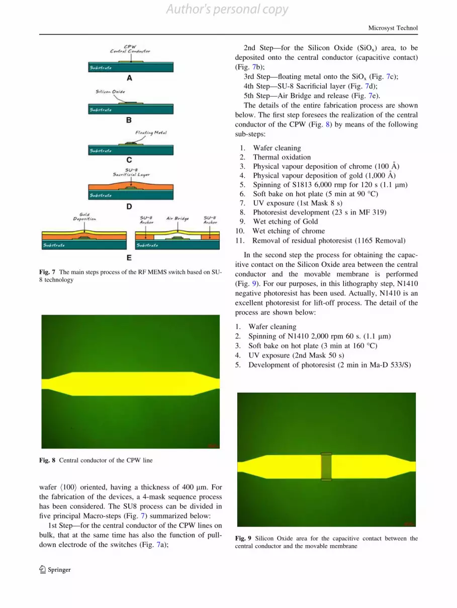
five principal Macro-steps (Fig. 7) summarized below:
1st Step—for the central conductor of the CPW lines on
bulk, that at the same time has also the function of pull-
down electrode of the switches (Fig. 7a);
2nd Step—for the Silicon Oxide (SiOx) area, to be
deposited onto the central conductor (capacitive contact)
(Fig. 7b);
3rd Step—floating metal onto the SiOx (Fig. 7c);
4th Step—SU-8 Sacrificial layer (Fig. 7d);
5th Step—Air Bridge and release (Fig. 7e).
The details of the entire fabrication process are shown
below. The first step foresees the realization of the central
conductor of the CPW (Fig. 8) by means of the following
sub-steps:
1. Wafer cleaning
2. Thermal oxidation
3. Physical vapour deposition of chrome (100 A)
4. Physical vapour deposition of gold (1,000 A)
5. Spinning of S1813 6,000 rmp for 120 s (1.1 lm)
6. Soft bake on hot plate (5 min at 90 �C)
7. UV exposure (1st Mask 8 s)
8. Photoresist development (23 s in MF 319)
9. Wet etching of Gold
10. Wet etching of chrome
11. Removal of residual photoresist (1165 Removal)
In the second step the process for obtaining the capac-
itive contact on the Silicon Oxide area between the central
conductor and the movable membrane is performed
(Fig. 9). For our purposes, in this lithography step, N1410
negative photoresist has been used. Actually, N1410 is an
excellent photoresist for lift-off process. The detail of the
process are shown below:
1. Wafer cleaning
2. Spinning of N1410 2,000 rpm 60 s. (1.1 lm)
3. Soft bake on hot plate (3 min at 160 �C)
4. UV exposure (2nd Mask 50 s)
5. Development of photoresist (2 min in Ma-D 533/S)
Fig. 7 The main steps process of the RF MEMS switch based on SU-
8 technology
Fig. 9 Silicon Oxide area for the capacitive contact between the
central conductor and the movable membrane
Fig. 8 Central conductor of the CPW line
Microsyst Technol
123
Author's personal copy

6. Thermal evaporation of chrome (Electron Gun 100 A)
7. Thermal evaporation of SiO2 (Electron Gun 2,500 A)
8. Lift off in acetone
The third step foresees the realization of the Floating
Metal area onto the Silicon Oxide for the uniformity of the
capacitive contact between the central conductor and the
movable membrane (Fig. 10). The fabrication process is
the same of the second step seen previously the only things
that changes are the mask and the deposited materials in this
(a bilayer of chrome and gold by PVD). Also in this case for
the lift off process is used N1410 negative photoresist. The
process details are the following:
1. Spinning of N1410 2,000 rpm 60 s. (1.1 lm)
2. Soft bake on hot plate (3 min at 160 �C)
3. UV exposure (3rd Mask 50 s)
4. Development of photoresist (2 min in Ma-D 533/S)
5. Rinse and dry
6. Thermal evaporation of chrome (Electron Gun 100 A)
7. Thermal evaporation of gold (Joule Effect 1,000 A)
8. Lift off in acetone
9. Rinse and dry
The fourth step foresees the realization of the SU-8
sacrificial layer and the lateral supports (Fig. 11). This step
is simple to be understood but, at the same time, is delicate
to be treated from a fabrication process point of view.
Actually, a thick layer of SU-8 negative photoresist is spin
coated and processed until hard bake (HB). The photoli-
thographic step does not require a mask because no
geometries have to be transferred onto the wafer but what
is done is a full exposure of the entire wafer creating in this
way at the same time the lateral supports and the sacrificial
layer. Attention has to be payed to the process of SU-8 in
order to avoid internal stress or crack of the polymer. The
details are given below:
1. Wafer cleaning
2. Spinning of SU-8 2002 800 rpm for 30 s (3 lm)
3. Ramped soft bake (from 22 to 95 �C with a raise
temperature of 2 �C/min)
4. UV exposure (Full Exposure 10 s)
5. Ramped post bake (PB) (from 22 to 95 �C with a raise
temperature of 2 �C/min)
6. Ramped HB (from 22 to 220 �C with a raise temper-
ature of 5 �C/min)
7. Hold HB at 220 �C for 30 min and cool down (SU-8
Sacrificial Layer)
The fifth and last step foresees the realization of the air
bridge (Fig. 12). In this step process after the deposition of
the seed layer composed by a three layer of metal (Cr/Au/
Cr) 1.5 lm of electroplating gold is grown onto the wafer
forming the ground planes and the air bridge. The details
are the following:
Fig. 10 Floating metal area onto the silicon oxide Fig. 11 SU-8 sacrificial layer and lateral supports
Fig. 12 RF MEMS switch based on SU-8 technology
Microsyst Technol
123
Author's personal copy

1. Wafer cleaning
2. PVD of chrome/gold (100 A/1,000 A)
3. Spinning of S1818 1,800 rmp for 30 s (2.8 lm)
4. SB on hot plate (5 min at 90 �C)
5. UV exposure (4th Mask 10 s)
6. Pre-development of photoresist
7. Development of photoresist (50 s MF 319)
8. Electrodeposition of gold (1.5 lm)
9. Photoresist removal (1165 Removal)
10. Wet etching of chrome seed layer
11. Wet etching of gold layer
12. Asher O2 (Release of the structure 15 min at 220 �C)
4 RF MEMS switch preliminary RF tests
Preliminary RF tests on the manufactured switches have
been performed and they are presented from Figs. 14, 15, 16.
The RF test bench is composed by the following instruments
(Fig. 13). This measurement set-up allows to measure the
S-parameters of the switches in ON and OFF state:
• Dual power supply
• 1 PC
• 1 VNA
• 1 Waveform generator
• 2 Digital multimeters
• 1 Temperature-relative humidity sensor
A Voltmeter (Hp3478 Digital Multimeter2) is in parallel
between the S pads and the GND pad to check the real
voltage and a current meter (Hp3478 Digital Multimeter1)
is in line to check the amount of current flowing in the
system. The DUT is kept under nitrogen flow and the test
conditions are:
• Temperature = 23/24 �C; RH & 30 %
• RF: SOLT Calibration from 45 MHz to 40 GHz, Power
3 dBm, # points 801
• Multi-meter resolution: Current 1 lA, Voltage 1 lV
The measured electrical performances are in good
agreement with the performed simulations. Actuation volt-
ages in the order of 20 volt have been imposed for the metal
Fig. 13 RF test set-up
Microsyst Technol
123
Author's personal copy

beam collapse, confirming the mechanical evaluations.
In particular, the devices have been designed to have the
best capacitance ON/OFF ratio around 10 GHz, and 0.5 dB
of insertion loss (Fig. 15), whereas 20 dB of return loss
(Fig. 14) have been obtained up to 10 GHz for the ON
(UP) state of the bridge, while an Isolation better than
25 dB has been measured at the frequency of resonance in
the OFF (DOWN) state (Fig. 16).
5 Conclusion
The realization of double-clamped RF MEMS capacitive
shunt switches in coplanar configuration by means of SU-8
technology has been proposed. In particular, cross-linked
negative photo-resist SU-8 has been used as a sacrificial
layer and, at the same time, as a pedestal to elevate the
ground planes of the CPW lines. RF MEMS switches
manufactured in this way present simplified technological
steps with respect to the usual technology based on other
kind of sacrificial materials, like SiO2 and positive photo-
resist materials. Preliminary RF tests on the manufactured
switches have been performed, and the measured electrical
performances are in good agreement with electromagnetic
simulations results.
References
Arscott S, Garet F, Mounaix P, Duvillaret L, Coutaz JL, Lippens D
(1999) Terahertz time-domain spectroscopy of films fabricated
from SU-8. Electron Lett 35:243–244. doi:10.1049/el:19990146
Bartolucci G, Catoni S, Giacomozzi F, Marcelli R, Margesin B,
Pochesci D (2007) Realisation of distributed RF MEMS phase
shifter with very low number of switches. Electron Lett
43:1290–1292. doi:10.1049/el:20071679
Bartolucci G, De Angelis G, Lucibello A, Marcelli R, Proietti E
(2012) Analytic modeling of RF MEMS shunt connected
capacitive switches. J Electromagn Waves Appl 26:1168–1179.
doi:10.1080/09205071.2012.710564
Brown ER (1998) RF-MEMS switches for reconfigurable integrated
circuits. IEEE Trans Microw Theory Tech 46:1868–1880. doi:
10.1109/22.734501
Bustillo JM, Howe RT, Muller RS (1998) Surface micromachining
for microelectromechanical systems. Proc IEEE 86:1552–1574.
doi:10.1109/5.704260
Cetiner B, Qian J, Chang H, Bachman M, Li G, De Flaviis F (2003)
Monolithic integration of RF MEMS switches with a diversity
antenna on PCB substrate. IEEE Trans Microw Theory Tech
51:332–335. doi:10.1109/TMTT.2002.806521
De Angelis G, Lucibello A, Proietti E, Marcelli R, Bartolucci G
(2012) Design and technology of micro-machined coplanar
grounded wave-guides. IET Microw Antennas Propag 6:497–504.
doi:10.1049/iet-map.2011.0240
Di Nardo S, Farinelli P, Giacomozzi F, Mannocchi G, Marcelli R,
Margesin B, Mezzanotte P, Mulloni V, Russer P, Sorrentino R,
Vitulli F, Vietzorreck L (2006) Broadband RF-MEMS based
SPDT. In: Proceedings 36th EuMC, Manchester, pp 501–504.
doi:10.1109/EMICC.2006.282693
MEMSCYCLOPEDIA, Free MEMS Encyclopedia (since 01/1999)
SU-8: Thick Photo-Resist for MEMS [online] (updated 10/2012).
http://memscyclopedia.org/su8.html. Accessed 9 Jan 2013
Fig. 14 Comparison between expected and measured transmission
parameters (reflection and transmission)
Fig. 15 Comparison between expected and measured insertion loss
(detail)
Fig. 16 Comparison between expected and measured isolation
parameters
Microsyst Technol
123
Author's personal copy

Kang S, Kim HC, Chun K (2008) Single pole four throw RF MEMS
switch with double stop comb drive. In: Proceedings Micro
Electro Mechanical Systems International Conference, Tucson,
pp 1036–1039. doi: 10.1109/MEMSYS.2008.4443836
Kovacs GTA, Maluf NI, Petersen KE (1998) Bulk micromachining of
silicon. Proc IEEE 86:1536–1551. doi:10.1109/5.704259
Lee J, Je CH, Kang S, Choi CA (2005) A low-loss single-pole six-
throw switch based on compact RF MEMS switches. IEEE Trans
Microw Theory Tech 53:3335–3344. doi:10.1109/TMTT.2005.
855746
Liu AQ, Palei W, Tang M, Alphones A (2004) Single-pole-four-throw
switch using high-aspect-ratio lateral switches. Electron Lett
40:1125–1126. doi:10.1049/el:20045718
Lucibello A, De Angelis G, Maiani M, Proietti E, Marcelli R (2009)
SU-8 based processes for the realization of RF MEMS structures.
In: Proceedings 10th International Symposium on RF MEMS
and RF Microsystems, Povo, Trento, Italy, pp 93–96
Malek CK, Saile V (2004) Applications of LIGA technology to
precision manufacturing of high-aspect-ratio micro components
and systems: a review. Microelectron J 35:131–143. doi:10.1016/
j.mejo.2003.10.003
Marcelli R, Catoni S, Frenguelli L (2008) Low-loss microwave
interconnections by using polymeric based coplanar waveguides
on low resistivity silicon substrates. Microelectron Eng 85:
425–431. doi:10.1016/j.mee.2007.08.002
Muldavin J, Bozler C, Keast C (2006) Wafer-scale packaged RF-
MEMS switches. In: Proceedings IEEE MTT-S International
Microwave Symposium, San Francisco, pp 267–270. doi:
10.1109/
MWSYM.2006.249484
Pilz D, Strohm KM, Luy JF (2000) SIMMWIC MEMS 180� switched
line phase shifter. In: Proceedings Silicon Monolithic Integrated
Circuits in RF Systems, Garmisch, pp 113–115. doi:10.1109/SM
IC.2000.844311
Rebeiz GM (2003) RF MEMS theory, design, and technology. Wiley,
New Jersey
Rebeiz GM, Tan GL, Hayden JS (2002) RF MEMS phase shifters:
design and applications. IEEE Microw Mag 3:72–81. doi:10.
1109/MMW.2002.1004054
Reuter SD, Bertz A, Schwenzer G, Gessner T (2005) Selective
adhesive bonding with SU-8 for zero-level-packaging. In: Chiao
J-C, Jamieson, DN, Faraone L, Dzurak AS (eds) Micro- and
nanotechnology: materials, processes, packaging, and systems II.
Proceedings of the SPIE, vol 5650. pp 163–171. doi:10.1117/12.
581829
Tan GL, Mihailovich RE, Hacker JB, DeNatale JF, Rebeiz GM
(2003) Low loss 2- and 4-bit TTD MEMS phase shifters based
on SP4T switches. IEEE Trans Microw Theory Tech 51:297–304.
doi:10.1109/TMTT.2002.806509
Microsyst Technol
123
Author's personal copy
Related Documents