•1 RF/Microwave Circuits I VNA Calibration Fall 2007 VNA & Calibration Vector Network Analyzer → Measures amplitude and phase of Reference, reflected, and transmitted signal to find [S] Basic Components of VNA Synthesized swept signal RF source Test set (signal routing from/to source, DUT, and internal IF circuitry) IF circuitry (down convert RF to IF, e.g., 100KHz) (page 183, 3 rd edition) Digital processors (A/D conversion, amp & phase measurements, etc)

Welcome message from author
This document is posted to help you gain knowledge. Please leave a comment to let me know what you think about it! Share it to your friends and learn new things together.
Transcript

•1
RF/Microwave Circuits I
VNA CalibrationFall 2007
VNA & Calibration
Vector Network Analyzer → Measures amplitude and phase of Reference, reflected, and transmitted signal to find [S]
Basic Components of VNA Synthesized swept signal RF source Test set (signal routing from/to source, DUT, and internal IF circuitry) IF circuitry (down convert RF to IF, e.g., 100KHz) (page 183, 3rd edition) Digital processors (A/D conversion, amp & phase measurements, etc)
•2
From Anritsu

•3
In reality, there is much hardware within VNA that affects a1, b1, etc Measurements are determined after IF and digital processing
∴ To determine [S] of the DUT, we need information about signals at DUT ports →have to calibrate/remove all VNA effects
Source [S]
DUT
Load
VNA VNA
measure a1, b1
measure a2, b2
[S] → scattering matrix [T] → transmission matrix (e.g., [ABCD]) Error box – networks that include internal VNA effects (couplers, switches, IF and
DSP circuits, etc) and possibly external cables etc different “error models” have different “error boxes”
First step: Determine how to represent these complex VNA effects. This is “error modeling”
•4
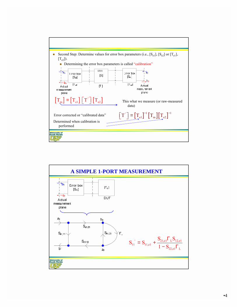
Second Step: Determine values for error box parameters (i.e., [Se1], [Se2] or [Te1], [Te2]). Determining the error box parameters is called “calibration”
[ ] [ ] [ ]'m e1 e2T T T T = This what we measure (or raw-measured
data)
Error corrected or “calibrated data” [ ] [ ][ ]1 1'e1 m e2T T T T− −
= Determined when calibration is
performed
A SIMPLE 1-PORT MEASUREMENT
Γ= +
− Γ21,e1 L 12,e1'
11 11,e122,e1 L
S SS S
1 S
•5
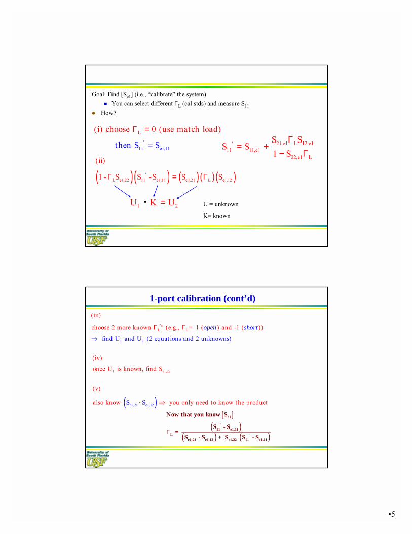
Goal: Find [Se1] (i.e., “calibrate” the system) You can select different ΓL (cal stds) and measure S11
How?
Γ
=
=L
'11 e1,11
(i) choose 0 (use match load)
then S S
( ) ( ) ( ) ( ) ( )Γ = Γ'L e1,22 11 e1,11 e1,21 L e1,12
(ii)
1 - S S -S S S
=1 2U K U U = unknown
K= known
Γ= +
− Γ21,e1 L 12,e1'
11 11,e122,e1 L
S SS S
1 S
.
1-port calibration (cont’d)
Γ
⇒
Γ'
1 2
sL L
(iii)
choose 2 more known (e.g., = 1 ( ) and -1
find U and U (2 equat ions and 2 unknow
)
ns)
( )open short
1 e1,22
(iv)
once U is known, find S
( ) ⇒e1,21 e1,12
(v)
also know you only need to know the proS S duct
[ ]( )
( ) ( )Γ
e1
'11 e1,11
L 'e1,21 e1,12 e1,22 11 e1,11
Now that you know S
S - S=
S - S + S S - S
·

•6
Commonly Used Calibration Methods
1. OSL (can be used only for 1-port calibration) Open, Short, Load
2. OSLT (2-port calibration) Open, Short, Load, Thru
– Thru is a section of matched transmission line
3. LRM Thru Line, Reflect, Matched load
– Reflect can be open or short
4. TRL Thru line, Reflect, delay Line
Commonly Used Calibration Methods
For many calibration methods, precise knowledge of the standards (e.g., the Γ for the short) must be known It won’t be exactly -1!

•7
TRL Calibration
Used for planar circuits (e.g., microstrip) this is the most accurate approach, especially at mm-wave frequencies
Does not require perfect (or well known) matched loads, opens, or sorts (other methods do require) ⇒ TRL is known as “self-calibrating”
How to construct TRL calibration lines for measuring a DUT…
TRL Calibration
To cables , VNA
To cables , VNA
L/ 2 L/ 2
Assumed to be identical in all measurements
THRUZ0
L/ 2 L/ 2
Z0 Z0
∆L
Z0
T.L (coax , microstrip , CPW , etc .)
DELAY
L/ 2 L/ 2
Z0 Z0
Γ1 Γ2
REFLECT
Reference plane in the center of thru

•8
TO MEASURE DUT
Z0 must be identical for all standards and DUT Theoretically, any L > 0 is acceptable Ideally, ∆L = 90° at center frequency
Calibration is typically valid from f1 to f2, when f1 when ∆L =20° f2 when ∆L =160°
Reflect standards do not have to be perfect opens or shorts, but Γ1 has to be identical to Γ2
Z0 does not have to be 50Ω, but its value does serve as the reference impedance for the calculated [S] matrix
DESIGN RULES
DESIGN TRL STD’s FROM 1-6GHz AND MEASURE A CHIP CAPACITOR
We need to know the following: Capacitor size, substrate properties on which capacitor will be
mounted/measured, what kind of TL (microstrip, CPW, etc) Frequency range
Capacitor dimensions from the manufacturer data sheet is 2mm × 1.2mm Given that the substrate is 31-mil FR-4 (εr=4.27)
Choose a value of “L”, this is the length of “thru”. There is no equation for choosing L Let’s say L=5mm
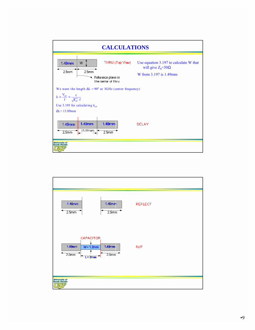
•9
CALCULATIONS
Use equation 3.197 to calculate W that will give Z0=50Ω
W from 3.197 is 1.49mm
ph
eff
eff
We want the length L = 90 at 3GHz (center frequency)
V cf f
Use 3.195 for calculat ing
L= 13.89mm
∆ °
λ = =ε
ε
∆

•10
TRL Standards and Test Fixtures
LineCalc

•11
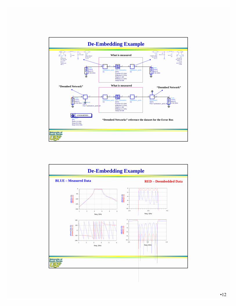
De-Embedding Example
S_ParamSP1
Step=0.01 GHzStop=6.0 GHzStart=1.0 GHz
S-PARAMETERS
TermTerm2
Z=50 OhmNum=2
TermTerm1
Z=50 OhmNum=1
PortP2Num=2
PortP1Num=1
COAXTL1
Rho=1TanD=0.002Er=2.1L=.1 meterDo=131.0 milDi=36.0 mil
MSUBMSub1
Rough=0 milTanD=0.02T=1 milHu=3.9e+034 milCond=1.0E+50Mur=1Er=9.6H=10.0 mil
MSubDisplayTemplatedisptemp1"S_Params_Quad_dB_Smith"
TempDisp
MLINTL2
L=2 cmW=10.0 milSubst="MSub1"
CC1C=1.0 pF
LL1
R=L=1.0 nH
Hypothetical Error Box Coax cable Connector Microstrip on circuit board
De-Embedding Example
freq (1.000GHz to 6.000GHz)
S(1
,1)
Input Reflection Coefficient
1.5 2.0 2.5 3.0 3.5 4.0 4.5 5.0 5.51.0 6.0
-150
-100
-50
0
50
100
150
-200
200
freq, GHz
pha
se(S
(2,1
))
Forward Transmission, dB
1.5 2.0 2.5 3.0 3.5 4.0 4.5 5.0 5.51.0 6.0
-3.0
-2.5
-2.0
-1.5
-1.0
-0.5
-3.5
0.0
freq, GHz
dB(S
(1,2
))
Reverse Transmission, dB
Use with S-Parameter Simulations
2 3 4 51 6
-18
-16
-14
-12
-10
-8
-6
-4
-20
-2
freq, GHz
dB(S
(1,1
))
Output Reflection Coefficient
S-parameters for the Error Box
•12
De-Embedding Example
S_ParamSP1
Step=0.01 GHzStop=6.0 GHzStart=1.0 GHz
S-PARAMETERS
1
1
2
TermTerm3
Z=50 OhmNum=3
1
1
2
TermTerm4
Z=50 OhmNum=4
21
BPF_ChebyshevBPF1
Astop=20 dBBWstop=1.2 GHzRipple=1 dBBWpass=1.0 GHzFcenter=3.5 GHz
12
cal ibration_port1X2
1 2
calibration_port1X1
12
cal ibration_port1X4
1 2
calibration_port1X3
1
2
TermTerm2
Z=50 OhmNum=2
1
12
3
Deembed2SNP2Fi le="cal ibration_port1.ds"
2 1
Re f
1
1
2
TermTerm1
Z=50 OhmNum=1
1
1
1 2
3
Deembed2SNP1Fi le="cal ibration_port1.ds"
21
Ref
21
BPF_ChebyshevBPF2
Astop=20 dBBWstop=1.2 GHzRipple=1 dBBWpass=1.0 GHzFcenter=3.5 GHz
COAXTL1
Rho=1TanD=0.002Er=2.1L=.1 meterDo=131.0 milDi=36.0 mil
MLINTL2
L=2 cmW=10.0 milSubst="MSub1"
CC1C=1.0 pF
LL1
R=L=1.0 nH COAX
TL1
Rho=1TanD=0.002Er=2.1L=.1 meterDo=131.0 milDi=36.0 mil
MLINTL2
L=2 cmW=10.0 milSubst="MSub1"
CC1C=1.0 pF
LL1
R=L=1.0 nHWhat is measured
What is measured“Deembed Network” “Deembed Network”
“Deembed Networks” reference the dataset for the Error Box
De-Embedding Example
2 3 4 51 6
-150
-100
-50
-200
0
freq, GHz
dB
(S(2
,1))
dB
(S(4
,3))
3.52.5 4.5
-8
-6
-4
-2
-10
0
freq, GHz
dB(S
(2,1
))dB
(S(4
,3))
2 3 4 51 6
-100
0
100
-200
200
freq, GHz
pha
se(S
(2,1
))p
ha
se(S
(4,3
))
3.52.5 4.5
-8
-6
-4
-2
-10
0
freq, GHz
dB
(S(1
,1))
dB
(S(3
,3))
BLUE – Measured Data RED – Deembedded Data
Related Documents