GaN Wideband Transistor 28 V, 45 W DC - 3.5 GHz Rev. V2 NPT1015B M/A-COM Technology Solutions Inc. (MACOM) and its affiliates reserve the right to make changes to the product(s) or information contained herein without notice. Visit www.macom.com for additional data sheets and product information. For further information and support please visit: https://www.macom.com/support 1 * Restrictions on Hazardous Substances, European Union Directive 2011/65/EU. Ordering Information Part Number Package NPT1015B bulk quantity NPT1015B-SMBPPR sample Features GaN on Si HEMT D-Mode Transistor Suitable for linear and saturated applications Tunable from DC - 3.5 GHz 28 V Operation 12 dB Gain @ 2.5 GHz 54 % Drain Efficiency @ 2.5 GHz 100 % RF Tested Standard metal ceramic package with bolt down flange RoHS* Compliant Description The NPT1015 GaN HEMT is a wideband transistor optimized for DC - 3.5 GHz operation. This device supports CW, pulsed, and linear operation with output power levels to 45 W (46.5 dBm) in an industry standard metal-ceramic package with bolt down flange. The NPT1015 is ideally suited for defense communications, land mobile radio, avionics, wireless infrastructure, ISM applications and VHF/ UHF/L/S-band radar. Built using the SIGANTIC® process - a proprietary GaN-on-Silicon technology. Pin Configuration Functional Schematic Pin No. Pin Name Function 1 RF IN / V G RF Input / Gate 2 RF OUT / V D RF Output / Drain 3 Flange 1 Ground / Source 1. The Flange must be connected to RF and DC ground. This path must also provide a low thermal resistance heat path. RF OUT / V D RF IN / V G Flange 3 1 2

Welcome message from author
This document is posted to help you gain knowledge. Please leave a comment to let me know what you think about it! Share it to your friends and learn new things together.
Transcript

GaN Wideband Transistor 28 V, 45 W DC - 3.5 GHz
Rev. V2
NPT1015B
1 1
M/A-COM Technology Solutions Inc. (MACOM) and its affiliates reserve the right to make changes to the product(s) or information contained herein without notice. Visit www.macom.com for additional data sheets and product information.
For further information and support please visit: https://www.macom.com/support
1
* Restrictions on Hazardous Substances, European Union Directive 2011/65/EU.
Ordering Information
Part Number Package
NPT1015B bulk quantity
NPT1015B-SMBPPR sample
Features
GaN on Si HEMT D-Mode Transistor
Suitable for linear and saturated applications
Tunable from DC - 3.5 GHz
28 V Operation
12 dB Gain @ 2.5 GHz
54 % Drain Efficiency @ 2.5 GHz
100 % RF Tested
Standard metal ceramic package with bolt down flange
RoHS* Compliant
Description
The NPT1015 GaN HEMT is a wideband transistor optimized for DC - 3.5 GHz operation. This device supports CW, pulsed, and linear operation with output power levels to 45 W (46.5 dBm) in an industry standard metal-ceramic package with bolt down flange. The NPT1015 is ideally suited for defense communications, land mobile radio, avionics, wireless infrastructure, ISM applications and VHF/UHF/L/S-band radar. Built using the SIGANTIC® process - a proprietary GaN-on-Silicon technology.
Pin Configuration
Functional Schematic
Pin No. Pin Name Function
1 RFIN / VG RF Input / Gate
2 RFOUT / VD RF Output / Drain
3 Flange1 Ground / Source
1. The Flange must be connected to RF and DC ground. This path must also provide a low thermal resistance heat path.
RFOUT / VDRFIN / VG
Flange
3
1 2
GaN Wideband Transistor 28 V, 45 W DC - 3.5 GHz
Rev. V2
NPT1015B
2 2
M/A-COM Technology Solutions Inc. (MACOM) and its affiliates reserve the right to make changes to the product(s) or information contained herein without notice. Visit www.macom.com for additional data sheets and product information.
For further information and support please visit: https://www.macom.com/support
2
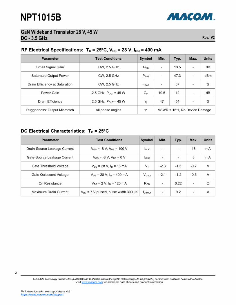
RF Electrical Specifications: TC = 25C, VDS = 28 V, IDQ = 400 mA
Parameter Test Conditions Symbol Min. Typ. Max. Units
Small Signal Gain CW, 2.5 GHz GSS - 13.5 - dB
Saturated Output Power CW, 2.5 GHz PSAT - 47.3 - dBm
Drain Efficiency at Saturation CW, 2.5 GHz SAT - 57 - %
Power Gain 2.5 GHz, POUT = 45 W GP 10.5 12 - dB
Drain Efficiency 2.5 GHz, POUT = 45 W 47 54 - %
Ruggedness: Output Mismatch All phase angles VSWR = 15:1, No Device Damage
DC Electrical Characteristics: TC = 25C
Parameter Test Conditions Symbol Min. Typ. Max. Units
Drain-Source Leakage Current VGS = -8 V, VDS = 100 V IDLK - - 16 mA
Gate-Source Leakage Current VGS = -8 V, VDS = 0 V IGLK - - 8 mA
Gate Threshold Voltage VDS = 28 V, ID = 16 mA VT -2.3 -1.5 -0.7 V
Gate Quiescent Voltage VDS = 28 V, ID = 400 mA VGSQ -2.1 -1.2 -0.5 V
On Resistance VDS = 2 V, ID = 120 mA RON - 0.22 -
Maximum Drain Current VDS = 7 V pulsed, pulse width 300 µs ID,MAX - 9.2 - A

GaN Wideband Transistor 28 V, 45 W DC - 3.5 GHz
Rev. V2
NPT1015B
3 3
M/A-COM Technology Solutions Inc. (MACOM) and its affiliates reserve the right to make changes to the product(s) or information contained herein without notice. Visit www.macom.com for additional data sheets and product information.
For further information and support please visit: https://www.macom.com/support
3
Absolute Maximum Ratings2,3,4
2. Exceeding any one or combination of these limits may cause permanent damage to this device. 3. MACOM does not recommend sustained operation near these survivability limits. 4. Operating at nominal conditions with TJ ≤ 200°C will ensure MTTF > 1 x 10⁶ hours.
Parameter Absolute Maximum
Drain Source Voltage, VDS 100 V
Gate Source Voltage, VGS -10 to 3 V
Gate Current, IG 32 mA
Junction Temperature, TJ +200°C
Operating Temperature -40°C to +85°C
Storage Temperature -65°C to +150°C
5. Junction temperature (TJ) measured using IR Microscopy. Case temperature measured using thermocouple embedded in heat-sink.
Parameter Test Conditions Symbol Typical Units
Thermal Resistance VDS = 28 V, TJ = 180°C RJC 2.1 °C/W
Thermal Characteristics5
Handling Procedures
Please observe the following precautions to avoid damage:
Static Sensitivity
Gallium Nitride Circuits are sensitive to electrostatic discharge (ESD) and can be damaged by static electricity. Proper ESD control techniques should be used when handling these HBM Class 1B devices.

GaN Wideband Transistor 28 V, 45 W DC - 3.5 GHz
Rev. V2
NPT1015B
4 4
M/A-COM Technology Solutions Inc. (MACOM) and its affiliates reserve the right to make changes to the product(s) or information contained herein without notice. Visit www.macom.com for additional data sheets and product information.
For further information and support please visit: https://www.macom.com/support
4
Frequency (MHz)
ZS
()
ZL
()
PSAT (W)
GSS (dB)
Drain Efficiency @ PSAT (%)
900 1.1 + j0.7 6.3 + j1.8 53.7 22.5 65.1
2200 1.6 - j6.0 5.4 - j0.6 53.2 15.8 64.8
2500 1.5 - j6.7 5.2 - j2.2 50.9 15.0 60.8
3500 2.6 - j15 3.9 - j6.3 42.0 13.9 55.4
Load-Pull Performance: VDS = 28 V, IDQ = 400 mA, TC = 25°C
Reference Plane at Device Leads, CW Drain Efficiency and Output Power Tradeoff Impedance
Gain vs. Output Power Drain Efficiency vs. Output Power
Impedance Reference ZS and ZL vs. Frequency
ZS ZL
10
12
14
16
18
20
22
24
25 30 35 40 45 50
900MHz
2200MHz2500MHz
3500MHz
Gain
(d
B)
POUT (dBm)
0
10
20
30
40
50
60
70
25 30 35 40 45 50
900MHz
2200MHz
2500MHz3500MHz
Dra
in E
ffic
iency (
%)
POUT (dBm)

GaN Wideband Transistor 28 V, 45 W DC - 3.5 GHz
Rev. V2
NPT1015B
5 5
M/A-COM Technology Solutions Inc. (MACOM) and its affiliates reserve the right to make changes to the product(s) or information contained herein without notice. Visit www.macom.com for additional data sheets and product information.
For further information and support please visit: https://www.macom.com/support
5
Parts measured on evaluation board (20-mil thick RO4350). Matching is provided using a combination of lumped elements and transmission lines as shown in the simplified schematic above. Recommended tuning solution component placement, transmission lines, and details are shown on the next page.
Evaluation Board and Recommended Tuning Solution
2.5 GHz Narrowband Circuit
Description
Turning the device ON
1. Set VGS to the pinch-off (VP), typically -5 V. 2. Turn on VDS to nominal voltage (28 V). 3. Increase VGS until the IDS current is reached. 4. Apply RF power to desired level.
Turning the device OFF
1. Turn the RF power off. 2. Decrease VGS down to VP. 3. Decrease VDS down to 0 V. 4. Turn off VGS.
Bias Sequencing
L119.4 nH
R1
15
C1310 pF
RFIN
C41000 pF
C3
0.01 mF
C2
0.1 mF
C1
1.0 mF
VGS VDS
C150.6 pF
C1410 pF
RFOUT
C910 pF
NPT1015
C5
1.0 mFC6
0.1 mF
C7
0.01 mFC81000pF
C122.2 pF
C112.4 pF
C1020 pF

GaN Wideband Transistor 28 V, 45 W DC - 3.5 GHz
Rev. V2
NPT1015B
6 6
M/A-COM Technology Solutions Inc. (MACOM) and its affiliates reserve the right to make changes to the product(s) or information contained herein without notice. Visit www.macom.com for additional data sheets and product information.
For further information and support please visit: https://www.macom.com/support
6
Reference Value Tolerance Manufacturer Part Number
C1, C5 1.0 µF 10% AVX 12101C105KAT2A
C2, C6 0.1 µF 10% Kemet C1206C104K1RACTU
C3, C7 0.01 µF 10% AVX 1206C103KAT2A
C4, C8 1000 pF 10% Kemet C0805C102K1RACTU
C9, C14 10 pF 0.1 pF ATC ATC800B100B
C10 20 pF 0.1 pF ATC ATC800B200B
C11 2.4 pF 0.1 pF ATC ATC600F2R4B
C12 2.2 pF 0.1 pF ATC ATC600F2R2B
C13 10 pF 0.1 pF ATC ATC600F100B
C15 0.6 pF 0.1 pF ATC ATC600F0R6B
L1 19.4 nH 5% CoilCraft 0806SQ-19NJL
R1 15 Ω 1% Panasonic ERJ-2RKF15R0X
PCB Rogers RO4350, r = 3.5, 0.020”
Parts list
Evaluation Board and Recommended Tuning Solution
2.5 GHz Narrowband Circuit
GaN Wideband Transistor 28 V, 45 W DC - 3.5 GHz
Rev. V2
NPT1015B
7 7
M/A-COM Technology Solutions Inc. (MACOM) and its affiliates reserve the right to make changes to the product(s) or information contained herein without notice. Visit www.macom.com for additional data sheets and product information.
For further information and support please visit: https://www.macom.com/support
7
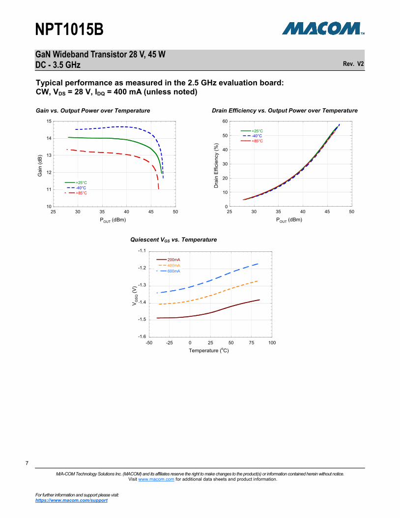
Typical performance as measured in the 2.5 GHz evaluation board: CW, VDS = 28 V, IDQ = 400 mA (unless noted)
Gain vs. Output Power over Temperature Drain Efficiency vs. Output Power over Temperature
Quiescent VGS vs. Temperature
0
10
20
30
40
50
60
25 30 35 40 45 50
+25°C
-40°C
+85°C
Dra
in E
ffic
iency (
%)
POUT (dBm)
-1.6
-1.5
-1.4
-1.3
-1.2
-1.1
-50 -25 0 25 50 75 100
200mA
400mA
600mA
VG
SQ (
V)
Temperature (oC)
10
11
12
13
14
15
25 30 35 40 45 50
+25°C
-40°C
+85°C
Gain
(d
B)
POUT (dBm)

GaN Wideband Transistor 28 V, 45 W DC - 3.5 GHz
Rev. V2
NPT1015B
8 8
M/A-COM Technology Solutions Inc. (MACOM) and its affiliates reserve the right to make changes to the product(s) or information contained herein without notice. Visit www.macom.com for additional data sheets and product information.
For further information and support please visit: https://www.macom.com/support
8
2-Tone IMD vs. Output Power
2-Tone IMD3 vs. Output Power vs. Quiescent Current 2-Tone Gain vs. Output Power vs. Quiescent Current
Typical 2-Tone Performance as measured in the 2.5 GHz evaluation board: 1 MHz Tone Spacing, VDS = 28 V, IDQ = 400 mA, TC = 25°C (unless noted)
-50
-45
-40
-35
-30
-25
-20
-15
0.1 1 10 100
200mA
300mA
400mA
600mA
800mA
IMD
(d
Bc)
POUT (W-PEP)
12.0
12.5
13.0
13.5
14.0
14.5
15.0
0.1 1 10 100
200mA
300mA
400mA
600mA
800mA
Gain
(d
B)
POUT (W-PEP)
-55
-50
-45
-40
-35
-30
-25
-20
0.1 1 10 100
-IMD3
+IMD3
-IMD5
+IMD5
-IMD7
+IMD7
IMD
(d
Bc)
POUT (W-PEP)

GaN Wideband Transistor 28 V, 45 W DC - 3.5 GHz
Rev. V2
NPT1015B
9 9
M/A-COM Technology Solutions Inc. (MACOM) and its affiliates reserve the right to make changes to the product(s) or information contained herein without notice. Visit www.macom.com for additional data sheets and product information.
For further information and support please visit: https://www.macom.com/support
9
Evaluation Board and Recommended Tuning Solution
600 - 1000 MHz Broadband Circuit
Reference Value Tolerance Manufacturer Part Number
C1 150 µF 20% Nichicon UPW1C151MED
C2, C5 0.01 µF 10% AVX 1206C103KAT2A
C3, C6 0.1 µF 10% Kemet C1206C104K1RACTU
C4, C7 1.0 µF 10% AVX 12101C105KAT2A
C8 270 µF 20% United Chemi-Con ELXY 630ELL271MK25S
C9 56 pF 5% ATC ATC100B560J
C10, C12 100 pF 5% ATC ATC100B101J
C11 6.8 pF 5% ATC ATC100B6R8J
R1, R2 0.33 Ω 1% Panasonic ERJ-6RQFR33V
R3 10 Ω 1% Panasonic ERJ-6ENF10R0V
R4, R5 7.5 Ω 1% Stackpole RHC2512FT7R50
L1 120 nH 5% Coilcraft 0805CS-121XJB
L2 ~50 nH - 16 AWG Cu Wire 5 turn, 0.2"ID
PCB Rogers LM6010, r = 10.2, 0.025”
Parts list

GaN Wideband Transistor 28 V, 45 W DC - 3.5 GHz
Rev. V2
NPT1015B
10 10
M/A-COM Technology Solutions Inc. (MACOM) and its affiliates reserve the right to make changes to the product(s) or information contained herein without notice. Visit www.macom.com for additional data sheets and product information.
For further information and support please visit: https://www.macom.com/support
10
Evaluation Board and Recommended Tuning Solution
600 - 1000 MHz Broadband Circuit
Performance vs. Frequency at POUT = PSAT Performance vs. Frequency at POUT = 45 dBm
Performance vs. Output Power (f = 700 MHz) Small Signal s-parameters vs. Frequency
5
10
15
20
25
40
50
60
70
80
600 700 800 900 1,000
Gain
Drain Eff
Psat
Gain
(d
B)
PS
AT (d
Bm
), Dra
in E
fficie
ncy (%
)
Frequency (MHz)
10
15
20
25
30
30
40
50
60
70
600 700 800 900 1,000
Gain
Drain Eff
Gain
(d
B)
Dra
in E
fficie
ncy (%
)
Frequency (MHz)
15
16
17
18
19
20
0
10
20
30
40
50
60
70
25 30 35 40 45 50
Gain
Drain Eff
Gain
(d
B)
Dra
in E
fficie
ncy (%
)
POUT (dBm)
R3
10
C1010 pF
RFIN
C956 pF
VG VD
C12100 pF
RFOUT
NPT1015
L28.0 nH
L1120 nH
R4
7.5
R5
7.5
C116.8 pF
C7
1.0 mFC6
0.1 mF
C5
0.01 mF
C8
270 mFR2
0.33
C4
1.0 mFC3
0.1 mF
C2
0.01 mF
C1
150 mF R1
0.33
10
15
20
25
30
35
-30
-25
-20
-15
-10
-5
500 600 700 800 900 1,000
s21
s11
s22
s2
1 (
dB
)
s1
1 , s2
2 (dB
)
Frequency (MHz)

GaN Wideband Transistor 28 V, 45 W DC - 3.5 GHz
Rev. V2
NPT1015B
11 11
M/A-COM Technology Solutions Inc. (MACOM) and its affiliates reserve the right to make changes to the product(s) or information contained herein without notice. Visit www.macom.com for additional data sheets and product information.
For further information and support please visit: https://www.macom.com/support
11
AC360B-2 Metal Ceramic Package†
† Plating is Ni / Au.
All dimensions shown as inches [millimeters].
GaN Wideband Transistor 28 V, 45 W DC - 3.5 GHz
Rev. V2
NPT1015B
12 12
M/A-COM Technology Solutions Inc. (MACOM) and its affiliates reserve the right to make changes to the product(s) or information contained herein without notice. Visit www.macom.com for additional data sheets and product information.
For further information and support please visit: https://www.macom.com/support
12
M/A-COM Technology Solutions Inc. All rights reserved. Information in this document is provided in connection with M/A-COM Technology Solutions Inc ("MACOM")products. These materials are provided by MACOM as a service to its customers and may be used for informational purposes only. Except as provided in MACOM's Terms and Conditions of Sale for such products or in any separate agreement related to this document, MACOM assumes no liability whatsoever. MACOM assumes no responsibility for errors or omissions in these materials. MACOM may make changes to specifications and product descriptions at any time, without notice. MACOM makes no commitment to update the information and shall have no responsibility whatsoever for conflicts or incompatibilities arising from future changes to its specifications and product descriptions. No license, express or implied, by estoppels or otherwise, to any intellectual property rights is granted by this document. THESE MATERIALS ARE PROVIDED "AS IS" WITHOUT WARRANTY OF ANY KIND, EITHER EXPRESS OR IMPLIED, RELATING TO SALE AND/OR USE OF MACOM PRODUCTS INCLUDING LIABILITY OR WARRANTIES RELATING TO FITNESS FOR A PARTICULAR PURPOSE, CONSEQUENTIAL OR INCIDENTAL DAMAGES, MERCHANTABILITY, OR INFRINGEMENT OF ANY PATENT, COPYRIGHT OR OTHER INTELLECTUAL PROPERTY RIGHT. MACOM FURTHER DOES NOT WARRANT THE ACCURACY OR COMPLETENESS OF THE INFORMATION, TEXT, GRAPHICS OR OTHER ITEMS CONTAINED WITHIN THESE MATERIALS. MACOM SHALL NOT BE LIABLE FOR ANY SPECIAL, INDIRECT, INCIDENTAL, OR CONSEQUENTIAL DAMAGES, INCLUDING WITHOUT LIMITATION, LOST REVENUES OR LOST PROFITS, WHICH MAY RESULT FROM THE USE OF THESE MATERIALS. MACOM products are not intended for use in medical, lifesaving or life sustaining applications. MACOM customers using or selling MACOM products for use in such applications do so at their own risk and agree to fully indemnify MACOM for any damages resulting from such improper use or sale.
Related Documents