RF Power LDMOS Transistors High Ruggedness N--Channel Enhancement--Mode Lateral MOSFETs These devices are designed for use in HF and VHF communications, industrial, scientific and medical (ISM) and broadcast and aerospace applications. The devices are extremely rugged and exhibit high performance up to 250 MHz. Typical Performance: V DD = 50 Vdc Frequency (MHz) Signal Type P out (W) G ps (dB) D (%) 13.56 (1) CW 130 CW 27.1 79.6 27 (2) CW 125 CW 24.9 79.6 40.68 (3) CW 120 CW 23.8 81.5 50 (4) CW 119 CW 22.8 82.1 81.36 (5) CW 130 CW 23.2 80.8 87.5–108 (6,7) CW 115 CW 20.6 76.8 136–174 (7,8) CW 104 CW 21.2 76.5 230 (9) Pulse (100 sec, 20% Duty Cycle) 115 Peak 21.1 76.7 Load Mismatch/Ruggedness Frequency (MHz) Signal Type VSWR P in (W) Test Voltage Result 40.68 CW > 65:1 at all Phase Angles 0.64 CW 50 No Device Degradation 230 Pulse (100 sec, 20% Duty Cycle) > 65:1 at all Phase Angles 1.8 Peak (3 dB Overdrive) 50 No Device Degradation 1. Measured in 13.56 MHz reference circuit (page 5). 2. Measured in 27 MHz reference circuit (page 9). 3. Measured in 40.68 MHz reference circuit (page 13). 4. Measured in 50 MHz reference circuit (page 17). 5. Measured in 81.36 MHz reference circuit (page 21). 6. Measured in 87.5–108 MHz broadband reference circuit (page 25). 7. The values shown are the center band performance numbers across the indicated frequency range. 8. Measured in 136–174 MHz VHF broadband reference circuit (page 30). 9. Measured in 230 MHz fixture (page 34). Features Mirror pinout versions (A and B) to simplify use in a push--pull, two--up configuration Characterized from 30 to 50 V Suitable for linear application Integrated ESD protection with greater negative gate--source voltage range for improved Class C operation Included in NXP product longevity program with assured supply for a minimum of 15 years after launch Typical Applications Industrial, scientific, medical (ISM) – Laser generation – Plasma etching – Particle accelerators – MRI and other medical applications – Industrial heating, welding and drying systems Radio and VHF TV broadcast HF and VHF communications Switch mode power supplies Document Number: MRF101AN Rev. 1, 05/2019 NXP Semiconductors Technical Data 1.8–250 MHz, 100 W CW, 50 V WIDEBAND RF POWER LDMOS TRANSISTORS MRF101AN MRF101BN TO--220--3 MRF101BN TO--220--3 MRF101AN G S D D S G Note: Exposed backside of the package and tab also serves as a source terminal for the transistor. Backside S S D S G 2018–2019 NXP B.V.

Welcome message from author
This document is posted to help you gain knowledge. Please leave a comment to let me know what you think about it! Share it to your friends and learn new things together.
Transcript
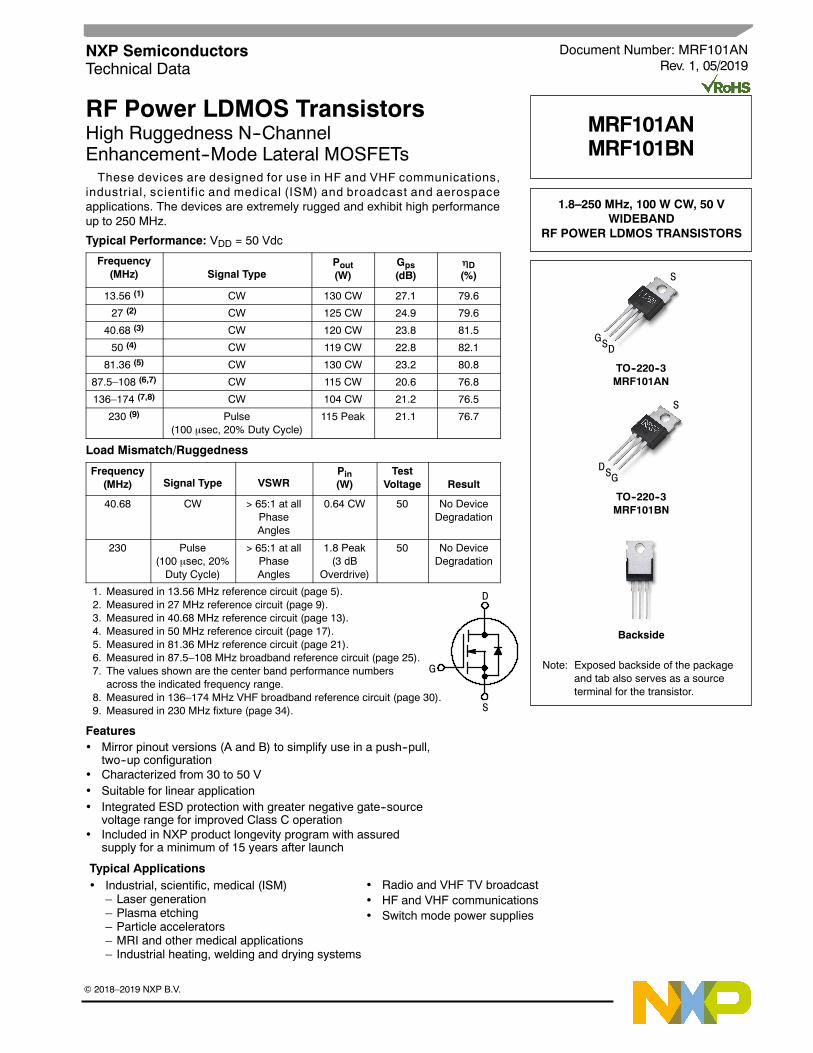
MRF101AN MRF101BN
1RF Device DataNXP Semiconductors
RF Power LDMOS TransistorsHigh Ruggedness N--ChannelEnhancement--Mode Lateral MOSFETsThese devices are designed for use in HF and VHF communications,
industrial, scientif ic and medical (ISM) and broadcast and aerospaceapplications. The devices are extremely rugged and exhibit high performanceup to 250 MHz.
Typical Performance: VDD = 50 Vdc
Frequency(MHz) Signal Type
Pout(W)
Gps(dB)
D(%)
13.56 (1) CW 130 CW 27.1 79.6
27 (2) CW 125 CW 24.9 79.6
40.68 (3) CW 120 CW 23.8 81.5
50 (4) CW 119 CW 22.8 82.1
81.36 (5) CW 130 CW 23.2 80.8
87.5–108 (6,7) CW 115 CW 20.6 76.8
136–174 (7,8) CW 104 CW 21.2 76.5
230 (9) Pulse(100 sec, 20% Duty Cycle)
115 Peak 21.1 76.7
Load Mismatch/Ruggedness
Frequency(MHz) Signal Type VSWR
Pin(W)
TestVoltage Result
40.68 CW > 65:1 at allPhaseAngles
0.64 CW 50 No DeviceDegradation
230 Pulse(100 sec, 20%Duty Cycle)
> 65:1 at allPhaseAngles
1.8 Peak(3 dB
Overdrive)
50 No DeviceDegradation
1. Measured in 13.56 MHz reference circuit (page 5).2. Measured in 27 MHz reference circuit (page 9).3. Measured in 40.68 MHz reference circuit (page 13).4. Measured in 50 MHz reference circuit (page 17).5. Measured in 81.36 MHz reference circuit (page 21).6. Measured in 87.5–108 MHz broadband reference circuit (page 25).7. The values shown are the center band performance numbers
across the indicated frequency range.8. Measured in 136–174 MHz VHF broadband reference circuit (page 30).9. Measured in 230 MHz fixture (page 34).
Features Mirror pinout versions (A and B) to simplify use in a push--pull,
two--up configuration Characterized from 30 to 50 V Suitable for linear application Integrated ESD protection with greater negative gate--source
voltage range for improved Class C operation Included in NXP product longevity program with assured
supply for a minimum of 15 years after launch
Typical Applications Industrial, scientific, medical (ISM)
– Laser generation– Plasma etching– Particle accelerators– MRI and other medical applications– Industrial heating, welding and drying systems
Radio and VHF TV broadcast HF and VHF communications Switch mode power supplies
Document Number: MRF101ANRev. 1, 05/2019
NXP SemiconductorsTechnical Data
1.8–250 MHz, 100 W CW, 50 VWIDEBAND
RF POWER LDMOS TRANSISTORS
MRF101ANMRF101BN
TO--220--3MRF101BN
TO--220--3MRF101AN
GSD
DSG
Note: Exposed backside of the packageand tab also serves as a sourceterminal for the transistor.
Backside
S
S
D
S
G
2018–2019 NXP B.V.
2RF Device Data
NXP Semiconductors
MRF101AN MRF101BN
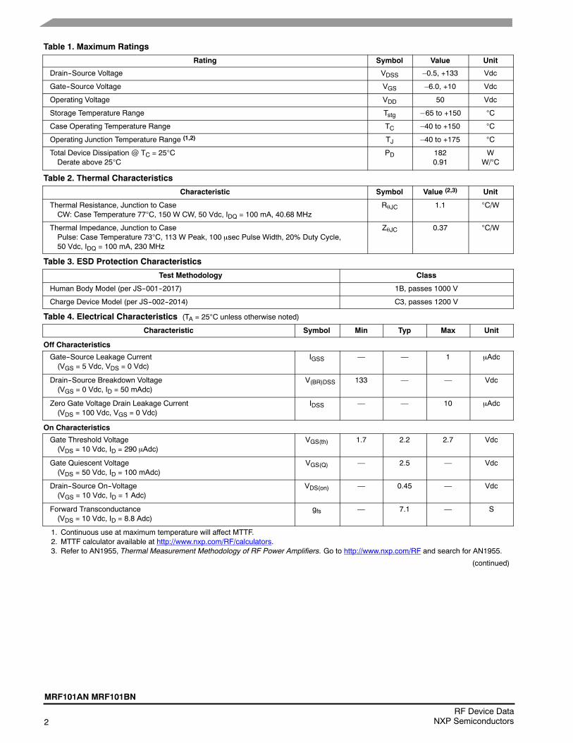
Table 1. Maximum Ratings
Rating Symbol Value Unit
Drain--Source Voltage VDSS –0.5, +133 Vdc
Gate--Source Voltage VGS –6.0, +10 Vdc
Operating Voltage VDD 50 Vdc
Storage Temperature Range Tstg –65 to +150 C
Case Operating Temperature Range TC –40 to +150 C
Operating Junction Temperature Range (1,2) TJ –40 to +175 C
Total Device Dissipation @ TC = 25CDerate above 25C
PD 1820.91
WW/C
Table 2. Thermal Characteristics
Characteristic Symbol Value (2,3) Unit
Thermal Resistance, Junction to CaseCW: Case Temperature 77C, 150 W CW, 50 Vdc, IDQ = 100 mA, 40.68 MHz
RJC 1.1 C/W
Thermal Impedance, Junction to CasePulse: Case Temperature 73C, 113 W Peak, 100 sec Pulse Width, 20% Duty Cycle,50 Vdc, IDQ = 100 mA, 230 MHz
ZJC 0.37 C/W
Table 3. ESD Protection Characteristics
Test Methodology Class
Human Body Model (per JS--001--2017) 1B, passes 1000 V
Charge Device Model (per JS--002--2014) C3, passes 1200 V
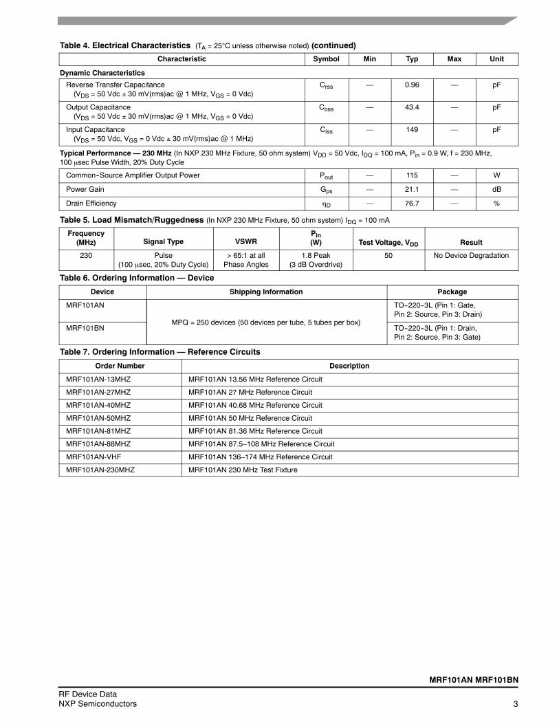
Table 4. Electrical Characteristics (TA = 25C unless otherwise noted)
Characteristic Symbol Min Typ Max Unit
Off Characteristics
Gate--Source Leakage Current(VGS = 5 Vdc, VDS = 0 Vdc)
IGSS — — 1 Adc
Drain--Source Breakdown Voltage(VGS = 0 Vdc, ID = 50 mAdc)
V(BR)DSS 133 — — Vdc
Zero Gate Voltage Drain Leakage Current(VDS = 100 Vdc, VGS = 0 Vdc)
IDSS — — 10 Adc
On Characteristics
Gate Threshold Voltage(VDS = 10 Vdc, ID = 290 Adc)
VGS(th) 1.7 2.2 2.7 Vdc
Gate Quiescent Voltage(VDS = 50 Vdc, ID = 100 mAdc)
VGS(Q) — 2.5 — Vdc
Drain--Source On--Voltage(VGS = 10 Vdc, ID = 1 Adc)
VDS(on) — 0.45 — Vdc
Forward Transconductance(VDS = 10 Vdc, ID = 8.8 Adc)
gfs — 7.1 — S
1. Continuous use at maximum temperature will affect MTTF.2. MTTF calculator available at http://www.nxp.com/RF/calculators.3. Refer to AN1955, Thermal Measurement Methodology of RF Power Amplifiers. Go to http://www.nxp.com/RF and search for AN1955.
(continued)
MRF101AN MRF101BN
3RF Device DataNXP Semiconductors
Table 4. Electrical Characteristics (TA = 25C unless otherwise noted) (continued)
Characteristic Symbol Min Typ Max Unit
Dynamic Characteristics
Reverse Transfer Capacitance(VDS = 50 Vdc 30 mV(rms)ac @ 1 MHz, VGS = 0 Vdc)
Crss — 0.96 — pF
Output Capacitance(VDS = 50 Vdc 30 mV(rms)ac @ 1 MHz, VGS = 0 Vdc)
Coss — 43.4 — pF
Input Capacitance(VDS = 50 Vdc, VGS = 0 Vdc 30 mV(rms)ac @ 1 MHz)
Ciss — 149 — pF
Typical Performance — 230 MHz (In NXP 230 MHz Fixture, 50 ohm system) VDD = 50 Vdc, IDQ = 100 mA, Pin = 0.9 W, f = 230 MHz,100 sec Pulse Width, 20% Duty Cycle
Common--Source Amplifier Output Power Pout — 115 — W
Power Gain Gps — 21.1 — dB
Drain Efficiency D — 76.7 — %
Table 5. Load Mismatch/Ruggedness (In NXP 230 MHz Fixture, 50 ohm system) IDQ = 100 mA
Frequency(MHz) Signal Type VSWR
Pin(W) Test Voltage, VDD Result
230 Pulse(100 sec, 20% Duty Cycle)
> 65:1 at allPhase Angles
1.8 Peak(3 dB Overdrive)
50 No Device Degradation
Table 6. Ordering Information — Device
Device Shipping Information Package
MRF101AN
MPQ = 250 devices (50 devices per tube, 5 tubes per box)
TO--220--3L (Pin 1: Gate,Pin 2: Source, Pin 3: Drain)
MRF101BN TO--220--3L (Pin 1: Drain,Pin 2: Source, Pin 3: Gate)
Table 7. Ordering Information — Reference Circuits
Order Number Description
MRF101AN-13MHZ MRF101AN 13.56 MHz Reference Circuit
MRF101AN-27MHZ MRF101AN 27 MHz Reference Circuit
MRF101AN-40MHZ MRF101AN 40.68 MHz Reference Circuit
MRF101AN-50MHZ MRF101AN 50 MHz Reference Circuit
MRF101AN-81MHZ MRF101AN 81.36 MHz Reference Circuit
MRF101AN-88MHZ MRF101AN 87.5–108 MHz Reference Circuit
MRF101AN-VHF MRF101AN 136–174 MHz Reference Circuit
MRF101AN-230MHZ MRF101AN 230 MHz Test Fixture
4RF Device Data
NXP Semiconductors
MRF101AN MRF101BN
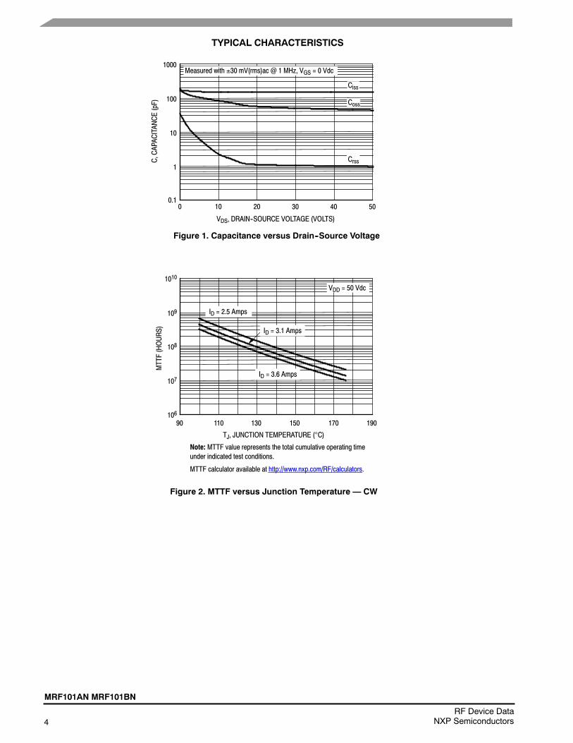
TYPICAL CHARACTERISTICS
1
100
0 2010
VDS, DRAIN--SOURCE VOLTAGE (VOLTS)
Figure 1. Capacitance versus Drain--Source Voltage
C,CAPACITANCE(pF)
10
Crss
Ciss
30 40 50
1000
Coss
Measured with 30 mV(rms)ac @ 1 MHz, VGS = 0 Vdc
0.1
1010
90
TJ, JUNCTION TEMPERATURE (C)
Figure 2. MTTF versus Junction Temperature — CW
Note: MTTF value represents the total cumulative operating timeunder indicated test conditions.
MTTF calculator available at http://www.nxp.com/RF/calculators.
108
107
110 130
MTTF(HOURS)
150
109
106170 190
ID = 2.5 Amps
VDD = 50 Vdc
ID = 3.6 Amps
ID = 3.1 Amps

MRF101AN MRF101BN
5RF Device DataNXP Semiconductors
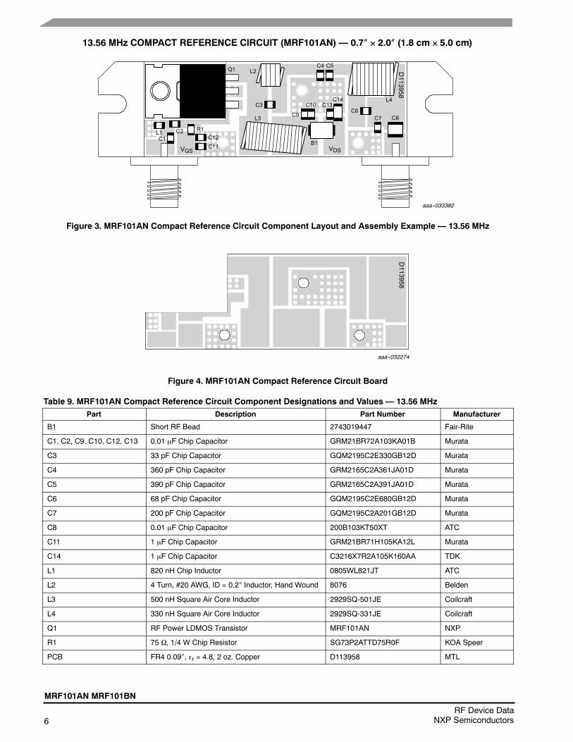
13.56 MHz COMPACT REFERENCE CIRCUIT (MRF101AN) — 0.7 2.0 (1.8 cm 5.0 cm)
Table 8. 13.56 MHz Performance (In NXP Reference Circuit, 50 ohm system)VDD = 50 Vdc, IDQ = 100 mA, Pin = 0.25 W, CW
Frequency(MHz)
Pout(W)
Gps(dB)
D(%)
13.56 130 27.1 79.6
6RF Device Data
NXP Semiconductors
MRF101AN MRF101BN
13.56 MHz COMPACT REFERENCE CIRCUIT (MRF101AN) — 0.7 2.0 (1.8 cm 5.0 cm)
Figure 3. MRF101AN Compact Reference Circuit Component Layout and Assembly Example — 13.56 MHz
C4 C5
L4
L2
C6C8C7
VDSVGSB1
L3
L1
C9
C10C14
C13
C1C2 R1
C12
C11
C3
aaa--033382
D113958
Q1
Figure 4. MRF101AN Compact Reference Circuit Board
aaa--032274
D113958
Table 9. MRF101AN Compact Reference Circuit Component Designations and Values — 13.56 MHzPart Description Part Number Manufacturer
B1 Short RF Bead 2743019447 Fair-Rite
C1, C2, C9, C10, C12, C13 0.01 F Chip Capacitor GRM21BR72A103KA01B Murata
C3 33 pF Chip Capacitor GQM2195C2E330GB12D Murata
C4 360 pF Chip Capacitor GRM2165C2A361JA01D Murata
C5 390 pF Chip Capacitor GRM2165C2A391JA01D Murata
C6 68 pF Chip Capacitor GQM2195C2E680GB12D Murata
C7 200 pF Chip Capacitor GQM2195C2A201GB12D Murata
C8 0.01 F Chip Capacitor 200B103KT50XT ATC
C11 1 F Chip Capacitor GRM21BR71H105KA12L Murata
C14 1 F Chip Capacitor C3216X7R2A105K160AA TDK
L1 820 nH Chip Inductor 0805WL821JT ATC
L2 4 Turn, #20 AWG, ID = 0.2 Inductor, Hand Wound 8076 Belden
L3 500 nH Square Air Core Inductor 2929SQ-501JE Coilcraft
L4 330 nH Square Air Core Inductor 2929SQ-331JE Coilcraft
Q1 RF Power LDMOS Transistor MRF101AN NXP
R1 75 , 1/4 W Chip Resistor SG73P2ATTD75R0F KOA Speer
PCB FR4 0.09, r = 4.8, 2 oz. Copper D113958 MTL

MRF101AN MRF101BN
7RF Device DataNXP Semiconductors
TYPICAL CHARACTERISTICS — 13.56 MHzCOMPACT REFERENCE CIRCUIT (MRF101AN)
VGS, GATE--SOURCE VOLTAGE (VOLTS)
80
60
P out,OUTPUTPOWER
(WATTS)
40
3.52.50 1.51
100
120
0
140
20
Figure 5. CW Output Power versus Gate--SourceVoltage at a Constant Input Power
Pin, INPUT POWER (WATTS)
80
60
P out,OUTPUTPOWER
(WATTS)
40
0
100
120
0
140
20
13.56 113 128
f(MHz)
P1dB(W)
P3dB(W)
Figure 6. CW Output Power versus Input Power
Pout, OUTPUT POWER (WATTS)
Figure 7. Power Gain and Drain Efficiencyversus CW Output Power
Gps,POWER
GAIN(dB)
D,DRAINEFFICIENCY(%)
27
26
30
0 20
90
70
50
30
32
24
25
28
29
31
80
60
40
20
100
40 60 80 100 120 140
0.5 2 3
VDD = 50 Vdc, f = 13.56 MHz, CW
Pin = 0.25 W
Pin = 0.12 W
0.1 0.2 0.3 0.40.25 0.35 0.45
VDD = 50 Vdc, IDQ = 100 mA, f = 13.56 MHz, CW
23
22
10
0
VDD = 50 Vdc, IDQ = 100 mA, f = 13.56 MHz, CW
D
160
0.150.05
Gps

8RF Device Data
NXP Semiconductors
MRF101AN MRF101BN
13.56 MHz COMPACT REFERENCE CIRCUIT (MRF101AN)
f(MHz)
Zsource()
Zload(
13.56 25.3 + j10.2 11.3 – j6.4
Zsource = Test circuit impedance as measured fromgate to ground.
Zload = Test circuit impedance as measured fromdrain to ground.
Figure 8. Series Equivalent Source and Load Impedance — 13.56 MHz
InputMatchingNetwork
DeviceUnderTest
OutputMatchingNetwork
Zsource Zload
5050

MRF101AN MRF101BN
9RF Device DataNXP Semiconductors
27 MHz COMPACT REFERENCE CIRCUIT (MRF101AN) — 0.7 2.0 (1.8 cm 5.0 cm)
Table 10. 27 MHz Performance (In NXP Reference Circuit, 50 ohm system)VDD = 50 Vdc, IDQ = 100 mA, Pin = 0.4 W, CW
Frequency(MHz)
Pout(W)
Gps(dB)
D(%)
27 125 24.9 79.6

10RF Device Data
NXP Semiconductors
MRF101AN MRF101BN
27 MHz COMPACT REFERENCE CIRCUIT (MRF101AN) — 0.7 2.0 (1.8 cm 5.0 cm)
Figure 9. MRF101AN Compact Reference Circuit Component Layout and Assembly Example — 27 MHz
C4 C5L4
L2
C6
C8
C9
C10C7
VDSVGS B1
L3
L1
C15
C14C13
C1
C2R1
C12C11
C3
aaa--033384
D113958
Q1
Figure 10. MRF101AN Compact Reference Circuit Board
aaa--032274
D113958
Table 11. MRF101AN Compact Reference Circuit Component Designations and Values — 27 MHzPart Description Part Number Manufacturer
B1 Short RF Bead 2743019447 Fair-Rite
C1 82 pF Chip Capacitor GQM2195C2E820GB12D Murata
C2 200 pF Chip Capacitor GQM2195C2A201GB12D Murata
C3 33 pF Chip Capacitor GQM2195C2E330GB12D Murata
C4, C5 160 pF Chip Capacitor GQM2195C2A161JB12D Murata
C6 15 pF Chip Capacitor GQM2195C2E150FB12D Murata
C7 100 pF Chip Capacitor GQM2195C2E101GB12D Murata
C8, C9, C10 1000 pF Chip Capacitor GRM2165C2A102JA01D Murata
C11 1 F Chip Capacitor 08055C105KAT2A AVX
C12, C13 0.01 F Chip Capacitor GRM21BR72A103KA01B Murata
C14 1 F Chip Capacitor CL31B105KCHSNNE Samsung
C15 6.8 nF Chip Capacitor GRM32QR73A682KW Murata
L1 270 nH Chip Inductor 0805WL221JT ATC
L2 39 nH Chip Inductor 1812SMS-39NJLC Coilcraft
L3 300 nH Square Air Core Inductor 2222SQ-301JE Coilcraft
L4 180 nH Square Air Core Inductor 2222SQ-181JE Coilcraft
Q1 RF Power LDMOS Transistor MRF101AN NXP
R1 75 , 1/4 W Chip Resistor SG73P2ATTD75R0F KOA Speer
PCB FR4 0.09, r = 4.8, 2 oz. Copper D113958 MTL
MRF101AN MRF101BN
11RF Device DataNXP Semiconductors
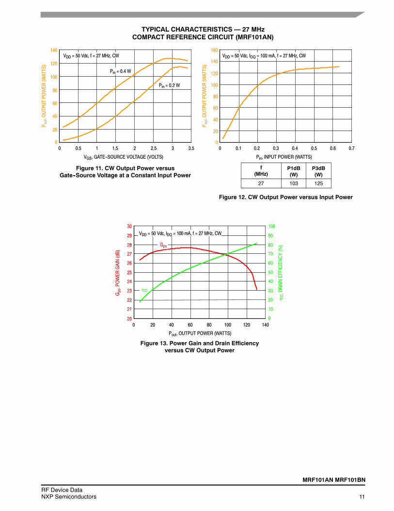
TYPICAL CHARACTERISTICS — 27 MHzCOMPACT REFERENCE CIRCUIT (MRF101AN)
VGS, GATE--SOURCE VOLTAGE (VOLTS)
80
60
P out,OUTPUTPOWER
(WATTS)
40
3.52.50 1.51
100
120
0
140
20
Figure 11. CW Output Power versusGate--Source Voltage at a Constant Input Power
Pin, INPUT POWER (WATTS)
80
60
P out,OUTPUTPOWER
(WATTS)
40
0
100
120
0
160
20
27 103 125
f(MHz)
P1dB(W)
P3dB(W)
Figure 12. CW Output Power versus Input Power
Pout, OUTPUT POWER (WATTS)
Figure 13. Power Gain and Drain Efficiencyversus CW Output Power
Gps,POWER
GAIN(dB)
D,DRAINEFFICIENCY(%)
25
24
28
0 20
90
70
50
30
30
22
23
26
27
29
80
60
40
20
100
40 60 80 100 120 140
0.5 2 3
VDD = 50 Vdc, f = 27 MHz, CW
Pin = 0.4 W
Pin = 0.2 W
0.1 0.2 0.3 0.4 0.5 0.6 0.7
VDD = 50 Vdc, IDQ = 100 mA, f = 27 MHz, CW
21
20
10
0
VDD = 50 Vdc, IDQ = 100 mA, f = 27 MHz, CW
Gps
D
140

12RF Device Data
NXP Semiconductors
MRF101AN MRF101BN
27 MHz COMPACT REFERENCE CIRCUIT (MRF101AN)
f(MHz)
Zsource()
Zload()
27 28.9 + j14.7 12.9 – j5.3
Zsource = Test circuit impedance as measured fromgate to ground.
Zload = Test circuit impedance as measured fromdrain to ground.
Figure 14. Series Equivalent Source and Load Impedance — 27 MHz
InputMatchingNetwork
DeviceUnderTest
OutputMatchingNetwork
Zsource Zload
5050
MRF101AN MRF101BN
13RF Device DataNXP Semiconductors
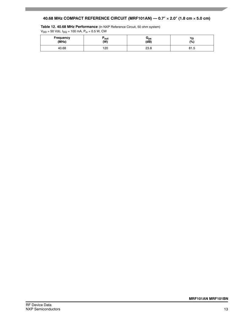
40.68 MHz COMPACT REFERENCE CIRCUIT (MRF101AN) — 0.7 2.0 (1.8 cm 5.0 cm)
Table 12. 40.68 MHz Performance (In NXP Reference Circuit, 50 ohm system)VDD = 50 Vdc, IDQ = 100 mA, Pin = 0.5 W, CW
Frequency(MHz)
Pout(W)
Gps(dB)
D(%)
40.68 120 23.8 81.5
14RF Device Data
NXP Semiconductors
MRF101AN MRF101BN
40.68 MHz COMPACT REFERENCE CIRCUIT (MRF101AN) — 0.7 2.0 (1.8 cm 5.0 cm)
Figure 15. MRF101AN Compact Reference Circuit Component Layout and Assembly Example — 40.68 MHz
C4L4L2
C5C6 C8
C7
VDSVGS
B1L3
L1
C9
C10
C14
C13
C1C2 R1
C12
C11
C3
aaa--032273
D113958
Q1
Figure 16. MRF101AN Compact Reference Circuit Board
aaa--032274
D113958
Table 13. MRF101AN Compact Reference Circuit Component Designations and Values — 40.68 MHzPart Description Part Number Manufacturer
B1 Short RF Bead 2743019447 Fair-Rite
C1, C5 82 pF Chip Capacitor GQM2195C2E820GB12D Murata
C2, C4 200 pF Chip Capacitor GQM2195C2A201GB12D Murata
C3 33 pF Chip Capacitor GQM2195C2E330GB12D Murata
C6, C7, C8, C9, C10 1000 pF Chip Capacitor GRM2165C2A102JA01D Murata
C11 1 F Chip Capacitor GJ821BR71H105KA12L Murata
C12, C13 0.01 F Chip Capacitor GRM21BR72A103KA01B Murata
C14 1 F Chip Capacitor C3216X7R2A105K160AA TDK
L1 150 nH Chip Inductor 0805WL151JT ATC
L2 17.5 nH, 4 Turn Inductor GA3095-ACL Coilcraft
L3 160 nH Square Air Core Inductor 2222SQ-161JEC Coilcraft
L4 110 nH Square Air Core Inductor 2222SQ-111JEB Coilcraft
Q1 RF Power LDMOS Transistor MRF101AN NXP
R1 75 , 1/4 W Chip Resistor SG73P2ATTD75R0F KOA Speer
PCB FR4 0.09, r = 4.8, 2 oz. Copper D113958 MTL
MRF101AN MRF101BN
15RF Device DataNXP Semiconductors
TYPICAL CHARACTERISTICS — 40.68 MHzCOMPACT REFERENCE CIRCUIT (MRF101AN)
VGS, GATE--SOURCE VOLTAGE (VOLTS)
80
60
P out,OUTPUTPOWER
(WATTS)
40
3.52.50 1.51
100
120
0
140
20
Figure 17. CW Output Power versusGate--Source Voltage at a Constant Input Power
Pin, INPUT POWER (WATTS)
80
60
P out,OUTPUTPOWER
(WATTS)
40
0
100
120
0
140
20
40.68 101 121
f(MHz)
P1dB(W)
P3dB(W)
Figure 18. CW Output Power versus Input Power
Pout, OUTPUT POWER (WATTS)
Figure 19. Power Gain and Drain Efficiencyversus CW Output Power
Gps,POWER
GAIN(dB)
D,DRAINEFFICIENCY(%)
25
24
28
0 20
90
70
50
30
30
22
23
26
27
29
80
60
40
20
100
40 60 80 100 120 140
0.5 2 3
VDD = 50 Vdc, f = 40.68 MHz, CW
Pin = 0.5 W
Pin = 0.25 W
0.1 0.2 0.3 0.4 0.5 0.6 0.7
VDD = 50 Vdc, IDQ = 100 mA, f = 40.68 MHz, CW
21
20
10
0
VDD = 50 Vdc, IDQ = 100 mA, f = 40.68 MHz, CW
Gps
D
16RF Device Data
NXP Semiconductors
MRF101AN MRF101BN
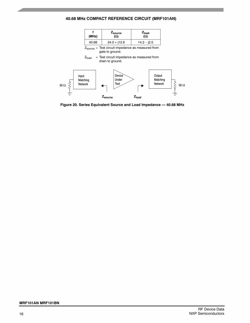
40.68 MHz COMPACT REFERENCE CIRCUIT (MRF101AN)
f(MHz)
Zsource()
Zload()
40.68 24.0 + j12.6 14.2 – j2.5
Zsource = Test circuit impedance as measured fromgate to ground.
Zload = Test circuit impedance as measured fromdrain to ground.
Figure 20. Series Equivalent Source and Load Impedance — 40.68 MHz
InputMatchingNetwork
DeviceUnderTest
OutputMatchingNetwork
Zsource Zload
5050

MRF101AN MRF101BN
17RF Device DataNXP Semiconductors
50 MHz COMPACT REFERENCE CIRCUIT (MRF101AN) — 0.7 2.0 (1.8 cm 5.0 cm)
Table 14. 50 MHz Performance (In NXP Reference Circuit, 50 ohm system)VDD = 50 Vdc, IDQ = 100 mA, Pin = 0.64 W, CW
Frequency(MHz)
Pout(W)
Gps(dB)
D(%)
50 119 22.8 82.1

18RF Device Data
NXP Semiconductors
MRF101AN MRF101BN
50 MHz COMPACT REFERENCE CIRCUIT (MRF101AN) — 0.7 2.0 (1.8 cm 5.0 cm)
Figure 21. MRF101AN Compact Reference Circuit Component Layout and Assembly Example — 50 MHz
L4
L2
C5C6 C8
C7
VDSVGS B1
L3L1
C4
C3
C13C10
C9
C1C2
R1C12
C11
aaa--033386
D113958
Q1
Figure 22. MRF101AN Compact Reference Circuit Board
aaa--032274
D113958
Table 15. MRF101AN Compact Reference Circuit Component Designations and Values — 50 MHzPart Description Part Number Manufacturer
B1 Short RF Bead 2743019447 Fair-Rite
C1 82 pF Chip Capacitor GQM2195C2E820GB12D Murata
C2 200 pF Chip Capacitor GQM2195C2A201GB12D Murata
C3 1 F Chip Capacitor CL31B105KCHSNNE Samsung
C4 180 pF Chip Capacitor GQM2195C2A181GB12D Murata
C5 68 pF Chip Capacitor GQM2195C2E680GB12D Murata
C6, C7, C8, C9, C10 1000 pF Chip Capacitor GRM2165C2A102JA01D Murata
C11 1 F Chip Capacitor 08055C105KAT2A AVX
C12, C13 0.01 F Chip Capacitor GRM21BR72A103KA01B Murata
L1 100 nH Chip Inductor 0805WL101JT ATC
L2 17.5 nH Air Core Inductor GA3095-ALC Coilcraft
L3 160 nH Square Air Core Inductor 2222SQ-161JEC Coilcraft
L4 110 nH Square Air Core Inductor 2222SQ-111JEB Coilcraft
Q1 RF Power LDMOS Transistor MRF101AN NXP
R1 75 , 1/4 W Chip Resistor SG73P2ATTD75R0F KOA Speer
PCB FR4 0.09, r = 4.8, 2 oz. Copper D113958 MTL
MRF101AN MRF101BN
19RF Device DataNXP Semiconductors
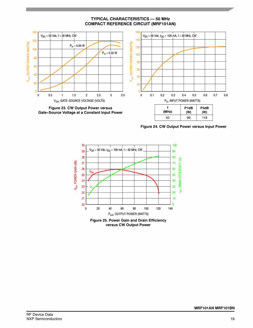
TYPICAL CHARACTERISTICS — 50 MHzCOMPACT REFERENCE CIRCUIT (MRF101AN)
VGS, GATE--SOURCE VOLTAGE (VOLTS)
80
60
P out,OUTPUTPOWER
(WATTS)
40
3.52.50 1.51
100
120
0
140
20
Figure 23. CW Output Power versusGate--Source Voltage at a Constant Input Power
Pin, INPUT POWER (WATTS)
80
60
P out,OUTPUTPOWER
(WATTS)
40
0
100
120
0
160
20
50 99 118
f(MHz)
P1dB(W)
P3dB(W)
Figure 24. CW Output Power versus Input Power
Pout, OUTPUT POWER (WATTS)
Figure 25. Power Gain and Drain Efficiencyversus CW Output Power
Gps,POWER
GAIN(dB)
D,DRAINEFFICIENCY(%)
25
24
28
0 20
90
70
50
30
30
22
23
26
27
29
80
60
40
20
100
40 60 80 100 120 140
0.5 2 3
VDD = 50 Vdc, f = 50 MHz, CW
Pin = 0.64 W
Pin = 0.32 W
0.1 0.2 0.3 0.4 0.5 0.6 0.8
VDD = 50 Vdc, IDQ = 100 mA, f = 50 MHz, CW
21
20
10
0
VDD = 50 Vdc, IDQ = 100 mA, f = 50 MHz, CW
Gps
D
140
0.7
20RF Device Data
NXP Semiconductors
MRF101AN MRF101BN
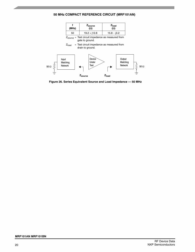
50 MHz COMPACT REFERENCE CIRCUIT (MRF101AN)
f(MHz)
Zsource()
Zload()
50 19.2 + j12.8 15.8 – j3.2
Zsource = Test circuit impedance as measured fromgate to ground.
Zload = Test circuit impedance as measured fromdrain to ground.
Figure 26. Series Equivalent Source and Load Impedance — 50 MHz
InputMatchingNetwork
DeviceUnderTest
OutputMatchingNetwork
Zsource Zload
5050

MRF101AN MRF101BN
21RF Device DataNXP Semiconductors
81.36 MHz REFERENCE CIRCUIT (MRF101AN) — 2.0 3.0 (5.0 cm 7.6 cm)
Table 16. 81.36 MHz Performance (In NXP Reference Circuit, 50 ohm system)VDD = 50 Vdc, IDQ = 100 mA, Pin = 0.64 W, CW
Frequency(MHz)
Pout(W)
Gps(dB)
D(%)
81.36 130 23.2 80.8
22RF Device Data
NXP Semiconductors
MRF101AN MRF101BN
81.36 MHz REFERENCE CIRCUIT (MRF101AN) — 2.0 3.0 (5.0 cm 7.6 cm)
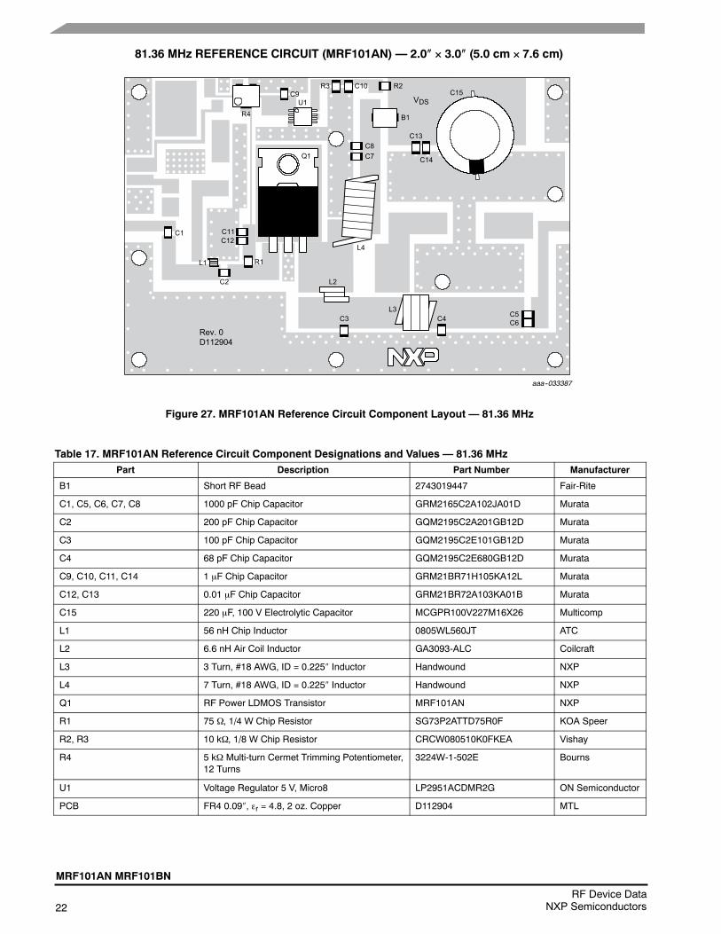
Figure 27. MRF101AN Reference Circuit Component Layout — 81.36 MHz
Q1
C8
B1
R2C9
C1
R1L1
L2
L4
C3 C4C5C6
L3
C11C12
C2
Rev. 0D112904
C13
C14
C15VDS
C10R3
R4
U1
C7
aaa--033387
Table 17. MRF101AN Reference Circuit Component Designations and Values — 81.36 MHzPart Description Part Number Manufacturer
B1 Short RF Bead 2743019447 Fair-Rite
C1, C5, C6, C7, C8 1000 pF Chip Capacitor GRM2165C2A102JA01D Murata
C2 200 pF Chip Capacitor GQM2195C2A201GB12D Murata
C3 100 pF Chip Capacitor GQM2195C2E101GB12D Murata
C4 68 pF Chip Capacitor GQM2195C2E680GB12D Murata
C9, C10, C11, C14 1 F Chip Capacitor GRM21BR71H105KA12L Murata
C12, C13 0.01 F Chip Capacitor GRM21BR72A103KA01B Murata
C15 220 F, 100 V Electrolytic Capacitor MCGPR100V227M16X26 Multicomp
L1 56 nH Chip Inductor 0805WL560JT ATC
L2 6.6 nH Air Coil Inductor GA3093-ALC Coilcraft
L3 3 Turn, #18 AWG, ID = 0.225 Inductor Handwound NXP
L4 7 Turn, #18 AWG, ID = 0.225 Inductor Handwound NXP
Q1 RF Power LDMOS Transistor MRF101AN NXP
R1 75 , 1/4 W Chip Resistor SG73P2ATTD75R0F KOA Speer
R2, R3 10 k, 1/8 W Chip Resistor CRCW080510K0FKEA Vishay
R4 5 k Multi-turn Cermet Trimming Potentiometer,12 Turns
3224W-1-502E Bourns
U1 Voltage Regulator 5 V, Micro8 LP2951ACDMR2G ON Semiconductor
PCB FR4 0.09, r = 4.8, 2 oz. Copper D112904 MTL
MRF101AN MRF101BN
23RF Device DataNXP Semiconductors
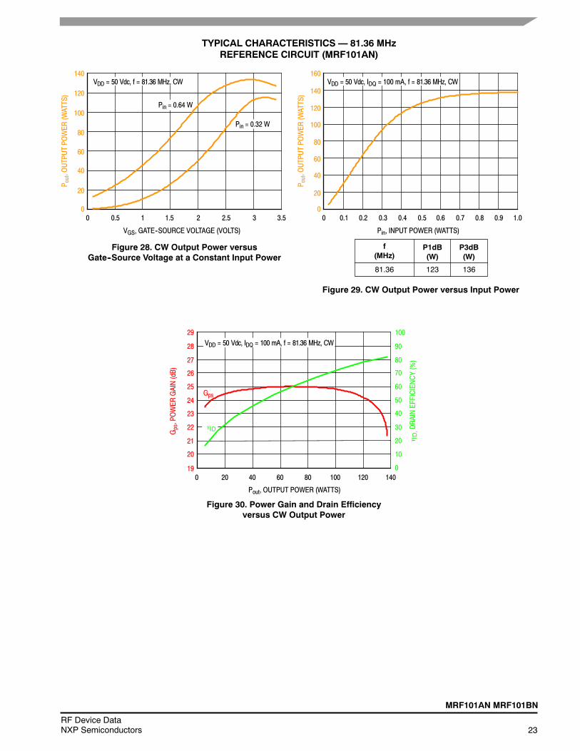
TYPICAL CHARACTERISTICS — 81.36 MHzREFERENCE CIRCUIT (MRF101AN)
VGS, GATE--SOURCE VOLTAGE (VOLTS)
80
60
P out,OUTPUTPOWER
(WATTS)
40
3.52.50 1.51
100
120
0
140
20
Figure 28. CW Output Power versusGate--Source Voltage at a Constant Input Power
Pin, INPUT POWER (WATTS)
80
60
P out,OUTPUTPOWER
(WATTS)
40
0
100
120
0
160
20
81.36 123 136
f(MHz)
P1dB(W)
P3dB(W)
Figure 29. CW Output Power versus Input Power
Pout, OUTPUT POWER (WATTS)
Figure 30. Power Gain and Drain Efficiencyversus CW Output Power
Gps,POWER
GAIN(dB)
D,DRAINEFFICIENCY(%)
24
23
27
0 20
90
70
50
30
29
21
22
25
26
28
80
60
40
20
100
40 60 80 100 120 140
0.5 2 3
VDD = 50 Vdc, f = 81.36 MHz, CW
Pin = 0.64 W
Pin = 0.32 W
0.1 0.2 0.3 0.4 0.5 0.6 1.0
VDD = 50 Vdc, IDQ = 100 mA, f = 81.36 MHz, CW
20
19
10
0
VDD = 50 Vdc, IDQ = 100 mA, f = 81.36 MHz, CW
Gps
D
140
0.7 0.8 0.9
24RF Device Data
NXP Semiconductors
MRF101AN MRF101BN
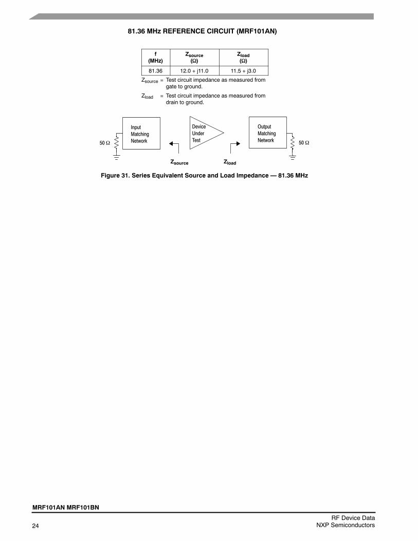
81.36 MHz REFERENCE CIRCUIT (MRF101AN)
f(MHz)
Zsource()
Zload()
81.36 12.0 + j11.0 11.5 + j3.0
Zsource = Test circuit impedance as measured fromgate to ground.
Zload = Test circuit impedance as measured fromdrain to ground.
Figure 31. Series Equivalent Source and Load Impedance — 81.36 MHz
InputMatchingNetwork
DeviceUnderTest
OutputMatchingNetwork
Zsource Zload
5050

MRF101AN MRF101BN
25RF Device DataNXP Semiconductors
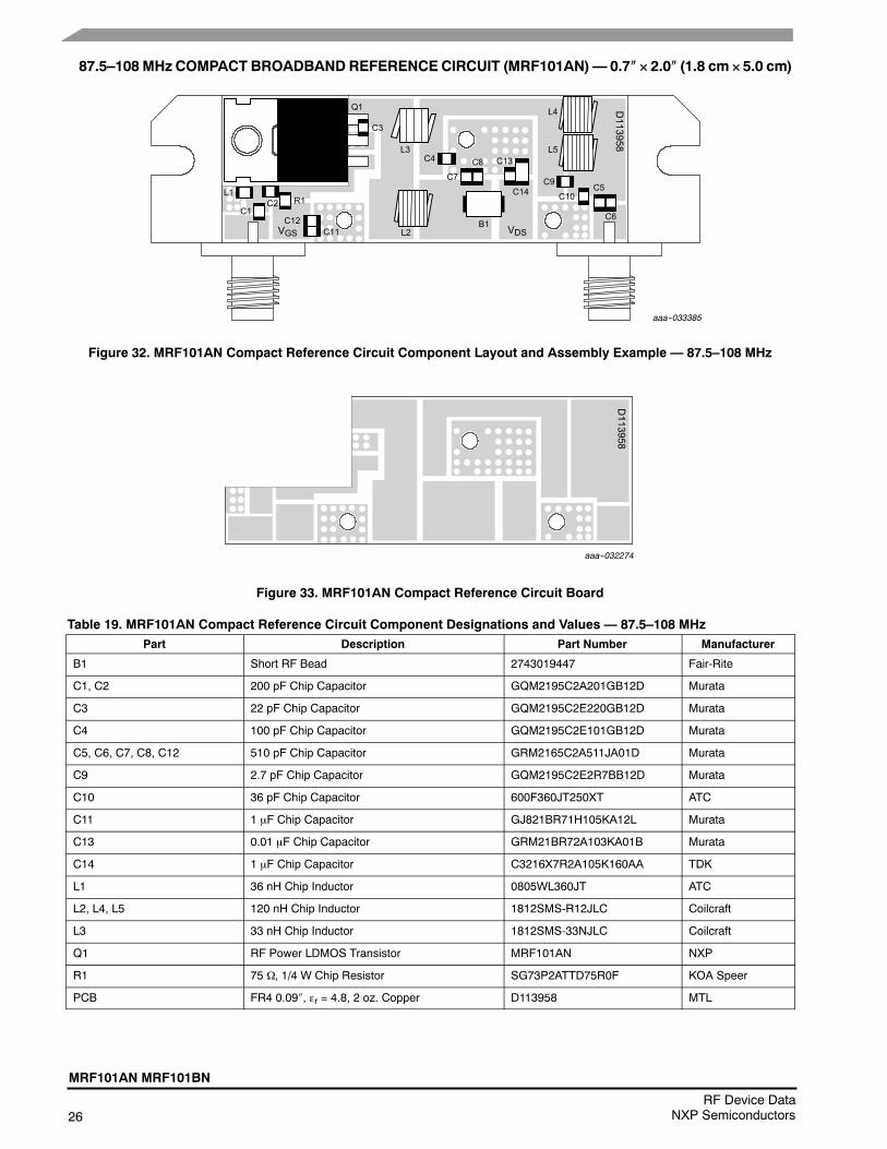
87.5–108 MHz COMPACT BROADBAND REFERENCE CIRCUIT (MRF101AN) — 0.7 2.0 (1.8 cm 5.0 cm)
Table 18. 87.5–108 MHz Broadband Performance (In NXP Reference Circuit, 50 ohm system)VDD = 50 Vdc, IDQ = 100 mA, Pin = 1 W, CW
Frequency(MHz)
Pout(W)
Gps(dB)
D(%)
87.5 122 20.8 79.0
98 115 20.6 76.8
108 115 20.6 76.0
26RF Device Data
NXP Semiconductors
MRF101AN MRF101BN
87.5–108 MHz COMPACT BROADBANDREFERENCE CIRCUIT (MRF101AN)— 0.7 2.0 (1.8 cm 5.0 cm)
Figure 32. MRF101AN Compact Reference Circuit Component Layout and Assembly Example — 87.5–108 MHz
L4
L5L3
C5
C6
C9
C10
VDSVGSB1
L2
L1
C4
C14
C13C8
C7
C1C2 R1
C11C12
C3
aaa--033385
D113958
Q1
Figure 33. MRF101AN Compact Reference Circuit Board
aaa--032274
D113958
Table 19. MRF101AN Compact Reference Circuit Component Designations and Values — 87.5–108 MHzPart Description Part Number Manufacturer
B1 Short RF Bead 2743019447 Fair-Rite
C1, C2 200 pF Chip Capacitor GQM2195C2A201GB12D Murata
C3 22 pF Chip Capacitor GQM2195C2E220GB12D Murata
C4 100 pF Chip Capacitor GQM2195C2E101GB12D Murata
C5, C6, C7, C8, C12 510 pF Chip Capacitor GRM2165C2A511JA01D Murata
C9 2.7 pF Chip Capacitor GQM2195C2E2R7BB12D Murata
C10 36 pF Chip Capacitor 600F360JT250XT ATC
C11 1 F Chip Capacitor GJ821BR71H105KA12L Murata
C13 0.01 F Chip Capacitor GRM21BR72A103KA01B Murata
C14 1 F Chip Capacitor C3216X7R2A105K160AA TDK
L1 36 nH Chip Inductor 0805WL360JT ATC
L2, L4, L5 120 nH Chip Inductor 1812SMS-R12JLC Coilcraft
L3 33 nH Chip Inductor 1812SMS-33NJLC Coilcraft
Q1 RF Power LDMOS Transistor MRF101AN NXP
R1 75 , 1/4 W Chip Resistor SG73P2ATTD75R0F KOA Speer
PCB FR4 0.09, r = 4.8, 2 oz. Copper D113958 MTL
MRF101AN MRF101BN
27RF Device DataNXP Semiconductors
TYPICAL CHARACTERISTICS — 87.5–108 MHzCOMPACT BROADBAND REFERENCE CIRCUIT (MRF101AN)
19
f = 87.5 MHz
108 MHz
93
f, FREQUENCY (MHz)
25
24
90
85
80
75
65
130
120
D,DRAIN
EFFICIENCY(%)
D
Gps,POWER
GAIN(dB)
23
22
21
20
1695 97 99 101
70
110
P out,OUTPUT
POWER
(WATTS)
VDD = 50 Vdc, Pin = 1 W, lDQ = 100 mA, CW
9189 10987
18
10017
Gps
0
Pin, INPUT POWER (WATTS)
0
P out,OUTPUTPOWER
(WATTS)
80
60
40
20
0.4 0.6
120
100
0.2
VDD = 50 Vdc, IDQ = 100 mA, CW
0.8
140
1.4
27
20
24
22
80
75
70
Gps,POWER
GAIN(dB)
20
40 60
26
85
Gps
D
80
25
23
21
100 120 140
VDD = 50 Vdc, lDQ = 100 mA, CW f = 87.5 MHz
108 MHz
65
60
55
50
98 MHz
87.5 MHz
108 MHz98 MHz
D,DRAINEFFICIENCY(%)
Figure 34. Power Gain, Drain Efficiency and CW OutputPower versus Frequency at a Constant Input Power
Figure 35. CW Output Power versus Input Power and Frequency
Pout, OUTPUT POWER (WATTS)
Figure 36. Power Gain and Drain Efficiency versusCW Output Power and Frequency
98 MHz
19
18
17
45
40
35
107105103
Pout
1.0 1.2
28RF Device Data
NXP Semiconductors
MRF101AN MRF101BN
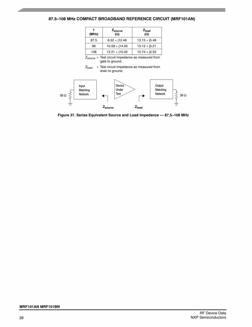
87.5–108 MHz COMPACT BROADBAND REFERENCE CIRCUIT (MRF101AN)
f(MHz)
Zsource()
Zload()
87.5 8.52 + j12.46 13.15 + j5.48
98 10.59 + j14.03 13.12 + j5.21
108 12.21 + j15.02 10.74 + j5.52
Zsource = Test circuit impedance as measured fromgate to ground.
Zload = Test circuit impedance as measured fromdrain to ground.
Figure 37. Series Equivalent Source and Load Impedance — 87.5–108 MHz
InputMatchingNetwork
DeviceUnderTest
OutputMatchingNetwork
Zsource Zload
5050
MRF101AN MRF101BN
29RF Device DataNXP Semiconductors
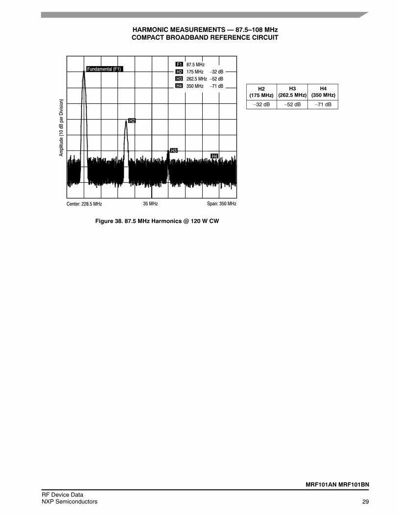
HARMONIC MEASUREMENTS — 87.5–108 MHzCOMPACT BROADBAND REFERENCE CIRCUIT
H2(175 MHz)
H3(262.5 MHz)
H4(350 MHz)
–32 dB –52 dB –71 dB
Center: 228.5 MHz Span: 350 MHz35 MHz
Figure 38. 87.5 MHz Harmonics @ 120 W CW
H4H3
H2
175 MHz –32 dB262.5 MHz –52 dB350 MHz –71 dB
H2H3H4
F1 87.5 MHzFundamental (F1)
Amplitude(10dB
perDivision)
30RF Device Data
NXP Semiconductors
MRF101AN MRF101BN
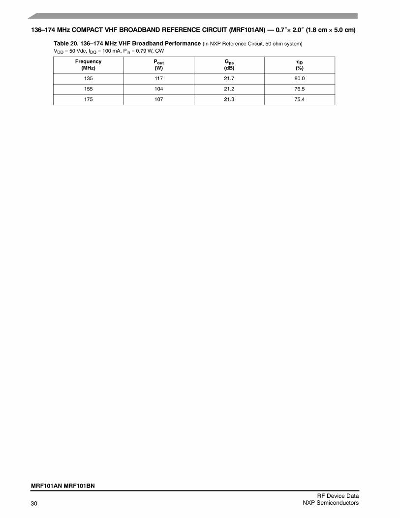
136–174 MHz COMPACT VHF BROADBAND REFERENCE CIRCUIT (MRF101AN) — 0.7 2.0 (1.8 cm 5.0 cm)
Table 20. 136–174 MHz VHF Broadband Performance (In NXP Reference Circuit, 50 ohm system)VDD = 50 Vdc, IDQ = 100 mA, Pin = 0.79 W, CW
Frequency(MHz)
Pout(W)
Gps(dB)
D(%)
135 117 21.7 80.0
155 104 21.2 76.5
175 107 21.3 75.4
MRF101AN MRF101BN
31RF Device DataNXP Semiconductors
136–174 MHz COMPACT VHF BROADBAND REFERENCE CIRCUIT (MRF101AN) — 0.7 2.0 (1.8 cm 5.0 cm)
Figure 39. MRF101AN Compact Reference Circuit Component Layout and Assembly Example — 136–174 MHz
aaa--032286
C9
L5
L1
L2C2
C1
L4
C7
C8
C3
C13
C14
B1
L3
L6
C12
C6
C5C4
R1
C11 VDSVGSD113958
Q1
Note: Component number C10 is not used.
Figure 40. MRF101AN Compact Reference Circuit Board
aaa--032285
D113958
Table 21. MRF101AN Compact VHF Broadband Reference Circuit Component Designations and Values — 136–174 MHzPart Description Part Number Manufacturer
B1 Short RF Bead 2743019447 Fair-Rite
C1 39 pF Chip Capacitor GQM2195C2E390GB12D Murata
C2, C5, C6, C7, C8, C12 510 pF Chip Capacitor GRM2165C2A511JA01D Murata
C3 68 pF Chip Capacitor GQM2195C2E680GB12D Murata
C4 27 pF Chip Capacitor GQM2195C2E270GB12D Murata
C9 10 pF Chip Capacitor GQM2195C2E100FB12D Murata
C11 1 F Chip Capacitor GJ821BR71H105KA12L Murata
C13 0.01 F Chip Capacitor GRM21BR72A103KA01B Murata
C14 1 F Chip Capacitor C3216X7R2A105K160AA TDK
L1 22 nH Chip Inductor 0805WL220JT ATC
L2 12 nH Chip Inductor 0805WL120JT ATC
L3, L4, L6 68 nH Air Core Inductor 1812SMS-68NJLC Coilcraft
L5 12 nH, 3 Turn Inductor GA3094-ALC Coilcraft
Q1 RF Power LDMOS Transistor MRF101AN NXP
R1 75 , 1/4 W Chip Resistor SG73P2ATTD75R0F KOA Speer
PCB FR4 0.09 r = 4.8, 2 oz. Copper D113958 MTL

32RF Device Data
NXP Semiconductors
MRF101AN MRF101BN
TYPICAL CHARACTERISTICS — 136–174 MHzCOMPACT VHF BROADBAND REFERENCE CIRCUIT (MRF101AN)
f = 135 MHz
155 MHz
0
Pin, INPUT POWER (WATTS)
0
P out,OUTPUTPOWER
(WATTS)
80
60
40
20
0.4 0.6
120
100
0.2
VDD = 50 Vdc, IDQ = 100 mA, CW
0.8
140
1.0
175 MHz
20
150
f, FREQUENCY (MHz)
26
25
90
85
80
75
65
130
120
D,DRAIN
EFFICIENCY(%)
D
Gps,POWER
GAIN(dB)
24
23
22
21
17155 160 165 170
70
110
P out,OUTPUT
POWER
(WATTS)
VDD = 50 Vdc, Pin = 0.79 W, lDQ = 100 mA, CW
Pout
145140 175135
19
10018
Gps
Figure 41. Power Gain, Drain Efficiency and CW OutputPower versus Frequency at a Constant Input Power
VGS, GATE--SOURCE VOLTAGE (VOLTS)
80
60
P out,OUTPUTPOWER
(WATTS)
40
3.52.50 1.51
100
120
0
140
20
Figure 42. CW Output Power versusGate--Source Voltage at a Constant Input Power
0.5 2 3
VDD = 50 Vdc, f = 155 MHz, CW
Pin = 0.79 W
Pin = 0.4 W
Figure 43. CW Output Power versusInput Power and Frequency
27
20
24
22
80
75
70
Gps,POWER
GAIN(dB)
20
40 60
26
85
Gps
D
80
25
23
21
100 120 140
VDD = 50 Vdc, lDQ = 100 mA, CW f = 155 MHz
175 MHz65
60
55
50
135 MHz
135 MHz155 MHz
175 MHz D,DRAINEFFICIENCY(%)
Pout, OUTPUT POWER (WATTS)
Figure 44. Power Gain and Drain Efficiency versusCW Output Power and Frequency
19
18
17
45
40
35
MRF101AN MRF101BN
33RF Device DataNXP Semiconductors
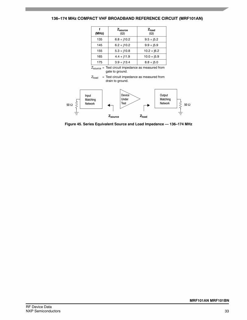
136–174 MHz COMPACT VHF BROADBAND REFERENCE CIRCUIT (MRF101AN)
f(MHz)
Zsource
Zload
135 6.8 + j10.2 9.5 + j5.2
145 6.2 + j10.2 9.9 + j5.9
155 5.3 + j10.8 10.2 + j6.2
165 4.4 + j11.9 10.0 + j5.9
175 3.9 + j13.4 8.8 + j5.0
Zsource = Test circuit impedance as measured fromgate to ground.
Zload = Test circuit impedance as measured fromdrain to ground.
Figure 45. Series Equivalent Source and Load Impedance — 136–174 MHz
InputMatchingNetwork
DeviceUnderTest
OutputMatchingNetwork
Zsource Zload
5050
34RF Device Data
NXP Semiconductors
MRF101AN MRF101BN
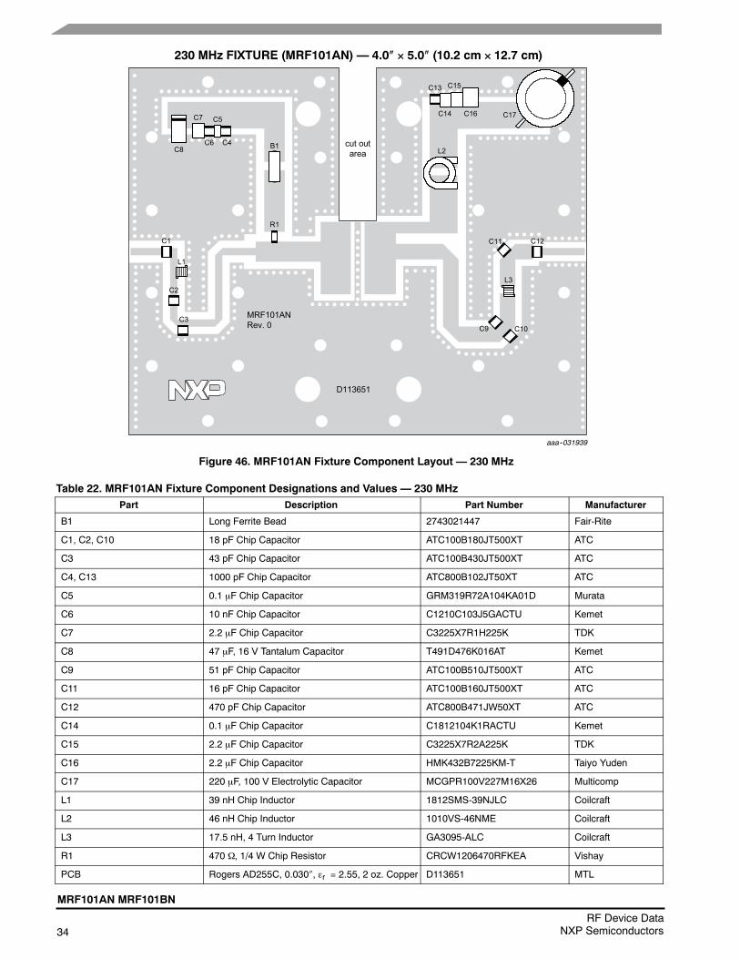
230 MHz FIXTURE (MRF101AN) — 4.0 5.0 (10.2 cm 12.7 cm)
Figure 46. MRF101AN Fixture Component Layout — 230 MHz
cut outarea
MRF101ANRev. 0
D113651
C8 B1
R1
C2
C3
L1
L3
C1
C7
C6
C5C14 C16
L2
C11 C12
C9 C10
C15
C17
C13
C4
aaa--031939
Table 22. MRF101AN Fixture Component Designations and Values — 230 MHzPart Description Part Number Manufacturer
B1 Long Ferrite Bead 2743021447 Fair-Rite
C1, C2, C10 18 pF Chip Capacitor ATC100B180JT500XT ATC
C3 43 pF Chip Capacitor ATC100B430JT500XT ATC
C4, C13 1000 pF Chip Capacitor ATC800B102JT50XT ATC
C5 0.1 F Chip Capacitor GRM319R72A104KA01D Murata
C6 10 nF Chip Capacitor C1210C103J5GACTU Kemet
C7 2.2 F Chip Capacitor C3225X7R1H225K TDK
C8 47 F, 16 V Tantalum Capacitor T491D476K016AT Kemet
C9 51 pF Chip Capacitor ATC100B510JT500XT ATC
C11 16 pF Chip Capacitor ATC100B160JT500XT ATC
C12 470 pF Chip Capacitor ATC800B471JW50XT ATC
C14 0.1 F Chip Capacitor C1812104K1RACTU Kemet
C15 2.2 F Chip Capacitor C3225X7R2A225K TDK
C16 2.2 F Chip Capacitor HMK432B7225KM-T Taiyo Yuden
C17 220 F, 100 V Electrolytic Capacitor MCGPR100V227M16X26 Multicomp
L1 39 nH Chip Inductor 1812SMS-39NJLC Coilcraft
L2 46 nH Chip Inductor 1010VS-46NME Coilcraft
L3 17.5 nH, 4 Turn Inductor GA3095-ALC Coilcraft
R1 470 , 1/4 W Chip Resistor CRCW1206470RFKEA Vishay
PCB Rogers AD255C, 0.030, r = 2.55, 2 oz. Copper D113651 MTL
MRF101AN MRF101BN
35RF Device DataNXP Semiconductors
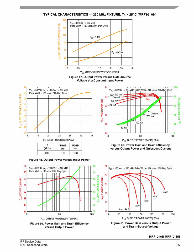
TYPICAL CHARACTERISTICS — 230 MHz FIXTURE, TC = 25_C (MRF101AN)
0
VGS, GATE--SOURCE VOLTAGE (VOLTS)
Figure 47. Output Power versus Gate--SourceVoltage at a Constant Input Power
0
P out,OUTPUTPOWER
(WATTS)PEAK
75
50
25
1.5 2 2.5 3
125
100Pin = 0.9 W
Pin = 0.45 W
0.5 1
VDD = 50 Vdc, f = 230 MHzPulse Width = 100 sec, 20% Duty Cycle
Pin, INPUT POWER (dBm) PEAK
51
49
43
P out,OUTPUTPOWER
(dBm
)PEAK
47
333021 2724
53
18
VDD = 50 Vdc, IDQ = 100 mA, f = 230 MHzPulse Width = 100 sec, 20% Duty Cycle
230 110 128
f(MHz)
P1dB(W)
P3dB(W)
Figure 48. Output Power versus Input Power
Pout, OUTPUT POWER (WATTS) PEAK
Figure 49. Power Gain and Drain Efficiencyversus Output Power and Quiescent Current
Gps,POWER
GAIN(dB)
D,DRAINEFFICIENCY(%)
20
18
IDQ = 300 mA22 200 mA
50 mA
3 300
80
60
40
20
100 mA
300 mA
24
D
Gps
VDD = 50 Vdc, f = 230 MHz, Pulse Width = 100 sec, 20% Duty Cycle
16
D
VDD = 50 Vdc, IDQ = 100 mA, f = 230 MHzPulse Width = 100 sec, 20% Duty Cycle
19
18
23
3 3010
80
70
60
50
40
30
20
24
Pout, OUTPUT POWER (WATTS) PEAK
Figure 50. Power Gain and Drain Efficiencyversus Output Power
Gps,POWER
GAIN(dB)
D,DRAINEFFICIENCY(%)
170
Pout, OUTPUT POWER (WATTS) PEAK
Figure 51. Power Gain versus Output Powerand Drain--Source Voltage
20
Gps,POWER
GAIN(dB)
16
1450 75 100
18
VDD = 30 V
25
50 V
22
150
45
14
100
20
21
22
45 V
125 150
Gps
300
300
24IDQ = 100 mA, f = 230 MHz, Pulse Width = 100 sec, 20% Duty Cycle
35 V
41
39
37
40 V
15
200 mA
100 mA
50 mA

36RF Device Data
NXP Semiconductors
MRF101AN MRF101BN
230 MHz FIXTURE (MRF101AN)
f(MHz)
Zsource
Zload
230 2.1 + j5.9 5.5 + j3.2
Zsource = Test circuit impedance as measured fromgate to ground.
Zload = Test circuit impedance as measured fromdrain to ground.
Figure 52. Series Equivalent Source and Load Impedance — 230 MHz
InputMatchingNetwork
DeviceUnderTest
OutputMatchingNetwork
Zsource Zload
5050
MRF101AN MRF101BN
37RF Device DataNXP Semiconductors
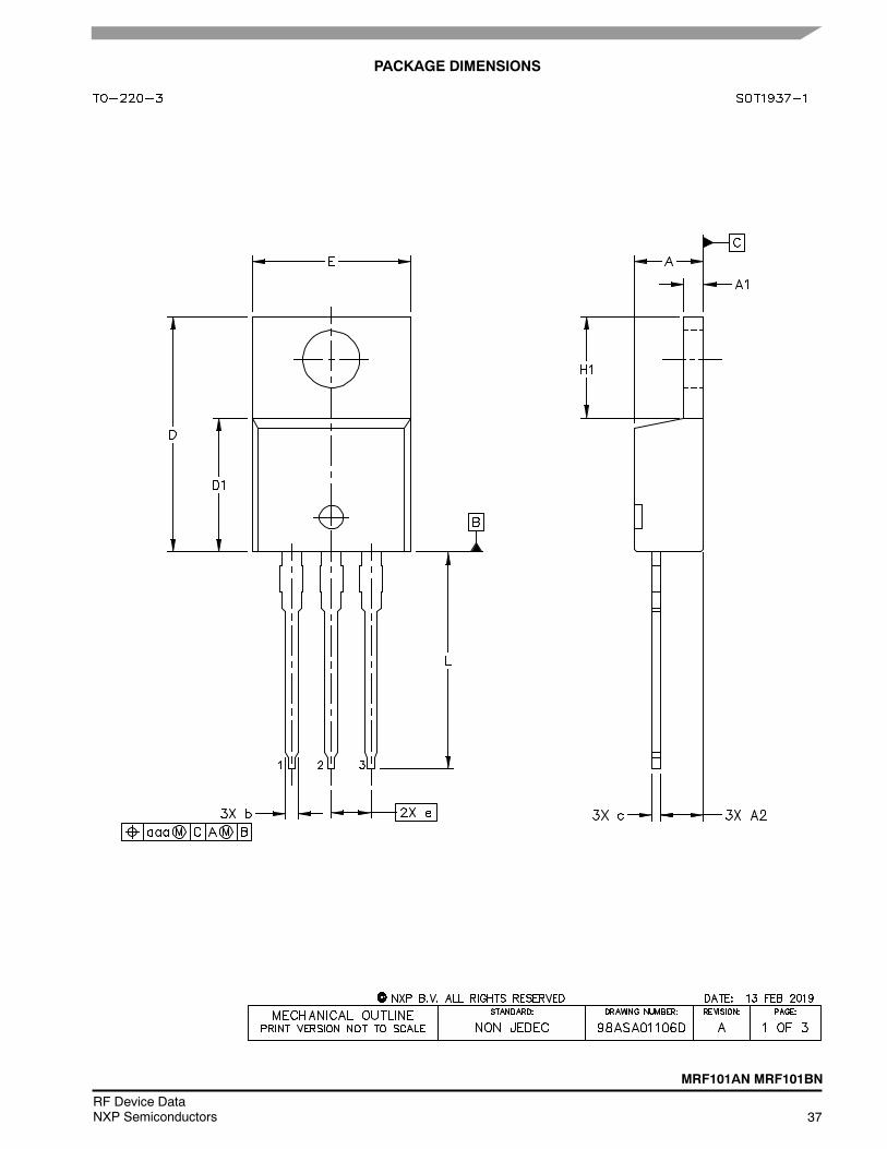
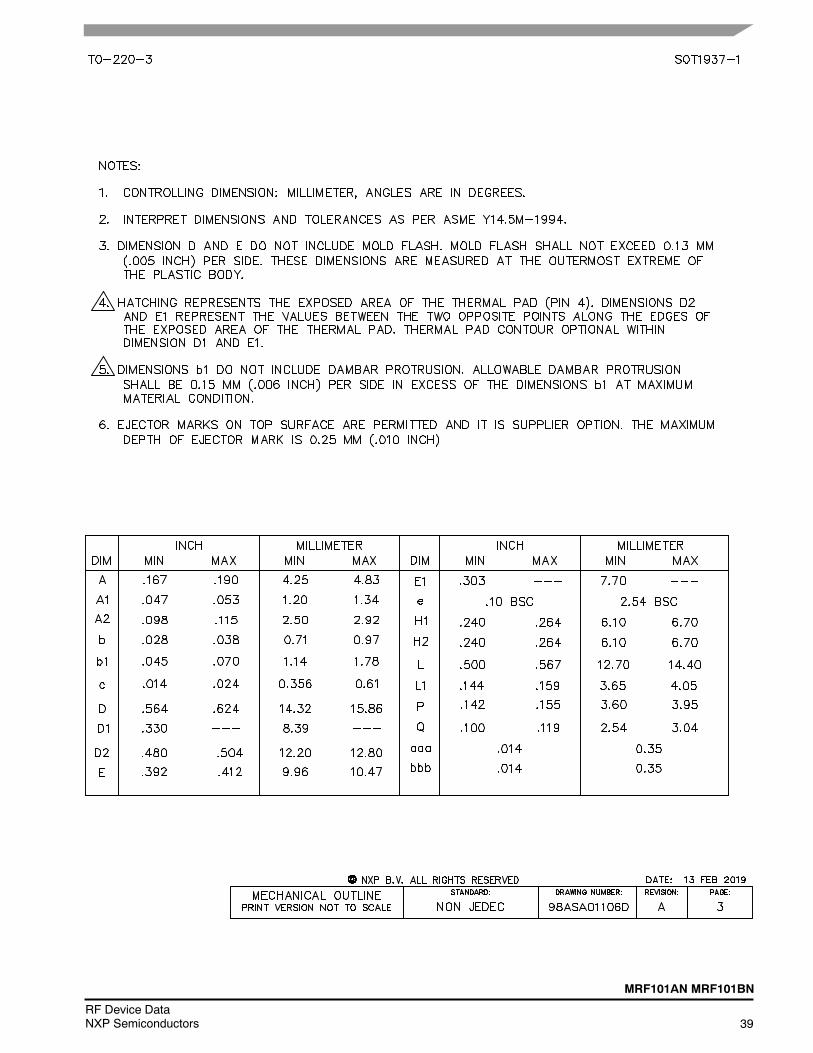
PACKAGE DIMENSIONS

38RF Device Data
NXP Semiconductors
MRF101AN MRF101BN
MRF101AN MRF101BN
39RF Device DataNXP Semiconductors
40RF Device Data
NXP Semiconductors
MRF101AN MRF101BN
PRODUCT DOCUMENTATION, SOFTWARE AND TOOLS
Refer to the following resources to aid your design process.
Application Notes AN1955: Thermal Measurement Methodology of RF Power Amplifiers
Engineering Bulletins EB212: Using Data Sheet Impedances for RF LDMOS Devices
Software Electromigration MTTF Calculator
RF High Power Model
.s2p File
Development Tools Printed Circuit Boards
Baseplate
To Download Resources Specific to a Given Part Number:1. Go to http://www.nxp.com/RF
2. Search by part number
3. Click part number link
4. Choose the desired resource from the drop down menu
REVISION HISTORY
The following table summarizes revisions to this document.
Revision Date Description
0 Nov. 2018 Initial release of data sheet
1 May 2019 Typical Performance table: updated values for 27 MHz, 50 MHz and 87.5–108 MHz reference circuits, p. 1
Load Mismatch/Ruggedness table, 40.68 MHz Pin: modulation signal corrected to CW, p. 1
Fig. 2, MTTF versus Junction Temperature — CW: added, p. 4
Added 13.56 MHz compact reference circuit, pp. 5–8
Added 27 MHz compact reference circuit, pp. 9–12
Table 13, row C12, C13: unit of measure/value in Description column changed from 10 nF to 0.01 F, p. 14
Added 50 MHz compact reference circuit, pp. 17–20
Added 81.36 MHz reference circuit, pp. 21–24
Added 87.5–108 MHz compact broadband reference circuit, pp. 25–29
Table 21, row C13: unit of measure/value in Description column changed from 10 nF to 0.01 F, p. 31
Fig. 42, CW Output Power versus Gate--Source Voltage at a Constant Input Power: added, p. 32
Package Outline Drawing: TO--220--3 package outline updated to Rev. A, pp. 37–39
MRF101AN MRF101BN
41RF Device DataNXP Semiconductors
How to Reach Us:
Home Page:nxp.com
Web Support:nxp.com/support
Information in this document is provided solely to enable system and softwareimplementers to use NXP products. There are no express or implied copyright licensesgranted hereunder to design or fabricate any integrated circuits based on the informationin this document. NXP reserves the right to make changes without further notice to anyproducts herein.
NXP makes no warranty, representation, or guarantee regarding the suitability of itsproducts for any particular purpose, nor does NXP assume any liability arising out of theapplication or use of any product or circuit, and specifically disclaims any and all liability,including without limitation consequential or incidental damages. “Typical” parametersthat may be provided in NXP data sheets and/or specifications can and do vary indifferent applications, and actual performance may vary over time. All operatingparameters, including “typicals,” must be validated for each customer application bycustomer’s technical experts. NXP does not convey any license under its patent rightsnor the rights of others. NXP sells products pursuant to standard terms and conditions ofsale, which can be found at the following address: nxp.com/SalesTermsandConditions.
NXP and the NXP logo are trademarks of NXP B.V. All other product or service namesare the property of their respective owners.E 2018–2019 NXP B.V.
Document Number: MRF101ANRev. 1, 05/2019
Related Documents