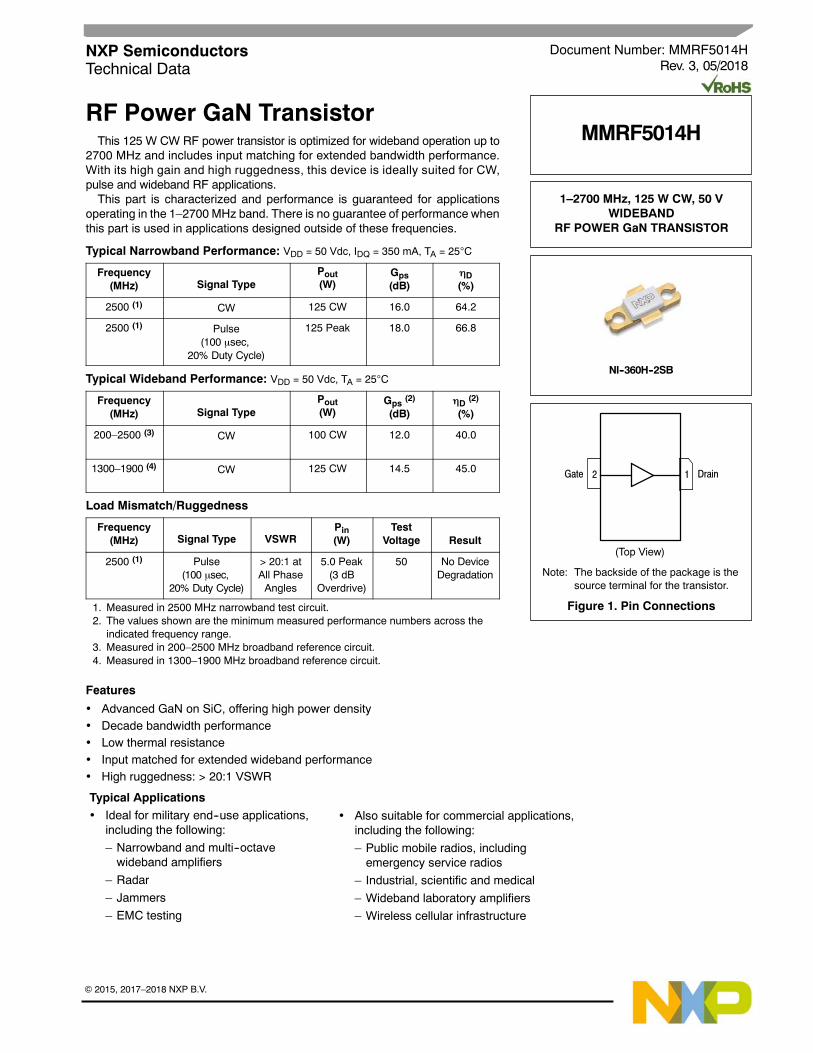
RF Power GaN Transistor This 125 W CW RF power transistor is optimized for wideband operation up to 2700 MHz and includes input matching for extended bandwidth performance. With its high gain and high ruggedness, this device is ideally suited for CW, pulse and wideband RF applications. This part is characterized and performance is guaranteed for applications operating in the 1–2700 MHz band. There is no guarantee of performance when this part is used in applications designed outside of these frequencies. Typical Narrowband Performance: V DD = 50 Vdc, I DQ = 350 mA, T A = 25C Frequency (MHz) Signal Type P out (W) G ps (dB) D (%) 2500 (1) CW 125 CW 16.0 64.2 2500 (1) Pulse (100 sec, 20% Duty Cycle) 125 Peak 18.0 66.8 Typical Wideband Performance: V DD = 50 Vdc, T A = 25C Frequency (MHz) Signal Type P out (W) G ps (2) (dB) D (2) (%) 200–2500 (3) CW 100 CW 12.0 40.0 1300–1900 (4) CW 125 CW 14.5 45.0 Load Mismatch/Ruggedness Frequency (MHz) Signal Type VSWR P in (W) Test Voltage Result 2500 (1) Pulse (100 sec, 20% Duty Cycle) > 20:1 at All Phase Angles 5.0 Peak (3 dB Overdrive) 50 No Device Degradation 1. Measured in 2500 MHz narrowband test circuit. 2. The values shown are the minimum measured performance numbers across the indicated frequency range. 3. Measured in 200–2500 MHz broadband reference circuit. 4. Measured in 1300–1900 MHz broadband reference circuit. Features Advanced GaN on SiC, offering high power density Decade bandwidth performance Low thermal resistance Input matched for extended wideband performance High ruggedness: > 20:1 VSWR Typical Applications Ideal for military end--use applications, including the following: – Narrowband and multi--octave wideband amplifiers – Radar – Jammers – EMC testing Also suitable for commercial applications, including the following: – Public mobile radios, including emergency service radios – Industrial, scientific and medical – Wideband laboratory amplifiers – Wireless cellular infrastructure Document Number: MMRF5014H Rev. 3, 05/2018 NXP Semiconductors Technical Data 1–2700 MHz, 125 W CW, 50 V WIDEBAND RF POWER GaN TRANSISTOR MMRF5014H NI--360H--2SB Note: The backside of the package is the source terminal for the transistor. (Top View) Drain 2 1 Figure 1. Pin Connections Gate 2015, 2017–2018 NXP B.V.

Welcome message from author
This document is posted to help you gain knowledge. Please leave a comment to let me know what you think about it! Share it to your friends and learn new things together.
Transcript
MMRF5014H
1RF Device DataNXP Semiconductors
RF Power GaN TransistorThis 125 W CW RF power transistor is optimized for wideband operation up to
2700 MHz and includes input matching for extended bandwidth performance.With its high gain and high ruggedness, this device is ideally suited for CW,pulse and wideband RF applications.This part is characterized and performance is guaranteed for applications
operating in the 1–2700 MHz band. There is no guarantee of performance whenthis part is used in applications designed outside of these frequencies.
Typical Narrowband Performance: VDD = 50 Vdc, IDQ = 350 mA, TA = 25C
Frequency(MHz) Signal Type
Pout(W)
Gps(dB)
D(%)
2500 (1) CW 125 CW 16.0 64.2
2500 (1) Pulse(100 sec,
20% Duty Cycle)
125 Peak 18.0 66.8
Typical Wideband Performance: VDD = 50 Vdc, TA = 25C
Frequency(MHz) Signal Type
Pout(W)
Gps(2)
(dB)D (2)
(%)
200–2500 (3) CW 100 CW 12.0 40.0
1300–1900 (4) CW 125 CW 14.5 45.0
Load Mismatch/Ruggedness
Frequency(MHz) Signal Type VSWR
Pin(W)
TestVoltage Result
2500 (1) Pulse(100 sec,
20% Duty Cycle)
> 20:1 atAll PhaseAngles
5.0 Peak(3 dB
Overdrive)
50 No DeviceDegradation
1. Measured in 2500 MHz narrowband test circuit.2. The values shown are the minimum measured performance numbers across the
indicated frequency range.3. Measured in 200–2500 MHz broadband reference circuit.4. Measured in 1300–1900 MHz broadband reference circuit.
Features
Advanced GaN on SiC, offering high power density Decade bandwidth performance Low thermal resistance Input matched for extended wideband performance High ruggedness: > 20:1 VSWR
Typical Applications Ideal for military end--use applications,
including the following:
– Narrowband and multi--octavewideband amplifiers
– Radar
– Jammers
– EMC testing
Also suitable for commercial applications,including the following:
– Public mobile radios, includingemergency service radios
– Industrial, scientific and medical
– Wideband laboratory amplifiers
– Wireless cellular infrastructure
Document Number: MMRF5014HRev. 3, 05/2018
NXP SemiconductorsTechnical Data
1–2700 MHz, 125 W CW, 50 VWIDEBAND
RF POWER GaN TRANSISTOR
MMRF5014H
NI--360H--2SB
Note: The backside of the package is thesource terminal for the transistor.
(Top View)
Drain2 1
Figure 1. Pin Connections
Gate
2015, 2017–2018 NXP B.V.

2RF Device Data
NXP Semiconductors
MMRF5014H
Table 1. Maximum RatingsRating Symbol Value Unit
Drain--Source Voltage VDSS 125 Vdc
Gate--Source Voltage VGS –8, 0 Vdc
Operating Voltage VDD 0 to +50 Vdc
Maximum Forward Gate Current @ TC = 25C IGMAX 18 mA
Storage Temperature Range Tstg –65 to +150 C
Case Operating Temperature Range TC –55 to +150 C
Operating Junction Temperature Range TJ –55 to +225 C
Absolute Maximum Channel Temperature (1) TMAX 350 C
Total Device Dissipation @ TC = 25CDerate above 25C
PD 2321.16
WW/C
Table 2. Thermal CharacteristicsCharacteristic Symbol Value Unit
Thermal Resistance by Infrared Measurement, Active Die Surface--to--CaseCW: Case Temperature 82C, 125 W CW, 50 Vdc, IDQ = 350 mA, 2500 MHz
RJC (IR) 0.86 (2) C/W
Thermal Resistance by Finite Element Analysis, Channel--to--CaseCase Temperature 85C, PD = 85 W
RCHC(FEA)
1.48 (3) C/W
Thermal Impedance by Infrared Measurement, Junction--to--CasePulse: Case Temperature 58C, 125 W Peak, 100 sec Pulse Width,20% Duty Cycle, 50 Vdc, IDQ = 350 mA, 2500 MHz
ZJC (IR) 0.21 C/W
Table 3. ESD Protection CharacteristicsTest Methodology Class
Human Body Model (per JESD22--A114) 1B, passes 500 V
Machine Model (per EIA/JESD22--A115) A, passes 100 V
Charge Device Model (per JESD22--C101) IV, passes 2000 V
Table 4. Electrical Characteristics (TA = 25C unless otherwise noted)
Characteristic Symbol Min Typ Max Unit
Off Characteristics
Drain Leakage Current(VGS = –8 Vdc, VDS = 10 Vdc)
IDSS — — 5 mAdc
Drain--Source Breakdown Voltage(VGS = –8 Vdc, ID = 25 mAdc)
V(BR)DSS 150 — — Vdc
On Characteristics
Gate Threshold Voltage(VDS = 10 Vdc, ID = 25 mAdc)
VGS(th) –3.8 –2.9 –2.3 Vdc
Gate Quiescent Voltage(VDS = 50 Vdc, ID = 350 mAdc, Measured in Functional Test)
VGS(Q) –3.2 –2.7 –2.2 Vdc
Dynamic Characteristics
Reverse Transfer Capacitance(VDS = 50 Vdc 30 mV(rms)ac @ 1 MHz, VGS = –4 Vdc)
Crss — 1.0 — pF
Output Capacitance(VDS = 50 Vdc 30 mV(rms)ac @ 1 MHz, VGS = –4 Vdc)
Coss — 7.7 — pF
Input Capacitance (4)
(VDS = 50 Vdc, VGS = –4 Vdc 30 mV(rms)ac @ 1 MHz)Ciss — 51.0 — pF
1. Reliability tests were conducted at 225C. Operation with TMAX at 350C will reduce median time to failure.2. Refer to AN1955, Thermal Measurement Methodology of RF Power Amplifiers. Go to http://www.nxp.com/RF and search for AN1955.3. RJC (FEA) must be used for purposes related to reliability and limitations on maximum junction temperature. MTTF may be estimated by
the expression MTTF (hours) = 10[A + B/(T + 273)], where T is the junction temperature in degrees Celsius, A = –8.44 and B = 7210.4. Part internally input matched.
(continued)

MMRF5014H
3RF Device DataNXP Semiconductors
Table 4. Electrical Characteristics (TA = 25C unless otherwise noted) (continued)
Characteristic Symbol Min Typ Max Unit
Functional Tests (In NXP Test Fixture, 50 ohm system) VDD = 50 Vdc, IDQ = 350 mA, Pout = 125 W Peak (25 W Avg.), f = 2500 MHz, 100sec Pulse Width, 20% Duty Cycle. [See note on correct biasing sequence.]
Power Gain Gps 17.0 18.0 20.0 dB
Drain Efficiency D 64.3 66.8 — %
Input Return Loss IRL — –12 –9 dB
Load Mismatch/Ruggedness (In NXP Test Fixture, 50 ohm system) IDQ = 350 mA
Frequency(MHz) Signal Type VSWR
Pin(W) Test Voltage, VDD Result
2500 Pulse(100 sec,
20% Duty Cycle)
> 20:1 at All Phase Angles 5.0 Peak(3 dB Overdrive)
50 No Device Degradation
Table 5. Ordering Information
Device Tape and Reel Information Package
MMRF5014HR5 R5 Suffix = 50 Units, 32 mm Tape Width, 13--inch Reel NI--360H--2SB
NOTE: Correct Biasing Sequence for GaN Depletion Mode Transistors
Turning the device ON1. Set VGS to –5 V
2. Turn on VDS to nominal supply voltage (50 V)
3. Increase VGS until IDS current is attained
4. Apply RF input power to desired level
Turning the device OFF1. Turn RF power off
2. Reduce VGS down to –5 V
3. Reduce VDS down to 0 V (Adequate time must be allowedfor VDS to reduce to 0 V to prevent severe damage to device.)
4. Turn off VGS
4RF Device Data
NXP Semiconductors
MMRF5014H
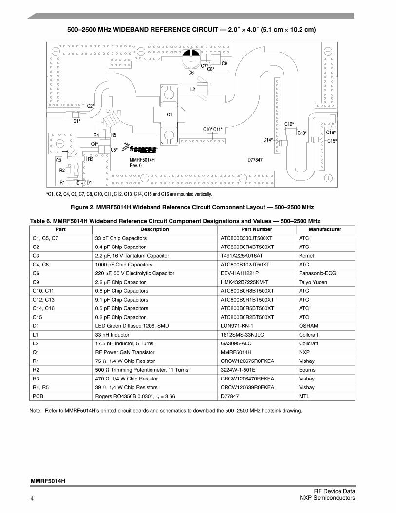
500–2500 MHz WIDEBAND REFERENCE CIRCUIT — 2.0 4.0 (5.1 cm 10.2 cm)
Figure 2. MMRF5014H Wideband Reference Circuit Component Layout — 500–2500 MHz
*C1, C2, C4, C5, C7, C8, C10, C11, C12, C13, C14, C15 and C16 are mounted vertically.
R1
MMRF5014H
D1
R2
C3 R3
C4*C5*
R4 R5
C1*
C2*L1
L2
Q1
C10* C11*
C6C7*
C8*
C12*
C13*C14* C15*
C16*
D77847
+
C9
Rev. 0
Table 6. MMRF5014H Wideband Reference Circuit Component Designations and Values — 500–2500 MHzPart Description Part Number Manufacturer
C1, C5, C7 33 pF Chip Capacitors ATC800B330JT500XT ATC
C2 0.4 pF Chip Capacitor ATC800B0R4BT500XT ATC
C3 2.2 F, 16 V Tantalum Capacitor T491A225K016AT Kemet
C4, C8 1000 pF Chip Capacitors ATC800B102JT50XT ATC
C6 220 F, 50 V Electrolytic Capacitor EEV-HA1H221P Panasonic-ECG
C9 2.2 F Chip Capacitor HMK432B7225KM-T Taiyo Yuden
C10, C11 0.8 pF Chip Capacitors ATC800B0R8BT500XT ATC
C12, C13 9.1 pF Chip Capacitors ATC800B9R1BT500XT ATC
C14, C16 0.5 pF Chip Capacitors ATC800B0R5BT500XT ATC
C15 0.2 pF Chip Capacitor ATC800B0R2BT500XT ATC
D1 LED Green Diffused 1206, SMD LGN971-KN-1 OSRAM
L1 33 nH Inductor 1812SMS-33NJLC Coilcraft
L2 17.5 nH Inductor, 5 Turns GA3095-ALC Coilcraft
Q1 RF Power GaN Transistor MMRF5014H NXP
R1 75 , 1/4 W Chip Resistor CRCW120675R0FKEA Vishay
R2 500 Trimming Potentiometer, 11 Turns 3224W-1-501E Bourns
R3 470 , 1/4 W Chip Resistor CRCW1206470RFKEA Vishay
R4, R5 39 , 1/4 W Chip Resistors CRCW120639R0FKEA Vishay
PCB Rogers RO4350B 0.030, r = 3.66 D77847 MTL
Note: Refer to MMRF5014H’s printed circuit boards and schematics to download the 500–2500 MHz heatsink drawing.

MMRF5014H
5RF Device DataNXP Semiconductors
TYPICAL CHARACTERISTICS — 500–2500 MHzWIDEBAND REFERENCE CIRCUIT
Figure 3. 500–2500 MHz Wideband Circuit Performance
f, FREQUENCY (MHz)
Gps,POWER
GAIN(dB)
11
400
20
22
21
100 W
Gps
17
19
18
10
70
D,DRAINEFFICIENCY(%)
800
20
30
40
50
60
D
10 W
100 W
VDD = 50 Vdc, IDQ = 300 mA, CW
12
14
13
15
16
600 1000 1200 1400 1600
15
25
35
45
55
65
1800 2000 2200 2400 260010
6RF Device Data
NXP Semiconductors
MMRF5014H
200–2500 MHz WIDEBAND REFERENCE CIRCUIT — 4.0 5.0 (10.2 cm 12.7 cm)
Figure 4. MMRF5014H Wideband Reference Circuit Component Layout — 200–2500 MHz
**C1, C2, C3, C6, C12, C13, C15, C16, C17, R1, and R2 are mounted vertically.**Stacked
MMRF5014HRev. 6
VGG
VDD
C1**
R2**
R1**
C2* C3*
C4 C7 C8
C6*
C5
L1
R3 R4
C9 C10
C11C12*
L2C13*
C14
C15*C16*C17*
B1 B2T2
T1
D68303
Q1
C15*
C16*
C17*B1 B2
T2
T1
T2
T1
B1
Detail BB 2X
SeeDetail BB
Section AA
Section AA
T2
MMRF5014H
7RF Device DataNXP Semiconductors
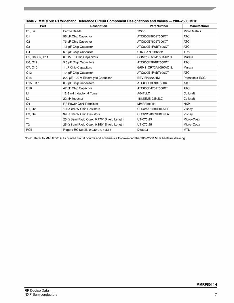
Table 7. MMRF5014H Wideband Reference Circuit Component Designations and Values — 200–2500 MHzPart Description Part Number Manufacturer
B1, B2 Ferrite Beads T22-6 Micro Metals
C1 56 pF Chip Capacitor ATC800B560JT500XT ATC
C2 75 pF Chip Capacitor ATC800B750JT500XT ATC
C3 1.6 pF Chip Capacitor ATC800B1R6BT500XT ATC
C4 6.8 F Chip Capacitor C4532X7R1H685K TDK
C5, C8, C9, C11 0.015 F Chip Capacitors GRM319R72A153KA01D Murata
C6, C12 5.6 pF Chip Capacitors ATC800B5R6BT500XT ATC
C7, C10 1 F Chip Capacitors GRM31CR72A105KAO1L Murata
C13 1.4 pF Chip Capacitor ATC800B1R4BT500XT ATC
C14 220 F, 100 V Electrolytic Capacitor EEV-FK2A221M Panasonic-ECG
C15, C17 0.9 pF Chip Capacitors ATC800B0R9BT500XT ATC
C16 47 pF Chip Capacitor ATC800B470JT500XT ATC
L1 12.5 nH Inductor, 4 Turns A04TJLC Coilcraft
L2 22 nH Inductor 1812SMS-22NJLC Coilcraft
Q1 RF Power GaN Transistor MMRF5014H NXP
R1, R2 10 , 3/4 W Chip Resistors CRCW201010R0FKEF Vishay
R3, R4 39 , 1/4 W Chip Resistors CRCW120639R0FKEA Vishay
T1 25 Semi Rigid Coax, 0.770 Shield Length UT-070-25 Micro--Coax
T2 25 Semi Rigid Coax, 0.850 Shield Length UT-070-25 Micro--Coax
PCB Rogers RO4350B, 0.030, r = 3.66 D68303 MTL
Note: Refer to MMRF5014H’s printed circuit boards and schematics to download the 200–2500 MHz heatsink drawing.
8RF Device Data
NXP Semiconductors
MMRF5014H
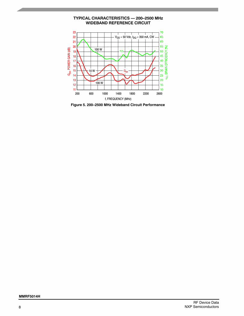
TYPICAL CHARACTERISTICS — 200–2500 MHzWIDEBAND REFERENCE CIRCUIT
Figure 5. 200–2500 MHz Wideband Circuit Performance
f, FREQUENCY (MHz)
Gps,POWER
GAIN(dB)
11
23
200
20
22
21
100 W
Gps
17
19
18
10
70
D,DRAINEFFICIENCY(%)
1000
20
30
40
50
60
D
10 W
100 W
VDD = 50 Vdc, IDQ = 350 mA, CW
12
14
13
1516
600 1400 1800 2200 2600
15
25
35
45
55
65
MMRF5014H
9RF Device DataNXP Semiconductors
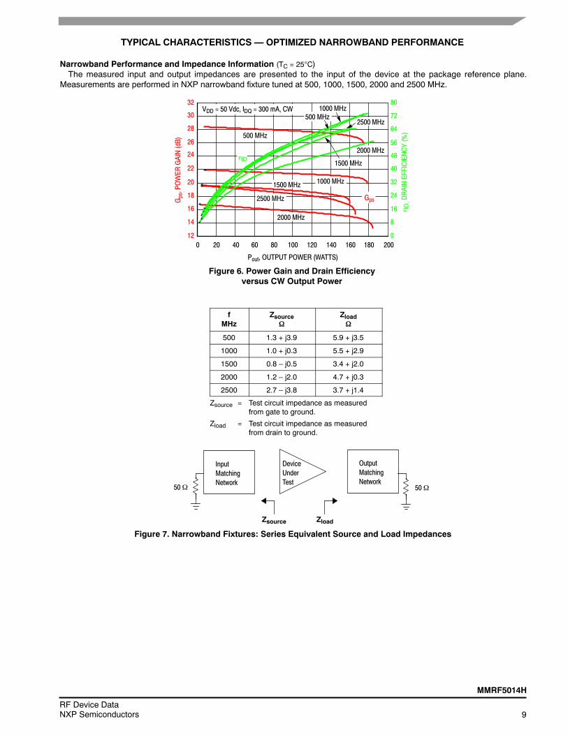
TYPICAL CHARACTERISTICS — OPTIMIZED NARROWBAND PERFORMANCE
Narrowband Performance and Impedance Information (TC = 25C)The measured input and output impedances are presented to the input of the device at the package reference plane.
Measurements are performed in NXP narrowband fixture tuned at 500, 1000, 1500, 2000 and 2500 MHz.
Figure 6. Power Gain and Drain Efficiencyversus CW Output Power
Pout, OUTPUT POWER (WATTS)
Gps,POWER
GAIN(dB)
12
32
0
26
30
28
Gps
20
24
22
0
80
D,DRAINEFFICIENCY(%)
40
16
32
48
64
1000 MHzVDD = 50 Vdc, IDQ = 300 mA, CW
14
16
18
20 60 200
8
24
56
72
80 100 120 140 160 180
40
500 MHz
500 MHz
2000 MHz
1500 MHz
2500 MHz
1000 MHz1500 MHz
2500 MHz
2000 MHz
D
fMHz
Zsource
Zload
500 1.3 + j3.9 5.9 + j3.5
1000 1.0 + j0.3 5.5 + j2.9
1500 0.8 – j0.5 3.4 + j2.0
2000 1.2 – j2.0 4.7 + j0.3
2500 2.7 – j3.8 3.7 + j1.4
Zsource = Test circuit impedance as measuredfrom gate to ground.
Zload = Test circuit impedance as measuredfrom drain to ground.
Figure 7. Narrowband Fixtures: Series Equivalent Source and Load Impedances
5050
InputMatchingNetwork
DeviceUnderTest
OutputMatchingNetwork
Zsource Zload
10RF Device Data
NXP Semiconductors
MMRF5014H
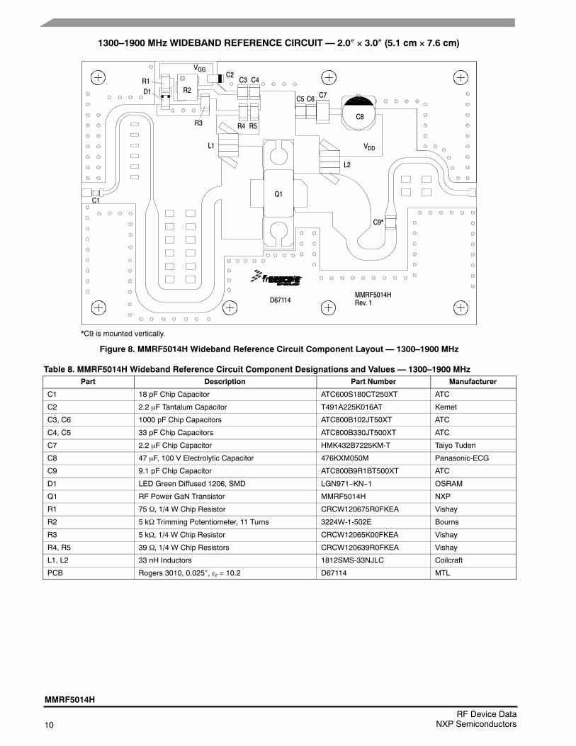
1300–1900 MHz WIDEBAND REFERENCE CIRCUIT — 2.0 3.0 (5.1 cm 7.6 cm)
Figure 8. MMRF5014H Wideband Reference Circuit Component Layout — 1300–1900 MHz
*C9 is mounted vertically.
MMRF5014HRev. 1
VGG
VDD
D67114
C9*
R1R2
R3 R4 R5
C1
C2C3 C4
C5 C6 C7
C8
Q1
L1
L2
D1
Table 8. MMRF5014H Wideband Reference Circuit Component Designations and Values — 1300–1900 MHzPart Description Part Number Manufacturer
C1 18 pF Chip Capacitor ATC600S180CT250XT ATC
C2 2.2 F Tantalum Capacitor T491A225K016AT Kemet
C3, C6 1000 pF Chip Capacitors ATC800B102JT50XT ATC
C4, C5 33 pF Chip Capacitors ATC800B330JT500XT ATC
C7 2.2 F Chip Capacitor HMK432B7225KM-T Taiyo Tuden
C8 47 F, 100 V Electrolytic Capacitor 476KXM050M Panasonic-ECG
C9 9.1 pF Chip Capacitor ATC800B9R1BT500XT ATC
D1 LED Green Diffused 1206, SMD LGN971--KN--1 OSRAM
Q1 RF Power GaN Transistor MMRF5014H NXP
R1 75 , 1/4 W Chip Resistor CRCW120675R0FKEA Vishay
R2 5 k Trimming Potentiometer, 11 Turns 3224W-1-502E Bourns
R3 5 k, 1/4 W Chip Resistor CRCW12065K00FKEA Vishay
R4, R5 39 , 1/4 W Chip Resistors CRCW120639R0FKEA Vishay
L1, L2 33 nH Inductors 1812SMS-33NJLC Coilcraft
PCB Rogers 3010, 0.025, r = 10.2 D67114 MTL

MMRF5014H
11RF Device DataNXP Semiconductors
TYPICAL CHARACTERISTICS — 1300–1900 MHzWIDEBAND REFERENCE CIRCUIT
Figure 9. Power Gain and Drain Efficiencyversus Frequency
f, FREQUENCY (MHz)
Gps,POWER
GAIN(dB)
12
1300
26
30
28
Gps
20
24
22
30
70
D,DRAINEFFICIENCY(%)
38
46
54
62
D
VDD = 50 Vdc, IDQ = 200 mA, Pout = 125 W, CW
14
16
18
1900
34
42
58
66
50
101400 1500 1600 1700 1800
Figure 10. Power Gain and Drain Efficiencyversus CW Output Power
Pout, OUTPUT POWER (WATTS)
Gps,POWER
GAIN(dB)
0
20
0
14
18
16
Gps
8
12
10
25
75
D,DRAINEFFICIENCY(%)
40
35
45
55
65
D
VDD = 50 Vdc, IDQ = 200 mA, CW
2
4
6
20 60 180
30
40
60
70
80 100 120 140 160
501300 MHz
1600 MHz1900 MHz
1900 MHz
1600 MHz1300 MHz
12RF Device Data
NXP Semiconductors
MMRF5014H
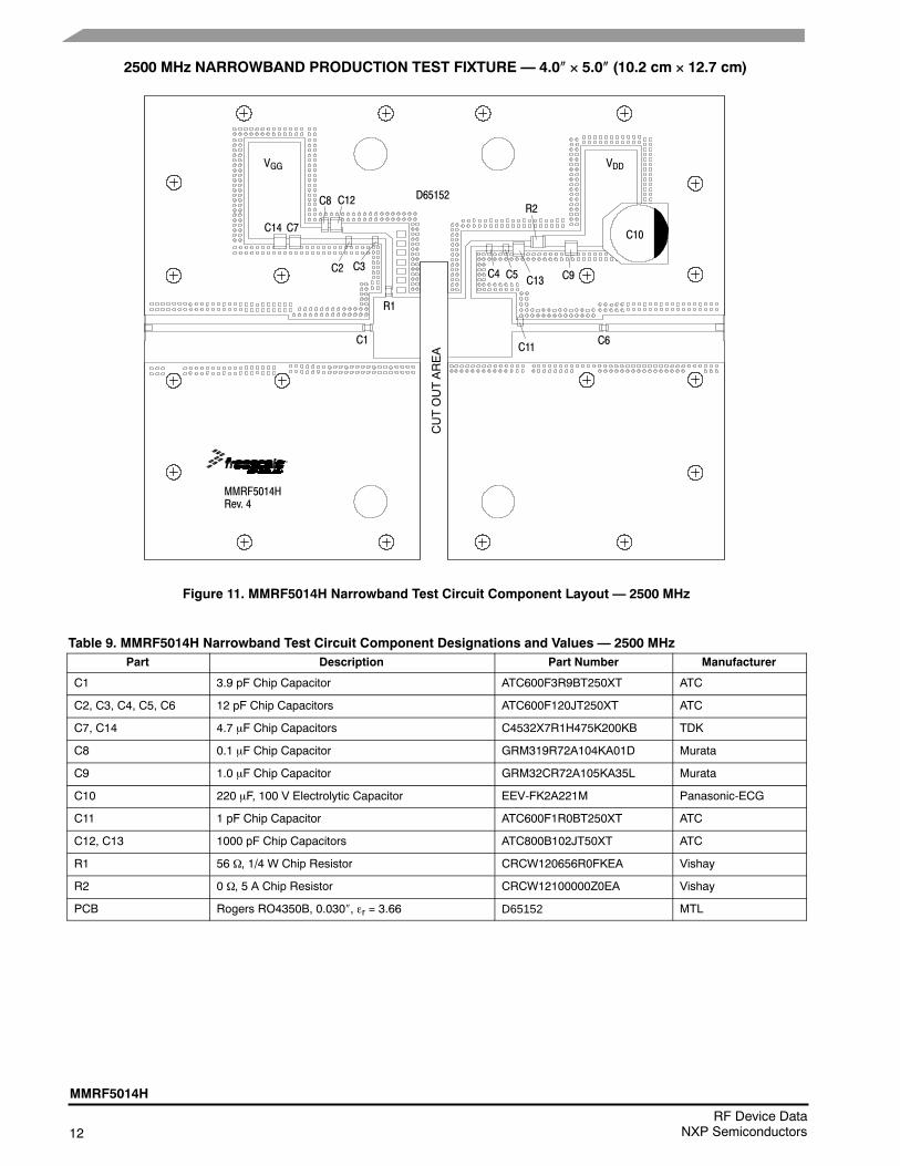
2500 MHz NARROWBAND PRODUCTION TEST FIXTURE — 4.0 5.0 (10.2 cm 12.7 cm)
Figure 11. MMRF5014H Narrowband Test Circuit Component Layout — 2500 MHz
MMRF5014HRev. 4
CUTOUTAREA
C14 C7
C8 C12
C2 C3
R1
C1
C4 C5 C13 C9
C11C6
C10
VDDVGG
D65152R2
Table 9. MMRF5014H Narrowband Test Circuit Component Designations and Values — 2500 MHzPart Description Part Number Manufacturer
C1 3.9 pF Chip Capacitor ATC600F3R9BT250XT ATC
C2, C3, C4, C5, C6 12 pF Chip Capacitors ATC600F120JT250XT ATC
C7, C14 4.7 F Chip Capacitors C4532X7R1H475K200KB TDK
C8 0.1 F Chip Capacitor GRM319R72A104KA01D Murata
C9 1.0 F Chip Capacitor GRM32CR72A105KA35L Murata
C10 220 F, 100 V Electrolytic Capacitor EEV-FK2A221M Panasonic-ECG
C11 1 pF Chip Capacitor ATC600F1R0BT250XT ATC
C12, C13 1000 pF Chip Capacitors ATC800B102JT50XT ATC
R1 56 , 1/4 W Chip Resistor CRCW120656R0FKEA Vishay
R2 0 , 5 A Chip Resistor CRCW12100000Z0EA Vishay
PCB Rogers RO4350B, 0.030, r = 3.66 D65152 MTL
MMRF5014H
13RF Device DataNXP Semiconductors
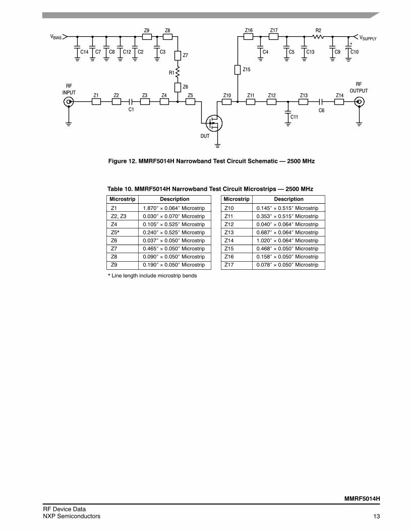
Figure 12. MMRF5014H Narrowband Test Circuit Schematic — 2500 MHz
Z1
RFINPUT
C1
Z2 Z3 Z4 Z5
DUT
Z13
C6
RFOUTPUT
VBIAS VSUPPLY
C9 C10C5C14 C8
Z9
Z14
C11
R1
+
Z7C7
Z12
C2C12 C3
Z8
Z6
Z10 Z11
Z15
C13
Z17
C4
Z16
DescriptionMicrostripDescriptionMicrostrip
Z1 1.870 0.064 Microstrip
Z2, Z3 0.030 0.070 Microstrip
Z4 0.105 0.525 Microstrip
Z5* 0.240 0.525 Microstrip
Z6 0.037 0.050 Microstrip
Z7 0.465 0.050 Microstrip
Z8 0.090 0.050 Microstrip
Z9 0.190 0.050 Microstrip
* Line length include microstrip bends
Z10 0.145 0.515 Microstrip
Z11 0.353 0.515 Microstrip
Z12 0.040 0.064 Microstrip
Z13 0.687 0.064 Microstrip
Z14 1.020 0.064 Microstrip
Z15 0.468 0.050 Microstrip
Z16 0.158 0.050 Microstrip
Z17 0.078 0.050 Microstrip
Table 10. MMRF5014H Narrowband Test Circuit Microstrips — 2500 MHz
R2
14RF Device Data
NXP Semiconductors
MMRF5014H
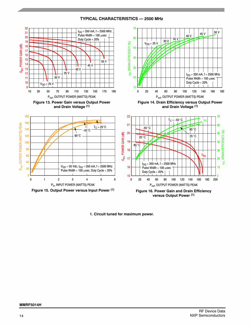
TYPICAL CHARACTERISTICS — 2500 MHz
9
22
10
Pout, OUTPUT POWER (WATTS) PEAK
Figure 13. Power Gain versus Output Powerand Drain Voltage (1)
Gps,POWER
GAIN(dB)
30
20
150 190
18
50 70 90 130
VDD = 25 V
50 V
17
19
21
45 V
110 170
1514
16
1211
13
10
IDQ = 350 mA, f = 2500 MHzPulse Width = 100 secDuty Cycle = 20%
30 V35 V
40 V
10
70
0
Pout, OUTPUT POWER (WATTS) PEAK
Figure 14. Drain Efficiency versus Output Powerand Drain Voltage (1)
D,DRAINEFFICIENCY(%)
20
60
140 180
50
40 60 80 120
VDD = 25 V
50 V
40
45 V
100 160
30
20IDQ = 350 mA, f = 2500 MHzPulse Width = 100 secDuty Cycle = 20%
30 V35 V
40 V
0
180
0
Pin, INPUT POWER (WATTS) PEAK
Figure 15. Output Power versus Input Power (1)
P out,OUTPUTPOWER
(WATTS)PEAK
2
160
6
140
3 4 5
TC = 25C
120
100
20VDD = 50 Vdc, IDQ = 350 mA, f = 2500 MHzPulse Width = 100 sec, Duty Cycle = 20%
40
60
80
1
85C
–55C
Figure 16. Power Gain and Drain Efficiencyversus Output Power (1)
Pout, OUTPUT POWER (WATTS) PEAK
Gps,POWER
GAIN(dB)
15
22
0
19
21
20
100 200
25_C
85_C
Gps
16
18
17
0
70
10
D,DRAINEFFICIENCY(%)85_C
25_C
20
20
30
40
50
60
IDQ = 350 mA, f = 2500 MHzPulse Width = 100 secDuty Cycle = 20%
D
–55_C
TC = –55_C
40 60 80 140120 180160
1. Circuit tuned for maximum power.
MMRF5014H
15RF Device DataNXP Semiconductors
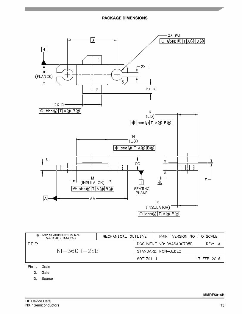
PACKAGE DIMENSIONS
Pin 1. Drain
2. Gate
3. Source

16RF Device Data
NXP Semiconductors
MMRF5014H
MMRF5014H
17RF Device DataNXP Semiconductors
PRODUCT DOCUMENTATION AND TOOLS
Refer to the following resources to aid your design process.
Application Notes AN1955: Thermal Measurement Methodology of RF Power Amplifiers
Development Tools Printed Circuit Boards
To Download Resources Specific to a Given Part Number:
1. Go to http://www.nxp.com/RF
2. Search by part number
3. Click part number link
4. Choose the desired resource from the drop down menu
REVISION HISTORY
The following table summarizes revisions to this document.
Revision Date Description
0 May 2015 Initial Release of Data Sheet
1 Sept. 2015 Table 1, Maximum Ratings: added Maximum Forward Gate Current, p. 2
Table 4, Electrical Characteristics: changed Load Mismatch/Ruggedness signal type to pulse to reflectcorrect modulation signal, p. 3
2 Apr. 2017 Biasing sequence for GaN depletion mode transistors: revised note to clarify correct biasing sequence forGaN parts, p. 3
500–2500 MHz wideband reference circuit: added performance data and graph, reference circuitcomponent layout and component designations, pp. 4–5
3 May 2018 Table 2, Thermal Characteristics: updated to include RCHC (FEA) data, p. 2

18RF Device Data
NXP Semiconductors
MMRF5014H
How to Reach Us:
Home Page:nxp.com
Web Support:nxp.com/support
Information in this document is provided solely to enable system and softwareimplementers to use NXP products. There are no express or implied copyright licensesgranted hereunder to design or fabricate any integrated circuits based on the informationin this document. NXP reserves the right to make changes without further notice to anyproducts herein.
NXP makes no warranty, representation, or guarantee regarding the suitability of itsproducts for any particular purpose, nor does NXP assume any liability arising out of theapplication or use of any product or circuit, and specifically disclaims any and all liability,including without limitation consequential or incidental damages. “Typical” parametersthat may be provided in NXP data sheets and/or specifications can and do vary indifferent applications, and actual performance may vary over time. All operatingparameters, including “typicals,” must be validated for each customer application bycustomer’s technical experts. NXP does not convey any license under its patent rightsnor the rights of others. NXP sells products pursuant to standard terms and conditions ofsale, which can be found at the following address: nxp.com/SalesTermsandConditions.
NXP, the NXP logo, Freescale, and the Freescale logo are trademarks of NXP B.V.All other product or service names are the property of their respective owners.E 2015, 2017–2018 NXP B.V.
Document Number: MMRF5014HRev. 3, 05/2018

Mouser Electronics
Authorized Distributor
Click to View Pricing, Inventory, Delivery & Lifecycle Information: NXP:
MMRF5014HR5 MMRF5014H-500MHZ MMRF5014H-200MHZ
Related Documents