4 GHz to 8.5 GHz, GaAs, MMIC, I/Q Mixer Data Sheet HMC525ALC4 Rev. A Document Feedback Information furnished by Analog Devices is believed to be accurate and reliable. However, no responsibility is assumed by Analog Devices for its use, nor for any infringements of patents or other rights of third parties that may result from its use. Specifications subject to change without notice. No license is granted by implication or otherwise under any patent or patent rights of Analog Devices. Trademarks and registered trademarks are the property of their respective owners. One Technology Way, P.O. Box 9106, Norwood, MA 02062-9106, U.S.A. Tel: 781.329.4700 ©2018 Analog Devices, Inc. All rights reserved. Technical Support www.analog.com FEATURES Passive: no dc bias required Conversion loss: 8 dB (typical) Input IP3: 20 dBm (typical) LO to RF isolation: 47 dB (typical) IF frequency range: dc to 3.5 GHz RoHS compliant, 24-terminal, 4 mm × 4 mm LCC package APPLICATIONS Microwave and very small aperture terminal radios Test equipment Point to point radios Military electronic warfare; electronic countermeasure; and command, control, communications, and intelligence FUNCTIONAL BLOCK DIAGRAM 13 1 3 4 2 7 NIC NIC GND RF 5 6 GND NIC NIC 14 GND 15 LO 16 GND 17 NIC 18 NIC NIC 8 NIC 9 IF1 10 NIC 11 IF2 12 19 GND GND NIC 20 NIC 21 NIC 22 NIC 23 NIC 24 NIC PACKAGE BASE 90° HYBRID HMC525ALC4 16401-001 Figure 1. GENERAL DESCRIPTION The HMC525ALC4 is a compact gallium arsenide (GaAs), monolithic microwave integrated circuit (MMIC), in phase quadrature (I/Q) mixer in a 24-terminal, RoHS compliant, ceramic leadless chip carrier (LCC) package. The device can be used as either an image reject mixer or a single sideband (SSB) upconverter. The mixer uses two standard double balanced mixer cells and a 90° hybrid fabricated in a GaAs, metal semiconductor field effect transistor (MESFET) process. The HMC525ALC4 is a much smaller alternative to a hybrid style image reject mixer and a SSB upconverter assembly. The HMC525ALC4 eliminates the need for wire bonding, allowing the use of surface-mount manufacturing techniques.

Welcome message from author
This document is posted to help you gain knowledge. Please leave a comment to let me know what you think about it! Share it to your friends and learn new things together.
Transcript

4 GHz to 8.5 GHz, GaAs, MMIC, I/Q Mixer
Data Sheet HMC525ALC4
Rev. A Document Feedback Information furnished by Analog Devices is believed to be accurate and reliable. However, no responsibility is assumed by Analog Devices for its use, nor for any infringements of patents or other rights of third parties that may result from its use. Specifications subject to change without notice. No license is granted by implication or otherwise under any patent or patent rights of Analog Devices. Trademarks and registered trademarks are the property of their respective owners.
One Technology Way, P.O. Box 9106, Norwood, MA 02062-9106, U.S.A. Tel: 781.329.4700 ©2018 Analog Devices, Inc. All rights reserved. Technical Support www.analog.com
FEATURES Passive: no dc bias required Conversion loss: 8 dB (typical) Input IP3: 20 dBm (typical) LO to RF isolation: 47 dB (typical) IF frequency range: dc to 3.5 GHz RoHS compliant, 24-terminal, 4 mm × 4 mm LCC package
APPLICATIONS Microwave and very small aperture terminal radios Test equipment Point to point radios Military electronic warfare; electronic countermeasure; and
command, control, communications, and intelligence
FUNCTIONAL BLOCK DIAGRAM
13
1
34
2
7
NICNIC
GNDRF
56
GNDNIC NIC
14 GND15 LO16 GND17 NIC18 NIC
NIC
8N
IC9
IF1
10N
IC11
IF2
1219
GN
D
GND
NIC
20N
IC21
NIC
22N
IC23
NIC
24N
IC
PACKAGEBASE
90° HYBRIDHMC525ALC4
1640
1-00
1
Figure 1.
GENERAL DESCRIPTION The HMC525ALC4 is a compact gallium arsenide (GaAs), monolithic microwave integrated circuit (MMIC), in phase quadrature (I/Q) mixer in a 24-terminal, RoHS compliant, ceramic leadless chip carrier (LCC) package. The device can be used as either an image reject mixer or a single sideband (SSB) upconverter. The mixer uses two standard double balanced
mixer cells and a 90° hybrid fabricated in a GaAs, metal semiconductor field effect transistor (MESFET) process. The HMC525ALC4 is a much smaller alternative to a hybrid style image reject mixer and a SSB upconverter assembly. The HMC525ALC4 eliminates the need for wire bonding, allowing the use of surface-mount manufacturing techniques.
HMC525ALC4 Data Sheet
Rev. A | Page 2 of 28
TABLE OF CONTENTS Features .............................................................................................. 1 Applications ....................................................................................... 1 Functional Block Diagram .............................................................. 1 General Description ......................................................................... 1 Revision History ............................................................................... 2 Specifications ..................................................................................... 3 Absolute Maximum Ratings ............................................................ 4
Thermal Resistance ...................................................................... 4 ESD Caution .................................................................................. 4
Pin Configuration and Function Descriptions ............................. 5 Interface Schematics..................................................................... 5
Typical Performance Characteristics ............................................. 6 Downconverter Performance ...................................................... 6
Upconverter Performance ......................................................... 12 Phase and Amplitude Balance—Downconverter................... 18 Isolation and Return Loss ......................................................... 20 IF Bandwidth—Downconverter ............................................... 22 Spurious and Harmonics Performance ................................... 24
Theory of Operation ...................................................................... 25 Applications Information .............................................................. 26
Typical Application Circuit ....................................................... 26 Evaluation PCB Information .................................................... 26 Soldering Information and Recommended Land Pattern .... 27
Outline Dimensions ....................................................................... 28 Ordering Guide .......................................................................... 28
REVISION HISTORY 5/2018—Rev. 0 to Rev. A Changes to Typical Application Circuit Section......................... 26 4/2018—Revision 0: Initial Version

Data Sheet HMC525ALC4
Rev. A | Page 3 of 28
SPECIFICATIONS LO = 15 dBm, intermediate frequency (IF) = 100 MHz, RF = −10 dBm, TA = 25°C, unless otherwise noted. All measurements were made as downconverter with lower sideband selected (high-side LO) and an external 90° IF hybrid at the IF ports, unless otherwise noted.
Table 1. Parameter Test Conditions/Comments Min Typ Max Unit FREQUENCY RANGE
RF 4 8.5 GHz LO Input 4 8.5 GHz IF DC 3.5 GHz
LO AMPLITUDE 13 15 17 dBm 4 GHz to 8.5 GHz PERFORMANCE
Downconverter Taken as image reject mixer Conversion Loss 8 11 dB Noise Figure 8 dB Input Third-Order Intercept (IP3) 17 20 dBm Input Power for 1dB Compression (P1dB) 13 dBm Image Rejection 23 30 dBc
Upconverter Taken as SSB upconverter mixer Conversion Loss 7.5 dB Input IP3 20 dBm Input P1dB 8.5 dBm Sideband Rejection 30 dBc
Isolation Taken without external 90° IF hybrid LO to RF 35 47 dB LO to IF 23 dB RF to IF 42 dB
Balance Taken without external 90° IF hybrid Phase 2 Degree Amplitude 0.05 dB
4.5 GHz to 6 GHz PERFORMANCE Downconverter Taken as image reject mixer
Conversion Loss 7.5 9.5 dB Noise Figure 7.5 dB Input IP3 17 21 dBm Input P1dB 12 dBm Image Rejection 25 30 dBc
Upconverter Taken as SSB upconverter mixer Conversion Loss 7 dB Input IP3 22 dBm Input P1dB 10.5 dBm Sideband Rejection 30 dBc
Isolation Taken without external 90° IF hybrid LO to RF 35 45 dB LO to IF 21 dB RF to IF 40 dB
Balance Taken without external 90° IF hybrid Phase 3 Degree Amplitude 0.15 dB
HMC525ALC4 Data Sheet
Rev. A | Page 4 of 28
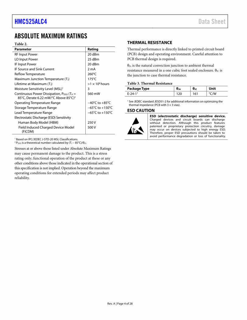
ABSOLUTE MAXIMUM RATINGS Table 2. Parameter Rating RF Input Power 20 dBm LO Input Power 25 dBm IF Input Power 20 dBm IF Source and Sink Current 2 mA Reflow Temperature 260°C Maximum Junction Temperature (TJ) 175°C Lifetime at Maximum (TJ) >1 × 10⁶ hours Moisture Sensitivity Level (MSL)1 3 Continuous Power Dissipation, PDISS (TA =
85°C, Derate 6.22 mW/°C Above 85°C)2 560 mW
Operating Temperature Range −40°C to +85°C Storage Temperature Range −65°C to +150°C Lead Temperature Range −65°C to +150°C Electrostatic Discharge (ESD) Sensitivity
Human Body Model (HBM) 250 V Field Induced Charged Device Model
(FICDM) 500 V
1 Based on IPC/JEDEC J-STD-20 MSL Classifications. 2 PDISS is a theoretical number calculated by (TJ − 85°C)/θJC.
Stresses at or above those listed under Absolute Maximum Ratings may cause permanent damage to the product. This is a stress rating only; functional operation of the product at these or any other conditions above those indicated in the operational section of this specification is not implied. Operation beyond the maximum operating conditions for extended periods may affect product reliability.
THERMAL RESISTANCE Thermal performance is directly linked to printed circuit board (PCB) design and operating environment. Careful attention to PCB thermal design is required.
θJA is the natural convection junction to ambient thermal resistance measured in a one cubic foot sealed enclosure. θJC is the junction to case thermal resistance.
Table 3. Thermal Resistance Package Type θJA θJC Unit E-24-11 120 161 °C/W
1 See JEDEC standard JESD51-2 for additional information on optimizing the thermal impedance (PCB with 3 × 3 vias).
ESD CAUTION
Data Sheet HMC525ALC4
Rev. A | Page 5 of 28
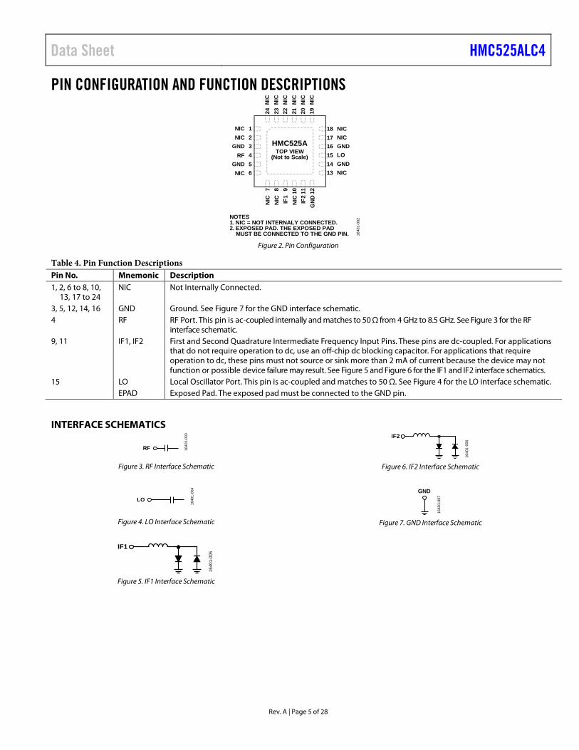
PIN CONFIGURATION AND FUNCTION DESCRIPTIONS
13
1
34
2
7
NICNIC
GNDRF
56
GNDNIC NIC
14 GND15 LO16 GND17 NIC18 NIC
NIC
8N
IC9
IF1
10N
IC11
IF2
1219
GN
DN
IC20
NIC
21N
IC22
NIC
23N
IC24
NIC
HMC525ATOP VIEW
(Not to Scale)
NOTES1. NIC = NOT INTERNALY CONNECTED.2. EXPOSED PAD. THE EXPOSED PAD
MUST BE CONNECTED TO THE GND PIN. 1640
1-00
2
Figure 2. Pin Configuration
Table 4. Pin Function Descriptions Pin No. Mnemonic Description 1, 2, 6 to 8, 10,
13, 17 to 24 NIC Not Internally Connected.
3, 5, 12, 14, 16 GND Ground. See Figure 7 for the GND interface schematic. 4 RF RF Port. This pin is ac-coupled internally and matches to 50 Ω from 4 GHz to 8.5 GHz. See Figure 3 for the RF
interface schematic. 9, 11 IF1, IF2 First and Second Quadrature Intermediate Frequency Input Pins. These pins are dc-coupled. For applications
that do not require operation to dc, use an off-chip dc blocking capacitor. For applications that require operation to dc, these pins must not source or sink more than 2 mA of current because the device may not function or possible device failure may result. See Figure 5 and Figure 6 for the IF1 and IF2 interface schematics.
15 LO Local Oscillator Port. This pin is ac-coupled and matches to 50 Ω. See Figure 4 for the LO interface schematic. EPAD Exposed Pad. The exposed pad must be connected to the GND pin.
INTERFACE SCHEMATICS
RF 1640
1-00
3
Figure 3. RF Interface Schematic
LO
1640
1-00
4
Figure 4. LO Interface Schematic
IF1
1640
1-00
5
Figure 5. IF1 Interface Schematic
IF2
1640
1-00
6
Figure 6. IF2 Interface Schematic
GND
1640
1-00
7
Figure 7. GND Interface Schematic
HMC525ALC4 Data Sheet
Rev. A | Page 6 of 28
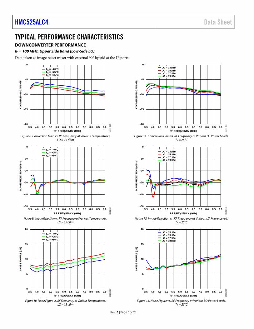
TYPICAL PERFORMANCE CHARACTERISTICS DOWNCONVERTER PERFORMANCE IF = 100 MHz, Upper Side Band (Low-Side LO)
Data taken as image reject mixer with external 90° hybrid at the IF ports.
–20
–15
–10
–5
0
3.5 4.0 4.5 5.0 5.5 6.0 6.5 7.0 7.5 8.0 8.5 9.0
CO
NVE
RSI
ON
GA
IN (d
B)
RF FREQUENCY (GHz)
TA = –40°CTA = +25°CTA = +85°C
1640
1-00
8
Figure 8. Conversion Gain vs. RF Frequency at Various Temperatures,
LO = 15 dBm
–50
–40
–20
–30
–10
0
3.5 4.0 4.5 5.0 5.5 6.0 6.5 7.0 7.5 8.0 8.5 9.0
IMA
GE
REJ
ECTI
ON
(dB
c)
RF FREQUENCY (GHz)
TA = –40°CTA = +25°CTA = +85°C
1640
1-00
9
Figure 9. Image Rejection vs. RF Frequency at Various Temperatures,
LO = 15 dBm
0
5
10
15
20
3.5 4.0 4.5 5.0 5.5 6.0 6.5 7.0 7.5 8.0 8.5 9.0
NO
ISE
FIG
UR
E (d
B)
RF FREQUENCY (GHz) 1640
1-01
3
TA = –40°CTA = +25°CTA = +85°C
Figure 10. Noise Figure vs. RF Frequency at Various Temperatures,
LO = 15 dBm
–20
–15
–10
–5
0
3.5 4.0 4.5 5.0 5.5 6.0 6.5 7.0 7.5 8.0 8.5 9.0
CO
NVE
RSI
ON
GA
IN (d
B)
RF FREQUENCY (GHz)
LO = 13dBmLO = 15dBmLO = 17dBmLO = 19dBm
1640
1-01
1
Figure 11. Conversion Gain vs. RF Frequency at Various LO Power Levels,
TA = 25°C
–50
–40
–20
–30
–10
0
3.5 4.0 4.5 5.0 5.5 6.0 6.5 7.0 7.5 8.0 8.5 9.0
IMA
GE
REJ
ECTI
ON
(dB
c)
RF FREQUENCY (GHz)
LO = 13dBmLO = 15dBmLO = 17dBmLO = 19dBm
1640
1-01
2
Figure 12. Image Rejection vs. RF Frequency at Various LO Power Levels,
TA = 25°C
0
5
10
15
20
3.5 4.0 4.5 5.0 5.5 6.0 6.5 7.0 7.5 8.0 8.5 9.0
NO
ISE
FIG
UR
E (d
B)
RF FREQUENCY (GHz) 1640
1-01
0
LO = 13dBmLO = 15dBmLO = 17dBmLO = 19dBm
Figure 13. Noise Figure vs. RF Frequency at Various LO Power Levels,
TA = 25°C
Data Sheet HMC525ALC4
Rev. A | Page 7 of 28
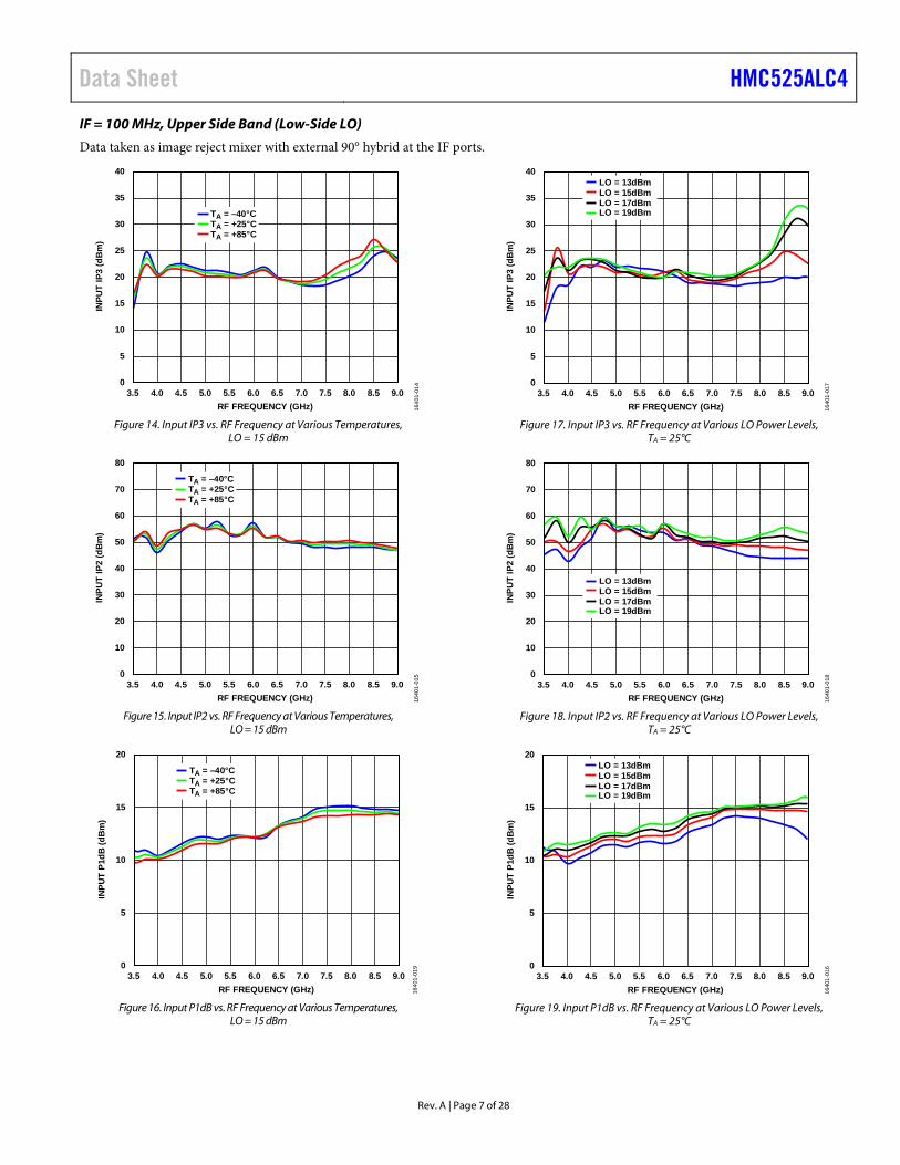
IF = 100 MHz, Upper Side Band (Low-Side LO)
Data taken as image reject mixer with external 90° hybrid at the IF ports.
0
10
20
30
40
5
15
25
35
3.5 4.0 4.5 5.0 5.5 6.0 6.5 7.0 7.5 8.0 8.5 9.0
INPU
T IP
3 (d
Bm
)
RF FREQUENCY (GHz)
TA = –40°CTA = +25°CTA = +85°C
1640
1-01
4
Figure 14. Input IP3 vs. RF Frequency at Various Temperatures, LO = 15 dBm
0
20
40
60
80
10
30
50
70
3.5 4.0 4.5 5.0 5.5 6.0 6.5 7.0 7.5 8.0 8.5 9.0
INPU
T IP
2 (d
Bm
)
RF FREQUENCY (GHz)
TA = –40°CTA = +25°CTA = +85°C
1640
1-01
5
Figure 15. Input IP2 vs. RF Frequency at Various Temperatures,
LO = 15 dBm
0
5
10
15
20
3.5 4.0 4.5 5.0 5.5 6.0 6.5 7.0 7.5 8.0 8.5 9.0
INPU
T P1
dB (d
Bm
)
RF FREQUENCY (GHz) 1640
1-01
9
TA = –40°CTA = +25°CTA = +85°C
Figure 16. Input P1dB vs. RF Frequency at Various Temperatures,
LO = 15 dBm
0
10
20
30
40
5
15
25
35
3.5 4.0 4.5 5.0 5.5 6.0 6.5 7.0 7.5 8.0 8.5 9.0
INPU
T IP
3 (d
Bm
)
RF FREQUENCY (GHz)
LO = 13dBmLO = 15dBmLO = 17dBmLO = 19dBm
1640
1-01
7
Figure 17. Input IP3 vs. RF Frequency at Various LO Power Levels,
TA = 25°C
0
20
40
60
80
10
30
50
70
3.5 4.0 4.5 5.0 5.5 6.0 6.5 7.0 7.5 8.0 8.5 9.0
INPU
T IP
2 (d
Bm
)
RF FREQUENCY (GHz)
LO = 13dBmLO = 15dBmLO = 17dBmLO = 19dBm
1640
1-01
8
Figure 18. Input IP2 vs. RF Frequency at Various LO Power Levels,
TA = 25°C
0
5
10
15
20
3.5 4.0 4.5 5.0 5.5 6.0 6.5 7.0 7.5 8.0 8.5 9.0
INPU
T P1
dB (d
Bm
)
RF FREQUENCY (GHz) 1640
1-01
6
LO = 13dBmLO = 15dBmLO = 17dBmLO = 19dBm
Figure 19. Input P1dB vs. RF Frequency at Various LO Power Levels,
TA = 25°C

HMC525ALC4 Data Sheet
Rev. A | Page 8 of 28
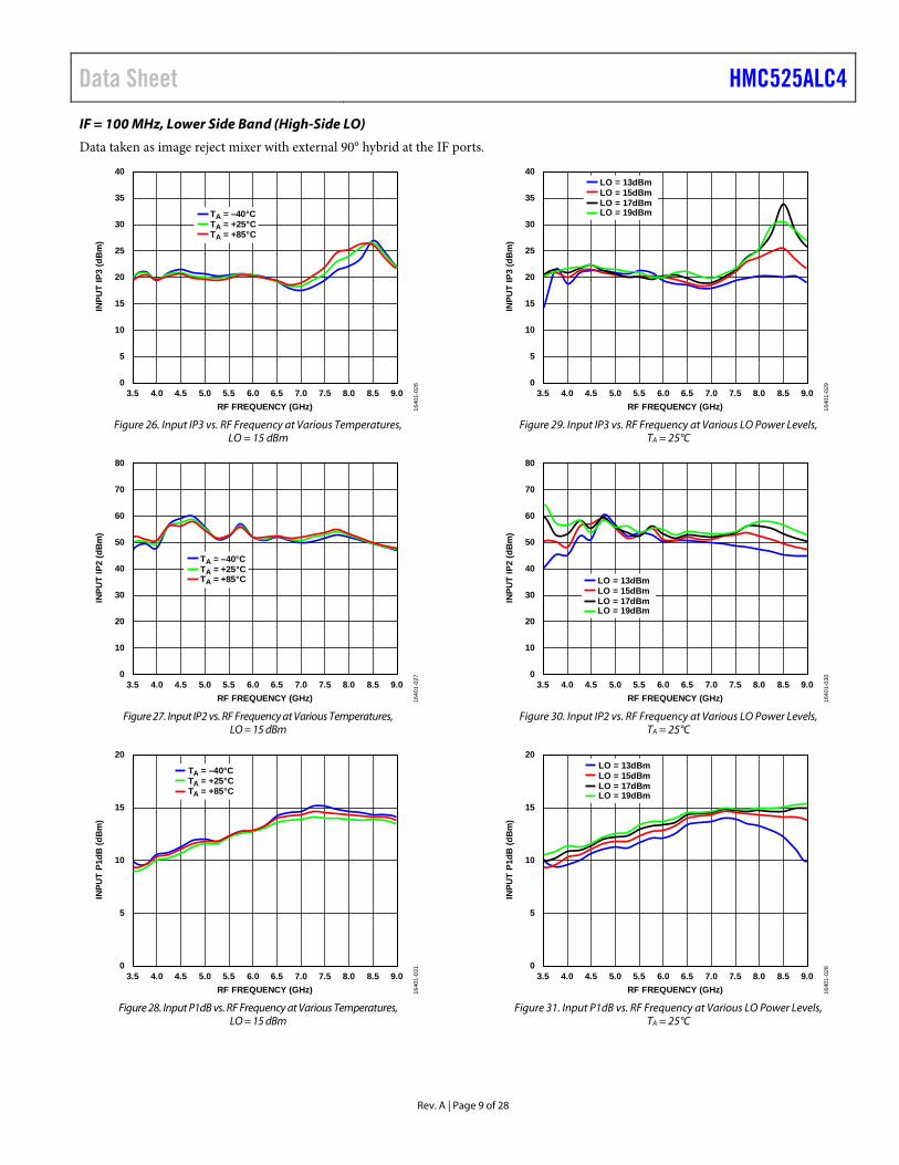
IF = 100 MHz, Lower Side Band (High-Side LO)
Data taken as image reject mixer with external 90° hybrid at the IF ports.
–20
–15
–10
–5
0
3.5 4.0 4.5 5.0 5.5 6.0 6.5 7.0 7.5 8.0 8.5 9.0
CO
NVE
RSI
ON
GA
IN (d
B)
RF FREQUENCY (GHz)
TA = –40°CTA = +25°CTA = +85°C
1640
1-02
0
Figure 20. Conversion Gain vs. RF Frequency at Various Temperatures,
LO = 15 dBm
–40
–30
–20
–10
0
3.5 4.0 4.5 5.0 5.5 6.0 6.5 7.0 7.5 8.0 8.5 9.0
IMA
GE
REJ
ECTI
ON
(dB
c)
RF FREQUENCY (GHz)
TA = –40°CTA = +25°CTA = +85°C
1640
1-02
1
Figure 21. Image Rejection vs. RF Frequency at Various Temperatures,
LO = 15 dBm
0
5
10
15
20
3.5 4.0 4.5 5.0 5.5 6.0 6.5 7.0 7.5 8.0 8.5 9.0
NO
ISE
FIG
UR
E (d
B)
RF FREQUENCY (GHz) 1640
1-02
5
TA = –40°CTA = +25°CTA = +85°C
Figure 22. Noise Figure vs. RF Frequency at Various Temperatures,
LO = 15 dBm
–20
–15
–10
–5
0
3.5 4.0 4.5 5.0 5.5 6.0 6.5 7.0 7.5 8.0 8.5 9.0
CO
NVE
RSI
ON
GA
IN (d
B)
RF FREQUENCY (GHz)
LO = 13dBmLO = 15dBmLO = 17dBmLO = 19dBm
1640
1-02
3
Figure 23. Conversion Gain vs. RF Frequency at Various LO Power Levels,
TA = 25°C
–40
–30
–20
–10
0
3.5 4.0 4.5 5.0 5.5 6.0 6.5 7.0 7.5 8.0 8.5 9.0
IMA
GE
REJ
ECTI
ON
(dB
c)
RF FREQUENCY (GHz)
LO = 13dBmLO = 15dBmLO = 17dBmLO = 19dBm
1640
1-02
4
Figure 24. Image Rejection vs. RF Frequency at Various LO Power Levels,
TA = 25°C
0
5
10
15
20
3.5 4.0 4.5 5.0 5.5 6.0 6.5 7.0 7.5 8.0 8.5 9.0
NO
ISE
FIG
UR
E (d
B)
RF FREQUENCY (GHz) 1640
1-02
2
LO = 13dBmLO = 15dBmLO = 17dBmLO = 19dBm
Figure 25. Noise Figure vs. RF Frequency at Various LO Power Levels,
TA = 25°C
Data Sheet HMC525ALC4
Rev. A | Page 9 of 28
IF = 100 MHz, Lower Side Band (High-Side LO)
Data taken as image reject mixer with external 90° hybrid at the IF ports.
0
10
20
30
40
5
15
25
35
3.5 4.0 4.5 5.0 5.5 6.0 6.5 7.0 7.5 8.0 8.5 9.0
INPU
T IP
3 (d
Bm
)
RF FREQUENCY (GHz)
TA = –40°CTA = +25°CTA = +85°C
1640
1-02
6
Figure 26. Input IP3 vs. RF Frequency at Various Temperatures, LO = 15 dBm
0
20
40
60
80
10
30
50
70
3.5 4.0 4.5 5.0 5.5 6.0 6.5 7.0 7.5 8.0 8.5 9.0
INPU
T IP
2 (d
Bm
)
RF FREQUENCY (GHz)
TA = –40°CTA = +25°CTA = +85°C
1640
1-02
7
Figure 27. Input IP2 vs. RF Frequency at Various Temperatures,
LO = 15 dBm
0
5
10
15
20
3.5 4.0 4.5 5.0 5.5 6.0 6.5 7.0 7.5 8.0 8.5 9.0
INPU
T P1
dB (d
Bm
)
RF FREQUENCY (GHz) 1640
1-03
1
TA = –40°CTA = +25°CTA = +85°C
Figure 28. Input P1dB vs. RF Frequency at Various Temperatures,
LO = 15 dBm
0
10
20
30
40
5
15
25
35
3.5 4.0 4.5 5.0 5.5 6.0 6.5 7.0 7.5 8.0 8.5 9.0
INPU
T IP
3 (d
Bm
)
RF FREQUENCY (GHz)
LO = 13dBmLO = 15dBmLO = 17dBmLO = 19dBm
1640
1-02
9
Figure 29. Input IP3 vs. RF Frequency at Various LO Power Levels,
TA = 25°C
0
20
40
60
80
10
30
50
70
3.5 4.0 4.5 5.0 5.5 6.0 6.5 7.0 7.5 8.0 8.5 9.0
INPU
T IP
2 (d
Bm
)
RF FREQUENCY (GHz)
LO = 13dBmLO = 15dBmLO = 17dBmLO = 19dBm
1640
1-03
0
Figure 30. Input IP2 vs. RF Frequency at Various LO Power Levels,
TA = 25°C
0
5
10
15
20
3.5 4.0 4.5 5.0 5.5 6.0 6.5 7.0 7.5 8.0 8.5 9.0
INPU
T P1
dB (d
Bm
)
RF FREQUENCY (GHz) 1640
1-02
8
LO = 13dBmLO = 15dBmLO = 17dBmLO = 19dBm
Figure 31. Input P1dB vs. RF Frequency at Various LO Power Levels,
TA = 25°C
HMC525ALC4 Data Sheet
Rev. A | Page 10 of 28
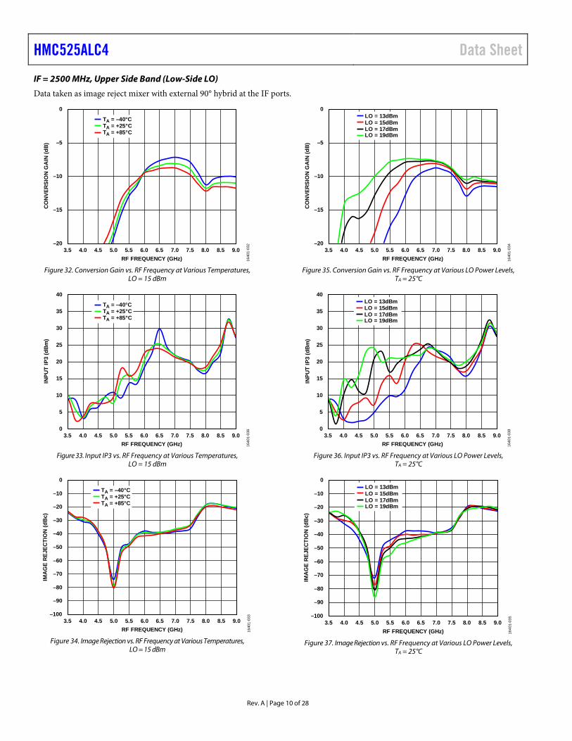
IF = 2500 MHz, Upper Side Band (Low-Side LO)
Data taken as image reject mixer with external 90° hybrid at the IF ports.
–20
–15
–10
–5
0
3.5 4.0 4.5 5.0 5.5 6.0 6.5 7.0 7.5 8.0 8.5 9.0
CO
NVE
RSI
ON
GA
IN (d
B)
RF FREQUENCY (GHz)
TA = –40°CTA = +25°CTA = +85°C
1640
1-03
2
Figure 32. Conversion Gain vs. RF Frequency at Various Temperatures,
LO = 15 dBm
0
10
20
30
40
5
15
25
35
3.5 4.0 4.5 5.0 5.5 6.0 6.5 7.0 7.5 8.0 8.5 9.0
INPU
T IP
3 (d
Bm
)
RF FREQUENCY (GHz)
TA = –40°CTA = +25°CTA = +85°C
1640
1-03
6
Figure 33. Input IP3 vs. RF Frequency at Various Temperatures,
LO = 15 dBm
–100
–90
–70
–50
–30
0
–10
–80
–60
–40
–20
3.5 4.0 4.5 5.0 5.5 6.0 6.5 7.0 7.5 8.0 8.5 9.0
IMA
GE
REJ
ECTI
ON
(dB
c)
RF FREQUENCY (GHz)
TA = –40°CTA = +25°CTA = +85°C
1640
1-03
3
Figure 34. Image Rejection vs. RF Frequency at Various Temperatures,
LO = 15 dBm
–20
–15
–10
–5
0
3.5 4.0 4.5 5.0 5.5 6.0 6.5 7.0 7.5 8.0 8.5 9.0
CO
NVE
RSI
ON
GA
IN (d
B)
RF FREQUENCY (GHz)
LO = 13dBmLO = 15dBmLO = 17dBmLO = 19dBm
1640
1-03
4
Figure 35. Conversion Gain vs. RF Frequency at Various LO Power Levels,
TA = 25°C
0
10
20
30
5
15
25
40
35
3.5 4.0 4.5 5.0 5.5 6.0 6.5 7.0 7.5 8.0 8.5 9.0
INPU
T IP
3 (d
Bm
)
RF FREQUENCY (GHz)
LO = 13dBmLO = 15dBmLO = 17dBmLO = 19dBm
1640
1-03
8
Figure 36. Input IP3 vs. RF Frequency at Various LO Power Levels,
TA = 25°C
–100
–90
–70
–50
–30
0
–10
–80
–60
–40
–20
3.5 4.0 4.5 5.0 5.5 6.0 6.5 7.0 7.5 8.0 8.5 9.0
IMA
GE
REJ
ECTI
ON
(dB
c)
RF FREQUENCY (GHz)
LO = 13dBmLO = 15dBmLO = 17dBmLO = 19dBm
1640
1-03
5
Figure 37. Image Rejection vs. RF Frequency at Various LO Power Levels,
TA = 25°C

Data Sheet HMC525ALC4
Rev. A | Page 11 of 28
IF = 2500 MHz, Lower Side Band (High-Side LO)
Data taken as image-reject mixer with external 90° hybrid at the IF ports.
–20
–15
–10
–5
0
3.5 4.0 4.5 5.0 5.5 6.0 6.5 7.0 7.5 8.0 8.5 9.0
CO
NVE
RSI
ON
GA
IN (d
B)
RF FREQUENCY (GHz)
TA = –40°CTA = +25°CTA = +85°C
1640
1-04
0
Figure 38. Conversion Gain vs. RF Frequency at Various Temperatures, LO = 15 dBm
0
10
20
30
40
5
15
25
35
3.5 4.0 4.5 5.0 5.5 6.0 6.5 7.0 7.5 8.0 8.5 9.0
INPU
T IP
3 (d
Bm
)
RF FREQUENCY (GHz)
TA = –40°CTA = +25°CTA = +85°C
1640
1-04
4
Figure 39. Input IP3 vs. RF Frequency at Various Temperatures, LO = 15 dBm
–60
–50
–40
–30
–20
–10
0
3.5 4.0 4.5 5.0 5.5 6.0 6.5 7.0 7.5 8.0 8.5 9.0
IMA
GE
REJ
ECTI
ON
(dB
c)
RF FREQUENCY (GHz)
TA = –40°CTA = +25°CTA = +85°C
1640
1-04
1
Figure 40. Image Rejection vs. RF Frequency at Various Temperatures,
LO = 15 dBm
–20
–15
–10
–5
0
3.5 4.0 4.5 5.0 5.5 6.0 6.5 7.0 7.5 8.0 8.5 9.0
CO
NVE
RSI
ON
GA
IN (d
B)
RF FREQUENCY (GHz)
LO = 13dBmLO = 15dBmLO = 17dBmLO = 19dBm
1640
1-04
2
Figure 41. Conversion Gain vs. RF Frequency at Various LO Power Levels,
TA = 25°C
0
10
20
35
5
15
25
40
3.5 4.0 4.5 5.0 5.5 6.0 6.5 7.0 7.5 8.0 8.5 9.0
INPU
T IP
3 (d
Bm
)
RF FREQUENCY (GHz)
30
LO = 13dBmLO = 15dBmLO = 17dBmLO = 19dBm
1640
1-04
6
Figure 42. Input IP3 vs. RF Frequency Various LO Power Levels, TA = 25°C
–60
–50
–40
–30
–20
–10
0
3.5 4.0 4.5 5.0 5.5 6.0 6.5 7.0 7.5 8.0 8.5 9.0
IMA
GE
REJ
ECTI
ON
(dB
c)
RF FREQUENCY (GHz) 1640
1-04
3
LO = 13dBmLO = 15dBmLO = 17dBmLO = 19dBm
Figure 43. Image Rejection vs. RF Frequency at Various LO Power Levels,
TA = 25°C
HMC525ALC4 Data Sheet
Rev. A | Page 12 of 28
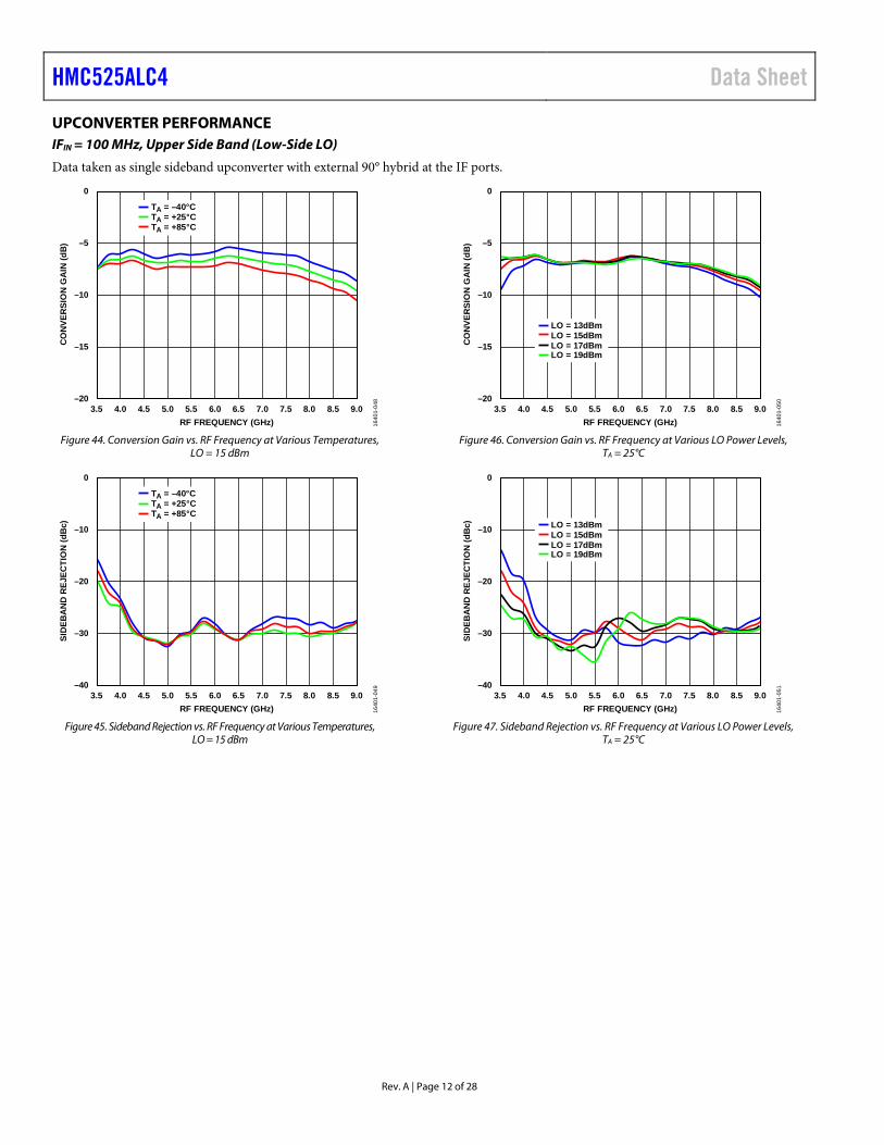
UPCONVERTER PERFORMANCE IFIN = 100 MHz, Upper Side Band (Low-Side LO)
Data taken as single sideband upconverter with external 90° hybrid at the IF ports.
–20
–15
–10
–5
0
3.5 4.0 4.5 5.0 5.5 6.0 6.5 7.0 7.5 8.0 8.5 9.0
CO
NVE
RSI
ON
GA
IN (d
B)
RF FREQUENCY (GHz)
TA = –40°CTA = +25°CTA = +85°C
1640
1-04
8
Figure 44. Conversion Gain vs. RF Frequency at Various Temperatures,
LO = 15 dBm
–40
–30
–20
–10
0
3.5 4.0 4.5 5.0 5.5 6.0 6.5 7.0 7.5 8.0 8.5 9.0
SID
EBA
ND
REJ
ECTI
ON
(dB
c)
RF FREQUENCY (GHz)
TA = –40°CTA = +25°CTA = +85°C
1640
1-04
9
Figure 45. Sideband Rejection vs. RF Frequency at Various Temperatures,
LO = 15 dBm
–20
–15
–10
–5
0
3.5 4.0 4.5 5.0 5.5 6.0 6.5 7.0 7.5 8.0 8.5 9.0
CO
NVE
RSI
ON
GA
IN (d
B)
RF FREQUENCY (GHz)
LO = 13dBmLO = 15dBmLO = 17dBmLO = 19dBm
1640
1-05
0
Figure 46. Conversion Gain vs. RF Frequency at Various LO Power Levels,
TA = 25°C
–40
–30
–20
–10
0
3.5 4.0 4.5 5.0 5.5 6.0 6.5 7.0 7.5 8.0 8.5 9.0
SID
EBA
ND
REJ
ECTI
ON
(dB
c)
RF FREQUENCY (GHz)
LO = 13dBmLO = 15dBmLO = 17dBmLO = 19dBm
1640
1-05
1
Figure 47. Sideband Rejection vs. RF Frequency at Various LO Power Levels,
TA = 25°C

Data Sheet HMC525ALC4
Rev. A | Page 13 of 28
IFIN = 100 MHz, Upper Side Band (Low-Side LO)
Data taken as single sideband upconverter with external 90° hybrid at the IF ports.
0
10
20
30
40
5
15
25
35
3.5 4.0 4.5 5.0 5.5 6.0 6.5 7.0 7.5 8.0 8.5 9.0
INPU
T IP
3 (d
Bm
)
RF FREQUENCY (GHz)
TA = –40°CTA = +25°CTA = +85°C
1640
1-05
2
Figure 48. Input IP3 vs. RF Frequency at Various Temperatures, LO = 15 dBm
0
5
10
15
20
3.5 4.0 4.5 5.0 5.5 6.0 6.5 7.0 7.5 8.0 8.5 9.0
INPU
T P1
dB (d
Bm
)
RF FREQUENCY (GHz) 1640
1-05
5
TA = –40°CTA = +25°CTA = +85°C
Figure 49. Input P1dB vs. RF Frequency at Various Temperatures,
LO = 15 dBm
0
10
20
30
40
5
15
25
35
3.5 4.0 4.5 5.0 5.5 6.0 6.5 7.0 7.5 8.0 8.5 9.0
INPU
T IP
3 (d
Bm
)
RF FREQUENCY (GHz)
LO = 13dBmLO = 15dBmLO = 17dBmLO = 19dBm
1640
1-05
4
Figure 50. Input IP3 vs. RF Frequency at LO Power Levels,
TA = 25°C
0
5
10
15
20
3.5 4.0 4.5 5.0 5.5 6.0 6.5 7.0 7.5 8.0 8.5 9.0
INPU
T P1
dB (d
Bm
)
RF FREQUENCY (GHz) 1640
1-05
3
LO = 13dBmLO = 15dBmLO = 17dBmLO = 19dBm
Figure 51. Input P1dB vs. RF Frequency at Various LO Power Levels,
TA = 25°C

HMC525ALC4 Data Sheet
Rev. A | Page 14 of 28
IFIN = 100 MHz, Lower Side Band (High-Side LO)
Data taken as single sideband upconverter with external 90° hybrid at the IF ports.
–20
–15
–10
–5
0
3.5 4.0 4.5 5.0 5.5 6.0 6.5 7.0 7.5 8.0 8.5 9.0
CO
NVE
RSI
ON
GA
IN (d
B)
RF FREQUENCY (GHz)
TA = –40°CTA = +25°CTA = +85°C
1640
1-05
6
Figure 52. Conversion Gain vs. RF Frequency at Various Temperatures,
LO = 15 dBm
–50
–40
–30
–20
–10
0
3.5 4.0 4.5 5.0 5.5 6.0 6.5 7.0 7.5 8.0 8.5 9.0
SID
EBA
ND
REJ
ECTI
ON
(dB
c)
RF FREQUENCY (GHz)
TA = –40°CTA = +25°CTA = +85°C
1640
1-05
7
Figure 53. Sideband Rejection vs. RF Frequency at Various Temperatures,
LO = 15 dBm
–20
–15
–10
–5
0
3.5 4.0 4.5 5.0 5.5 6.0 6.5 7.0 7.5 8.0 8.5 9.0
CO
NVE
RSI
ON
GA
IN (d
B)
RF FREQUENCY (GHz)
LO = 13dBmLO = 15dBmLO = 17dBmLO = 19dBm
1640
1-05
8
Figure 54. Conversion Gain vs. RF Frequency at Various LO Power Levels,
TA = 25°C
–50
–40
–30
–20
–10
0
3.5 4.0 4.5 5.0 5.5 6.0 6.5 7.0 7.5 8.0 8.5 9.0
SID
EBA
ND
REJ
ECTI
ON
(dB
c)
RF FREQUENCY (GHz)
LO = 13dBmLO = 15dBmLO = 17dBmLO = 19dBm
1640
1-05
9
Figure 55. Sideband Rejection vs. RF Frequency at Various LO Power Levels,
TA = 25°C

Data Sheet HMC525ALC4
Rev. A | Page 15 of 28
IFIN = 100 MHz, Lower Side Band (High-Side LO)
Data taken as single sideband upconverter with external 90° hybrid at the IF ports.
0
10
20
30
40
5
15
25
35
3.5 4.0 4.5 5.0 5.5 6.0 6.5 7.0 7.5 8.0 8.5 9.0
INPU
T IP
3 (d
Bm
)
RF FREQUENCY (GHz)
TA = –40°CTA = +25°CTA = +85°C
1640
1-06
0
Figure 56. Input IP3 vs. RF Frequency at Various Temperatures, LO = 15 dBm
0
5
10
15
20
3.5 4.0 4.5 5.0 5.5 6.0 6.5 7.0 7.5 8.0 8.5 9.0
INPU
T P1
dB (d
Bm
)
RF FREQUENCY (GHz) 1640
1-06
3
TA = –40°CTA = +25°CTA = +85°C
Figure 57. Input P1dB vs. RF Frequency at Various Temperatures,
LO = 15 dBm
0
10
20
5
15
30
40
3.5 4.0 4.5 5.0 5.5 6.0 6.5 7.0 7.5 8.0 8.5 9.0
INPU
T IP
3 (d
Bm
)
RF FREQUENCY (GHz)
25
35
LO = 13dBmLO = 15dBmLO = 17dBmLO = 19dBm
1640
1-06
2
Figure 58. Input IP3 vs. RF Frequency at Various LO Power Levels,
TA = 25°C
0
5
10
15
20
3.5 4.0 4.5 5.0 5.5 6.0 6.5 7.0 7.5 8.0 8.5 9.0
INPU
T P1
dB (d
Bm
)
RF FREQUENCY (GHz) 1640
1-06
1
LO = 13dBmLO = 15dBmLO = 17dBmLO = 19dBm
Figure 59. Input P1dB vs. RF Frequency at Various LO Power Levels,
TA = 25°C

HMC525ALC4 Data Sheet
Rev. A | Page 16 of 28
IFIN = 2500 MHz, Upper Side Band (Low-Side LO)
Data taken as single sideband upconverter with external 90° hybrid at the IF ports.
–20
–15
–10
–5
0
3.5 4.0 4.5 5.0 5.5 6.0 6.5 7.0 7.5 8.0 8.5 9.0
CO
NVE
RSI
ON
GA
IN (d
B)
RF FREQUENCY (GHz)
TA = –40°CTA = +25°CTA = +85°C
1640
1-06
4
Figure 60. Conversion Gain vs. RF Frequency at Various Temperatures,
LO = 15 dBm
0
10
20
30
40
5
15
25
35
3.5 4.0 4.5 5.0 5.5 6.0 6.5 7.0 7.5 8.0 8.5 9.0
INPU
T IP
3 (d
Bm
)
RF FREQUENCY (GHz)
TA = –40°CTA = +25°CTA = +85°C
1640
1-06
8
Figure 61. Input IP3 vs. RF Frequency at Various Temperatures, LO = 15 dBm
–90
–70
–50
–30
0
–10
–80
–60
–40
–20
3.5 4.0 4.5 5.0 5.5 6.0 6.5 7.0 7.5 8.0 8.5 9.0
SID
EBA
ND
REJ
ECTI
ON
(dB
c)
RF FREQUENCY (GHz)
TA = –40°CTA = +25°CTA = +85°C
1640
1-06
5
Figure 62. Sideband Rejection vs. RF Frequency at Various Temperatures,
LO = 15 dBm
–20
–15
–10
–5
0
3.5 4.0 4.5 5.0 5.5 6.0 6.5 7.0 7.5 8.0 8.5 9.0
CO
NVE
RSI
ON
GA
IN (d
B)
RF FREQUENCY (GHz)
LO = 13dBmLO = 15dBmLO = 17dBmLO = 19dBm
1640
1-06
6
Figure 63. Conversion Gain vs. RF Frequency at Various LO Power Levels,
TA = 25°C
0
10
20
5
15
30
40
3.5 4.0 4.5 5.0 5.5 6.0 6.5 7.0 7.5 8.0 8.5 9.0
INPU
T IP
3 (d
Bm
)
RF FREQUENCY (GHz)
25
35 LO = 13dBmLO = 15dBmLO = 17dBmLO = 19dBm
1640
1-07
0
Figure 64. Input IP3 vs. RF Frequency at Various LO Power Levels, TA = 25°C
–90
–70
–50
–30
0
–10
–80
–60
–40
–20
3.5 4.0 4.5 5.0 5.5 6.0 6.5 7.0 7.5 8.0 8.5 9.0
SID
EBA
ND
REJ
ECTI
ON
(dB
c)
RF FREQUENCY (GHz)
LO = 13dBmLO = 15dBmLO = 17dBmLO = 19dBm
1640
1-06
7
Figure 65. Sideband Rejection vs. RF Frequency at Various LO Power Levels,
TA = 25°C
Data Sheet HMC525ALC4
Rev. A | Page 17 of 28
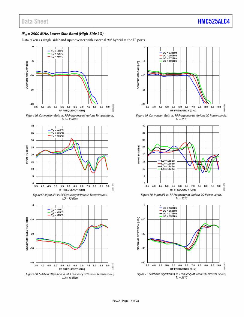
IFIN = 2500 MHz, Lower Side Band (High-Side LO)
Data taken as single sideband upconverter with external 90° hybrid at the IF ports.
–20
–15
–10
–5
0
3.5 4.0 4.5 5.0 5.5 6.0 6.5 7.0 7.5 8.0 8.5 9.0
CO
NVE
RSI
ON
GA
IN (d
B)
RF FREQUENCY (GHz)
TA = –40°CTA = +25°CTA = +85°C
1640
1-07
2
Figure 66. Conversion Gain vs. RF Frequency at Various Temperatures, LO = 15 dBm
0
10
20
30
40
5
15
25
35
3.5 4.0 4.5 5.0 5.5 6.0 6.5 7.0 7.5 8.0 8.5 9.0
INPU
T IP
3 (d
Bm
)
RF FREQUENCY (GHz)
TA = –40°CTA = +25°CTA = +85°C
1640
1-07
6
Figure 67. Input IP3 vs. RF Frequency at Various Temperatures,
LO = 15 dBm
–40
–30
–20
–10
0
3.5 4.0 4.5 5.0 5.5 6.0 6.5 7.0 7.5 8.0 8.5 9.0
SID
EBA
ND
REJ
ECTI
ON
(dB
c)
RF FREQUENCY (GHz)
TA = –40°CTA = +25°CTA = +85°C
1640
1-07
3
Figure 68. Sideband Rejection vs. RF Frequency at Various Temperatures,
LO = 15 dBm
–20
–15
–10
–5
0
3.5 4.0 4.5 5.0 5.5 6.0 6.5 7.0 7.5 8.0 8.5 9.0
CO
NVE
RSI
ON
GA
IN (d
B)
RF FREQUENCY (GHz)
LO = 13dBmLO = 15dBmLO = 17dBmLO = 19dBm
1640
1-07
4
Figure 69. Conversion Gain vs. RF Frequency at Various LO Power Levels,
TA = 25°C
0
10
20
5
15
30
40
3.5 4.0 4.5 5.0 5.5 6.0 6.5 7.0 7.5 8.0 8.5 9.0
INPU
T IP
3 (d
Bm
)
RF FREQUENCY (GHz)
25
35
LO = 13dBmLO = 15dBmLO = 17dBmLO = 19dBm
1640
1-07
8
Figure 70. Input IP3 vs. RF Frequency at Various LO Power Levels,
TA = 25°C
–40
–30
–20
–10
0
3.5 4.0 4.5 5.0 5.5 6.0 6.5 7.0 7.5 8.0 8.5 9.0
SID
EBA
ND
REJ
ECTI
ON
(dB
c)
RF FREQUENCY (GHz) 1640
1-07
5
LO = 13dBmLO = 15dBmLO = 17dBmLO = 19dBm
Figure 71. Sideband Rejection vs. RF Frequency at Various LO Power Levels,
TA = 25°C

HMC525ALC4 Data Sheet
Rev. A | Page 18 of 28
PHASE AND AMPLITUDE BALANCE—DOWNCONVERTER Upper Sideband, IF = 100 MHz
–5
–4
–2
0
2
5
4
–3
–1
1
3
3.5 4.0 4.5 5.0 5.5 6.0 6.5 7.0 7.5 8.0 8.5 9.0
AM
PLIT
UD
E B
ALA
NC
E (d
B)
RF FREQUENCY (GHz)
TA = –40°CTA = +25°CTA = +85°C
1640
1-08
0
Figure 72. Amplitude Balance vs. RF Frequency at Various Temperatures,
LO = 15 dBm
–10
–8
–4
0
4
10
8
–6
–2
2
6
3.5 4.0 4.5 5.0 5.5 6.0 6.5 7.0 7.5 8.0 8.5 9.0
PHA
SE B
ALA
NC
E (D
egre
es)
RF FREQUENCY (GHz)
TA = –40°CTA = +25°CTA = +85°C
1640
1-08
1
Figure 73. Phase Balance vs. RF Frequency at Various Temperatures,
LO = 15 dBm
–5
–4
–2
0
2
5
4
–3
–1
1
3
3.5 4.0 4.5 5.0 5.5 6.0 6.5 7.0 7.5 8.0 8.5 9.0
AM
PLIT
UD
E B
ALA
NC
E (d
B)
RF FREQUENCY (GHz)
LO = 13dBmLO = 15dBmLO = 17dBmLO = 19dBm
1640
1-08
2
Figure 74. Amplitude Balance vs. RF Frequency at Various LO Power Levels,
TA = 25°C
–10
–8
–4
0
4
10
8
–6
–2
2
6
3.5 4.0 4.5 5.0 5.5 6.0 6.5 7.0 7.5 8.0 8.5 9.0
PHA
SE B
ALA
NC
E (D
egre
es)
RF FREQUENCY (GHz)
LO = 13dBmLO = 15dBmLO = 17dBmLO = 19dBm
1640
1-08
3
Figure 75. Phase Balance vs. RF Frequency at Various LO Power Levels,
TA = 25°C

Data Sheet HMC525ALC4
Rev. A | Page 19 of 28
Lower Sideband, IF = 100 MHz
–5
–4
–2
0
2
5
4
–3
–1
1
3
3.5 4.0 4.5 5.0 5.5 6.0 6.5 7.0 7.5 8.0 8.5 9.0
AM
PLIT
UD
E B
ALA
NC
E (d
B)
RF FREQUENCY (GHz)
TA = –40°CTA = +25°CTA = +85°C
1640
1-08
4
Figure 76. Amplitude Balance vs. RF Frequency at Various Temperatures,
LO = 15 dBm
–10
–8
–4
0
4
10
8
–6
–2
2
6
3.5 4.0 4.5 5.0 5.5 6.0 6.5 7.0 7.5 8.0 8.5 9.0
PHA
SE B
ALA
NC
E (D
egre
es)
RF FREQUENCY (GHz)
TA = –40°CTA = +25°CTA = +85°C
1640
1-08
5
Figure 77. Phase Balance vs. RF Frequency at Various Temperatures,
LO = 15 dBm
–5
–4
–2
0
2
5
4
–3
–1
1
3
3.5 4.0 4.5 5.0 5.5 6.0 6.5 7.0 7.5 8.0 8.5 9.0
AM
PLIT
UD
E B
ALA
NC
E (d
B)
RF FREQUENCY (GHz)
LO = 13dBmLO = 15dBmLO = 17dBmLO = 19dBm
1640
1-08
6
Figure 78. Amplitude Balance vs. RF Frequency at Various LO Power Levels,
TA = 25°C
–10
–8
–4
0
4
10
8
–6
–2
2
6
3.5 4.0 4.5 5.0 5.5 6.0 6.5 7.0 7.5 8.0 8.5 9.0
PHA
SE B
ALA
NC
E (D
egre
es)
RF FREQUENCY (GHz)
LO = 13dBmLO = 15dBmLO = 17dBmLO = 19dBm
1640
1-08
7
Figure 79. Phase Balance vs. RF Frequency at Various LO Power Levels,
TA = 25°C

HMC525ALC4 Data Sheet
Rev. A | Page 20 of 28
ISOLATION AND RETURN LOSS Downconverter performance at IF = 100 MHz, upper sideband (low-side LO).
0
10
30
50
70
20
40
60
3.5 4.0 4.5 5.0 5.5 6.0 6.5 7.0 7.5 8.0 8.5 9.0
LO T
O R
F IS
OLA
TIO
N (d
B)
RF FREQUENCY (GHz)
TA = –40°CTA = +25°CTA = +85°C
1640
1-08
8
Figure 80. LO to RF Isolation vs. RF Frequency at Various Temperatures,
LO = 15 dBm
0
10
30
50
70
20
40
60
3.5 4.0 4.5 5.0 5.5 6.0 6.5 7.0 7.5 8.0 8.5 9.0
LO T
O IF
ISO
LATI
ON
(dB
)
RF FREQUENCY (GHz)
LO TO IF1, TA = –40°CLO TO IF1, TA = +25°CLO TO IF1, TA = +85°CLO TO IF2, TA = –40°CLO TO IF2, TA = +25°CLO TO IF2, TA = +85°C
1640
1-08
9
Figure 81. LO to IF Isolation vs. RF Frequency at Various Temperatures,
LO = 15 dBm
0
10
30
50
70
20
40
60
3.5 4.0 4.5 5.0 5.5 6.0 6.5 7.0 7.5 8.0 8.5 9.0
RF
TO IF
ISO
LATI
ON
(dB
)
RF FREQUENCY (GHz)
RF TO IF1, TA = –40°CRF TO IF1, TA = +25°CRF TO IF1, TA = +85°CRF TO IF2, TA = –40°CRF TO IF2, TA = +25°CRF TO IF2, TA = +85°C
1640
1-09
0
Figure 82. RF to IF Isolation vs. RF Frequency at Various Temperatures,
LO = 15 dBm
0
10
30
50
70
20
40
60
3.5 4.0 4.5 5.0 5.5 6.0 6.5 7.0 7.5 8.0 8.5 9.0
LO T
O R
F IS
OLA
TIO
N (d
B)
RF FREQUENCY (GHz)
LO = 13dBmLO = 15dBmLO = 17dBmLO = 19dBm
1640
1-09
1
Figure 83. LO to RF Isolation vs. RF Frequency at Various LO Power levels,
TA = 25°C
0
10
30
50
70
20
40
60
3.5 4.0 4.5 5.0 5.5 6.0 6.5 7.0 7.5 8.0 8.5 9.0
LO T
O IF
ISO
LATI
ON
(dB
)
RF FREQUENCY (GHz)
LO TO IF1, 13dBmLO TO IF1, 15dBmLO TO IF1, 17dBmLO TO IF1, 19dBmLO TO IF2, 13dBmLO TO IF2, 15dBmLO TO IF2, 17dBmLO TO IF1, 19dBm
1640
1-09
2
Figure 84. LO to IF Isolation vs. RF Frequency at Various LO Power Levels,
TA = 25°C
0
10
30
50
70
20
40
60
3.5 4.0 4.5 5.0 5.5 6.0 6.5 7.0 7.5 8.0 8.5 9.0
RF
TO IF
ISO
LATI
ON
(dB
)
RF FREQUENCY (GHz)
RF TO IF1, 13dBmRF TO IF1, 15dBmRF TO IF1, 17dBmRF TO IF1, 19dBmRF TO IF2, 13dBmRF TO IF2, 15dBmRF TO IF2, 17dBmRF TO IF1, 19dBm
1640
1-09
3
Figure 85. RF to IF Isolation vs. RF Frequency at Various LO Power Levels,
TA = 25°C

Data Sheet HMC525ALC4
Rev. A | Page 21 of 28
–40
–30
–20
–10
0
2 3 4 5 6 7 8 9 10
LO R
ETU
RN
LO
SS (d
B)
LO FREQUENCY (GHz) 1640
1-09
4
Figure 86. LO Return Loss vs. LO Frequency at LO = 15 dBm,
TA = 25°C
2 3 4 5 6 7 8 9 10RF FREQUENCY (GHz)
–40
–30
–20
–10
0
RF
RET
UR
N L
OSS
(dB
)
LO = 13dBmLO = 15dBmLO = 17dBmLO = 19dBm
1640
1-09
5
Figure 87. RF Return Loss vs. RF Frequency at Various LO Power Levels,
LO = 5 GHz, TA = 25°C
–60
–50
–40
–30
–20
–10
0
0.1 0.6 1.1 1.6 2.1 2.6 3.1 3.6 4.1 4.6 5.1
IF R
ETU
RN
LO
SS (d
B)
IF FREQUENCY (GHz)
IF1, LO = 13dBmIF1, LO = 15dBmIF1, LO = 17dBmIF1, LO = 19dBmIF2, LO = 13dBmIF2, LO = 15dBmIF2, LO = 17dBmIF2, LO = 19dBm
1640
1-09
6
Figure 88. IF Return Loss vs. IF Frequency at Various LO Power Levels,
LO = 5 GHz, TA = 25°C

HMC525ALC4 Data Sheet
Rev. A | Page 22 of 28
IF BANDWIDTH—DOWNCONVERTER LO = 5 GHz, Upper Side Band
Data taken as image-reject mixer with external 90° hybrid at the IF ports.
0.5 1.0 1.5 2.0 2.5 3.0 3.5 4.0 4.5 5.0IF FREQUENCY (GHz)
–20
–15
–10
–5
0
CO
NVE
RSI
ON
GA
IN (d
B)
TA = –40°CTA = +25°CTA = +85°C
1640
1-09
7
Figure 89. Conversion Gain vs. IF Frequency at Various Temperatures,
LO = 15 dBm
–80
–60
–40
–20
0
–70
–50
–30
–10
0.5 1.0 1.5 2.0 2.5 3.0 3.5 4.0 4.5 5.0
IMA
GE
REJ
ECTI
ON
(dB
c)
IF FREQUENCY (GHz)
TA = –40°CTA = +25°CTA = +85°C
1640
1-09
8
Figure 90. Image Rejection vs. IF Frequency at Various Temperatures,
LO = 15 dBm
0
10
20
30
5
15
25
0.5 1.0 1.5 2.0 2.5 3.0 3.5 4.0 4.5 5.0
INPU
T IP
3 (d
Bm
)
IF FREQUENCY (GHz)
TA = –40°CTA = +25°CTA = +85°C
1640
1-09
9
Figure 91. Input IP3 vs. IF Frequency at Various Temperatures,
LO = 15 dBm
–20
–15
–10
–5
0
CO
NVE
RSI
ON
GA
IN (d
B)
IF FREQUENCY (GHz)0.5 1.0 1.5 2.0 2.5 3.0 3.5 4.0 4.5 5.0
IF FREQUENCY (GHz)
LO = 13dBmLO = 15dBmLO = 17dBmLO = 19dBm
1640
1-10
0
Figure 92. Conversion Gain vs. IF Frequency at Various LO Power Levels,
TA = 25°C
–80
–60
–40
–20
0
–70
–50
–30
–10
0.5 1.0 1.5 2.0 2.5 3.0 3.5 4.0 4.5 5.0
IMA
GE
REJ
ECTI
ON
(dB
c)
IF FREQUENCY (GHz)
LO = 13dBmLO = 15dBmLO = 17dBmLO = 19dBm
1640
1-10
1
Figure 93. Image Rejection vs. IF Frequency at Various LO Power Levels,
TA = 25°C
0
10
20
30
5
15
25
0.5 1.0 1.5 2.0 2.5 3.0 3.5 4.0 4.5 5.0
INPU
T IP
3 (d
Bm
)
IF FREQUENCY (GHz)
LO = 13dBmLO = 15dBmLO = 17dBmLO = 19dBm
1640
1-10
2
Figure 94. Input IP3 vs. IF Frequency at Various LO Power Levels,
TA = 25°C

Data Sheet HMC525ALC4
Rev. A | Page 23 of 28
LO = 8 GHz, Lower Side Band
Data taken as image reject mixer with external 90° hybrid at the IF ports.
–20
–15
–10
–5
0
CO
NVE
RSI
ON
GA
IN (d
B)
IF FREQUENCY (GHz)0.5 1.0 1.5 2.0 2.5 3.0 3.5 4.0 4.5 5.0
IF FREQUENCY (GHz)
TA = –40°CTA = +25°CTA = +85°C
1640
1-10
3
Figure 95. Conversion Gain vs. IF Frequency at Various Temperatures, LO = 15 dBm
–80
–60
–40
–20
0
–70
–50
–30
–10
0.5 1.0 1.5 2.0 2.5 3.0 3.5 4.0 4.5 5.0
IMA
GE
REJ
ECTI
ON
(dB
c)
IF FREQUENCY (GHz)
TA = –40°CTA = +25°CTA = +85°C
1640
1-10
4
Figure 96. Image Rejection vs. IF Frequency at Various Temperatures,
LO = 15 dBm
0
10
20
30
5
15
25
0.5 1.0 1.5 2.0 2.5 3.0 3.5 4.0 4.5 5.0
INPU
T IP
3 (d
Bm
)
IF FREQUENCY (GHz)
TA = –40°CTA = +25°CTA = +85°C
1640
1-10
5
Figure 97. Input IP3 vs. IF Frequency at Various Temperatures,
LO = 15 dBm
–20
–15
–10
–5
0
CO
NVE
RSI
ON
GA
IN (d
B)
IF FREQUENCY (GHz)0.5 1.0 1.5 2.0 2.5 3.0 3.5 4.0 4.5 5.0
IF FREQUENCY (GHz)
LO = 13dBmLO = 15dBmLO = 17dBmLO = 19dBm
1640
1-10
6
Figure 98. Conversion Gain vs. IF Frequency at Various LO Power Levels,
TA = 25°C
–80
–60
–40
–20
0
–70
–50
–30
–10
0.5 1.0 1.5 2.0 2.5 3.0 3.5 4.0 4.5 5.0
IMA
GE
REJ
ECTI
ON
(dB
c)
IF FREQUENCY (GHz)
LO = 13dBmLO = 15dBmLO = 17dBmLO = 19dBm
1640
1-10
7
Figure 99. Image Rejection vs. IF Frequency at Various LO Power Levels,
TA = 25°C
0
10
20
30
5
15
25
0.5 1.0 1.5 2.0 2.5 3.0 3.5 4.0 4.5 5.0
INPU
T IP
3 (d
Bm
)
IF FREQUENCY (GHz)
LO = 13dBmLO = 15dBmLO = 17dBmLO = 19dBm
1640
1-10
8
Figure 100. Input IP3 vs. IF Frequency at Various LO Power Levels,
TA = 25°C
HMC525ALC4 Data Sheet
Rev. A | Page 24 of 28
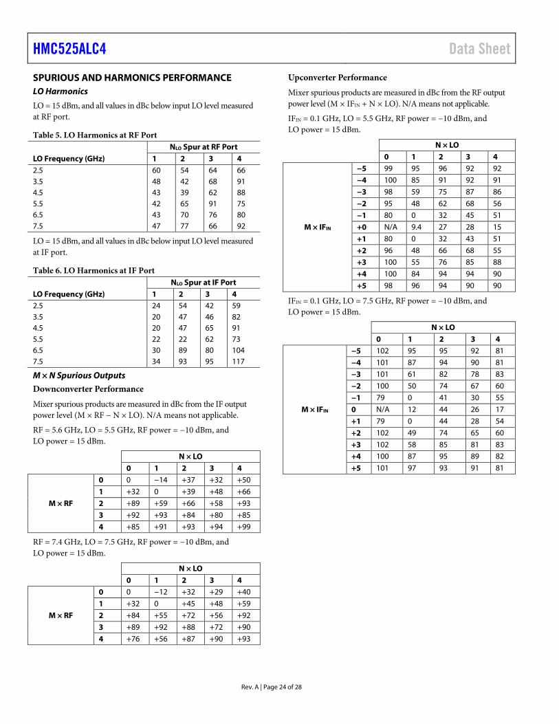
SPURIOUS AND HARMONICS PERFORMANCE LO Harmonics
LO = 15 dBm, and all values in dBc below input LO level measured at RF port.
Table 5. LO Harmonics at RF Port
LO Frequency (GHz) NLO Spur at RF Port
1 2 3 4 2.5 60 54 64 66 3.5 48 42 68 91 4.5 43 39 62 88 5.5 42 65 91 75 6.5 43 70 76 80 7.5 47 77 66 92
LO = 15 dBm, and all values in dBc below input LO level measured at IF port.
Table 6. LO Harmonics at IF Port
LO Frequency (GHz) NLO Spur at IF Port
1 2 3 4 2.5 24 54 42 59 3.5 20 47 46 82 4.5 20 47 65 91 5.5 22 22 62 73 6.5 30 89 80 104 7.5 34 93 95 117
M × N Spurious Outputs
Downconverter Performance
Mixer spurious products are measured in dBc from the IF output power level (M × RF − N × LO). N/A means not applicable.
RF = 5.6 GHz, LO = 5.5 GHz, RF power = −10 dBm, and LO power = 15 dBm.
N × LO 0 1 2 3 4
M × RF
0 0 −14 +37 +32 +50
1 +32 0 +39 +48 +66
2 +89 +59 +66 +58 +93
3 +92 +93 +84 +80 +85
4 +85 +91 +93 +94 +99
RF = 7.4 GHz, LO = 7.5 GHz, RF power = −10 dBm, and LO power = 15 dBm.
N × LO 0 1 2 3 4
M × RF
0 0 −12 +32 +29 +40
1 +32 0 +45 +48 +59
2 +84 +55 +72 +56 +92
3 +89 +92 +88 +72 +90
4 +76 +56 +87 +90 +93
Upconverter Performance
Mixer spurious products are measured in dBc from the RF output power level (M × IFIN + N × LO). N/A means not applicable.
IFIN = 0.1 GHz, LO = 5.5 GHz, RF power = −10 dBm, and LO power = 15 dBm.
N × LO 0 1 2 3 4
M × IFIN
−5 99 95 96 92 92
−4 100 85 91 92 91
−3 98 59 75 87 86
−2 95 48 62 68 56
−1 80 0 32 45 51
+0 N/A 9.4 27 28 15
+1 80 0 32 43 51
+2 96 48 66 68 55
+3 100 55 76 85 88
+4 100 84 94 94 90
+5 98 96 94 90 90
IFIN = 0.1 GHz, LO = 7.5 GHz, RF power = −10 dBm, and LO power = 15 dBm.
N × LO 0 1 2 3 4
M × IFIN
−5 102 95 95 92 81
−4 101 87 94 90 81
−3 101 61 82 78 83
−2 100 50 74 67 60
−1 79 0 41 30 55
0 N/A 12 44 26 17
+1 79 0 44 28 54
+2 102 49 74 65 60
+3 102 58 85 81 83
+4 100 87 95 89 82
+5 101 97 93 91 81

Data Sheet HMC525ALC4
Rev. A | Page 25 of 28
THEORY OF OPERATION The HMC525ALC4 is a compact GaAs, MMIC, I/Q mixer in a 24-terminal, RoHS compliant, ceramic LCC package. The device can be used as either an image reject mixer or a SSB upconverter. The mixer uses two standard double balanced mixer cells and a 90° hybrid fabricated in a GaAs, MESFET
process. This device is a much smaller alternative to a hybrid style image reject mixer and a SSB upconverter assembly. The HMC525ALC4 eliminates the need for wire bonding, allowing the use of the surface-mount manufacturing techniques.
HMC525ALC4 Data Sheet
Rev. A | Page 26 of 28
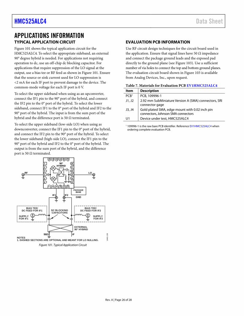
APPLICATIONS INFORMATION TYPICAL APPLICATION CIRCUIT Figure 101 shows the typical application circuit for the HMC525ALC4. To select the appropriate sideband, an external 90° degree hybrid is needed. For applications not requiring operation to dc, use an off-chip dc blocking capacitor. For applications that require suppression of the LO signal at the output, use a bias tee or RF feed as shown in Figure 101. Ensure that the source or sink current used for LO suppression is <2 mA for each IF port to prevent damage to the device. The common-mode voltage for each IF port is 0 V.
To select the upper sideband when using as an upconverter, connect the IF1 pin to the 90° port of the hybrid, and connect the IF2 pin to the 0° port of the hybrid. To select the lower sideband, connect IF1 to the 0° port of the hybrid and IF2 to the 90° port of the hybrid. The input is from the sum port of the hybrid and the difference port is 50 Ω terminated.
To select the upper sideband (low-side LO) when using as downconverter, connect the IF1 pin to the 0° port of the hybrid, and connect the IF2 pin to the 90° port of the hybrid. To select the lower sideband (high-side LO), connect the IF1 pin to the 90° port of the hybrid and IF2 to the 0° port of the hybrid. The output is from the sum port of the hybrid, and the difference port is 50 Ω terminated.
13
1
3
4
2
7
5
6
14
15
16
17
1890°HYBRID
RF LO
8 9 10 11 1219
GNDIF1 IF2
2021222324
PACKAGEBASE
1640
1-10
950Ω IF
SUPPLYFOR IF1
SUPPLYFOR IF2
BIAS TEE/DC FEED FOR IF2
BIAS TEE/DC FEED FOR IF1 DC BLOCKING
CAPACITORS
EXTERNAL90° HYBRID
NOTES1. DASHED SECTIONS ARE OPTIONAL AND MEANT FOR LO NULLING.
Figure 101. Typical Application Circuit
EVALUATION PCB INFORMATION Use RF circuit design techniques for the circuit board used in the application. Ensure that signal lines have 50 Ω impedance and connect the package ground leads and the exposed pad directly to the ground plane (see Figure 103). Use a sufficient number of via holes to connect the top and bottom ground planes. The evaluation circuit board shown in Figure 103 is available from Analog Devices, Inc., upon request.
Table 7. Materials for Evaluation PCB EV1HMC525ALC4 Item Description PCB1 PCB, 109996-1 J1, J2 2.92 mm SubMiniature Version A (SMA) connectors, SRI
connector gage J3, J4 Gold plated SMA, edge mount with 0.02 inch pin
connectors, Johnson SMA connectors U1 Device under test, HMC525ALC4
1 109996-1 is the raw bare PCB identifier. Reference EV1HMC525ALC4 when ordering complete evaluation PCB.

Data Sheet HMC525ALC4
Rev. A | Page 27 of 28
SOLDERING INFORMATION AND RECOMMENDED LAND PATTERN Figure 102 shows the recommended land pattern for the HMC525ALC4. The HMC525ALC4 is contained in a 4 mm × 4 mm, 24-terminal, ceramic LCC package, with an exposed ground pad (EPAD). This pad is internally connected to the ground of the chip. To minimize thermal impedance and ensure
electrical performance, solder the pad to the low impedance ground plane on the PCB. It is recommended that the ground planes on all layers under the pad be stitched together with vias, to further reduce thermal impedance. The land pattern on the EV1HMC525ALC4 evaluation board provides a simulated thermal resistance (θJC) of 161°C/W.
.010" REF.030"
MASK OPENING .098" SQUARE MASK OPENING.020 × 45" CHAMFER FOR PIN 1
.106" SQUAREGROUND PAD
.116"MASK
OPENING
PIN 1.0197"[0.50]
.034"TYPICAL
VIASPACING
PAD SIZE.026" × .010"
ᶲ .010"TYPICAL VIA
GROUND PAD
SOLDERMASK.004" MASK/METAL OVERLAP
.178" SQUARE
.010" MIN MASK WIDTH
1640
1-11
1
Figure 102. Evaluation Board Land Pattern for the HMC525ALC4 Package
1164
01-1
10
Figure 103. Evaluation PCB Top Layer

HMC525ALC4 Data Sheet
Rev. A | Page 28 of 28
OUTLINE DIMENSIONS
12
0.50BSC
2.50 REFBOTTOM VIEWTOP VIEW
124
7
13
1819
6
02-2
7-20
17-B
0.360.300.24
EXPOSEDPAD
PKG
-004
840
PIN 1INDICATOR
4.053.90 SQ3.75
3.10 BSC
FOR PROPER CONNECTION OFTHE EXPOSED PAD, REFER TOTHE PIN CONFIGURATION ANDFUNCTION DESCRIPTIONSSECTION OF THIS DATA SHEET.
2.602.50 SQ2.40
PIN 1
0.32BSC
0.08BSC
SIDE VIEW1.000.900.80
SEATINGPLANE
Figure 104. 24-Terminal Ceramic Leadless Chip Carrier [LCC]
(E-24-1) Dimensions shown in millimeters
ORDERING GUIDE Model1 Temperature Range Package Description Package Option HMC525ALC4 −40°C to +85°C 24-Terminal Ceramic LCC E-24-1 HMC525ALC4TR −40°C to +85°C 24-Terminal Ceramic LCC E-24-1 HMC525ALC4TR-R5 −40°C to +85°C 24-Terminal Ceramic LCC E-24-1 EV1HMC525ALC4 Evaluation PCB Assembly
1 The HMC525ALC4, HMC525ALC4TR, and HMC525ALC4TR-R5 are RoHS compliant.
©2018 Analog Devices, Inc. All rights reserved. Trademarks and registered trademarks are the property of their respective owners. D16401-0-5/18(A)
Related Documents