Rethinking Memory System Design for Data-Intensive Computing Onur Mutlu [email protected] December 6, 2013 IAP Cloud Workshop

Welcome message from author
This document is posted to help you gain knowledge. Please leave a comment to let me know what you think about it! Share it to your friends and learn new things together.
Transcript

Rethinking Memory System Design for
Data-Intensive Computing
Onur Mutlu
December 6, 2013
IAP Cloud Workshop

The Main Memory/Storage System
Main memory is a critical component of all computing systems: server, mobile, embedded, desktop, sensor
Main memory system must scale (in size, technology, efficiency, cost, and management algorithms) to maintain performance growth and technology scaling benefits
2
Processor
and caches Main Memory Storage (SSD/HDD)

Memory System: A Shared Resource View
3
Storage

State of the Main Memory System
Recent technology, architecture, and application trends
lead to new requirements
exacerbate old requirements
DRAM and memory controllers, as we know them today, are (will be) unlikely to satisfy all requirements
Some emerging non-volatile memory technologies (e.g., PCM) enable new opportunities: memory+storage merging
We need to rethink the main memory system
to fix DRAM issues and enable emerging technologies
to satisfy all requirements
4

Agenda
Major Trends Affecting Main Memory
The Memory Scaling Problem and Solution Directions
New Memory Architectures
Enabling Emerging Technologies: Hybrid Memory Systems
How Can We Do Better?
Summary
5

Major Trends Affecting Main Memory (I)
Need for main memory capacity, bandwidth, QoS increasing
Main memory energy/power is a key system design concern
DRAM technology scaling is ending
6

Major Trends Affecting Main Memory (II)
Need for main memory capacity, bandwidth, QoS increasing
Multi-core: increasing number of cores/agents
Data-intensive applications: increasing demand/hunger for data
Consolidation: cloud computing, GPUs, mobile, heterogeneity
Main memory energy/power is a key system design concern
DRAM technology scaling is ending
7

Example: The Memory Capacity Gap
Memory capacity per core expected to drop by 30% every two years
Trends worse for memory bandwidth per core! 8
Core count doubling ~ every 2 years
DRAM DIMM capacity doubling ~ every 3 years
Major Trends Affecting Main Memory (III)
Need for main memory capacity, bandwidth, QoS increasing
Main memory energy/power is a key system design concern
~40-50% energy spent in off-chip memory hierarchy [Lefurgy,
IEEE Computer 2003]
DRAM consumes power even when not used (periodic refresh)
DRAM technology scaling is ending
9

Major Trends Affecting Main Memory (IV)
Need for main memory capacity, bandwidth, QoS increasing
Main memory energy/power is a key system design concern
DRAM technology scaling is ending
ITRS projects DRAM will not scale easily below X nm
Scaling has provided many benefits:
higher capacity (density), lower cost, lower energy
10

Agenda
Major Trends Affecting Main Memory
The Memory Scaling Problem and Solution Directions
New Memory Architectures
Enabling Emerging Technologies: Hybrid Memory Systems
How Can We Do Better?
Summary
11
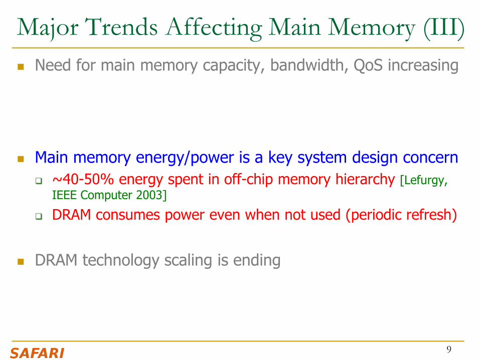
The DRAM Scaling Problem
DRAM stores charge in a capacitor (charge-based memory)
Capacitor must be large enough for reliable sensing
Access transistor should be large enough for low leakage and high retention time
Scaling beyond 40-35nm (2013) is challenging [ITRS, 2009]
DRAM capacity, cost, and energy/power hard to scale
12

Solutions to the DRAM Scaling Problem
Two potential solutions
Tolerate DRAM (by taking a fresh look at it)
Enable emerging memory technologies to eliminate/minimize DRAM
Do both
Hybrid memory systems
13

Solution 1: Tolerate DRAM Overcome DRAM shortcomings with
System-DRAM co-design
Novel DRAM architectures, interface, functions
Better waste management (efficient utilization)
Key issues to tackle
Reduce energy
Enable reliability at low cost
Improve bandwidth and latency
Reduce waste
Liu, Jaiyen, Veras, Mutlu, “RAIDR: Retention-Aware Intelligent DRAM Refresh,” ISCA 2012.
Kim, Seshadri, Lee+, “A Case for Exploiting Subarray-Level Parallelism in DRAM,” ISCA 2012.
Lee+, “Tiered-Latency DRAM: A Low Latency and Low Cost DRAM Architecture,” HPCA 2013.
Liu+, “An Experimental Study of Data Retention Behavior in Modern DRAM Devices,” ISCA 2013.
Seshadri+, “RowClone: Fast and Efficient In-DRAM Copy and Initialization of Bulk Data,” MICRO 2013.
Pekhimenko+, “Linearly Compressed Pages: A Main Memory Compression Framework,” MICRO 2013.
14

Solution 2: Emerging Memory Technologies Some emerging resistive memory technologies seem more
scalable than DRAM (and they are non-volatile)
Example: Phase Change Memory
Expected to scale to 9nm (2022 [ITRS])
Expected to be denser than DRAM: can store multiple bits/cell
But, emerging technologies have shortcomings as well
Can they be enabled to replace/augment/surpass DRAM?
Lee, Ipek, Mutlu, Burger, “Architecting Phase Change Memory as a Scalable DRAM Alternative,” ISCA 2009, CACM 2010, Top Picks 2010.
Meza, Chang, Yoon, Mutlu, Ranganathan, “Enabling Efficient and Scalable Hybrid Memories,” IEEE Comp. Arch. Letters 2012.
Yoon, Meza et al., “Row Buffer Locality Aware Caching Policies for Hybrid Memories,” ICCD 2012.
Kultursay+, “Evaluating STT-RAM as an Energy-Efficient Main Memory Alternative,” ISPASS 2013.
Meza+, “A Case for Efficient Hardware-Software Cooperative Management of Storage and Memory,” WEED 2013.
15

Hybrid Memory Systems
Meza+, “Enabling Efficient and Scalable Hybrid Memories,” IEEE Comp. Arch. Letters, 2012.
Yoon, Meza et al., “Row Buffer Locality Aware Caching Policies for Hybrid Memories,” ICCD 2012 Best Paper Award.
CPU DRAMCtrl
Fast, durable Small,
leaky, volatile, high-cost
Large, non-volatile, low-cost Slow, wears out, high active energy
PCM Ctrl DRAM Phase Change Memory (or Tech. X)
Hardware/software manage data allocation and movement to achieve the best of multiple technologies

An Orthogonal Issue: Memory Interference
Main Memory
17
Core Core
Core Core
Cores’ interfere with each other when accessing shared main memory

Problem: Memory interference between cores is uncontrolled
unfairness, starvation, low performance
uncontrollable, unpredictable, vulnerable system
Solution: QoS-Aware Memory Systems
Hardware designed to provide a configurable fairness substrate
Application-aware memory scheduling, partitioning, throttling
Software designed to configure the resources to satisfy different QoS goals
QoS-aware memory controllers and interconnects can provide predictable performance and higher efficiency
An Orthogonal Issue: Memory Interference

Designing QoS-Aware Memory Systems: Approaches
Smart resources: Design each shared resource to have a configurable interference control/reduction mechanism
QoS-aware memory controllers [Mutlu+ MICRO’07] [Moscibroda+, Usenix Security’07]
[Mutlu+ ISCA’08, Top Picks’09] [Kim+ HPCA’10] [Kim+ MICRO’10, Top Picks’11] [Ebrahimi+ ISCA’11, MICRO’11] [Ausavarungnirun+, ISCA’12][Subramanian+, HPCA’13]
QoS-aware interconnects [Das+ MICRO’09, ISCA’10, Top Picks ’11] [Grot+ MICRO’09,
ISCA’11, Top Picks ’12]
QoS-aware caches
Dumb resources: Keep each resource free-for-all, but reduce/control interference by injection control or data mapping
Source throttling to control access to memory system [Ebrahimi+ ASPLOS’10,
ISCA’11, TOCS’12] [Ebrahimi+ MICRO’09] [Nychis+ HotNets’10] [Nychis+ SIGCOMM’12]
QoS-aware data mapping to memory controllers [Muralidhara+ MICRO’11]
QoS-aware thread scheduling to cores [Das+ HPCA’13]
19

Some Current Directions
New memory/storage + compute architectures Rethinking DRAM
Processing close to data; accelerating bulk operations
Ensuring memory/storage reliability and robustness
Enabling emerging NVM technologies Hybrid memory systems with automatic data management
Coordinated management of memory and storage with NVM
System-level memory/storage QoS QoS-aware controller and system design
Coordinated memory + storage QoS
20

Agenda
Major Trends Affecting Main Memory
The Memory Scaling Problem and Solution Directions
New Memory Architectures
Enabling Emerging Technologies: Hybrid Memory Systems
How Can We Do Better?
Summary
21

Tolerating DRAM: Example Techniques
Retention-Aware DRAM Refresh: Reducing Refresh Impact
Tiered-Latency DRAM: Reducing DRAM Latency
RowClone: Accelerating Page Copy and Initialization
Subarray-Level Parallelism: Reducing Bank Conflict Impact
Linearly Compressed Pages: Efficient Memory Compression
22

DRAM Refresh
DRAM capacitor charge leaks over time
The memory controller needs to refresh each row periodically to restore charge
Activate each row every N ms
Typical N = 64 ms
Downsides of refresh
-- Energy consumption: Each refresh consumes energy
-- Performance degradation: DRAM rank/bank unavailable while refreshed
-- QoS/predictability impact: (Long) pause times during refresh
-- Refresh rate limits DRAM capacity scaling
23

Refresh Overhead: Performance
24
8%
46%

Refresh Overhead: Energy
25
15%
47%

Retention Time Profile of DRAM
26

RAIDR: Eliminating Unnecessary Refreshes
Observation: Most DRAM rows can be refreshed much less often without losing data [Kim+, EDL’09][Liu+ ISCA’13]
Key idea: Refresh rows containing weak cells
more frequently, other rows less frequently
1. Profiling: Profile retention time of all rows
2. Binning: Store rows into bins by retention time in memory controller
Efficient storage with Bloom Filters (only 1.25KB for 32GB memory)
3. Refreshing: Memory controller refreshes rows in different bins at different rates
Results: 8-core, 32GB, SPEC, TPC-C, TPC-H
74.6% refresh reduction @ 1.25KB storage
~16%/20% DRAM dynamic/idle power reduction
~9% performance improvement
Benefits increase with DRAM capacity
27 Liu et al., “RAIDR: Retention-Aware Intelligent DRAM Refresh,” ISCA 2012.

Going Forward
How to find out and expose weak memory cells/rows
Analysis of modern DRAM chips:
Liu+, “An Experimental Study of Data Retention Behavior in Modern DRAM Devices: Implications for Retention Time Profiling Mechanisms”, ISCA 2013.
Low-cost system-level tolerance of memory errors
Tolerating cell-to-cell interference at the system level
For both DRAM and Flash. Analysis of Flash chips:
Cai+, “Program Interference in MLC NAND Flash Memory: Characterization, Modeling, and Mitigation,” ICCD 2013.
28

Tolerating DRAM: Example Techniques
Retention-Aware DRAM Refresh: Reducing Refresh Impact
Tiered-Latency DRAM: Reducing DRAM Latency
RowClone: Accelerating Page Copy and Initialization
Subarray-Level Parallelism: Reducing Bank Conflict Impact
Linearly Compressed Pages: Efficient Memory Compression
29

30
DRAM Latency-Capacity Trend
0
20
40
60
80
100
0.0
0.5
1.0
1.5
2.0
2.5
2000 2003 2006 2008 2011
Late
ncy
(n
s)
Cap
acit
y (G
b)
Year
Capacity Latency (tRC)
16X
-20%
DRAM latency continues to be a critical bottleneck

31
DRAM Latency = Subarray Latency + I/O Latency
What Causes the Long Latency? DRAM Chip
channel
cell array
I/O
DRAM Chip
channel
I/O
subarray
DRAM Latency = Subarray Latency + I/O Latency
Dominant Su
bar
ray
I/O

32
Why is the Subarray So Slow?
Subarray
row
dec
od
er
sense amplifier
cap
acit
or
access transistor
wordline
bit
line
Cell
large sense amplifier
bit
line:
51
2 c
ells
cell
• Long bitline – Amortizes sense amplifier cost Small area
– Large bitline capacitance High latency & power
sen
se a
mp
lifie
r
row
dec
od
er

33
Trade-Off: Area (Die Size) vs. Latency
Faster
Smaller
Short Bitline
Long Bitline
Trade-Off: Area vs. Latency

34
Trade-Off: Area (Die Size) vs. Latency
0
1
2
3
4
0 10 20 30 40 50 60 70
No
rmal
ize
d D
RA
M A
rea
Latency (ns)
64
32
128
256 512 cells/bitline
Commodity DRAM
Long Bitline
Ch
eap
er
Faster
Fancy DRAM Short Bitline

35
Short Bitline
Low Latency
Approximating the Best of Both Worlds
Long Bitline
Small Area
Long Bitline
Low Latency
Short Bitline Our Proposal
Small Area
Short Bitline Fast
Need Isolation
Add Isolation Transistors
High Latency
Large Area

36
Approximating the Best of Both Worlds
Low Latency
Our Proposal
Small Area Long Bitline Small Area
Long Bitline
High Latency
Short Bitline
Low Latency
Short Bitline
Large Area
Tiered-Latency DRAM
Low Latency
Small area using long
bitline

37
Tiered-Latency DRAM
Near Segment
Far Segment
Isolation Transistor
• Divide a bitline into two segments with an isolation transistor
Sense Amplifier
Lee+, “Tiered-Latency DRAM: A Low Latency and Low Cost DRAM Architecture,” HPCA 2013.

38
0%
50%
100%
150%
0%
50%
100%
150%
Commodity DRAM vs. TL-DRAM La
ten
cy
Po
we
r
–56%
+23%
–51%
+49%
• DRAM Latency (tRC) • DRAM Power
• DRAM Area Overhead ~3%: mainly due to the isolation transistors
TL-DRAM Commodity
DRAM
Near Far Commodity
DRAM
Near Far
TL-DRAM
(52.5ns)

39
Trade-Off: Area (Die-Area) vs. Latency
0
1
2
3
4
0 10 20 30 40 50 60 70
No
rmal
ize
d D
RA
M A
rea
Latency (ns)
64
32
128 256 512 cells/bitline
Ch
eap
er
Faster
Near Segment Far Segment

40
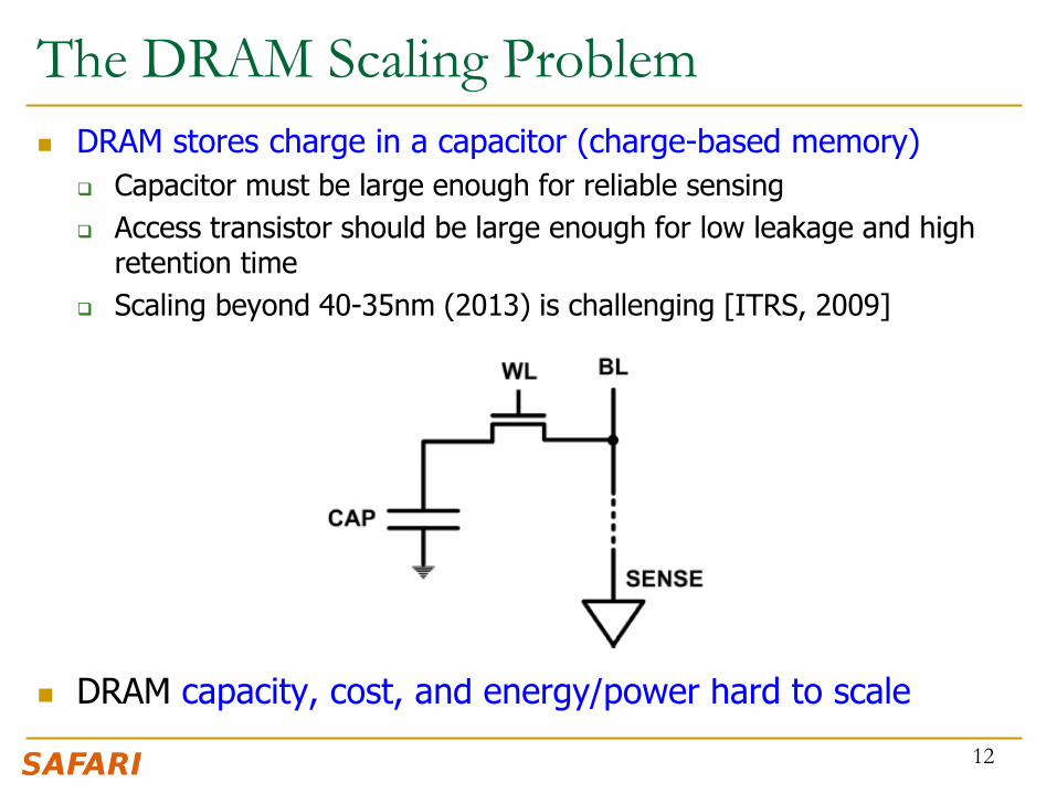
Leveraging Tiered-Latency DRAM
• TL-DRAM is a substrate that can be leveraged by the hardware and/or software
• Many potential uses 1. Use near segment as hardware-managed inclusive
cache to far segment
2. Use near segment as hardware-managed exclusive cache to far segment
3. Profile-based page mapping by operating system
4. Simply replace DRAM with TL-DRAM
41
0%
20%
40%
60%
80%
100%
120%
1 (1-ch) 2 (2-ch) 4 (4-ch)0%
20%
40%
60%
80%
100%
120%
1 (1-ch) 2 (2-ch) 4 (4-ch)
Performance & Power Consumption
11.5%
No
rmal
ize
d P
erf
orm
ance
Core-Count (Channel) N
orm
aliz
ed
Po
we
r Core-Count (Channel)
10.7%
12.4% –23%
–24%
–26%
Using near segment as a cache improves performance and reduces power consumption

Tolerating DRAM: Example Techniques
Retention-Aware DRAM Refresh: Reducing Refresh Impact
Tiered-Latency DRAM: Reducing DRAM Latency
RowClone: Accelerating Page Copy and Initialization
Subarray-Level Parallelism: Reducing Bank Conflict Impact
Linearly Compressed Pages: Efficient Memory Compression
42

Today’s Memory: Bulk Data Copy
Memory
MC L3 L2 L1 CPU
1) High latency
2) High bandwidth utilization
3) Cache pollution
4) Unwanted data movement
43 1046ns, 3.6uJ

Future: RowClone (In-Memory Copy)
Memory
MC L3 L2 L1 CPU
1) Low latency
2) Low bandwidth utilization
3) No cache pollution
4) No unwanted data movement
44 1046ns, 3.6uJ 90ns, 0.04uJ
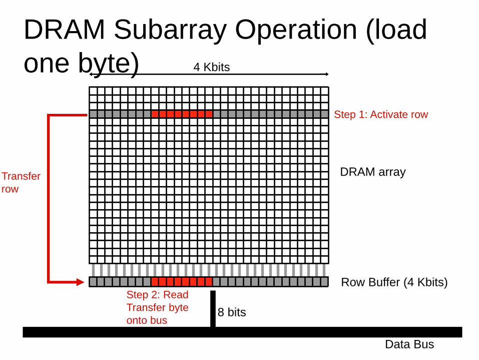
DRAM Subarray Operation (load
one byte)
Row Buffer (4 Kbits)
Data Bus
8 bits
DRAM array
4 Kbits
Step 1: Activate row
Transfer
row
Step 2: Read
Transfer byte
onto bus

RowClone: In-DRAM Row Copy
(and Initialization)
Row Buffer (4 Kbits)
Data Bus
8 bits
DRAM array
4 Kbits
Step 1: Activate row A
Transfer
row
Step 2: Activate row B
Transfer
row 0.01% area cost

RowClone: Latency and Energy Savings
0
0.2
0.4
0.6
0.8
1
1.2
Latency Energy
No
rmal
ize
d S
avin
gs
Baseline Intra-Subarray
Inter-Bank Inter-Subarray
11.6x 74x
47 Seshadri et al., “RowClone: Fast and Efficient In-DRAM Copy and Initialization of Bulk Data,” MICRO 2013.

RowClone: Overall Performance
48
0
10
20
30
40
50
60
70
80
bootup compile forkbench mcached mysql shell
% C
om
pare
d t
o B
aseli
ne
IPC Improvement Energy Reduction
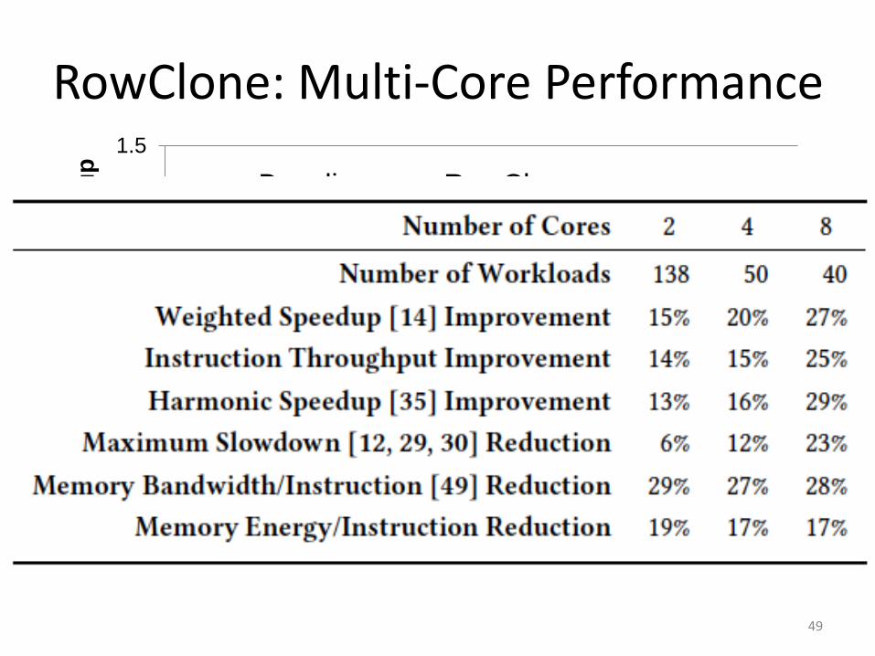
RowClone: Multi-Core Performance
49
0.9
1
1.1
1.2
1.3
1.4
1.5
No
rma
lize
d W
eig
hte
d S
pe
ed
up
50 Workloads (4-core)
Baseline RowClone

Goal: Ultra-Efficient Processing
Close to Data CPU core
CPU core
CPU core
CPU core
mini-CPU core
video core
GPU (throughput)
core
GPU (throughput)
core
GPU (throughput)
core
GPU (throughput)
core
LLC
Memory Controller
Specialized compute-capability
in memory
Memory imaging core
Memory Bus
Slide credit: Prof. Kayvon Fatahalian, CMU

Enabling Ultra-Efficient (Visual)
Search
▪ What is the right partitioning of computation
capability?
▪ What is the right low-cost memory substrate?
▪ What memory technologies are the best
enablers?
▪ How do we rethink/ease (visual) search
algorithms/applications?
Cache
Processor Core
Interconnect
Memory
Database (of images)
Query vector
Results
Picture credit: Prof. Kayvon Fatahalian, CMU

Tolerating DRAM: Example Techniques
Retention-Aware DRAM Refresh: Reducing Refresh Impact
Tiered-Latency DRAM: Reducing DRAM Latency
RowClone: Accelerating Page Copy and Initialization
Subarray-Level Parallelism: Reducing Bank Conflict Impact
Linearly Compressed Pages: Efficient Memory Compression
52

Agenda
Major Trends Affecting Main Memory
The Memory Scaling Problem and Solution Directions
New Memory Architectures
Enabling Emerging Technologies: Hybrid Memory Systems
How Can We Do Better?
Summary
53

Solution 2: Emerging Memory Technologies
Some emerging resistive memory technologies seem more scalable than DRAM (and they are non-volatile)
Example: Phase Change Memory
Data stored by changing phase of material
Data read by detecting material’s resistance
Expected to scale to 9nm (2022 [ITRS])
Prototyped at 20nm (Raoux+, IBM JRD 2008)
Expected to be denser than DRAM: can store multiple bits/cell
But, emerging technologies have (many) shortcomings
Can they be enabled to replace/augment/surpass DRAM?
54
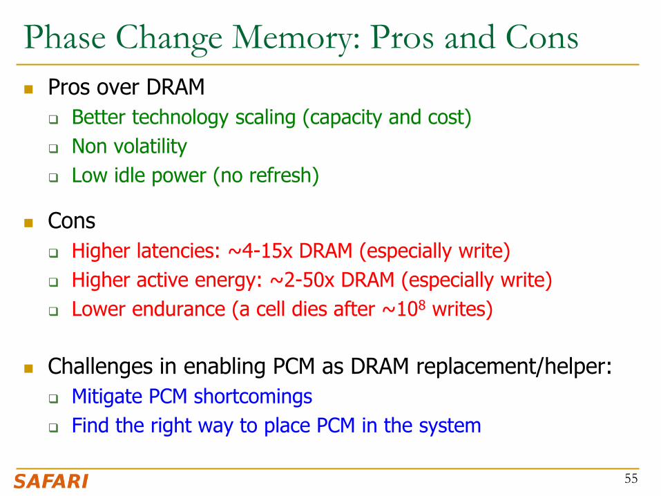
Phase Change Memory: Pros and Cons
Pros over DRAM
Better technology scaling (capacity and cost)
Non volatility
Low idle power (no refresh)
Cons
Higher latencies: ~4-15x DRAM (especially write)
Higher active energy: ~2-50x DRAM (especially write)
Lower endurance (a cell dies after ~108 writes)
Challenges in enabling PCM as DRAM replacement/helper:
Mitigate PCM shortcomings
Find the right way to place PCM in the system
55

PCM-based Main Memory (I)
How should PCM-based (main) memory be organized?
Hybrid PCM+DRAM [Qureshi+ ISCA’09, Dhiman+ DAC’09]:
How to partition/migrate data between PCM and DRAM
56

PCM-based Main Memory (II)
How should PCM-based (main) memory be organized?
Pure PCM main memory [Lee et al., ISCA’09, Top Picks’10]:
How to redesign entire hierarchy (and cores) to overcome PCM shortcomings
57

An Initial Study: Replace DRAM with PCM
Lee, Ipek, Mutlu, Burger, “Architecting Phase Change Memory as a Scalable DRAM Alternative,” ISCA 2009.
Surveyed prototypes from 2003-2008 (e.g. IEDM, VLSI, ISSCC)
Derived “average” PCM parameters for F=90nm
58

Results: Naïve Replacement of DRAM with PCM
Replace DRAM with PCM in a 4-core, 4MB L2 system
PCM organized the same as DRAM: row buffers, banks, peripherals
1.6x delay, 2.2x energy, 500-hour average lifetime
Lee, Ipek, Mutlu, Burger, “Architecting Phase Change Memory as a Scalable DRAM Alternative,” ISCA 2009.
59
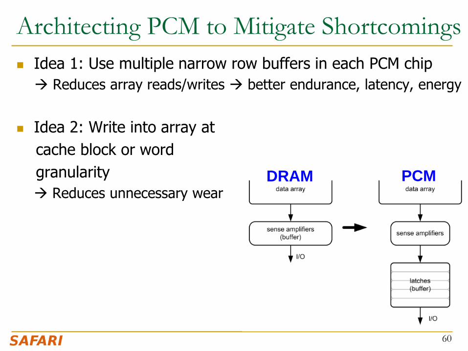
Architecting PCM to Mitigate Shortcomings
Idea 1: Use multiple narrow row buffers in each PCM chip
Reduces array reads/writes better endurance, latency, energy
Idea 2: Write into array at
cache block or word
granularity
Reduces unnecessary wear
60
DRAM PCM

Results: Architected PCM as Main Memory
1.2x delay, 1.0x energy, 5.6-year average lifetime
Scaling improves energy, endurance, density
Caveat 1: Worst-case lifetime is much shorter (no guarantees)
Caveat 2: Intensive applications see large performance and energy hits
Caveat 3: Optimistic PCM parameters? 61

Hybrid Memory Systems
Meza+, “Enabling Efficient and Scalable Hybrid Memories,” IEEE Comp. Arch. Letters, 2012.
Yoon, Meza et al., “Row Buffer Locality Aware Caching Policies for Hybrid Memories,” ICCD 2012 Best Paper Award.
CPU DRAMCtrl
Fast, durable Small,
leaky, volatile, high-cost
Large, non-volatile, low-cost Slow, wears out, high active energy
PCM Ctrl DRAM Phase Change Memory (or Tech. X)
Hardware/software manage data allocation and movement to achieve the best of multiple technologies

One Option: DRAM as a Cache for PCM
PCM is main memory; DRAM caches memory rows/blocks
Benefits: Reduced latency on DRAM cache hit; write filtering
Memory controller hardware manages the DRAM cache
Benefit: Eliminates system software overhead
Three issues:
What data should be placed in DRAM versus kept in PCM?
What is the granularity of data movement?
How to design a huge (DRAM) cache at low cost?
Two solutions:
Locality-aware data placement [Yoon+ , ICCD 2012]
Cheap tag stores and dynamic granularity [Meza+, IEEE CAL 2012]
63

DRAM vs. PCM: An Observation
Row buffers are the same in DRAM and PCM
Row buffer hit latency same in DRAM and PCM
Row buffer miss latency small in DRAM, large in PCM
Accessing the row buffer in PCM is fast
What incurs high latency is the PCM array access avoid this
64
CPU DRAMCtrl
PCM Ctrl
Bank
Bank
Bank
Bank
Row buffer DRAM Cache PCM Main Memory
N ns row hit Fast row miss
N ns row hit Slow row miss

Row-Locality-Aware Data Placement
Idea: Cache in DRAM only those rows that
Frequently cause row buffer conflicts because row-conflict latency
is smaller in DRAM
Are reused many times to reduce cache pollution and bandwidth waste
Simplified rule of thumb:
Streaming accesses: Better to place in PCM
Other accesses (with some reuse): Better to place in DRAM
Yoon et al., “Row Buffer Locality-Aware Data Placement in Hybrid Memories,” ICCD 2012 Best Paper Award.
65

Row-Locality-Aware Data Placement: Results
66
0
0.2
0.4
0.6
0.8
1
1.2
1.4
Server Cloud Avg
No
rmali
zed
Wei
gh
ted
Sp
eed
up
Workload
FREQ FREQ-Dyn RBLA RBLA-Dyn
10% 14% 17%
Memory energy-efficiency and fairness also improve correspondingly

0
0.2
0.4
0.6
0.8
1
1.2
1.4
1.6
1.8
2
Weighted Speedup Max. Slowdown Perf. per Watt
Normalized Metric
16GB PCM RBLA-Dyn 16GB DRAM
0
0.2
0.4
0.6
0.8
1
1.2
1.4
1.6
1.8
2
No
rma
lize
d W
eig
hte
d S
pee
du
p
0
0.2
0.4
0.6
0.8
1
1.2
No
rma
lize
d M
ax
. S
low
dow
n
Hybrid vs. All-PCM/DRAM
67
31% better performance than all PCM, within 29% of all DRAM performance
31%
29%

Aside: STT-RAM as Main Memory
Magnetic Tunnel Junction (MTJ)
Reference layer: Fixed
Free layer: Parallel or anti-parallel
Cell
Access transistor, bit/sense lines
Read and Write
Read: Apply a small voltage across bitline and senseline; read the current.
Write: Push large current through MTJ. Direction of current determines new orientation of the free layer.
Kultursay et al., “Evaluating STT-RAM as an
Energy-Efficient Main Memory Alternative,” ISPASS 2013.
Reference Layer
Free Layer
Barrier
Reference Layer
Free Layer
Barrier
Logical 0
Logical 1
Word Line
Bit Line
Access Transistor
MTJ
Sense Line

Aside: STT-RAM: Pros and Cons
Pros over DRAM
Better technology scaling
Non volatility
Low idle power (no refresh)
Cons
Higher write latency
Higher write energy
Reliability?
Another level of freedom
Can trade off non-volatility for lower write latency/energy (by reducing the size of the MTJ)
69

Architected STT-RAM as Main Memory
4-core, 4GB main memory, multiprogrammed workloads
~6% performance loss, ~60% energy savings vs. DRAM
70
88%
90%
92%
94%
96%
98%
Pe
rfo
rma
nce
vs.
DR
AM
STT-RAM (base) STT-RAM (opt)
0%
20%
40%
60%
80%
100%
En
erg
y
vs.
DR
AM
ACT+PRE WB RB
Kultursay+, “Evaluating STT-RAM as an Energy-Efficient Main Memory Alternative,” ISPASS 2013.

Agenda
Major Trends Affecting Main Memory
The Memory Scaling Problem and Solution Directions
New Memory Architectures
Enabling Emerging Technologies: Hybrid Memory Systems
How Can We Do Better?
Summary
71

Principles (So Far)
Better cooperation between devices and the system
Expose more information about devices to upper layers
More flexible interfaces
Better-than-worst-case design
Do not optimize for the worst case
Worst case should not determine the common case
Heterogeneity in design
Enables a more efficient design (No one size fits all)
72

Other Opportunities with Emerging Technologies
Merging of memory and storage
e.g., a single interface to manage all data
New applications
e.g., ultra-fast checkpoint and restore
More robust system design
e.g., reducing data loss
Processing tightly-coupled with memory
e.g., enabling efficient search and filtering
73

Coordinated Memory and Storage with NVM (I)
The traditional two-level storage model is a bottleneck with NVM Volatile data in memory a load/store interface
Persistent data in storage a file system interface
Problem: Operating system (OS) and file system (FS) code to locate, translate, buffer data become performance and energy bottlenecks with fast NVM stores
74
Two-Level Store
Processor and caches
Main Memory Storage (SSD/HDD)
Virtual memory
Address translation
Load/Store
Operating system
and file system
fopen, fread, fwrite, …

Coordinated Memory and Storage with NVM (II)
Goal: Unify memory and storage management in a single unit to eliminate wasted work to locate, transfer, and translate data
Improves both energy and performance
Simplifies programming model as well
75
Unified Memory/Storage
Processor and caches
Persistent (e.g., Phase-Change) Memory
Load/Store
Persistent Memory Manager
Feedback
Meza+, “A Case for Efficient Hardware-Software Cooperative Management of Storage and Memory,” WEED 2013.

The Persistent Memory Manager (PMM)
Exposes a load/store interface to access persistent data
Applications can directly access persistent memory no conversion,
translation, location overhead for persistent data
Manages data placement, location, persistence, security
To get the best of multiple forms of storage
Manages metadata storage and retrieval
This can lead to overheads that need to be managed
Exposes hooks and interfaces for system software
To enable better data placement and management decisions
Meza+, “A Case for Efficient Hardware-Software Cooperative Management of Storage and Memory,” WEED 2013.
76

The Persistent Memory Manager (PMM)
77
PMM uses access and hint information to allocate, locate, migrate and access data in the heterogeneous array of devices
Persistent objects

Performance Benefits of a Single-Level Store
78 Results for PostMark
~5X
~24X

Energy Benefits of a Single-Level Store
79 Results for PostMark
~5X
~16X

Agenda
Major Trends Affecting Main Memory
The Memory Scaling Problem and Solution Directions
New Memory Architectures
Enabling Emerging Technologies: Hybrid Memory Systems
How Can We Do Better?
Summary
80

Summary: Memory/Storage Scaling
Memory/storage scaling problems are a critical bottleneck for system performance, efficiency, and usability
New memory/storage + compute architectures Rethinking DRAM; processing close to data; accelerating bulk operations
Ensuring memory/storage reliability and robustness
Enabling emerging NVM technologies Hybrid memory systems with automatic data management
Coordinated management of memory and storage with NVM
System-level memory/storage QoS QoS-aware controller and system design
Coordinated memory + storage QoS
Software/hardware/device cooperation essential
81

Related Posters Today
RowClone: Accelerating Page Copy and Initialization in DRAM
Vivek Seshadri
Linearly Compressed Pages and Base-Delta-Immediate Compression: Efficient Memory Compression
Gennady Pekhimenko
Single-Level NVM Stores: Hardware-Software Cooperative Management of Storage and Memory
Samira Khan
82

More Material: Slides, Papers, Videos
These slides are a very short version of the Scalable Memory Systems course at ACACES 2013
Website for Course Slides, Papers, and Videos
http://users.ece.cmu.edu/~omutlu/acaces2013-memory.html
http://users.ece.cmu.edu/~omutlu/projects.htm
Includes extended lecture notes and readings
Overview Reading
Onur Mutlu, "Memory Scaling: A Systems Architecture Perspective" Technical talk at MemCon 2013 (MEMCON), Santa Clara, CA, August 2013. Slides (pptx) (pdf)
83

Thank you.
Feel free to email me with any questions & feedback
84

Rethinking Memory System Design for
Data-Intensive Computing
Onur Mutlu
December 6, 2013
IAP Cloud Workshop

Three Key Problems in Systems
The memory system
Data storage and movement limit performance & efficiency
Efficiency (performance and energy) scalability
Efficiency limits performance & scalability
Predictability and robustness
Predictable performance and QoS become first class constraints as systems scale in size and technology
86

Summary: Memory/Storage Scaling Main memory scaling problems are a critical bottleneck for
system performance, efficiency, and usability
Solution 1: Tolerate DRAM with novel architectures RAIDR: Retention-aware refresh
TL-DRAM: Tiered-Latency DRAM
RowClone: Fast page copy and initialization
SALP: Subarray-level parallelism
BDI and LCP: Efficient memory compression
Solution 2: Enable emerging memory technologies Replace DRAM with NVM by architecting NVM chips well
Hybrid memory systems with automatic data management
Coordinated management of memory and storage
Software/hardware/device cooperation essential for effective scaling of main memory
87

Tolerating DRAM: Example Techniques
Retention-Aware DRAM Refresh: Reducing Refresh Impact
Tiered-Latency DRAM: Reducing DRAM Latency
RowClone: Accelerating Page Copy and Initialization
Subarray-Level Parallelism: Reducing Bank Conflict Impact
Linearly Compressed Pages: Efficient Memory Compression
88

SALP: Reducing DRAM Bank Conflicts
Problem: Bank conflicts are costly for performance and energy
serialized requests, wasted energy (thrashing of row buffer, busy wait)
Goal: Reduce bank conflicts without adding more banks (low cost)
Key idea: Exploit the internal subarray structure of a DRAM bank to parallelize bank conflicts to different subarrays
Slightly modify DRAM bank to reduce subarray-level hardware sharing
Results on Server, Stream/Random, SPEC
19% reduction in dynamic DRAM energy
13% improvement in row hit rate
17% performance improvement
0.15% DRAM area overhead
89 Kim, Seshadri+ “A Case for Exploiting Subarray-Level
Parallelism in DRAM,” ISCA 2012. 0.0
0.2
0.4
0.6
0.8
1.0
1.2
No
rma
lize
d
Dyn
am
ic E
ne
rgy
Baseline MASA
-19
%
0%
20%
40%
60%
80%
100%
Ro
w-B
uff
er
Hit
-…
Baseline MASA
+1
3%

Tolerating DRAM: Example Techniques
Retention-Aware DRAM Refresh: Reducing Refresh Impact
Tiered-Latency DRAM: Reducing DRAM Latency
RowClone: Accelerating Page Copy and Initialization
Subarray-Level Parallelism: Reducing Bank Conflict Impact
Linearly Compressed Pages: Efficient Memory Compression
90

Efficient Memory Compression: Summary
Idea: Compress redundant data in main memory
Problem 1: How to minimize decompression latency?
Problem 2: How to avoid latency increase to find a compressed cache block in a page?
Solution 1: Base-Delta-Immediate Compression [PACT’12]
Encode data as base value + small deltas from that base
Solution 2: Linearly Compressed Pages (LCP) [MICRO’13]
Fixed-size cache block granularity compression
New page format that separates compressed data, uncompressed data, metadata
Results:
Increases memory capacity (69% on average)
Decreases memory bandwidth consumption (24%)
Improves performance (13.7%) and memory energy (9.5%)
91

End of Backup Slides
92
Related Documents