May 10, 2014 R.Innocente 1 Reconfigurable Computing Reconfigurable Computing Roberto Innocente [email protected] Part 1 of 2

Welcome message from author
This document is posted to help you gain knowledge. Please leave a comment to let me know what you think about it! Share it to your friends and learn new things together.
Transcript

May 10, 2014 R.Innocente 1
Reconfigurable ComputingReconfigurable Computing
Roberto Innocente
Part 1 of 2

May 10, 2014 R.Innocente 2
Flexibility
ASICApplication
SpecificIntegrated Circuit
Very inflexible,designed to solve just 1 problem.Energy, space and time
efficient
GPPGeneralPurpose
Processor
Very flexible,can solve any problem. Energy, space and time
inefficient
?
ReconfigurableHardwareFlexible,
But enough energy, time and space efficient
+-
May 10, 2014 R.Innocente 3
History
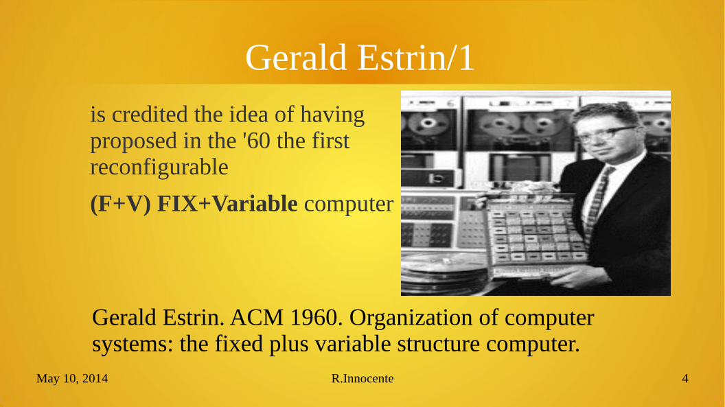
May 10, 2014 R.Innocente 4
Gerald Estrin/1is credited the idea of having proposed in the '60 the first reconfigurable
(F+V) FIX+Variable computer
Gerald Estrin. ACM 1960. Organization of computer systems: the fixed plus variable structure computer.

May 10, 2014 R.Innocente 5
Gerald Estrin/2He envisioned that important gains in performance could be achieved when many computations are executed on appropriate problem oriented configurations.
F+V is made of :
- high speed general computer(the F part) : initially an ibm7090
- various size high speed special structures (the V part) problem specific: trigonometric functions, logarithms, exponential, n-th powers, complex arithmetic, …
V is made of a 36 module positions motherboard which can undergo :
- Function reconfiguration: physically changing some modules
- Routing reconfiguration : changing part of the back wiring
The Rammig machine (1977) : investigation of a reconfigurable machine with no manual or mechanical intervention
May 10, 2014 R.Innocente 6
Today reconfigurable hardware
Is born out of the will to replace different logic IC(Integrated Circuits), and successively to rapidly prototype large ASICs(Application Specific ICs) or implement SoCs (Sytem On Chip).
In the following slides readers are supposed to be involved in scientific computing and not EE engineers.

May 10, 2014 R.Innocente 7
Basic digital circuitsAND INVERTER
Shift RegD Type FFMUX
Usually 0=0V, 1=some positive voltage
OR

May 10, 2014 R.Innocente 8
SSI 74xx IC
May 10, 2014 R.Innocente 9
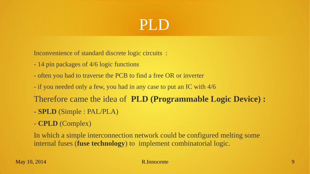
PLD
Inconvenience of standard discrete logic circuits :
- 14 pin packages of 4/6 logic functions
- often you had to traverse the PCB to find a free OR or inverter
- if you needed only a few, you had in any case to put an IC with 4/6
Therefore came the idea of PLD (Programmable Logic Device) :
- SPLD (Simple : PAL/PLA)
- CPLD (Complex)
In which a simple interconnection network could be configured melting some internal fuses (fuse technology) to implement combinatorial logic.

May 10, 2014 R.Innocente 10
disjunctive normal form(aka Sum of products )
Each boolean function of some boolean variables can be represented as a sum of minterms (product of all variables or their complement) .
With 3 boolean vars : a,b,c
are 2 of the 23 = 8 minterms
f (a ,b , c)=a b c+a b c
a b c , a b c

May 10, 2014 R.Innocente 11
PLA (Programmable Logic Array)
f1=p1+ p2+ p3=x1x2+x1 x3+ x1 x2 x3+x1 x3

May 10, 2014 R.Innocente 12
FPGAAlso CPLDs showed their limits, therefore in 1985/1990 Xilinx introduced a more flexible design , the
FPGA (Field Programmable Gate Array)
In which the interconnection network is much more flexible and on which also sequential circuits can be easily mapped.

May 10, 2014 R.Innocente 13
FPGA idea1985 Xilinx – Ross Freeman (inventor of FPGA): “What if we could develop the equivalent of a circuit board full of standard logic parts (like TTL and PAL devices) on a single high density programmable logic chip ?”
- post fabrication programmability by end users
- fabless semiconductor company
May 10, 2014 R.Innocente 14
Today
May 10, 2014 R.Innocente 15
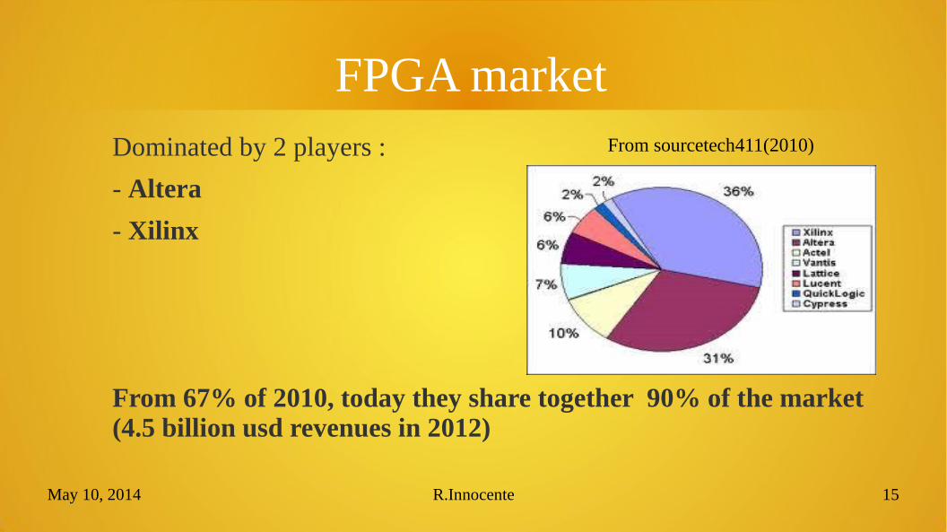
FPGA marketDominated by 2 players :
- Altera
- Xilinx
From 67% of 2010, today they share together 90% of the market (4.5 billion usd revenues in 2012)
From sourcetech411(2010)

May 10, 2014 R.Innocente 16
An important question: are FPGAs green ?
Virtex-7 2000T (one of the top FPGAs) :
~ 20 WXilinx showed 3600 copies of its 8 bit processor nanoblaze running on Virtex-7, consuming 20 W
CPU : ~ 100 WCore i7-4770K Haswell (22 nm) 3.5 GHz@ 4 Cores 84 W
Core i7-3930K Sandybridge-E (32 nm) 3.2 GHz @6Cores 130 W
Xeon E7458 Dunnington (45 nm) 2.4 GHz 90 W
Xeon E7460 Dunnington (45 nm) 2.66 GHz 130 W
GPU : ~ 220 WNvidia Tesla M2090 225 W
Nvidia Tesla K20X 235 W
This is a partial answer. We need to be able to estimate FPGA performance to give a more useful index.

May 10, 2014 R.Innocente 17
FPGA architecture
From RF and Wireless World
Sea of gates : logic blocks are like islands in a sea of interconnections

May 10, 2014 R.Innocente 18
Virtex family1998 Virtex 250nm 100mhz 25k-60k cells
2000 Virtex-E 180nm 300mhz 1k-70kcells
2000 Virtex II 150nm to168 mult420mhzupto 93k 4-luts
2005 Virtex-4 90nm 500mhz upto 200k cells
2007 Virtex-5 65nm 550mhz up to 330k cells
Virtex-6 40nm 288-2k DSP to 500k 6-luts
2010 Virtex-7 28nm ~500mhz upto 2000k cells
2014 Virtex-US 20 nm upto 4400k cells
From L Zhuo
Up to ~ 7 billion transistorIntel 2014 15-core Xeon IvyBridge-EX~ 4.3 billion transistorNvidia 2012 GK110 Kepler ~ 7 billion transistor

May 10, 2014 R.Innocente 19
FPGA/CPU evolution
May 10, 2014 R.Innocente 20
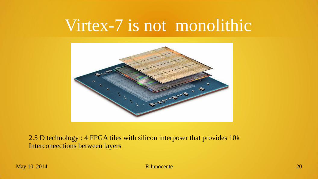
Virtex-7 is not monolithic
2.5 D technology : 4 FPGA tiles with silicon interposer that provides 10kInterconeections between layers

May 10, 2014 R.Innocente 21
Enabling technologies
May 10, 2014 R.Innocente 22
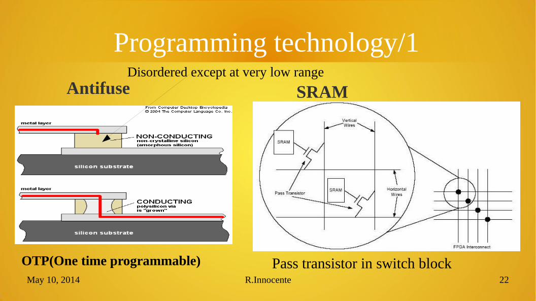
Programming technology/1
Antifuse SRAM
OTP(One time programmable)
Disordered except at very low range
Pass transistor in switch block

May 10, 2014 R.Innocente 23
Programming technology/2Antifuse
-pros:
cheap, small
-cons:
requires special processing, One time programming
SRAM
-pros:
can be deployed with standard semiconductor process, can be easily reprogrammed
-cons:
large area required(6 transistors)

May 10, 2014 R.Innocente 24
ConfwareThe configuration of an FPGA ( that becomes compiled to a stream of bits) is not hardware, nor software.
Someone invented the neologism
confware
The configuration of a reconfigurable hardware.
May 10, 2014 R.Innocente 25
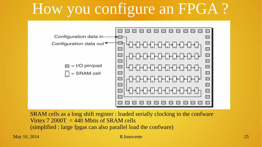
How you configure an FPGA ?
SRAM cells as a long shift register : loaded serially clocking in the confwareVirtex 7 2000T = 440 Mbits of SRAM cells(simplified : large fpgas can also parallel load the confware)
May 10, 2014 R.Innocente 26
Logic Blocks/Logic Cells

May 10, 2014 R.Innocente 27
Fine/coarse grain logic blocksFrom :
- a single transistor (Crosspoint : went in bankrupcy)
- a logic gate
To :
- a complete processor (FPNA: field programmable node arrays)
NB. FPNA is also field programmable neural array
May 10, 2014 R.Innocente 28
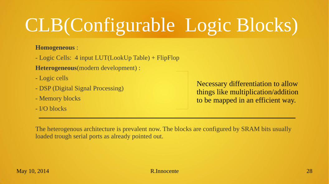
Homogeneous :
- Logic Cells: 4 input LUT(LookUp Table) + FlipFlop
Heterogeneous(modern development) :
- Logic cells
- DSP (Digital Signal Processing)
- Memory blocks
- I/O blocks
The heterogenous architecture is prevalent now. The blocks are configured by SRAM bits usually loaded trough serial ports as already pointed out.
CLB(Configurable Logic Blocks)
Necessary differentiation to allow things like multiplication/addition to be mapped in an efficient way.
May 10, 2014 R.Innocente 29
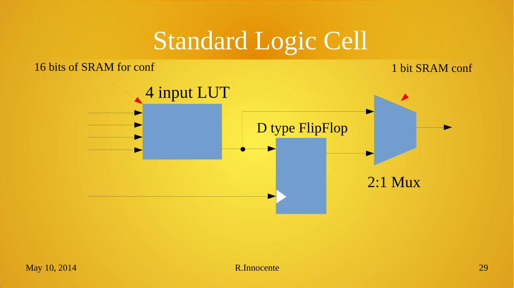
Standard Logic Cell
4 input LUT
D type FlipFlop
16 bits of SRAM for conf 1 bit SRAM conf
2:1 Mux

May 10, 2014 R.Innocente 30
standard LUT (Look Up Table)
0 0000 0
1 0001 1
2 0010 0
3 0011 0
4 0100 1
5 0101 0
6 0110 1
7 0111 1
.. .. ..
Dec Bin Out- 16 x 1 memory
- any boolean function of 4 inputs :
Bit 0
Bit 1
Bit 2
Bit 3
f = x3 x2 x1 x0+ x3 x2 x1 x0+ x3 x2 x1 x0+ x3 x2 x1 x0
NB. LUT rhymes with nut

May 10, 2014 R.Innocente 31
Uses of Logic Cell2^4 = 16 x 1 bit memory Any boolean function of 4
inputs
4:1 multiplexer

May 10, 2014 R.Innocente 32
Virtex-7 Logic Block basics
May 10, 2014 R.Innocente 33
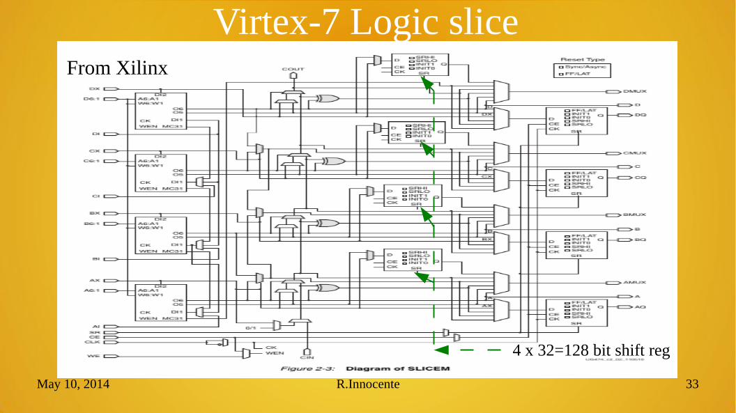
Virtex-7 Logic sliceFrom Xilinx
4 x 32=128 bit shift reg

May 10, 2014 R.Innocente 34
Virtex7 CLB slice- 6-input LUT
- 2 5-input LUTs with same inputs
- 2 arbitrary boolean function on 3-input and 2-input or less

May 10, 2014 R.Innocente 35
Altera ALM
May 10, 2014 R.Innocente 36
Interconnection network
May 10, 2014 R.Innocente 37
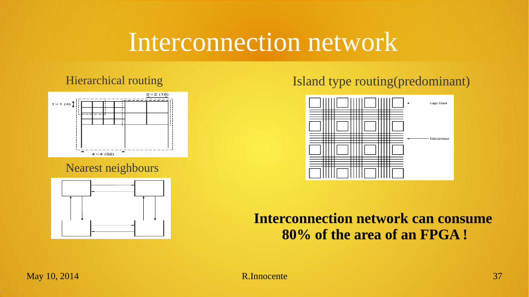
Interconnection networkHierarchical routing Island type routing(predominant)
Interconnection network can consume 80% of the area of an FPGA !
Nearest neighbours

May 10, 2014 R.Innocente 38
Programmable switch

May 10, 2014 R.Innocente 39
SRAM routing: coarse/fine grain5 bit SRAM 1 bit SRAM

May 10, 2014 R.Innocente 40
Details of island type routing
May 10, 2014 R.Innocente 41
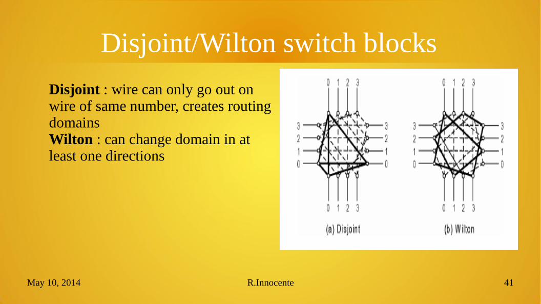
Disjoint/Wilton switch blocks
Disjoint : wire can only go out on wire of same number, creates routing domainsWilton : can change domain in at least one directions
May 10, 2014 R.Innocente 42
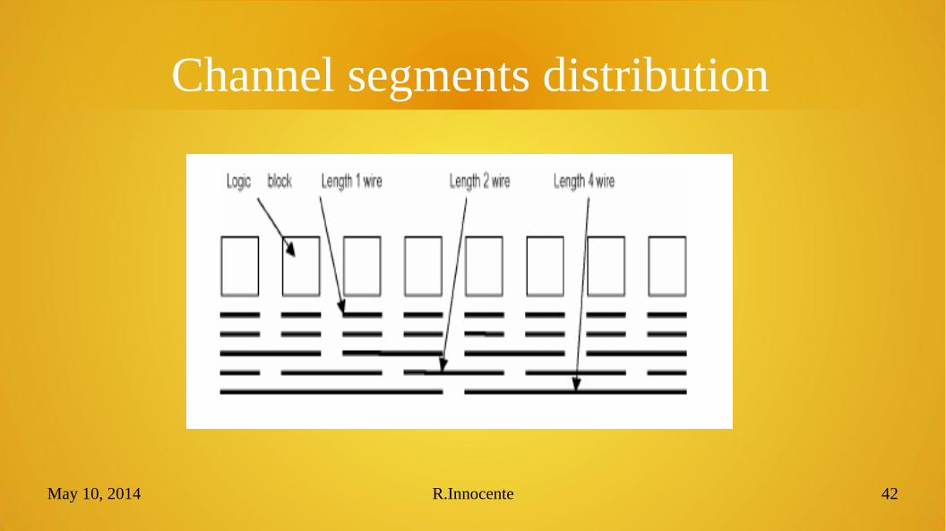
Channel segments distribution
May 10, 2014 R.Innocente 43
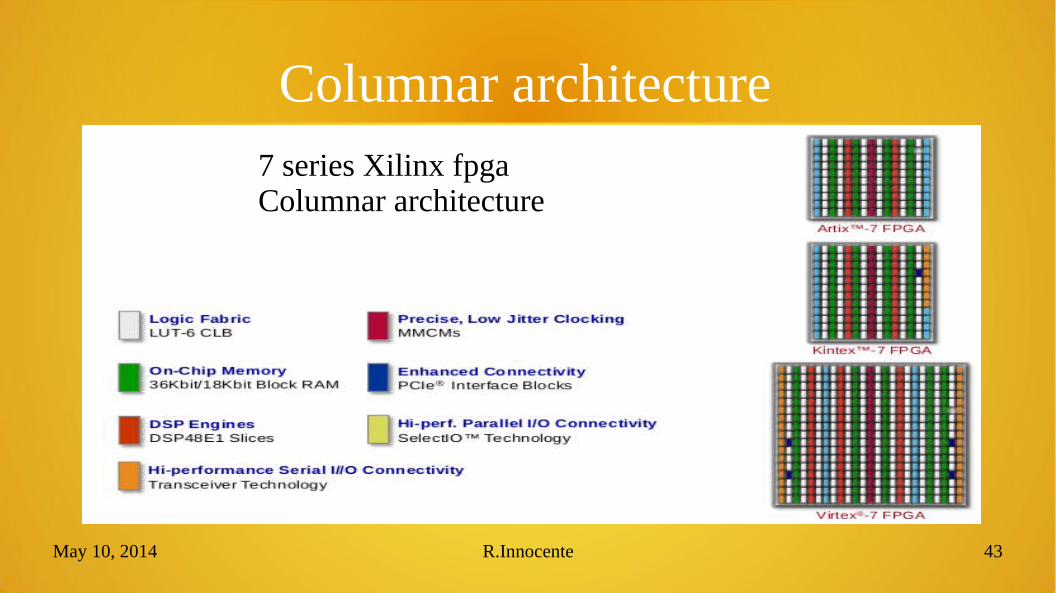
Columnar architecture7 series Xilinx fpgaColumnar architecture

May 10, 2014 R.Innocente 44
DSP blocks &floating point

May 10, 2014 R.Innocente 45
FPGAs floating point in 1994
B. Fagin and C. Renard. Field Programmable Gate Arrays and Floating Point Arithmetic. IEEE Transactions on VLSI Systems, 2(3), September 1994.
Fagin & Renard report that you can implement floating point operators but it is impractical : no
FPGA in existence could contain a single multiplier circuit !!
May 10, 2014 R.Innocente 46
FPGA fp in 1995Shirazi & al. On the same line of Fagin & Renard propose 2 custom fp formats 16 and 18 bits total:
they provide for them add,sub, mul, div operators
N. Shirazi, A. Walters, and P. Athanas. Quantitative Analysis of Floating Point Arithmetic on FPGA Based Custom Computing Machines. In Proceedings of the IEEE Symposium on FPGAs for Custom Computing Machines, April 1995.
May 10, 2014 R.Innocente 47
FPGA fp in 2002Belanovic & Leeser present a library of variable width parameterized floating point operators (superset of the ieee formats)
A Library of Parameterized Floating-point Modules and Their UsePavle Belanovic and Miriam Leeser, 2002
May 10, 2014 R.Innocente 48
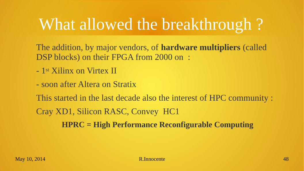
What allowed the breakthrough ?The addition, by major vendors, of hardware multipliers (called DSP blocks) on their FPGA from 2000 on :
- 1st Xilinx on Virtex II
- soon after Altera on Stratix
This started in the last decade also the interest of HPC community :
Cray XD1, Silicon RASC, Convey HC1
HPRC = High Performance Reconfigurable Computing
May 10, 2014 R.Innocente 49
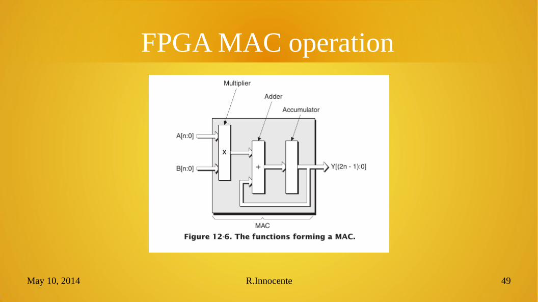
FPGA MAC operation

May 10, 2014 R.Innocente 50
Virtex-7 DSP48 high level
From Xilinx
1 bit 2 bit
May 10, 2014 R.Innocente 51
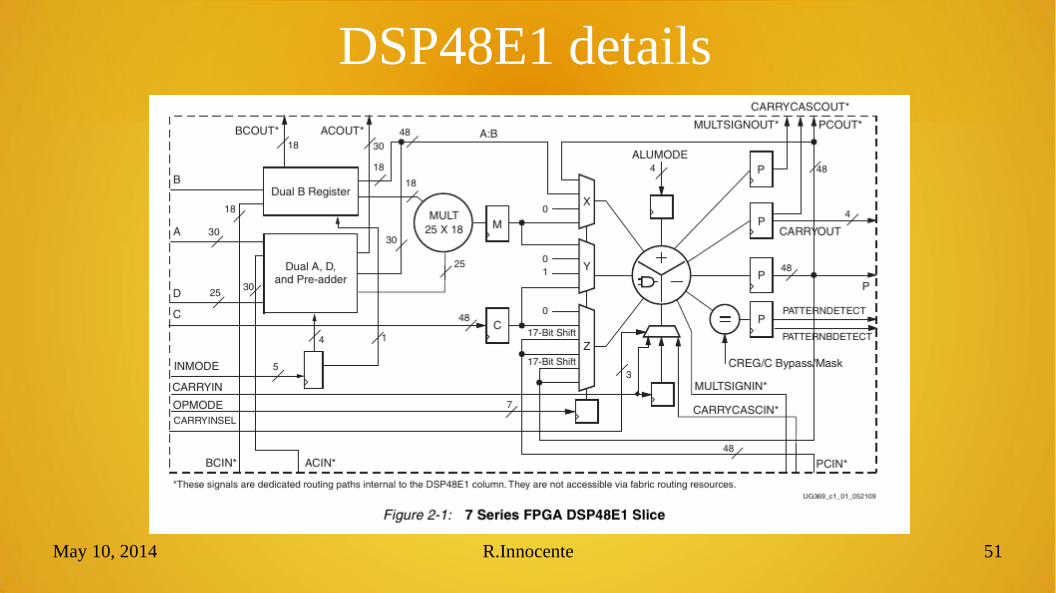
DSP48E1 details
May 10, 2014 R.Innocente 52
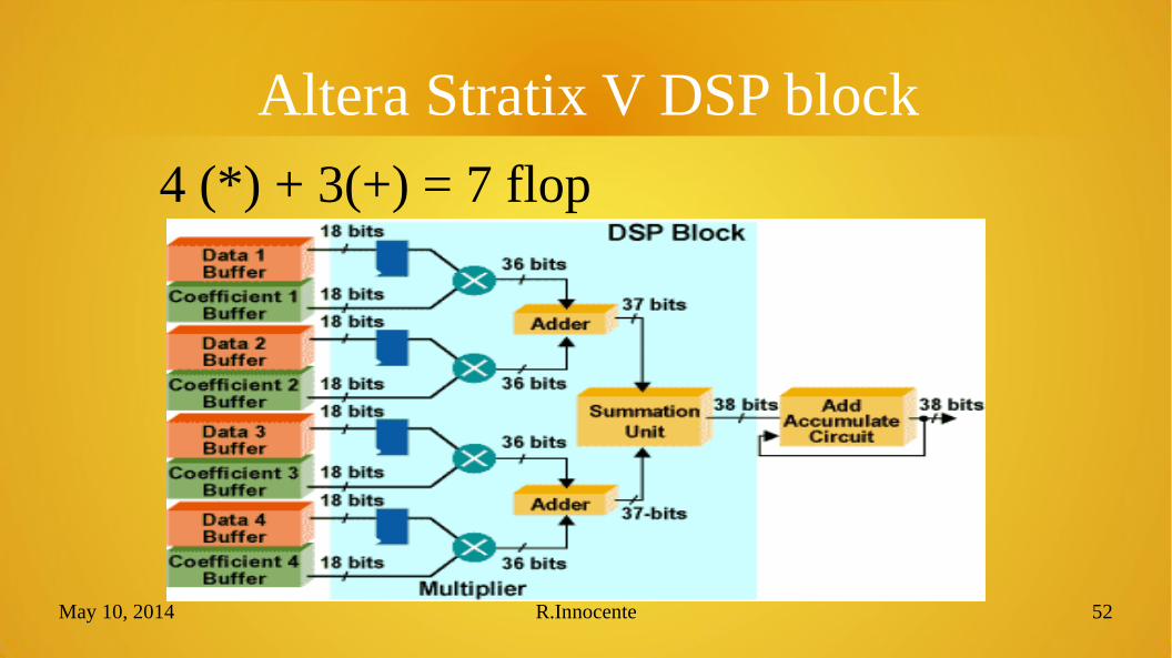
Altera Stratix V DSP block
4 (*) + 3(+) = 7 flop
May 10, 2014 R.Innocente 53
Data Flow Graphs (DFG)

May 10, 2014 R.Innocente 54
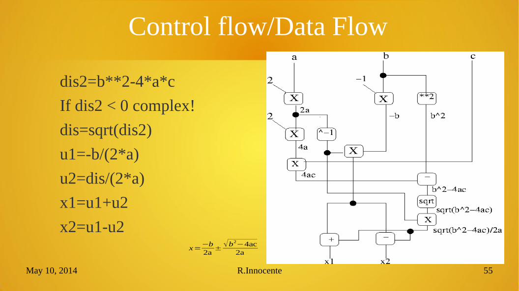
Data flowA representation of a program as a DG(Directed Graph) in which the nodes are the operations and the edges represent the data dependencies from one operation to the next
May 10, 2014 R.Innocente 55
Control flow/Data Flow
dis2=b**2-4*a*c
If dis2 < 0 complex!
dis=sqrt(dis2)
u1=-b/(2*a)
u2=dis/(2*a)
x1=u1+u2
x2=u1-u2x=
−b2a
±√b2−4ac
2a
May 10, 2014 R.Innocente 56
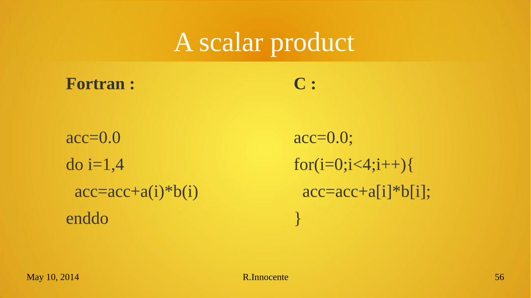
A scalar productFortran :
acc=0.0
do i=1,4
acc=acc+a(i)*b(i)
enddo
C :
acc=0.0;
for(i=0;i<4;i++){
acc=acc+a[i]*b[i];
}

May 10, 2014 R.Innocente 57
Time/Space tradeoffs
May 10, 2014 R.Innocente 58
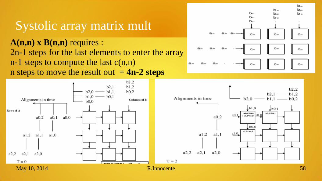
Systolic array matrix multA(n,n) x B(n,n) requires :2n-1 steps for the last elements to enter the arrayn-1 steps to compute the last c(n,n)n steps to move the result out = 4n-2 steps
May 10, 2014 R.Innocente 59
Codesign
The implementation of algorithms on FPGAs requires a mix of hw and sw design :
Codesign = hw design + sw design
May 10, 2014 R.Innocente 60
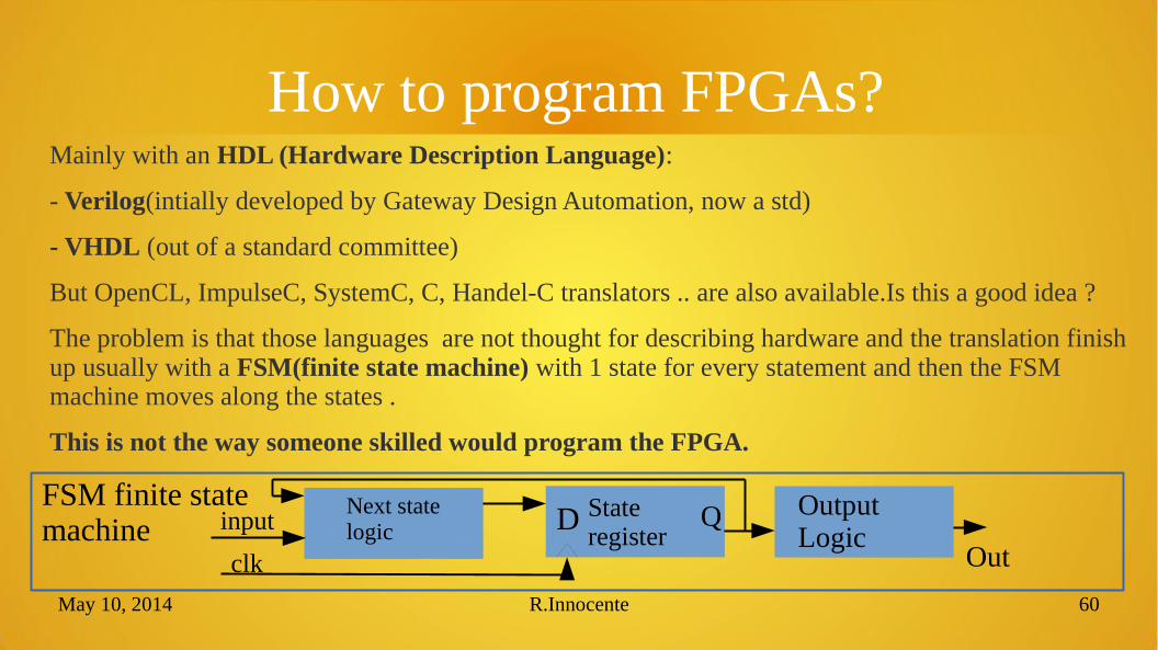
How to program FPGAs?Mainly with an HDL (Hardware Description Language):
- Verilog(intially developed by Gateway Design Automation, now a std)
- VHDL (out of a standard committee)
But OpenCL, ImpulseC, SystemC, C, Handel-C translators .. are also available.Is this a good idea ?
The problem is that those languages are not thought for describing hardware and the translation finish up usually with a FSM(finite state machine) with 1 state for every statement and then the FSM machine moves along the states .
This is not the way someone skilled would program the FPGA.
Next statelogic
Stateregister
Output Logic
input
clk
D Q
Out
FSM finite state machine

May 10, 2014 R.Innocente 61
FPGA will winFor many years FPGAs were just prototyping vehicles for ASICs
– Now they are replacing many ASICS & ASSPs
– Watch for the same Trojan effect with FPGAs in HPC

May 10, 2014 R.Innocente 62
End of part 1 of 2
Related Documents