11 Recommended Design Practices 2014.06.30 QII51006 Subscribe Send Feedback This chapter provides design recommendations for Altera ® devices and describes the Quartus ® II Design Assistant, which helps you check your design for violations of Altera’s design recommendations. Current FPGA applications have reached the complexity and performance requirements of ASICs. In the development of complex system designs, good design practices have an enormous impact on the timing performance, logic utilization, and system reliability of a device. Well-coded designs behave in a predictable and reliable manner even when retargeted to different families or speed grades. Good design practices also aid in successful design migration between FPGA and ASIC implementations for prototyping and production. For optimal performance, reliability, and faster time-to-market when designing with Altera devices, you should adhere to the following guidelines: • Understand the impact of synchronous design practices • Follow recommended design techniques, including hierarchical design partitioning, and timing closure guidelines • Take advantage of the architectural features in the targeted device Following Synchronous FPGA Design Practices The first step in good design methodology is to understand the implications of your design practices and techniques. This section outlines the benefits of optimal synchronous design practices and the hazards involved in other techniques. Good synchronous design practices can help you meet your design goals consistently. Problems with other design techniques can include reliance on propagation delays in a device, which can lead to race conditions, incomplete timing analysis, and possible glitches. In a synchronous design, a clock signal triggers every event. As long as you ensure that all the timing requirements of the registers are met, a synchronous design behaves in a predictable and reliable manner for all process, voltage, and temperature (PVT) conditions. You can easily migrate synchronous designs to different device families or speed grades. Implementing Synchronous Designs In a synchronous design, the clock signal controls the activities of all inputs and outputs. On every active edge of the clock (usually the rising edge), the data inputs of registers are sampled and transferred to outputs. Following an active clock edge, the outputs of combinational logic feeding the data inputs of registers change values. This change triggers a period of instability due to propagation delays ISO 9001:2008 Registered © 2014 Altera Corporation. All rights reserved. ALTERA, ARRIA, CYCLONE, ENPIRION, MAX, MEGACORE, NIOS, QUARTUS and STRATIX words and logos are trademarks of Altera Corporation and registered in the U.S. Patent and Trademark Office and in other countries. All other words and logos identified as trademarks or service marks are the property of their respective holders as described at www.altera.com/common/legal.html. Altera warrants performance of its semiconductor products to current specifications in accordance with Altera's standard warranty, but reserves the right to make changes to any products and services at any time without notice. Altera assumes no responsibility or liability arising out of the application or use of any information, product, or service described herein except as expressly agreed to in writing by Altera. Altera customers are advised to obtain the latest version of device specifications before relying on any published information and before placing orders for products or services. www.altera.com 101 Innovation Drive, San Jose, CA 95134

Welcome message from author
This document is posted to help you gain knowledge. Please leave a comment to let me know what you think about it! Share it to your friends and learn new things together.
Transcript
11Recommended Design Practices
2014.06.30
QII51006 Subscribe Send Feedback
This chapter provides design recommendations for Altera® devices and describes the Quartus® II DesignAssistant, which helps you check your design for violations of Altera’s design recommendations.
Current FPGA applications have reached the complexity and performance requirements of ASICs. In thedevelopment of complex system designs, good design practices have an enormous impact on the timingperformance, logic utilization, and system reliability of a device. Well-coded designs behave in a predictableand reliable manner even when retargeted to different families or speed grades. Good design practices alsoaid in successful designmigration between FPGAandASIC implementations for prototyping and production.
For optimal performance, reliability, and faster time-to-market when designing with Altera devices, youshould adhere to the following guidelines:
• Understand the impact of synchronous design practices• Follow recommended design techniques, including hierarchical design partitioning, and timing closure
guidelines• Take advantage of the architectural features in the targeted device
Following Synchronous FPGA Design PracticesThe first step in good design methodology is to understand the implications of your design practices andtechniques. This section outlines the benefits of optimal synchronous design practices and the hazardsinvolved in other techniques.
Good synchronous design practices can help you meet your design goals consistently. Problems with otherdesign techniques can include reliance on propagation delays in a device, which can lead to race conditions,incomplete timing analysis, and possible glitches.
In a synchronous design, a clock signal triggers every event. As long as you ensure that all the timingrequirements of the registers are met, a synchronous design behaves in a predictable and reliable mannerfor all process, voltage, and temperature (PVT) conditions. You can easily migrate synchronous designs todifferent device families or speed grades.
Implementing Synchronous DesignsIn a synchronous design, the clock signal controls the activities of all inputs and outputs.
On every active edge of the clock (usually the rising edge), the data inputs of registers are sampled andtransferred to outputs. Following an active clock edge, the outputs of combinational logic feeding the datainputs of registers change values. This change triggers a period of instability due to propagation delays
ISO9001:2008Registered
© 2014 Altera Corporation. All rights reserved. ALTERA, ARRIA, CYCLONE, ENPIRION, MAX, MEGACORE, NIOS, QUARTUS and STRATIX wordsand logos are trademarks of Altera Corporation and registered in the U.S. Patent and Trademark Office and in other countries. All otherwords and logos identified as trademarks or service marks are the property of their respective holders as described atwww.altera.com/common/legal.html. Altera warrants performance of its semiconductor products to current specifications in accordance withAltera's standard warranty, but reserves the right to make changes to any products and services at any time without notice. Altera assumesno responsibility or liability arising out of the application or use of any information, product, or service described herein except as expresslyagreed to in writing by Altera. Altera customers are advised to obtain the latest version of device specifications before relying on any publishedinformation and before placing orders for products or services.
www.altera.com
101 Innovation Drive, San Jose, CA 95134
through the logic as the signals go through several transitions and finally settle to new values. Changes thatoccur on data inputs of registers do not affect the values of their outputs until after the next active clockedge.
Because the internal circuitry of registers isolates data outputs from inputs, instability in the combinationallogic does not affect the operation of the design as long as you meet the following timing requirements:
• Before an active clock edge, you must ensure that the data input has been stable for at least the setup timeof the register.
• After an active clock edge, you must ensure that the data input remains stable for at least the hold timeof the register.
When you specify all of your clock frequencies and other timing requirements, theQuartus II TimeQuestTiming Analyzer reports actual hardware requirements for the setup times (tSU) and hold times (tH) forevery pin in your design. By meeting these external pin requirements and following synchronous designtechniques, you ensure that you satisfy the setup and hold times for all registers in your device.
To meet setup and hold time requirements on all input pins, any inputs to combinational logicthat feed a register should have a synchronous relationship with the clock of the register. If signalsare asynchronous, you can register the signals at the inputs of the device to help prevent a violationof the required setup and hold times.
When you violate the setup or hold time of a register, you might oscillate the output, or set theoutput to an intermediate voltage level between the high and low levels called a metastable state.In this unstable state, small perturbations such as noise in power rails can cause the register toassume either the high or low voltage level, resulting in an unpredictable valid state. Variousundesirable effects can occur, including increased propagation delays and incorrect output states.In some cases, the output can even oscillate between the two valid states for a relatively long periodof time.
Tip:
Related InformationAbout TimeQuest Timing AnalysisFor information about timing requirements and analysis in theQuartus II software, refer toAbout TimeQuestTiming Analysis in Quartus II Help.
Asynchronous Design HazardsDesigners use asynchronous techniques such as ripple counters or pulse generators in programmable logicdevice (PLD) designs, enabling them to take “short cuts” to save device resources.
Asynchronous design techniques have inherent problems such as relying on propagation delays in a device,which can vary with temperature and voltage fluctuations, resulting in incomplete timing constraints andpossible glitches and spikes.
Some asynchronous design structures rely on the relative propagation delays of signals to function correctly.In these cases, race conditions can arise where the order of signal changes can affect the output of the logic.PLD designs can have varying timing delays, depending on how the design is placed and routed in the devicewith each compilation. Therefore, it is almost impossible to determine the timing delay associated with aparticular block of logic ahead of time. As devices become faster due to device process improvements, thedelays in an asynchronous design may decrease, resulting in a design that does not function as expected.This chapter provides specific examples. Relying on a particular delay also makes asynchronous designsdifficult to migrate to different architectures, devices, or speed grades.
The timing of asynchronous design structures is often difficult or impossible tomodelwith timing assignmentsand constraints. If you do not have complete or accurate timing constraints, the timing-driven algorithms
Recommended Design PracticesAltera Corporation
Send Feedback
QII51006Asynchronous Design Hazards11-2 2014.06.30
used by your synthesis and place-and-route tools may not be able to perform the best optimizations, andthe reported results may not be complete.
Some asynchronous design structures can generate harmful glitches, which are pulses that are very shortcompared with clock periods. Most glitches are generated by combinational logic. When the inputs ofcombinational logic change, the outputs exhibit several glitches before they settle to their new values. Theseglitches can propagate through the combinational logic, leading to incorrect values on the outputs inasynchronous designs. In a synchronous design, glitches on the data inputs of registers are normal eventsthat have no negative consequences because the data is not processed until the clock edge.
HDL Design GuidelinesWhen designing with HDL code, you should understand how a synthesis tool interprets different HDLdesign techniques and what results to expect.
Your design techniques can affect logic utilization and timing performance, as well as the design’s reliability.This section describes basic design techniques that ensure optimal synthesis results for designs targeted toAltera devices while avoiding several common causes of unreliability and instability. Altera recommendsthat you design your combinational logic carefully to avoid potential problems and pay attention to yourclocking schemes so that you can maintain synchronous functionality and avoid timing problems.
Optimizing Combinational LogicCombinational logic structures consist of logic functions that depend only on the current state of the inputs.In Altera FPGAs, these functions are implemented in the look-up tables (LUTs) with either logic elements(LEs) or adaptive logic modules (ALMs).
For cases where combinational logic feeds registers, the register control signals can implement part of thelogic function to save LUT resources. By following the recommendations in this section, you can improvethe reliability of your combinational design.
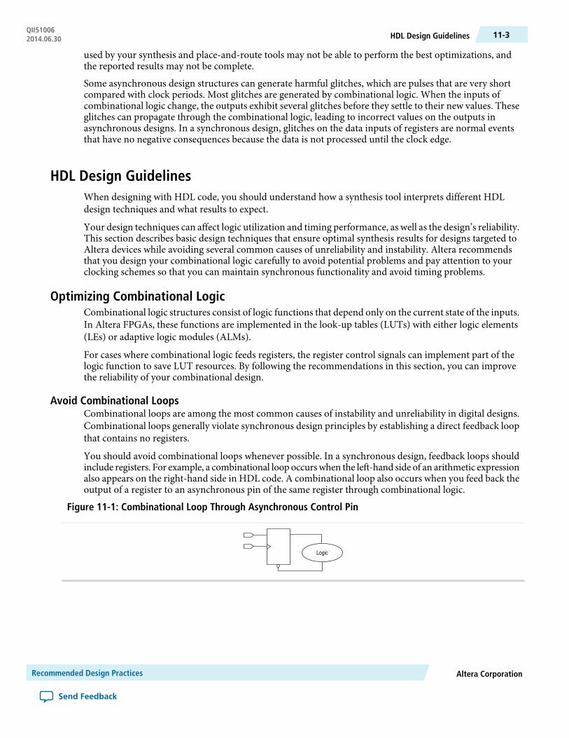
Avoid Combinational LoopsCombinational loops are among the most common causes of instability and unreliability in digital designs.Combinational loops generally violate synchronous design principles by establishing a direct feedback loopthat contains no registers.
You should avoid combinational loops whenever possible. In a synchronous design, feedback loops shouldinclude registers. For example, a combinational loop occurswhen the left-hand side of an arithmetic expressionalso appears on the right-hand side in HDL code. A combinational loop also occurs when you feed back theoutput of a register to an asynchronous pin of the same register through combinational logic.
Figure 11-1: Combinational Loop Through Asynchronous Control Pin
Logic
Altera CorporationRecommended Design Practices
Send Feedback
11-3HDL Design GuidelinesQII510062014.06.30
Use recovery and removal analysis to perform timing analysis on asynchronous ports, such as clearor reset in the Quartus II software.
Combinational loops are inherently high-risk design structures for the following reasons:
• Combinational loop behavior generally depends on relative propagation delays through the logicinvolved in the loop. As discussed, propagation delays can change, which means the behavior ofthe loop is unpredictable.
Tip:
• Combinational loops can cause endless computation loops in many design tools. Most tools breakopen combinational loops to process the design. The various tools used in the design flow mayopen a given loop in a different manner, processing it in a way that is inconsistent with the originaldesign intent.
Related InformationSpecifying Timing Constraints and Exceptions
Avoid Unintended Latch InferenceA latch is a small circuit with combinational feedback that holds a value until a new value is assigned. Youcan implement latches with the Quartus II Text Editor or Block Editor.
It is common for mistakes in HDL code to cause unintended latch inference; Quartus II Synthesis issues awarning message if this occurs. Unlike other technologies, a latch in FPGA architecture is not significantlysmaller than a register. The architecture is not optimized for latch implementation and latches generallyhave slower timing performance compared to equivalent registered circuitry.
Latches have a transparent mode in which data flows continuously from input to output. A positive latch isin transparent mode when the enable signal is high (low for negative latch). In transparent mode, glitcheson the input can pass through to the output because of the direct path created. This presents significantcomplexity for timing analysis. Typical latch schemes usemultiple enable phases to prevent long transparentpaths from occurring. However, timing analysis cannot identify these safe applications.
The TimeQuest analyzer analyzes latches as synchronous elements clocked on the falling edge of the positivelatch signal by default, and allows you to treat latches as having nontransparent start and end points. Beaware that even an instantaneous transition through transparent mode can lead to glitch propagation. TheTimeQuest analyzer cannot perform cycle-borrowing analysis.
Due to various timing complexities, latches have limited support in formal verification tools. Therefore, youshould not rely on formal verification for a design that includes latches.
Avoid using latches to ensure that you can completely analyze the timing performance and reliabilityof your design.
Tip:
Avoid Delay Chains in Clock PathsYou require delay chains when you use two or more consecutive nodes with a single fan-in and a singlefan-out to cause delay. Inverters are often chained together to add delay. Delay chains are sometimes usedto resolve race conditions created by other asynchronous design practices.
Delays in PLD designs can change with each placement and routing cycle. Effects such as rise and fall timedifferences and on-chip variation mean that delay chains, especially those placed on clock paths, can causesignificant problems in your design. Avoid using delay chains to prevent these kinds of problems.
In some ASIC designs, delays are used for buffering signals as they are routed around the device. Thisfunctionality is not required in FPGA devices because the routing structure provides buffers throughout thedevice.
Recommended Design PracticesAltera Corporation
Send Feedback
QII51006Avoid Unintended Latch Inference11-4 2014.06.30
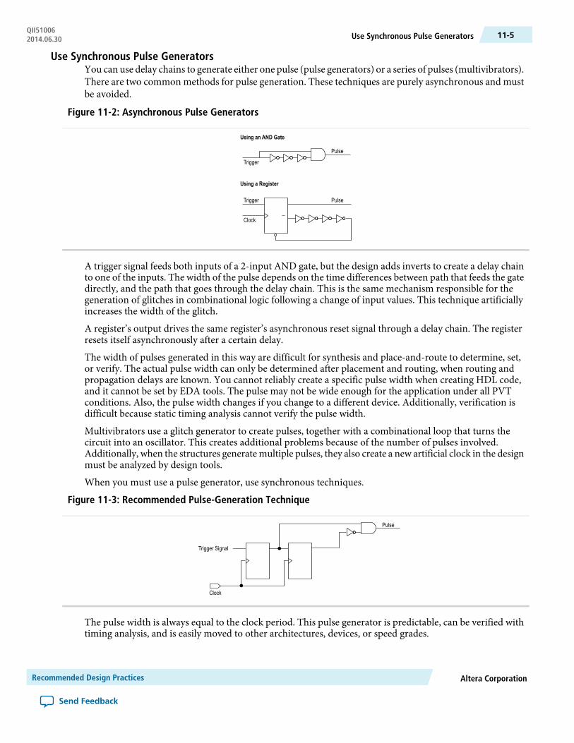
Use Synchronous Pulse GeneratorsYou can use delay chains to generate either one pulse (pulse generators) or a series of pulses (multivibrators).There are two common methods for pulse generation. These techniques are purely asynchronous and mustbe avoided.
Figure 11-2: Asynchronous Pulse Generators
Pulse
PulseTrigger
Trigger
Clock
Using an AND Gate
Using a Register
A trigger signal feeds both inputs of a 2-input AND gate, but the design adds inverts to create a delay chainto one of the inputs. The width of the pulse depends on the time differences between path that feeds the gatedirectly, and the path that goes through the delay chain. This is the same mechanism responsible for thegeneration of glitches in combinational logic following a change of input values. This technique artificiallyincreases the width of the glitch.
A register’s output drives the same register’s asynchronous reset signal through a delay chain. The registerresets itself asynchronously after a certain delay.
The width of pulses generated in this way are difficult for synthesis and place-and-route to determine, set,or verify. The actual pulse width can only be determined after placement and routing, when routing andpropagation delays are known. You cannot reliably create a specific pulse width when creating HDL code,and it cannot be set by EDA tools. The pulse may not be wide enough for the application under all PVTconditions. Also, the pulse width changes if you change to a different device. Additionally, verification isdifficult because static timing analysis cannot verify the pulse width.
Multivibrators use a glitch generator to create pulses, together with a combinational loop that turns thecircuit into an oscillator. This creates additional problems because of the number of pulses involved.Additionally, when the structures generate multiple pulses, they also create a new artificial clock in the designmust be analyzed by design tools.
When you must use a pulse generator, use synchronous techniques.
Figure 11-3: Recommended Pulse-Generation Technique
Trigger Signal
Clock
Pulse
The pulse width is always equal to the clock period. This pulse generator is predictable, can be verified withtiming analysis, and is easily moved to other architectures, devices, or speed grades.
Altera CorporationRecommended Design Practices
Send Feedback
11-5Use Synchronous Pulse GeneratorsQII510062014.06.30

Optimizing Clocking SchemesLike combinational logic, clocking schemes have a large effect on the performance and reliability of a design.
Avoid using internally generated clocks (other than PLLs)wherever possible because they can cause functionaland timing problems in the design. Clocks generated with combinational logic can introduce glitches thatcreate functional problems, and the delay inherent in combinational logic can lead to timing problems.
Specify all clock relationships in the Quartus II software to allow for the best timing-drivenoptimizations during fitting and to allow correct timing analysis. Use clock setting assignments onany derived or internal clocks to specify their relationship to the base clock.
Use global device-wide, low-skew dedicated routing for all internally-generated clocks, instead ofrouting clocks on regular routing lines.
Tip:
Avoid data transfers between different clocks wherever possible. If you require a data transfer betweendifferent clocks, use FIFO circuitry. You can use the clock uncertainty features in the Quartus IIsoftware to compensate for the variable delays between clock domains. Consider setting a clock setupuncertainty and clock hold uncertainty value of 10% to 15% of the clock delay.
The following sections provide specific examples and recommendations for avoiding clocking schemeproblems.
Register Combinational Logic OutputsIf you use the output from combinational logic as a clock signal or as an asynchronous reset signal, you canexpect to see glitches in your design. In a synchronous design, glitches on data inputs of registers are normalevents that have no consequences. However, a glitch or a spike on the clock input (or an asynchronous input)to a register can have significant consequences.
Narrow glitches can violate the register’s minimum pulse width requirements. Setup and hold requirementsmight also be violated if the data input of the register changes when a glitch reaches the clock input. Even ifthe design does not violate timing requirements, the register output can change value unexpectedly andcause functional hazards elsewhere in the design.
To avoid these problems, you should always register the output of combinational logic before you use it asa clock signal.
Figure 11-4: Recommended Clock-Generation Technique
Internally Generated ClockRouted on Global Clock Resource
ClockGeneration
Logic
Registering the output of combinational logic ensures that glitches generated by the combinational logic areblocked at the data input of the register.
Recommended Design PracticesAltera Corporation
Send Feedback
QII51006Optimizing Clocking Schemes11-6 2014.06.30
Avoid Asyncrhonous Clock DivisionDesigns often require clocks that you create by dividing amaster clock.Most Altera FPGAs provide dedicatedphase-locked loop (PLL) circuitry for clock division. Using dedicated PLL circuitry can help you to avoidmany of the problems that can be introduced by asynchronous clock division logic.
When you must use logic to divide a master clock, always use synchronous counters or state machines.Additionally, create your design so that registers always directly generate divided clock signals, and routethe clock on global clock resources. To avoid glitches, do not decode the outputs of a counter or a statemachine to generate clock signals.
Avoid Ripple CountersTo simplify verification, avoid ripple counters in your design. In the past, FPGA designers implementedripple counters to divide clocks by a power of two because the counters are easy to design and may use fewergates than their synchronous counterparts.
Ripple counters use cascaded registers, in which the output pin of one register feeds the clock pin of theregister in the next stage. This cascading can cause problems because the counter creates a ripple clock ateach stage. These ripple clocks must be handled properly during timing analysis, which can be difficult andmay require you to make complicated timing assignments in your synthesis and placement and routingtools.
You can often use ripple clock structures to make ripple counters out of the smallest amount of logic possible.However, in all Altera devices supported by the Quartus II software, using a ripple clock structure to reducethe amount of logic used for a counter is unnecessary because the device allows you to construct a counterusing one logic element per counter bit. You should avoid using ripple counters completely.
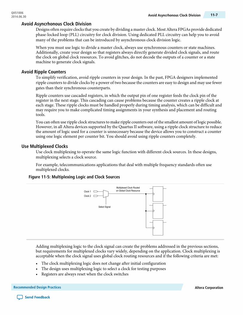
Use Multiplexed ClocksUse clock multiplexing to operate the same logic function with different clock sources. In these designs,multiplexing selects a clock source.
For example, telecommunications applications that deal with multiple frequency standards often usemultiplexed clocks.
Figure 11-5: Multiplexing Logic and Clock Sources
Clock 1Multiplexed Clock Routedon Global Clock Resource
Clock 2
Select Signal
Adding multiplexing logic to the clock signal can create the problems addressed in the previous sections,but requirements for multiplexed clocks vary widely, depending on the application. Clock multiplexing isacceptable when the clock signal uses global clock routing resources and if the following criteria are met:
• The clock multiplexing logic does not change after initial configuration• The design uses multiplexing logic to select a clock for testing purposes• Registers are always reset when the clock switches
Altera CorporationRecommended Design Practices
Send Feedback
11-7Avoid Asyncrhonous Clock DivisionQII510062014.06.30
• A temporarily incorrect response following clock switching has no negative consequences
If the design switches clocks in real timewith no reset signal, and your design cannot tolerate a temporarilyincorrect response, you must use a synchronous design so that there are no timing violations on theregisters, no glitches on clock signals, and no race conditions or other logical problems. By default, theQuartus II software optimizes and analyzes all possible paths through the multiplexer and between bothinternal clocks that may come from the multiplexer. This may lead to more restrictive analysis thanrequired if themultiplexer is always selecting one particular clock. If you do not require themore completeanalysis, you can assign the output of the multiplexer as a base clock in the Quartus II software, so thatall register-to-register paths are analyzed using that clock.
Use dedicated hardware to perform clock multiplexing when it is available, instead of usingmultiplexing logic. For example, you can use the clock-switchover feature or clock control blockavailable in certain Altera devices. These dedicated hardware blocks ensure that you use globallow-skew routing lines and avoid any possible hold time problems on the device due to logic delayon the clock line.
Tip:
For device-specific information about clocking structures, refer to the appropriate device data sheetor handbook on the Literature page of the Altera website.
Note:
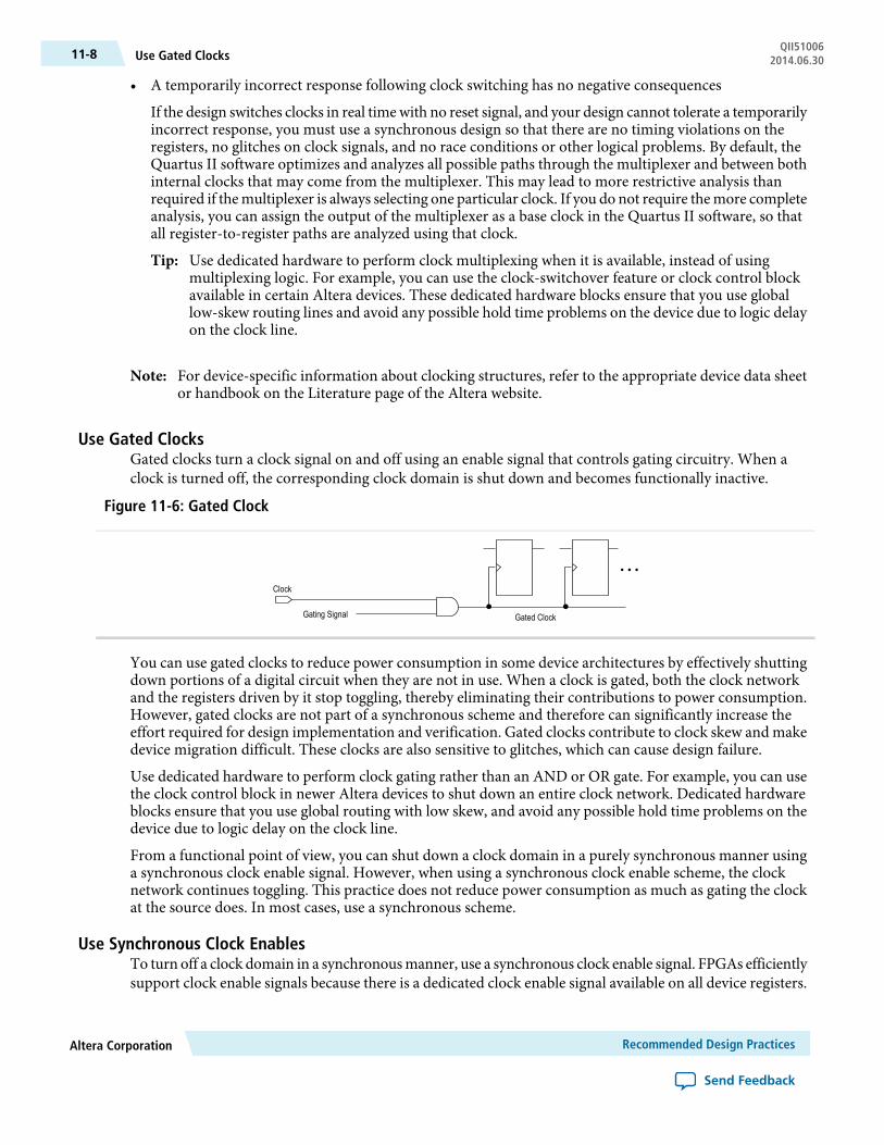
Use Gated ClocksGated clocks turn a clock signal on and off using an enable signal that controls gating circuitry. When aclock is turned off, the corresponding clock domain is shut down and becomes functionally inactive.
Figure 11-6: Gated Clock
Clock
Gated ClockGating Signal
You can use gated clocks to reduce power consumption in some device architectures by effectively shuttingdown portions of a digital circuit when they are not in use. When a clock is gated, both the clock networkand the registers driven by it stop toggling, thereby eliminating their contributions to power consumption.However, gated clocks are not part of a synchronous scheme and therefore can significantly increase theeffort required for design implementation and verification. Gated clocks contribute to clock skew and makedevice migration difficult. These clocks are also sensitive to glitches, which can cause design failure.
Use dedicated hardware to perform clock gating rather than an AND or OR gate. For example, you can usethe clock control block in newer Altera devices to shut down an entire clock network. Dedicated hardwareblocks ensure that you use global routing with low skew, and avoid any possible hold time problems on thedevice due to logic delay on the clock line.
From a functional point of view, you can shut down a clock domain in a purely synchronous manner usinga synchronous clock enable signal. However, when using a synchronous clock enable scheme, the clocknetwork continues toggling. This practice does not reduce power consumption as much as gating the clockat the source does. In most cases, use a synchronous scheme.
Use Synchronous Clock EnablesTo turn off a clock domain in a synchronousmanner, use a synchronous clock enable signal. FPGAs efficientlysupport clock enable signals because there is a dedicated clock enable signal available on all device registers.
Recommended Design PracticesAltera Corporation
Send Feedback
QII51006Use Gated Clocks11-8 2014.06.30
This scheme does not reduce power consumption as much as gating the clock at the source because the clocknetwork keeps toggling, and performs the same function as a gated clock by disabling a set of registers. Inserta multiplexer in front of the data input of every register to either load new data, or copy the output of theregister.
Figure 11-7: Synchronous Clock Enable
Enable
Data
Recommended Clock-Gating MethodsUse gated clocks only when your target application requires power reduction and when gated clocks are ableto provide the required reduction in your device architecture.
If you must use clocks gated by logic, implement these clocks using the robust clock-gating technique andensure that the gated clock signal uses dedicated global clock routing.
You can gate a clock signal at the source of the clock network, at each register, or somewhere in between.Because the clock network contributes to switching power consumption, gate the clock at the sourcewheneverpossible, so that you can shut down the entire clock network instead of gating it further along the clocknetwork at the registers.
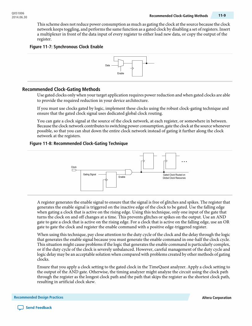
Figure 11-8: Recommended Clock-Gating Technique
Clock
EnableGated Clock Routed onGlobal Clock Resources
Gating Signal
A register generates the enable signal to ensure that the signal is free of glitches and spikes. The register thatgenerates the enable signal is triggered on the inactive edge of the clock to be gated. Use the falling edgewhen gating a clock that is active on the rising edge. Using this technique, only one input of the gate thatturns the clock on and off changes at a time. This prevents glitches or spikes on the output. Use an ANDgate to gate a clock that is active on the rising edge. For a clock that is active on the falling edge, use an ORgate to gate the clock and register the enable command with a positive edge-triggered register.
When using this technique, pay close attention to the duty cycle of the clock and the delay through the logicthat generates the enable signal because you must generate the enable command in one-half the clock cycle.This situation might cause problems if the logic that generates the enable command is particularly complex,or if the duty cycle of the clock is severely unbalanced. However, careful management of the duty cycle andlogic delay may be an acceptable solution when compared with problems created by other methods of gatingclocks.
Ensure that you apply a clock setting to the gated clock in the TimeQuest analyzer. Apply a clock setting tothe output of the AND gate. Otherwise, the timing analyzer might analyze the circuit using the clock paththrough the register as the longest clock path and the path that skips the register as the shortest clock path,resulting in artificial clock skew.
Altera CorporationRecommended Design Practices
Send Feedback
11-9Recommended Clock-Gating MethodsQII510062014.06.30
In certain cases, converting the gated clocks to clock enables may help reduce glitch and clock skew, andeventually produce a more accurate timing analysis. You can set the Quartus II software to automaticallyconvert gated clocks to clock enables by turning on theAutoGatedClockConversion option. The conversionapplies to two types of gated clocking schemes: single-gated clock and cascaded-gated clock.
Optimizing Physical Implementation and Timing ClosureThis section provides design and timing closure techniques for high speed or complex core logic designswith challenging timing requirements. These techniques may also be helpful for low or medium speeddesigns.
Planning Physical ImplementationWhen planning a design, consider the following elements of physical implementation:
• The number of unique clock domains and their relationships• The amount of logic in each functional block• The location and direction of data flow between blocks• How data routes to the functional blocks between I/O interfaces
Interface-wide control or status signals may have competing or opposing constraints. For example, whena functional block's control or status signals interface with physical channels from both sides of the device.In such cases you must provide enough pipeline register stages to allow these signals to traverse the widthof the device. In addition, you can structure the hierarchy of the design into separate logic modules foreach side of the device. The side modules can generate and use registered control signals per side. Thissimplifies floorplanning, particularly in designs with transceivers, by placing per-side logic near thetransceivers.
When adding register stages to pipeline control signals, turn off the Auto Shift Register Replacementoption (Assignments > Settings > Analysis & Synthesis Settings > More Settings) for these registers.By default, chains of registers can be converted to a RAM-based implementation based on performanceand resource estimates. Since pipelining helpsmeet timing requirements over long distance, this assignmentensures that control signals are not converted.
Planning FPGA ResourcesYour design requirements impact the use of FPGA resources. Plan functional blocks with appropriate global,regional, and dual-regional network signals in mind.
In general, after allocating the clocks in a design, use global networks for the highest fan-out control signals.When a global network signal distributes a high fan-out control signal, the global signal can drive logicanywhere in the device. Similarly, when using a regional network signal, the driven must be in one quadrantof the device, or half the device for a dual-regional network signal. Depending on data flow and physicallocations of the data entry and exit between the I/Os and the device, restricting a functional block to aquadrant or half the device may not be practical for performance or resource requirements.
When floorplanning a design, consider the balance of different types of device resources, such as memory,logic, and DSP blocks in the main functional blocks. For example, if a design is memory intensive with asmall amount of logic, it may be difficult to develop an effective floorplan. Logic that interfaces with thememory would have to spread across the chip to access the memory. In this case, it is important to useenough register stages in the data and control paths to allow signals to traverse the chip to access the physicallydisparate resources needed.
Optimizing Timing ClosureYou can make changes to your design and constraints that help you achieve timing closure.
Recommended Design PracticesAltera Corporation
Send Feedback
QII51006Optimizing Physical Implementation and Timing Closure11-10 2014.06.30

Whenever you change the project settings, you must balance any performance improvement of the settingagainst any potential increase in compilation time associatedwith the setting. You can view the performancegain versus runtime cost by reviewing the Fitter messages after design processing.
You can use physical synthesis optimizations for combinational logic, register retiming, and registerduplication techniques to optimize your design for timing closure.
Click Assignments > Settings > Physical Synthesis Optimizations to turn on physical synthesis options.
• Physical synthesis for combinational logic—When the Perform physical synthesis for combinationallogic is turned on, the report panel identifies logic that physical synthesis can modify. You can use thisinformation to modify the design so that the associated optimization can be turned off to save compiletime.
• Register duplication—This technique is most useful where registers have high fan-out, or where the fan-out is in physically distant areas of the device. Review the netlist optimizations report and considermanually duplicating registers automatically added by physical synthesis. You can also locate the originaland duplicate registers in the Chip Planner. Compare their locations, and if the fan-out is improved,modify the code and turn off register duplication to save compile time.
• Register retiming—This technique is particularly useful where some combinatorial paths between registersexceed the timing goal while other paths fall short. If a design is already heavily pipelined, register retimingis less likely to provide significant performance gains since there should not be significantly unbalancedlevels of logic across pipeline stages.
The application of appropriate timing constraints is essential to timing closure. Use the following generalguidelines in applying timing constraints:
• Apply multicycle constraints in your design wherever single-cycle timing analysis is not required.• Apply False Path constraints to all asynchronous clock domain crossings or resets in the design. This
technique prevents overconstraining and the Fitter focuses only on critical paths to reduce compile time.However, over constraining timing critical clock domains can sometimes provide better timing resultsand lower compile times than physical synthesis.
• Overconstrain rather than using physical synthesis when the slack improvement from physical synthesisis near zero. Overconstrain the frequency requirement on timing critical clock domains by using setupuncertainty.
• When evaluating the effect of constraint changes on performance and runtime, compile the design withat least three different seeds to determine the average performance and runtime effects. Different constraintcombinations produce various results. Three samples or more establishes a performance trend. Modifyyour constraints based on performance improvement or decline.
• Leave settings at the default value whenever possible. Increasing performance constraints can increasethe compile time significantly. While those increases may be necessary to close timing on a design, usingthe default settings whenever possible minimizes compile time.
Optimizing Critical Timing PathsTo close timing in high speed designs, review paths with the largest timing failures. Correcting a single, largetiming failure can result in a very significant timing improvement.
Review the register placement and routing paths by clicking Tools > Chip Planner. Large timing failureson high fan-out control signals can be caused by any of the following conditions:
• Sub-optimal use of global networks• Signals that traverse the chip on local routing without pipelining
Altera CorporationRecommended Design Practices
Send Feedback
11-11Optimizing Critical Timing PathsQII510062014.06.30
• Failure to correct high fan-out by register duplication
For high-speed and high-bandwidth designs, optimize speed by reducing bus width and wire usage. Toreduce wire use, move the data as little as possible. For example, if a block of logic functions on a few bitsof a word, store inactive bits in a fifo ormemory.Memory is cheaper and denser than registers and reduceswire usage.
Optimizing Power ConsumptionThe total FPGA power consumption is comprised of I/O power, core static power, and core dynamic power.Knowledge of the relationship between these components is fundamental in calculating the overall totalpower consumption.
You can use various optimization techniques and tools tominimize power consumptionwhen applied duringFPGA design implementation. The Quartus II software offers power-driven compilation features to fullyoptimize device power consumption. Power-driven compilation focuses on reducing your design’s totalpower consumption using power-driven synthesis and power-driven placement and routing.
Managing Design MetastabilityMetastability in PLD designs can be caused by the synchronization of asynchronous signals. You can usethe Quartus II software to analyze the mean time between failures (MTBF) due to metastability, thusoptimizing the design to improve the metastability MTBF. A high metastability MTBF indicates a morerobust design.
Related InformationViewing Metastability ReportsFormore information about viewingmetastability reports, refer to ViewingMetastability Reports inQuartusII Help.
Checking Design ViolationsTo improve the reliability, timing performance, and logic utilization of your design, avoid design ruleviolations. The Quartus II software provides the Design Assistant tool that automatically checks for designrule violations and reports their location.
The Design Assistant is a design rule checking tool that allows you to check for design issues early in thedesign flow. TheDesignAssistant checks your design for adherence toAltera-recommendeddesign guidelines.You can specify which rules you want the Design Assistant to apply to your design. This is useful if you knowthat your design violates particular rules that are not critical and you can allow these rule violations. TheDesign Assistant generates design violation reports with details about each violation based on the settingsthat you specified.
This section provides an introduction to the Quartus II design flow with the Design Assistant, messageseverity levels, and an explanation about how to set up the Design Assistant. The last parts of the sectiondescribe the design rules and the reports generated by the Design Assistant. The Design Assistant supportsall Altera devices supported by the Quartus II software.
Validating Against Design RulesYou can run the Design Assistant following design synthesis or compilation. The Design Assistant performsa post-fit netlist analysis of your design.
Recommended Design PracticesAltera Corporation
Send Feedback
QII51006Optimizing Power Consumption11-12 2014.06.30
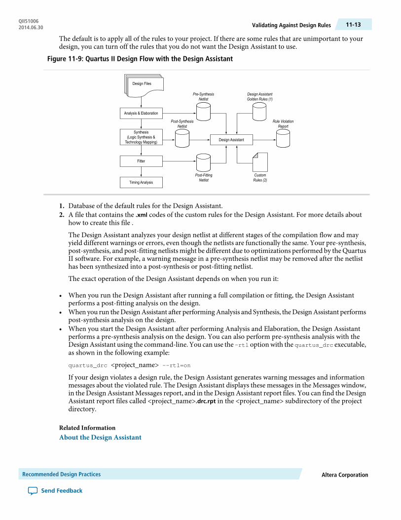
The default is to apply all of the rules to your project. If there are some rules that are unimportant to yourdesign, you can turn off the rules that you do not want the Design Assistant to use.
Figure 11-9: Quartus II Design Flow with the Design Assistant
Design Files
Analysis & Elaboration
Synthesis(Logic Synthesis &
Technology Mapping)
Fitter
Timing Analysis
Design Assistant
Pre-SynthesisNetlist
Design AssistantGolden Rules (1)
Rule ViolationReport
CustomRules (2)
Post-FittingNetlist
Post-SynthesisNetlist
1. Database of the default rules for the Design Assistant.2. A file that contains the .xml codes of the custom rules for the Design Assistant. For more details about
how to create this file .
The Design Assistant analyzes your design netlist at different stages of the compilation flow and mayyield different warnings or errors, even though the netlists are functionally the same. Your pre-synthesis,post-synthesis, and post-fitting netlists might be different due to optimizations performed by the QuartusII software. For example, a warning message in a pre-synthesis netlist may be removed after the netlisthas been synthesized into a post-synthesis or post-fitting netlist.
The exact operation of the Design Assistant depends on when you run it:
• When you run the Design Assistant after running a full compilation or fitting, the Design Assistantperforms a post-fitting analysis on the design.
• When you run theDesignAssistant after performingAnalysis and Synthesis, theDesignAssistant performspost-synthesis analysis on the design.
• When you start the Design Assistant after performing Analysis and Elaboration, the Design Assistantperforms a pre-synthesis analysis on the design. You can also perform pre-synthesis analysis with theDesignAssistant using the command-line. You can use the -rtl optionwith the quartus_drc executable,as shown in the following example:
quartus_drc <project_name> --rtl=on
If your design violates a design rule, the Design Assistant generates warning messages and informationmessages about the violated rule. The Design Assistant displays these messages in the Messages window,in the Design Assistant Messages report, and in the Design Assistant report files. You can find the DesignAssistant report files called <project_name>.drc.rpt in the <project_name> subdirectory of the projectdirectory.
Related InformationAbout the Design Assistant
Altera CorporationRecommended Design Practices
Send Feedback
11-13Validating Against Design RulesQII510062014.06.30
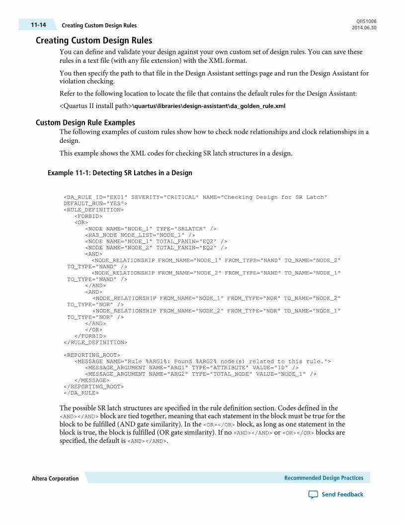
Creating Custom Design RulesYou can define and validate your design against your own custom set of design rules. You can save theserules in a text file (with any file extension) with the XML format.
You then specify the path to that file in the Design Assistant settings page and run the Design Assistant forviolation checking.
Refer to the following location to locate the file that contains the default rules for the Design Assistant:
<Quartus II install path>\quartus\libraries\design-assistant\da_golden_rule.xml
Custom Design Rule ExamplesThe following examples of custom rules show how to check node relationships and clock relationships in adesign.
This example shows the XML codes for checking SR latch structures in a design.
Example 11-1: Detecting SR Latches in a Design
<DA_RULE ID="EX01" SEVERITY="CRITICAL" NAME="Checking Design for SR Latch" DEFAULT_RUN="YES"><RULE_DEFINITION> <FORBID> <OR> <NODE NAME="NODE_1" TYPE="SRLATCH" /> <HAS_NODE NODE_LIST="NODE_1" /> <NODE NAME="NODE_1" TOTAL_FANIN="EQ2" /> <NODE NAME="NODE_2" TOTAL_FANIN="EQ2" /> <AND> <NODE_RELATIONSHIP FROM_NAME="NODE_1" FROM_TYPE="NAND" TO_NAME="NODE_2" TO_TYPE="NAND" /> <NODE_RELATIONSHIP FROM_NAME="NODE_2" FROM_TYPE="NAND" TO_NAME="NODE_1" TO_TYPE="NAND" /> </AND> <AND> <NODE_RELATIONSHIP FROM_NAME="NODE_1" FROM_TYPE="NOR" TO_NAME="NODE_2" TO_TYPE="NOR" /> <NODE_RELATIONSHIP FROM_NAME="NODE_2" FROM_TYPE="NOR" TO_NAME="NODE_1" TO_TYPE="NOR" /> </AND> </OR> </FORBID></RULE_DEFINITION>
<REPORTING_ROOT> <MESSAGE NAME="Rule %ARG1%: Found %ARG2% node(s) related to this rule."> <MESSAGE_ARGUMENT NAME="ARG1" TYPE="ATTRIBUTE" VALUE="ID" /> <MESSAGE_ARGUMENT NAME="ARG2" TYPE="TOTAL_NODE" VALUE="NODE_1" /> </MESSAGE></REPORTING_ROOT></DA_RULE>
The possible SR latch structures are specified in the rule definition section. Codes defined in the<AND></AND> block are tied together, meaning that each statement in the block must be true for theblock to be fulfilled (AND gate similarity). In the <OR></OR> block, as long as one statement in theblock is true, the block is fulfilled (OR gate similarity). If no <AND></AND> or <OR></OR> blocks arespecified, the default is <AND></AND>.
Recommended Design PracticesAltera Corporation
Send Feedback
QII51006Creating Custom Design Rules11-14 2014.06.30
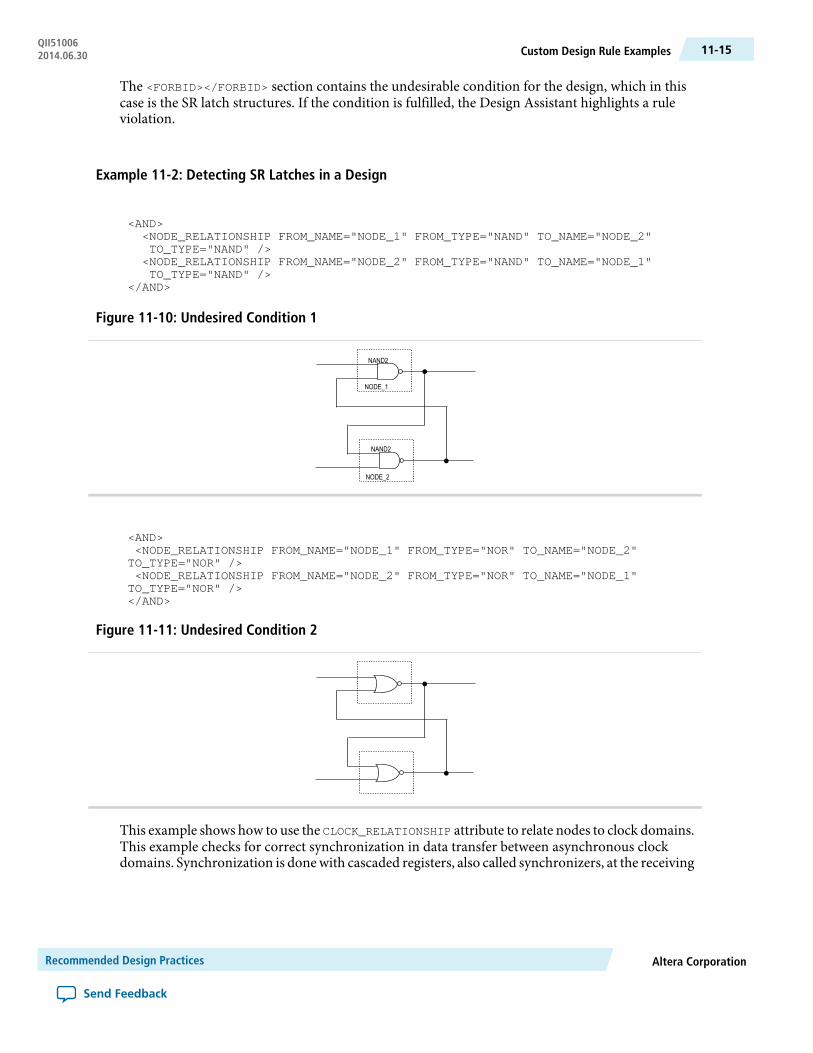
The <FORBID></FORBID> section contains the undesirable condition for the design, which in thiscase is the SR latch structures. If the condition is fulfilled, the Design Assistant highlights a ruleviolation.
Example 11-2: Detecting SR Latches in a Design
<AND> <NODE_RELATIONSHIP FROM_NAME="NODE_1" FROM_TYPE="NAND" TO_NAME="NODE_2" TO_TYPE="NAND" /> <NODE_RELATIONSHIP FROM_NAME="NODE_2" FROM_TYPE="NAND" TO_NAME="NODE_1" TO_TYPE="NAND" /></AND>
Figure 11-10: Undesired Condition 1
NAND2
NODE_1
NAND2
NODE_2
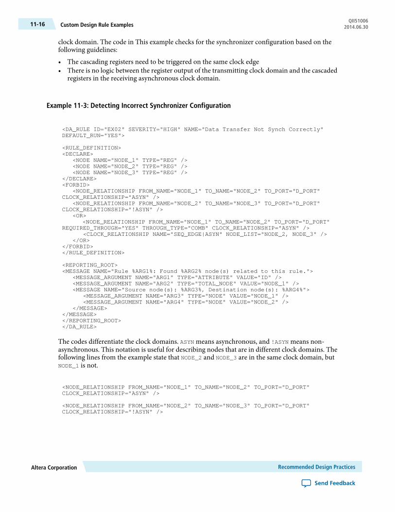
<AND> <NODE_RELATIONSHIP FROM_NAME="NODE_1" FROM_TYPE="NOR" TO_NAME="NODE_2" TO_TYPE="NOR" /> <NODE_RELATIONSHIP FROM_NAME="NODE_2" FROM_TYPE="NOR" TO_NAME="NODE_1" TO_TYPE="NOR" /></AND>
Figure 11-11: Undesired Condition 2
This example shows how to use the CLOCK_RELATIONSHIP attribute to relate nodes to clock domains.This example checks for correct synchronization in data transfer between asynchronous clockdomains. Synchronization is donewith cascaded registers, also called synchronizers, at the receiving
Altera CorporationRecommended Design Practices
Send Feedback
11-15Custom Design Rule ExamplesQII510062014.06.30
clock domain. The code in This example checks for the synchronizer configuration based on thefollowing guidelines:
• The cascading registers need to be triggered on the same clock edge• There is no logic between the register output of the transmitting clock domain and the cascaded
registers in the receiving asynchronous clock domain.
Example 11-3: Detecting Incorrect Synchronizer Configuration
<DA_RULE ID="EX02" SEVERITY="HIGH" NAME="Data Transfer Not Synch Correctly" DEFAULT_RUN="YES">
<RULE_DEFINITION><DECLARE> <NODE NAME="NODE_1" TYPE="REG" /> <NODE NAME="NODE_2" TYPE="REG" /> <NODE NAME="NODE_3" TYPE="REG" /> </DECLARE><FORBID> <NODE_RELATIONSHIP FROM_NAME="NODE_1" TO_NAME="NODE_2" TO_PORT="D_PORT" CLOCK_RELATIONSHIP="ASYN" /> <NODE_RELATIONSHIP FROM_NAME="NODE_2" TO_NAME="NODE_3" TO_PORT="D_PORT" CLOCK_RELATIONSHIP="!ASYN" /> <OR> <NODE_RELATIONSHIP FROM_NAME="NODE_1" TO_NAME="NODE_2" TO_PORT="D_PORT" REQUIRED_THROUGH="YES" THROUGH_TYPE="COMB" CLOCK_RELATIONSHIP="ASYN" /> <CLOCK_RELATIONSHIP NAME="SEQ_EDGE|ASYN" NODE_LIST="NODE_2, NODE_3" /> </OR></FORBID></RULE_DEFINITION>
<REPORTING_ROOT><MESSAGE NAME="Rule %ARG1%: Found %ARG2% node(s) related to this rule."> <MESSAGE_ARGUMENT NAME="ARG1" TYPE="ATTRIBUTE" VALUE="ID" /> <MESSAGE_ARGUMENT NAME="ARG2" TYPE="TOTAL_NODE" VALUE="NODE_1" /> <MESSAGE NAME="Source node(s): %ARG3%, Destination node(s): %ARG4%"> <MESSAGE_ARGUMENT NAME="ARG3" TYPE="NODE" VALUE="NODE_1" /> <MESSAGE_ARGUMENT NAME="ARG4" TYPE="NODE" VALUE="NODE_2" /> </MESSAGE></MESSAGE></REPORTING_ROOT></DA_RULE>
The codes differentiate the clock domains. ASYN means asynchronous, and !ASYN means non-asynchronous. This notation is useful for describing nodes that are in different clock domains. Thefollowing lines from the example state that NODE_2 and NODE_3 are in the same clock domain, butNODE_1 is not.
<NODE_RELATIONSHIP FROM_NAME="NODE_1" TO_NAME="NODE_2" TO_PORT="D_PORT" CLOCK_RELATIONSHIP="ASYN" />
<NODE_RELATIONSHIP FROM_NAME="NODE_2" TO_NAME="NODE_3" TO_PORT="D_PORT" CLOCK_RELATIONSHIP="!ASYN" />
Recommended Design PracticesAltera Corporation
Send Feedback
QII51006Custom Design Rule Examples11-16 2014.06.30
The next line of code states that NODE_2 and NODE_3 have a clock relationship of either sequentialedge or asynchronous.
<CLOCK_RELATIONSHIP NAME="SEQ_EDGE|ASYN" NODE_LIST="NODE_2, NODE_3" />
The <FORBID></FORBID> section contains the undesirable condition for the design, which in thiscase is the undesired configuration of the synchronizer. If the condition is fulfilled, the DesignAssistant highlights a rule violation.
The possible SR latch structures are specified in the rule definition section. Codes defined in the<AND></AND> block are tied together, meaning that each statement in the block must be true for theblock to be fulfilled (AND gate similarity). In the <OR></OR> block, as long as one statement in theblock is true, the block is fulfilled (OR gate similarity). If no <AND></AND> or <OR></OR> blocks arespecified, the default is <AND></AND>.
The <FORBID></FORBID> section contains the undesirable condition for the design, which in thiscase is the SR latch structures. If the condition is fulfilled, the Design Assistant highlights a ruleviolation.
The following examples show the undesired conditions from with their equivalent block diagrams:
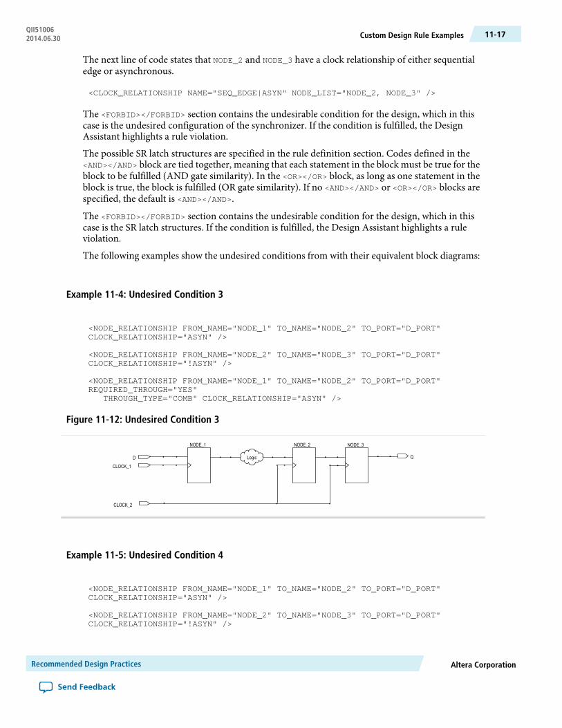
Example 11-4: Undesired Condition 3
<NODE_RELATIONSHIP FROM_NAME="NODE_1" TO_NAME="NODE_2" TO_PORT="D_PORT" CLOCK_RELATIONSHIP="ASYN" />
<NODE_RELATIONSHIP FROM_NAME="NODE_2" TO_NAME="NODE_3" TO_PORT="D_PORT" CLOCK_RELATIONSHIP="!ASYN" />
<NODE_RELATIONSHIP FROM_NAME="NODE_1" TO_NAME="NODE_2" TO_PORT="D_PORT" REQUIRED_THROUGH="YES" THROUGH_TYPE="COMB" CLOCK_RELATIONSHIP="ASYN" />
Figure 11-12: Undesired Condition 3
NODE_1
Logic
NODE_2 NODE_3
DCLOCK_1
CLOCK_2
Q
Example 11-5: Undesired Condition 4
<NODE_RELATIONSHIP FROM_NAME="NODE_1" TO_NAME="NODE_2" TO_PORT="D_PORT" CLOCK_RELATIONSHIP="ASYN" />
<NODE_RELATIONSHIP FROM_NAME="NODE_2" TO_NAME="NODE_3" TO_PORT="D_PORT" CLOCK_RELATIONSHIP="!ASYN" />
Altera CorporationRecommended Design Practices
Send Feedback
11-17Custom Design Rule ExamplesQII510062014.06.30
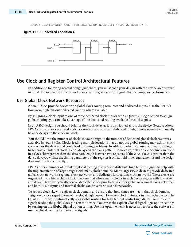
<CLOCK_RELATIONSHIP NAME="SEQ_EDGE|ASYN" NODE_LIST="NODE_2, NODE_3" />
Figure 11-13: Undesired Condition 4
NODE_1 NODE_2 NODE_3
DCLOCK_1
CLOCK_2
Q
Use Clock and Register-Control Architectural FeaturesIn addition to following general design guidelines, you must code your design with the device architecturein mind. FPGAs provide device-wide clocks and register control signals that can improve performance.
Use Global Clock Network ResourcesAltera FPGAs provide device-wide global clock routing resources and dedicated inputs. Use the FPGA’slow-skew, high fan-out dedicated routing where available.
By assigning a clock input to one of these dedicated clock pins or with a Quartus II logic option to assignglobal routing, you can take advantage of the dedicated routing available for clock signals.
In an ASIC design, you should balance the clock delay as it is distributed across the device. Because AlteraFPGAs provide device-wide global clock routing resources and dedicated inputs, there is no need tomanuallybalance delays on the clock network.
You should limit the number of clocks in your design to the number of dedicated global clock resourcesavailable in your FPGA. Clocks feeding multiple locations that do not use global routing may exhibit clockskew across the device that could lead to timing problems. In addition, when you use combinational logicto generate an internal clock, it adds delays on the clock path. In some cases, delay on a clock line can resultin a clock skew greater than the data path length between two registers. If the clock skew is greater than thedata delay, you violate the timing parameters of the register (such as hold time requirements) and the designdoes not function correctly.
FPGAs offer a number of low-skew global routing resources to distribute high fan-out signals to help withthe implementation of large designs with many clock domains. Many large FPGA devices provide dedicatedglobal clock networks, regional clock networks, and dedicated fast regional clock networks. These clocks areorganized into a hierarchical clock structure that allows many clocks in each device region with low skewand delay. There are typically several dedicated clock pins to drive either global or regional clock networks,and both PLL outputs and internal clocks can drive various clock networks.
To reduce clock skew in a given clock domain and ensure that hold times are met in that clock domain,assign each clock signal to one of the global high fan-out, low-skew clock networks in the FPGA device. TheQuartus II software automatically uses global routing for high fan-out control signals, PLL outputs, andsignals feeding the global clock pins on the device. You can make explicit Global Signal logic option settingsby turning on the Global Signal option setting. Use this option when it is necessary to force the software touse the global routing for particular signals.
Recommended Design PracticesAltera Corporation
Send Feedback
QII51006Use Clock and Register-Control Architectural Features11-18 2014.06.30

To take full advantage of these routing resources, the sources of clock signals in a design (input clock pinsor internally-generated clocks) need to drive only the clock input ports of registers. In older Altera devicefamilies, if a clock signal feeds the data ports of a register, the signal may not be able to use dedicated routing,which can lead to decreased performance and clock skew problems. In general, allowing clock signals todrive the data ports of registers is not considered synchronous design and can complicate timing analysis.
Use Global Reset ResourcesASIC designs may use local resets to avoid long routing delays. Take advantage of the device-wideasynchronous reset pin available on most FPGAs to eliminate these problems. This reset signal provideslow-skew routing across the device.
The following are three types of resets used in synchronous circuits:
• Synchronous Reset• Asynchronous Reset• Synchronized Asynchronous Reset—preferred when designing an FPGA circuit
Use Synchronous ResetsThe synchronous reset ensures that the circuit is fully synchronous. You can easily time the circuit with theQuartus II TimeQuest analyzer.
Because clocks that are synchronous to each other launch and latch the reset signal, the data arrival and datarequired times are easily determined for proper slack analysis. The synchronous reset is easier to use withcycle-based simulators.
There are two methods by which a reset signal can reach a register; either by being gated in with the datainput, or by using an LAB-wide control signal (synclr). If you use the first method, you risk adding anadditional gate delay to the circuit to accommodate the reset signal, which causes increased data arrival timesand negatively impacts setup slack. The second method relies on dedicated routing in the LAB to eachregister, but this is slower than an asynchronous reset to the same register.
Figure 11-14: Synchronous Reset
DFFAND2
inst1
Altera CorporationRecommended Design Practices
Send Feedback
11-19Use Global Reset ResourcesQII510062014.06.30
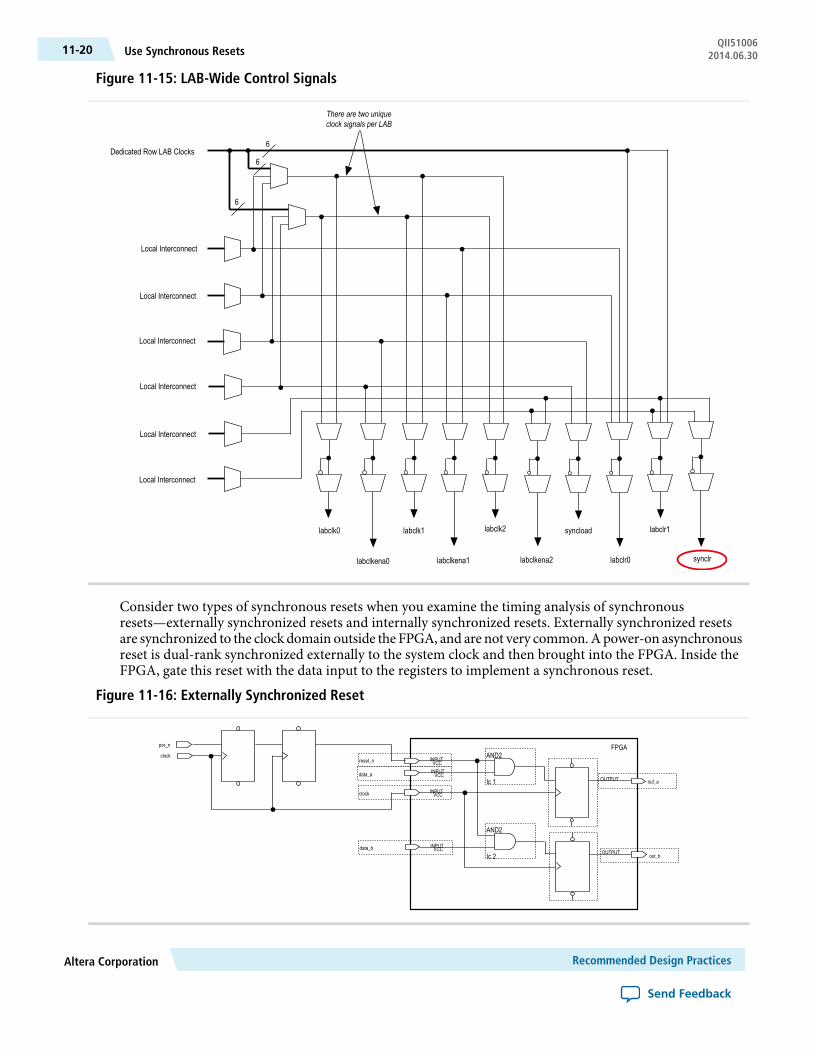
Figure 11-15: LAB-Wide Control Signals
Dedicated Row LAB Clocks
Local Interconnect
Local Interconnect
Local Interconnect
Local Interconnect
Local Interconnect
Local Interconnect
There are two uniqueclock signals per LAB
6
6
6
labclk0
labclkena0
labclk1 labclk2 syncload labclr1
labclkena1 labclkena2 labclr0 synclr
Consider two types of synchronous resets when you examine the timing analysis of synchronousresets—externally synchronized resets and internally synchronized resets. Externally synchronized resetsare synchronized to the clock domain outside the FPGA, and are not very common.Apower-on asynchronousreset is dual-rank synchronized externally to the system clock and then brought into the FPGA. Inside theFPGA, gate this reset with the data input to the registers to implement a synchronous reset.
Figure 11-16: Externally Synchronized Reset
por_n
clockreset_n
data_a
INPUTVCC
VCCINPUT
VCCINPUTclock
VCCINPUTdata_b
AND2
lc 1
AND2
lc 2
OUTPUT out_a
out_bOUTPUT
FPGA
Recommended Design PracticesAltera Corporation
Send Feedback
QII51006Use Synchronous Resets11-20 2014.06.30
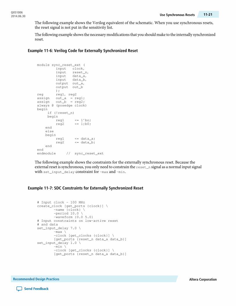
The following example shows the Verilog equivalent of the schematic. When you use synchronous resets,the reset signal is not put in the sensitivity list.
The following example shows the necessarymodifications that you shouldmake to the internally synchronizedreset.
Example 11-6: Verilog Code for Externally Synchronized Reset
module sync_reset_ext ( input clock, input reset_n, input data_a, input data_b, output out_a, output out_b );reg reg1, reg2assign out_a = reg1;assign out_b = reg2;always @ (posedge clock)begin if (!reset_n) begin reg1 <= 1’bo; reg2 <= 1;b0; end else begin reg1 <= data_a; reg2 <= data_b; endendendmodule // sync_reset_ext
The following example shows the constraints for the externally synchronous reset. Because theexternal reset is synchronous, you only need to constrain the reset_n signal as a normal input signalwith set_input_delay constraint for -max and -min.
Example 11-7: SDC Constraints for Externally Synchronized Reset
# Input clock - 100 MHzcreate_clock [get_ports {clock}] \ -name {clock} \ -period 10.0 \ -waveform {0.0 5.0}# Input constraints on low-active reset# and dataset_input_delay 7.0 \ -max \ -clock [get_clocks {clock}] \ [get_ports {reset_n data_a data_b}]set_input_delay 1.0 \ -min \ -clock [get_clocks {clock}] \ [get_ports {reset_n data_a data_b}]
Altera CorporationRecommended Design Practices
Send Feedback
11-21Use Synchronous ResetsQII510062014.06.30
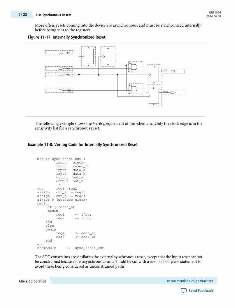
More often, resets coming into the device are asynchronous, and must be synchronized internallybefore being sent to the registers.
Figure 11-17: Internally Synchronized Reset
INPUTVCC
VCCINPUT
VCCINPUT
VCCINPUT
AND2
lc 1
AND2
lc 2
OUTPUT
OUTPUT
The following example shows the Verilog equivalent of the schematic. Only the clock edge is in thesensitivity list for a synchronous reset.
Example 11-8: Verilog Code for Internally Synchronized Reset
module sync_reset_ext ( input clock, input reset_n, input data_a, input data_b, output out_a, output out_b );reg reg1, reg2assign out_a = reg1;assign out_b = reg2;always @ (posedge clock)begin if (!reset_n) begin reg1 <= 1’bo; reg2 <= 1;b0; end else begin reg1 <= data_a; reg2 <= data_b; endendendmodule // sync_reset_ext
The SDC constraints are similar to the external synchronous reset, except that the input reset cannotbe constrained because it is asynchronous and should be cut with a set_false_path statement toavoid these being considered as unconstrained paths.
Recommended Design PracticesAltera Corporation
Send Feedback
QII51006Use Synchronous Resets11-22 2014.06.30
Example 11-9: SDC Constraints for Internally Synchronized Reset
# Input clock - 100 MHzcreate_clock [get_ports {clock}] \ -name {clock} \ -period 10.0 \ -waveform {0.0 5.0}# Input constraints on dataset_input_delay 7.0 \ -max \ -clock [get_clocks {clock}] \ [get_ports {data_a data_b}]set_input_delay 1.0 \ -min \ -clock [get_clocks {clock}] \ [get_ports {data_a data_b}]# Cut the asynchronous reset inputset_false_path \ -from [get_ports {reset_n}] \ -to [all_registers]
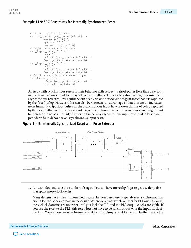
An issue with synchronous resets is their behavior with respect to short pulses (less than a period)on the asynchronous input to the synchronizer flipflops. This can be a disadvantage because theasynchronous reset requires a pulse width of at least one period wide to guarantee that it is capturedby the first flipflop. However, this can also be viewed as an advantage in that this circuit increasesnoise immunity. Spurious pulses on the asynchronous input have a lower chance of being capturedby the first flipflop, so the pulses do not trigger a synchronous reset. In some cases, you might wantto increase the noise immunity further and reject any asynchronous input reset that is less than n
periods wide to debounce an asynchronous input reset.
Figure 11-18: Internally Synchronized Reset with Pulse Extender
INPUTVCC
VCCINPUT
VCCINPUT
VCCINPUT
AND2
lc 1
AND2
lc 2
OUTPUT
OUTPUT
BNAND2
Synchronizer Flip-Flops n Pulse Extender Flip-Flops
lc 3
1. Junction dots indicate the number of stages. You can have more flip flops to get a wider pulsethat spans more clock cycles.
Many designs havemore than one clock signal. In these cases, use a separate reset synchronizationcircuit for each clock domain in the design.When you create synchronizers for PLL output clocks,these clock domains are not reset until you lock the PLL and the PLL output clocks are stable. Ifyou use the reset to the PLL, this reset does not have to be synchronous with the input clock ofthe PLL. You can use an asynchronous reset for this. Using a reset to the PLL further delays the
Altera CorporationRecommended Design Practices
Send Feedback
11-23Use Synchronous ResetsQII510062014.06.30
assertion of a synchronous reset to the PLL output clock domains when using internallysynchronized resets.
Using Asynchronous ResetsAsynchronous resets are themost common formof reset in circuit designs, as well as the easiest to implement.Typically, you can insert the asynchronous reset into the device, turn on the global buffer, and connect tothe asynchronous reset pin of every register in the device.
Thismethod is only advantageous under certain circumstances—you do not need to always reset the register.Unlike the synchronous reset, the asynchronous reset is not inserted in the data path, and does not negativelyimpact the data arrival times between registers. Reset takes effect immediately, and as soon as the registersreceive the reset pulse, the registers are reset. The asynchronous reset is not dependent on the clock.
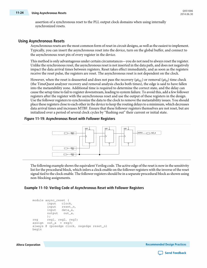
However, when the reset is deasserted and does not pass the recovery (µtSU) or removal (µtH) time check(the TimeQuest analyzer recovery and removal analysis checks both times), the edge is said to have falleninto the metastability zone. Additional time is required to determine the correct state, and the delay cancause the setup time to fail to register downstream, leading to system failure. To avoid this, add a few followerregisters after the register with the asynchronous reset and use the output of these registers in the design.Use the follower registers to synchronize the data to the clock to remove the metastability issues. You shouldplace these registers close to each other in the device to keep the routing delays to aminimum,which decreasesdata arrival times and increases MTBF. Ensure that these follower registers themselves are not reset, but areinitialized over a period of several clock cycles by “flushing out” their current or initial state.
Figure 11-19: Asynchronous Reset with Follower Registers
DFF DFF DFF
INPUTVCC
VCCINPUT
VCCINPUT
out_aOUTPUT
The following example shows the equivalent Verilog code. The active edge of the reset is now in the sensitivitylist for the procedural block, which infers a clock enable on the follower registers with the inverse of the resetsignal tied to the clock enable. The follower registers should be in a separate procedural block as shown usingnon-blocking assignments.
Example 11-10: Verilog Code of Asynchronous Reset with Follower Registers
module async_reset ( input clock, input reset_n, input data_a, output out_a, );reg reg1, reg2, reg3;assign out_a = reg3;always @ (posedge clock, negedge reset_n)begin
Recommended Design PracticesAltera Corporation
Send Feedback
QII51006Using Asynchronous Resets11-24 2014.06.30

if (!reset_n) reg1 <= 1’b0; else reg1 <= data_a;endalways @ (posedge clock)begin reg2 <= reg1; reg3 <= reg2;endendmodule // async_reset
You can easily constrain an asynchronous reset. By definition, asynchronous resets have a non-deterministic relationship to the clock domains of the registers they are resetting. Therefore, statictiming analysis of these resets is not possible and you can use the set_false_path command toexclude the path from timing analysis. Because the relationship of the reset to the clock at the registeris not known, you cannot run recovery and removal analysis in the TimeQuest analyzer for thispath. Attempting to do so even without the false path statement results in no paths reported forrecovery and removal.
Example 11-11: SDC Constraints for Asynchronous Reset
# Input clock - 100 MHzcreate_clock [get_ports {clock}] \ -name {clock} \ -period 10.0 \ -waveform {0.0 5.0}# Input constraints on dataset_input_delay 7.0 \ -max \ -clock [get_clocks {clock}]\ [get_ports {data_a}]set_input_delay 1.0 \ -min \ -clock [get_clocks {clock}] \ [get_ports {data_a}]# Cut the asynchronous reset inputset_false_path \ -from [get_ports {reset_n}] \ -to [all_registers]
The asynchronous reset is susceptible to noise, and a noisy asynchronous reset can cause a spuriousreset. You must ensure that the asynchronous reset is debounced and filtered. You can easily enterinto a reset asynchronously, but releasing a reset asynchronously can lead to potential problems(also referred to as “reset removal”) withmetastability, including the hazards of unwanted situationswith synchronous circuits involving feedback.
Use Synchronized Asynchronous ResetTo avoid potential problems associated with purely synchronous resets and purely asynchronous resets, youcan use synchronized asynchronous resets. Synchronized asynchronous resets combine the advantages ofsynchronous and asynchronous resets.
These resets are asynchronously asserted and synchronously deasserted. This takes effect almost instanta-neously, and ensures that no data path for speed is involved, and that the circuit is synchronous for timinganalysis and is resistant to noise.
Altera CorporationRecommended Design Practices
Send Feedback
11-25Use Synchronized Asynchronous ResetQII510062014.06.30

The following example shows amethod for implementing the synchronized asynchronous reset. You shoulduse synchronizer registers in a similar manner as synchronous resets. However, the asynchronous reset inputis gated directly to the CLRN pin of the synchronizer registers and immediately asserts the resulting reset.When the reset is deasserted, logic “1” is clocked through the synchronizers to synchronously deassert theresulting reset.
Figure 11-20: Schematic of Synchronized Asynchronous Reset
DFF
reg3
VCC
DFF
reg4
DFF
reg1
DFF
reg2
data_a
clock
INPUTVCC
VCCINPUT
VCCINPUTreset_n
VCCINPUTdata_b
out_aOUTPUT
out_bOUTPUT
The following example shows the equivalent Verilog HDL code. Use the active edge of the reset in thesensitivity list for the blocks.
Example 11-12: Verilog Code for Synchronized Asynchronous Reset
module sync_async_reset ( input clock, input reset_n, input data_a, input data_b, output out_a, output out_b );reg reg1, reg2;reg reg3, reg4;assign out_a = reg1;assign out_b = reg2;assign rst_n = reg4;always @ (posedge clock, negedge reset_n)begin if (!reset_n) begin reg3 <= 1’b0; reg4 <= 1;b0; end else begin reg3 <= 1’b1; reg4 <= reg3; endend
Recommended Design PracticesAltera Corporation
Send Feedback
QII51006Use Synchronized Asynchronous Reset11-26 2014.06.30

always @ (posedge clock, negedge rst_n)begin if (!rst_n) begin reg1 <= 1’b0; reg2 <= 1;b0; end else begin reg1 <= data_a; reg2 <= data_b; endendendmodule // sync_async_reset
To minimize the metastability effect between the two synchronization registers, and to increase theMTBF, the registers should be located as close as possible in the device to minimize routing delay.If possible, locate the registers in the same logic array block (LAB). The input reset signal (reset_n)must be excluded with a set_false_path command:
set_false_path -from [get_ports {reset_n}] -to [all_registers]
The set_false_path command used with the specified constraint excludes unnecessary inputtiming reports that would otherwise result from specifying an input delay on the reset pin.
The instantaneous assertion of synchronized asynchronous resets is susceptible to noise and runtpulses. If possible, you should debounce the asynchronous reset and filter the reset before it entersthe device. The circuit ensures that the synchronized asynchronous reset is at least one full clockperiod in length. To extend this time to n clock periods, youmust increase the number of synchronizerregisters to n + 1. You must connect the asynchronous input reset (reset_n) to the CLRN pin of allthe synchronizer registers tomaintain the asynchronous assertion of the synchronized asynchronousreset.
Avoid Asynchronous Register Control SignalsAvoid using an asynchronous load signal if the design target device architecture does not include registerswith dedicated circuitry for asynchronous loads. Also, avoid using both asynchronous clear and preset if thearchitecture provides only one of these control signals.
Some Altera devices directly support an asynchronous clear function, but not a preset or load function.When the target device does not directly support the signals, the synthesis or placement and routing softwaremust use combinational logic to implement the same functionality. In addition, if you use signals in a priorityother than the inherent priority in the device architecture, combinational logicmay be required to implementthe necessary control signals. Combinational logic is less efficient and can cause glitches and other problems;it is best to avoid these implementations.
Implementing Embedded RAMAltera’s dedicated memory architecture offers many advanced features that you can enable withAltera-provided IP cores. Use synchronousmemory blocks for your design, so that the blocks can bemappeddirectly into the device dedicated memory blocks.
You can use single-port, dual-port, or three-port RAM with a single- or dual-clocking method. You shouldnot infer the asynchronous memory logic as a memory block or place the asynchronous memory logic inthe dedicated memory block, but implement the asynchronous memory logic in regular logic cells.
Altera CorporationRecommended Design Practices
Send Feedback
11-27Avoid Asynchronous Register Control SignalsQII510062014.06.30
Altera memory blocks have different read-during-write behaviors, depending on the targeted device family,memory mode, and block type. Read-during-write behavior refers to read and write from the same memoryaddress in the same clock cycle; for example, you read from the same address to which you write in the sameclock cycle.
You should check how you specify thememory in yourHDL codewhen you use read-during-write behavior.The HDL code that describes the read returns either the old data stored at the memory location, or the newdata being written to the memory location.
In some cases, when the device architecture cannot implement the memory behavior described in your HDLcode, the memory block is not mapped to the dedicated RAM blocks, or the memory block is implementedusing extra logic in addition to the dedicated RAM block. Implement the read-during-write behavior usingsingle-port RAM in Arria GX devices and the Cyclone and Stratix series of devices to avoid this extra logicimplementation.
Inmany synthesis tools, you can specify that the read-during-write behavior is not important to your design;if, for example, you never read and write from the same address in the same clock cycle. For Quartus IIintegrated synthesis, add the synthesis attribute ramstyle=”no_rw_check” to allow the software to choosethe read-during-write behavior of a RAM, rather than using the read-during-write behavior specified inyour HDL code. Using this type of attribute prevents the synthesis tool from using extra logic to implementthe memory block and, in some cases, can allow memory inference when it would otherwise be impossible.
Document Revision History
Table 11-1: Document Revision History
ChangesVersionDate
Removed references to obsolete MegaWizard Plug-In Manager.14.0.0June 2014
Removed HardCopy device information.13.1.0November2013
Removed PrimeTime support.13.0.0May 2013
Removed survey link.12.0.0June 2012
Template update.11.0.1November2011
Added information to Reset Resources .11.0.0May 2011
• Title changed from Design Recommendations for Altera Devices and the QuartusII Design Assistant.
• Updated to new template.• Added references to Quartus II Help for “Metastability” on page 9–13 and
“Incremental Compilation” on page 9–13.• Removed duplicated content and added references toQuartus IIHelp for “Custom
Rules” on page 9–15.
10.1.0December2010
Recommended Design PracticesAltera Corporation
Send Feedback
QII51006Document Revision History11-28 2014.06.30
ChangesVersionDate
• Removed duplicated content and added references to Quartus II Help for DesignAssistant settings, DesignAssistant rules, Enabling andDisablingDesignAssistantRules, and Viewing Design Assistant reports.
• Removed information from “Combinational Logic Structures” on page 5–4• Changed heading from “Design Techniques to Save Power” to “Power Optimiza-
tion” on page 5–12• Added new “Metastability” section• Added new “Incremental Compilation” section• Added information to “Reset Resources” on page 5–23• Removed “Referenced Documents” section
10.0.0July 2010
• Removed documentation of obsolete rules.9.1.0November2009
• No change to content.9.0.0March2009
• Changed to 8-1/2 x 11 page size• Added new section “Custom Rules Coding Examples” on page 5–18• Added paragraph to “Recommended Clock-Gating Methods” on page 5–11• Added new section: “Design Techniques to Save Power” on page 5–12
8.1.0November2008
• Updated Figure 5–9 on page 5–13; added custom rules file to the flow• Added notes to Figure 5–9 on page 5–13• Added new section: “Custom Rules Report” on page 5–34• Added new section: “Custom Rules” on page 5–34• Added new section: “Targeting Embedded RAM Architectural Features” on page
5–38• Minor editorial updates throughout the chapter• Added hyperlinks to referenced documents throughout the chapter
8.0.0May 2008
Related Informationhttp://www.altera.com/literature/lit-qts_archive.jsp
Altera CorporationRecommended Design Practices
Send Feedback
11-29Document Revision HistoryQII510062014.06.30
Related Documents