1 Real-time optical Control of Ga 1-x In x P film growth by P-Polarized Reflectance N. Dietz · a , V. Woods a , K. Ito b and I. Lauko b a Department of Physics and b Center for Research in Scientific Computation, North Carolina State University, Raleigh, NC 27695 Abstract The engineering of advanced optoelectronic integrated circuits implies the stringent control of thickness and composition. These demands led to the development of surface-sensitive real-time optical sensors that are able to move the control point close to the point where the growth occurs, which in a chemical beam epitaxy process is the surface reaction layer (SRL), built up of physisorbed and chemisorbed precursor fragments between the ambient and film interface. In this contents, we explored the application of p-polarized reflectance spectroscopy (PRS) for real-time monitoring and control of pulsed chemical beam epitaxy (PCBE) during low temperature growth of epitaxial Ga 1-x In x P heterostructures on Si(001) substrates. A reduced order surface kinetics (ROSK) model has been developed to describe the decomposition and growth kinetics of the involved organometallic precursors and their incorporation in the film deposition. We demonstrate the linkage of the PRS response towards surface reaction chemistry, composition, film growth rate, and film properties. Mathematical control algorithms are applied that link the PR signals to the growth process control parameters to control composition and growth rate of epitaxial Ga 1-x In x P heterostructures. · corresponding author: [email protected]

Welcome message from author
This document is posted to help you gain knowledge. Please leave a comment to let me know what you think about it! Share it to your friends and learn new things together.
Transcript

1
Real-time optical Control of Ga1-xInxP film growth by P-Polarized
Reflectance
N. Dietz´a, V. Woodsa, K. Itob and I. Laukob
aDepartment of Physics and bCenter for Research in Scientific Computation, North Carolina State
University, Raleigh, NC 27695
Abstract
The engineering of advanced optoelectronic integrated circuits implies the stringent control of
thickness and composition. These demands led to the development of surface-sensitive real-time
optical sensors that are able to move the control point close to the point where the growth occurs,
which in a chemical beam epitaxy process is the surface reaction layer (SRL), built up of
physisorbed and chemisorbed precursor fragments between the ambient and film interface. In this
contents, we explored the application of p-polarized reflectance spectroscopy (PRS) for real-time
monitoring and control of pulsed chemical beam epitaxy (PCBE) during low temperature growth of
epitaxial Ga1-xInxP heterostructures on Si(001) substrates. A reduced order surface kinetics
(ROSK) model has been developed to describe the decomposition and growth kinetics of the
involved organometallic precursors and their incorporation in the film deposition. We demonstrate
the linkage of the PRS response towards surface reaction chemistry, composition, film growth
rate, and film properties. Mathematical control algorithms are applied that link the PR signals to the
growth process control parameters to control composition and growth rate of epitaxial Ga1-xInxP
heterostructures.
´corresponding author: [email protected]

2
1. Introduction
Applying optical probe techniques to real-time characterization of thin film growth inherits thechallenge of relating surface chemistry processes, that drive the growth process, to growth/filmproperties, such as composition, instantaneous growth rate or structural layer quality. The need isespecially acute for chemical deposition methods, where the surface plays a major role in thegrowth process and the addition of small amounts of new reactants (e.g., dopants) can severelymodify growth chemistries1,2. The limited knowledge in these areas slowed the progress inunderstanding and controlling thin film growth. To improve the understanding of the drivingmechanisms of growth processes, non-intrusive real-time techniques have been developed,focusing on the monitoring of surface processes by reflection high energy electron diffraction(RHEED)3, reflectance difference spectroscopy (RDS)4, surface photo absorption (SPA)5-7 and p-polarized reflectance spectroscopy (PRS)8-10. Presently, the only two techniques that combine the advantage of high surface sensitivity withbulk film properties characterization are (a) an integrated spectral ellipsometry (SE) / RDSspectrometer developed by D. Aspnes et al.11 and (b) PRS8-10. Both techniques aim to integratethe optical response to surface processes with the optical response to bulk properties to monitorand control the deposition process with sub-monolayer resolution. This contribution describes the recent developments utilizing p-polarized reflectancespectroscopy (PRS) for closed-loop deposition control during pulsed chemical beam epitaxy(PCBE) of III-V heteroepitaxial growth. The demonstrated high sensitivity of PRS towardssurface reactions processes in the context of real-time monitoring of PCBE has opened newpossibilities for characterization and control of thin film deposition processes. Duringheteroepitaxial GaP/GaxIn1-xP growth on Si under PCBE conditions the surface is periodicallyexposed to metalorganic precursors, which causes a periodic in composition and thickness alteredsurface reaction layer (SRL). The control of a growth process using the optical signature from theSRL that feeds the underlying growth requires detailed instantaneous simulation and prediction ofthe surface chemistry and its link to the optical properties of the outer most layer in a multilayermedium. A reduced order surface kinetics (ROSK) model has been developed that describes thegrowth process with a mathematically reduced number of surface reactions equations usingheteroepitaxial GaxIn1-xP growth as an example. The dynamic in the molar concentrations ofsurface constituents evolution gives information on SRL thickness, its optical response in a fourmedia layer approximation, the instantaneous growth rate, and the composition of the growingfilm. For real-time closed-loop deposition control a virtual substrate approach was used, anapproach recently introduced by D.E. Aspnes for product-driven deposition control12.
2. Experimental Setup and Results
For monitoring both the bulk and surface properties during heteroepitaxial GaxIn1-xP growth onSi, p-polarized reflectance spectroscopy (PRS) has been integrated in a pulsed chemical beamepitaxy (PCBE) system as schematically shown in Fig. 1(b). In PCBE, the surface of thesubstrate is exposed to pulsed ballistic beams of TBP [(C4H9)PH2] and TEG [Ga(C2H5)3] and

3
TMI [In(CH3)3] at typically 350 - 450¡C to accomplish nucleation and overgrowth of the silicon byan epitaxial GaP / Ga1-xInxP film. For PRS and laser light scattering (LLS) we employed p-polarized light beams (l1=632.8 nm and l2=700 nm ) and Glan-Thompson prisms, as illustratedin Fig. 1(a). The beams impinge on the substrate at two angles of incidence PR70 (j=71.5¡) andPR75 (j=75.2¡). Further details on the experimental conditions are given in previouspublications8-10,13-23.
Lock-in 3
Lock-in 1
pola
rizer
chopper
substrate
QMS
Real-time multiple-mass transients
PR, LLS dataacquisition
laser-1
detector
detector
Lock-in 2
lase
r-2
PMT
Mo-Heater
Si-substrate
t-butPH beam2 Ga(C H ) 2 5 3
3-way valve
to bypasschamber
to bypasschamber
UHV Chamber
In (CH3)3 beam
Figure 1: (a) Schematic setup of growth monitoring by PRS, LLS, and QMS; and (b) Setup of
PCBE system for III-V compound semiconductor growth
Figure 2 shows the evolution of the PR signals during growth of Ga1-xInxP/GaP on Si(001) at
420¡C, recorded for PR70 and PR75 at l=650 nm ±5nm and at l=632.8 nm, respectively. The
growth process is composed in 4 sections:
(a) substrate and surface preconditioning;
(b) deposition of a GaP buffer layer lattice-matched to the substrate;
(c) growth of a graded Ga1-xInxP layer, which is shown in more detail in Fig.3; and
(d) growth of a GaP cap layer.
During the pre-conditioning period, the PR signals change according to the temperature
dependency of the substrate. The signals are used to verify independent temperature measurements
and to calibrate the actual surface temperature. After initiating growth, minima and maxima are
observed in the time evolution of the PR signals due to the interference phenomena as the film
grows. Please note that both signals are phase shifted, which is due to the fact that one angle of
incidence (PR75) is above - and the other (PR70) below - the pseudo-Brewster angle of the
growing film material. This angle is defined for an infinitive thick layer only and is in the range
between 71 and 74 deg for Ga1-xInxP monitored at 632.8 nm. Superimposed on the interference
oscillations of the reflected intensity is a fine structure that is strongly correlated to the time
sequence of the supply of precursors employed during the steady-state growth conditions.

4
0
4
8
0
2
4
6
8
10
0 1000 2000 3000 4000 5000
PR
(a
.u.)
time (s)
LL
S
PR_70
PR_75
GaP
graded Ga1-x
InxP structure
GaP
Substrate conditioning
Figure 2: Growth monitored by PRS during heteroepitaxial Ga1-xInxP/GaP on Si(001).
Figure 3:
Growth of a graded Ga1-xInxP layer (see graded Ga1-xInxP region marked in Fig.2):
(a) Estimated composition, determined via ex-situ x-ray diffraction analysis. (b) and (c): evolution of thePR signals . The insets showthe fine structure response attwo different positions withdifferent TMI:TEG flow ratiosand different PR responses toit. The ROSK modelintroduced below willdemonstrate how the opticalPR response is linked tocomposition and growth rate
2
4
PR
_70
(b)
2
4
6
2200 2600 3000 3400
PR
_75
(c)
time (sec)
0.2
0.4
0.6
Est
imat
edco
mpo
sitio
n x
Ga 1
-xIn
xP (a)

5
3. Reduced order surface kinetics (ROSK) model for Ga1-xInxP deposition
The reduced order surface kinetics (ROSK) model for the binary compound semiconductor GaP
growth from triethylgallium and tertiary-butylphosphine TBP [(C4H9)PH2] has been discussed
previously23. At this, we extend this model by adding the decomposition mechanism for
trimethylindium (TMI) for the description of heteroepitaxial GaxIn1-xP growth. The TMI
defragmentation and sufficient retention of fragments on the surface occurs within a limited process
window in the temperature range 700K < T < 850K for Si(100)24. The kinetics of TMI pyrolysis
for the growth of GaxIn1-xP utilizing trimethylindium, triethylgallium and tertiary-butylphosphine
as source vapors has been discussed in detail elsewhere20,25. Its progression can be summarized in
three consecutive steps:
In(CH3)3 ® In(CH3)2¥ + CH3¥, (1)
In(CH3)2 ® |InCH3 + CH3¥, (2)
|InCH3 ® |In¥ + CH3¥, (3)
where the vertical dashes and superscript dots denote lone electron pairs and single valence
electrons, respectively.
For GaP growth on Si(100), we have shown that the decomposition of TBP is fast and
elimination of ethyl radicals from the TEG fragments represents the rate limiting step26. Depending
on the delay between the TEG and TBP source vapor pulses, carry-over of TEG fragments from
one precursor pulse cycle to the next may occur, which establishes in steady-state a surface
reaction layer (SRL), consisting of a mixture of reactants and products of the chemical reactions
that drive the epitaxial growth process. In a realistic model, the SRL represents a multicomponent
mixed phase with a variety of radical reactions that have to be added to the above reactions (1) - (3)
and to the reaction products from the TEG and TBP decomposition26. The thickness and
composition of the SRL depends on the relative heights and widths of the employed TMI, TEG
and TBP source vapor pulses and their repetition rate. We note that some of the intermediate
fragments of the source vapor molecules in the SRL that feed III-V CBE may carry permanent
dipole moments, which are likely to contribute to the stabilization of the SRL. In view of
intermolecular interactions, deviations of the SRL from ideal behavior can be expected. However,
the objective here is to relate the measured PR signals to the dynamic of the decomposition
processes of the SRL constituents, and to relate the kinetics of growth and real-time modeling for
closed loop process control.
The reduced order kinetic model for the compound semiconductor Ga1-xInxP, summarizes all
chemical reactions in one dominant bimolecular reaction for the TBP pyrolysis (first precursor,

6
PC1), two dominant bimolecular reactions for the TEG decomposition (second precursor, PC2),
and two dominant reactions for the TMI decomposition process. All precursors are supplied
sequentially separated by pauses as shown schematically in Fig. 4
TBP
prec
urso
r fl
ux
0
time (sec)
TEG
0.8 t1
Ga1-xInxP Precursor Cycle Sequence
TBP TMI
t1+0.3 3.0 3.8 6.0t2 t2+0.3
Figure 4: Schematic representation of a precursor cycle sequence used for the growth of theternary compound semiconductor Ga1-xInxP grown via the organo-metallic precursorsTBP, TEG and TMI. The start positions for TEG and TMI, indicated by t1 and t2 were1.5 sec and 4.5 sec for the experiment shown in Fig. 2.
With the above mentioned assumptions, the differential rate equations for the molar
concentrations ni of SRL constituents in the Ga1-xInxP system can be written as
n = n - a n - a n n - a n n1 TBP 1 1 4 3 1 7 6 1d
d tt t t t t t( ) Ä ( ) Ä ( ) ( ) Ä ( ) ( ), (4)
n = n - a n2 TEG 2 2d
d tt t( ) Ä ( ), (5)
n = a n - a n - a n n3 2 2 3 3 4 3 1d
d tt t t t t( ) Ä ( ) Ä ( ) Ä ( ) ( ) , (6)
n = n - a n 5 TMI 5 5d
d tt t( ) Ä ( ) , (7)
n = a n - a n - a n n6 5 5 6 6 7 6 1d
d tt t t t t( ) Ä ( ) Ä ( ) Ä ( ) ( ) , (8)
with the two incorporation reactions
n = a n n4 4 3 1d
d tt t t( ) Ä ( ) ( ) . (9)

7
n = a n n7 7 6 1d
d tt t t( ) Ä ( ) ( ) . (10)
for GaP and InP, respectively.
Equation (4) through (6) describes the reduced order TBP and TEG pyrolysis as described
earlier23. nTBP and nTEG denotes periodic supply functions expressed in terms of the molar
concentration of TBP and TEG reaching the surface. To this, we add Equation (7) and (8) that
describe the parameterized reduced order TMI pyrolysis. This pyrolysis is assumed to be similar to
the TEG pyrolysis that is described by a two step decomposition process using two generalized
reaction parameters Äa5 and Äa6 with a periodically supplied molar concentration, nTMI, of TMI.
The formation of GaP and InP and its incorporation in the underlying film is summarized in the
reactions Eqs. (9) and (10). The composition, x, for the compound semiconductor Ga1-xInxP is
expressed as the averaged ratio of molar concentration over a cycle sequence
= n
n
n
dt7
4 7
x
d
d td
d t
d
d t
ò
ò +æè
öø
, (11)
and the instant film growth rate gfl is given by
g = 1
A V
t n + V
t nfl GaP 4 InP 7
Ä Äd
d
d
déëê
ùûú. (12)
At this point, the SRL is treated as a homogeneous ideal solution and the surface area, A, is
assumed to be constant for simplicity. Also note that the surface structure, number of reaction
sides, and inhomogeneous reactions are not explicitly addressed at this point and are integrated into
the reaction parameters Äa4 and Äa7 .
The temporal thickness evolution of the SRL is given by
d (t) =1
A n V + n V + n V + n V + n V1 1 1 2 2 3 3 5 5 6 6[ ]. (13)
where Vi are the molar volumes of the constituents in the SRL.
Based on the above reaction chemistry, we model the linkage between the measured PR signals
and the surface kinetics on the basis of a reduced order surface kinetics model and a four-media
stack: ambient / SRL / epilayer / substrate, which represents the simplest possible description of the
optical response under the conditions of PCBE processes. For the interpretation of the time-
dependence of the four media stack reflectance, R (t)4 , in terms of the chemical kinetics in the
SRL that drives epitaxial growth, the dielectric function of the SRL, e1, must be linked to its

8
composition. Such a linkage can be established by approximating the dielectric function of the SRL
through an effective dielectric function e1, parameterized and expressed as the sum over all molar
fractions xi contributing to the SRL:
e ew wi x F ii
kki i
ix
n
n( ) = and (t)
(t)
(t)+ (t) ¥
¹å =
å( )
,4 7. (14)
The dielectric function of the SRL is obtained by summing over the contributions of all its
constituents, identified by the label i. In equation (14), Fi(w) denotes optical response factors
associated with transitions that characterize specific molecular fragments, and w denotes the
frequency at which e1 is evaluated.
This ROSK model provides a description how to relate changes in composition and thickness of
the SRL to an effective dielectric function e w1( , t) and d (t)1 , respectively. It allows also to obtain
the instantaneous composition, x, and growth rate gfl t( ) of the GaxIn1-xP film. The ROSK data
are incorporated in Fresnel's equation that determines the reflectance amplitude, rr, of the p-
polarized light as follows. Consider the four layer media composed of ambient / SRL / film /
substrate. We model the reflection/refraction of the surface reaction layer by an effective medium
with the homogeneous dielectric function e1(t) and the thickness d (t)1 . Let us denote the four
media by the indices n=0,1,2,3 labeled from the ambient to the substrate. The reflection coefficient
rn-1,n from the (n-1)-st media to n-th media is given by
r = - sin - sin
- sin - sin n-1,n
n n-1 02
n-1 n 02
n n-1 02
n-1 n 02
e e e ee e e e
e j e j
e j e j
-
+ (15)
where en is the complex dielectric function of the n-th media. The factor Fn for the n-th media is
given by
Fnn
n 02=
2 d - sin ,
pl
e je(16)
where dn is the thickness of the n-th media. For the formulation of the control problem we analyze
the multi-layer film stack of GaxIn1-xP with different composition x using the virtual interface (V-I)
method described by Aspnes27-29 Consider the above formulated four layer media composed of
ambient / SRL / film / substrate and replace it through a four media stack that is built up by
· the ambient (0),
· the surface reaction layer, SRL, represented by (1)

9
· a the near surface layer (u) describing the growing film with composition x, and
· a virtual substrate (v), represented by its complex virtual reflectance coefficients rv.
With this, the total reflectance amplitude is given as
rr = r + r e
1 + r r e 4
01-2i
01-2 i
Ã
Ã
F
F1
1 with r =
r + r e
1 + r r e 1u v
-2 i
1u v-2 i
ÃF
Fu
u(17)
Here, r01, r u1 and F1 are functions in e1(t) and d (t)1 . The virtual reflectance coefficient rv can be
determined by knowing the thicknesses and dielectric constants for each of the underlying layers.
However, even under exact knowledge of each of these parameters, the recursive formula that
determines rv can be numerically unstable and non-robust.
Virtual ReactorGrowth System
Flow control
State n(t)
s(t)
PR signals y(t)
n(t): state function estimator ^
State Feedback Law
s(t) = K(n)^
(G: Filter gain)
s(t) d
dtr (t) = G y(t) - h(n(t), rv 2 và ( ) à à ( ))t t[ ]
d
dtn(t) = f (t) + B s(t)
+ G y(t) - h(n(t), r1 v
à Ã
( ) Ã Ã ( ))
n
t t
( )
[ ]
Fig. 5: Control of heteroepitaxial Ga1-xInxP growth: The Compensator Design consists of threeelements:(1) ROSKM described by f; (2): Filter gains Gi(t) based on Nonlinear-filteringtechniques and (3) Feedback law K based on Dynamical programming
At this point, we can establish a mathematical control loop, as schematically outlined in Fig. 5,
for the control of the deposition process with a control of composition x in the GaxIn1-xP surface
layer, utilizing the real-time measured PR signals at the two different angles of incidence ji, i =1,2

10
R (t) = rr = h (t), d (t) ,gr(t), x(t) + noisei 42
i 1 1 e( ) (18)
where the output function hi are determined by Eqs. (15) - (18). The nonlinear filtering algorithms
applied for real-time estimates30 yield the composition x, the growth rate gr(t) and the dielectric
function of the surface layer. .
Now we can formulate the problem of controlling the growth rate and composition of GaxIn1-xP
as
Min c x
1- x -
d
dtn
d
dtn
+ c g - gr(t) dt 1d (t)
d (t)
7t
4t
2
2 d2o
o
t
tt
T
o
ò
òò
ì
í
ïïï
î
ïïï
ü
ý
ïïï
þ
ïïï (19)
subject to d
dtn(t) = f (t) + B s(t) noisen( ) + ,
where gd is the desired growth rate per cycle and xd the desired composition.
The application of the nonlinear filtering algorithm is demonstrated in Fig. 6 during growth of a
parabolic graded 500� thick GaInP structure. The PR responses PR75 and PR70 are the feedback
signals to control TEG and TMI flows based on Nonlinear-filtering techniques and Dynamical
programming shown in Fig. 5. In this experiment, the filtering output was integrated over 10
cycle sequences (60 sec, 20� resolution) to adjust the control signals for the TEG and TMI flows.
The high integration time caused some controller instabilities, observed in the setting of the
TMI:TEG flow ratio (see fluctuations in flow ratio control signal in Fig. 6), which shows a
stepwise adjustment / fluctuation in the TEG and TMI flows. The two insets in Fig. 6 show
enlarged the evolutions of the PR signals (30 sec), taken for the same time. The different
amplitudes are related to the distinct composition and thickness of the SRL as described by the
ROSK model.
Figure 7 shows a offline analysis and parameter estimation of the PR signals during growth of
GaP on Si(001) at 350 ¡C. The experimental PR signals were recorded for two angles of
incidence, j=71¡ and j=75.2¡, at l=650±5nm and at l=632.8 nm, respectively. The two insets in
Fig. 7 show enlarged the evolutions of the PR signals at different times during growth of GaP on
Si(001) and are compared with the simulation. The off-line simulated responses using the ROSK
model and nonlinear filtering are shown with an offset in order to compare it with the experiment.

11
0
10
20
30
0.0
0.2
0.4
0.6
0.8
1.0
4000 4500 5000 5500 6000 6500
PR
(a
.u.)
time (s)
flow
rat
io T
MI:
TE
G
x=0.5
PR_75
PR_70
x=0.2
500�
Fig. 6: Closed-loop feedback controlled growth of a 500� parabolic Ga1-xInxP heterostructure.
The steps of the generation of a set of simulated data are shown in detail in Fig. 8, for the TEG
pulse 1.3 - 1.6 s (and TBP pulse 0.0 - 0.8 s) data. The three SRL components are the result of the
source pulses and the ROSK reaction approximations. From the SRL components, the SRL
thickness and dielectric function are found. These values then contribute to the calculated
reflectance. The fit of the simulated fine structure to the experimental data as shown in Fig. 8(e)31.
The parameters found by the minimization resulted in efilm=10.6 - 0.06i; eSubstrate = 15.82 - 0.27i; an
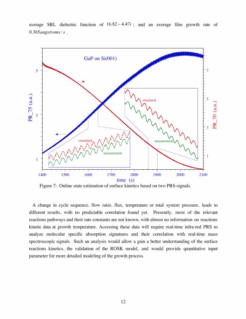
12
average SRL dielectric function of i47.482.16 - ; and an average film growth rate of
sangstroms /365.0 .
1
3
5
1
3
5
7
1400 1500 1600 1700 1800 1900 2000 2100
PR
_75
(a.u
.)
measurement
time (s)
PR
_70
(a.u
.)
GaP on Si(001)
measurement
simulated
simulated
Figure 7: Online state estimation of surface kinetics based on two PRS-signals.
A change in cycle sequence, flow ratio, flux, temperature or total system pressure, leads to
different results, with no predictable correlation found yet. Presently, most of the relevant
reactions pathways and their rate constants are not known, with almost no information on reactions
kinetic data at growth temperature. Accessing these data will require real-time infra-red PRS to
analyze molecular specific absorption signatures and their correlation with real-time mass
spectroscopic signals. Such an analysis would allow a gain a better understanding of the surface
reactions kinetics, the validation of the ROSK model, and would provide quantitative input
parameter for more detailed modeling of the growth process.

13
Figure 8:
Simulation of surface reaction
kinetics and PR response
during heteroepitaxial GaP
growth on Si under pulsed
organometallic precursors
exposure of TBP and TEG.
The molar concentrations of
the surface constituents, their
effective surface layer
thickness and the dielectric
optical properties are
calculated using equations (5)
through (15).
The simulated PR response is
compared with experimental
results obtained at j=75.1¡,
l=632.8 nm.
14.4
14.8
0 3 6 9 12 15 18
(10+
3)
R
p
(e)
time (sec)
experimentsimmulated
TBP
flux
(a
.u.)
TEG
(a)
0.3
0.6
n i(t)
n1(t)
n2(t) n
3(t)
x 2x 2 (b)
3
6d S
RL
(�)
(c)
9
18
e SRL
- eSRL
i
eSRL
r
(d)
Summary We reported the compositionally and thickness controlled growth of GaInP heterostructures,
using PRS as feedback sensor. An on-line parameter estimate of the state functions Ãn(t) using the
PRS signals is used to analyze the PRS fine structure and to provide the control signals s(t) for
TEG and TMI flows. We introduced a reduced order kinetics (ROSK) model using generalized
reaction rate parameters to describe the thickness and composition evolution of the SRL. The molar
concentrations ni in the SRL are directly linked to instantaneous growth rate and composition of the
underlying film.
AcknowledgmentsThis work has been supported by the DOD-MURI Grant F49620-95-1-0447.

14
References:1 S. M. Bedair, B. T. McDermott, Y. Ide, N. H. Karam, H. Hashemi, M. A. Tischler, M.
Timmons, J. C. L. Tarn, and N. El-Masry, J. Cryst. Growth 93, 182 (1988).2 C. R. Abernathy, J. Vac. Sci. Technol. A11, 869 (1993); L. Niinist and M. Leskel, Thin
Solid Films 225, 130 (1993).3 M. Yoshimoto, T. Hashimoto, P. Vaccaro and H. Matsunami, "In-situ RHEED observation
on surface reactions in laser-triggered chemical beam epitaxy of GaP", Appl. Surf. Sci. 79-80, 227-31 (1994).
4 D.E. Aspnes, J.P. Harbison, A.A. Studna and L.T. Florez, "Reflectance-differencespectroscopy system for real-time measurement of crystal growth", Appl. Phys. Lett.52(12), 957-9 (1988).
5 N. Kobayashi and Y. Horikoshi, "Optical Investigation on the Growth Process of GaAsduring Migration-Enhanced Epitaxy", Jpn. J. Appl. Phys. 28(11), L1880-2 (1989).
6 N. Kobayashi and Y. Horikoshi, "Spectral dependence of optical reflection during flow-ratemodulation epitaxy of gallium arsenide by the surface photo-absorption method", Jpn. J.Appl. Phys. 29, L702-L705 (1990).
7 N. Kobayashi, T. Makimoto, Y. Yamauchi and Y. Horikoshi, "In-situ monitoring ofgallium arsenide growth process in MOVPE by surface photo-absorption method", J. Cryst.Growth 107(1-4), 62-7 (1991).
8 N. Dietz and K. J. Bachmann, "Real -time monitoring of epitaxial processes by parallel-polarized reflectance spectroscopy", MRS Bull. 20 (1995) p.49-55.
9 N. Dietz and K. J. Bachmann, "p-Polarized reflectance spectroscopy: a highly sensitivereal-time monitoring technique to study surface kinetics under steady state epitaxialdeposition conditions", Vacuum 47(2), pp. 133-40 (1996).
10 N. Dietz, N. Sukidi C. Harris and K.J. Bachmann, "Real-time Monitoring of SurfaceProcesses by P-Polarized Reflectance", J. Vac. Sci. & Technol. A 15(3) p. 807-815(1997).
11 M. Ebert, K.A. Bell, S. D. Yoo, G. D. Powell, and D. E. Aspnes, "Integrated real-timespectroscopic ellipsometric and reflectance difference measurements in a commercialOMCVD reactor", J. Vac. Sci. & Technol. submitted, (1999).
12 D. E. Aspnes, "Optical approaches to determine near-surface compositions during epitaxy",J. Vac. Sci. & Technol. A14, 960-966 (1996).
13 N. Dietz, A. Miller and K. J. Bachmann, "Real -time monitoring of homoepitaxial andheteroepitaxial processes by p-polarized reflectance spectroscopy", J. Vac. Sci. & Technol.A 13, 153-155 (1995).
14 N. Dietz, A. Miller, J. T. Kelliher, D. Venables and K. J. Bachmann, "Migration-enhancedpulsed chemical beam epitaxy of GaP on Si(001)", J. Cryst. Growth 150 (1-4) 691-695(1995).
15 N. Dietz, U. Rossow, D. Aspnes and K.J. Bachmann, "Real-Time Optical Monitoring ofEpitaxial Growth: Pulsed Chemical Beam Epitaxy of GaP and InP Homoepitaxy andHeteroepitaxy on Si", JEM 24(11) 1571-76 (1995).
16 K. J. Bachmann, N. Dietz, A. E. Miller, D. Venables and J. T. Kelliher, "Heteroepitaxy oflattice-matched compound semiconductors on silicon", J. Vac. Sci. & Technol. A 13,p.696-704 (1995).
17 K. J. Bachmann, U. Rossow, N. Sukidi, H. Castleberry and N. Dietz, " Heteroepitaxy ofNearly Lattice-Matched Tetrahedrally Coordinated Compound Semiconductors on Si(100)",J. Vac. Sci. & Technol. B 14, 3019 (1996)

15
18 N. Dietz, U. Rossow, D. E. Aspnes and K.J. Bachmann, "Real-Time Optical Monitoringof Heteroepitaxial Growth Processes on Si under Pulsed Chemical Beam EpitaxyConditions", Appl. Surf. Sci. 102, p.47-51 (1996).
19 N. Dietz, N. Sukidi, C. Harris and K.J. Bachmann, "Real-time Characterization of theOptical Properties of an ultra-thin Surface Reaction Layer during Growth", Mat. Res. Soc.Symp. Proc. 441, 39-44 (1997).
20 K.J. Bachmann, N. Sukidi, N. Dietz, C. Hoepfner, S. LeSure, H.T. Tran, S. Beeler, K.Ito and H.T. Banks, "Real-time monitoring of the kinetics of pulsed chemical beam epitaxyby p-polarized reflectance", J. Cryst. Growth 183, 323-337 (1998).
21 N. Dietz, N. Sukidi, C. Harris and K.J. Bachmann, " Real-time Monitoring ofHeteroepitaxial GaxIn1-xP/GaP Growth by P-Polarized Reflectance", Conf. Proc. ofIPRM-9Õ97, ISSN 1092-8669, p. 521 (1997).
22 K. J. Bachmann, C. Hoepfner, N. Sukidi, A.E. Miller, C. Harris, D. E. Aspnes, N. Dietz,H.T. Tran, S. Beeler, K. Ito, H. T. Banks and U. Rossow, "Molecular Layer Epitaxy byReal-Time Optical Process Monitoring", Appl. Surf. Sci. 112, 38-47 (1997).
23 N. Dietz, K. Ito, Real-time optical characterization of GaP heterostructures by p-polarizedreflectance, Thin Solid Films 313-314(1-2) (1998) 615-620.
24 J.T. Kelliher, N. Dietz and K.J. Bachmann, "The Kinetics of Chemical Beam Epitaxy ofGallium Phosphide", Proc. SOTAPOCS 18, Honolulu, Hawai, The ElectrochemicalSociety, Pennington, NJ, p. 17 (1994).
25 A. J. Murrell, A. T. S. Wee, D. H. Fairbrother, N. K. Singh, J. S. Foord, G. J. Daviesand D. A. Andrews, J. Crys. Growth 105, 199-202 (1990).
26 K.J. Bachmann, U. Rossow and N. Dietz, "Real-Time Monitoring of HeteroepitaxialGrowth Processes on the Silicon (001) surface by P-Polarized Reflectance Spectroscopy",Mater. Sci. & Eng. B 37(1-3) 472-478 (1995).
27 D. E. Aspnes, "Minimal-data approaches for determining outer-layer dielectric responses offilms from kinetic reflectometric and ellipsometric measurements", J. Opt. Soc. Am. A 10,974-83 (1993).
28 D. E. Aspnes, "Minimal-data approaches for determining outer-layer dielectric responses offilms from kinetic reflectometric and ellipsometric measurements", Appl. Phys. Lett. 62,343-5 (1993).
29 D. E. Aspnes, US Patent 5,277,747, issued 11 Jan. 1994.30 K.Ito and K. Xiong, "New Gaussian filter for nonlinear filtering problems", IEEE, Tras.
Automatic Control, accepted for publication (1998).31 S. Beeler, H.T. Tran and N. Dietz, "Representation of GaP Formation by a Reduced Order
Model using P-Polarized Reflectance Measurements", J. Appl. Phys., submitted (1998).
Related Documents