Read Disturb Fault Detection in STT-MRAM Rajendra Bishnoi Mojtaba Ebrahimi Fabian Oboril Mehdi B. Tahoori Karlsruhe Institute of Technology, Karlsruhe, Germany E-mails: {rajendra.bishnoi, mojtaba.ebrahimi, fabian.oboril, mehdi.tahoori}@kit.edu Abstract—Spin Transfer Torque Magnetic Random Access Memory (STT-MRAM) has potential to become a universal memory technology because of its various advantageous features such as high density, non-volatility, scalability, high endurance and CMOS compatibility. However, read disturb is a major reliability issue in which a read operation can lead to a bit- flip, because read and write current share the same path. This major reliability challenge is growing with technology scaling as read to write current ratio decreases. In this paper, we propose a circuit-level technique to detect read disturb by sensing the current during the read operation. Experimental results show that the proposed technique can effectively detect read disturb at the cost of negligible power and area overhead. I. I NTRODUCTION As technology scales down, current memory technologies such as SRAM and DRAM are facing challenges in terms of scalability and high leakage [1, 2]. Therefore, industry is actively searching for alternatives, especially in the area of non-volatile memories as these promise close-to-zero leakage. However, many of these non-volatile memory technologies such as NAND-Flash suffer from endurance issues [3]. Spin Transfer Torque Magnetic Random Access Memory (STT- MRAM) is an emerging memory technology which is not only non-volatile but is also scalable and has a high endurance [4–6]. In addition to that, it has a high density, is CMOS- compatible and soft-error immune [2, 7]. Despite various advantageous features, STT-MRAM is facing various reliability challenges including write failure, decision failure, retention failure and failures due to read disturb [8, 9]. Retention failures are due to the inherent thermal instability of STT-MRAM, which can lead to a flip of the bit-cell content, although no memory access is performed. In contrast, a write failure occurs when the bit-cell does not flip to its required value during the given write period. This can happen, since the write process in STT-MRAM is of stochastic nature. If it is not possible to distinguish between the two states of a bit-cell during a read operation it is a decision failure, while read disturb means that the bit-cell value is accidentally flipped during a read operation. Write and decision failures can be resolved either by increasing the write and the read time period, respectively, or by increasing their corresponding current values [10]. On the other hand, the retention failure can be handled at the device- level by exploiting the thermal stability factor. Read disturb can also be resolved by widening the margin between read and write current which can be achieved either by increasing the write current or reducing the read current. However, reducing the read current increases not only the read latency but also the chances of decision failures [11]. Moreover, STT-MRAM has already a high write energy as it requires a high current to flip the bit-cell [12, 13], and a further increase in write current is hence not a feasible solution. Furthermore, recently it has been shown that the read disturb rate is growing with technology scaling [9] and is going to be a major reliability issue in future technology nodes [8]. Therefore, employing efficient read disturb mitigation techniques is of decisive importance. The pulsed read [14] and disruptive reading and restoring [15] schemes are two techniques to alleviate read disturb in STT-MRAM. In addition, some bit-cell architectures are proposed to mitigate read disturb [7, 16–18]. Moreover, there is a device-level scheme proposed in which the read disturb rate can be reduced by increasing the thermal stability factor [12]. However, while all of these techniques can reduce the read disturb rate, they impose excessive access time, area and/or power costs. As a consequence, these mitigation approaches are not the best way to achieve efficient designs. Instead, low- cost detection techniques paired with efficient error correction approaches should be considered for future STT-MRAM tech- nologies. In this paper, we propose a low-cost circuit-level technique to detect read disturb in STT-MRAM. This technique exploits the fact that during a read operation the read current is either always larger or always smaller than the reference current. However, if a read disturb occurs, the ratio of the read current to the reference current flips. This observation is used by our technique to create an acknowledgement signal, which indicates the occurrence of a read disturb. Since the read current is unidirectional, read disturb can only affect one logic value. Therefore, our read disturb detection circuit is only activated for that particular logic value which results in a very low power penalty. Moreover, there is no timing penalty as our detection circuit is isolated using a current mirror from the actual read process. Our experimental results show that the proposed read disturb detection technique can detect upto 95 % of the total read disturb faults and imposes only 0.8% and 0.2% area and power overhead, respectively. The rest of the paper is organized as follows. Section II consists of the basics of the STT-MRAM technology and the related work. In Section III, the proposed technique is explained. Section IV presents the experimental results and finally, Section V concludes the paper. II. BACKGROUND A. Spin Transfer Torque Memory STT-MRAM consists of magnetic tunnel junction (MTJ) cells to store the data. An MTJ cell consists of a barrier oxide layer, sandwiched by two ferromagnetic layers. The fer- romagnetic layer whose magnetic orientation is always fixed, is known as Reference Layer (RL), while the other one, whose magnetic orientation can be freely rotated, is named Free Layer (FL) (see Figure 1). In an MTJ cell, values are stored in Paper 23.3 INTERNATIONAL TEST CONFERENCE 1 978-1-4799-4722-5/14/$31.00 2014 IEEE

Welcome message from author
This document is posted to help you gain knowledge. Please leave a comment to let me know what you think about it! Share it to your friends and learn new things together.
Transcript
Read Disturb Fault Detection in STT-MRAM
Rajendra Bishnoi Mojtaba Ebrahimi Fabian Oboril Mehdi B. TahooriKarlsruhe Institute of Technology, Karlsruhe, Germany
E-mails: {rajendra.bishnoi, mojtaba.ebrahimi, fabian.oboril, mehdi.tahoori}@kit.edu
Abstract—Spin Transfer Torque Magnetic Random AccessMemory (STT-MRAM) has potential to become a universalmemory technology because of its various advantageous featuressuch as high density, non-volatility, scalability, high enduranceand CMOS compatibility. However, read disturb is a majorreliability issue in which a read operation can lead to a bit-flip, because read and write current share the same path. Thismajor reliability challenge is growing with technology scaling asread to write current ratio decreases. In this paper, we proposea circuit-level technique to detect read disturb by sensing thecurrent during the read operation. Experimental results showthat the proposed technique can effectively detect read disturbat the cost of negligible power and area overhead.
I. INTRODUCTIONAs technology scales down, current memory technologies
such as SRAM and DRAM are facing challenges in termsof scalability and high leakage [1, 2]. Therefore, industry isactively searching for alternatives, especially in the area ofnon-volatile memories as these promise close-to-zero leakage.However, many of these non-volatile memory technologiessuch as NAND-Flash suffer from endurance issues [3]. SpinTransfer Torque Magnetic Random Access Memory (STT-MRAM) is an emerging memory technology which is not onlynon-volatile but is also scalable and has a high endurance[4–6]. In addition to that, it has a high density, is CMOS-compatible and soft-error immune [2, 7].
Despite various advantageous features, STT-MRAM isfacing various reliability challenges including write failure,decision failure, retention failure and failures due to readdisturb [8, 9]. Retention failures are due to the inherent thermalinstability of STT-MRAM, which can lead to a flip of thebit-cell content, although no memory access is performed. Incontrast, a write failure occurs when the bit-cell does not flipto its required value during the given write period. This canhappen, since the write process in STT-MRAM is of stochasticnature. If it is not possible to distinguish between the two statesof a bit-cell during a read operation it is a decision failure,while read disturb means that the bit-cell value is accidentallyflipped during a read operation.
Write and decision failures can be resolved either byincreasing the write and the read time period, respectively, orby increasing their corresponding current values [10]. On theother hand, the retention failure can be handled at the device-level by exploiting the thermal stability factor. Read disturbcan also be resolved by widening the margin between read andwrite current which can be achieved either by increasing thewrite current or reducing the read current. However, reducingthe read current increases not only the read latency but also thechances of decision failures [11]. Moreover, STT-MRAM hasalready a high write energy as it requires a high current to flipthe bit-cell [12, 13], and a further increase in write current is
hence not a feasible solution. Furthermore, recently it has beenshown that the read disturb rate is growing with technologyscaling [9] and is going to be a major reliability issue infuture technology nodes [8]. Therefore, employing efficientread disturb mitigation techniques is of decisive importance.
The pulsed read [14] and disruptive reading and restoring[15] schemes are two techniques to alleviate read disturbin STT-MRAM. In addition, some bit-cell architectures areproposed to mitigate read disturb [7, 16–18]. Moreover, there isa device-level scheme proposed in which the read disturb ratecan be reduced by increasing the thermal stability factor [12].However, while all of these techniques can reduce the readdisturb rate, they impose excessive access time, area and/orpower costs. As a consequence, these mitigation approachesare not the best way to achieve efficient designs. Instead, low-cost detection techniques paired with efficient error correctionapproaches should be considered for future STT-MRAM tech-nologies.
In this paper, we propose a low-cost circuit-level techniqueto detect read disturb in STT-MRAM. This technique exploitsthe fact that during a read operation the read current is eitheralways larger or always smaller than the reference current.However, if a read disturb occurs, the ratio of the read currentto the reference current flips. This observation is used byour technique to create an acknowledgement signal, whichindicates the occurrence of a read disturb. Since the readcurrent is unidirectional, read disturb can only affect one logicvalue. Therefore, our read disturb detection circuit is onlyactivated for that particular logic value which results in a verylow power penalty. Moreover, there is no timing penalty asour detection circuit is isolated using a current mirror fromthe actual read process. Our experimental results show thatthe proposed read disturb detection technique can detect upto95 % of the total read disturb faults and imposes only 0.8%and 0.2% area and power overhead, respectively.
The rest of the paper is organized as follows. Section IIconsists of the basics of the STT-MRAM technology andthe related work. In Section III, the proposed technique isexplained. Section IV presents the experimental results andfinally, Section V concludes the paper.
II. BACKGROUND
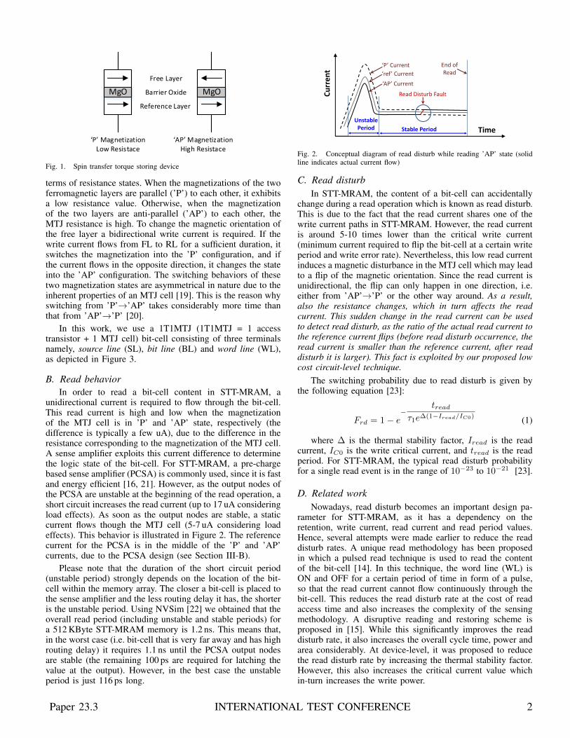
A. Spin Transfer Torque MemorySTT-MRAM consists of magnetic tunnel junction (MTJ)
cells to store the data. An MTJ cell consists of a barrieroxide layer, sandwiched by two ferromagnetic layers. The fer-romagnetic layer whose magnetic orientation is always fixed,is known as Reference Layer (RL), while the other one, whosemagnetic orientation can be freely rotated, is named Free Layer(FL) (see Figure 1). In an MTJ cell, values are stored in
Paper 23.3 INTERNATIONAL TEST CONFERENCE 1978-1-4799-4722-5/14/$31.00 2014 IEEE
MgO MgO
Free Layer
Barrier Oxide
Reference Layer
‘P’ MagnetizationLow Resistace
‘AP’ MagnetizationHigh Resistace
Fig. 1. Spin transfer torque storing device
terms of resistance states. When the magnetizations of the twoferromagnetic layers are parallel (’P’) to each other, it exhibitsa low resistance value. Otherwise, when the magnetizationof the two layers are anti-parallel (’AP’) to each other, theMTJ resistance is high. To change the magnetic orientation ofthe free layer a bidirectional write current is required. If thewrite current flows from FL to RL for a sufficient duration, itswitches the magnetization into the ’P’ configuration, and ifthe current flows in the opposite direction, it changes the stateinto the ’AP’ configuration. The switching behaviors of thesetwo magnetization states are asymmetrical in nature due to theinherent properties of an MTJ cell [19]. This is the reason whyswitching from ’P’→’AP’ takes considerably more time thanthat from ’AP’→’P’ [20].
In this work, we use a 1T1MTJ (1T1MTJ = 1 accesstransistor + 1 MTJ cell) bit-cell consisting of three terminalsnamely, source line (SL), bit line (BL) and word line (WL),as depicted in Figure 3.
B. Read behaviorIn order to read a bit-cell content in STT-MRAM, a
unidirectional current is required to flow through the bit-cell.This read current is high and low when the magnetizationof the MTJ cell is in ’P’ and ’AP’ state, respectively (thedifference is typically a few uA), due to the difference in theresistance corresponding to the magnetization of the MTJ cell.A sense amplifier exploits this current difference to determinethe logic state of the bit-cell. For STT-MRAM, a pre-chargebased sense amplifier (PCSA) is commonly used, since it is fastand energy efficient [16, 21]. However, as the output nodes ofthe PCSA are unstable at the beginning of the read operation, ashort circuit increases the read current (up to 17 uA consideringload effects). As soon as the output nodes are stable, a staticcurrent flows though the MTJ cell (5-7 uA considering loadeffects). This behavior is illustrated in Figure 2. The referencecurrent for the PCSA is in the middle of the ’P’ and ’AP’currents, due to the PCSA design (see Section III-B).
Please note that the duration of the short circuit period(unstable period) strongly depends on the location of the bit-cell within the memory array. The closer a bit-cell is placed tothe sense amplifier and the less routing delay it has, the shorteris the unstable period. Using NVSim [22] we obtained that theoverall read period (including unstable and stable periods) fora 512 KByte STT-MRAM memory is 1.2 ns. This means that,in the worst case (i.e. bit-cell that is very far away and has highrouting delay) it requires 1.1 ns until the PCSA output nodesare stable (the remaining 100 ps are required for latching thevalue at the output). However, in the best case the unstableperiod is just 116 ps long.
‘P’ Current
‘AP’ Current
‘ref’ Current
Read Disturb Fault
Time
Cu
rre
nt
Unstable Period Stable Period
End of Read
Fig. 2. Conceptual diagram of read disturb while reading ’AP’ state (solidline indicates actual current flow)
C. Read disturbIn STT-MRAM, the content of a bit-cell can accidentally
change during a read operation which is known as read disturb.This is due to the fact that the read current shares one of thewrite current paths in STT-MRAM. However, the read currentis around 5-10 times lower than the critical write current(minimum current required to flip the bit-cell at a certain writeperiod and write error rate). Nevertheless, this low read currentinduces a magnetic disturbance in the MTJ cell which may leadto a flip of the magnetic orientation. Since the read current isunidirectional, the flip can only happen in one direction, i.e.either from ’AP’→’P’ or the other way around. As a result,also the resistance changes, which in turn affects the readcurrent. This sudden change in the read current can be usedto detect read disturb, as the ratio of the actual read current tothe reference current flips (before read disturb occurrence, theread current is smaller than the reference current, after readdisturb it is larger). This fact is exploited by our proposed lowcost circuit-level technique.
The switching probability due to read disturb is given bythe following equation [23]:
Frd = 1− e−
treadτ1e∆(1−Iread/IC0) (1)
where ∆ is the thermal stability factor, Iread is the readcurrent, IC0 is the write critical current, and tread is the readperiod. For STT-MRAM, the typical read disturb probabilityfor a single read event is in the range of 10−23 to 10−21 [23].
D. Related workNowadays, read disturb becomes an important design pa-
rameter for STT-MRAM, as it has a dependency on theretention, write current, read current and read period values.Hence, several attempts were made earlier to reduce the readdisturb rates. A unique read methodology has been proposedin which a pulsed read technique is used to read the contentof the bit-cell [14]. In this technique, the word line (WL) isON and OFF for a certain period of time in form of a pulse,so that the read current cannot flow continuously through thebit-cell. This reduces the read disturb rate at the cost of readaccess time and also increases the complexity of the sensingmethodology. A disruptive reading and restoring scheme isproposed in [15]. While this significantly improves the readdisturb rate, it also increases the overall cycle time, power andarea considerably. At device-level, it was proposed to reducethe read disturb rate by increasing the thermal stability factor.However, this also increases the critical current value whichin-turn increases the write power.
Paper 23.3 INTERNATIONAL TEST CONFERENCE 2
MgO
Source line
Bit line
FL
RLRea
d c
urr
ent
MgO
Source line
Bit line
RL
FL
Word line
Rea
d c
urr
ent
Word line
(a) Conventional bit-cell
(b) Reverse connected bit-cell
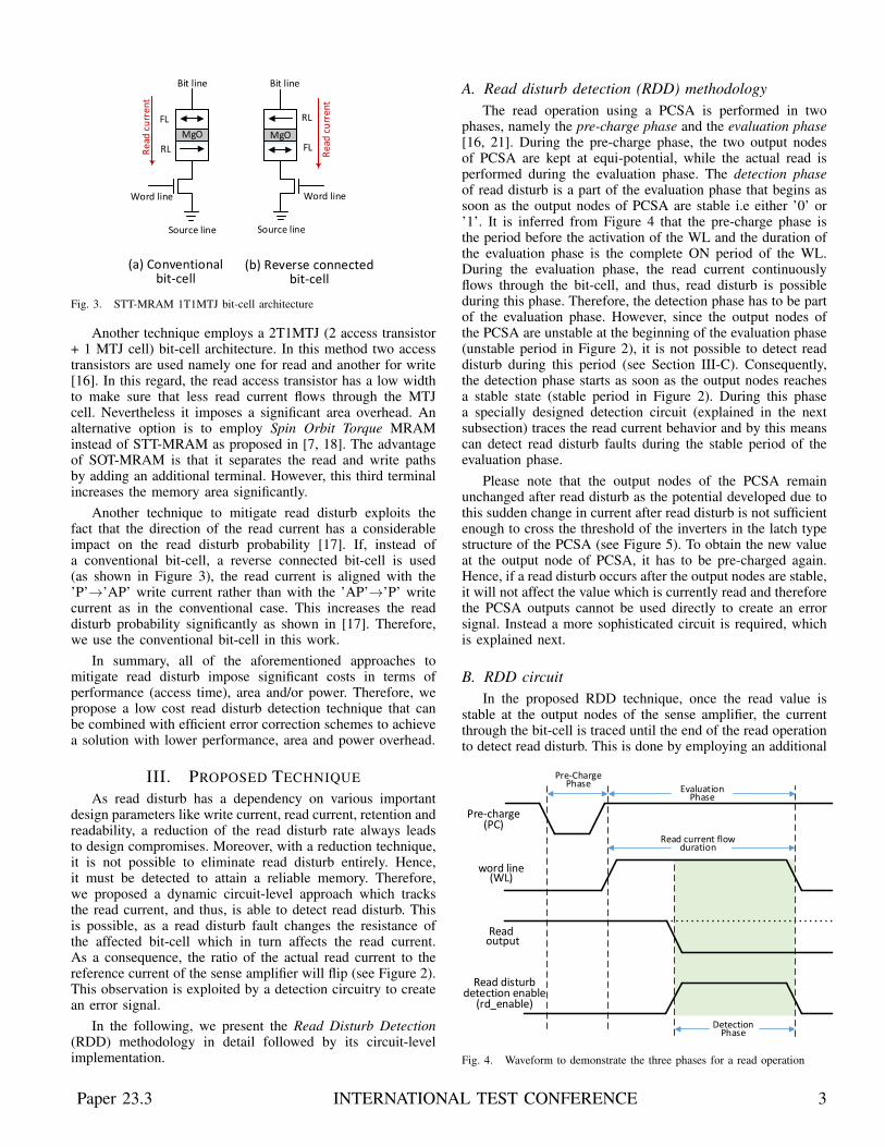
Fig. 3. STT-MRAM 1T1MTJ bit-cell architecture
Another technique employs a 2T1MTJ (2 access transistor+ 1 MTJ cell) bit-cell architecture. In this method two accesstransistors are used namely one for read and another for write[16]. In this regard, the read access transistor has a low widthto make sure that less read current flows through the MTJcell. Nevertheless it imposes a significant area overhead. Analternative option is to employ Spin Orbit Torque MRAMinstead of STT-MRAM as proposed in [7, 18]. The advantageof SOT-MRAM is that it separates the read and write pathsby adding an additional terminal. However, this third terminalincreases the memory area significantly.
Another technique to mitigate read disturb exploits thefact that the direction of the read current has a considerableimpact on the read disturb probability [17]. If, instead ofa conventional bit-cell, a reverse connected bit-cell is used(as shown in Figure 3), the read current is aligned with the’P’→’AP’ write current rather than with the ’AP’→’P’ writecurrent as in the conventional case. This increases the readdisturb probability significantly as shown in [17]. Therefore,we use the conventional bit-cell in this work.
In summary, all of the aforementioned approaches tomitigate read disturb impose significant costs in terms ofperformance (access time), area and/or power. Therefore, wepropose a low cost read disturb detection technique that canbe combined with efficient error correction schemes to achievea solution with lower performance, area and power overhead.
III. PROPOSED TECHNIQUE
As read disturb has a dependency on various importantdesign parameters like write current, read current, retention andreadability, a reduction of the read disturb rate always leadsto design compromises. Moreover, with a reduction technique,it is not possible to eliminate read disturb entirely. Hence,it must be detected to attain a reliable memory. Therefore,we proposed a dynamic circuit-level approach which tracksthe read current, and thus, is able to detect read disturb. Thisis possible, as a read disturb fault changes the resistance ofthe affected bit-cell which in turn affects the read current.As a consequence, the ratio of the actual read current to thereference current of the sense amplifier will flip (see Figure 2).This observation is exploited by a detection circuitry to createan error signal.
In the following, we present the Read Disturb Detection(RDD) methodology in detail followed by its circuit-levelimplementation.
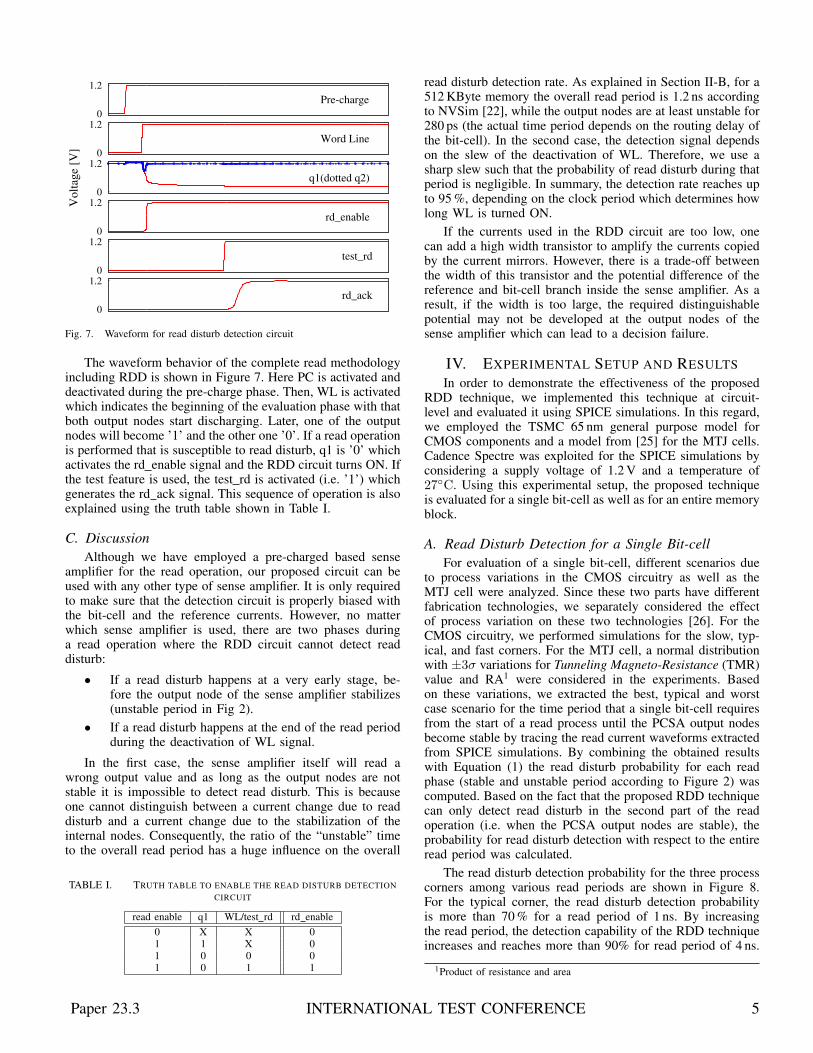
A. Read disturb detection (RDD) methodologyThe read operation using a PCSA is performed in two
phases, namely the pre-charge phase and the evaluation phase[16, 21]. During the pre-charge phase, the two output nodesof PCSA are kept at equi-potential, while the actual read isperformed during the evaluation phase. The detection phaseof read disturb is a part of the evaluation phase that begins assoon as the output nodes of PCSA are stable i.e either ’0’ or’1’. It is inferred from Figure 4 that the pre-charge phase isthe period before the activation of the WL and the duration ofthe evaluation phase is the complete ON period of the WL.During the evaluation phase, the read current continuouslyflows through the bit-cell, and thus, read disturb is possibleduring this phase. Therefore, the detection phase has to be partof the evaluation phase. However, since the output nodes ofthe PCSA are unstable at the beginning of the evaluation phase(unstable period in Figure 2), it is not possible to detect readdisturb during this period (see Section III-C). Consequently,the detection phase starts as soon as the output nodes reachesa stable state (stable period in Figure 2). During this phasea specially designed detection circuit (explained in the nextsubsection) traces the read current behavior and by this meanscan detect read disturb faults during the stable period of theevaluation phase.
Please note that the output nodes of the PCSA remainunchanged after read disturb as the potential developed due tothis sudden change in current after read disturb is not sufficientenough to cross the threshold of the inverters in the latch typestructure of the PCSA (see Figure 5). To obtain the new valueat the output node of PCSA, it has to be pre-charged again.Hence, if a read disturb occurs after the output nodes are stable,it will not affect the value which is currently read and thereforethe PCSA outputs cannot be used directly to create an errorsignal. Instead a more sophisticated circuit is required, whichis explained next.
B. RDD circuitIn the proposed RDD technique, once the read value is
stable at the output nodes of the sense amplifier, the currentthrough the bit-cell is traced until the end of the read operationto detect read disturb. This is done by employing an additional
word line(WL)
q1(high Read ‘P’
low Read ‘AP’)read enable
( low write operation high read operation )
rd_enable (read disturb
detection enable)
Read disturb detection enable
(rd_enable)
Read current flow duration
WL/test_rd
connected to NMOS ‘N9'
word line(WL)
Pre-charge(PC)
Read output
Evaluation Phase
Pre-Charge Phase
Detection Phase
WL: For actual scenario
Test_rd: To test the detection circuit
Fig. 4. Waveform to demonstrate the three phases for a read operation
Paper 23.3 INTERNATIONAL TEST CONFERENCE 3
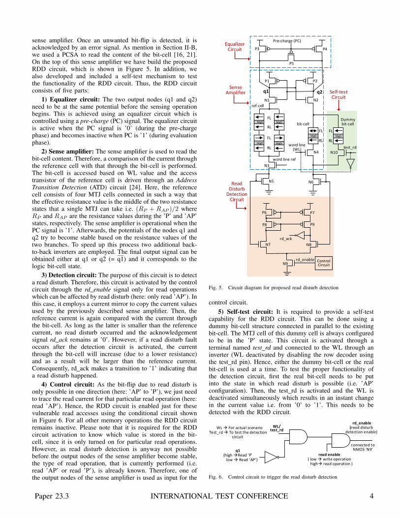
sense amplifier. Once an unwanted bit-flip is detected, it isacknowledged by an error signal. As mention in Section II-B,we used a PCSA to read the content of the bit-cell [16, 21].On the top of this sense amplifier we have build the proposedRDD circuit, which is shown in Figure 5. In addition, wealso developed and included a self-test mechanism to testthe functionality of the RDD circuit. Thus, the RDD circuitconsists of five parts:
1) Equalizer circuit: The two output nodes (q1 and q2)need to be at the same potential before the sensing operationbegins. This is achieved using an equalizer circuit which iscontrolled using a pre-charge (PC) signal. The equalizer circuitis active when the PC signal is ’0’ (during the pre-chargephase) and becomes inactive when PC is ’1’ (during evaluationphase).
2) Sense amplifier: The sense amplifier is used to read thebit-cell content. Therefore, a comparison of the current throughthe reference cell with that through the bit-cell is performed.The bit-cell is accessed based on WL value and the accesstransistor of the reference cell is driven through an AddressTransition Detection (ATD) circuit [24]. Here, the referencecell consists of four MTJ cells connected in such a way thatthe effective resistance value is the middle of the two resistancestates that a single MTJ can take i.e. (RP + RAP )/2 whereRP and RAP are the resistance values during the ’P’ and ’AP’states, respectively. The sense amplifier is operational when thePC signal is ’1’. Afterwards, the potentials of the nodes q1 andq2 try to become stable based on the resistance values of thetwo branches. To speed up this process two additional back-to-back inverters are employed. The final output signal can beobtained either at q1 or q2 (= q1) and it corresponds to thelogic bit-cell state.
3) Detection circuit: The purpose of this circuit is to detecta read disturb. Therefore, this circuit is activated by the controlcircuit through the rd enable signal only for read operationswhich can be affected by read disturb (here: only read ’AP’). Inthis case, it employs a current mirror to copy the current valuesused by the previously described sense amplifier. Then, thereference current is again compared with the current throughthe bit-cell. As long as the latter is smaller than the referencecurrent, no read disturb occurred and the acknowledgementsignal rd ack remains at ’0’. However, if a read disturb faultoccurs after the detection circuit is activated, the currentthrough the bit-cell will increase (due to a lower resistance)and as a result will be larger than the reference current.Consequently, rd ack makes a transition to ’1’ indicating thata read disturb happened.
4) Control circuit: As the bit-flip due to read disturb isonly possible in one direction (here: ’AP’ to ’P’), we just needto trace the read current for that particular read operation (here:read ’AP’). Hence, the RDD circuit is enabled just for thesevulnerable read accesses using the conditional circuit shownin Figure 6. For all other memory operations the RDD circuitremains inactive. Please note that it is required for the RDDcircuit activation to know which value is stored in the bit-cell, since it is only turned on for particular read operations.However, as read disturb detection is anyway not possiblebefore the output nodes of the sense amplifier become stable,the type of read operation, that is currently performed (i.e.read ’AP’ or read ’P’), is already known. Therefore, one ofthe output nodes of the sense amplifier is used as input for the
RL
MgO MgO
MgO MgO
FL
RL
FL
RLFL
Pre-charge (PC)
q2q1
word line(WL)
word line ref
bit-cell
ref-cell
rd_enable
rd_ack
P1 P2
P3 P4
P5
P6 P7
P8 P9
N1 N2
N3
N4
N5 N6
N7 N8
N9
RL
FL
N10
Dummy bit-cell
test_rd
Self-test Circuit
Equalizer Circuit
Sense Amplifier
Read Disturb
Detection Circuit
Control Circuit
MgO MgO
Fig. 5. Circuit diagram for proposed read disturb detection
control circuit.5) Self-test circuit: It is required to provide a self-test
capability for the RDD circuit. This can be done using adummy bit-cell structure connected in parallel to the existingbit-cell. The MTJ cell of this dummy cell is always configuredto be in the ’P’ state. This circuit is activated through aterminal named test rd and connected to the WL through aninverter (WL deactivated by disabling the row decoder usingthe test rd pin). Hence, either the dummy bit-cell or the realbit-cell is used at a time. To test the proper functionality ofthe detection circuit, first the real bit-cell needs to be putinto the state in which read disturb is possible (i.e. ’AP’configuration). Then, the test rd is activated and the WL isdeactivated simultaneously which results in an instant changein the current value i.e. from ’0’ to ’1’. This needs to bedetected with the RDD circuit.
word line(WL)
q1(high Read ‘P’
low Read ‘AP’)read enable
( low write operation high read operation )
rd_enable (read disturb
detection enable)
Read disturb detection enable
(rd_enable)
Read current flow duration
WL/test_rd
connected to NMOS ‘N9'
word line(WL)
Pre-charge(PC)
Read output
Evaluation Phase
Pre-Charge Phase
Detection Phase
WL For actual scenario Test_rd To test the detection
circuit
Fig. 6. Control circuit to trigger the read disturb detection
Paper 23.3 INTERNATIONAL TEST CONFERENCE 4
0
1.2
Pre-charge
0
1.2
Word Line
0
1.2
Volt
age
[V]
q1(dotted q2)
0
1.2
rd_enable
0
1.2
test_rd
0
1.2
rd_ack
Fig. 7. Waveform for read disturb detection circuit
The waveform behavior of the complete read methodologyincluding RDD is shown in Figure 7. Here PC is activated anddeactivated during the pre-charge phase. Then, WL is activatedwhich indicates the beginning of the evaluation phase with thatboth output nodes start discharging. Later, one of the outputnodes will become ’1’ and the other one ’0’. If a read operationis performed that is susceptible to read disturb, q1 is ’0’ whichactivates the rd enable signal and the RDD circuit turns ON. Ifthe test feature is used, the test rd is activated (i.e. ’1’) whichgenerates the rd ack signal. This sequence of operation is alsoexplained using the truth table shown in Table I.
C. DiscussionAlthough we have employed a pre-charged based sense
amplifier for the read operation, our proposed circuit can beused with any other type of sense amplifier. It is only requiredto make sure that the detection circuit is properly biased withthe bit-cell and the reference currents. However, no matterwhich sense amplifier is used, there are two phases duringa read operation where the RDD circuit cannot detect readdisturb:
• If a read disturb happens at a very early stage, be-fore the output node of the sense amplifier stabilizes(unstable period in Fig 2).
• If a read disturb happens at the end of the read periodduring the deactivation of WL signal.
In the first case, the sense amplifier itself will read awrong output value and as long as the output nodes are notstable it is impossible to detect read disturb. This is becauseone cannot distinguish between a current change due to readdisturb and a current change due to the stabilization of theinternal nodes. Consequently, the ratio of the “unstable” timeto the overall read period has a huge influence on the overall
TABLE I. TRUTH TABLE TO ENABLE THE READ DISTURB DETECTIONCIRCUIT
read enable q1 WL/test rd rd enable0 X X 01 1 X 01 0 0 01 0 1 1
read disturb detection rate. As explained in Section II-B, for a512 KByte memory the overall read period is 1.2 ns accordingto NVSim [22], while the output nodes are at least unstable for280 ps (the actual time period depends on the routing delay ofthe bit-cell). In the second case, the detection signal dependson the slew of the deactivation of WL. Therefore, we use asharp slew such that the probability of read disturb during thatperiod is negligible. In summary, the detection rate reaches upto 95 %, depending on the clock period which determines howlong WL is turned ON.
If the currents used in the RDD circuit are too low, onecan add a high width transistor to amplify the currents copiedby the current mirrors. However, there is a trade-off betweenthe width of this transistor and the potential difference of thereference and bit-cell branch inside the sense amplifier. As aresult, if the width is too large, the required distinguishablepotential may not be developed at the output nodes of thesense amplifier which can lead to a decision failure.
IV. EXPERIMENTAL SETUP AND RESULTSIn order to demonstrate the effectiveness of the proposed
RDD technique, we implemented this technique at circuit-level and evaluated it using SPICE simulations. In this regard,we employed the TSMC 65 nm general purpose model forCMOS components and a model from [25] for the MTJ cells.Cadence Spectre was exploited for the SPICE simulations byconsidering a supply voltage of 1.2 V and a temperature of27◦C. Using this experimental setup, the proposed techniqueis evaluated for a single bit-cell as well as for an entire memoryblock.
A. Read Disturb Detection for a Single Bit-cellFor evaluation of a single bit-cell, different scenarios due
to process variations in the CMOS circuitry as well as theMTJ cell were analyzed. Since these two parts have differentfabrication technologies, we separately considered the effectof process variation on these two technologies [26]. For theCMOS circuitry, we performed simulations for the slow, typ-ical, and fast corners. For the MTJ cell, a normal distributionwith ±3σ variations for Tunneling Magneto-Resistance (TMR)value and RA1 were considered in the experiments. Basedon these variations, we extracted the best, typical and worstcase scenario for the time period that a single bit-cell requiresfrom the start of a read process until the PCSA output nodesbecome stable by tracing the read current waveforms extractedfrom SPICE simulations. By combining the obtained resultswith Equation (1) the read disturb probability for each readphase (stable and unstable period according to Figure 2) wascomputed. Based on the fact that the proposed RDD techniquecan only detect read disturb in the second part of the readoperation (i.e. when the PCSA output nodes are stable), theprobability for read disturb detection with respect to the entireread period was calculated.
The read disturb detection probability for the three processcorners among various read periods are shown in Figure 8.For the typical corner, the read disturb detection probabilityis more than 70 % for a read period of 1 ns. By increasingthe read period, the detection capability of the RDD techniqueincreases and reaches more than 90% for read period of 4 ns.
1Product of resistance and area
Paper 23.3 INTERNATIONAL TEST CONFERENCE 5
65%
70%
75%
80%
85%
90%
95%
1.0 1.5 2.0 2.5 3.0 3.5 4.0
Rea
d D
istu
rb D
etec
tion P
robab
ilit
y
Read Period [ns]
Fig. 8. Probability of read disturb detection vs read period for a single bit-cellconsidering process variation
A similar trend can be seen for the worst case and best caseas well.
B. Read Disturb Detection for a Memory ArrayFor the evaluation of the efficiency of our proposed
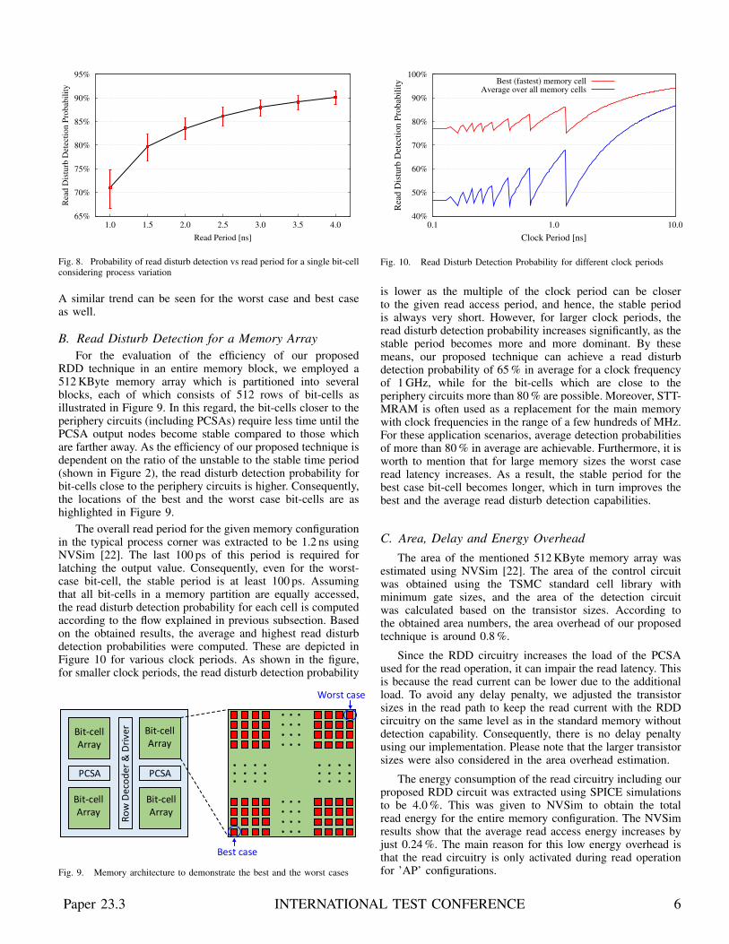
RDD technique in an entire memory block, we employed a512 KByte memory array which is partitioned into severalblocks, each of which consists of 512 rows of bit-cells asillustrated in Figure 9. In this regard, the bit-cells closer to theperiphery circuits (including PCSAs) require less time until thePCSA output nodes become stable compared to those whichare farther away. As the efficiency of our proposed technique isdependent on the ratio of the unstable to the stable time period(shown in Figure 2), the read disturb detection probability forbit-cells close to the periphery circuits is higher. Consequently,the locations of the best and the worst case bit-cells are ashighlighted in Figure 9.
The overall read period for the given memory configurationin the typical process corner was extracted to be 1.2 ns usingNVSim [22]. The last 100 ps of this period is required forlatching the output value. Consequently, even for the worst-case bit-cell, the stable period is at least 100 ps. Assumingthat all bit-cells in a memory partition are equally accessed,the read disturb detection probability for each cell is computedaccording to the flow explained in previous subsection. Basedon the obtained results, the average and highest read disturbdetection probabilities were computed. These are depicted inFigure 10 for various clock periods. As shown in the figure,for smaller clock periods, the read disturb detection probability
Ro
w D
eco
der
& D
rive
r
PCSA PCSA
Bit-cell Array
Bit-cell Array
Bit-cell Array
Bit-cell Array
Worst case
Best case
Fig. 9. Memory architecture to demonstrate the best and the worst cases
40%
50%
60%
70%
80%
90%
100%
0.1 1.0 10.0
Rea
d D
istu
rb D
etec
tio
n P
rob
abil
ity
Clock Period [ns]
Best (fastest) memory cellAverage over all memory cells
Fig. 10. Read Disturb Detection Probability for different clock periods
is lower as the multiple of the clock period can be closerto the given read access period, and hence, the stable periodis always very short. However, for larger clock periods, theread disturb detection probability increases significantly, as thestable period becomes more and more dominant. By thesemeans, our proposed technique can achieve a read disturbdetection probability of 65 % in average for a clock frequencyof 1 GHz, while for the bit-cells which are close to theperiphery circuits more than 80 % are possible. Moreover, STT-MRAM is often used as a replacement for the main memorywith clock frequencies in the range of a few hundreds of MHz.For these application scenarios, average detection probabilitiesof more than 80 % in average are achievable. Furthermore, it isworth to mention that for large memory sizes the worst caseread latency increases. As a result, the stable period for thebest case bit-cell becomes longer, which in turn improves thebest and the average read disturb detection capabilities.
C. Area, Delay and Energy OverheadThe area of the mentioned 512 KByte memory array was
estimated using NVSim [22]. The area of the control circuitwas obtained using the TSMC standard cell library withminimum gate sizes, and the area of the detection circuitwas calculated based on the transistor sizes. According tothe obtained area numbers, the area overhead of our proposedtechnique is around 0.8 %.
Since the RDD circuitry increases the load of the PCSAused for the read operation, it can impair the read latency. Thisis because the read current can be lower due to the additionalload. To avoid any delay penalty, we adjusted the transistorsizes in the read path to keep the read current with the RDDcircuitry on the same level as in the standard memory withoutdetection capability. Consequently, there is no delay penaltyusing our implementation. Please note that the larger transistorsizes were also considered in the area overhead estimation.
The energy consumption of the read circuitry including ourproposed RDD circuit was extracted using SPICE simulationsto be 4.0 %. This was given to NVSim to obtain the totalread energy for the entire memory configuration. The NVSimresults show that the average read access energy increases byjust 0.24 %. The main reason for this low energy overhead isthat the read circuitry is only activated during read operationfor ’AP’ configurations.
Paper 23.3 INTERNATIONAL TEST CONFERENCE 6
D. Comparison with Parity protectionWe have compared the proposed technique with the parity
error detecting code which is commonly used for the memo-ries. For parity, a bit is added to each word to indicate whetherthe numbers of ones in the word is even or odd. Although,parity can detect all read disturb faults, it requires an additionalcolumn to store the parity bits as well as parity encoding anddecoding circuitries. These contribute significantly to the area(4.0 %) as well as energy consumption (1.2 %), and cause aconsiderable timing overhead.
V. CONCLUSIONS
STT-MRAM is a promising memory technology because ofits various advantages such as non-volatility, high endurance,scalability and high density. However, read disturb is a seriousreliability challenge for the development of the STT-MRAM.We proposed a detection circuit to detect the read disturb faultwith a self-test mechanism to validate its behavior. We alsoprovided a conditional circuit to activate the detection circuitonly for the ’AP’ configuration as read disturb always flipfrom ’AP’ to ’P’ in our implementation. Our results show thatthe proposed technique can effectively detect read disturb withnegligible area and power overhead.
REFERENCES[1] Chris Wilkerson, Alaa R Alameldeen, Zeshan Chishti, Wei Wu, Dinesh Somasekhar,
and Shih-lien Lu. Reducing cache power with low-cost, multi-bit error-correctingcodes. ACM SIGARCH Computer Architecture News, 38(3):83–93, 2010.
[2] Mu-Tien Chang, Paul Rosenfeld, Shih-Lien Lu, and Bruce Jacob. Technologycomparison for large last-level caches (L 3 Cs): Low-leakage SRAM, low write-energy STT-RAM, and refresh-optimized eDRAM. In High Performance ComputerArchitecture, pages 143–154, 2013.
[3] Simona Boboila and Peter Desnoyers. Write Endurance in Flash Drives: Measure-ments and Analysis. In FAST, volume 10, pages 9–9, 2010.
[4] International Technology Roadmap for Semiconductors. http://www.itrs.net, 2012.[5] T. Kawahara. Scalable spin-transfer torque ram technology for normally-off
computing. Design Test of Computers, IEEE, 28(1):52–63, Jan 2011.[6] Hai Li and Yiran Chen. An overview of non-volatile memory technology and
the implication for tools and architectures. In Design, Automation Test in EuropeConference Exhibition, pages 731–736, April 2009.
[7] R. Bishnoi, M. Ebrahimi, F. Oboril, and M.B. Tahoori. Architectural Aspects inDesign and Analysis of SOT-based Memories. In Asia and South Pacific DesignAutomation Conference, pages 700–707, Jan 2014.
[8] Xuanyao Fong, Yusung Kim, S.H. Choday, and K. Roy. Failure Mitigation Tech-niques for 1T-1MTJ Spin-Transfer Torque MRAM Bit-cells. IEEE Transactions onVery Large Scale Integration (VLSI) Systems, 22(2):384–395, Feb 2014.
[9] H. Naemi, C. Augustine, A. Raychowdhury, S. Lu, J. Tschanz. STTRAM ScalingAnd Retention Failure. Intel Technology Journal, 17, 2013.
[10] Anurag Nigam, Clinton W Smullen IV, Vidyabhushan Mohan, Eugene Chen,Sudhanva Gurumurthi, and Mircea R Stan. Delivering on the promise of universalmemory for spin-transfer torque RAM (STT-RAM). In International symposiumon Low-power electronics and design, pages 121–126, 2011.
[11] Yaojun Zhang, Wujie Wen, and Yiran Chen. The prospect of stt-ram scaling fromreadability perspective. IEEE Transactions on Magnetics, 48(11):3035–3038, 2012.
[12] Yiming Huai, Mahendra Pakala, Zhitao Diao, and Yunfei Ding. Spin-transferswitching current distribution and reduction in magnetic tunneling junction-basedstructures. IEEE Transactions on Magnetics, 41(10):2621–2626, 2005.
[13] Nikolaos Strikos, Vasileios Kontorinis, Xiangyu Dong, Houman Homayoun, andDean Tullsen. Low-current probabilistic writes for power-efficient STT-RAMcaches. In International Conference on Computer Design (ICCD), pages 511–514,2013.
[14] A. Raychowdhury. Pulsed READ in spin transfer torque (STT) memory bitcellfor lower READ disturb. In International Symposium on Nanoscale Architectures(NANOARCH), pages 34–35, 2013.
[15] R. Takemura, T. Kawahara, K. Ono, K. Miura, H. Matsuoka, and H. Ohno.Highly-scalable disruptive reading scheme for Gb-scale SPRAM and beyond. InInternational Memory Workshop (IMW), pages 1–2, 2010.
[16] WS Zhao, T. Devolder, Y. Lakys, J.-O. Klein, C. Chappert, and P. Mazoyer. Designconsiderations and strategies for high-reliable STT-MRAM. MicroelectronicsReliability, 51(9):1454–1458, 2011.
[17] Kawahara, T and Takemura and others. 2mb spin-transfer torque ram (spram) withbit-by-bit bidirectional current write and parallelizing-direction current read. InSolid-State Circuits Conference, pages 480–617, 2007.
[18] K Jabeur, LD Buda-Prejbeanu, G Prenat, and GD Pendina. Study of two writingschemes for a magnetic tunnel junction based on spin orbit torque. InternationalJournal of Electronics Science and Engineering, pages 501–507, 2013.
[19] R. Bishnoi, M. Ebrahimi, F. Oboril, and M.B. Tahoori. Asynchronous asymmetricalwrite termination (aawt) for a low power stt-mram. In Design, Automation and Testin Europe Conference and Exhibition (DATE), 2014, pages 1–6, March 2014.
[20] D. Lee, S.K. Gupta, and K. Roy. High-performance Low-energy STT MRAMBased on Balanced Write Scheme. In International Symposium on Low PowerElectronics and Design, pages 9–14, 2012.
[21] R. Bishnoi, F. Oboril, M. Ebrahimi, and M.B. Tahoori. Avoiding UnnecessaryWrite Operations in STT-MRAM for Low Power Implementation. In InternationalSymposium on Quality Electronic Design, pages 548–553, March 2014.
[22] Xiangyu Dong, Cong Xu, Yuan Xie, and Norman P Jouppi. Nvsim: A circuit-level performance, energy, and area model for emerging nonvolatile memory.IEEE Transactions on Computer-Aided Design of Integrated Circuits and Systems,31(7):994–1007, 2012.
[23] Dmytro Apalkov, Alexey Khvalkovskiy, Steven Watts, Vladimir Nikitin, Xueti Tang,Daniel Lottis, Kiseok Moon, Xiao Luo, Eugene Chen, Adrian Ong, AlexanderDriskill-Smith, and Mohamad Krounbi. Spin-transfer Torque Magnetic RandomAccess Memory (STT-MRAM). J. Emerg. Technol. Comput. Syst., 9(2):13:1–13:35,May 2013.
[24] Martin Margala. Low-power SRAM circuit design. In International Workshop onMemory Technology, Design and Testing, pages 115–122, 1999.
[25] W Guo, G Prenat, V Javerliac, M El Baraji, N de Mestier, C Baraduc, and B Dieny.SPICE modelling of magnetic tunnel junctions written by spin-transfer torque.Journal of Physics D: Applied Physics, 43(21):215001, 2010.
[26] Yaojun Zhang, Xiaobin Wang, and Yiran Chen. STT-RAM cell design optimizationfor persistent and non-persistent error rate reduction: A statistical design view. InInternational Conference on Computer-Aided Design (ICCAD), pages 471–477,Nov 2011.
Paper 23.3 INTERNATIONAL TEST CONFERENCE 7
Related Documents