RC224ATL/224ATLV EmbeddedModem Family The new Rockwell RC224ATL utilizes a new integrated data pump/controller to allow the device to directly connect to host processors that are 3.3 V I/O capable. The codec used in the new part is the same as the codec used in the existing RC224ATL. The new device is form, fit, and function compatible with the existing device. This means, there are no hardware and software differences between the existing and the new part. The only difference is that the 3.3 V I/O capable part incorporates 3.3 V compatible digital I/O buffers, hence requiring 3.3 V digital supply instead of 5 V digital supply. In addition, unlike the current version of RC224ATL, the new part provides both data and fax capabilities. Data modes, controlled by an industry standard 2400 “AT” command set, can transmit and receive up to 2400 bps. Fax modes, controlled by a built-in EIA-578 Class 1 command interface, provide Group 3 transmit and receive functions. Functional Block Diagram V.24 EIA-232-D Interface Telephone Line Interface Modem LED Indicators Optional NVRAM Modem Data Pump Modem Controller Optional Speaker Crystal Distinguishing Features • Data modes – CCITT V.22 bis (2400 bps), V.22 (1200 bps) – Bell 212A (1200 bps) and 103 (300 bps) – Enhanced AT commands • Group 3 fax modes – V.29 (9600/7200 bps) transmit – V.27 ter (4800/2400 bps) transmit and receive – V.21 Channel 2 (300 bps) transmit and receive • EIA-578 Service Class 1 commands • V.42/MNP2-4 and V.42 bis/MNP 5 can be supported through host software without additional hardware • Data/fax discriminator and auto answering • Communications software compatible • Integrated call progress and dialing • No external microcomputer or memory required • Parallel or serial asynchronous DTE interface • A/A1 relay control • NVRAM interface allows storage of two user configurations and four 36-digit dial strings • Automatic adaptive/fixed compromise equalization • Programmable sleep mode and wake-up • Full-duplex data mode test capabilities: Analog loop, local digital loop, and remote digital loop • Half-duplex fax mode test capabilities • Automatic format/speed sensing • Low power consumption (typical) – Operating: 100 mW – Sleep - Idle: 25 mW – Sleep - Stop: 5 mW • Single +5 V power supply or • Dual +3.3 VDD and +5 VAA power supplies • Package options: – 68-pin plastic leaded chip carrier (PLCC) – 100-pin plastic quad flat pack (PQFP) Print Date: October 1998 D224ATLVDSB

Welcome message from author
This document is posted to help you gain knowledge. Please leave a comment to let me know what you think about it! Share it to your friends and learn new things together.
Transcript

RC224ATL/224ATLVEmbeddedModem FamilyThe new Rockwell RC224ATL utilizes a new integrated data pump/controller to allow the device to directly connect to host processors that are 3.3 V I/O capable. The codec used in the new part is the same as the codec used in the existing RC224ATL. The new device is form, fit, and function compatible with the existing device. This means, there are no hardware and software differences between the existing and the new part. The only difference is that the 3.3 V I/O capable part incorporates 3.3 V compatible digital I/O buffers, hence requiring 3.3 V digital supply instead of 5 V digital supply.
In addition, unlike the current version of RC224ATL, the new part provides both data and fax capabilities.
Data modes, controlled by an industry standard 2400 “AT” command set, can transmit and receive up to 2400 bps.
Fax modes, controlled by a built-in EIA-578 Class 1 command interface, provide Group 3 transmit and receive functions.
Functional Block Diagram
V.24
EIA-232-DInterface
TelephoneLine
Interface
ModemLED
Indicators
Optional
NVRAM
Modem
Data Pump
ModemController
OptionalSpeaker
Crystal
Distinguishing Features
• Data modes– CCITT V.22 bis (2400 bps), V.22
(1200 bps)– Bell 212A (1200 bps) and 103
(300 bps)– Enhanced AT commands
• Group 3 fax modes– V.29 (9600/7200 bps) transmit– V.27 ter (4800/2400 bps) transmit and
receive– V.21 Channel 2 (300 bps) transmit and
receive• EIA-578 Service Class 1 commands• V.42/MNP2-4 and V.42 bis/MNP 5 can be
supported through host software without additional hardware
• Data/fax discriminator and auto answering• Communications software compatible• Integrated call progress and dialing• No external microcomputer or memory
required• Parallel or serial asynchronous DTE
interface• A/A1 relay control• NVRAM interface allows storage of two
user configurations and four 36-digit dial strings
• Automatic adaptive/fixed compromise equalization
• Programmable sleep mode and wake-up• Full-duplex data mode test capabilities:
Analog loop, local digital loop, and remote digital loop
• Half-duplex fax mode test capabilities• Automatic format/speed sensing• Low power consumption (typical)
– Operating: 100 mW– Sleep - Idle: 25 mW– Sleep - Stop: 5 mW
• Single +5 V power supply or• Dual +3.3 VDD and +5 VAA power supplies• Package options:
– 68-pin plastic leaded chip carrier (PLCC)
– 100-pin plastic quad flat pack (PQFP)
Print Date: October 1998D224ATLVDSB

Copyright © 1998 Rockwell Semiconductor Systems, Inc. All rights reserved.Print date: October 1998
Rockwell Semiconductor Systems, Inc. reserves the right to make changes to its products or specifications to improveperformance, reliability, or manufacturability. Information furnished is believed to be accurate and reliable. However, noresponsibility is assumed for its use; nor for any infringement of patents or other rights of third parties which may result from itsuse. No license is granted by its implication or otherwise under any patent or intellectual property rights of RockwellSemiconductor Systems, Inc.
Rockwell Semiconductor Systems, Inc. products are not designed or intended for use in life support appliances, devices, or systemswhere malfunction of a Rockwell Semiconductor Systems, Inc. product can reasonably be expected to result in personal injury ordeath. Rockwell Semiconductor Systems, Inc. customers using or selling Rockwell Semiconductor Systems, Inc. products for usein such applications do so at their own risk and agree to fully indemnify Rockwell Semiconductor Systems, Inc. for any damagesresulting from such improper use or sale.
Specifications are subject to change without notice.
PRINTED IN THE UNITED STATES OF AMERICA
Ordering Information
Replacement Matrix
MarketingNumber
ManufacturingNumber
DSP DieNumber I/O & VCC VAA/Codec Package
RC224ATL R6781-11 L2501 5V 5V 68 PLCC
RC224ATL R6781-12 L2501 5V 5V 100 PQFP
RC224ATL R6781-13 L2503 5V 5V 68 PLCC
RC224ATL R6781-14 L2503 5V 5V 100 PQFP
RC224ATLV R6781-21 L2531 3V 5V 68 PLCC
RC224ATLV R6781-22 L2531 3V 5V 100 PQFP
MarketingNumber
ManufacturingNumber Package Replaces
RC224ATL R6781-11 68 PLCC RC224ATL/V (R6641-14), RC224ATL (R6641-15), RC224ATL/VN (R6641-16), RC224ATLN (R6641-17), RC224ATL/VE (R6641-24), RC224ATLE (R6641-25)
RC224ATL R6781-12 100 PQFP RC224ATL/V (R6641-18), RC224ATL (R6641-19), RC224ATL/VN (R6641-20), RC224ATLN (R6641-21), RC224ATL/VE (R6641-26), RC224ATLE (R6641-27)
RC224ATL R6781-13 68 PLCC RC224ATL/VN (R6641-36), RC224ATL/V (R6641-37), RC224ATLN (R6641-38), RC224ATL (R6641-39)
RC224ATL R6781-14 100 PQFP RC224ATL/VN (R6641-40), RC224ATATL/V (R6641-41), RC224ATL (R6641-43)
RC224ATLV R6781-21 68 PLCC N/A: New 3.3 V Digital I/O
RC224ATLV R6781-22 100 PQFP N/A: New 3.3 V Digital I/O
Table of Contents
List of Figures . . . . . . . . . . . . . . . . . . . . . . . . . . . . . . . . . . . . . . . . . . . . . . . . . . . . . . . . . . . . . . . . . . . . . . . . vii
List of Tables . . . . . . . . . . . . . . . . . . . . . . . . . . . . . . . . . . . . . . . . . . . . . . . . . . . . . . . . . . . . . . . . . . . . . . . . . . ix
1.0 Functional Description . . . . . . . . . . . . . . . . . . . . . . . . . . . . . . . . . . . . . . . . . . . . . . . . . . . . . . . . . . 1-1
1.1 Overview. . . . . . . . . . . . . . . . . . . . . . . . . . . . . . . . . . . . . . . . . . . . . . . . . . . . . . . . . . . . . . . . . . 1-1
1.2 Technical Specifications . . . . . . . . . . . . . . . . . . . . . . . . . . . . . . . . . . . . . . . . . . . . . . . . . . . . . . 1-11.2.1 General . . . . . . . . . . . . . . . . . . . . . . . . . . . . . . . . . . . . . . . . . . . . . . . . . . . . . . . . . . . . . . . . 1-11.2.2 Configurations and Rates . . . . . . . . . . . . . . . . . . . . . . . . . . . . . . . . . . . . . . . . . . . . . . . . . . 1-21.2.3 Operation. . . . . . . . . . . . . . . . . . . . . . . . . . . . . . . . . . . . . . . . . . . . . . . . . . . . . . . . . . . . . . . 1-3
1.2.3.1 Data Modes . . . . . . . . . . . . . . . . . . . . . . . . . . . . . . . . . . . . . . . . . . . . . . . . . . . . 1-31.2.3.2 Fax Modes . . . . . . . . . . . . . . . . . . . . . . . . . . . . . . . . . . . . . . . . . . . . . . . . . . . . . 1-3
1.2.4 Data/Fax Auto Answering. . . . . . . . . . . . . . . . . . . . . . . . . . . . . . . . . . . . . . . . . . . . . . . . . . . 1-31.2.5 Data Modulation . . . . . . . . . . . . . . . . . . . . . . . . . . . . . . . . . . . . . . . . . . . . . . . . . . . . . . . . . 1-31.2.6 Equalization . . . . . . . . . . . . . . . . . . . . . . . . . . . . . . . . . . . . . . . . . . . . . . . . . . . . . . . . . . . . . 1-31.2.7 Scrambler/Descrambler. . . . . . . . . . . . . . . . . . . . . . . . . . . . . . . . . . . . . . . . . . . . . . . . . . . . 1-31.2.8 Transmit Level . . . . . . . . . . . . . . . . . . . . . . . . . . . . . . . . . . . . . . . . . . . . . . . . . . . . . . . . . . . 1-41.2.9 Transmit Tones . . . . . . . . . . . . . . . . . . . . . . . . . . . . . . . . . . . . . . . . . . . . . . . . . . . . . . . . . . 1-41.2.10 Receive Level. . . . . . . . . . . . . . . . . . . . . . . . . . . . . . . . . . . . . . . . . . . . . . . . . . . . . . . . . . . . 1-41.2.11 Receiver Tracking . . . . . . . . . . . . . . . . . . . . . . . . . . . . . . . . . . . . . . . . . . . . . . . . . . . . . . . . 1-41.2.12 Low Power Sleep Mode. . . . . . . . . . . . . . . . . . . . . . . . . . . . . . . . . . . . . . . . . . . . . . . . . . . . 1-5
1.3 Low Power Modes. . . . . . . . . . . . . . . . . . . . . . . . . . . . . . . . . . . . . . . . . . . . . . . . . . . . . . . . . . . 1-61.3.1 Sleep Mode . . . . . . . . . . . . . . . . . . . . . . . . . . . . . . . . . . . . . . . . . . . . . . . . . . . . . . . . . . . . . 1-6
2.0 Hardware Interface . . . . . . . . . . . . . . . . . . . . . . . . . . . . . . . . . . . . . . . . . . . . . . . . . . . . . . . . . . . . . 2-1
2.1 Interface Timing and Waveforms. . . . . . . . . . . . . . . . . . . . . . . . . . . . . . . . . . . . . . . . . . . . . . . . 2-4
2.2 Hardware Interface . . . . . . . . . . . . . . . . . . . . . . . . . . . . . . . . . . . . . . . . . . . . . . . . . . . . . . . . . . 2-52.2.1 Parallel Interface . . . . . . . . . . . . . . . . . . . . . . . . . . . . . . . . . . . . . . . . . . . . . . . . . . . . . . . . . 2-52.2.2 Serial/Indicator Interface . . . . . . . . . . . . . . . . . . . . . . . . . . . . . . . . . . . . . . . . . . . . . . . . . . . 2-52.2.3 Speaker Interface. . . . . . . . . . . . . . . . . . . . . . . . . . . . . . . . . . . . . . . . . . . . . . . . . . . . . . . . . 2-52.2.4 Line Interface. . . . . . . . . . . . . . . . . . . . . . . . . . . . . . . . . . . . . . . . . . . . . . . . . . . . . . . . . . . . 2-6
2.3 Low Power Modes. . . . . . . . . . . . . . . . . . . . . . . . . . . . . . . . . . . . . . . . . . . . . . . . . . . . . . . . . . . 2-62.3.1 Sleep Mode . . . . . . . . . . . . . . . . . . . . . . . . . . . . . . . . . . . . . . . . . . . . . . . . . . . . . . . . . . . . . 2-6
D224ATLVDSB iii
Table of Contents RC224ATL/224ATLV
EmbeddedModem Family
2.4 Additional Information . . . . . . . . . . . . . . . . . . . . . . . . . . . . . . . . . . . . . . . . . . . . . . . . . . . . . . . 2-6
3.0 Pin Descriptions . . . . . . . . . . . . . . . . . . . . . . . . . . . . . . . . . . . . . . . . . . . . . . . . . . . . . . . . . . . . . . . . 3-1
4.0 AT Commands . . . . . . . . . . . . . . . . . . . . . . . . . . . . . . . . . . . . . . . . . . . . . . . . . . . . . . . . . . . . . . . . . . 4-1
4.1 AT Command Format. . . . . . . . . . . . . . . . . . . . . . . . . . . . . . . . . . . . . . . . . . . . . . . . . . . . . . . . . 4-1
5.0 S Registers . . . . . . . . . . . . . . . . . . . . . . . . . . . . . . . . . . . . . . . . . . . . . . . . . . . . . . . . . . . . . . . . . . . . 5-1
6.0 Operation . . . . . . . . . . . . . . . . . . . . . . . . . . . . . . . . . . . . . . . . . . . . . . . . . . . . . . . . . . . . . . . . . . . . . . 6-1
6.1 Data Modes. . . . . . . . . . . . . . . . . . . . . . . . . . . . . . . . . . . . . . . . . . . . . . . . . . . . . . . . . . . . . . . . 6-16.1.1 Data Mode Selection . . . . . . . . . . . . . . . . . . . . . . . . . . . . . . . . . . . . . . . . . . . . . . . . . . . . . . 6-16.1.2 Data Modem Processing . . . . . . . . . . . . . . . . . . . . . . . . . . . . . . . . . . . . . . . . . . . . . . . . . . . 6-16.1.3 Call Origination . . . . . . . . . . . . . . . . . . . . . . . . . . . . . . . . . . . . . . . . . . . . . . . . . . . . . . . . . . 6-26.1.4 Call Answering. . . . . . . . . . . . . . . . . . . . . . . . . . . . . . . . . . . . . . . . . . . . . . . . . . . . . . . . . . . 6-26.1.5 Call Termination. . . . . . . . . . . . . . . . . . . . . . . . . . . . . . . . . . . . . . . . . . . . . . . . . . . . . . . . . . 6-2
6.1.5.1 Rockwell Protocol Interface (RPI) . . . . . . . . . . . . . . . . . . . . . . . . . . . . . . . . . . . 6-2
6.2 Fax Modes . . . . . . . . . . . . . . . . . . . . . . . . . . . . . . . . . . . . . . . . . . . . . . . . . . . . . . . . . . . . . . . . 6-26.2.1 Fax Mode Selection . . . . . . . . . . . . . . . . . . . . . . . . . . . . . . . . . . . . . . . . . . . . . . . . . . . . . . . 6-26.2.2 Fax Mode Processing . . . . . . . . . . . . . . . . . . . . . . . . . . . . . . . . . . . . . . . . . . . . . . . . . . . . . 6-26.2.3 Fax Origination . . . . . . . . . . . . . . . . . . . . . . . . . . . . . . . . . . . . . . . . . . . . . . . . . . . . . . . . . . 6-36.2.4 Fax Answering . . . . . . . . . . . . . . . . . . . . . . . . . . . . . . . . . . . . . . . . . . . . . . . . . . . . . . . . . . . 6-36.2.5 Fax Data Transmission. . . . . . . . . . . . . . . . . . . . . . . . . . . . . . . . . . . . . . . . . . . . . . . . . . . . . 6-36.2.6 Fax Data Reception . . . . . . . . . . . . . . . . . . . . . . . . . . . . . . . . . . . . . . . . . . . . . . . . . . . . . . . 6-36.2.7 Fax Control Transmission . . . . . . . . . . . . . . . . . . . . . . . . . . . . . . . . . . . . . . . . . . . . . . . . . . 6-36.2.8 Fax Control Reception . . . . . . . . . . . . . . . . . . . . . . . . . . . . . . . . . . . . . . . . . . . . . . . . . . . . . 6-46.2.9 Fax I/O Processing. . . . . . . . . . . . . . . . . . . . . . . . . . . . . . . . . . . . . . . . . . . . . . . . . . . . . . . . 6-5
6.3 FAX ENHANCED FLOW CONTROL . . . . . . . . . . . . . . . . . . . . . . . . . . . . . . . . . . . . . . . . . . . . . . . 6-56.3.1 Parallel/Serial Interface Selection . . . . . . . . . . . . . . . . . . . . . . . . . . . . . . . . . . . . . . . . . . . . 6-56.3.2 Fax V.42 Buffer Sizes . . . . . . . . . . . . . . . . . . . . . . . . . . . . . . . . . . . . . . . . . . . . . . . . . . . . . . 6-66.3.3 DTE Flow Control Operation . . . . . . . . . . . . . . . . . . . . . . . . . . . . . . . . . . . . . . . . . . . . . . . . 6-6
6.4 Data/Fax Auto Answering . . . . . . . . . . . . . . . . . . . . . . . . . . . . . . . . . . . . . . . . . . . . . . . . . . . . . 6-6
6.5 Call Progress . . . . . . . . . . . . . . . . . . . . . . . . . . . . . . . . . . . . . . . . . . . . . . . . . . . . . . . . . . . . . . 6-96.5.1 Call Progress Algorithms. . . . . . . . . . . . . . . . . . . . . . . . . . . . . . . . . . . . . . . . . . . . . . . . . . . 6-96.5.2 Ring Detection. . . . . . . . . . . . . . . . . . . . . . . . . . . . . . . . . . . . . . . . . . . . . . . . . . . . . . . . . . . 6-9
7.0 Electrical/Mechanical Specifications . . . . . . . . . . . . . . . . . . . . . . . . . . . . . . . . . . . . . . . . . . . . . 7-1
7.1 Interfacing the RC224ATLV . . . . . . . . . . . . . . . . . . . . . . . . . . . . . . . . . . . . . . . . . . . . . . . . . . . . 7-17.1.1 Interfacing the RC224ATLV 3.3 V Digital Logic with External 5.0 V Digital Logic. . . . . . . . . 7-1
7.2 Environmental Requirements . . . . . . . . . . . . . . . . . . . . . . . . . . . . . . . . . . . . . . . . . . . . . . . . . . 7-1
7.3 Interface Timing and Waveforms. . . . . . . . . . . . . . . . . . . . . . . . . . . . . . . . . . . . . . . . . . . . . . . . 7-1
iv D224ATLVDSB
RC224ATL/224ATLV Table of Contents
EmbeddedModem Family
Appendix A. Modem Designs . . . . . . . . . . . . . . . . . . . . . . . . . . . . . . . . . . . . . . . . . . . . . . . . . . . . . . . . . . A-1
A.1 RC224ATF Modem Designs . . . . . . . . . . . . . . . . . . . . . . . . . . . . . . . . . . . . . . . . . . . . . . . . . . . . A-1A.1.1 RC224ATF 68-Pin PLCC Design for Serial Interface . . . . . . . . . . . . . . . . . . . . . . . . . . . . . A-1A.1.2 Serial Bill Of Materials . . . . . . . . . . . . . . . . . . . . . . . . . . . . . . . . . . . . . . . . . . . . . . . . . . . . A-4
A.2 RC224ATF 68-Pin PLCC Design for Parallel Interface . . . . . . . . . . . . . . . . . . . . . . . . . . . . . . . . A-6A.2.1 Parallel Bill Of Materials. . . . . . . . . . . . . . . . . . . . . . . . . . . . . . . . . . . . . . . . . . . . . . . . . . . A-9
D224ATLVDSB v

Table of Contents RC224ATL/224ATLV
EmbeddedModem Family
vi D224ATLVDSB
RC224ATL/224ATLV List of Figures
EmbeddedModem Family
List of Figures
Figure 2-1. RC224ATL/V Signals - Parallel Interface . . . . . . . . . . . . . . . . . . . . . . . . . . . . . . . . . . . . . . . 2-2
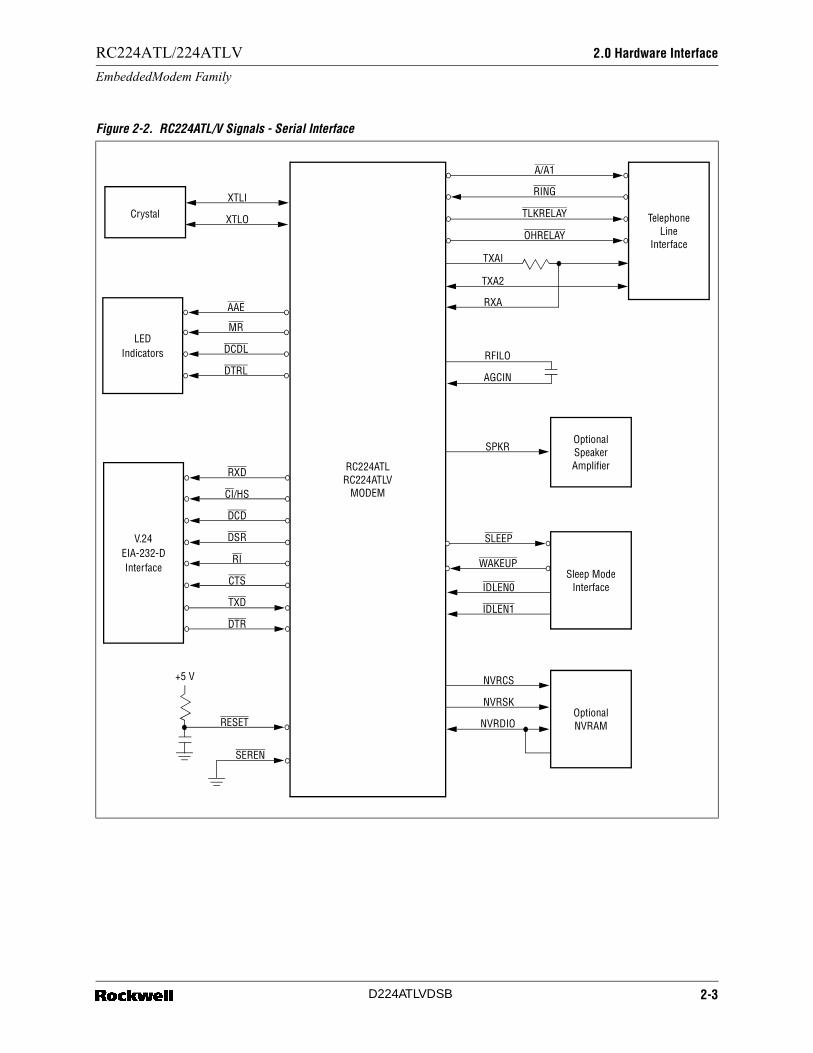
Figure 2-2. RC224ATL/V Signals - Serial Interface . . . . . . . . . . . . . . . . . . . . . . . . . . . . . . . . . . . . . . . . 2-3
Figure 3-1. 68-Pin PLCC Package - Serial . . . . . . . . . . . . . . . . . . . . . . . . . . . . . . . . . . . . . . . . . . . . . . . 3-1
Figure 3-2. 68-Pin PLCC Package - Parallel. . . . . . . . . . . . . . . . . . . . . . . . . . . . . . . . . . . . . . . . . . . . . . 3-2
Figure 3-3. 100-Pin PQFP Package - Serial . . . . . . . . . . . . . . . . . . . . . . . . . . . . . . . . . . . . . . . . . . . . . . 3-3
Figure 3-4. 100-Pin PQFP Package - Parallel. . . . . . . . . . . . . . . . . . . . . . . . . . . . . . . . . . . . . . . . . . . . . 3-4Figure 3-5. NVRAM Timing . . . . . . . . . . . . . . . . . . . . . . . . . . . . . . . . . . . . . . . . . . . . . . . . . . . . . . . . . 3-20Figure 7-1. Timing Waveform . . . . . . . . . . . . . . . . . . . . . . . . . . . . . . . . . . . . . . . . . . . . . . . . . . . . . . . . 7-3Figure 7-2. 68-Pin PLCC . . . . . . . . . . . . . . . . . . . . . . . . . . . . . . . . . . . . . . . . . . . . . . . . . . . . . . . . . . . . 7-7Figure 7-3. 100-Pin PQFP . . . . . . . . . . . . . . . . . . . . . . . . . . . . . . . . . . . . . . . . . . . . . . . . . . . . . . . . . . . 7-9Figure A-1. Serial Interface Design . . . . . . . . . . . . . . . . . . . . . . . . . . . . . . . . . . . . . . . . . . . . . . . . . . . . A-2Figure A-2. Serial Interface Design DAA . . . . . . . . . . . . . . . . . . . . . . . . . . . . . . . . . . . . . . . . . . . . . . . . A-3Figure A-3. Parallel Interface Design . . . . . . . . . . . . . . . . . . . . . . . . . . . . . . . . . . . . . . . . . . . . . . . . . . . A-7Figure A-4. Parallel Interface Design DAA . . . . . . . . . . . . . . . . . . . . . . . . . . . . . . . . . . . . . . . . . . . . . . . A-8
D224ATLVDSB vii

List of Figures RC224ATL/224ATLV
EmbeddedModem Family
viii D224ATLVDSB
RC224ATL/224ATLV List of Tables
EmbeddedModem Family
List of Tables
Table 1-1. Configurations and Rates . . . . . . . . . . . . . . . . . . . . . . . . . . . . . . . . . . . . . . . . . . . . . . . . . . . 1-2Table 1-2. Dial Digits/Tone Pairs . . . . . . . . . . . . . . . . . . . . . . . . . . . . . . . . . . . . . . . . . . . . . . . . . . . . . . 1-4Table 1-3. Current and Power Requirements . . . . . . . . . . . . . . . . . . . . . . . . . . . . . . . . . . . . . . . . . . . . . 1-5Table 2-1. Parallel Interface Registers . . . . . . . . . . . . . . . . . . . . . . . . . . . . . . . . . . . . . . . . . . . . . . . . . . 2-4Table 3-1. RC224ATL/224ATLV 68-Pin PLCC Pin Assignments - Serial Mode . . . . . . . . . . . . . . . . . . . . 3-5Table 3-2. RC224ATLV 68-Pin PLCC Pin Assignments - Parallel Mode . . . . . . . . . . . . . . . . . . . . . . . . . 3-6Table 3-3. RC224ATL/224ATLV 100-Pin PQFP Pin Assignments - Serial . . . . . . . . . . . . . . . . . . . . . . . 3-7Table 3-4. RC224ATL/224ATLV 100-Pin PQFP Pin Assignments - Parallel . . . . . . . . . . . . . . . . . . . . . 3-11Table 3-5. Hardware Interface Signal Definitions . . . . . . . . . . . . . . . . . . . . . . . . . . . . . . . . . . . . . . . . 3-15Table 4-1. Result Codes and Messages . . . . . . . . . . . . . . . . . . . . . . . . . . . . . . . . . . . . . . . . . . . . . . . . 4-1Table 4-2. “AT” Command Set Summary . . . . . . . . . . . . . . . . . . . . . . . . . . . . . . . . . . . . . . . . . . . . . . . 4-2Table 4-3. Fax Command Set Summary . . . . . . . . . . . . . . . . . . . . . . . . . . . . . . . . . . . . . . . . . . . . . . . . 4-8Table 5-1. S Register Description . . . . . . . . . . . . . . . . . . . . . . . . . . . . . . . . . . . . . . . . . . . . . . . . . . . . . 5-1Table 5-2. S Register Summary . . . . . . . . . . . . . . . . . . . . . . . . . . . . . . . . . . . . . . . . . . . . . . . . . . . . . . 5-4Table 6-1. Fax Class 1 Calling Sequence . . . . . . . . . . . . . . . . . . . . . . . . . . . . . . . . . . . . . . . . . . . . . . 6-10Table 6-2. Fax Class 1 Answering Sequence . . . . . . . . . . . . . . . . . . . . . . . . . . . . . . . . . . . . . . . . . . . 6-12Table 6-3. Terminal Called by a 1200 bps Data Modem . . . . . . . . . . . . . . . . . . . . . . . . . . . . . . . . . . . 6-14Table 6-4. Terminal Called by a Fax Machine . . . . . . . . . . . . . . . . . . . . . . . . . . . . . . . . . . . . . . . . . . . . 6-15Table 7-1. Environmental Specifications . . . . . . . . . . . . . . . . . . . . . . . . . . . . . . . . . . . . . . . . . . . . . . . . 7-1Table 7-2. Timing - Host Bus Interface . . . . . . . . . . . . . . . . . . . . . . . . . . . . . . . . . . . . . . . . . . . . . . . . . 7-2Table 7-3. Current and Power Requirements . . . . . . . . . . . . . . . . . . . . . . . . . . . . . . . . . . . . . . . . . . . . . 7-4Table 7-4. Absolute Maximum Ratings . . . . . . . . . . . . . . . . . . . . . . . . . . . . . . . . . . . . . . . . . . . . . . . . . 7-4Table 7-5. Digital Interface Characteristics . . . . . . . . . . . . . . . . . . . . . . . . . . . . . . . . . . . . . . . . . . . . . . 7-5Table 7-6. Analog Interface Characteristics . . . . . . . . . . . . . . . . . . . . . . . . . . . . . . . . . . . . . . . . . . . . . . 7-6Table 7-7. 68-Pin PLCC Dimensions . . . . . . . . . . . . . . . . . . . . . . . . . . . . . . . . . . . . . . . . . . . . . . . . . . . 7-7Table 7-8. 100-Pin PQFP Dimensions . . . . . . . . . . . . . . . . . . . . . . . . . . . . . . . . . . . . . . . . . . . . . . . . . . 7-9Table A-1. Serial Bill of Materials . . . . . . . . . . . . . . . . . . . . . . . . . . . . . . . . . . . . . . . . . . . . . . . . . . . . . A-4Table A-2. Parallel Billing Materials . . . . . . . . . . . . . . . . . . . . . . . . . . . . . . . . . . . . . . . . . . . . . . . . . . . . A-9
D224ATLVDSB ix

List of Tables RC224ATL/224ATLV
EmbeddedModem Family
x D224ATLVDSB

1.0 Functional Description
1.1 Overview
The Rockwell RC224ATL/V is a combination V.22 bis data and Group 3 facsimile (fax) CMOS modem in a single very large scale integration (VLSI) package and is identical to the RC224ATL/V. The RC224ATL/V integrated data/fax modem is available in either a 68-pin plastic leaded chip carrier (PLCC) or a 100-pin plastic quad flat pack (PQFP).
Full error correction (V.42 LAPM, MNP2-4) and data compression (V.42 bis, MNP 5) capabilities can be supported in the RC224ATL/V using the host communication software.
The modem has a selectable parallel or serial interface to the host data terminal equipment (DTE). When parallel mode is selected, a 16C450-compatible interface allows direct connection to a notebook, laptop, or PC-compatible bus without an external universal asynchronous receive/transmit (UART). When serial mode is selected, a CCITT V.24 logic-compatible interface with transistor to transistor logic (TTL) levels is supplied along with indicator outputs.
The RC224ATL/V Designer’s Guide (Order No. 821) provides detailed interface, AT command, and S register information.
1.2 Technical Specifications
1.2.1 General
The RC224ATL/V modem is a full-featured, self-contained data/fax solution. No external microcontroller for data or fax control functions is required. Dialing, call progress, and telephone line interface functions are fully supported and controlled through the AT command set.
Data modes perform complete handshake and data rate negotiations. All tone and pattern detection required by the applicable CCITT or Bell standard are supported.
Fax modes support Group 3 fax requirements. Fax data and fax control (V.21 300 bps), performed by the modem, is controlled and monitored through the fax
1-1 D224ATLVDSB

1.0 Functional Description 1.2 Technical Specifications
RC224ATL/224ATLV
EmbeddedModem Family
EIA-578 Class 1 command interface. Full HDLC formatting, flag insertion/deletion, and CRC generation/checking is provided.
Both transmit and receive fax data is buffered within the modem. Fax data transfer to and from the DTE is flow controlled by XON/XOFF.
1.2.2 Configurations and Rates
The supported modem configurations and signaling rates are listed in Table 1-1. In data modes with serial interface selected, DTE rate offsets of +1%, -2.5% are accommodated by adding/deleting stop bits as required. In fax modes, the DTE rate is 19200 bps.
Table 1-1. Configurations and Rates
Configuration Modulation Transmitter CarrierFrequency (Hz) ±0.01%
Data Rate (bps)
Baud(Symbols/Sec.)
Bits Per Symbol
Constellation Points
Data ModeV.22bisV.22Bell 212ABell 103
QAMDPSKDPSKFSK
Answer240024002400
2225 M2025 S
Originate120012001200
1270 M1070 S
240012001200300
600600600300
4221
16441
Fax ModeV.29
V.27ter
V.21
QAMQAMDPSKDPSKFSK
ReceiveN/AN/A
18001800
1650 M1850 S
Transmit1700170018001800
1650 M1850 S
9600720048002400300
2400240016001200300
43321
168841
Notes:
Legend:QAM = Quadrature Amplitude ModulationDPSK = Differential Phase Shift KeyingFSK = Frequency Shift KeyingM = Mark conditionS = Space ConditionN/A = Not Applicable
1-2 D224ATLVDSB
1.0 Functional Description
1.2 Technical Specifications
RC224ATL/224ATLV
EmbeddedModem Family
1.2.3 Operation
Modem operation is controlled by AT commands, fax service class 1 commands, and supporting S registers.
1.2.3.1 Data Modes Data rate selection is determined by the speed of the originating and answering modems:
1.2.3.2 Fax Modes Fax modes are negotiated as defined in T.30 and are implemented by AT+F commands. The AT+FCLASS=1 command causes entry into the fax mode from the data mode. Most other fax class 1 commands, which start with the AT+F prefix, are valid only in the fax mode. All data commands are valid in the fax mode except A/, On, &Tn, and the escape sequence (+++). The AT+FCLASS=0 command terminates the fax mode and causes entry into the data mode.
1.2.4 Data/Fax Auto Answering
The modem can automatically determine if the incoming call is from a data or fax modem, make the appropriate connection, and inform the DTE of the connection type.
1.2.5 Data Modulation
The data modulation conforms to V.29, V.27 ter, V.22 bis, V.22, V.21, Bell 212A, or Bell 103, depending on the selected configuration. Transmitter and receiver spectrum shaping is provided in accordance with the applicable standard.
1.2.6 Equalization
Automatic adaptive equalization as well as fixed compromised equalization is provided to compensate for line distortions and to minimize the effects of intersymbol interference.
1.2.7 Scrambler/Descrambler
The modem incorporates a self-synchronizing scrambler/descrambler satisfying the applicable CCITT or Bell requirements.
Originate Modem Rate (bps)
Connect Speed Based on Answer Modem Rate (bps)
300 1200 2400
300 300 300 300
1200 300 1200 1200
2400 300 1200 2400
1-3 D224ATLVDSB

1.0 Functional Description 1.2 Technical Specifications
RC224ATL/224ATLV
EmbeddedModem Family
1.2.8 Transmit Level
The transmit level is -10 dBm ±1 dB (at TIP and RING) and can be obtained using the circuits shown in Appendix A. Carrier and dual tone multi-frequency (DTMF) transmit levels can be further attenuated using AT%Ln + AT%Dn commands, respectively. If a higher transmit level is required, an external op amp can be added.
1.2.9 Transmit Tones
Answer Tone An answer tone of 2100 Hz (V.22 bis, V.22, or T.30) or 2225 Hz (Bell 212A or 103) is generated.
Guard Tone An 1800 Hz guard tone can be generated in all data modes.
Calling Tone An 1100 Hz (0.5 seconds on, 3 seconds off) calling tone (T.30) is generated in the originate fax mode.
1.2.10 Receive Level
The receiver satisfies performance requirements for a received signal from -9 dBm to -43 dBm. The carrier detect is ON at -43 dBm and OFF at -48 dBm with a minimum of 2 dB hysteresis.
1.2.11 Receiver Tracking
The modem can accommodate carrier frequency offset up to ±7 Hz, and a transmit timing error of ±0.01% (V.22 bis or V.27 ter) or ±0.02% (V.22 or Bell 212A).
DTMF Dialing Standard DTMF tones (digits 0-9, A, B, C, D, *, and #) or pulses (digits 0-9) can be generated. See Table 1-2.
Ring Detection RING signal is detected from valid high to low transitions on the RING input line at frequencies of 15.3 Hz to 63 Hz. A RING is valid if the RING ON time is greater than 0.125 seconds and is followed by a RING OFF time greater than 0.5 seconds.
Table 1-2. Dial Digits/Tone Pairs (1 of 2)
Dial Digit Tone 1Frequency (Hz)
Tone 2Frequency (Hz)
0 941 1336
1 697 1209
2 697 1336
3 697 1477
4 770 1209
5 770 1336
1-4 D224ATLVDSB
1.0 Functional Description
1.2 Technical Specifications
RC224ATL/224ATLV
EmbeddedModem Family
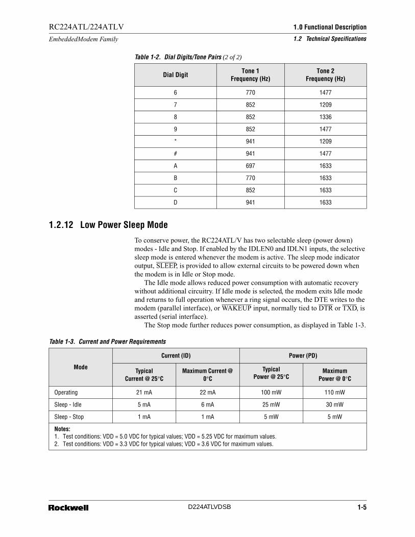
1.2.12 Low Power Sleep Mode
To conserve power, the RC224ATL/V has two selectable sleep (power down) modes - Idle and Stop. If enabled by the IDLEN0 and IDLN1 inputs, the selective sleep mode is entered whenever the modem is active. The sleep mode indicator output, SLEEP, is provided to allow external circuits to be powered down when the modem is in Idle or Stop mode.
The Idle mode allows reduced power consumption with automatic recovery without additional circuitry. If Idle mode is selected, the modem exits Idle mode and returns to full operation whenever a ring signal occurs, the DTE writes to the modem (parallel interface), or WAKEUP input, normally tied to DTR or TXD, is asserted (serial interface).
The Stop mode further reduces power consumption, as displayed in Table 1-3.
6 770 1477
7 852 1209
8 852 1336
9 852 1477
* 941 1209
# 941 1477
A 697 1633
B 770 1633
C 852 1633
D 941 1633
Table 1-2. Dial Digits/Tone Pairs (2 of 2)
Dial Digit Tone 1Frequency (Hz)
Tone 2Frequency (Hz)
Table 1-3. Current and Power Requirements
Mode
Current (ID) Power (PD)
TypicalCurrent @ 25°C
Maximum Current @ 0°C
TypicalPower @ 25°C
MaximumPower @ 0°C
Operating 21 mA 22 mA 100 mW 110 mW
Sleep - Idle 5 mA 6 mA 25 mW 30 mW
Sleep - Stop 1 mA 1 mA 5 mW 5 mW
Notes:1. Test conditions: VDD = 5.0 VDC for typical values; VDD = 5.25 VDC for maximum values.2. Test conditions: VDD = 3.3 VDC for typical values; VDD = 3.6 VDC for maximum values.
1-5 D224ATLVDSB

1.0 Functional Description 1.3 Low Power Modes
RC224ATL/224ATLV
EmbeddedModem Family
1.3 Low Power Modes
1.3.1 Sleep Mode
Entry The modem will enter the low power sleep mode when no line connection exists and no host activity occurs for the period of time specified in the S24 register. All EmbeddedModem circuits are turned off except the internal micro controller unit (MCU) clock circuitry in order to consume lower power but are able to immediately wake up and resume normal operation.
Wake-up - ParallelInterface Configuration
Wake-up occurs when a ring signal occurs, or the host write to the modem.
Wake-up - SerialInterface Configuration
Wake-up occurs when a ring signal occurs, or the DTE sends a character to the modem.
1-6 D224ATLVDSB

2.0 Hardware Interface
The RC224ATL/V hardware interface signals are shown for the parallel interface in Figure 2-1, and for the serial interface in Figure 2-2.
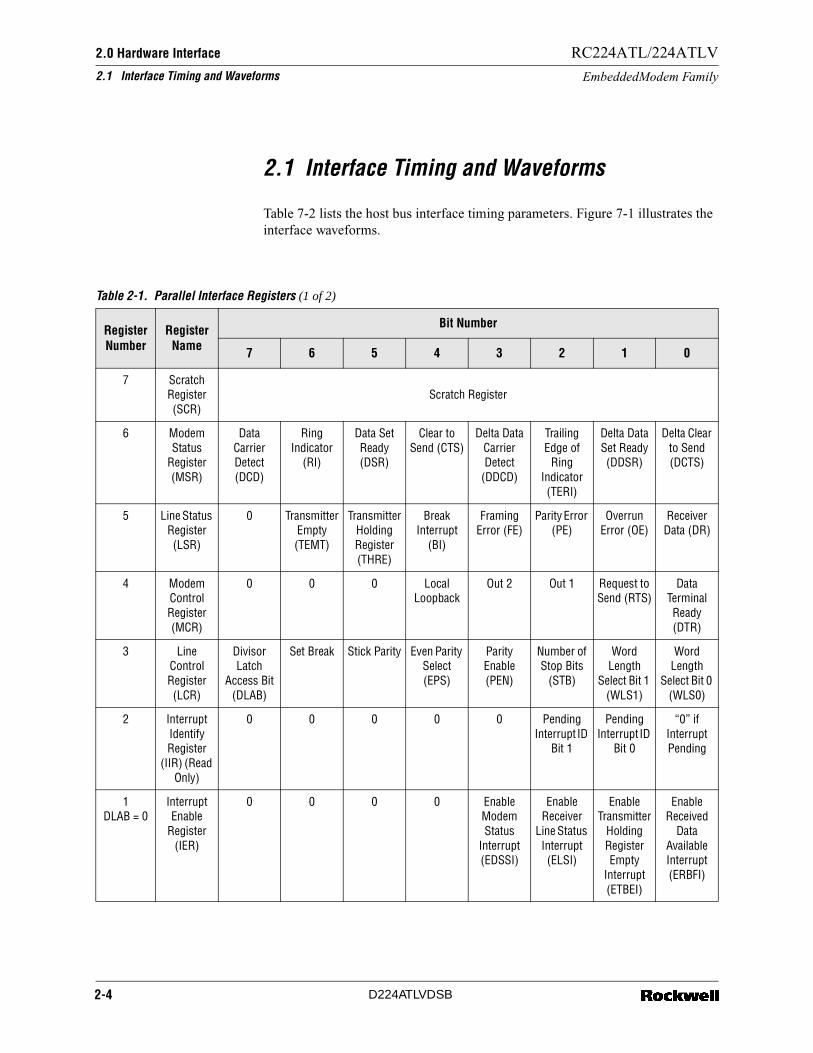
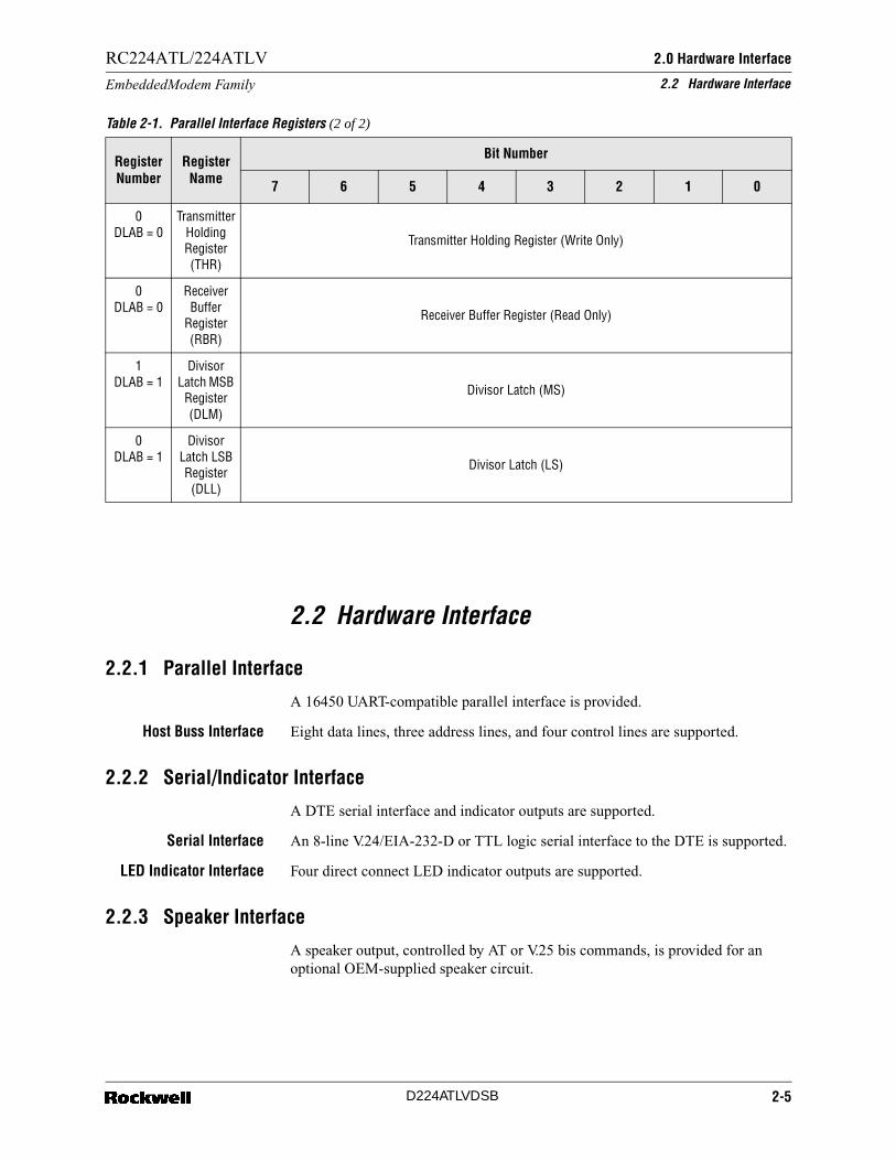
The RC224ATL/V hardware interface signals are described in Table 3-5.The parallel interface registers are identified in Table 2-1.
2-1 D224ATLVDSB

2.0 Hardware Interface
RC224ATL/224ATLV
EmbeddedModem Family
Figure 2-1. RC224ATL/V Signals - Parallel Interface
HostComputer
Parallel BUS
Crystal
HDIS
HCS
HRD
HWT
HINT
HA0
HA1
HA2
HD0
HD1
HD2
HD3
HD4
HD5
HD6
HD7
RESET
XTLI
XTLO
RC224ATLRC224ATLV
MODEM
Optional
NVRCS
NVRSK
NVRAMNVRDIO
RFILO
AGCIN
Sleep ModeInterface
SLEEP
IDLEN0
IDLEN1
OptionalSpeakerAmplifier
SPKR
TelephoneLine
Interface
A/A1
RING
TLKRELAY
OHRELAY
TXAI
TXA2
RXA
2-2 D224ATLVDSB
2.0 Hardware InterfaceRC224ATL/224ATLV
EmbeddedModem Family
Figure 2-2. RC224ATL/V Signals - Serial Interface
V.24EIA-232-DInterface
Crystal
MR
DCDL
DTRL
RXD
CI/HS
DCD
DSR
RI
CTS
TXD
DTR
RESET
XTLI
XTLO
RC224ATLRC224ATLV
MODEM
Optional
NVRCS
NVRSK
NVRAMNVRDIO
RFILO
AGCIN
Sleep ModeInterface
SLEEP
IDLEN0
IDLEN1
OptionalSpeakerAmplifier
SPKR
TelephoneLine
Interface
A/A1
RING
TLKRELAY
OHRELAY
TXAI
TXA2
RXA
LEDIndicators
WAKEUP
AAE
SEREN
+5 V
2-3 D224ATLVDSB
2.0 Hardware Interface 2.1 Interface Timing and Waveforms
RC224ATL/224ATLV
EmbeddedModem Family
2.1 Interface Timing and Waveforms
Table 7-2 lists the host bus interface timing parameters. Figure 7-1 illustrates the interface waveforms.
Table 2-1. Parallel Interface Registers (1 of 2)
Register Number
Register Name
Bit Number
7 6 5 4 3 2 1 0
7 Scratch Register (SCR)
Scratch Register
6 Modem Status
Register (MSR)
Data Carrier Detect (DCD)
Ring Indicator
(RI)
Data Set Ready (DSR)
Clear to Send (CTS)
Delta Data Carrier Detect
(DDCD)
Trailing Edge of
Ring Indicator (TERI)
Delta Data Set Ready (DDSR)
Delta Clear to Send (DCTS)
5 Line Status Register (LSR)
0 Transmitter Empty (TEMT)
Transmitter Holding Register (THRE)
Break Interrupt
(BI)
Framing Error (FE)
Parity Error (PE)
Overrun Error (OE)
Receiver Data (DR)
4 Modem Control Register (MCR)
0 0 0 Local Loopback
Out 2 Out 1 Request to Send (RTS)
Data Terminal Ready (DTR)
3 Line Control Register (LCR)
Divisor Latch
Access Bit (DLAB)
Set Break Stick Parity Even Parity Select (EPS)
Parity Enable (PEN)
Number of Stop Bits
(STB)
Word Length
Select Bit 1 (WLS1)
Word Length
Select Bit 0 (WLS0)
2 Interrupt Identify Register
(IIR) (Read Only)
0 0 0 0 0 Pending Interrupt ID
Bit 1
Pending Interrupt ID
Bit 0
“0” if Interrupt Pending
1 DLAB = 0
Interrupt Enable
Register (IER)
0 0 0 0 Enable Modem Status
Interrupt (EDSSI)
Enable Receiver
Line Status Interrupt (ELSI)
Enable Transmitter
Holding Register Empty
Interrupt (ETBEI)
Enable Received
Data Available Interrupt (ERBFI)
2-4 D224ATLVDSB
2.0 Hardware Interface
2.2 Hardware Interface
RC224ATL/224ATLV
EmbeddedModem Family
2.2 Hardware Interface
2.2.1 Parallel Interface
A 16450 UART-compatible parallel interface is provided.
Host Buss Interface Eight data lines, three address lines, and four control lines are supported.
2.2.2 Serial/Indicator Interface
A DTE serial interface and indicator outputs are supported.
Serial Interface An 8-line V.24/EIA-232-D or TTL logic serial interface to the DTE is supported.
LED Indicator Interface Four direct connect LED indicator outputs are supported.
2.2.3 Speaker Interface
A speaker output, controlled by AT or V.25 bis commands, is provided for an optional OEM-supplied speaker circuit.
0 DLAB = 0
Transmitter Holding Register (THR)
Transmitter Holding Register (Write Only)
0 DLAB = 0
Receiver Buffer
Register (RBR)
Receiver Buffer Register (Read Only)
1 DLAB = 1
Divisor Latch MSB
Register (DLM)
Divisor Latch (MS)
0 DLAB = 1
Divisor Latch LSB Register
(DLL)
Divisor Latch (LS)
Table 2-1. Parallel Interface Registers (2 of 2)
Register Number
Register Name
Bit Number
7 6 5 4 3 2 1 0
2-5 D224ATLVDSB
2.0 Hardware Interface 2.3 Low Power Modes
RC224ATL/224ATLV
EmbeddedModem Family
2.2.4 Line Interface
The EmbeddedModem connects to the line interface circuitry via a receive analog input, two transmit analog outputs, and a ring signal input.
The EmbeddedModem provides three relay control outputs to the line interface. These outputs may be used to control relays such as off-hook, A/A1, and talk/data.
2.3 Low Power Modes
2.3.1 Sleep Mode
Entry The modem will enter the low power sleep mode when no line connection exists and no host activity occurs for the period of time specified in the S24 register. All EmbeddedModem circuits are turned off except the internal MCU clock circuitry in order to consume lower power but are able to immediately wake up and resume normal operation.
Wake-up - ParallelInterface Configuration
Wake-up occurs when a ring signal occurs, or the host writes to the modem.
Wake-up - SerialInterface Configuration
Wake-up occurs when a ring signal occurs, or the DTE sends a character to the modem.
2.4 Additional Information
Additional information is described in the RC224ATL/V Modem Designer’s Guide (Order No. 821).
2-6 D224ATLVDSB

3.0 Pin Descriptions
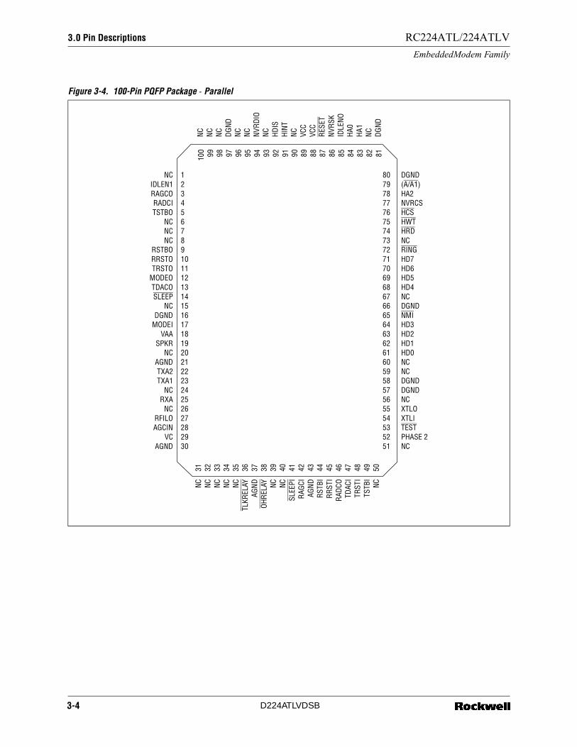
The RC224ATL/V 68-pin PLCC pinout diagrams are provided as Figure 3-1 and Figure 3-2 for serial and parallel interface implementations, respectively. The 100-pin PQFP pinout diagrams are provided as Figure 3-3 and Figure 3-4 for serial and parallel interface implementations, respectively.
RC224ATL/V 68-pin PLCC pin assignments are given in Table 3-1 and Table 3-2 for serial and parallel interface implementations, respectively. The 100-pin PQFP pinout diagrams are provided as Table 3-3 and Table 3-4 for serial and parallel interface implementations, respectively.
Figure 3-1. 68-Pin PLCC Package - Serial
AAE DTRL
NC RXD
RESET VCC
NVRSK NC NC
TXD DTR
IDLEN1 RAGCO RADCI TSTBO RSTBO RRSTO
10 11 12 13 14 15 16 17 18 19 20 21 22 23 24 25 26
DGND1 XTLO XTLI TEST φ2 SLEEP SPKR VAA MODEI TSTBI TRSTI TDACI RADCO RRSTI NC RSTBI NC
60 59 58 57 56 55 54 53 52 51 50 49 48 47 46 45 44
A/A
1 N
VR
DIO
N
VR
CS
W
AK
EU
P
SE
RE
N
NC
R
ING
ID
LEN
0 D
CD
L R
I M
R
NM
I C
I/HS
D
CD
C
TS
D
SR
D
GN
D2
9 8 7 6 5 4 3 2 1 68
67
66
65
64
63
62
61
27
28
29
30
31
32
33
34
35
36
37
38
39
40
41
42
43
TR
ST
O
MO
DE
O
TD
AC
O
NC
T
XA
2 T
XA
1 R
XA
R
FIL
O
AG
CIN
V
C
NC
T
LKR
ELA
Y
AG
ND
O
HR
ELA
Y
NC
S
LEE
PI
RA
GC
I
3-1 D224ATLVDSB

3.0 Pin Descriptions
RC224ATL/224ATLV
EmbeddedModem Family
Figure 3-2. 68-Pin PLCC Package - Parallel
HA1 HA0
IDLEN0NVRSK RESET
VCC HINT HDIS
NC NVRDIO
NC IDLEN1 RAGCO RADCI TSTBO RSTBO RRSTO
10 11 12 13 14 15 16 17 18 19 20 21 22 23 24 25 26
DGND1 XTLO XTLI TEST φ2 SLEEP SPKR VAA MODEI TSTBI TRSTI TDACI RADCO RRSTI NC RSTBI NC
60 59 58 57 56 55 54 53 52 51 50 49 48 47 46 45 44
A/A
1 H
A2
NV
RC
S
HC
S
HW
T
HR
D
RIN
G
HD
7 H
D6
HD
5 H
D4
NM
I H
D3
HD
2 H
D1
HD
0 D
GN
D2
9 8 7 6 5 4 3 2 1 68
67
66
65
64
63
62
61
27
28
29
30
31
32
33
34
35
36
37
38
39
40
41
42
43
TR
ST
O
MO
DE
O
TD
AC
O
NC
T
XA
2 T
XA
1 R
XA
R
FIL
O
AG
CIN
V
C
NC
T
LKR
ELA
Y
AG
ND
O
HR
ELA
Y
NC
S
LEE
PI
RA
GC
I
3-2 D224ATLVDSB

3.0 Pin DescriptionsRC224ATL/224ATLV
EmbeddedModem Family
Figure 3-3. 100-Pin PQFP Package - Serial
100 99 98 97 96 95 94 93 92 91 90 89 88 87 86 85 84 83 82 81
31 32 33 34 35 36 37 38 39 40 41 42 43 44 45 46 47 48 49 50
NC
NC
NC
NC
NC
TLKR
ELAY
AGND
OH
RELA
YN
CN
CSL
EEPI
RAG
CIAG
ND
RST
BIRR
STI
RADC
OTD
ACI
TRST
ITS
TBI
NC
DTRIDLEN1RAGCORADCITSTBO
NCNCNC
RSTBORRSTOTRSTO
MODEOTDACOSLEEP
NCDGND
MODEIVAA
SPKRNC
AGNDTXA2TXA1
NCRXA
NCRFILOAGCIN
VCAGND
123456789101112131415161718192021222324252627282930
DGND(A/A1)NVRDIONVRCSWAKEUPSERENNCNCRINGIDLENODCDLRIMRNCDGNDNMICI/HSDCDCTSDSRNCNCDGNDDGNDNCXTLOXTLITESTPHASE 2NC
807978777675747372717069686766656463626160595857565554535251
NC
NC
NC
DG
ND
NC
NC
TXD
NC
NC
NVRS
KN
CVC
CVC
CR
ESET
RXD
NC
DTR
LAA
EN
CD
GN
D
3-3 D224ATLVDSB
3.0 Pin Descriptions
RC224ATL/224ATLV
EmbeddedModem Family
Figure 3-4. 100-Pin PQFP Package - Parallel
100 99 98 97 96 95 94 93 92 91 90 89 88 87 86 85 84 83 82 81
31 32 33 34 35 36 37 38 39 40 41 42 43 44 45 46 47 48 49 50
NC NC NC NC NCTL
KREL
AYAG
NDO
HREL
AY NC NCSL
EEPI
RAGC
IAG
NDRS
TBI
RRS
TIRA
DCO
TDAC
ITR
STI
TSTB
INC
NCIDLEN1RAGCORADCITSTBO
NCNCNC
RSTBORRSTOTRSTO
MODEOTDACOSLEEP
NCDGND
MODEIVAA
SPKRNC
AGNDTXA2TXA1
NCRXA
NCRFILOAGCIN
VCAGND
123456789101112131415161718192021222324252627282930
DGND(A/A1)HA2NVRCSHCSHWTHRDNCRINGHD7HD6HD5HD4NCDGNDNMIHD3HD2HD1HD0NCNCDGNDDGNDNCXTLOXTLITESTPHASE 2NC
807978777675747372717069686766656463626160595857565554535251
NC
NC
NC
DG
NDN
CN
CNV
RDIO
NC
HD
ISH
INT
NC
VCC
VCC
RES
ETNV
RSK
IDLE
NO
HA0
HA1
NC
DG
ND
3-4 D224ATLVDSB
3.0 Pin DescriptionsRC224ATL/224ATLV
EmbeddedModem Family
Table 3-1. RC224ATL/224ATLV 68-Pin PLCC Pin Assignments - Serial Mode
Pin Number Signal Label I/O Type Pin
Number Signal Label I/O Type
1 DCDL D0 35 AGCIN
2 IDLEN0 DI 36 VC
3 RING DI 37 NC
4 NC 38 TLKRELAY OD
5 SEREN DI 39 AGND
6 WAKEUP DI 40 OHRELAY OD
7 NVRCS DO 41 NC
8 NVRDIO DI 42 SLEEPI DI
9 A/A1 DO 43 RAGCI MI TO RAGCO
10 AAE DO 44 NC
11 DTRL DO 45 RSTBI MI TO RSTBO
12 NC 46 NC
13 RXD DO 47 RRSTI MI TO RRSTO
14 RESET DI 48 RADCO RADCO
15 VCC 49 TDACI MI TO TADCO
16 NVRSK DO 50 TRSTI MI TO TRSTO
17 NC 51 TSTBI MI TO TSTBO
18 NC 52 MODEI MI TO MODEO
19 TXD DI 53 VAA
20 DTR DI 54 SPKR O(DF)
21 IDLEN1 DI 55 SLEEP DO
22 RAGCO MI TO RAGCI 56 φ2 DO
23 RADCI MI TO RADCO 57 TEST DI 4.7K TO VCC
24 TSTBO MI TO TSTBI 58 XTLI IE
25 RSTBO MI TO RSTBI 59 XTLO OE
26 RRSTO MI TO RRSTI 60 DGND1
27 TRSTO MI TO TRSTI 61 DGND2
28 MODEO MI TO MODEI 62 DSR DO
29 TDACO MI TO TDACI 63 CTS DO
30 NC 64 DCD DO
31 TXA2 O (DD) 65 CI/HS DO
32 TXA1 O(DD) 66 NMI DI
33 RXA I(DA) 67 MR DO
34 RFILO 68 RI DO
3-5 D224ATLVDSB
3.0 Pin Descriptions
RC224ATL/224ATLV
EmbeddedModem Family
Table 3-2. RC224ATLV 68-Pin PLCC Pin Assignments - Parallel Mode
Pin Number Signal Label I/O Type Pin
Number Signal Label I/O Type
1 HD6 DIO 35 AGCIN
2 HD7 DIO 36 VC
3 RING DI 37 NC
4 HRD DI 38 TLKRELAY OD
5 HWT DI 39 AGND
6 HCS DI 40 OHRELAY OD
7 NVRCS DO 41 NC
8 HA2 DI 42 SLEEPI DI
9 A/A1 DO 43 RAGCI MI TO RAGCO
10 HA1 DI 44 NC
11 HA0 DI 45 RSTBI MI TO RSTBO
12 IDLEN0 46 NC
13 NVRSK DO 47 RRSTI MI TO RRSTO
14 RESET DI 48 RADCO RADCO
15 VCC 49 TDACI MI TO TADCO
16 HINT DO 50 TRSTI MI TO TRSTO
17 HDIS DO 51 TSTBI MI TO TSTBO
18 NC 52 MODEI MI TO MODEO
19 NVRDIO DIO 53 VAA
20 NC 54 SPKR O(DF)
21 IDLEN1 DI 55 SLEEP OA
22 RAGCO MI TO RAGCI 56 φ2 OA
23 RADCI MI TO RADCO 57 TEST 4.7k TO VCC
24 TSTBO MI TO TSTBI 58 XTLI IE
25 RSTBO MI TO RSTBI 59 XTLO OE
26 RRSTO MI TO RRSTI 60 DGND1
27 TRSTO MI TO TRSTI 61 DGND2
28 MODEO MI TO MODEI 62 HD0 DIO
29 TDACO MI TO TDACI 63 HD1 DIO
30 NC 64 HD2 DIO
31 TXA2 O (DD) 65 HD3 DIO
32 TXA1 O(DD) 66 NMI DI
33 RXA I(DA) 67 HD4 DIO
34 RFILO 68 HD5 DIO
3-6 D224ATLVDSB

3.0 Pin DescriptionsRC224ATL/224ATLV
EmbeddedModem Family
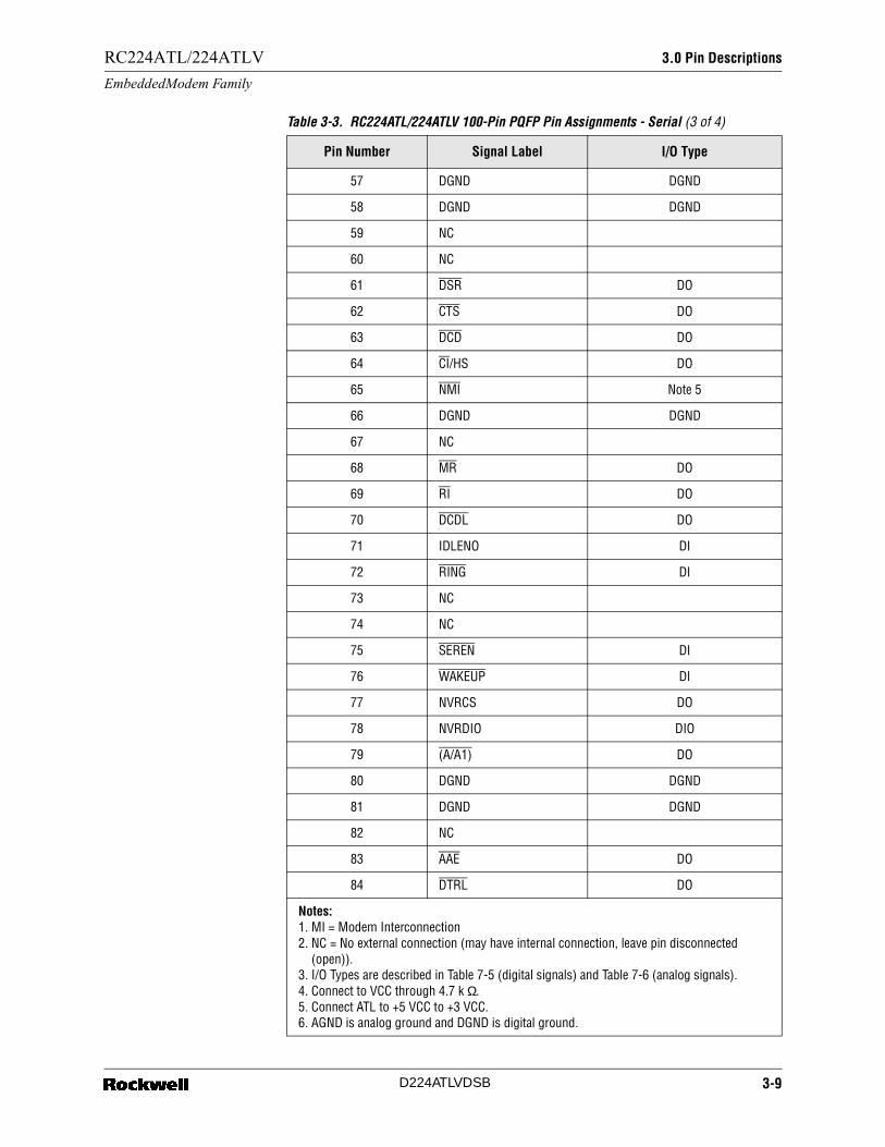
Table 3-3. RC224ATL/224ATLV 100-Pin PQFP Pin Assignments - Serial (1 of 4)
Pin Number Signal Label I/O Type
1 DTR DI
2 IDLEN1 DI
3 RAGCO MI to RAGCI
4 RADCI MI to RADCO
5 TSTBO MI to TSTBI
6 NC
7 NC
8 NC
9 RSTBO MI to RSTBI
10 RRSTO MI to RRSTI
11 TRSTO MI to TRSTI
12 MODEO MI to MODEI
13 TDACO MI to TDACI
14 SLEEP DO
15 NC
16 DGND DGND
17 MODEI MI to MODEO
18 VAA
19 SPKR O(DF)
20 NC
21 AGND AGND
22 TXA2 O(DD)
23 TXA1 O(DD)
24 NC
25 RXA I(DA)
26 NC
27 RFILO
28 AGCIN
Notes: 1. MI = Modem Interconnection2. NC = No external connection (may have internal connection, leave pin disconnected
(open)).3. I/O Types are described in Table 7-5 (digital signals) and Table 7-6 (analog signals).4. Connect to VCC through 4.7 k Ω.5. Connect ATL to +5 VCC to +3 VCC.6. AGND is analog ground and DGND is digital ground.
3-7 D224ATLVDSB
3.0 Pin Descriptions
RC224ATL/224ATLV
EmbeddedModem Family
29 VC
30 AGND AGND
31 NC
32 NC
33 NC
34 NC
35 NC
36 TLKRELAY OD
37 AGND AGND
38 OHRELAY OD
39 NC
40 NC
41 SLEEPI DI
42 RAGCI MI to RAGCO
43 AGND AGND
44 RSTBI MI to RSTBO
45 RRSTI MI to RRSTO
46 RADCO MI to RADCI
47 TDACI MI to TDACO
48 TRSTI MI to TRSTO
49 TSTBI MI to TSTBO
50 NC
51 NC
52 PHASE 2 DO
53 TEST Note 4
54 XTLI IE
55 XTLO OE
56 NC
Table 3-3. RC224ATL/224ATLV 100-Pin PQFP Pin Assignments - Serial (2 of 4)
Pin Number Signal Label I/O Type
Notes: 1. MI = Modem Interconnection2. NC = No external connection (may have internal connection, leave pin disconnected
(open)).3. I/O Types are described in Table 7-5 (digital signals) and Table 7-6 (analog signals).4. Connect to VCC through 4.7 k Ω.5. Connect ATL to +5 VCC to +3 VCC.6. AGND is analog ground and DGND is digital ground.
3-8 D224ATLVDSB
3.0 Pin DescriptionsRC224ATL/224ATLV
EmbeddedModem Family
57 DGND DGND
58 DGND DGND
59 NC
60 NC
61 DSR DO
62 CTS DO
63 DCD DO
64 CI/HS DO
65 NMI Note 5
66 DGND DGND
67 NC
68 MR DO
69 RI DO
70 DCDL DO
71 IDLENO DI
72 RING DI
73 NC
74 NC
75 SEREN DI
76 WAKEUP DI
77 NVRCS DO
78 NVRDIO DIO
79 (A/A1) DO
80 DGND DGND
81 DGND DGND
82 NC
83 AAE DO
84 DTRL DO
Table 3-3. RC224ATL/224ATLV 100-Pin PQFP Pin Assignments - Serial (3 of 4)
Pin Number Signal Label I/O Type
Notes: 1. MI = Modem Interconnection2. NC = No external connection (may have internal connection, leave pin disconnected
(open)).3. I/O Types are described in Table 7-5 (digital signals) and Table 7-6 (analog signals).4. Connect to VCC through 4.7 k Ω.5. Connect ATL to +5 VCC to +3 VCC.6. AGND is analog ground and DGND is digital ground.
3-9 D224ATLVDSB
3.0 Pin Descriptions
RC224ATL/224ATLV
EmbeddedModem Family
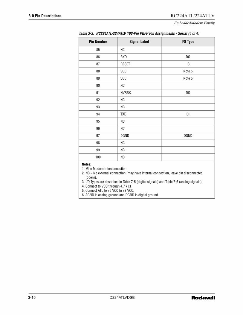
85 NC
86 RXD DO
87 RESET IC
88 VCC Note 5
89 VCC Note 5
90 NC
91 NVRSK DO
92 NC
93 NC
94 TXD DI
95 NC
96 NC
97 DGND DGND
98 NC
99 NC
100 NC
Table 3-3. RC224ATL/224ATLV 100-Pin PQFP Pin Assignments - Serial (4 of 4)
Pin Number Signal Label I/O Type
Notes: 1. MI = Modem Interconnection2. NC = No external connection (may have internal connection, leave pin disconnected
(open)).3. I/O Types are described in Table 7-5 (digital signals) and Table 7-6 (analog signals).4. Connect to VCC through 4.7 k Ω.5. Connect ATL to +5 VCC to +3 VCC.6. AGND is analog ground and DGND is digital ground.
3-10 D224ATLVDSB

3.0 Pin DescriptionsRC224ATL/224ATLV
EmbeddedModem Family
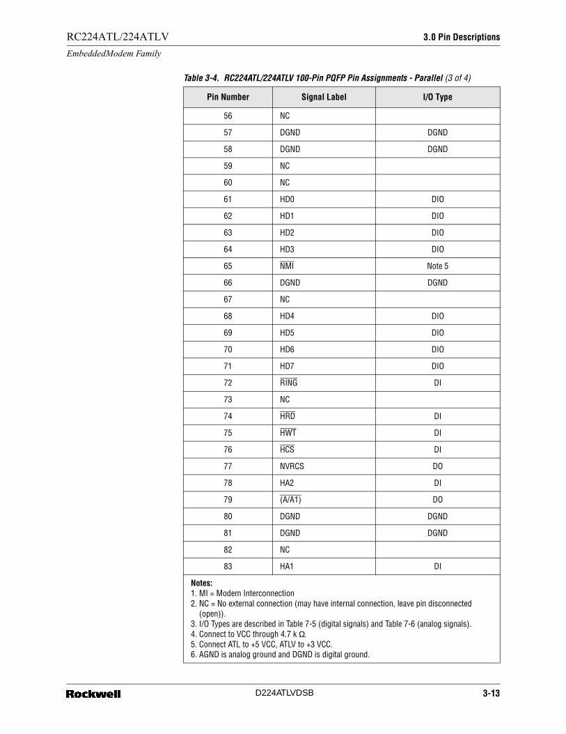
Table 3-4. RC224ATL/224ATLV 100-Pin PQFP Pin Assignments - Parallel (1 of 4)
Pin Number Signal Label I/O Type
1 NC
2 IDLEN1 DI
3 RAGCO MI to RAGCI
4 RADCI MI to RADCO
5 TSTBO MI to TSTBI
6 NC
7 NC
8 NC
9 RSTBO MI to RSTBI
10 RRSTO MI to RRSTI
11 TRSTO MI to TRSTI
12 MODEO MI to MODEI
13 TDACO MI to TDACI
14 SLEEP DO
15 NC
16 DGND DGND
17 MODEI MI to MODEO
18 VAA
19 SPKR O(DF)
20 NC
21 AGND AGND
22 TXA2 O(DD)
23 TXA1 O(DD)
24 NC
25 RXA I(DA)
26 NC
27 RFILO
Notes: 1. MI = Modem Interconnection2. NC = No external connection (may have internal connection, leave pin disconnected
(open)).3. I/O Types are described in Table 7-5 (digital signals) and Table 7-6 (analog signals).4. Connect to VCC through 4.7 k Ω.5. Connect ATL to +5 VCC, ATLV to +3 VCC.6. AGND is analog ground and DGND is digital ground.
3-11 D224ATLVDSB

3.0 Pin Descriptions
RC224ATL/224ATLV
EmbeddedModem Family
28 AGCIN
29 VC
30 AGND AGND
31 NC
32 NC
33 NC
34 NC
35 NC
36 TLKRELAY DO
37 AGND AGND
38 OHRELAY DO
39 NC
40 NC
41 SLEEPI DI
42 RAGCI MI to RAGCO
43 AGND AGND
44 RSTBI MI to RSTBO
45 RRSTI MI to RRSTO
46 RADCO MI to RADCI
47 TDACI MI to TDACO
48 TRSTI MI to TRSTO
49 TSTBI MI to TSTBO
50 NC
51 NC
52 PHASE 2 DI
53 TEST Note 4
54 XTLI IE
55 XTLO OE
Table 3-4. RC224ATL/224ATLV 100-Pin PQFP Pin Assignments - Parallel (2 of 4)
Pin Number Signal Label I/O Type
Notes: 1. MI = Modem Interconnection2. NC = No external connection (may have internal connection, leave pin disconnected
(open)).3. I/O Types are described in Table 7-5 (digital signals) and Table 7-6 (analog signals).4. Connect to VCC through 4.7 k Ω.5. Connect ATL to +5 VCC, ATLV to +3 VCC.6. AGND is analog ground and DGND is digital ground.
3-12 D224ATLVDSB
3.0 Pin DescriptionsRC224ATL/224ATLV
EmbeddedModem Family
56 NC
57 DGND DGND
58 DGND DGND
59 NC
60 NC
61 HD0 DIO
62 HD1 DIO
63 HD2 DIO
64 HD3 DIO
65 NMI Note 5
66 DGND DGND
67 NC
68 HD4 DIO
69 HD5 DIO
70 HD6 DIO
71 HD7 DIO
72 RING DI
73 NC
74 HRD DI
75 HWT DI
76 HCS DI
77 NVRCS DO
78 HA2 DI
79 (A/A1) DO
80 DGND DGND
81 DGND DGND
82 NC
83 HA1 DI
Table 3-4. RC224ATL/224ATLV 100-Pin PQFP Pin Assignments - Parallel (3 of 4)
Pin Number Signal Label I/O Type
Notes: 1. MI = Modem Interconnection2. NC = No external connection (may have internal connection, leave pin disconnected
(open)).3. I/O Types are described in Table 7-5 (digital signals) and Table 7-6 (analog signals).4. Connect to VCC through 4.7 k Ω.5. Connect ATL to +5 VCC, ATLV to +3 VCC.6. AGND is analog ground and DGND is digital ground.
3-13 D224ATLVDSB

3.0 Pin Descriptions
RC224ATL/224ATLV
EmbeddedModem Family
84 HA0 DI
85 IDLENO DI
86 NVRSK DO
87 RESET IC
88 VCC Note 5
89 VCC Note 5
90 NC
91 HINT DO
92 HDIS DO
93 NC
94 NVRDIO DIO
95 NC
96 NC
97 DGND DGND
98 NC
99 NC
100 NC
Table 3-4. RC224ATL/224ATLV 100-Pin PQFP Pin Assignments - Parallel (4 of 4)
Pin Number Signal Label I/O Type
Notes: 1. MI = Modem Interconnection2. NC = No external connection (may have internal connection, leave pin disconnected
(open)).3. I/O Types are described in Table 7-5 (digital signals) and Table 7-6 (analog signals).4. Connect to VCC through 4.7 k Ω.5. Connect ATL to +5 VCC, ATLV to +3 VCC.6. AGND is analog ground and DGND is digital ground.
3-14 D224ATLVDSB

3.0 Pin DescriptionsRC224ATL/224ATLV
EmbeddedModem Family
Table 3-5. Hardware Interface Signal Definitions (1 of 5)
Label I/O Type Signal Name/Description
System Signals
XTLIXTLO
IEOE
Crystal/Clock In and Crystal Out. The modem must be connected to an external crystal circuit consisting of a 16.000312 MHz crystal and two capacitors. Alternatively, XTLI may be driven with a buffered clock; in this case, XTLO should be left open.
RESET IC Reset. The active low RESET input resets the internal modem logic. Upon RESET transitioning from high to low, modem operation returns to the state controlled by factory default values and stored values in NVRAM. During modem power turn-on, RESET must be held low for at least 5 ms after +5 VD and +5 VA operating voltage (see TSVD and +5 VA below) is attained for the modem top stabilize.
When the serial interface is selected, RESET can be connected to an external RC network to cause the modem to reset upon power turn on. When the parallel interface is selected, RESET should be connected to the hose bus reset line.
SEREN DI Serial Interface Enable. When the SEREN input is low, serial interface is selected upon reset. In this case, the serial interface signals should be connected to the V.24 (EIA-232-D) interface and LED indicators.
VCCVAA
PWR Digital Supply. +5 V/3.3V ATLV ±5% is required.Analog Supply. +5 V ±5% is required.
DGNDAGND
GND Digital and Analog Grounds.
Sleep Mode Signals
IDLEN0IDLEN1
DIDI
Idle Enable 0 and Idle Enable 1. Encoded inputs enable or disable the sleep modes as follows:
IDLEN1 IDLEN0 ModeL L Idle mode disabledL H Idle mode enabledH L Stop mode disabledH H Stop mode enabled
If Idle option is enabled, the modem will enter idle mode after 5 seconds of inactivity (WAKEUP must also be high for the serial interface). The modem will wakeup upon DTE activity (RXD for parallel mode and low on WAKEUP for serial mode) or the presence of RING.
If Stop option is selected, the RING input becomes RING (i.e., the RING signal must be inverted). The modem will enter stop mode after 5 seconds of inactivity (and if WAKEUP is high for the serial interface). Only a 4 ms or longer pulse on the RING pin can wake up the modem from stop mode.
SLEEP DO Sleep Mode. SLEEP output high indicates the modem is operating in its normal mode. SLEEP low indicates that the modem is in the sleep mode. The SLEEP output can also be used to control power to other devices.
SLEEPI DI Sleep Mode. SLEEP input low causes the Integrated Analog (IA) to enter low power sleep mode.
3-15 D224ATLVDSB
3.0 Pin Descriptions
RC224ATL/224ATLV
EmbeddedModem Family
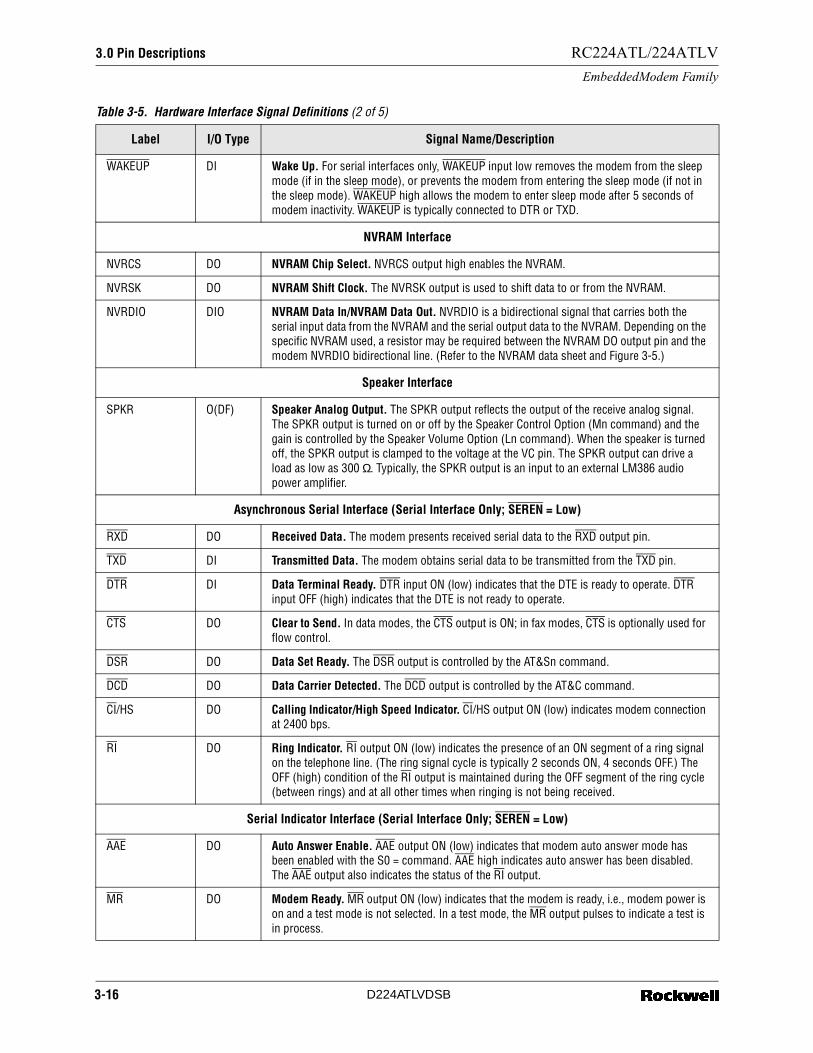
WAKEUP DI Wake Up. For serial interfaces only, WAKEUP input low removes the modem from the sleep mode (if in the sleep mode), or prevents the modem from entering the sleep mode (if not in the sleep mode). WAKEUP high allows the modem to enter sleep mode after 5 seconds of modem inactivity. WAKEUP is typically connected to DTR or TXD.
NVRAM Interface
NVRCS DO NVRAM Chip Select. NVRCS output high enables the NVRAM.
NVRSK DO NVRAM Shift Clock. The NVRSK output is used to shift data to or from the NVRAM.
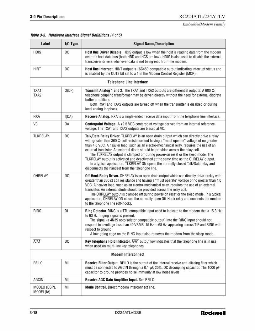
NVRDIO DIO NVRAM Data In/NVRAM Data Out. NVRDIO is a bidirectional signal that carries both the serial input data from the NVRAM and the serial output data to the NVRAM. Depending on the specific NVRAM used, a resistor may be required between the NVRAM DO output pin and the modem NVRDIO bidirectional line. (Refer to the NVRAM data sheet and Figure 3-5.)
Speaker Interface
SPKR O(DF) Speaker Analog Output. The SPKR output reflects the output of the receive analog signal. The SPKR output is turned on or off by the Speaker Control Option (Mn command) and the gain is controlled by the Speaker Volume Option (Ln command). When the speaker is turned off, the SPKR output is clamped to the voltage at the VC pin. The SPKR output can drive a load as low as 300 Ω. Typically, the SPKR output is an input to an external LM386 audio power amplifier.
Asynchronous Serial Interface (Serial Interface Only; SEREN = Low)
RXD DO Received Data. The modem presents received serial data to the RXD output pin.
TXD DI Transmitted Data. The modem obtains serial data to be transmitted from the TXD pin.
DTR DI Data Terminal Ready. DTR input ON (low) indicates that the DTE is ready to operate. DTR input OFF (high) indicates that the DTE is not ready to operate.
CTS DO Clear to Send. In data modes, the CTS output is ON; in fax modes, CTS is optionally used for flow control.
DSR DO Data Set Ready. The DSR output is controlled by the AT&Sn command.
DCD DO Data Carrier Detected. The DCD output is controlled by the AT&C command.
CI/HS DO Calling Indicator/High Speed Indicator. CI/HS output ON (low) indicates modem connection at 2400 bps.
RI DO Ring Indicator. RI output ON (low) indicates the presence of an ON segment of a ring signal on the telephone line. (The ring signal cycle is typically 2 seconds ON, 4 seconds OFF.) The OFF (high) condition of the RI output is maintained during the OFF segment of the ring cycle (between rings) and at all other times when ringing is not being received.
Serial Indicator Interface (Serial Interface Only; SEREN = Low)
AAE DO Auto Answer Enable. AAE output ON (low) indicates that modem auto answer mode has been enabled with the S0 = command. AAE high indicates auto answer has been disabled. The AAE output also indicates the status of the RI output.
MR DO Modem Ready. MR output ON (low) indicates that the modem is ready, i.e., modem power is on and a test mode is not selected. In a test mode, the MR output pulses to indicate a test is in process.
Table 3-5. Hardware Interface Signal Definitions (2 of 5)
Label I/O Type Signal Name/Description
3-16 D224ATLVDSB

3.0 Pin DescriptionsRC224ATL/224ATLV
EmbeddedModem Family
DCDL DO DCD Indicator. The DCDL output is controlled by the AT&C command.
DTRL DO DTR Indicator. The DTRL output is controlled by the AT&D command.
Parallel Host Interface (Parallel Interface Only)
When the HWT input signal is connected to the host bus write line, the parallel interface is selected upon reset. (See Order No. 821 for waveform and timing information.)
The parallel interface emulates a 16C450 UART, Table 2-1 identifies the parallel interface registers. Parallel interface operation is equivalent to 16C450 operation with CS0 and CS1 inputs high and DISTR, DOSTR, and ADS inputs low. The corresponding RC224ATL/V and 16C450 signals are shown below. 16C450 signals not required for RC224ATL/V host computer operation are not shown.16C450 Signal RC224ATL/V Signal
A0 - A2 HA0 - HA2D0 - D7 HD0 - HD7MR RESET (Active low)CS2 HCSDISTR HWTDOSTR HRDINTRPT HINTDDIS HDISOUT2 None (Implemented internally in RC224ATL/V)
HA0-HA2
HD0-HD7
DI
DIO
Host Bus Address Lines 0-2. During a host read or write operation, HA0-HA2 select an internal register. The state of the divisor latch access bit (DLAB) affects the selection of certain registers. The register addresses are:
Host Bus Data Lines 0-7. HD0-HD7 are comprised of eight tri-state input/output lines providing bidirectional communication between the host and the modem. Data, control words, and status information are transferred through HD0-HD7.
HCS DI Host Bus Chip Select. HCS input low enables reading from or writing to the modem using the parallel bus.
HRD DI Host Bus Read. HRD is an active low read control input. When the modem is selected with HCS, HRD low allows status or data words to be read from an addressed register.
HWT DI Host Bus Write. HWT is an active low write control input. When the modem is selected with HCS, HWT low allows data or control words to be written to an addressed register.
Table 3-5. Hardware Interface Signal Definitions (3 of 5)
Label I/O Type Signal Name/Description
DLAB HA2 HA1 HA0 Register0 0 0 0 Receive Buffer Register (Read),
Transmitter Holding Register (Write)0 0 0 1 Interrupt Enable RegisterX 0 1 0 Interrupt Identification Register (Read Only)X 0 1 1 Line Control RegisterX 1 0 0 Modem Control RegisterX 1 0 1 Line Status Register (Read Only)X 1 1 1 Scratch Register1 0 0 0 Divisor Latch Register (Least Significant Byte)1 0 0 1 Divisor Latch Register (Most Significant Byte)
3-17 D224ATLVDSB
3.0 Pin Descriptions
RC224ATL/224ATLV
EmbeddedModem Family
HDIS DO Host Bus Driver Disable. HDIS output is low when the host is reading data from the modem over the host data bus (both HRD and HCS are low). HDIS is also used to disable the external transceiver drivers whenever data is not being read from the modem.
HINT DO Host Bus Interrupt. HINT output is 16C450-compatible output indicating interrupt status and is enabled by the OUT2 bit set to a 1 in the Modem Control Register (MCR).
Telephone Line Interface
TXA1TXA2
O(DF) Transmit Analog 1 and 2. The TXA1 and TXA2 outputs are differential outputs. A 600 Ω telephone coupling transformer may be driven directly without the need for external discrete buffer amplifiers.
Both TXA1 and TXA2 outputs are turned off when the transmitter is disabled or during local analog loopback.
RXA I(DA) Receive Analog. RXA is a single-ended receive data input from the telephone line interface.
VC OA Centerpoint Voltage. A +2.5 VDC centerpoint voltage derived from an internal reference voltage. The TXA1 and TXA2 outputs are biased at VC.
TLKRELAY DO Talk/Data Relay Driver. TLKRELAY is an open drain output which can directly drive a relay with greater than 360 Ω coil resistance and having a “must operate” voltage of no greater than 4.0 VDC. A heavier load, such as an electro-mechanical relay, requires the use of an external transistor. An external diode should be provided across the relay coil.
The TLKRELAY output is clamped off during power-on reset or the sleep mode. The TLKRELAY output is activated and deactivated at the same time as the OHRELAY output.
In a typical application, TLKRELAY ON opens the normally closed Talk/Data relay and disconnects the handset from the telephone line.
OHRELAY DO Off-Hook Relay Driver. OHRELAY is an open drain output which can directly drive a relay with greater than 360 Ω coil resistance and having a “must operate” voltage of no greater than 4.0 VDC. A heavier load, such as an electro-mechanical relay, requires the use of an external transistor. An external diode should be provided across the relay coil.
The OHRELAY output is clamped off during power-on reset or the sleep mode. In a typical application, OHRELAY ON closes the normally open Off-Hook relay and connects the modem to the telephone line (off-hook).
RING DI Ring Detector. RING is a TTL-compatible input used to indicate to the modem that a 15.3 Hz to 63 Hz ringing signal is present.
The signal (a 4N35 optoisolator compatible output) into the RING input should not respond to a voltage less than 40 VRMS, 15 Hz to 68 Hz, appearing across TIP and RING with respect to ground.
A low-going edge on the RING input also removes the modem from the sleep mode.
A/A1 DO Key Telephone Hold Indicator. A/A1 output low indicates that the telephone line is in use when used on multi-line key telephones.
Modem Interconnect
RFILO MI Receive Filter Output. RFILO is the output of the internal receive anti-aliasing filter which must be connected to AGCIN through a 0.1 µF, 20%, DC decoupling capacitor. The 1000 pF capacitor to ground provides noise immunity at low noise levels.
AGCIN MI Receive AGC Gain Amplifier Input. See RFILO.
MODEO (DSP), MODEI (IA)
MI Mode Control. Direct modem interconnect line.
Table 3-5. Hardware Interface Signal Definitions (4 of 5)
Label I/O Type Signal Name/Description
3-18 D224ATLVDSB
3.0 Pin DescriptionsRC224ATL/224ATLV
EmbeddedModem Family
TDACO (DSP), TDACI (IA)
MI Transmitter DAC Signal. Serial digital DAC signal. Direct modem interconnect line.
TSTBO (DSP), TSTBI (IA)
MI Transmitter Strobe. 576 kHz digital transmitter timing reference. Direct modem interconnect line.
TRSTO (DSP), TRSTI (IA)
MI Transmitter Reset. 9.6 kHz, 8228.57 Hz, or 7.2 kHz digital transmitter timing reference. Direct modem interconnect line. Direct modem interconnect line.
RADCI (DSP), RADCO (IA)
MI Receiver ADC Signal. Serial digital ADC signal. Direct modem interconnect line.
RAGCO (DSP), RAGCI (IA)
MI Receiver AGC Signal. Serial digital AGC signal. Direct modem interconnect line.
RRSTO (DPS), RRSTI (IA)
MI Receiver Reset. 9.6 kHz, 8228.57 Hz, or 7.2 kHz digital receiver timing reference. Direct modem interconnect line.
RSTBO (DSP), RSTBI (IA)
MI Receiver Strobe. 576 kHz digital receiver timing reference. Direct modem interconnect line.
Table 3-5. Hardware Interface Signal Definitions (5 of 5)
Label I/O Type Signal Name/Description
3-19 D224ATLVDSB
3.0 Pin Descriptions
RC224ATL/224ATLV
EmbeddedModem Family
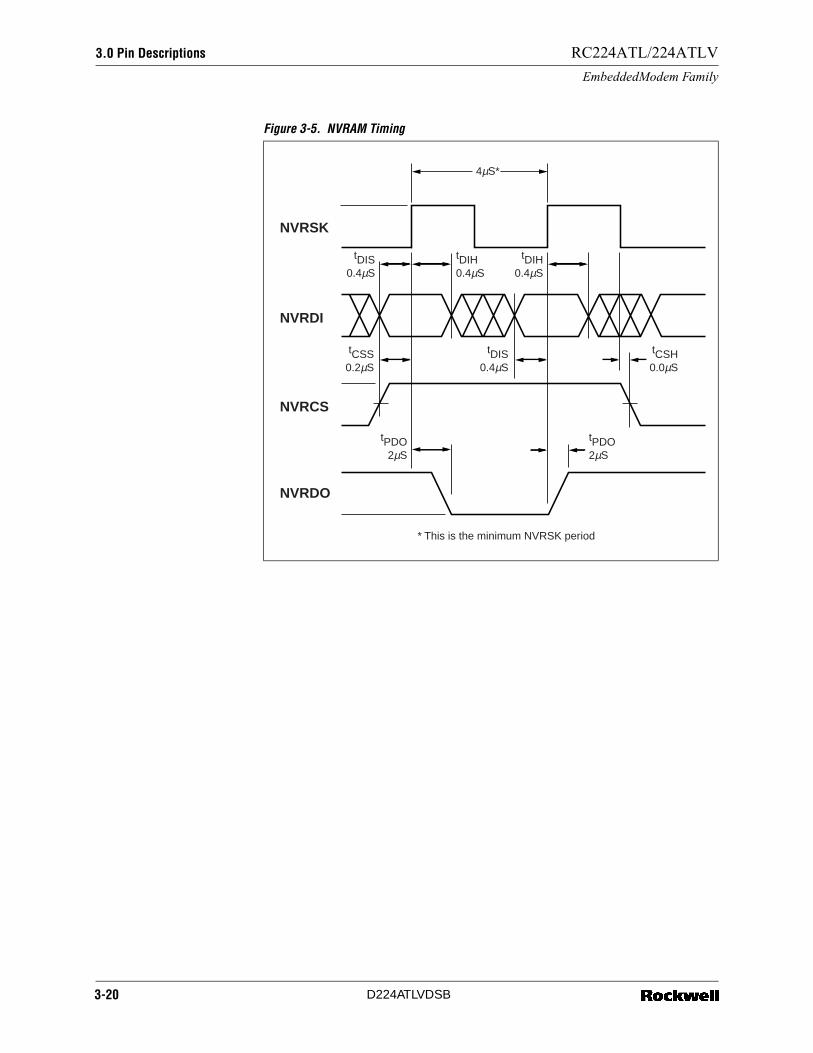
Figure 3-5. NVRAM Timing
4µS*
NVRSK
NVRDI
NVRCS
NVRDO
tDIS0.4µS
tDIS0.4µS
tPDO2µS
tPDO2µS
tCSS0.2µS
tCSH0.0µS
tDIH0.4µS
tDIH0.4µS
* This is the minimum NVRSK period
3-20 D224ATLVDSB

4.0 AT Commands
4.1 AT Command Format
Each command line must start with the AT prefix and be terminated with a carriage return (CR). Several commands may be included on one command line. A command line may contain up to 40 characters excluding the AT prefix and the terminating CR. A separator is not required between data commands. A semicolon (;) separator is required between fax commands.
AT commands are composed of 10-bit ASCII encoded asynchronous characters. The character format in data mode is 8 data bits with no parity, or 7 data bits with even, odd, or no (two stop bits) parity, at a data rate of 19200, 2400, 1200, or 300 bps. The character format in fax mode is 8 data bits with no parity at 19200 bps.
Table 4-1. Result Codes and Messages (1 of 2)
Digital Code Word Code Meaning
0 OK Command line executed without errors
1 CONNECT Connection at 300 bps
2 RING Ringing signal detected
3 NO CARRIER Carrier lost or never present
4 ERROR Invalid command, checksum, error in command line, or command line exceeds 40 characters
5 CONNECT 1200 Connection at 1200 bps
6 NO DIALTONE No dialtone detected
7 BUSY Busy signal detected
8 NO ANSWER No silence detected when dialing a system not providing a dialtone
4-1 D224ATLVDSB
4.0 AT Commands 4.1 AT Command Format
RC224ATL/224ATLV
EmbeddedModem Family
10 CONNECT 2400 Connection at 2400 bps
+F4 +FCERROR Fax carrier error
13 DATA Connected as data modem during auto answer
15 FAX Connected as fax modem during auto answer
Table 4-1. Result Codes and Messages (2 of 2)
Digital Code Word Code Meaning
Table 4-2. “AT” Command Set Summary (1 of 6)
Command Function Default Parameters/Description
A/ Re-execute command
A Answer a call
AT Command line prefixParameters: none
Attention Code. Precedes the command line except for +++ (escape) and A/ (repeat) commands.
Bn Select CCITT or Bell Mode
Parameters: n=0,1
n=1 n=0 Selects CCITT operation at 300 or 1200 bps during Call Establishment and a subsequent connection.
n=1 Selects BELL operation at 300 or 1200 bps during Call Establishment and a subsequent connection.
Cn Carrier controlParameters: n=0,1
n=1
D Dial Command. D causes the modem to dial the number which follows the D in the command line. Valid dial characteristics are 0 to 9, A to D, #, and *. Other valid dial modifier characters are: “,” P, R, S=n, T, W, “;”, @, and !.
Dn Dial modifier
En Command echoParameters: n=0,1
n=1 n=0 Disables command echo.
n=1 Enables command echo.
Fn On-line character echo optionParameters: n=0,1
n=1 n=0 Returns ERROR result code.
n=1 Returns OK result code.
Hn Disconnect (hang-up)Parameters: n=0,1
n=0 n=0 Modem on-hook (relay open).
n=1 Modem off-hook (relay closed).
4-2 D224ATLVDSB

4.0 AT Commands
4.1 AT Command Format
RC224ATL/224ATLV
EmbeddedModem Family
In Identification
Parameters: n=0,1,2,3
n=0 n=0 Reports product identification code.
n=1 Calculates the ROM checksum.
n=2 Calculates the ROM checksum and compares it with the prestored checksum. Reports "OK" if the calculated checksum equals the prestored checksum or if the prestored checksum value is FFh; otherwise reports “ERROR”.
n=3 Reports the firmware version and ROM part number.
Ln Speaker volumeParameters: n=0,1,2,3
n=2 n=0 Low volume.n=1 Low volume. n=2 Medium volume.n=3 High volume.
Mn Speaker controlParameters: n=0,1,2,3
n=1 n=0 Speaker is always off.n=1 Speaker is on during Call Establishment, but off when
receiving carrier. n=2 Speaker is always on.n=3 Speaker is on after dialing, until carrier is detected.
On Go on-lineParameters: n=0,1
n=0 On-line state.n=1 On-line state with equalizer retrain.
P Force pulse dialing
Qn Quiet Result codes control n=0 n=0 Enables result codes to the DTE. n=1 Disables result codes to the DTE.
Sn Select S register as defaultRange: n=0-27
n Establishes S-Register n as the last register accessed.n=v Sets S-Register n to the value v.n? Reports the value of S-Register n.
Sn= Parameters: noneRange:n=0-27 (register no.)
x=0-255 (value)
Write to an S Register. Sr=x sets register “n” to the value “x”. Configuration registers are provided to retain modem configuration parameters. The contents of these registers can be modified with this command.
Sn? Parameters: noneRange: n=0-27
Read an S register. Sn? causes the contents stored in register “n” to be returned.
T Force DTMF dialing
Vn Report codes form n=1 n=0 Result code is sent as a digit.n=1 Result code is send a ASCII text.
Table 4-2. “AT” Command Set Summary (2 of 6)
Command Function Default Parameters/Description
4-3 D224ATLVDSB
4.0 AT Commands 4.1 AT Command Format
RC224ATL/224ATLV
EmbeddedModem Family
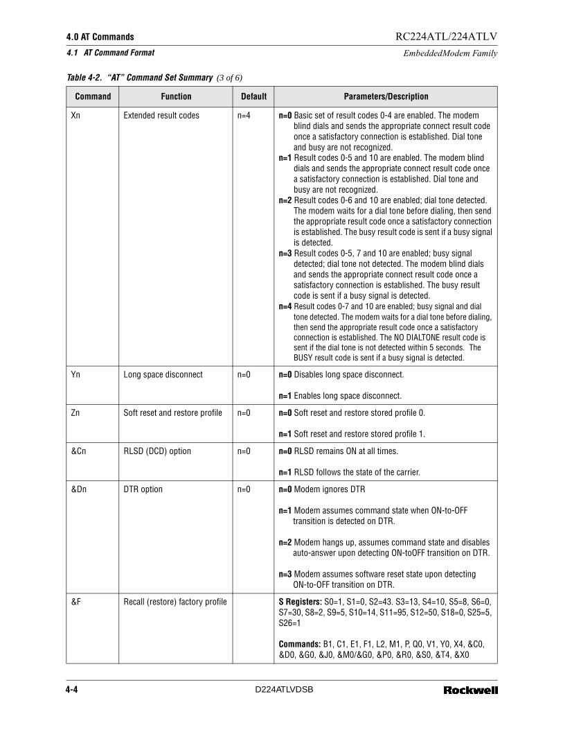
Xn Extended result codes n=4 n=0 Basic set of result codes 0-4 are enabled. The modem blind dials and sends the appropriate connect result code once a satisfactory connection is established. Dial tone and busy are not recognized.
n=1 Result codes 0-5 and 10 are enabled. The modem blind dials and sends the appropriate connect result code once a satisfactory connection is established. Dial tone and busy are not recognized.
n=2 Result codes 0-6 and 10 are enabled; dial tone detected. The modem waits for a dial tone before dialing, then send the appropriate result code once a satisfactory connection is established. The busy result code is sent if a busy signal is detected.
n=3 Result codes 0-5, 7 and 10 are enabled; busy signal detected; dial tone not detected. The modem blind dials and sends the appropriate connect result code once a satisfactory connection is established. The busy result code is sent if a busy signal is detected.
n=4 Result codes 0-7 and 10 are enabled; busy signal and dial tone detected. The modem waits for a dial tone before dialing, then send the appropriate result code once a satisfactory connection is established. The NO DIALTONE result code is sent if the dial tone is not detected within 5 seconds. The BUSY result code is sent if a busy signal is detected.
Yn Long space disconnect n=0 n=0 Disables long space disconnect.
n=1 Enables long space disconnect.
Zn Soft reset and restore profile n=0 n=0 Soft reset and restore stored profile 0.
n=1 Soft reset and restore stored profile 1.
&Cn RLSD (DCD) option n=0 n=0 RLSD remains ON at all times.
n=1 RLSD follows the state of the carrier.
&Dn DTR option n=0 n=0 Modem ignores DTR
n=1 Modem assumes command state when ON-to-OFF transition is detected on DTR.
n=2 Modem hangs up, assumes command state and disables auto-answer upon detecting ON-toOFF transition on DTR.
n=3 Modem assumes software reset state upon detecting ON-to-OFF transition on DTR.
&F Recall (restore) factory profile S Registers: S0=1, S1=0, S2=43. S3=13, S4=10, S5=8, S6=0, S7=30, S8=2, S9=5, S10=14, S11=95, S12=50, S18=0, S25=5, S26=1
Commands: B1, C1, E1, F1, L2, M1, P, Q0, V1, Y0, X4, &C0, &D0, &G0, &J0, &M0/&G0, &P0, &R0, &S0, &T4, &X0
Table 4-2. “AT” Command Set Summary (3 of 6)
Command Function Default Parameters/Description
4-4 D224ATLVDSB
4.0 AT Commands
4.1 AT Command Format
RC224ATL/224ATLV
EmbeddedModem Family
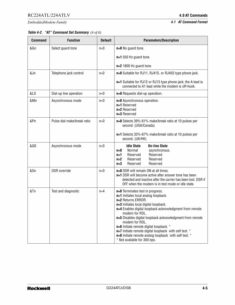
&Gn Select guard tone n=0 n=0 No guard tone.
n=1 550 Hz guard tone.
n=2 1800 Hz guard tone.
&Jn Telephone jack control n=0 n=0 Suitable for RJ11, RJ41S. or RJ45S type phone jack.
n=1 Suitable for RJ12 or RJ13 type phone jack; the A lead ia connected to A1 lead while the modem is off-hook.
&L0 Dial-up line operation n=0 n=0 Requests dial-up operation.
&Mn Asynchronous mode n=0 n=0 Asynchronous operation.n=1 Reservedn=2 Reservedn=3 Reserved
&Pn Pulse dial make/break ratio n=0 n=0 Selects 39%-61% make/break ratio at 10 pulses per second. (USA/Canada)
n=1 Selects 33%-67% make/break ratio at 10 pulses per second. (UK/HK)
&Q0 Asynchronous mode n=0 Idle State On-line Staten=0 Normal asynchronous. n=1 Reserved Reservedn=2 Reserved Reservedn=3 Reserved Reserved
&Sn DSR override n=0 n=0 DSR will remain ON at all times. n=1 DSR will become active after answer tone has been
detected and inactive after the carrier has been lost. DSR if OFF when the modem is in test mode or idle state.
&Tn Test and diagnostic n=4 n=0 Terminates test in progress. n=1 Initiates local analog loopback.n=2 Returns ERROR.n=3 Initiates local digital loopback.n=4 Enables digital loopback acknowledgment from remote
modem for RDL.n=5 Disables digital loopback acknowledgment from remote
modem for RDL.n=6 Initiate remote digital loopback. *n=7 Initiate remote digital loopback with self test. *n=8 Initiate remote analog loopback with self test. ** Not available for 300 bps.
Table 4-2. “AT” Command Set Summary (4 of 6)
Command Function Default Parameters/Description
4-5 D224ATLVDSB
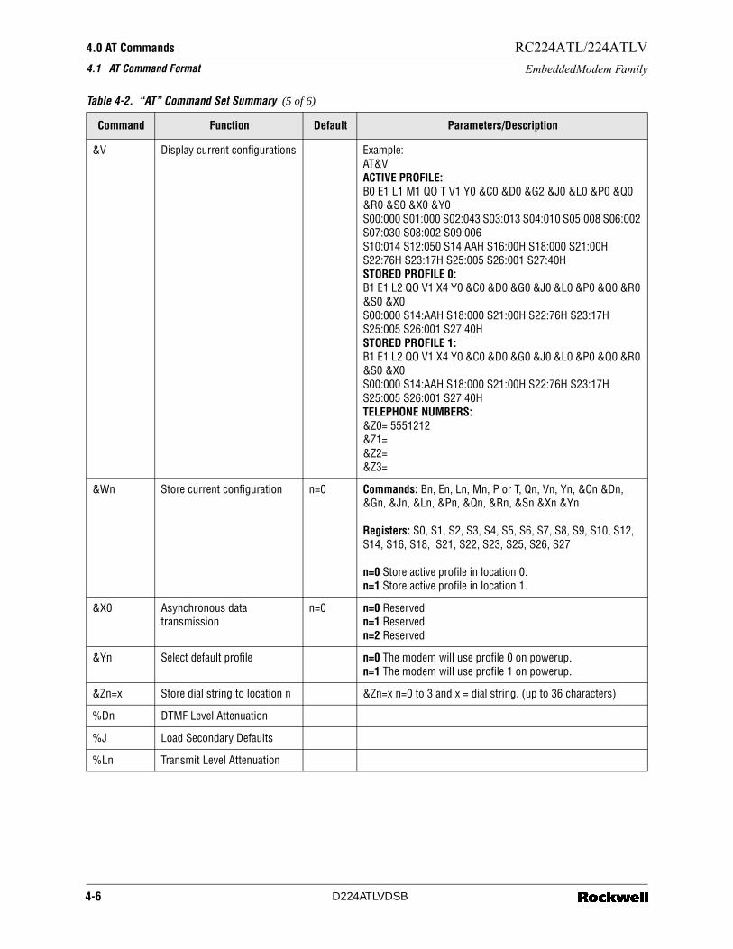
4.0 AT Commands 4.1 AT Command Format
RC224ATL/224ATLV
EmbeddedModem Family
&V Display current configurations Example:AT&VACTIVE PROFILE:B0 E1 L1 M1 QO T V1 Y0 &C0 &D0 &G2 &J0 &L0 &P0 &Q0 &R0 &S0 &X0 &Y0S00:000 S01:000 S02:043 S03:013 S04:010 S05:008 S06:002 S07:030 S08:002 S09:006S10:014 S12:050 S14:AAH S16:00H S18:000 S21:00H S22:76H S23:17H S25:005 S26:001 S27:40HSTORED PROFILE 0:B1 E1 L2 QO V1 X4 Y0 &C0 &D0 &G0 &J0 &L0 &P0 &Q0 &R0 &S0 &X0 S00:000 S14:AAH S18:000 S21:00H S22:76H S23:17H S25:005 S26:001 S27:40H STORED PROFILE 1:B1 E1 L2 QO V1 X4 Y0 &C0 &D0 &G0 &J0 &L0 &P0 &Q0 &R0 &S0 &X0 S00:000 S14:AAH S18:000 S21:00H S22:76H S23:17H S25:005 S26:001 S27:40H TELEPHONE NUMBERS:&Z0= 5551212&Z1=&Z2=&Z3=
&Wn Store current configuration n=0 Commands: Bn, En, Ln, Mn, P or T, Qn, Vn, Yn, &Cn &Dn, &Gn, &Jn, &Ln, &Pn, &Qn, &Rn, &Sn &Xn &Yn
Registers: S0, S1, S2, S3, S4, S5, S6, S7, S8, S9, S10, S12, S14, S16, S18, S21, S22, S23, S25, S26, S27
n=0 Store active profile in location 0.n=1 Store active profile in location 1.
&X0 Asynchronous data transmission
n=0 n=0 Reservedn=1 Reservedn=2 Reserved
&Yn Select default profile n=0 The modem will use profile 0 on powerup.n=1 The modem will use profile 1 on powerup.
&Zn=x Store dial string to location n &Zn=x n=0 to 3 and x = dial string. (up to 36 characters)
%Dn DTMF Level Attenuation
%J Load Secondary Defaults
%Ln Transmit Level Attenuation
Table 4-2. “AT” Command Set Summary (5 of 6)
Command Function Default Parameters/Description
4-6 D224ATLVDSB

4.0 AT Commands
4.1 AT Command Format
RC224ATL/224ATLV
EmbeddedModem Family
Dial Modifier
Function
P Pulse Dial
Parameters: none
R Originate Call in Answer Mode
Parameters: none
S=n Dial Stored Number
Parameters:n=0, 1, 2, 3
S<CR>S=<CR>S=n<CR> where n=0-3
T Tone Dial
Parameters: none
W Wait for Dial ToneParameters: none
; Return to Idle StateParameters: none
@ Wait for Quiet Answer CommandParameters: none
! Flash HookParameters: none
, (comma) PauseParameters: none
0-9, A, B, C, D, #, *
Dial Digits/CharactersParameters: none
Table 4-2. “AT” Command Set Summary (6 of 6)
Command Function Default Parameters/Description
4-7 D224ATLVDSB
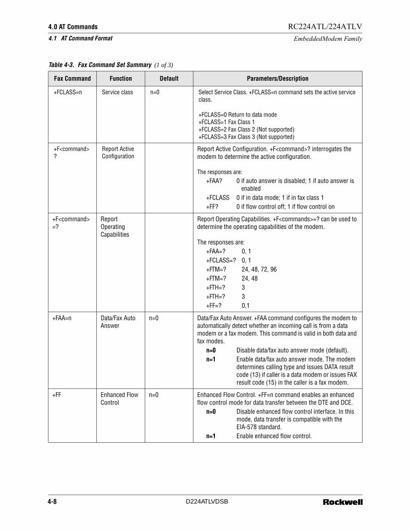
4.0 AT Commands 4.1 AT Command Format
RC224ATL/224ATLV
EmbeddedModem Family
Table 4-3. Fax Command Set Summary (1 of 3)
Fax Command Function Default Parameters/Description
+FCLASS=n Service class n=0 Select Service Class. +FCLASS=n command sets the active service class.
+FCLASS=0 Return to data mode+FCLASS=1 Fax Class 1+FCLASS=2 Fax Class 2 (Not supported)+FCLASS=3 Fax Class 3 (Not supported)
+F<command>?
Report Active Configuration
Report Active Configuration. +F<command>? interrogates the modem to determine the active configuration.
The responses are:+FAA? 0 if auto answer is disabled; 1 if auto answer is
enabled+FCLASS 0 if in data mode; 1 if in fax class 1+FF? 0 if flow control off; 1 if flow control on
+F<command>=?
Report Operating Capabilities
Report Operating Capabilities. +F<commands>=? can be used to determine the operating capabilities of the modem.
The responses are:+FAA=? 0, 1+FCLASS=? 0, 1+FTM=? 24, 48, 72, 96+FTM=? 24, 48+FTH=? 3+FTH=? 3+FF=? 0,1
+FAA=n Data/Fax Auto Answer
n=0 Data/Fax Auto Answer. +FAA command configures the modem to automatically detect whether an incoming call is from a data modem or a fax modem. This command is valid in both data and fax modes.
n=0 Disable data/fax auto answer mode (default).n=1 Enable data/fax auto answer mode. The modem
determines calling type and issues DATA result code (13) if caller is a data modem or issues FAX result code (15) in the caller is a fax modem.
+FF Enhanced Flow Control
n=0 Enhanced Flow Control. +FF=n command enables an enhanced flow control mode for data transfer between the DTE and DCE.
n=0 Disable enhanced flow control interface. In this mode, data transfer is compatible with the EIA-578 standard.
n=1 Enable enhanced flow control.
4-8 D224ATLVDSB

4.0 AT Commands
4.1 AT Command Format
RC224ATL/224ATLV
EmbeddedModem Family
+FTS=n Stop Transmission and Wait
n=0 Stop Transmission and Wait. +FTS=n causes the modem to terminate a transmission. After temination the modem waits for n 10 millisecond intervals before responding with the OK result code. An ERROR response code results if this command is issued while the modem is on-hook.
+FRS=n Receive Silence n=0 Receive Silence. +FRS=n causes the modem to report back to the DTE with an OK result code after n 10 millisecond intervals of silence have been detected on the line. This command is aborted if any command character is received. The modem discards the aborting character and issues an OK result code. An ERROR response code results if this command is issued while the modem is on-hook.
+FTM=n Transmit Data n=48 Transmit Data. +FTM=n causes the modem to transmit data using the modulation defined below. An ERROR response code results if this command is issued while the modem is on-hook.
+FTM=24 V.27 ter 2400 bps+FTM=48 V.27 ter 4800 bps+FTM=72 V.29 7200 bps+FTM=96 V.29 9600 bps
+FRM=n Receive Data n=48 Receive Data. +FRM=n causes the modem to enter the receiver mode using the modulation defined below. An ERROR response code results if this command is issued while the modem is on-hook.
+FRM=24 V.27 ter 2400 bps+FRM=48 V.27 ter 4800 bps+FRM=72 V.29 7200 bps (Not supported*)+FRM=96 V.29 9600 bps (Not supported*)* Modem will respond with ERROR result code.
+FTH=n Transmit Data with HDLC Framing
n=3 Transmit Data with HDLC Framing. +FTH=n causes the modem to transmit data framed in HDLC protocol using the modulation defined below. An ERROR response code results if this command is issued while the modem is on-hook.
+FTH=3 V.21 Channel 2300 bps
Table 4-3. Fax Command Set Summary (2 of 3)
Fax Command Function Default Parameters/Description
4-9 D224ATLVDSB
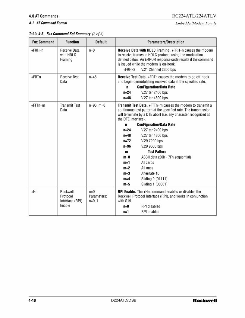
4.0 AT Commands 4.1 AT Command Format
RC224ATL/224ATLV
EmbeddedModem Family
+FRH=n Receive Data with HDLC Framing
n=0 Receive Data with HDLC Framing. +FRH=n causes the modem to receive frames in HDLC protocol using the modulation defined below. An ERROR response code results if the command is issued while the modem is on-hook.
+FRH=3 V.21 Channel 2300 bps
+FRTn Receive Test Data
n=48 Receive Test Data. +FRTn causes the modem to go off-hook and begin demodulating received data at the specified rate.
n ConFiguration/Data Raten=24 V.27 ter 2400 bpsn=48 V.27 ter 4800 bps
+FTTn=m Transmit Test Data
n=96, m=0 Transmit Test Data. +FTTn=m causes the modem to transmit a continuous test pattern at the specified rate. The transmission will terminate by a DTE abort (i.e. any character recognized at the DTE interface).
n ConFiguration/Data Raten=24 V.27 ter 2400 bpsn=48 V.27 ter 4800 bpsn=72 V.29 7200 bpsn=96 V.29 9600 bpsm Test Pattern
m=0 ASCII data (20h - 7Fh sequential)m=1 All zerosm=2 All onesm=3 Alternate 10m=4 Sliding 0 (01111)m=5 Sliding 1 (00001)
+Hn Rockwell Protocol Interface (RPI) Enable
n=0Parameters:n=0, 1
RPI Enable. The +Hn command enables or disables the Rockwell Protocol Interface (RPI), and works in conjunction with S19.
n=0 RPI disabledn=1 RPI enabled
Table 4-3. Fax Command Set Summary (3 of 3)
Fax Command Function Default Parameters/Description
4-10 D224ATLVDSB
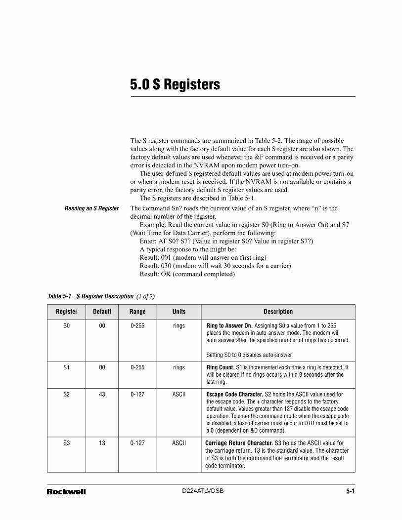
5.0 S Registers
The S register commands are summarized in Table 5-2. The range of possible values along with the factory default value for each S register are also shown. The factory default values are used whenever the &F command is received or a parity error is detected in the NVRAM upon modem power turn-on.
The user-defined S registered default values are used at modem power turn-on or when a modem reset is received. If the NVRAM is not available or contains a parity error, the factory default S register values are used.
The S registers are described in Table 5-1.
Reading an S Register The command Sn? reads the current value of an S register, where “n” is the decimal number of the register.
Example: Read the current value in register S0 (Ring to Answer On) and S7 (Wait Time for Data Carrier), perform the following:
Enter: AT S0? S7? (Value in register S0? Value in register S7?)A typical response to the might be:Result: 001 (modem will answer on first ring)Result: 030 (modem will wait 30 seconds for a carrier)Result: OK (command completed)
Table 5-1. S Register Description (1 of 3)
Register Default Range Units Description
S0 00 0-255 rings Ring to Answer On. Assigning S0 a value from 1 to 255 places the modem in auto-answer mode. The modem will auto answer after the specified number of rings has occurred.
Setting S0 to 0 disables auto-answer.
S1 00 0-255 rings Ring Count. S1 is incremented each time a ring is detected. It will be cleared if no rings occurs within 8 seconds after the last ring.
S2 43 0-127 ASCII Escape Code Character. S2 holds the ASCII value used for the escape code. The + character responds to the factory default value. Values greater than 127 disable the escape code operation. To enter the command mode when the escape code is disabled, a loss of carrier must occur to DTR must be set to a 0 (dependent on &D command).
S3 13 0-127 ASCII Carriage Return Character. S3 holds the ASCII value for the carriage return. 13 is the standard value. The character in S3 is both the command line terminator and the result code terminator.
5-1 D224ATLVDSB
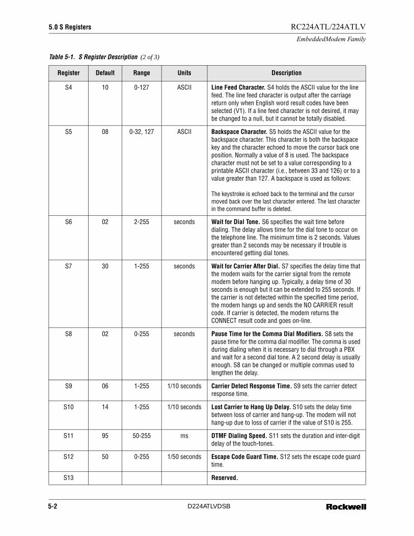
5.0 S Registers
RC224ATL/224ATLV
EmbeddedModem Family
S4 10 0-127 ASCII Line Feed Character. S4 holds the ASCII value for the line feed. The line feed character is output after the carriage return only when English word result codes have been selected (V1). If a line feed character is not desired, it may be changed to a null, but it cannot be totally disabled.
S5 08 0-32, 127 ASCII Backspace Character. S5 holds the ASCII value for the backspace character. This character is both the backspace key and the character echoed to move the cursor back one position. Normally a value of 8 is used. The backspace character must not be set to a value corresponding to a printable ASCII character (i.e., between 33 and 126) or to a value greater than 127. A backspace is used as follows:
The keystroke is echoed back to the terminal and the cursor moved back over the last character entered. The last character in the command buffer is deleted.
S6 02 2-255 seconds Wait for Dial Tone. S6 specifies the wait time before dialing. The delay allows time for the dial tone to occur on the telephone line. The minimum time is 2 seconds. Values greater than 2 seconds may be necessary if trouble is encountered getting dial tones.
S7 30 1-255 seconds Wait for Carrier After Dial. S7 specifies the delay time that the modem waits for the carrier signal from the remote modem before hanging up. Typically, a delay time of 30 seconds is enough but it can be extended to 255 seconds. If the carrier is not detected within the specified time period, the modem hangs up and sends the NO CARRIER result code. If carrier is detected, the modem returns the CONNECT result code and goes on-line.
S8 02 0-255 seconds Pause Time for the Comma Dial Modifiers. S8 sets the pause time for the comma dial modifier. The comma is used during dialing when it is necessary to dial through a PBX and wait for a second dial tone. A 2 second delay is usually enough. S8 can be changed or multiple commas used to lengthen the delay.
S9 06 1-255 1/10 seconds Carrier Detect Response Time. S9 sets the carrier detect response time.
S10 14 1-255 1/10 seconds Lost Carrier to Hang Up Delay. S10 sets the delay time between loss of carrier and hang-up. The modem will not hang-up due to loss of carrier if the value of S10 is 255.
S11 95 50-255 ms DTMF Dialing Speed. S11 sets the duration and inter-digit delay of the touch-tones.
S12 50 0-255 1/50 seconds Escape Code Guard Time. S12 sets the escape code guard time.
S13 Reserved.
Table 5-1. S Register Description (2 of 3)
Register Default Range Units Description
5-2 D224ATLVDSB
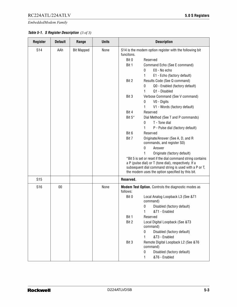
5.0 S RegistersRC224ATL/224ATLV
EmbeddedModem Family
S14 AAh Bit Mapped None S14 is the modem option register with the following bit funcitons.
Bit 0 ReservedBit 1 Command Echo (See E command)
0 E0 - No echo1 E1 - Echo (factory default)
Bit 2 Results Code (See Q command)0 Q0 - Enabled (factory default)1 Q1 - Disabled
Bit 3 Verbose Command (See V command)0 V0 - Digits1 V1 - Words (factory default)
Bit 4 ReservedBit 5* Dial Method (See T and P commands)
0 T - Tone dial1 P - Pulse dial (factory default)
Bit 6 ReservedBit 7 Originate/Answer (See A, D, and R
commands, and register S0)0 Answer1 Originate (factory default)
*Bit 5 is set or reset if the dial command string contains a P (pulse dial) or T (tone dial), respectively. If a subsequent dial command string is used with a P or T, the modem uses the option specified by this bit.
S15 Reserved.
S16 00 None Modem Test Option. Controls the diagnostic modes as follows:
Bit 0 Local Analog Loopback L3 (See &T1 command)0 Disabled (factory default)1 &T1 - Enabled
Bit 1 ReservedBit 2 Local Digital Loopback (See &T3
command)0 Disabled (factory default)1 &T3 - Enabled
Bit 3 Remote Digital Loopback L2 (See &T6 command)0 Disabled (factory default)1 &T6 - Enabled
Table 5-1. S Register Description (3 of 3)
Register Default Range Units Description
5-3 D224ATLVDSB

5.0 S Registers
RC224ATL/224ATLV
EmbeddedModem Family
Table 5-2. S Register Summary
Register Range Units Default Description
S0* 0-255 rings 00 Rings to Auto-Answer
S1 0-255 rings 00 Ring Counter
S2 0-127 ASCII 43 Escape Character
S3 0-127 ASCII 13 Carriage Return Character
S4 0-127 ASCII 10 Line Feed Character
S5 0-32, 127 ASCII 08 Backspace Character
S6 2-255 seconds 02 Maximum time to Wait for Dial Tone
S7 1-255 seconds 30 Wait for Carrier
S8 0-255 seconds 02 Pause Time for Comma
S9 1-255 1/10 seconds 06 Carrier Detect Response Time
S10 1-255 1/10 seconds 14 Carrier Loss Disconnect Time
S11 50-255 ms 95 DTMF Dialing Speed
S12 0-255 1/50 seconds 50 Escape Prompt Delay
S14* Bit Mapped none AA hex General Bit Mapped Options
S16 Bit Mapped none 00 Test Mode Bit Mapped Options (&T)
S17 0-250 4 ms increments 00 Fax Mode Null Byte Timer
S18* 0-255 seconds 00 Test Timer
S19 0-1 none 00 Rockwell Protocol Interface Speed
S20 0-127 seconds 00 Fax Mode Inactivity Timer
S21* Bit Mapped none 00 General Bit Mapped Options
S22* Bit Mapped none 76 hex General Bit Mapped Options
S23* Bit Mapped none 07 General Bit Mapped Options
S24 0-255 seconds 00 Sleep Inactivity Timer
S25* 0-255 0.1 or 1 seconds 05 Delay to DTR Off
S26* 0-255 0.01 seconds 1 RTS-to-CTS Delay
S27* Bit Mapped none 40 hex General Bit Mapped Options
S28* Bit Mapped none 00 General Bit-Mapped Options
* Register value may be stored in one of two user profiles with the AT&W command.
5-4 D224ATLVDSB
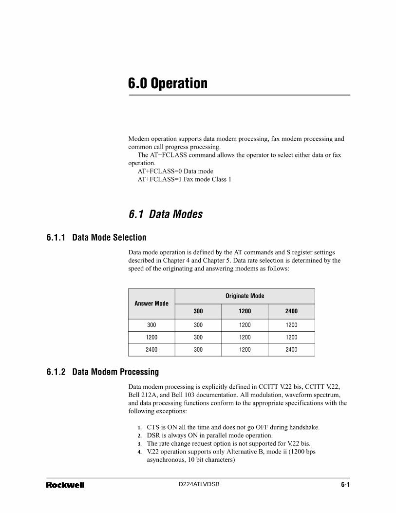
6.0 Operation
Modem operation supports data modem processing, fax modem processing and common call progress processing.
The AT+FCLASS command allows the operator to select either data or fax operation.
AT+FCLASS=0 Data modeAT+FCLASS=1 Fax mode Class 1
6.1 Data Modes
6.1.1 Data Mode Selection
Data mode operation is defined by the AT commands and S register settings described in Chapter 4 and Chapter 5. Data rate selection is determined by the speed of the originating and answering modems as follows:
6.1.2 Data Modem Processing
Data modem processing is explicitly defined in CCITT V.22 bis, CCITT V.22, Bell 212A, and Bell 103 documentation. All modulation, waveform spectrum, and data processing functions conform to the appropriate specifications with the following exceptions:
1. CTS is ON all the time and does not go OFF during handshake.2. DSR is always ON in parallel mode operation.3. The rate change request option is not supported for V.22 bis.4. V.22 operation supports only Alternative B, mode ii (1200 bps
asynchronous, 10 bit characters)
Answer ModeOriginate Mode
300 1200 2400
300 300 1200 1200
1200 300 1200 1200
2400 300 1200 2400
6-1 D224ATLVDSB

6.0 Operation 6.2 Fax Modes
RC224ATL/224ATLV
EmbeddedModem Family
6.1.3 Call Origination
Automatic and manual origination of calls is supported. Automatic call origination is supported by the ATDS command. The modem automatically enters the data handshaking mode upon completion of the dial function.
6.1.4 Call Answering
Automatic and manual answering of calls is supported. Incoming ring signals are detected by the modem and indicated by the RING result code. Answering can be performed by the DTE acknowledging the RING result code and issuing the ATA command or by having the modem automatically go off-hook after N rings are detected. The number of rings, N, is determined by the setting of the S0 register. Upon going off-hook, the DCE will transmit 2100 Hz (or 2225 Hz for Bell modes) for a duration of not less than 2.6 seconds and not more than 4.0 seconds.
6.1.5 Call Termination
A call is terminated by the DTE sending the ATH command to the modem.
6.1.5.1 Rockwell Proto-col Interface (RPI)
The RPI is a RC224ATLV feature, which when enabled by the AT+H1 command prior to establishing a modem to modem data connection, allows Data Applications Protocol Interface (DAPI) host software to provide full error correction (V.42 LAPM, MNP2-4) and data compression (V.42 bis, MNP5) processing for the modem. (Only host communication software packages including DAPI will support the RPI.)
Data from the DTE is sent asynchronously at 19,200 bps (see S19), and the RPI takes the asynchronous characters (8N1 format) and converts them to synchronous data.
6.2 Fax Modes
6.2.1 Fax Mode Selection
Fax modes and rates are determined by the AT+F commands are defined in “AT Commands,” in Chapter 4.
6.2.2 Fax Mode Processing
Fax modem processing is explicitly defined in CCITT V.29, CCITT V.27 ter, and CCITT V.21 recommendations. All modulation, waveform spectrum, and data processing functions conform to the appropriate specifications with the following exceptions:
1. V.29 receive functions are not supported.2. V.29 4800 bps is not supported; V.27 ter 4800 bps is used instead.3. V.29 half-duplex continuous carrier mode only is supported.
6-2 D224ATLVDSB

6.0 Operation
6.2 Fax Modes
RC224ATL/224ATLV
EmbeddedModem Family
4. V.29 channel multiplexer option is not supported.5. V.27 ter 75 baud backward channel option is not supported.6. V.27 ter short train mode is not supported.
6.2.3 Fax Origination
Automatic origination of fax call is supported by the ATDS command. Upon completion of the dial function, a calling tone at 1100 Hz (± 38 Hz) with an ON duration of 0.5 seconds (±75 ms) and OFF duration of 3 seconds (± 450 ms) is transmitted.
6.2.4 Fax Answering
Answering of fax calls is identical to answering of data calls with the exception that the DCE enters the fax handshaking mode instead of the data handshaking mode after going off-hook.
6.2.5 Fax Data Transmission
Fax data transmission is initiated by the +FTM command. Upon recognition of the command, the modem initiates the selected modulation mode and issues the CONNECT result code. The proper training sequence for the selected mode is transmitted, followed by constant 1 bits, until data is received from the DTE. DTE data is buffered and processed prior to being transmitted. The transmission is terminated when the transmit buffer becomes empty and the last transmitted character was not a NUL character. The modem then turns off the carrier and issues the OK result code. If the last character was a NUL character (00), the modem continues to transmit NUL characters until more data is received by the DTE or until 5 seconds have elapsed. After 5 seconds, the modem turns off the carrier and issues the ERROR result code.
6.2.6 Fax Data Reception
Fax data reception is initiated by the +FRM command. Upon recognition of the command, the modem initiates the selected demodulation mode and looks for the proper carrier. The modem issues the CONNECT result code when the selected carrier is detected. An +FCERROR result code will be issued and the modem will return to the command state if a signal other than the selected carrier is detected. Demodulated data is stored in an output buffer for additional I/O processing and eventual output to the DTE. Detection of loss of carrier will cause the modem to issue the NO CARRIER result code and will cause the modem to return to the command state. Any character other than flow control characters issued while the receiver is outputting data will cause the receiver to abort and return to the command state.
6.2.7 Fax Control Transmission
Fax control transmission is initiated by the +FTH command or after answering a call. The modem initiates the selected modulation mode, issues the CONNECT
6-3 D224ATLVDSB

6.0 Operation 6.2 Fax Modes
RC224ATL/224ATLV
EmbeddedModem Family
result code, transmits one second of flags, then transmits data sent by the DTE. DTE data is buffered and processed prior to transmission.
Processed I/O data is grouped into frames and encoded with a Cyclic Redundancy Check (CRC) generator. The generator polynomial is X16+X12+X5+1. The CRC parity or Frame Check Sequence (FCS) is appended to the end of the frame. The end of the frame is indicated by an empty I/O buffer. Transmission frames begin and end with a flag sequence (7Eh). The ending flag may serve as the beginning flag for the next frame. To prevent data from looking like flags, a zero is inserted into the data stream after 5 consecutive ones are detected.
Each frame is checked to see if the current frame is the last frame of the transmission. If the final frame bit (5th received bit of the second byte of the frame) is 1, indicating that the current frame is the final frame, the modem completes the frame transmission, Issues the OK result code, and returns to the command state. If the final frame bit is a 0, the modem issues the CONNECT result code continues to transmit flags until one of the following actions is taken by the DTE:
1. If additional data is sent by the DTE, the modem transmits another frame.2. If the transmission is terminated by the <DLE> ETX> string, the modem
turns off the carrier and issues the OK result code.3. If no data is sent by the DTE within 5 seconds of receiving the CONNECT
message, the modem turns off the carrier and issues the ERROR result code.
6.2.8 Fax Control Reception
Fax control reception is initiated by the +FRH command or after dialing. Upon recognition of the command, the modem initiates the selected demodulation mode and looks for the proper carrier. When the selected carrier is detected, the modem issues the CONNECT result code. If a signal other than the selected carrier is detected, the modem issues an +FCERROR result code and returns to the command state.
The modem removes the flags, removes transmitter inserted zero bits (a zero following 5 consecutive ones), performs the CRC error checking, and stores the data in the internal I/O buffer for further processing and eventual passing to the DTE.
The modem indicates end of a frame by issuing the <DLE> <ETX> characters and an OK result code if the frame was received correctly, or by issuing an ERROR result code if one or more errors were detected in the frame. The first frame received is stripped of flags (CONNECT result code indicates that a valid flag has been received) and output to the DTE. Subsequent frames are buffered and output to the DTE when additional +FRH commands are received.
Any characters other than flow control that are received while demodulating data and prior to issuance of the status result code will result in the receive process being aborted, an OK result code being issued and the modem returning to the command state. After the status result code is issued, the modem continues to demodulate data. Additional +FRH commands specifying the same modulation rate will result in the issuance of a CONNECT result code, output of the next data frame, and continuation of normal demodulation. Any other commands will result
6-4 D224ATLVDSB

6.0 Operation
6.3 FAX ENHANCED FLOW CONTROL
RC224ATL/224ATLV
EmbeddedModem Family
in the receive process being aborted, buffered data being discarded, and the command being implemented.
Detection of loss of carrier will result in the modem issuing the NO CARRIER result code and returning to the command state.
6.2.9 Fax I/O Processing
The fax I/O interface supports asynchronous serial and parallel interfaces. The interface rate is 19.2 kbps. Start and stop elements are removed from the incoming serial data stream and are added to the outgoing serial data (receive). Both transmit and receive data is buffered. Flow control using XON/XOFF (DC1/DC3) is provided.
Unique control character strings are identified, filtered, or reinserted into the I/O data stream. These control characters and their resultant action are shown below.
DTE to Modem Transmit Data Stream
Modem to DTE Receive Data Stream
The modem also identifies the end of a frame by inserting <DLE> <ETX> into the data stream after the FCS bytes.
6.3 FAX ENHANCED FLOW CONTROL
The fax Class 1 standard provides for bidirectional XON/XOFF flow control. However, in multitasking “windowing” environments, the DTE communication package can be suspended long enough to miss a 19200 bps serial async character sent by the DCE (520.83 µs). XON/XOFF flow control will not solve this problem because the DTE software does not always know when it is going to be suspended. To solve this problem, a new enhanced flow control mechanism is provided. This mechanism is enabled/disabled by issuing an AT+FF=1/0 command.
6.3.1 Parallel/Serial Interface Selection
For parallel host interface operation, the enhanced flow control takes advantage of the fact that the DCE hardware knows if the DTE has read the last character. The
<DLE> <data> Delete <DLE> <data> characters.
<DLE> <ETX> Recognize as a string terminator and take appropriate action.
<DLE> <DLE> Replace with single <DLE> character.
<DLE> Insert extra <DLE> ahead of <DLE>
6-5 D224ATLVDSB

6.0 Operation 6.4 Data/Fax Auto Answering
RC224ATL/224ATLV
EmbeddedModem Family
DCE will not send a new character until the DTE reads the previous one. The modem fax receiver has an internal 223-byte buffer. Therefore, the DTE can stop reading characters for 371 ms (4800 bps receive) before any data is lost.
For serial interface operation. the enhanced flow control mechanism utilizes the fact that the Fax Class 1 serial interface is only required to operate half duplex. The scheme involves sending characters to the DTE and waiting for the DTE to send an acknowledgment (if the DTE reads the character OK) or a request for re-transmission (if the DTE misses a character and detects an overrun). The required DTE operation using the enhanced flow control mechanism is defined below.
6.3.2 Fax V.42 Buffer Sizes
Fax V.42 buffer sizes are shown below.
6.3.3 DTE Flow Control Operation
Normal operation: DTE does not miss character. The DTE reads the serial character sent by the DCE. The DTE checks serial hardware overrun status and determines that an overrun did not occur. The DTE can therefore use the character. The DTE must send the following acknowledgment character back to the DTE.
11111110 (FEh)Overrun Operation: DTE Misses Character. The DTE returns after being
suspended and reads the serial character sent by the DCE. The DTE checks serial hardware overrun status and determines that an overrun occurred. The DTE does not use the received character. The DTE then sends the following re-transmission request character back to the DCE.
11110000 (F0h)
6.4 Data/Fax Auto Answering
Data/fax auto answering, when used with appropriate DTE host software, will automatically recognize whether an incoming call is a data or fax modem. This mechanism can be used with an integrated data/fax communication package or
Buffer Type Size in Bytes
Fax V.27/V.29 Tx 255 (9600:212 ms)
Fax V.21 (HDLC) Tx 255 (300:6.8 sec)
RPI (HDLC) Tx 238 (2400:793 ms)
Fax V.27 Rx 223 (4800:371 ms)
Fax V.21 (HDLC) Rx 255 (300:6.8 sec)
6-6 D224ATLVDSB
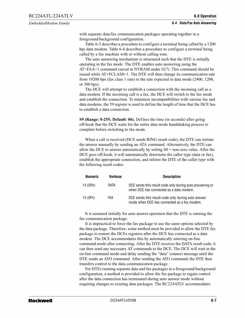
6.0 Operation
6.4 Data/Fax Auto Answering
RC224ATL/224ATLV
EmbeddedModem Family
with separate data/fax communication packages operating together in a foreground/background configuration.
Table 6-3 describes a procedure to configure a terminal being called by a 1200 bps data modem. Table 6-4 describes a procedure to configure a terminal being called by a fax machine with or without calling tone.
The auto answering mechanism is structured such that the DTE is initially operating in the fax mode. The DTE enables auto answering using the AT+FAA=1 command (saved in NVRAM under S27). This command should be issued while AT+FCLASS=1. The DTE will then change its communication rate from 19200 bps (fax class 1 rate) to the rate expected in data mode (2400, 1200, or 300 bps).
The DCE will attempt to establish a connection with the incoming call as a data modem. If the incoming call is a fax, the DCE will switch to the fax mode and establish the connection. To minimize incompatibilities with various fax and data modems, the 59 register is used to define the length of time that the DCE has to establish a data connection.
S9 (Range: 0-255; Default: 06). Defines the time (in seconds) after going off-hook that the DCE waits for the entire data mode handshaking process to complete before switching to fax mode.
When a call is received (DCE sends RING result code), the DTE can initiate the answer manually by sending an ATA command. Alternatively, the DTE can allow the DCE to answer automatically by setting S0 = non-zero value. After the DCE goes off-hook, it will automatically determine the caller type (data or fax), establish the appropriate connection, and inform the DTE of the caller type with the following result codes:
It is assumed initially for auto answer operation that the DTE is running the fax communication package.
It is impractical to force the fax package to use the same options selected by the data package. Therefore, some method must be provided to allow the DTE fax package to restore the DCEs registers after the DCE has connected as a data modem. The DCE accommodates this by automatically entering on-line command mode after connecting. After the DTE receives the DATA result code, it can then send any necessary AT commands to the DCE. The DCE will wait in the on-line command mode and delay sending the “data” connect message until the DTE sends an ATO command. After sending the ATO command, the DTE then transfers control to the data communication package.
For DTEs running separate data and fax packages in a foreground/background configuration, a method is provided to allow the fax package to regain control after the data connection has terminated during auto answer mode without requiring changes to existing data packages. The RC224ATLV accommodates
Numeric Verbose Description
13 (0Dh) DATA DCE sends this result code only during auto answering or when DCE has connected as a data modem.
15 (0Fh) FAX DCE sends this result code only during auto answer mode when DCE has connected as a fax modem.
6-7 D224ATLVDSB

6.0 Operation 6.4 Data/Fax Auto Answering
RC224ATL/224ATLV
EmbeddedModem Family
this through the use of the data carrier detect (DCD) indicator. Initially, in auto answer mode, DCD will be off. When connected in data mode, the DCE will turn DCD on. When the data connection is terminated, the DCE will turn DCD off again. The fax package, running in the background, can poll DCD (160450 modem status register bit 7) to ascertain the data connection status. The DTE must send AT&C1 to cause DCD to operate in this manner.
During auto answer mode, when the caller is a fax machine, the DCE will behave as a normal fax DCE (as defined by +FCLASS=1) with the following exceptions:
1. The transmission of the fax 2100 Hz answer tone will be delayed by the time needed to determine that the caller is a fax machine (S9 seconds).
2. The DCE sends FAX message at the data mode DTE rate (as defined by the previous AT command autobaud rate) and automatically sets +FCLASS=1 after detecting caller is a fax.
3. After the answer tone is sent and the DCE enters the V.21 transmit mode, the CONNECT result code will be sent at 19200.
During auto answer mode, if the DCE determines that the caller is not a data modem nor a fax machine, then DCE will send the NO CARRIER result code, go on-hook and remain in data mode.
6-8 D224ATLVDSB

6.0 Operation
6.5 Call Progress
RC224ATL/224ATLV
EmbeddedModem Family
6.5 Call Progress
6.5.1 Call Progress Algorithms
Data call progress algorithms measure the power and/or relative power of the highband and lowband channels and determine signal presence and cadence correlations. Highband channel signals include 2100 and 2225 Hz signalling tones. Lowband channel signals include dial tones, busy tones, ringback tones and voice ranging in frequency from 120 to 620 Hz.
Characteristics of the tones detected by the RC224ATLV are listed below.
Fax answer tone detection requirements include 2100 and 1100 Hz. The call progress detection requirements are identical to the lowband data signals identified above.
6.5.2 Ring Detection
Ring detection is based on a digital input to the modem. External circuitry not part of the modem is required to convert the analog 40 to 150 VRMS ring signal to a digital single-bit data stream representation. Valid ring frequencies of 15.3 to
Tone Cadence Frequency (Hz)
Dial Tone Continuous 350 + 440
Old Dial Tone Continuous 600+120/133
Busy 0.5 sec ON0.5 sec OFF
480 + 620480 + 620
Old Busy 0.5 sec ON 0.5 sec OFF
600 + 120600 + 120
Precision Reorder 0.3 sec ON 0.2 sec OFF
480 + 620480 + 620
Old Reorder (local) 0.25 sec ON 0.25 sec OFF
600 + 120600 + 120
Old Reorder (toll) 0.2 sec ON 0.3 sec OFF
600 + 120600 + 120
Ringback 0.8-1.2 sec ON 2.7-3.3 OFF
440 + 480440 + 480
Old Ringback 2 sec ON 4 sec OFF
420 + 40420 + 40
Double Ringback 0.8 sec ON 0.3 sec OFF 0.8 sec ON 4 sec OFF
440 + 480 440 + 480 440 + 480 440 + 480
6-9 D224ATLVDSB

6.0 Operation 6.5 Call Progress
RC224ATL/224ATLV
EmbeddedModem Family
68 Hz are detected. Detection is achieved by counting valid high to low ring signal transitions. Valid transitions consist of a high state of 2 to 34 ms followed by a low state of 2 to 42 ms. Ring signals that have transition counts less than the nominal value are discarded.
In addition to valid high to low transitions, ring detection depends on the cadence of the ring ON time (valid transitions occurring) and ring OFF time (no valid transitions). Ring OFF times must be greater than 0.5 seconds. Ring ON times must be greater than 125 ms at 20 Hz (100 ms at 68 Hz).
Ring detection is integrated over 8 seconds. All counters and timers are reset at 8 second intervals. The modem will answer the ring after N valid ON/OFF ring cycles. N is programmable via the SO register. Upon detecting N rings, the modem verifies that the current ring state has been in the OFF state for 0.5 seconds before seizing the line.
Table 6-1. Fax Class 1 Calling Sequence (1 of 2)
DTE Commands (Host)
DCE Responses(Modem) Remote Fax Notes
(1) AT+FCLASS=1 (2) OK Set to Class 1
PHASE A
(3) ATDT6163 (4) dials(6) CONNECT
(5) answers(7) Send HDLC flags
+FRH=3 implied by Dialing
PHASE B
(8) Send NSF Frame
(9) <NSF>, OK
(10) AT+FRH=3 (11) CONNECT
(12) Send CSI frame
(13) <CIS>, OK
(14) AT+FRH=3 (15) CONNECT
(16) Send DIS frame last frame bit = 1
(17) <DIS>, OK (18) Drop carrier
(19) AT+FTH=3 (20) send HDLC flags (21) Receive flags
(21) CONNECT
(22) <TSI> (23) Send TSI frame (24) Receive TSI last frame bit = 0
(25) CONNECT
(26) <DCS> (27) send DCS frame (28) Received DCS last frame bit = 1
(29) detect last frame bit
(30) OK, drop carrier
(31) AT+FTS=8 (32) OK, wait 80 ms
6-10 D224ATLVDSB
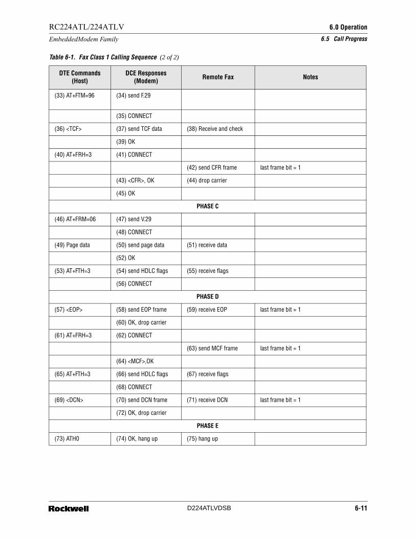
6.0 Operation
6.5 Call Progress
RC224ATL/224ATLV
EmbeddedModem Family
(33) AT+FTM=96 (34) send F.29
(35) CONNECT
(36) <TCF> (37) send TCF data (38) Receive and check
(39) OK
(40) AT+FRH=3 (41) CONNECT
(42) send CFR frame last frame bit = 1
(43) <CFR>, OK (44) drop carrier
(45) OK
PHASE C
(46) AT+FRM=06 (47) send V.29
(48) CONNECT
(49) Page data (50) send page data (51) receive data
(52) OK
(53) AT+FTH=3 (54) send HDLC flags (55) receive flags
(56) CONNECT
PHASE D
(57) <EOP> (58) send EOP frame (59) receive EOP last frame bit = 1
(60) OK, drop carrier
(61) AT+FRH=3 (62) CONNECT
(63) send MCF frame last frame bit = 1
(64) <MCF>,OK
(65) AT+FTH=3 (66) send HDLC flags (67) receive flags
(68) CONNECT
(69) <DCN> (70) send DCN frame (71) receive DCN last frame bit = 1
(72) OK, drop carrier
PHASE E
(73) ATH0 (74) OK, hang up (75) hang up
Table 6-1. Fax Class 1 Calling Sequence (2 of 2)
DTE Commands (Host)
DCE Responses(Modem) Remote Fax Notes
6-11 D224ATLVDSB

6.0 Operation 6.5 Call Progress
RC224ATL/224ATLV
EmbeddedModem Family
Table 6-2. Fax Class 1 Answering Sequence (1 of 2)
DTE Commands (Host)
DCE Responses (Modem) Remote Fax Notes
(1) AT+FCLASS=1 (2) OK Set to Class 1
(2b) AT+FRM=? 24,48
OK
PHASE A
(3) FAX machine dials
(4) RING
(5) ATA (6) modem answers
(7) Send HDLC flags (8) Receive flags +FTH=3 implied by answering
(9) CONNECT
PHASE B
(10) <NSF> (11) send NSF frame (12) Receive NSF last frame bit = 0
(13) CONNECT
(14) <CSI> (15) send CSI frame (16) Receive CSI last frame bit = 0
(17) CONNECT
(18) <DSI> (19) send DSI frame (20) Receive DSI last frame bit = 1
(21) OK, drop carrier
(22) AT + FRH=3 (23) CONNECT
(24) Send TSI frame last frame bit = 0
(25) <TSI>,OK
(26) AT+FRH=3 (27) CONNECT
(28) send DCS frame last frame bit = 1
(29) <DCS>,OK (30) Drop Carrier
(31) AT+FTH=3
(32) Send V.27 (4800)
(33) CONNECT (34) Send TCF frame
(35) <TCF> (36) Drop Carrier
(37) NO CARRIER
(38) AT+FRM=48 (39) CONNECT
(40) <CFR> (41) Send CFR frame (42) Receive CFR last frame bit = 1
(43) OK, drop carrier
6-12 D224ATLVDSB
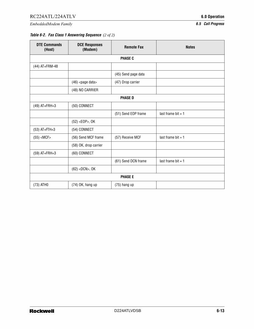
6.0 Operation
6.5 Call Progress
RC224ATL/224ATLV
EmbeddedModem Family
PHASE C
(44) AT+FRM-48
(45) Send page data
(46) <page data> (47) Drop carrier
(48) NO CARRIER
PHASE D
(49) AT+FRH=3 (50) CONNECT
(51) Send EOP frame last frame bit = 1
(52) <EOP>, OK
(53) AT+FTH=3 (54) CONNECT
(55) <MCF> (56) Send MCF frame (57) Receive MCF last frame bit = 1
(58) OK, drop carrier
(59) AT+FRH=3 (60) CONNECT
(61) Send DCN frame last frame bit = 1
(62) <DCN>, OK
PHASE E
(73) ATH0 (74) OK, hang up (75) hang up
Table 6-2. Fax Class 1 Answering Sequence (2 of 2)
DTE Commands (Host)
DCE Responses (Modem) Remote Fax Notes
6-13 D224ATLVDSB

6.0 Operation 6.5 Call Progress
RC224ATL/224ATLV
EmbeddedModem Family
Table 6-3. Terminal Called by a 1200 bps Data Modem
DTE Command DCE Response Comments
Assume DCE in fax mode (FCLASS = 1), DTE running fax communication package, and DCD is off.
AT&C1 OK DTE commands DCD to follow data carrier.
ATS9=n OK DTE defines the data mode connection time.
AT+FAA=1 OK DTE enables data/fax auto answer mode.
DTE sets the communication rate to the data modem rate (e.g., 2400 bps) prior to an incoming call.
RING Terminal is being called.
ATA DTE commands DCE to go off-hook and start auto answer.
DCE determines caller as data modem and establishes connection with caller.
DCE turns on DCD to indicate data connection is established.
DCE then waits in on-line command mode.
DATA DCE indicates data modem connection is established.
AT commands OK DTE optionally sends any commands to DCE to restore conditions required by data modem communications package.
ATO CONNECT 1200 DTE instructs DCE to switch from on-line command to data state.
DTE then transfers control to data modem package.
Fax package remains in background polling DCD to check connection status.
DCE response will then be read by data modem communication rate to 1200 bps.
“Callers data” DTE sends/receives data.
Caller hangs up. DTE detects carrier loss and turns off DCD.
NO CARRIER DCE indicates connection with caller has terminated.
DTE fax communications software, running in background, sees DCD turn off, and regains control from data modem package.
6-14 D224ATLVDSB

6.0 Operation
6.5 Call Progress
RC224ATL/224ATLV
EmbeddedModem Family
Table 6-4. Terminal Called by a Fax Machine
DTE Command DCE Response Comments
Assume DCE in fax mode (FCLASS = 1), DTE is running fax communication package, and DCD is off.
AT&C1 OK DTE commands DCD to follow data carrier.
ATS9=n OK DTE defines the data mode connection time.
AT+FAA=1 OK DTE enables data/fax auto answer mode.
DTE sets the communication rate to the data modem rate (e.g., 2400 bps) prior to an incoming call.
RING Terminal is being called.
ATA DTE commands DCE to go off-hook and start auto answer.
DCE starts data modem handshaking. If receive data signal is not detected within S9 seconds from going off-hook, DCE switches to fax mode and automatically sets FCLASS=1.
FAX DCE switches to fax mode handshaking and sends “FAX” message at the data modem rate (e.g., 2400 bps).
DCE sends 3 seconds of 2100 Hz answer tone, enters V.21 transmit mode, and sends HDLC flags.
CONNECT DCE ends CONNECT response at the fax rate (i.e., 19200 bps).
6-15 D224ATLVDSB

6.0 Operation 6.5 Call Progress
RC224ATL/224ATLV
EmbeddedModem Family
6-16 D224ATLVDSB

7.0 Electrical/Mechanical Specifications
7.1 Interfacing the RC224ATLV
7.1.1 Interfacing the RC224ATLV 3.3 V Digital Logic with External 5.0 V Digital Logic
The RC224ATLV is not 5.0 V I/O logic tolerant. It is recommended to add a series resistor of 150 ohms to current limit the digital inputs to the RC224ATLV when interfacing to +5.0 V logic output lines. The digital outputs of the RC224ATLV should not go to resistor pull-ups that are connected to the +5 V power supply. These precautions will help prevent the modem chip from going into latch-up due to raising any input or output pin level more than +0.3 V above the +3.3 V power rail of the RC224ATLV.
7.2 Environmental Requirements
The environmental specifications are listed in Table 7-1.
7.3 Interface Timing and Waveforms
Table 7-2 lists the host bus interface timing parameters. Figure 7-1 illustrates the interface waveforms.
Table 7-1. Environmental Specifications
Parameter Specification
Operating Temperature 0°C to +70°C (32°F to 158°F)
Storage Temperature -55°C to +125°C (-67°F to +257°F)
Relative Humidity Up to 90% noncondensing, or a wet bulb temperature up to 35°C, whichever is less.
7-1 D224ATLVDSB

7.0 Electrical/Mechanical Specifications 7.3 Interface Timing and Waveforms
RC224ATL/224ATLV
EmbeddedModem Family
Table 7-2. Timing - Host Bus Interface
Symbol Parameter Min Max Units
tAS Address Setup 25 - ns
tAH Address Hold 0 - ns
tCS Chip Select Setup 10 - ns
tCH Chip Select Hold 0 - ns
tRD Read Strobe Width 100 - ns
tDD Delay HRD to Data - 75 ns
tDRH HRD to Data Hold 10 - ns
tWT Write Strobe Width 75 - ns
tDS Write Data Setup 30 - ns
tDWH Write Data Hold 10 - ns
tDF HRD to Driver Off - 30 ns
tDIS HDIS Enable - 40 ns
tDIH HDIS Hold 40 - ns
tINH Interrupt Hold - 100 ns
7-2 D224ATLVDSB

7.0 Electrical/Mechanical Specifications
7.3 Interface Timing and Waveforms
RC224ATL/224ATLV
EmbeddedModem Family
Figure 7-1. Timing Waveform
tDDtDIHtDIS
tRD
tDF
tDRH
tAS
tCS tCH
tAH
HA0-HA2
HCS
HRD
HWT
HD0-HD7
HDIS
a. Host Read
tDS
tWT
tDWH
tAS
tCS tCH
tAH
HA0-HA2
HCS
HRD
HWT
HD0-HD7
HDIS
b. Host Write
7-3 D224ATLVDSB
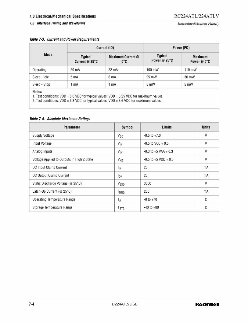
7.0 Electrical/Mechanical Specifications 7.3 Interface Timing and Waveforms
RC224ATL/224ATLV
EmbeddedModem Family
Table 7-3. Current and Power Requirements
Mode
Current (ID) Power (PD)
TypicalCurrent @ 25°C
Maximum Current @ 0°C
TypicalPower @ 25°C
MaximumPower @ 0°C
Operating 20 mA 22 mA 100 mW 110 mW
Sleep - Idle 5 mA 6 mA 25 mW 30 mW
Sleep - Stop 1 mA 1 mA 5 mW 5 mW
Notes:1. Test conditions: VDD = 5.0 VDC for typical values; VDD = 5.25 VDC for maximum values.2. Test conditions: VDD = 3.3 VDC for typical values; VDD = 3.6 VDC for maximum values.
Table 7-4. Absolute Maximum Ratings
Parameter Symbol Limits Units
Supply Voltage VDD -0.5 to +7.0 V
Input Voltage VIN -0.5 to VCC + 0.5 V
Analog Inputs VIN -0.3 to +5 VAA + 0.3 V
Voltage Applied to Outputs in High Z State VHZ -0.5 to +5 VDD + 0.5 V
DC Input Clamp Current IIK 20 mA
DC Output Clamp Current IOK 20 mA
Static Discharge Voltage (@ 25°C) VESD 3000 V
Latch-Up Current (@ 25°C) ITRIG 200 mA
Operating Temperature Range TA -0 to +70 C
Storage Temperature Range TSTG -40 to +80 C
7-4 D224ATLVDSB

7.0 Electrical/Mechanical Specifications
7.3 Interface Timing and Waveforms
RC224ATL/224ATLV
EmbeddedModem Family
Table 7-5. Digital Interface Characteristics
Parameter Symbol Min. Typ. Max Units Test Conditions1
Input High VoltageType IAType DIOType IH
VIH2.02.4-30
---
VCCVCC30
Vdc
Input Low VoltageType IA, IC, and DO
VIL-0.3 - 0.8
Vdc
Input Low VoltageType IF
VIL38 - -
VrmsNote 3
Input Leakage CurrentIA and IC
IIN- - 10
µAdc VIN = 0 to VCC
Output High VoltageType OAType ODType OGType OH
VOH2.4--5
---8
-VCCVCC-
VdcILOAD = -100 µAILOAD = 0 mA
Output Low VoltageType OAType OBType ODType OGType OH
VOL---0.5-8
--0.75--5
0.40.4---
VdcILOAD = 1.6 mAILOAD = 0.8 mAILOAD = 15 mAILOAD = 8 mA
Three-State (off) Current ITS 25 µAdc VIN = 0.8 V to 4.5 V
Notes:1. Test Conditions: VCC = 5 V 5%, TA= 0°C to 70°C (unless otherwise stated). (RC224ATL)
Test Conditions: VCC = 3.3 V 5%, TA= 0°C to 70°C (unless otherwise stated). (RC224ATLV)2. Output loads: 50 pF + one TTL.3. AC Vrms voltage between Tip and Ring, using the on-board modular DAA.
7-5 D224ATLVDSB
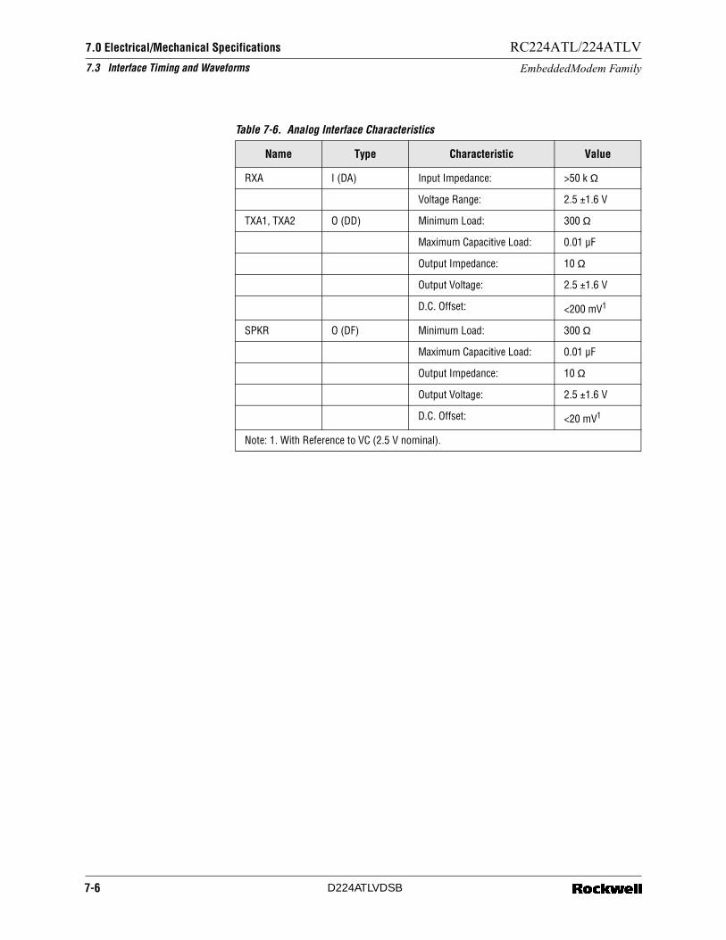
7.0 Electrical/Mechanical Specifications 7.3 Interface Timing and Waveforms
RC224ATL/224ATLV
EmbeddedModem Family
Table 7-6. Analog Interface Characteristics
Name Type Characteristic Value
RXA I (DA) Input Impedance: >50 k Ω
Voltage Range: 2.5 ±1.6 V
TXA1, TXA2 O (DD) Minimum Load: 300 Ω
Maximum Capacitive Load: 0.01 µF
Output Impedance: 10 Ω
Output Voltage: 2.5 ±1.6 V
D.C. Offset: <200 mV1
SPKR O (DF) Minimum Load: 300 Ω
Maximum Capacitive Load: 0.01 µF
Output Impedance: 10 Ω
Output Voltage: 2.5 ±1.6 V
D.C. Offset: <20 mV1
Note: 1. With Reference to VC (2.5 V nominal).
7-6 D224ATLVDSB
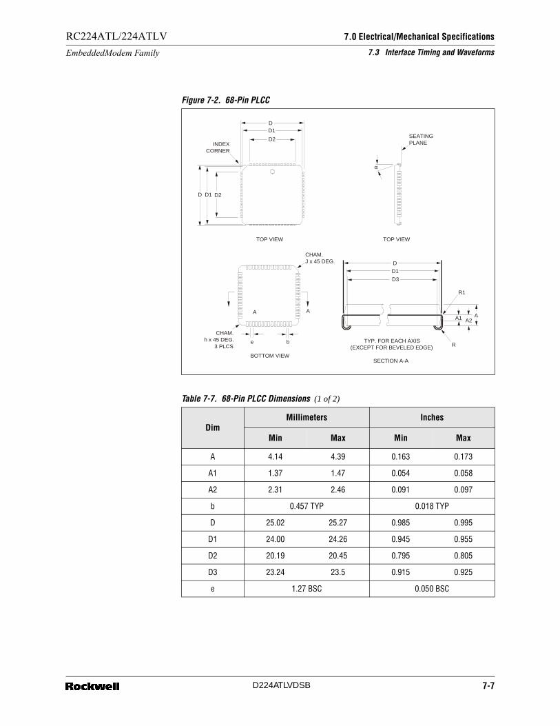
7.0 Electrical/Mechanical Specifications
7.3 Interface Timing and Waveforms
RC224ATL/224ATLV
EmbeddedModem Family
Figure 7-2. 68-Pin PLCC
D D1 D2
DD1
D2
D
D1
D3
INDEX CORNER
TOP VIEW TOP VIEW
BOTTOM VIEW
TYP. FOR EACH AXIS (EXCEPT FOR BEVELED EDGE)
SECTION A-A
AA
be
CHAM. h x 45 DEG.
3 PLCS
CHAM. J x 45 DEG.
SEATING PLANE
R1
R
AA1 A2
α
Table 7-7. 68-Pin PLCC Dimensions (1 of 2)
DimMillimeters Inches
Min Max Min Max
A 4.14 4.39 0.163 0.173
A1 1.37 1.47 0.054 0.058
A2 2.31 2.46 0.091 0.097
b 0.457 TYP 0.018 TYP
D 25.02 25.27 0.985 0.995
D1 24.00 24.26 0.945 0.955
D2 20.19 20.45 0.795 0.805
D3 23.24 23.5 0.915 0.925
e 1.27 BSC 0.050 BSC
7-7 D224ATLVDSB
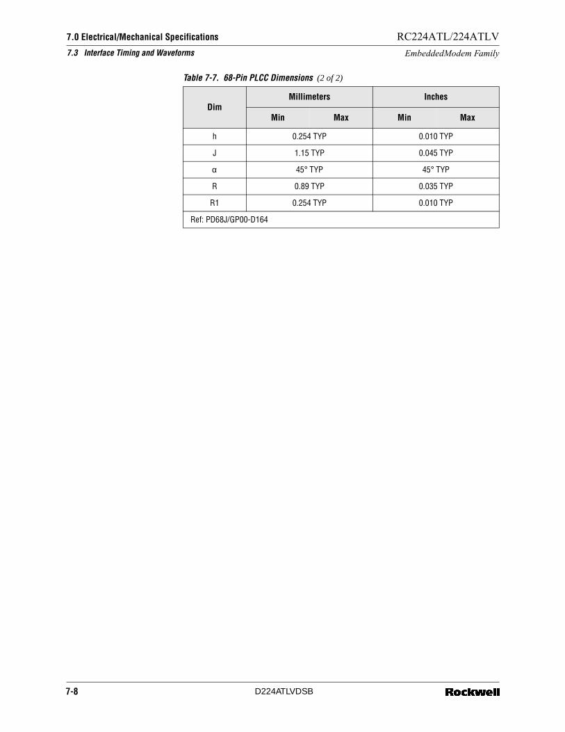
7.0 Electrical/Mechanical Specifications 7.3 Interface Timing and Waveforms
RC224ATL/224ATLV
EmbeddedModem Family
h 0.254 TYP 0.010 TYP
J 1.15 TYP 0.045 TYP
α 45° TYP 45° TYP
R 0.89 TYP 0.035 TYP
R1 0.254 TYP 0.010 TYP
Ref: PD68J/GP00-D164
Table 7-7. 68-Pin PLCC Dimensions (2 of 2)
DimMillimeters Inches
Min Max Min Max
7-8 D224ATLVDSB

7.0 Electrical/Mechanical Specifications
7.3 Interface Timing and Waveforms
RC224ATL/224ATLV
EmbeddedModem Family
Figure 7-3. 100-Pin PQFP
D D1 E1
D
D1
TOP VIEW SIDE VIEW
DETAIL A
baPIN 1REF
SeeDetail ACHAM.
H x 45 DEG.(4x)
R1
R2
AA1
K1A2 K2
K3
J
Table 7-8. 100-Pin PQFP Dimensions (1 of 2)
DimMillimeters Inches
Min Max Min Max
A 1.95 2.05 0.077 0.081
A1 0.95 1.05 0.037 0.041
A2 0.15 0.25 0.006 0.010
D 22.96 23.44 0.904 0.923
D1 19.89 20.09 0.783 0.791
E 16.94 17.45 0.667 0.687
E1 13.89 14.10 0.547 0.555
K1 0.70 0.90 0.028 0.035
K2 0.40 – 0.016 –
K3 1.60 REF 0.083 REF
R1 0.13 – 0.005 –
7-9 D224ATLVDSB

7.0 Electrical/Mechanical Specifications 7.3 Interface Timing and Waveforms
RC224ATL/224ATLV
EmbeddedModem Family
R2 0.15 0.25 0.008 0.010
a 0.60 0.70 0.024 0.028
b 0.26 0.36 0.010 0.014
H – 0.25 – 0.010
J 0.13 0.17 0.005 0.007
Ref: GP00-D234
Table 7-8. 100-Pin PQFP Dimensions (2 of 2)
DimMillimeters Inches
Min Max Min Max
7-10 D224ATLVDSB
Appendix A. Modem Designs
A.1 RC224ATF Modem Designs
This appendix describes two modem design examples. The schematics and parts lists are provided for designs incorporating the RC224ATF packaged in a 68-pin PLCC and implemented with either a parallel or serial interface.
A.1.1 RC224ATF 68-Pin PLCC Design for Serial Interface
Figure A-1 and Figure A-2 provides the schematic of a RC224ATF 68-pin PLCC serial interface board design.Table A-1 is the parts list of a RC224ATF 68-pin PLCC serial interface board design.
A-1 D224ATLVDSB
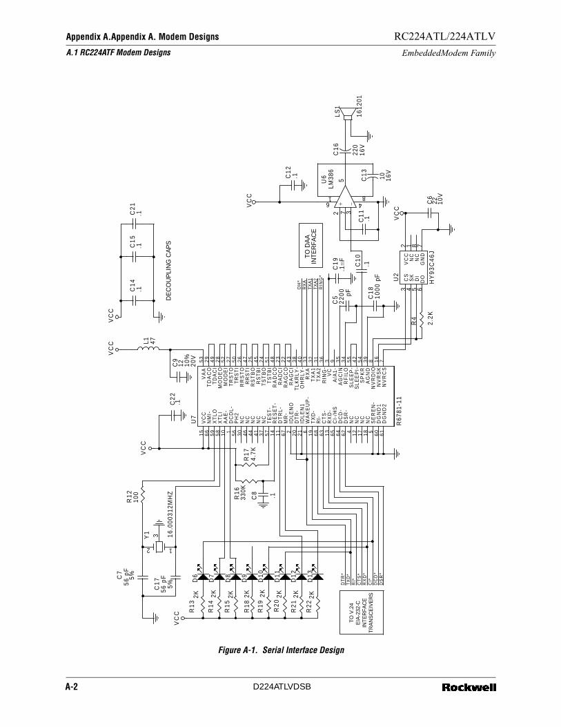
Appendix A.Appendix A. Modem Designs A.1 RC224ATF Modem Designs
RC224ATL/224ATLV
EmbeddedModem Family
Figure A-1. Serial Interface Design
DE
CO
UP
LIN
G C
AP
S
TO V
.24
EIA
-232
-CIN
TER
FAC
ETR
AN
SC
EIV
ER
S
TO D
AA
INTE
RFA
CE
OH
*
TXA
2TX
A1
RX
A
DT
R*
RI*
CT
S*
DS
R*
RX
D*
CI*
DC
D*
TX
D*
RIN
G*
VC
C
VC
C
VC
C
VC
CV
CC
VC
C
C5
22
00
pF
R4
2.2K
C1
0.1
C1
1.1
C1
3
10 16V
LS1
1612
01
L1 47
C1
81
00
0 p
F
C1
9.1m
F
C6
22 10V
C7
56
pF
5%
C1
75
6 p
F5%
Y1 16
.000
312M
HZ
12
3
C1
4.1
+ -
U6
LM38
62 3
5
61
48
7
U2
HY
93
C4
6J
3 5
2 84 6
71C
S
DI
VC
C
NC
SK
DO
GN
D
NC
C1
6
220
16V
C1
5.1
C1
2.1
C2
2.1
C9
12 10%
20V
C2
1.1
R1
74.
7K
U7
R67
81-1
1
15
66
59
58
10 1 56
30
46
44
41
37
57
14
11
67 2 20
21 6 19
68
63
13
65
64
62 4 12
17
18 5 60
61
53
29
49
28
52
27
50
26
47
25
45
24
51
48
23
22
43
38
40
33
32
31
36
3 9 35
34
55
42
54
39
8 16
7
VC
CN
MI-
XT
LO
XT
LIA
AE
-D
CD
L-
PH
2N
CN
CN
CN
CN
CT
ES
T-
RE
SE
T-
DT
RL
-M
R-
IDL
EN
OD
TR
-ID
LE
N1
WA
KE
UP
-T
XD
-R
I-C
TS
-R
XD
-C
I-/H
SD
CD
-D
SR
-N
CN
CN
CN
CS
ER
EN
-D
GN
D1
DG
ND
2
VA
AT
DA
CO
TD
AC
IM
OD
EO
MO
DE
IT
RS
TO
TR
ST
IR
RS
TO
RR
ST
IR
ST
BO
RS
TB
IT
ST
BO
TS
TB
IR
AD
CO
RA
DC
IR
AG
CO
RA
GC
IT
LK
RL
Y-
OH
RL
Y-
RX
AT
XA
1T
XA
2
VC
RIN
G-
A/A
1-
AG
CIN
RF
ILO
SL
EE
P-
SL
EE
PI-
SP
KR
AG
ND
NV
RD
ION
VR
SK
NV
RC
S
R1
32K
D6
R
14
2KD
7
R
15
2KD
8
R
18
2KD
9
R
19
2KD
10
R
20
2KD
11
R
21
2KD
12
R
22
2KD
13
R1
633
0K
C8 .1
R1
210
0
A-2 D224ATLVDSB

Appendix A.Appendix A. Modem Designs
A.1 RC224ATF Modem Designs
RC224ATL/224ATLV
EmbeddedModem Family
Figure A-2. Serial Interface Design DAA
OH
*
TXA
1
TXA
2
RIN
G*
RX
A
VC
C
VC
C
R1
18 1W
RV
1V
150L
A2
TOP
J4 TE
LC
O4/
61 2 3 4 5 68 7
R2
7.5K
1W D
11
N97
0B
D2
1N
970B
LIN
E
T1 TT
C14
3
K1
RE
LA
Y
14 2 3
C4
.01
D5
1N
749A
R3
100K
R6
536
1%
R9
1.5K
D4
1N
749A
C2
0.1
U1
4N
35
645
132
D3
1N
4148
R1
1
0
R1
0
0
C2
.001
10%
1KV
C3
.47
10%
250V
C1
.001
10%
1KV
TOP
J3 TE
LC
O4/
61 2 3 4 5 68 7
A-3 D224ATLVDSB

Appendix A.Appendix A. Modem Designs A.1 RC224ATF Modem Designs
RC224ATL/224ATLV
EmbeddedModem Family
A.1.2 Serial Bill Of Materials
Table A-1. Serial Bill of Materials (1 of 2)
Item Quantity Reference Part
1 2 C2,C1 0.001
2 1 C3 0.47
3 1 C4 .01
4 1 C5 2200 pF
5 1 C6 22
6 2 C7,C17 56 pF
7 9 C8,C10,C11,C12,C14,C15,C19, C20,C21
0.1
8 1 C9 12
9 1 C13 10
10 1 C16 220
11 1 C18 1000 pF
12 2 D1,D2 1N970B
13 1 D3 1N4148
14 2 D5,D4 1N749A
15 8 D6,D7,D8,D9,D10,D11,D12,D13
16 2 J4,J3 TELCO4/6
17 1 K1 RELAY
18 1 LS1 161201
19 1 L1 47
20 1 RV1 V150LA2
21 1 R1 18
22 1 R2 7.5 k
23 1 R3 100 k
24 1 R4 2.2 k
25 1 R6 536
26 1 R9 1.5 k
27 2 R11,R10 0
28 1 R12 100
A-4 D224ATLVDSB

Appendix A.Appendix A. Modem Designs
A.1 RC224ATF Modem Designs
RC224ATL/224ATLV
EmbeddedModem Family
29 8 R13,R14,R15,R18,R19,R20,R21,R22
2 k
30 1 R16 330 k
31 1 R17 4.7 k
32 1 T1 TTC143
33 1 U1 4N35
34 1 U2 HY93C46J
35 1 U6 LM386
36 1 U7 R6781-11
37 1 Y1 16.000312 MHz
Table A-1. Serial Bill of Materials (2 of 2)
Item Quantity Reference Part
A-5 D224ATLVDSB

Appendix A.Appendix A. Modem Designs A.2 RC224ATF 68-Pin PLCC Design for Parallel Interface
RC224ATL/224ATLV
EmbeddedModem Family
A.2 RC224ATF 68-Pin PLCC Design for Parallel Interface
Figure A-3 and Figure A-4 provides the schematic of a RC224ATF 68-pin PLCC parallel interface board design.
Table A-2 is the parts list of a RC224ATF 68-pin PLCC parallel interface board design.
A-6 D224ATLVDSB
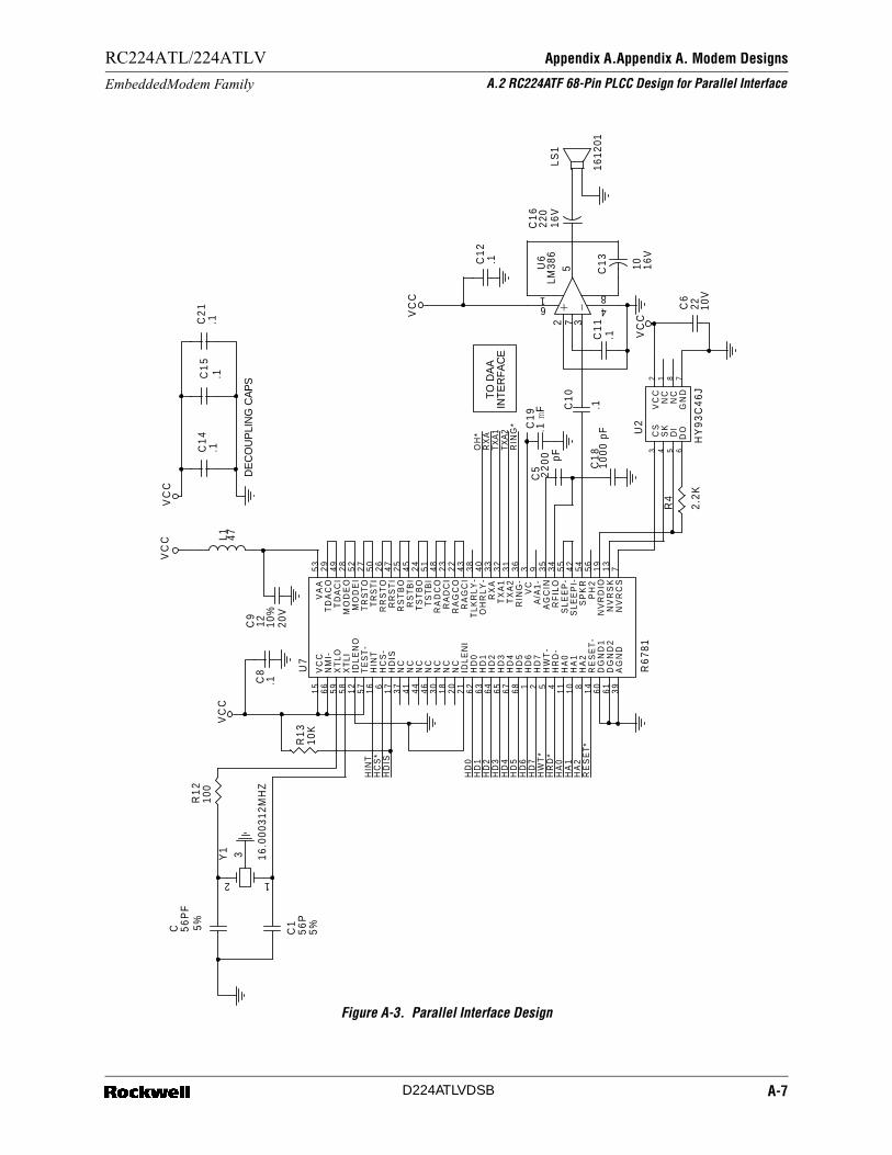
Appendix A.Appendix A. Modem Designs
A.2 RC224ATF 68-Pin PLCC Design for Parallel Interface
RC224ATL/224ATLV
EmbeddedModem Family
Figure A-3. Parallel Interface Design
DE
CO
UP
LIN
G C
AP
S
TO D
AA
INTE
RFA
CE
HC
S*
HD
IS
OH
*
TXA
2R
ING
*
HW
T*
HR
D*
HA
0H
A1
HA
2R
ES
ET
*
HIN
T
HD
0H
D1
HD
2H
D3
HD
4H
D5
HD
6H
D7
TXA
1R
XA
VC
C
VC
C
VC
C
VC
CV
CC
C5 22
00
pF
R4
2.2K
C1
0
.1C
11
.1C
13
10 16V
L1 47
C6
22 10V
C 56
PF
5% C1
56
P5%
C1
4.1
+ -
U6
LM38
62 3
5
61
48
7
U2
HY
93
C4
6J
3 5
2 84 6
71C
S
DI
VC
C
NC
SK
DO
GN
D
NC
C1
5.1
C8
.1
C9
12 10%
20V
C2
1.1
R1
310
KU
7
R6
781
15
66
59
58
12
57
16 6 17
37
41
44
46
30
18
20
21
62
63
64
65
67
68 1 2 5 4 11
10 8 14
60
61
39
53
29
49
28
52
27
50
26
47
25
45
24
51
48
23
22
43
38
40
33
32
31
36
3 9 35
34
55
42
54
56
19
13
7
VC
CN
MI-
XT
LO
XT
LIID
LE
NO
TE
ST
-H
INT
HC
S-
HD
ISN
CN
CN
CN
CN
CN
CN
CID
LE
NI
HD
0H
D1
HD
2H
D3
HD
4H
D5
HD
6H
D7
HW
T-
HR
D-
HA
0H
A1
HA
2R
ES
ET
-D
GN
D1
DG
ND
2A
GN
D
VA
AT
DA
CO
TD
AC
IM
OD
EO
MO
DE
IT
RS
TO
TR
ST
IR
RS
TO
RR
ST
IR
ST
BO
RS
TB
IT
ST
BO
TS
TB
IR
AD
CO
RA
DC
IR
AG
CO
RA
GC
IT
LK
RL
Y-
OH
RL
Y-
RX
AT
XA
1T
XA
2
VC
RIN
G-
A/A
1-
AG
CIN
RF
ILO
SL
EE
P-
SL
EE
PI-
SP
KR
PH
2N
VR
DIO
NV
RS
KN
VR
CS
C1
9.1
mF
R1
210
0
C1
622
016
V
C1
81
00
0 p
F
C1
2.1
Y1
16
.000
312M
HZ
12
3
LS1
1612
01
A-7 D224ATLVDSB
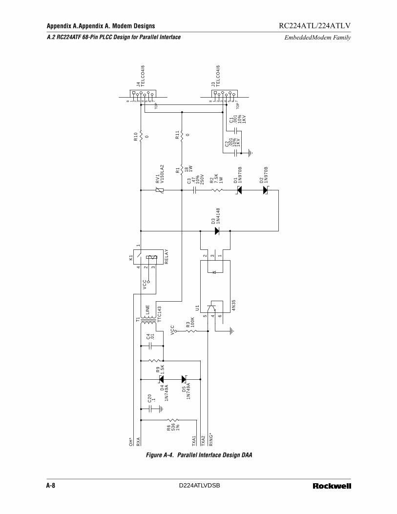
Appendix A.Appendix A. Modem Designs A.2 RC224ATF 68-Pin PLCC Design for Parallel Interface
RC224ATL/224ATLV
EmbeddedModem Family
Figure A-4. Parallel Interface Design DAA
OH
*
TXA
1
TXA
2
RIN
G*
RX
A
VC
C
VC
C
R1 18 1W
RV
1V
150L
A2
TOP
J4 TE
LC
O4/
6
1 2 3 4 5 68 7
R2
7.5K
1W D1
1N
970B
D2
1N
970B
LIN
E
T1 TT
C14
3
K1
RE
LA
Y
14 2 3
C4
.01
D5
1N
749A
R3
100K
R6
536
1%
R9
1.5K
D4
1N
749A
C2
0.1
U1
4N
35
645
132
D3
1N
4148
R1
1
0
R1
0
0
C2
.001
10%
1KV
C3
.47
10%
250V
C1
.001
10%
1KV
TOP
J3 TE
LC
O4/
61 2 3 4 5 68 7
A-8 D224ATLVDSB
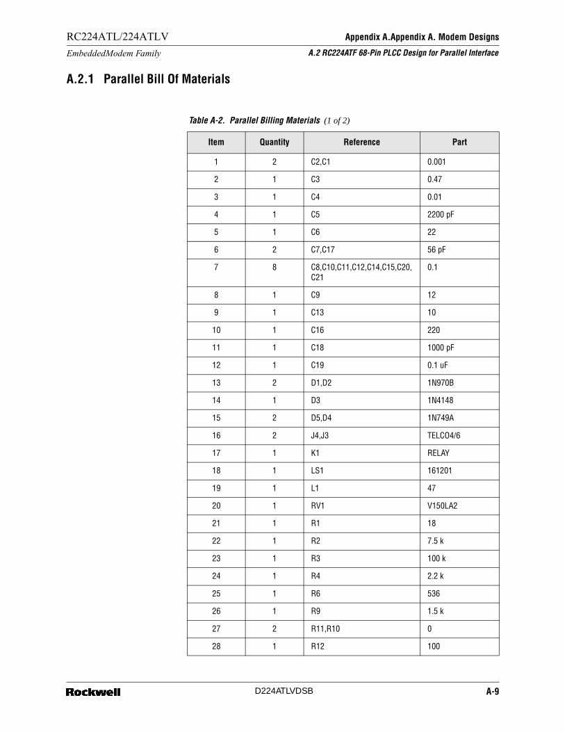
Appendix A.Appendix A. Modem Designs
A.2 RC224ATF 68-Pin PLCC Design for Parallel Interface
RC224ATL/224ATLV
EmbeddedModem Family
A.2.1 Parallel Bill Of Materials
Table A-2. Parallel Billing Materials (1 of 2)
Item Quantity Reference Part
1 2 C2,C1 0.001
2 1 C3 0.47
3 1 C4 0.01
4 1 C5 2200 pF
5 1 C6 22
6 2 C7,C17 56 pF
7 8 C8,C10,C11,C12,C14,C15,C20,C21
0.1
8 1 C9 12
9 1 C13 10
10 1 C16 220
11 1 C18 1000 pF
12 1 C19 0.1 uF
13 2 D1,D2 1N970B
14 1 D3 1N4148
15 2 D5,D4 1N749A
16 2 J4,J3 TELCO4/6
17 1 K1 RELAY
18 1 LS1 161201
19 1 L1 47
20 1 RV1 V150LA2
21 1 R1 18
22 1 R2 7.5 k
23 1 R3 100 k
24 1 R4 2.2 k
25 1 R6 536
26 1 R9 1.5 k
27 2 R11,R10 0
28 1 R12 100
A-9 D224ATLVDSB
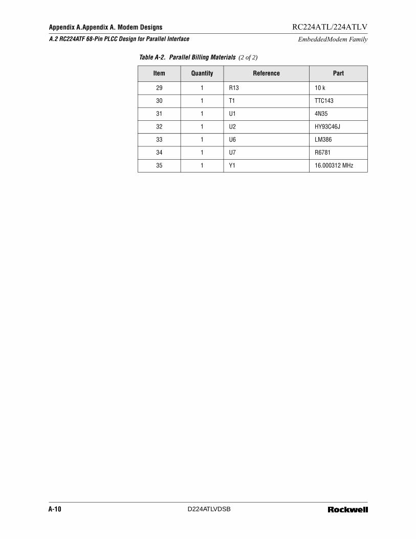
Appendix A.Appendix A. Modem Designs A.2 RC224ATF 68-Pin PLCC Design for Parallel Interface
RC224ATL/224ATLV
EmbeddedModem Family
29 1 R13 10 k
30 1 T1 TTC143
31 1 U1 4N35
32 1 U2 HY93C46J
33 1 U6 LM386
34 1 U7 R6781
35 1 Y1 16.000312 MHz
Table A-2. Parallel Billing Materials (2 of 2)
Item Quantity Reference Part
A-10 D224ATLVDSB


WORLDWIDE HEADQUARTERS
Rockwell Semiconductor Systems4311 Jamboree RoadP.O. Box CNewport Beach, CA 92658-8902
Phone: (949) 221-4600Fax: (949) 221-6375
US South CentralPhone: (972) 733-0723Fax: (972) 407-0639
Phone: (281) 807-5553Fax: (281) 955-2913
US NortheastPhone: (978) 692-7660Fax: (978) 692-8185
EUROPE
European HeadquartersRockwell SemiconductorSystems S.A.SLes Taissounieres B11680 Route des DolinesBP 28306905 Sophia Antipolis Cedex, FrancePhone: (33-4) 93 00 33 35Fax: (33-4) 93 00 33 03
APAC
APAC HeadquartersRockwell Int’l ManufacturingPte Ltd.1 Kim Seng Promenade#09-01 East TowerGreat World CitySingapore 237994Phone: (65) 737-7355Fax: (65) 737-9077
TAIWAN
Taiwan HeadquartersRockwell Int’l TaiwanCompany, Ltd.Room 2808 InternationalTrade Bldg.333 Keelung Road, Section ITaipei, Taiwan10548 ROCPhone: (886-2) 2-720-0282Fax: (886-2) 2-757-6760
Web:www.rss.rockwell.com
AMERICAS
US Northwest/Pacific NorthwestPhone: (408) 249-9696Fax: (408) 249-7113
US Los AngelesPhone: (805) 376-0559Fax: (805) 376-8180
US SoutheastPhone: (770) 246-8283Fax: (770) 246-0018
Phone: (919) 786-4002Fax: (919) 782-8727
US FloridaPhone: (727) 799-8406Fax: (727) 799-8306
Europe CentralPhone: (49-89) 829-1320Fax: (49-89) 834-2734
Europe Mediterranean (Satellite)RSS c/o Rockwell Automation S.r.l.Phone: (34-91) 565 16 16Fax: (34-91) 565 16 87
Europe MediterraneanPhone: (39-2) 93179911Fax: (39-2) 93179913
Europe NorthPhone: (44-1344) 486 444Fax: (44-1344) 486 555
Europe SouthPhone: (33-1) 49 06 39 80Fax: (33-1) 49 06 39 90
Europe IsraelPhone: (972-9) 9524 000Fax: (972-9) 9573 732
AustraliaPhone: (61-2) 9869 4088Fax: (61-2) 9869 4077
JAPAN
Japan HeadquartersRockwell Int’l Japan Co. Ltd.Shimomoto Bldg.1-46-3 Hatsudai, Shibuya-kuTokyo, 151 JapanPhone: (81-3) 5371 1520Fax: (81-3) 5371 1501
Email:[email protected]
ChinaPhone: (86-21) 6361-2515Fax: (86-21) 6361-2516
For more information:Call 1-800-854-8099
US San DiegoPhone: (619) 535-3374Fax: (619) 452-1249
South AmericaPhone: 55 11 3874 8978Fax: 55 11 3874 8883
Hong KongPhone: (852) 2 827-0181Fax: (852) 2 827-6488
International Information:Call 1-714-221-6996
US SouthwestPhone: (949) 222-9119Fax: (949) 222-0620
US Mid-AtlanticPhone: (215) 244-6784Fax: (215) 244-9292
IndiaPhone: (91-11) 692-4780Fax: (91-11) 692-4712
Document Number:
D224ATLVDSB
US North CentralPhone: (630) 773-3454Fax: (630) 773-3907
Europe North (Satellite)Phone: (46) 8 477 4036Fax: (46) 8 477 4037
KoreaPhone: (82-2) 565-2880Fax: (82-2) 565-1440
Related Documents