Applied Surface Science 279 (2013) 23–30 Contents lists available at SciVerse ScienceDirect Applied Surface Science j ourna l ho me page: www.elsevier.com/locate/apsusc Rapid thermal annealing effects on the microstructure and the thermoelectric properties of electrodeposited Bi 2 Te 3 film Mohammad Mamunur Rashid a , Kyung Ho Cho b , Gwiy-Sang Chung a,∗ a School of Electrical Engineering, University of Ulsan, 93 Daehak-ro, Nam-gu, Ulsan 680-749, Republic of Korea b Agency for Defense Development, Yuseong P.O. Box 35-42, Daejeon 305-600, Korea a r t i c l e i n f o Article history: Received 26 December 2012 Received in revised form 10 March 2013 Accepted 18 March 2013 Available online 25 March 2013 Keywords: Bismuth telluride Electrodeposition Rapid thermal annealing Thermoelectric properties a b s t r a c t Bismuth telluride thermoelectric films were prepared by galvanostatic process from 1 M nitric acid solution containing 8 mM Bi 3+ and 8 mM HTeO 2 + . Both the n and p-type films were deposited. The thermo- electric properties of the films were measured before and after the rapid thermal annealing treatment to observe the annealing effects on the as-deposited film. Post annealing treatment was carried out under Ar environment at 200–300 ◦ C for 2–10 min duration. Annealing effects on microstructure were examined from X-Ray diffraction (XRD) patterns and Scanning Electron Microscopy images. Electrical transport properties were analyzed by Hall Effect measurement system. The analysis revealed that the carrier density decreased and the carrier mobility increased with the enhancing of annealing temperature and duration. The Seebeck coefficient and power factor were improved significantly after rapid annealing treatment for both n and p-type Bi 2 Te 3 films. For n-type Bi 2 Te 3 film, the Seebeck coefficient improved about three-fold (from −57 to −169.49 V/K) and the power factor improved around six-fold (from 2.74 to 17.37 W/K 2 cm) after annealing. On the other hand, for p-type Bi 2 Te 3 film the Seebeck coefficient enhanced around three-fold (from 28 to 112.3 V/K) and the power factor enhanced around two-fold (from 2.57 to 4.43 W/K 2 cm) after annealing. © 2013 Elsevier B.V. All rights reserved. 1. Introduction Thermoelectric semiconductor materials have become attrac- tive candidates for use in micro generators, micro coolers, charged coupled devices (CCD), infrared detectors [1], and gas sensors [2] because of several properties, including the lack of noise or mov- ing parts, maintenance-free use, and long lifetime. The energy conversion efficiency (from thermal gradient to electrical energy and vice versa) of the thermoelectric materials depends upon a non-dimensional figure-of-merit (ZT), which can be expressed as ZT = S 2 T/ [3], where S, , T and are the Seebeck coefficient, electrical conductivity, absolute temperature, and thermal conduc- tivity, respectively. The ZT value of a thermoelectric material can be improved by increasing the Seebeck coefficient and the electrical conductivity while decreasing the thermal conductivity. However, it is difficult to measure the thermal conductivity of thin films, so researchers have mainly focused on the power factor (S 2 ) for thermoelectric characterization. Bismuth telluride (Bi 2 Te 3 ) and its derivative compounds are some of the most interesting materials in the thermoelec- tric research field due to their superior ZT values near room ∗ Corresponding author. Tel.: +82 52 259 1248; fax: +82 52 259 1686. E-mail address: [email protected] (G.-S. Chung). temperature. Different methods for Bi 2 Te 3 deposition have been tested, including co-sputtering [4], co-evaporation [5], metal organic chemical vapor deposition (MOCVD) [6], molecular beam epitaxy (MBE) [7], pulsed laser deposition (PLD) [8] and electro- chemical deposition (ECD) [9–13]. Among these, ECD provides some attractive advantages such as low cost, the lack of need for complex specialized equipment, and the ability to control stoi- chiometry and thickness. The post-annealing process critically impacts semiconductor material and can alter its electrical transport characteristics. The thermoelectric properties of Bi 2 Te 3 -based materials are improved by the post-annealing process by means of altering their sur- face defects, grain size and carrier concentration [14]. However, up-to-now researcher mainly focused on the synthesis of Bi 2 Te 3 and only a few reports are available on the annealing treatment of Bi 2 Te 3 thin film [15–18]. So, there is still in need to study about the annealing temperature, duration and system for opti- mizing the thermoelectric properties of Bi 2 Te 3 thin films. In this report we study about the annealing effects on the structural and thermoelectric properties of the electrodeposited Bi 2 Te 3 thin film. For this purpose we use rapid thermal annealing system, which is not reported yet for the electrodeposited Bi 2 Te 3 thin film. The correlation between the annealing parameters, microstruc- ture and the thermoelectric properties of the film are discussed in detail. 0169-4332/$ – see front matter © 2013 Elsevier B.V. All rights reserved. http://dx.doi.org/10.1016/j.apsusc.2013.03.112

Welcome message from author
This document is posted to help you gain knowledge. Please leave a comment to let me know what you think about it! Share it to your friends and learn new things together.
Transcript

Rt
Ma
b
ARRAA
KBERT
1
tcbicanZeticist
st
0h
Applied Surface Science 279 (2013) 23– 30
Contents lists available at SciVerse ScienceDirect
Applied Surface Science
j ourna l ho me page: www.elsev ier .com/ locate /apsusc
apid thermal annealing effects on the microstructure and thehermoelectric properties of electrodeposited Bi2Te3 film
ohammad Mamunur Rashida, Kyung Ho Chob, Gwiy-Sang Chunga,∗
School of Electrical Engineering, University of Ulsan, 93 Daehak-ro, Nam-gu, Ulsan 680-749, Republic of KoreaAgency for Defense Development, Yuseong P.O. Box 35-42, Daejeon 305-600, Korea
a r t i c l e i n f o
rticle history:eceived 26 December 2012eceived in revised form 10 March 2013ccepted 18 March 2013vailable online 25 March 2013
eywords:ismuth telluridelectrodeposition
a b s t r a c t
Bismuth telluride thermoelectric films were prepared by galvanostatic process from 1 M nitric acidsolution containing 8 mM Bi3+ and 8 mM HTeO2
+. Both the n and p-type films were deposited. The thermo-electric properties of the films were measured before and after the rapid thermal annealing treatment toobserve the annealing effects on the as-deposited film. Post annealing treatment was carried out under Arenvironment at 200–300 ◦C for 2–10 min duration. Annealing effects on microstructure were examinedfrom X-Ray diffraction (XRD) patterns and Scanning Electron Microscopy images. Electrical transportproperties were analyzed by Hall Effect measurement system. The analysis revealed that the carrierdensity decreased and the carrier mobility increased with the enhancing of annealing temperature and
apid thermal annealinghermoelectric properties
duration. The Seebeck coefficient and power factor were improved significantly after rapid annealingtreatment for both n and p-type Bi2Te3 films. For n-type Bi2Te3 film, the Seebeck coefficient improvedabout three-fold (from −57 to −169.49 �V/K) and the power factor improved around six-fold (from 2.74to 17.37 �W/K2 cm) after annealing. On the other hand, for p-type Bi2Te3 film the Seebeck coefficientenhanced around three-fold (from 28 to 112.3 �V/K) and the power factor enhanced around two-fold(from 2.57 to 4.43 �W/K2 cm) after annealing.
. Introduction
Thermoelectric semiconductor materials have become attrac-ive candidates for use in micro generators, micro coolers, chargedoupled devices (CCD), infrared detectors [1], and gas sensors [2]ecause of several properties, including the lack of noise or mov-
ng parts, maintenance-free use, and long lifetime. The energyonversion efficiency (from thermal gradient to electrical energynd vice versa) of the thermoelectric materials depends upon aon-dimensional figure-of-merit (ZT), which can be expressed asT = S2�T/� [3], where S, �, T and � are the Seebeck coefficient,lectrical conductivity, absolute temperature, and thermal conduc-ivity, respectively. The ZT value of a thermoelectric material can bemproved by increasing the Seebeck coefficient and the electricalonductivity while decreasing the thermal conductivity. However,t is difficult to measure the thermal conductivity of thin films,o researchers have mainly focused on the power factor (S2�) forhermoelectric characterization.
Bismuth telluride (Bi2Te3) and its derivative compounds areome of the most interesting materials in the thermoelec-ric research field due to their superior ZT values near room
∗ Corresponding author. Tel.: +82 52 259 1248; fax: +82 52 259 1686.E-mail address: [email protected] (G.-S. Chung).
169-4332/$ – see front matter © 2013 Elsevier B.V. All rights reserved.ttp://dx.doi.org/10.1016/j.apsusc.2013.03.112
© 2013 Elsevier B.V. All rights reserved.
temperature. Different methods for Bi2Te3 deposition have beentested, including co-sputtering [4], co-evaporation [5], metalorganic chemical vapor deposition (MOCVD) [6], molecular beamepitaxy (MBE) [7], pulsed laser deposition (PLD) [8] and electro-chemical deposition (ECD) [9–13]. Among these, ECD providessome attractive advantages such as low cost, the lack of need forcomplex specialized equipment, and the ability to control stoi-chiometry and thickness.
The post-annealing process critically impacts semiconductormaterial and can alter its electrical transport characteristics. Thethermoelectric properties of Bi2Te3-based materials are improvedby the post-annealing process by means of altering their sur-face defects, grain size and carrier concentration [14]. However,up-to-now researcher mainly focused on the synthesis of Bi2Te3and only a few reports are available on the annealing treatmentof Bi2Te3 thin film [15–18]. So, there is still in need to studyabout the annealing temperature, duration and system for opti-mizing the thermoelectric properties of Bi2Te3 thin films. In thisreport we study about the annealing effects on the structuraland thermoelectric properties of the electrodeposited Bi2Te3 thinfilm. For this purpose we use rapid thermal annealing system,
which is not reported yet for the electrodeposited Bi2Te3 thin film.The correlation between the annealing parameters, microstruc-ture and the thermoelectric properties of the film are discussed indetail.
24 M.M. Rashid et al. / Applied Surface Science 279 (2013) 23– 30
2
OSAwesBpeTguwrecopwawmtpsas
lKwmdohdb
3
3
d
after annealing treatment. So, it is assumed the change in thicknessfor annealing treatment (due to film materials evaporation duringannealing treatment) was negligible and this negligible change may
Table 1The average grain sizes of the n-type Bi2Te3 thin films calculated from XRD patterns.
Sample 2� position (◦) FWHM �cos� Grain size (nm)
Fig. 1. Schematic presentation of the rapid thermal annealing process steps.
. Experimental
Bi2Te3 films were electrodeposited from 1 M HNO3 (60%;CI CO. LTD) solution containing 8 mM Bi(NO3)3·5H2O (>98%;igma–Aldrich) and 8 mM TeO2 (CICA-Reagent; Kanto Chemical).
gold layer (∼150 nm) sputtered on a silicon substrate served as aorking electrode (cathode) while a Pt mesh served as the counter
lectrode (anode). A constant current density of −0.8 mA/cm2 wasupplied for n-type Bi2Te3 deposition and −0.4 mA/cm2 for p-typei2Te3 deposition. The depositions were performed at room tem-erature and a direct current source (OPS-303) was used for thexperiment. The deposition duration was 2 h for every sample.o remove the dissolve oxygen from the electrolyte solution Aras was bubbled for 20 min prior to the deposition and contin-ed throughout the deposition with a low flow rate. The samplesere prepared for characterization after deposition in three steps;
insed in ethanol, cleaned by de-ionized water and dry in open airnvironment. A rapid thermal processing unit (RTP-1200, Nextron)onsisting of halogen lamps was used for post-annealing treatmentf the deposited film. The annealing process comprised three steps:re-annealing, annealing, and cooling (Fig. 1). The annealing stepas carried out at different temperatures (from 200 to 300 ◦C)
nd durations (from 2 to 10 min) while the pre-annealing stepas always carried out at 100 ◦C for 2 min. The temperature incre-ent rate was 5 ◦C/s. A Temperature overshooting (∼20% of the set
emperature) was observed for every sample and the process waserformed in an inert (99.9999% Ar) environment. The base pres-ure and working pressure of the annealing chamber were 7 mTorrnd 1.3 Torr, respectively, for all samples. At the final cooling step,amples were left to cool to room temperature.
XRD patterns of the as-deposited and annealed films were ana-yzed by using X-ray diffractometer (D/Max–B, RIGAKU) with Cu�1 (� = 1.54056 A) radiation. The surface morphology of the filmsere imaged with the help of field emission scanning electronicroscope (SEM: JEOL JSM 6500F) equipped with an energy-
ispersive spectrometer (EDS) used for compositional analysisf the Bi2Te3 film. The Seebeck coefficient was measured by aomemade physical property measurement system (PPMS). Carrierensity and carrier mobility of the deposited films was determinedy a Hall Effect measurement system (HEM-2000).
. Results and discussion
.1. N-type Bi2Te3 film annealing
The crystalline quality and the surface morphology of the as-eposited and annealed bismuth telluride films were investigated.
Fig. 2. XRD patterns of the n-type Bi2Te3 films annealed at (a) as-deposited, (b)200 ◦C, (c) 250 ◦C and (d) 300 ◦C for 8 min duration.
Fig. 2 shows the XRD pattern of the n-type bismuth telluride filmsannealed at different temperature (200, 250 and 300 ◦C) for 8 minduration. According to the standard ICDD PDF card (00-015-0863)a rhombohedral Bi2Te3 crystal [space group (R3m) (1 6 6)] withhexagonal structure was detected. The examination revealed thatthe n-type thin films are single-crystalline and the prominent peakwas at the (1 1 0) orientation for all the samples. However, somesmall peaks with different orientation were observed after anneal-ing treatment at elevated temperature. It is also clear from the XRDpatterns the prominent peak is sharpened by annealing treatmentsand showed a red shift from the as-deposited film’s peak positionwith increasing the annealing temperature. The crystallite size cal-culated from XRD data by Scherrer’s equation [19], D = 0.9�/(ˇcos�),where is the full width at half maximum (FWHM) and � isthe X-ray wavelength (Cu K�1, � = 1.54056 A). Table 1, lists thepeak position, FWHM, ˇcos� value and crystallite size for the asdeposited and annealed samples. Table 1 clearly indicates that thegrains are increased in size after annealing treatment. The changesin peak position, FWHM and grain size signals to a crystallinechange in the Bi2Te3 thin films due to annealing treatment.
Surface images of the as-deposited and annealed Bi2Te3 filmswere recorded. The changes in surface morphology at differentannealing temperatures (200, 250 and 300 ◦C for 8 min) are illus-trated in Fig. 3. The as-deposited film’s surface appeared verysmooth and homogeneous Fig. 3(a). The grains are aggregated at200 and 250 ◦C as Fig. 3(b) and (c) respectively. However, at 300 ◦Cannealing surface defect was observed on the film surface (Fig. 3d).This could be attributed to the expected Te evaporation (which maycreate vacant space at film surface) at higher annealing tempera-ture. Fig. 3(e) shows the cross section image of the as-depositedn-type Bi2Te3 film. The measured thickness was about 6.20 �m andno change in thickness (with two digit approximation) observed
As-deposited 40.187 0.198 0.003245 43.1200 ◦C 40.1881 0.1763 0.002890 48.4250 ◦C 40.1992 0.098 0.001606 87.4300 ◦C 40.1993 0.078 0.001278 110.1

M.M. Rashid et al. / Applied Surface Science 279 (2013) 23– 30 25
Fig. 3. SEM surface images of the n-type Bi2Te3 samples annealed at (a) as-deposited, (b) 200 ◦C, (c) 250 ◦C, (d) 300 ◦C for 8 min duration and (e) cross section image ofas-deposited film.
Fig. 4. SEM surface images of n-type Bi2Te3 samples annealed for (a) 2 min, (b) 5 min, (c) 8 min and (d) 10 min at 250 ◦C temperature.

26 M.M. Rashid et al. / Applied Surfac
Fd
hTeiwmawb
iaTbiTddrs
F
ig. 5. Variation in the chemical composition of the as-deposited film annealed atifferent temperature with respect to annealing duration.
ave no significant contribution in electrical properties variation.he changes in surface morphology at 250 ◦C annealing for differ-nt annealing duration are showed in Fig. 4. A sequential changen the surface morphology with enhancing the annealing duration
as observed. First the grain size increase with annealing treat-ent (Fig. 4a), and then it started to aggregate with enhancing the
nnealing duration (Fig. 4c and d). These changes in crystallite sizeith different annealing temperature and duration are supported
y the XRD analysis as discussed earlier.The chemical composition variation of the Bi2Te3 film dur-
ng annealing treatment illustrated in Fig. 5. At 200 and 250 ◦Cnnealing the composition variation is monotonous and the At%e increased with prolonging the annealing duration. It may beecause of rejection of the dissolved oxygen, which dissolved dur-
ng the electrochemical deposition. At 300 ◦C annealing, the At%e increase very sharply for 2 min duration and then started to
ecrease. The decreasing trend of At% Te with longer annealinguration at high temperature could be attributed to the expectede-evaporation of Te. This expectation is in agreement with theurface images shown in Fig. 3 and Fig. 4.ig. 6. Variation in the (a) carrier density and (b) Seebeck coefficient of the as-deposited
e Science 279 (2013) 23– 30
Carrier density and the Seebeck coefficient were measured atroom temperature for all samples, and were plotted as a function ofannealing duration in Fig. 6. The carrier density of the as-depositedBi2Te3 film was 3.95 × 10²⁰/cm3 and showed a decreasing trendfor longer durations of annealing at 200 and 250 ◦C (Fig. 6a). Thisdecreasing trend could be attributed to crystalline quality improve-ment which may decrease the surface defect and reduce carrierdensity. At 300 ◦C annealing, the carrier density decreases veryrapidly to around one order less of the as-deposited film for 2 minannealing duration and then it start increasing with elevated theannealing duration from 2 min. The first effect may be related toinitial overshooting (∼360 ◦C for ∼5 s) characteristics of the rapidthermal system which might have caused a rapid change in themicrostructure of the film and the second effect may be attributedto some Te re-evaporation which could have caused a donor-likedefect to increase the carrier density [16]. The minimum carrierdensity of 2.78 × 10¹⁹/cm3 was obtained for the film annealed at300 ◦C for 2 min duration. The inverse relationship between See-beck coefficient and carrier density can be expressed by followingequation [20].
S = (KB/e)(� + C − ln nc) (1)
where KB is the Boltzmann constant, e is the electron charge, � isthe scattering factor, C is a constant and nc is the carrier density. Thenegative value of the Seebeck coefficient for all samples affirmedn-type conduction, and the trend of change in absolute value of theSeebeck coefficient with annealing duration was opposite to that ofthe carrier density trend (Fig. 6b), as explained above. The Seebeckcoefficient was enhanced approximately 3-fold compared to theas-deposited value after annealing (from −57 to −169.49 �V/K) andthe maximum Seebeck value was obtained for the sample annealedat 300 ◦C for 2 min duration.
The relationship between carrier mobility and the annealingduration is shown in Fig. 7. The trend of carrier mobility vari-ation with annealing duration was in the opposite direction ofthe trend of carrier density. The increase in carrier mobility withannealing duration at 200 and 250 ◦C may be related to the changein microstructure, since grain size enlargement and aggregationlead to the enhancement of the mobility by reducing the grain
boundaries [21]. At an annealing temperature of 300 ◦C, the car-rier mobility began decreasing after 5 min of annealing due to thesurface defects caused by high temperature and longer durationannealing. A significant improvement in carrier mobility was seenn-type film annealed at different temperature with respect to annealing duration.

M.M. Rashid et al. / Applied Surface Science 279 (2013) 23– 30 27
Fd
idmi
fs�mT(peerT
p-type thin films are polycrystalline and two prominent peaks of
ig. 7. Variation in the carrier mobility of the n-type Bi2Te3 thin films annealed atifferent temperature with respect to annealing duration.
n samples annealed using the rapid annealing process (from as-eposited 13.4–82.9 cm2/V·s) and the maximum value of carrierobility (82.9 cm2/V s) was reached at 300 ◦C for 5 min of anneal-
ng.The electrical conductivity (�) of the films could be calculated
rom carrier density and carrier mobility using a simple relation-hip between these electrical transport properties: � = �enc, where
is the electrical conductivity, and �, e and nc are the carrierobility, the electron charge and the carrier density respectively.
he calculated values of electrical conductivity and power factorS2�) were plotted with respect to annealing duration for sam-les annealed at different temperatures in Fig. 8. As both thelectrical conductivity and power factor are calculated from differ-
nt transport parameters, it is difficult to make any monotonouselationship between these values and annealing parameters.he power factor of the as-deposited sample was improvedFig. 8. Calculated value of the (a) electrical conductivity and (b) power factor of th
Fig. 9. XRD patterns of the p-type Bi2Te3 films annealed at (a) as-deposited, (b)150 ◦C, (c) 200 ◦C, (d) 250 ◦C and (e) 300 ◦C for 8 min duration.
approximately six-fold after rapid thermal annealing treatment(from 2.74 to 17.37 �W/K2 cm) and the maximum value of thepower factor was 17.37 �W/K2 cm at 300 ◦C for 8 min of annealing.This value was greater than the value reported for annealed Bi2Te3thin films (from 4 to 12 �W/K2 cm) [17,18,22–24] and closer to thatof annealed bulk Bi2Te3 (23.5 �W/K2 cm) [16].
3.2. P-type Bi2Te3 annealing
Post annealing treatment of p-type Bi2Te3 film was carried outat different annealing temperature (150–300 ◦C) for different dura-tion (2 to 8 min). Fig. 9 shows the XRD pattern of the p-type bismuthtelluride films annealed at different temperature (200, 250 and300 ◦C) for 8 min duration. According to the standard ICDD PDFcard (01-082-0358) a hexagonal Bi2Te3 crystal [space group (R3m)(1 6 6)] structure was detected. The examination revealed that the
(0 1 5) and (1 1 0) orientation were observed for all the samples.However, some small peaks with different orientation were alsoobserved for the p-type Bi2Te3 films. Unlike n-type thin films, in
e n-type Bi2Te3 thin films annealed at different temperature and duration.
28 M.M. Rashid et al. / Applied Surface Science 279 (2013) 23– 30
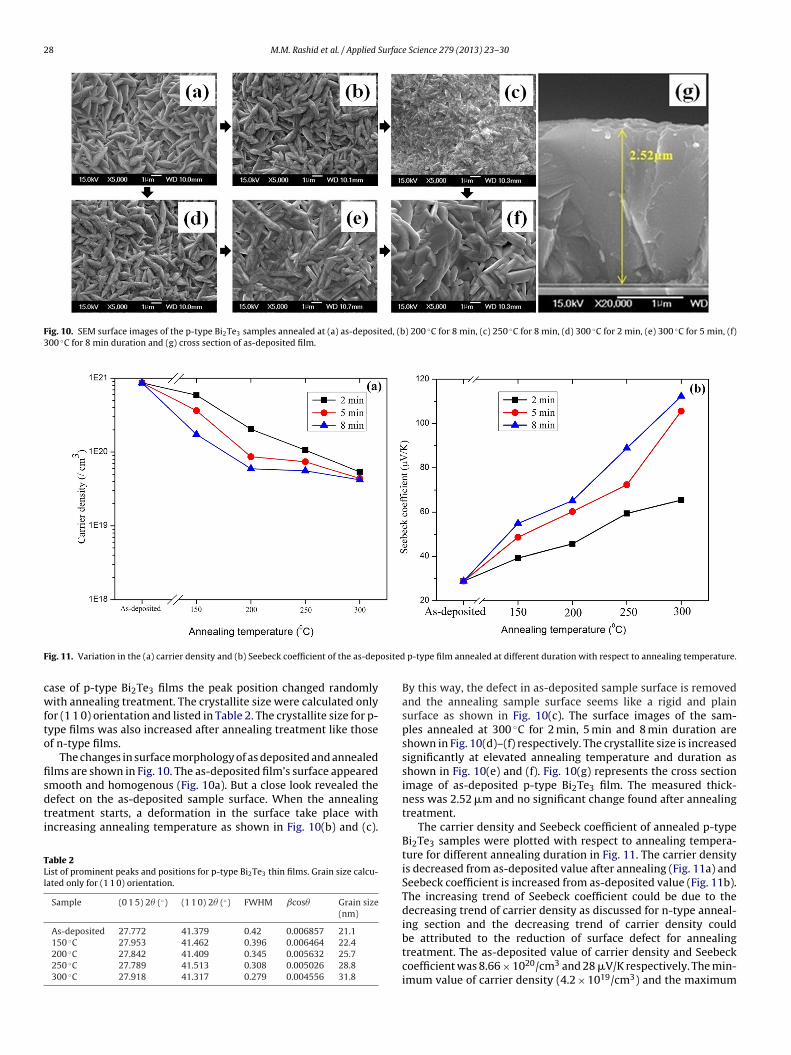
Fig. 10. SEM surface images of the p-type Bi2Te3 samples annealed at (a) as-deposited, (b) 200 ◦C for 8 min, (c) 250 ◦C for 8 min, (d) 300 ◦C for 2 min, (e) 300 ◦C for 5 min, (f)300 ◦C for 8 min duration and (g) cross section of as-deposited film.
F osited
cwfto
fisdti
TLl
ig. 11. Variation in the (a) carrier density and (b) Seebeck coefficient of the as-dep
ase of p-type Bi2Te3 films the peak position changed randomlyith annealing treatment. The crystallite size were calculated only
or (1 1 0) orientation and listed in Table 2. The crystallite size for p-ype films was also increased after annealing treatment like thosef n-type films.
The changes in surface morphology of as deposited and annealedlms are shown in Fig. 10. The as-deposited film’s surface appeared
mooth and homogenous (Fig. 10a). But a close look revealed theefect on the as-deposited sample surface. When the annealingreatment starts, a deformation in the surface take place withncreasing annealing temperature as shown in Fig. 10(b) and (c).able 2ist of prominent peaks and positions for p-type Bi2Te3 thin films. Grain size calcu-ated only for (1 1 0) orientation.
Sample (0 1 5) 2� (◦) (1 1 0) 2� (◦) FWHM ˇcos� Grain size(nm)
As-deposited 27.772 41.379 0.42 0.006857 21.1150 ◦C 27.953 41.462 0.396 0.006464 22.4200 ◦C 27.842 41.409 0.345 0.005632 25.7250 ◦C 27.789 41.513 0.308 0.005026 28.8300 ◦C 27.918 41.317 0.279 0.004556 31.8
p-type film annealed at different duration with respect to annealing temperature.
By this way, the defect in as-deposited sample surface is removedand the annealing sample surface seems like a rigid and plainsurface as shown in Fig. 10(c). The surface images of the sam-ples annealed at 300 ◦C for 2 min, 5 min and 8 min duration areshown in Fig. 10(d)–(f) respectively. The crystallite size is increasedsignificantly at elevated annealing temperature and duration asshown in Fig. 10(e) and (f). Fig. 10(g) represents the cross sectionimage of as-deposited p-type Bi2Te3 film. The measured thick-ness was 2.52 �m and no significant change found after annealingtreatment.
The carrier density and Seebeck coefficient of annealed p-typeBi2Te3 samples were plotted with respect to annealing tempera-ture for different annealing duration in Fig. 11. The carrier densityis decreased from as-deposited value after annealing (Fig. 11a) andSeebeck coefficient is increased from as-deposited value (Fig. 11b).The increasing trend of Seebeck coefficient could be due to thedecreasing trend of carrier density as discussed for n-type anneal-ing section and the decreasing trend of carrier density could
be attributed to the reduction of surface defect for annealingtreatment. The as-deposited value of carrier density and Seebeckcoefficient was 8.66 × 10²⁰/cm3 and 28 �V/K respectively. The min-imum value of carrier density (4.2 × 10¹⁹/cm3) and the maximum
M.M. Rashid et al. / Applied Surface Science 279 (2013) 23– 30 29
F d p-ty
vp
fidi2ipiFt
bcTatta
4
stSemmfram3tfitf8tp
[
[
[
[
[
[
ig. 12. Variation in the (a) carrier mobility and (b) power factor of the as-deposite
alue of Seebeck coefficient (112.3 �V/K) was achieved for the sam-le annealed at 300 ◦C for 8 min duration.
The carrier mobility and power factor of annealed p-type Bi2Te3lms with respect to annealing temperature for different annealinguration plotted in Fig. 12. The carrier mobility increase signif-
cantly from as-deposited value after annealing treatment (from2.32 to 52.312 cm2/V s) and the maximum value of carrier mobil-
ty achieved at 300 ◦C annealing for 8 min duration (Fig. 12a). Theower factor of annealed films is a calculated value, so the change
n power factor with annealing condition is random as shown inig. 12(b). The power factor improved around two-folds (from 2.57o 4.43 �W/K2 cm) from the as-deposited value.
These improvements in Seebeck coefficient and power factor foroth n and p-type Bi2Te3 films was achieved with a very short pro-ess time compared to that of the conventional annealing process.he temperature increment rate, the annealing chamber pressurend the annealing environment, all play a vital role in the rapidhermal annealing process. Therefore, for further optimizing thehermoelectric properties of the Bi2Te3 thin film we will studybout these factors in future.
. Conclusion
In this report, the effects of rapid thermal annealing on thetructural and thermoelectric properties of galvanostatic elec-rodeposited Bi2Te3 films were investigated for the first time.EM imaging and thermoelectric measurements showed that thenhancement of thermoelectric properties could be attributed toicrostructural changes due to the rapid thermal annealing treat-ent. For n-type Bi2Te3 films the Seebeck coefficient and the power
actor of the as-deposited film were improved three- and six-fold,espectively. The maximum Seebeck value (−169.49 �V/K) waschieved by annealing at 300 ◦C for 2 min duration and the maxi-um power factor (17.37 �W/K2 cm) was achieved by annealing at
00 ◦C for 8 min duration. On the other hand, for p-type Bi2Te3 filmshe Seebeck coefficient and the power factor of the as-depositedlm were improved three and two-fold respectively after annealingreatment. The maximum Seebeck value (112.3 �V/K) and power
actor value (4.43 �W/K2 cm) was achieved at 300 ◦C annealing formin duration. The rapid thermal annealing process thus appearso be advantageous in terms of enhancement of the thermoelectricroperties of thermoelectric materials within a short process time.
[
pe film annealed at different duration with respect to annealing temperature.
Acknowledgement
This work was supported by the Excellence program in Schoolof Electrical Engineering at the University of Ulsan.
References
[1] D.M. Rowe, CRC Handbook of Thermoelectric, CRC press, Boca Raton, FL, 1995.[2] S. Udina, M. Carmona, A. Pardo, C. Calaza, J. Santander, L. Fonseca, S. Marco,
A micromachined thermoelectric sensor for natural gas analysis: multivariatecalibration results, Sensors and Actuators B 166 (2012) 338–348.
[3] H.J. Goldsmith, Thermoelectric Refrigeration, Plenum, New York, 1964.[4] H.J. Lee, H.S. Park, S. Han, J.Y. Kim, Thermoelectric properties of n-type Bi-
Te thin films with deposition conditions using RF magnetron co-sputtering,Thermochimica Acta 542 (2012) 57–61.
[5] L.M. Gonclaves, C. Couto, P. Alpuim, A.G. Rolo, F. Volkein, J.H. Correia, Optimiza-tion of thermoelectric properties on Bi2Te3 thin films deposited by thermalco-evporation, Thin Solid Films 518 (2010) 2816–2821.
[6] H. You, S.H. Baek, K.C. Kim, O.J. Kwon, J.S. Kim, C. Park, Growth and thermoelec-tric properties of Bi2Te3 films deposited by modified MOCVD, J. Cryst. Growth346 (2012) 17–21.
[7] N. Peranio, M. Winkler, D. Bessas, Z. Aabdin, J. Konig, H. Bottner, R.P. Her-mann, O. Eibl, Room-temperature MBE deposition, thermoelectric properties,and advanced structural characterization of binary Bi2Te3 and Sb2Te3 thin films,Journal of Alloys and Compounds 521 (2012) 163–173.
[8] Z. Yu, X. Wang, Y. Du, S.A. Yamni, C. Zhang, K. Chuang, S. Li, Fabrication andcharacterization of textured Bi2Te3 thermoelectric thin films prepared on glasssubstrate at room temperature using pulsed laser deposition, J. Cryst. Growth362 (2013) 247–251.
[9] D. Pinisetty, D. Davis, E.J.P. Murphy, M.C. Murphy, A.B. Karki, D.P. Young, R.V.Devireddy, Characterization of electrodeposited bismuth-tellurium nanowiresand nanotubes, Acta Materialia 59 (2011) 2455–2461.
10] Z.G. Zou, K.F. Cai, S. Chen, Z. Qin, Pulsed electrodeposition and characterizationof Bi2Te3-ySey films, Materials Research Bulletin 47 (2012) 3292–3295.
11] F.-H. Li, F.-L. Jia, W. Wang, Studies of electrochemical reduction processesof Bi3+, HTeO2
+ and their mixtures, Applied Surface Science 255 (2009)7394–7402.
12] H.P. Nguyen, M. Wu, J. Su, R.J.M. Vullers, P.M. Vereecken, J. Fransaer, Elec-trodeposition of bismuth telluride thermoelectric thin films from a nonaqueouselectrolyte using ethylene glycol, Electrochim. Acta 68 (2012) 9–17.
13] Y. Ma, A. Jahansson, E. Ahlberg, A.E.C. Palmqvist, A mechanistic study of elec-trodeposition of bismuth telluride on stainless steel substrates, Electrochim.Acta 55 (2010) 4610–4617.
14] S.H. Li, H.M.A. Soliman, J. Zhou, M.S. Toprak, M. Muhammed, D. Platzek, P.Ziolkowski, E. Muller, Effects of annealing and doping on nanostructured bis-muth telluride thick films, Chemistry of Materials 20 (2008) 4403–4410.
15] S.J. Jeon, M. Oh, H. Jeon, S. Hyun, H.J. Lee, Effects of post annealing on thermo-
electric properties of bismuth-tellurium thin films deposited by co-sputtering,Microelectronic Engineering 88 (2011) 541–544.16] L.D. Zhao, B.P. Zhang, W.S. Liu, H.L. Zhang, J.F. Li, Effects of annealing on electricalproperties of n-type Bi2Te3 fabricated by mechanical alloying and spark plasmasintering, Journal of Alloys and Compounds 467 (2009) 91–97.

3 Surfac
[
[
[
[
[[
[
0 M.M. Rashid et al. / Applied
17] B.Y. Yoo, C.-K. Huang, J.R. Lim, J. Herman, M.A. Ryan, J.-P. Fleurial, N.V. Myung,Electrochemically deposited thermoelectric n-type Bi2Te3 thin films, Elec-trochim. Acta 50 (2005) 4371–4377.
18] N.G. Stoltz, G.J. Synder, Effects of annealing electrodeposited bismuth telluridefilms, in: Proceedings of Twenty-First International Conference on Thermo-electrics, 2002, pp. 28–30.
19] B.D. Cullity, Elements of X-ray diffraction, 2nd edition, Addison-Wesley, Read-ing, MA, 1978.
20] D.B. Hyun, J.S. Hwang, J.D. Shim, Thermoelectric properties of (Bi0.25Sb0.75)2Te3
alloys fabricated by hot pressing method, Journal of Materials Science 36 (2001)1285–1291.
[
e Science 279 (2013) 23– 30
21] S.O. Kasap, Principles of Electronic Materials, Mcgraw-Hill, 2005, pp. 167–171.22] H. Huang, W.-L. Luan, S.-T Tu, Influence of annealing on thermoelectric proper-
ties of bismuth telluride films grown via radio frequency magnetron sputtering,Thin Solid Films 517 (2009) 3731–3734.
23] X. Duan, Y. Jiang, Annealing effects on the structural and electrical transportproperties of n-type Bi2Te2.7Se0.3 thin films deposited by flash evaporation,
Applied Surface Science 256 (2010) 7365–7370.24] Z.-H. Zheng, P. Fan, G.-X. Liang, D.-P. Zhang, X.-M. Cai, T.-B. Chen, Anneal-ing temperature influence on electrical properties of ion beam sputteredBi2Te3 thin films, Journal of Physics and Chemistry of Solids 71 (2010)1713–1716.
Related Documents