Simulation of Full Duplex Communication Systems April 24, 2019 Radha Krishna Ganti [email protected] Joint work with Aniruddhan, Abhishek, Arjun Nadh

Welcome message from author
This document is posted to help you gain knowledge. Please leave a comment to let me know what you think about it! Share it to your friends and learn new things together.
Transcript

Simulation of Full Duplex Communication Systems
April 24, 2019Radha Krishna [email protected]
Joint work with Aniruddhan, Abhishek, Arjun Nadh
Current wireless devices are half-duplex
Time
Freq
uenc
y
TimeFr
eque
ncy
Half-duplex
Time
Freq
uenc
y
Full-duplex
Ideal full-duplex doubles the available resources

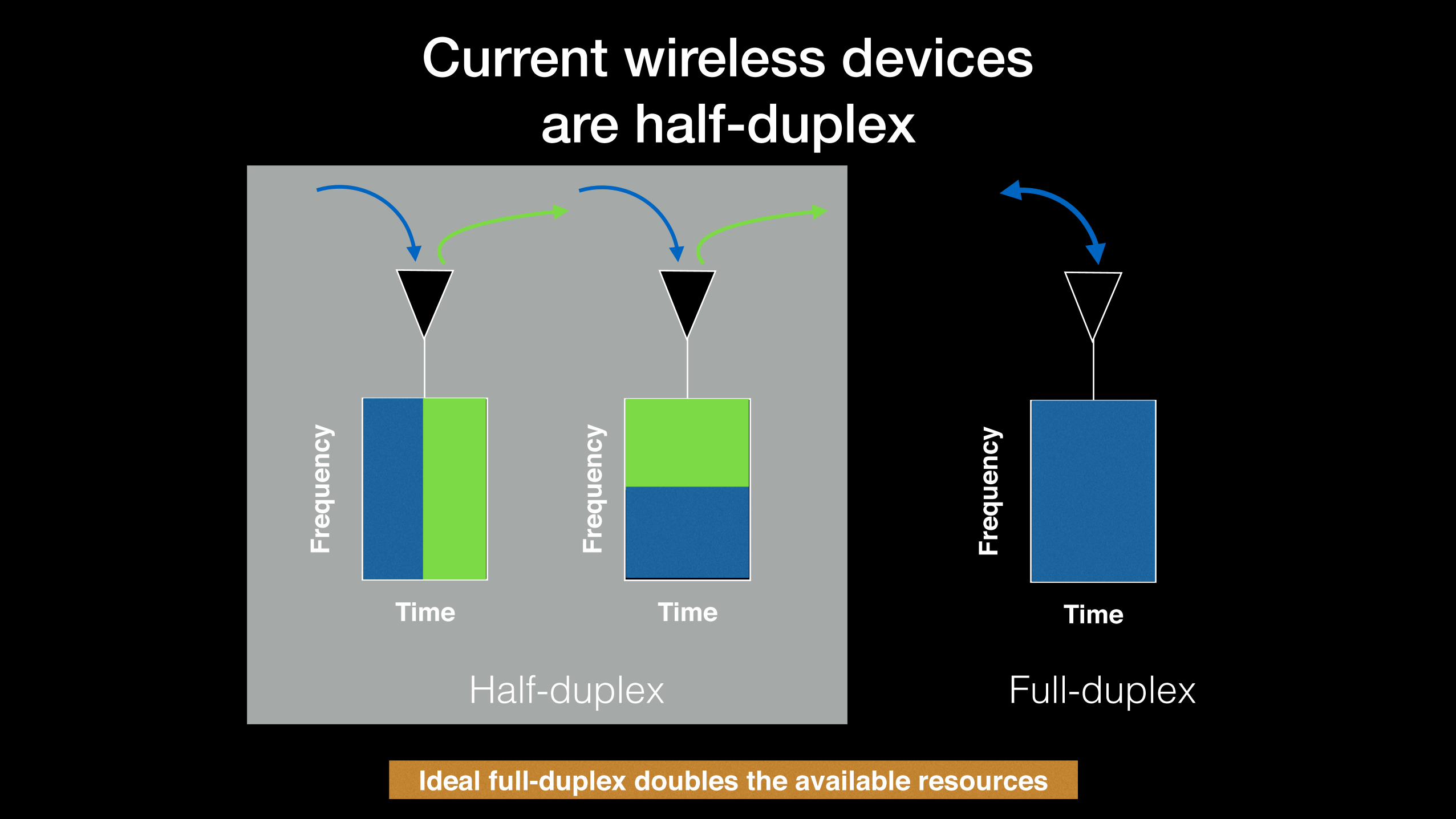
Why is it difficult?
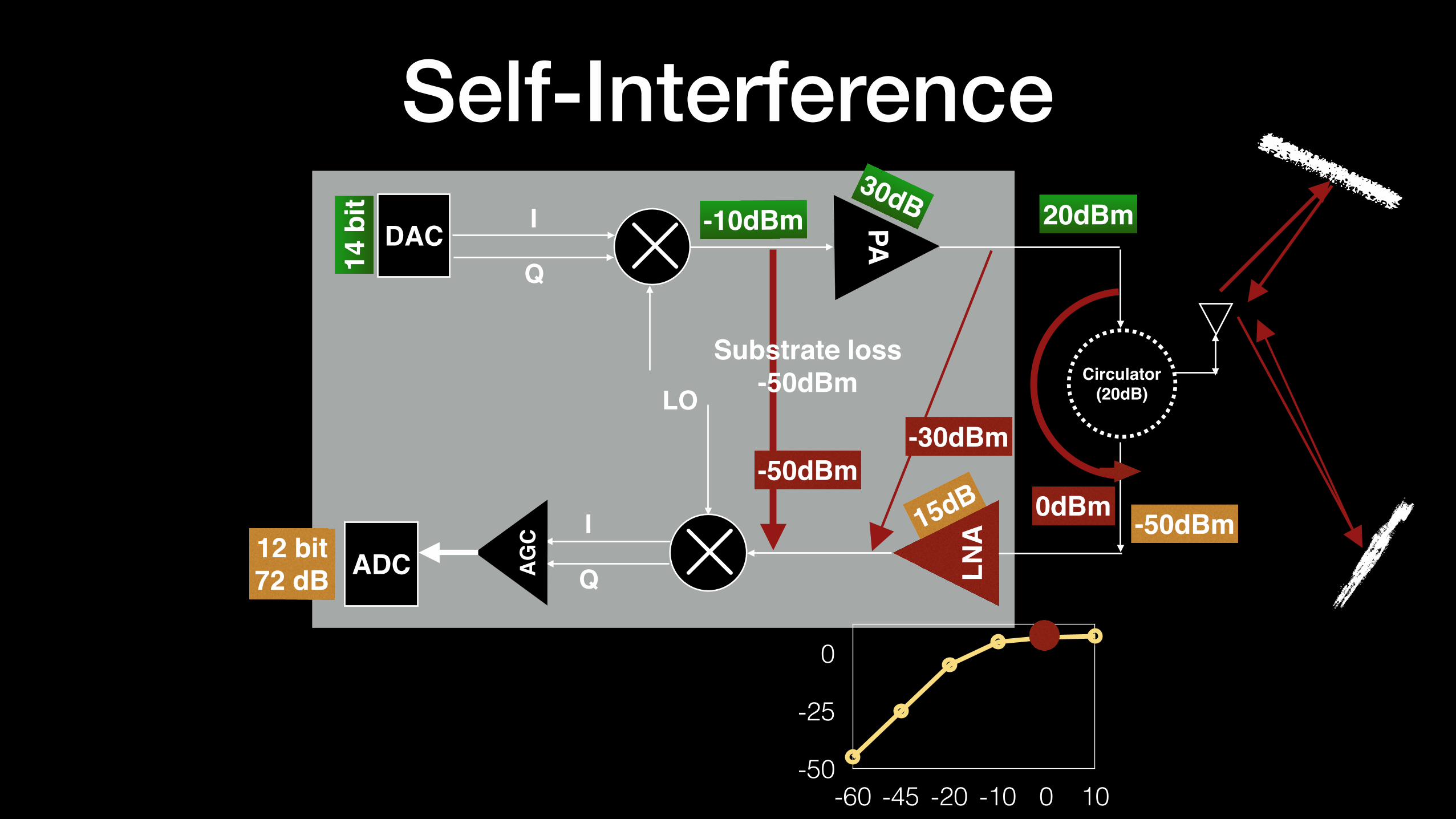
Self interference
Transmit signal: 20dBm
Receive signal: -70dB,
Transmit signal is about a billion times
stronger than the receive signal
Large dynamic range
Typical TX-RX numbersDAC
PAI
Q
Mixer
⇥30dB-10dBm 20dBm
14 b
it
-50
-25
0
-60 -45 -20 -10 0 10
-50dBm
ADC LNAI
QMixer
AG
C
12 bit72 dB
15dB
⇥ -35dBm
Duplexer(50dB)
Freq: f2
Freq: f1
LO
e�j2⇡f2t+�r(t)
e�j2⇡f1t+�T (t)
Self-InterferenceDAC PAI
Q
30dB-10dBm
14 b
it
ADC LNAI
Q
LO
AG
C12 bit72 dB
Circulator (20dB)
20dBm
-50
-25
0
-60 -45 -20 -10 0 10
0dBm -50dBm
Substrate loss-50dBm
-50dBm-30dBm
15dB
⇥
⇥
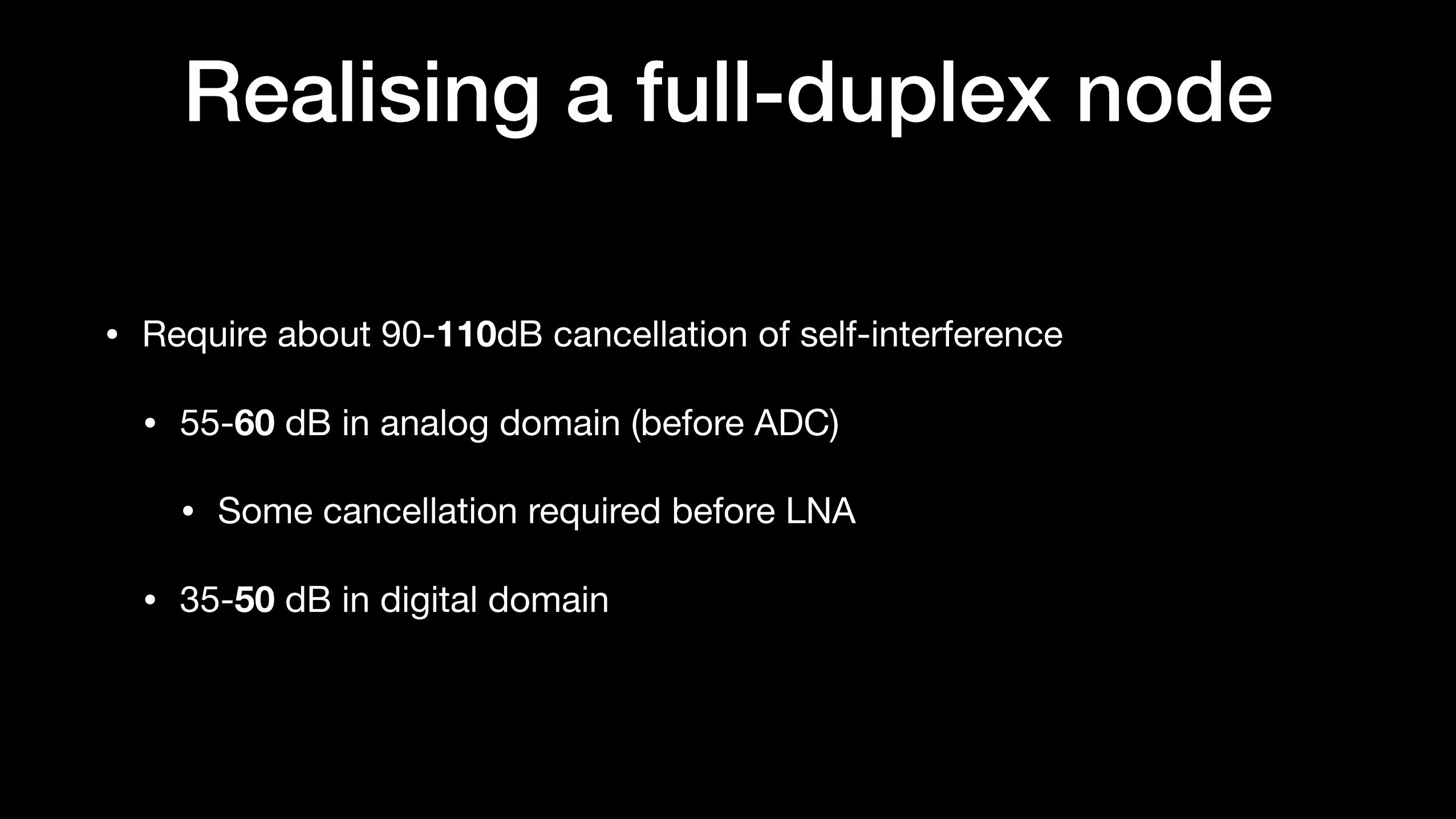
Realising a full-duplex node
• Require about 90-110dB cancellation of self-interference
• 55-60 dB in analog domain (before ADC)
• Some cancellation required before LNA
• 35-50 dB in digital domain
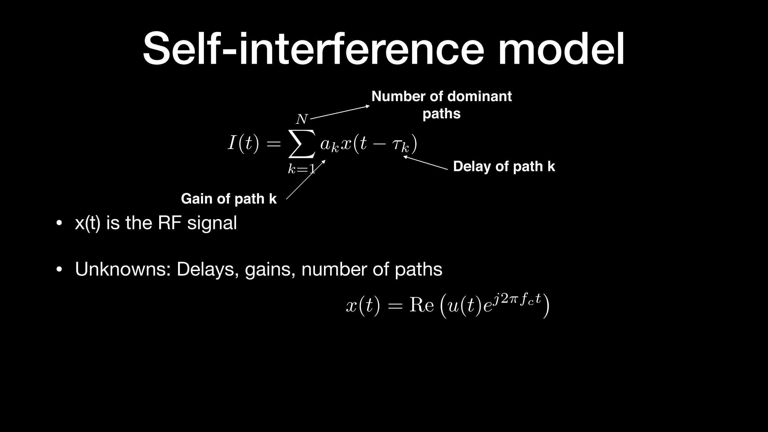
Self-interference model
I(t) =NX
k=1
akx(t� ⌧k)
Gain of path k
Delay of path k
Number of dominantpaths
• x(t) is the RF signal
• Unknowns: Delays, gains, number of paths
x(t) = Re�u(t)ej2⇡fct
�
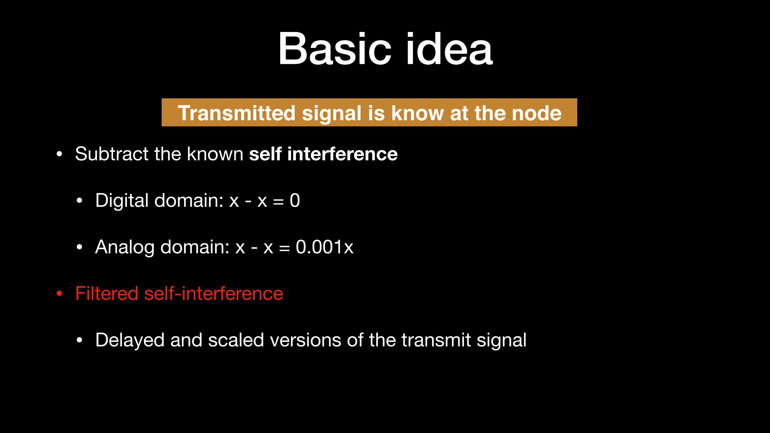
Basic idea
• Subtract the known self interference
• Digital domain: x - x = 0
• Analog domain: x - x = 0.001x
• Filtered self-interference
• Delayed and scaled versions of the transmit signal
Transmitted signal is know at the node
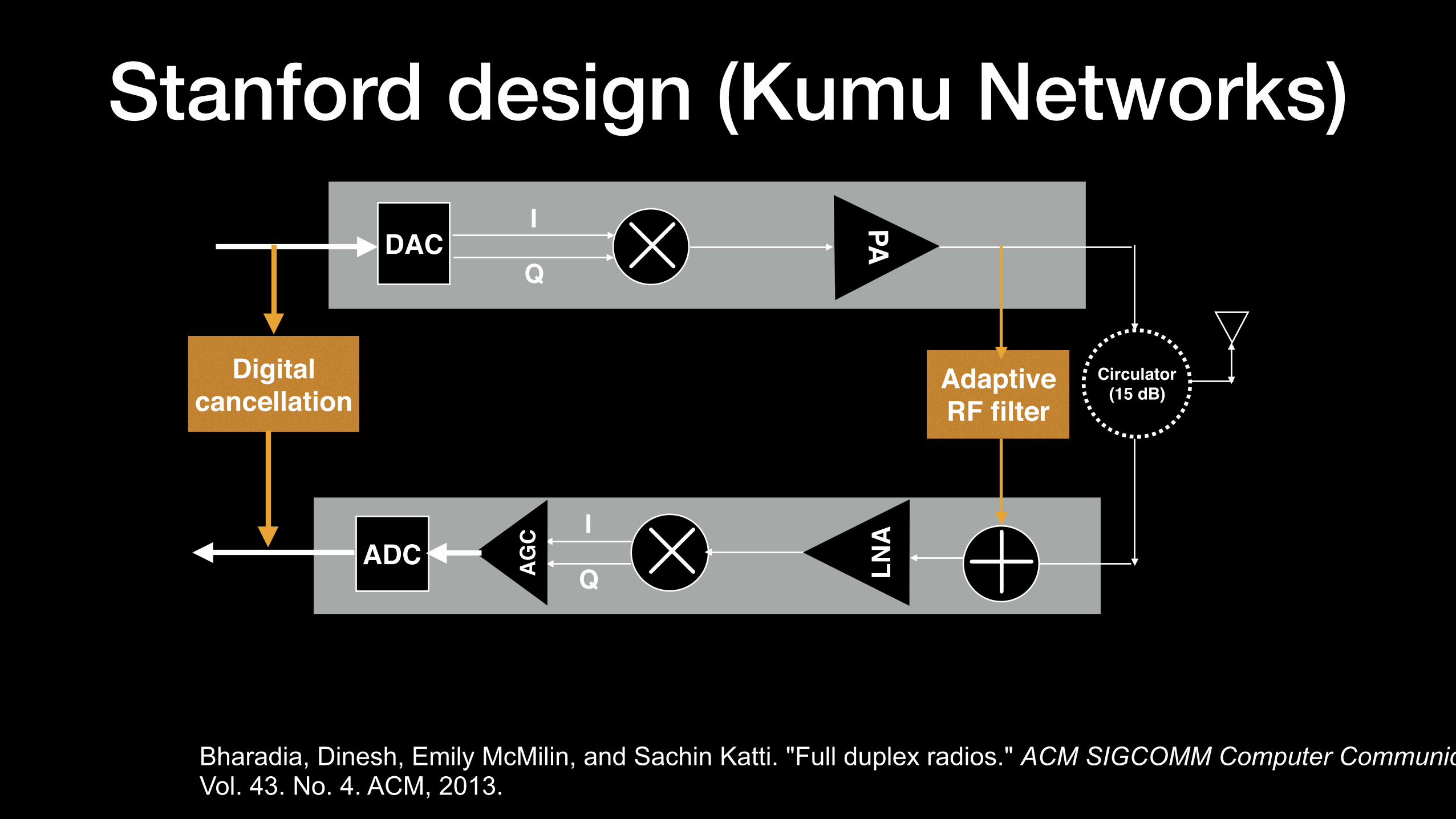
Stanford design (Kumu Networks)DAC
PAI
Q
ADC LNAI
QAG
C
Circulator (15 dB)Adaptive
RF filterDigital
cancellation
Bharadia, Dinesh, Emily McMilin, and Sachin Katti. "Full duplex radios." ACM SIGCOMM Computer Communication Review. Vol. 43. No. 4. ACM, 2013.
⇥
⇥ +
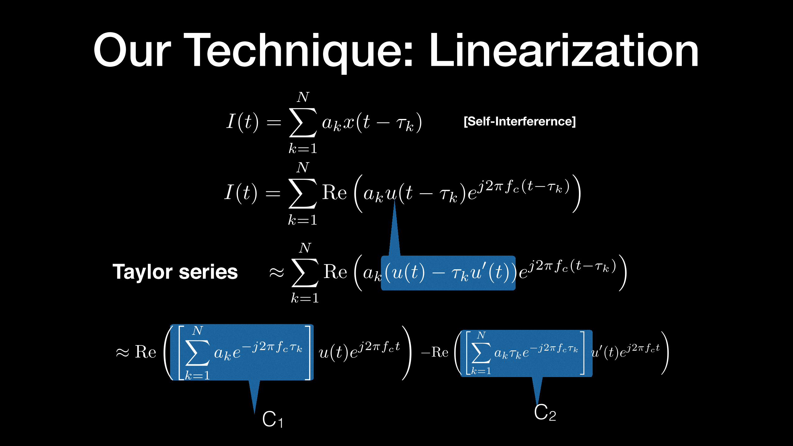
Our Technique: Linearization
I(t) =NX
k=1
Re⇣aku(t� ⌧k)e
j2⇡fc(t�⌧k)⌘
⇡NX
k=1
Re⇣ak(u(t)� ⌧ku
0(t))ej2⇡fc(t�⌧k)⌘
⇡ Re
"NX
k=1
ake�j2⇡fc⌧k
#u(t)ej2⇡fct
!�Re
"NX
k=1
ak⌧ke�j2⇡fc⌧k
#u0(t)ej2⇡fct
!
Taylor series
C1 C2
I(t) =NX
k=1
akx(t� ⌧k) [Self-Interferernce]
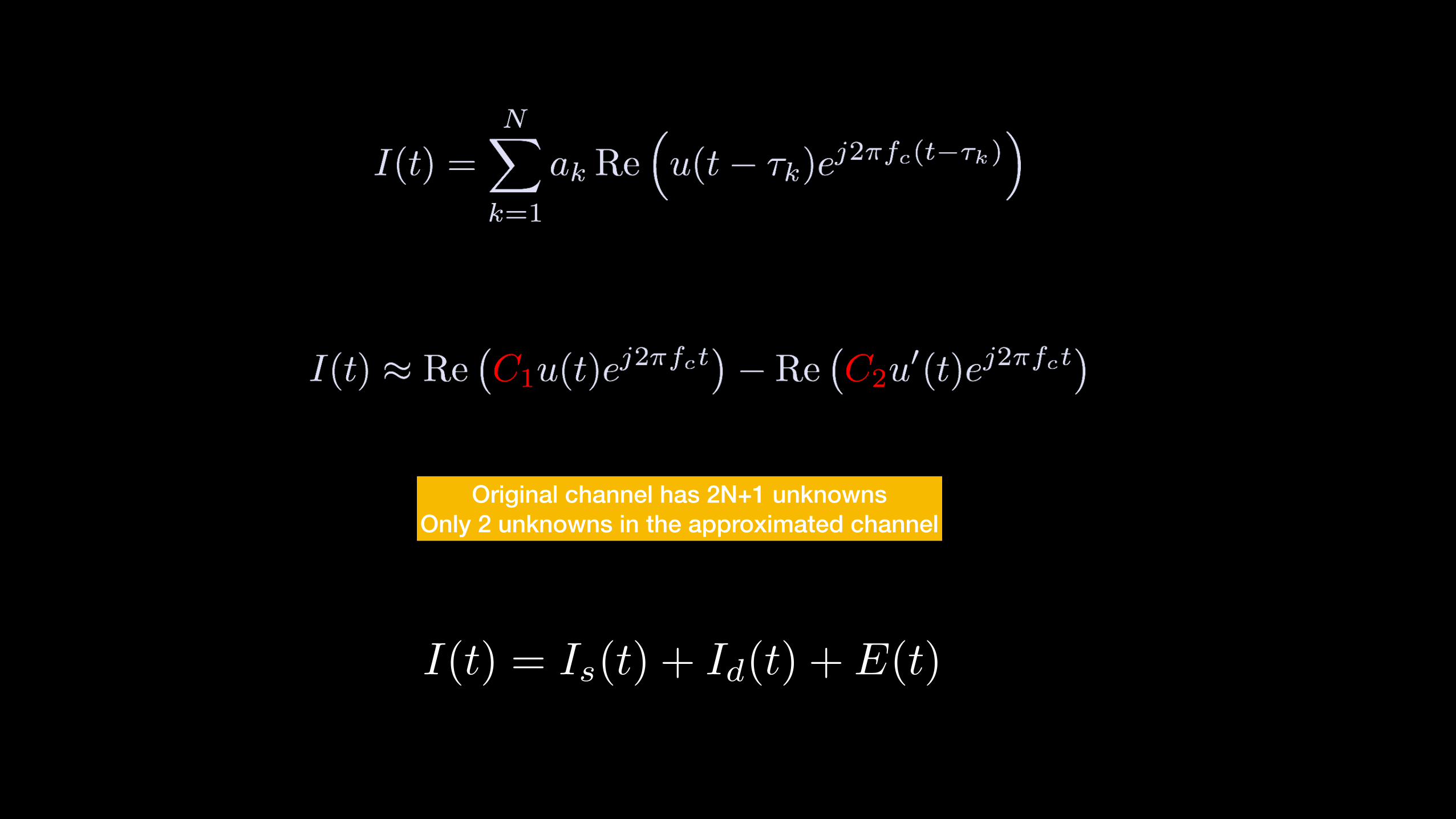
I(t) = Is(t) + Id(t) + E(t)
Original channel has 2N+1 unknowns Only 2 unknowns in the approximated channel
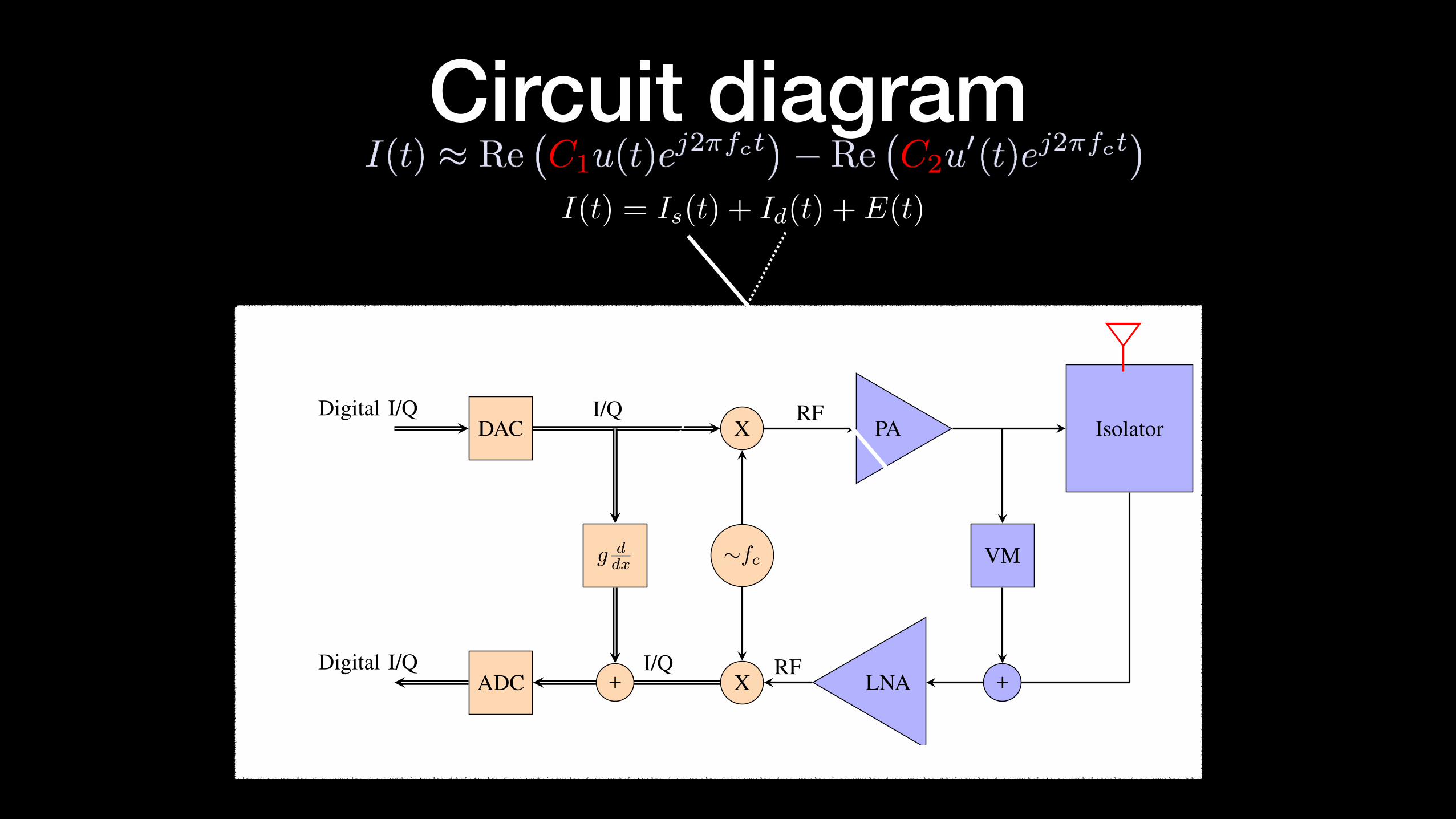
Circuit diagram
DACDigital I/Q
XI/Q
PARF
Isolator
VMg ddx ⇠fc
ADCDigital I/Q
XI/Q
LNARF ++
Fig. 3: Canceling Id(t) in the analog domain. The derivative canceler is implemented in the analog domain after down conversionand before the ADC. This block is represented as g d
dx , where g represents the tunable complex gain of the IQ paths.
Where E(t) is the down converted error signal E(t). It canbe easily shown thatZ ⌫
�⌫x(t)x0(t)dt =
Z ⌫
�⌫E(t)x0(t)dt =
Z ⌫
�⌫x(t)E(t)dt = 0.
Hence the error simplifies to
�(�1,�2) = |C1 � �1|2px + |�2 � C2|2p0x + pE ,
where px is the power in x(t) and p0x is the power inthe derivative signal. The above error expression also showsthat the optimization over the signal and its derivative canbe done jointly or individually. Depending on the particularoptimization, various circuits for cancellation can be realized.
A. Cancellation of the signal term
The signal term Is(t) can be rewritten as
Is(t) = Re[|C1|x(t)ej2⇡fct+j arg(C1)],
where |C1| represents the absolute value of C1 and arg denotesthe angle (argument) of the complex number. So Is(t) can beobtained by scaling the transmitted RF signal y(t) by |C1|and phase-shifting the carrier by arg(C1). The scaling canbe achieved by an RF attenuator. The phase change can beobtained by a vector modulator (or a RF phase shifter). SeeFigure 4. A vector modulator just changes the phase of thecarrier and the gain of the signal. So the output of a vectormodulator with x(t) as the input can be modeled as
Z(t) = �Re[x(t)ej2⇡fct+j✓],
where the ✓ and the gain (or attenuation) � can be appropri-ately controlled, based on the range and the resolution of thevector modulator. A simple gradient descent algorithm basedon the error vector magnitude can be used to control the gainG and the phase ✓. In Figure 5, the spectrum of I(t)� Id(t)is plotted. We observe a frequency dependent residual signal,indicating the presence of x0(t).
0/90o
Gain2
Gain1
+Re(x(t)ej2⇡fct) GRe(x(t)ej2⇡fct+j✓)
Fig. 4: Illustration of a RF vector modulator that can be usedfor phase shifting a signal.
B. Cancellation of the derivative term
The derivative term can be canceled in the RF domain oranalog domain (after down conversion) or the digital domain.
1) Analog domain cancellation: A differetiator can beeasily implemented in the analog domain using a resistor inseries with a capacitor across a large gain amplifier. See Figure3. The real part and the imaginary part (I and Q) have tobe scaled jointly so as to achieve the optimal cancellation.Alternatively, the cancellation of the signal x(t) can also beachieved at the analog domain after the down conversion.
2) Digital domain cancellation: A digital domain differen-tiator can be realized by any filter with response j! in thefrequency domain. However, this filter cannot be realized ifthe sampling rate is equal to the Nyquist rate of the signal.However, a good approximation of the derivative can beobtained if the signal is over sampled. See Figure 6.
C. Advantages of analog domain cancellation
1) Canceling more self-interference before the analog todigital converter would increase the bit resolution of thereceived signal, thereby improving the effective receivedSNR.
2) Digital cancellation would require realizing the filter j!,which cannot be realized when the sampling rate is equal
I(t) = Is(t) + Id(t) + E(t)
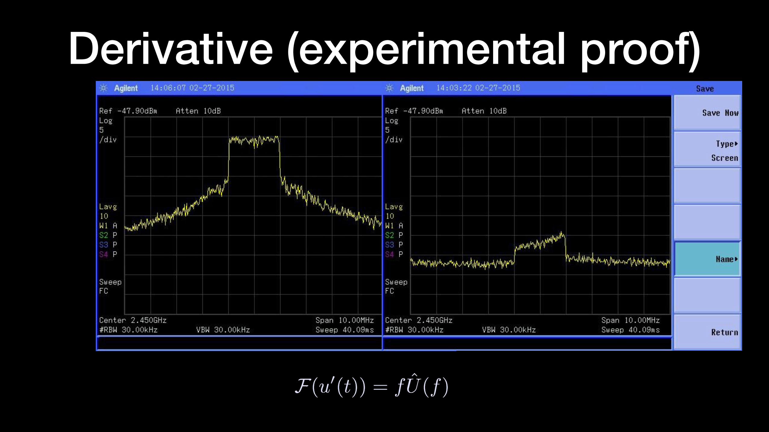
Derivative (experimental proof)
10
-10 -5 0 5 10
Transmit power (dBm)
30
35
40
45
50
55
60
65
70
75
80
Cance
llatio
n (
dB
)
Cancellation versus transmit power for 20 MHz OFDM
Total cancellation
Analog cancellation
Digital cancellation
Fig. 12: Analog and digital cancellation versus transmit powerfor a 20 MHz OFDM signal with antenna.
till about 5 dBm input power after which it reduces. Thisis mainly because of the power amplifier non-linearities. As
-10 -5 0 5 10
Transmit power (dBm)
15
20
25
30
35
40
Cance
llatio
n (
dB
)
Cancellation versus transmit power for 20 MHz OFDM
1st derivative
1st derivative + 2nd derivative
Total digital cancellation
Fig. 13: Split-up of the digital cancellation versus transmitpower for a 20 MHz OFDM signal with antenna.
mentioned earlier, the digital cancellation consists of removingthe signal, the derivative and the second order derivative com-ponents. In Figure 13, this split-up is provided as a function ofthe transmit power. We see that the first-derivative cancellationprovides the maximum cancellation. However, the second-derivative also gives about 5-6 dB of cancellation. The self-interference after analog cancellation is I(t) = Is(t) + Id(t),i.e., a sum of the the signal and the derivative terms. Thissignal is received in the digital domain after sampling by theADC. Since the initial phase of the sampling time cannot becontrolled, the received self-interference in the digital domainis I(nT + �) = Is(nT + �)+ Id(nT + �), n = 1, 2, . . ., whereT is the sampling duration and 0 � T . However we
only have access to the transmitted signal x(nT ). Since � issmall, Is(nT + �) = a0x(nT + �) can be approximated (afterappropriate scaling by a0) by x(nT ) and x
0(nT ). SimilarlyId(nT + �) = c1x
0(nT + �) can be approximated by x0(nT )
and the second derivative x00(nT ). Hence using the second
derivative improves the overall cancellation.
Transmit power (dBm)-5 0 5 10 15 20
Cance
llatio
n (
dB
)
20
30
40
50
60
70
80Cancellation versus transmit power for 10 MHz SC
Total cancellationAnalog cancellationDigital cancellation
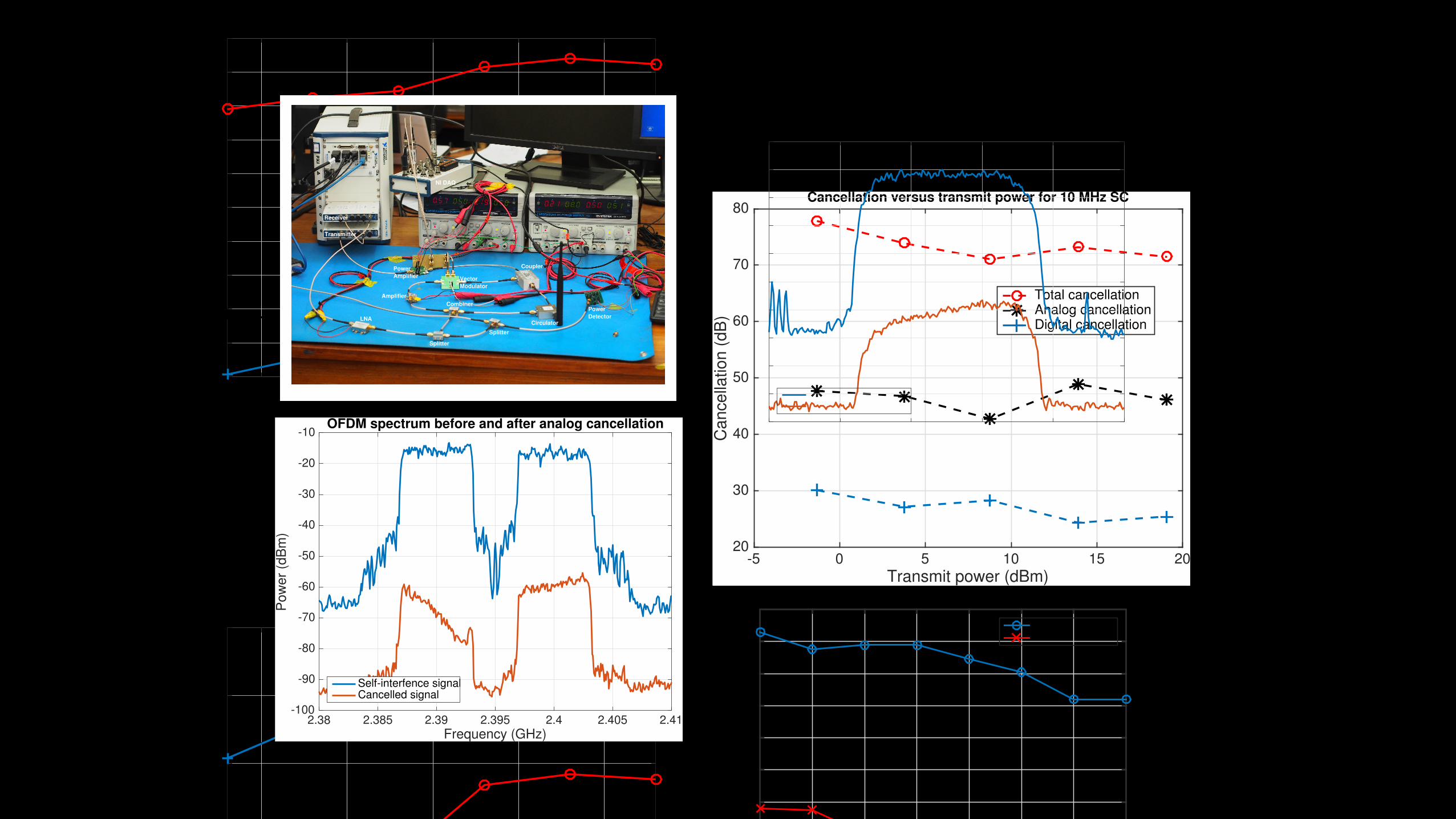
Fig. 14: Cancellation vs Transmit power for different band-widths with single carrier as transmit waveform. These resultswere obtained with port 2 of the circulator connected to anantenna.
For a single carrier transmission, the cancellation is plottedas a function of the transmitted power in Fig. 14. Overall, weobserve about 75 dBm cancellation for both OFDM and single-carrier waveforms. Thus the overall cancellation is imperviousto the transmitted waveform.
VI. CONCLUSION
Robust self-interference cancellation is critical to realis-ing full-duplex capable wireless nodes. However a majorimpediment to self-interference cancellation is estimation ofthe multi-path channel through which the transmitted signalreaches the shared antenna. A part of the channel has tobe estimated in the analog (RF) domain, and used for self-interference cancellation before the LNA, while the remainingpart of the channel has to be estimated in either the analogbaseband or in the digital domain. In the current literature, thechannel is modelled as an M -tap delay-line filter and the filtercoefficients are estimated in the RF and digital domain. In allthe works, there was no prior knowledge on M , and hence alarge number of taps are assumed.
In this work, using Talyor series approximation, we reducethe dimensionality of the parameter space to two (or three).In particular, we show that the self-interference can be mod-elled as a linear combination of the original signal and itsderivatives. We propose a new self-interference cancellationarchitecture that utilises the linearized channel model. Theself-interference model, and in particular the presence of thederivative component of the signal is verified by experiments.
9
cancellation to the power of the SI signal before cancellation.The ratio is expressed in dB. Note that the power of the SIsignal before cancellation is the same as transmit power at theantenna port (port 2) of the circulator.
In Figure 9, the spectrum of the self-interference signal isplotted when an OFDM signal is transmitted at 4 dBm (atport 2 of the circulator). In the same figure, the residual self-interference is plotted after analog cancellation. About 54 dBof self-interference was cancelled in the analog domain. Moreimportantly, the linear slope in the residual self-interferencespectrum indicates that the residual signal is dominated bythe derivative component Id(t), thus verifying the derivativeapproximation and in particular (6). In Figure 10, the spectra
2.38 2.385 2.39 2.395 2.4 2.405 2.41Frequency (GHz)
-100
-90
-80
-70
-60
-50
-40
-30
-20
-10
Pow
er
(dB
m)
OFDM spectrum before and after analog cancellation
Self-interfence signalCancelled signal
Fig. 9: The spectrum of the self-interference signal of a 20MHz OFDM transmission. Also, the self-interference spec-trum after analog cancellation is plotted. The transmit power(at the antenna port) is 4 dBm and the analog cancellation isabout 54 dB. The linear slope in the residual self-interferenceindicates a derivative component.
of the self-interference and the cancelled signal (57 dB analogcancellation) are plotted when a single-carrier signal is trans-mitted. As in the OFDM signal, the residual self-interferenceexhibits a large derivative component.
In Figure 11, the analog cancellation6 is plotted as a functionof the signal bandwidth. We observe that the analog cancella-tion decreases with increasing bandwidth. This is because thederivative component in the residual self-interference signalincreases with increasing bandwidth. Since analog cancellationonly removes Is(t), the residual power increases with increas-ing bandwidth, and thus lowering the analog cancellation. Thetop curve in the plot corresponds to the case when the antennaport was terminated by a 50 ⌦ terminator, while the bottomcurve corresponds to measurements with an antenna. In thecase of 50 ⌦ termination, the self-interference multi-path isprimarily through the circulator, while with antenna, therewill be multiple paths due to reflections too. In addition, thecharacteristic impedance of the antenna will not be as close
6The reported analog cancellation also includes the 18 dB isolation of thecirculator.
2.39 2.392 2.394 2.396 2.398 2.4Frequency (GHz)
-100
-90
-80
-70
-60
-50
-40
-30
-20
-10
0
Pow
er
(dB
m)
SC spectrum before and after analog cancellation
Self-interfence signalCancelled signal
Fig. 10: The spectrum of the self-interference and the residualsignal of a 10 MHz 4-QAM single carrier transmission. Thetransmit power (at the antenna port) is 4 dBm and the analogcancellation is about 57 dB. The linear slope in the residualself-interference indicates a derivative component.
Bandwidth MHz10 20 30 40 50 60 70 80
Analo
g c
ance
llatio
n d
B
32
34
36
38
40
42
44
46
48
50Analog cancellation versus BW for an OFDM signal
Without antennaWith antenna
Fig. 11: Analog cancellation versus transmit BW for an OFDMsignal with and without antenna. In the second case (withoutantenna), the antenna port is terminated by a 50 ⌦ terminator.
to 50 ⌦ as a terminator. This impedance mismatch causesRF signals to get reflected back from the antenna (insteadof getting transmitted). Because of these two effects, theaggregate power in the derivative component increases in thecase of antenna. This reduces causes the reduction in analogcancellation.
In Figure 12, the analog and digital cancellation are plottedas a function of the transmit power. We observe that the analogcancellation is almost constant with respect to increasing trans-mit power. This is expected since the analog cancellation doesnot depend on the signal SNR and depends only on the reso-lution of the phase and amplitude of the VM, which are fixed.The digital cancellation is increasing with the transmit power
8
Once a0, c1 and c2 have been obtained, the self-interferencesignal can be reconstructed and subtracted from the receivedsignal.
V. EXPERIMENTAL RESULTS
In this Section, we provide experimental results to validatethe channel model and the derivative based cancellation.We demonstrate the ability of the proposed derivative basedarchitecture to suppress the self-interference signal and weprovide quantitative measure in terms of cancellation for thesame.
A. Experimental setupOur experimental setup is shown in Fig. 8. We use a
National Instruments (NI) PXIe based software defined ra-dio (NI5791) for transmission and reception. The maximumtransmit power possible in NI5791 is 5 dBm and we usean external power amplifier (PA) (Skyworks SE2576L) at thetransmitter. We use a shared antenna architecture wherein thesame antenna is used for transmission and reception. Theisolation between transmit and receive chain is provided bya circulator (Pasternack PE8401). This circulator provides 18dB of isolation between port 1 and port 3. The transmit signalis fed into port 1 and the antenna is connected to port 2. Thesignal from port 3 will therefore contain the received signal aswell as the self-interference signal. Two copies of the transmitsignal from PA are obtained using a directional coupler (Mini-Circuits ZHDC-16-63-S+), wherein one is connected to theinput port of the circulator and the other is used as an inputto the vector modulator (Hittite HMC631LP3). The directionalcoupler allows for tapping a copy of a signal with minimal lossin the mainline, thus the output at the coupled port is muchlower in power3. The VM also introduces an attenuation andthus the power at its output may be insufficient to suppressthe self-interference. The output of VM is passed through anamplifier (Mini-Circuits ZX60-P33ULN+) in order to recoverthis loss in power. The self-interference signal at port 3 of thecirculator is comprised of the transmit signal leaked throughthe circulator and multiple reflected copies of the transmitsignal received by the antenna.
As mentioned earlier, the signal component (Is(t)) of theself-interference is cancelled in the RF domain. The vectormodulator is used to adapt the gain and phase of the tappedtransmitted signal and match it to the Is(t) component ofthe self-interference. The gain and phase of the VM arecontrolled by two DC voltages generated by an NI DataAcquisition Device (DAQ)4. The output of the VM and theself-interference signal (from the receive port of the circulator)are summed by a power combiner (Mini-Circuits ZX10-2-232-S+). A part of this summed signal is fed to a true RMS powerdetector (PD) (Hittite HMC1020LP4ETR) via a power splitterto observe the power in the residual signal. The PD generates
3A lower power at the input of the VM is desirable since the P1 dB ofthe VM that we use is 21 dBm and a lower power at its input prevents anysignificant non-linearity at the output of the VM.
4Consists of 16-bit analog-to-digital converters (ADC) and 16-bit digital-to-analog converters (DAC) controllable by a desktop computer
Vector
Modulator
Coupler
Power
DetectorCirculator
Receiver
LNA
Amplifier
Combiner
Splitter
Splitter
Transmitter
Power
Amplifier
NI DAQ
Fig. 8: Experiment Setup
a DC voltage proportional to the input power. This voltage issampled by the NI DAQ. The optimal DC control voltages ofthe VM are found by an adaptive search that minimizes theresidual self-interference power.
The residual signal after the combiner is fed to the NI5791receiver5. The received samples comprise of the signal termand the derivative term. A part of these samples are trainingsymbols. They are processed offline to obtain a0, c1 andc2. These estimated parameters are then used to reconstructand cancel self-interference for the remaining samples. ((Non-linear cancellation of the third and fifth harmonic is also usedto mitigate the non-linear effects of the PA.))
We obtain the cancellation results for OFDM and single-carrier modulated waveforms.
1) OFDM: We consider an OFDM signal with 1024 sub-carriers of which 620 are useful subcarriers (the rest are nulledout at the DC and at the edge of the band). At the receiver weuse an oversampling factor of 4. The maximum sampling ratethat can be practically achieved using PXIe is 80 MS/s. Hencewith an oversampling factor of 4, the maximum bandwidth ofOFDM signal that can be transmitted is 20 MHz. The P1dBof the PA is 32 dBm. The measured PAPR (Peak to AveragePower Ratio) of the transmitted OFDM waveform was 13 dBand hence the maximum average transmit power was restrictedto 19 dBm to avoid severe non-linearities. The spectrum of a20 MHz OFDM signal that is used is plotted in Figure 9.
2) Single-carrier: A 4-QAM single-carrier signal was alsoused for the experiments. An RRC pulse shaping filter withroll-off factor 0.3 was used. The PAPR of the signal wasmeasured to be 4 dB which is about 9 dB lower than thatof OFDM. Hence, with the same PA, the single carrier can betransmitted at higher power than OFDM without PA saturation.
We use 2.395 GHz as the center frequency for all theexperiments. This was done mainly to avoid interference fromthe ISM band.
B. Results and discussionFollowing the standard convention in literature, we define
cancellation to be ratio of power of the SI signal after
5The minimum RF power at the input of 5791, that induces full-scaleswing at the ADC is -27 dBm. Since the residual self-interference signalis much lower in power, we use an (Mini-Circuits ZX60-242GLN-S+) beforethe NI5791 module, to prevent effect of quantization noise.

Hardware New idea: 6 months (might not work)
RF Blockset to the rescue
Software ??
RF Blockset• OFDM modulation
• RF Blockset: Circuit-envelope blocks to model the RF
• Analog cancellation
• Self-Interference channel model
• Digital cancellation
• Signal and derivative cancellation
Blocks Used• IQ Modulator/ IQ Demodulator
• Variable RF phase shifter
• Variable RF attenuator
• Custom analog cancellation algorithm (gradient descent)
• Level-2 MATLAB S-Function
• Custom digital cancellation algorithm (derivative and LMS)
• Level-2 MATLAB S-Function
Novice user: 1 week
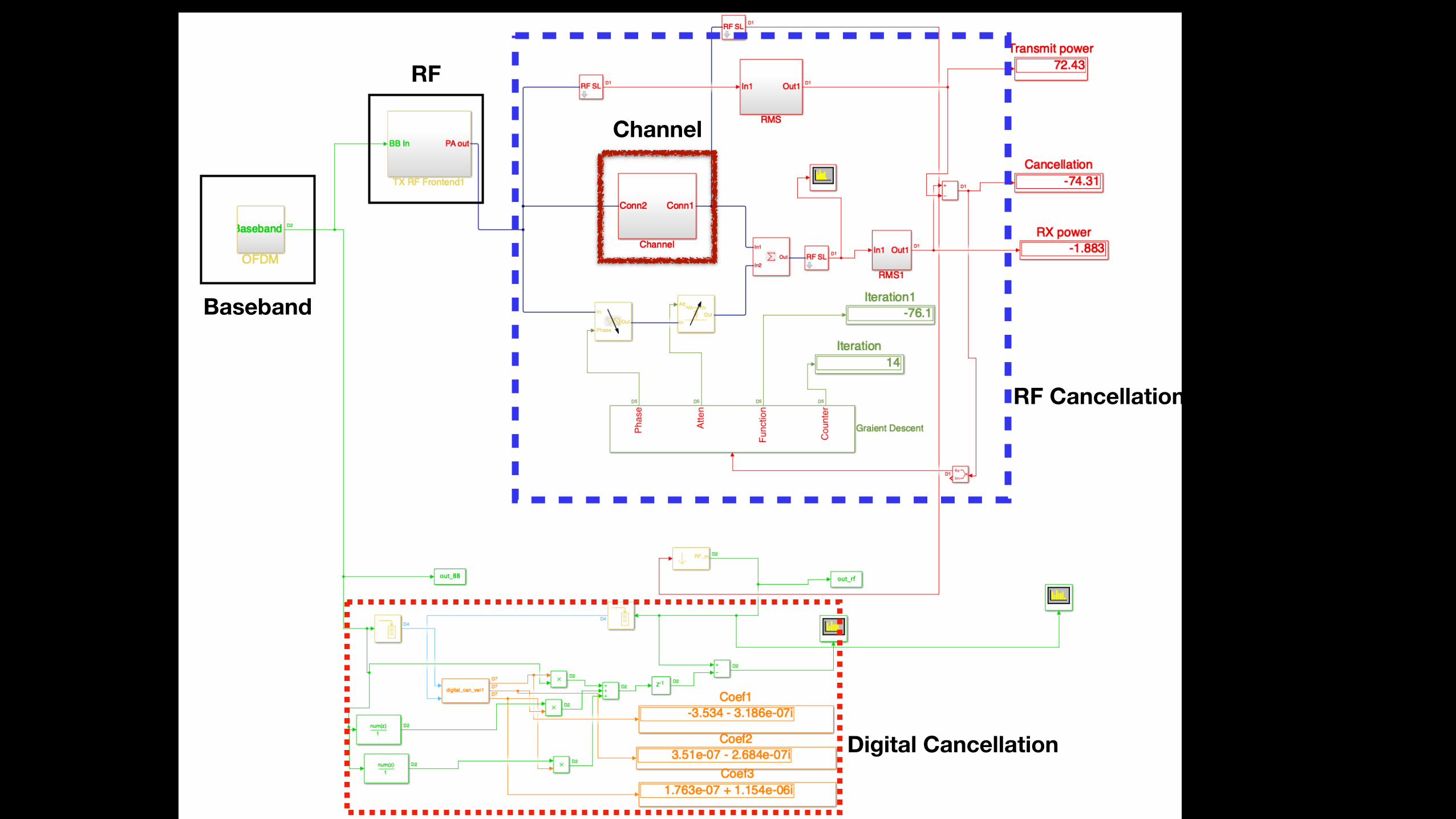
Baseband
RF
RF Cancellation
Digital Cancellation
Channel
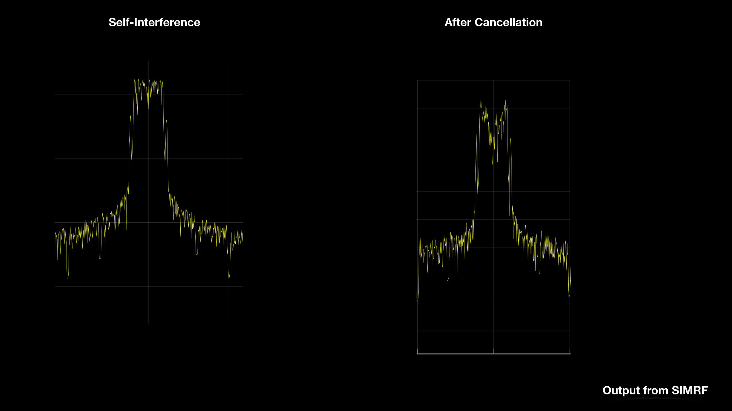
Self-Interference After Cancellation
Output from SIMRF
Learning
Power Amplifier Circulator
Amplitude and
Phase Sum
Power Detector
Antenna
DiffPower Detector
x(t)
r(t)
Gradient descent
Faster GD convergence
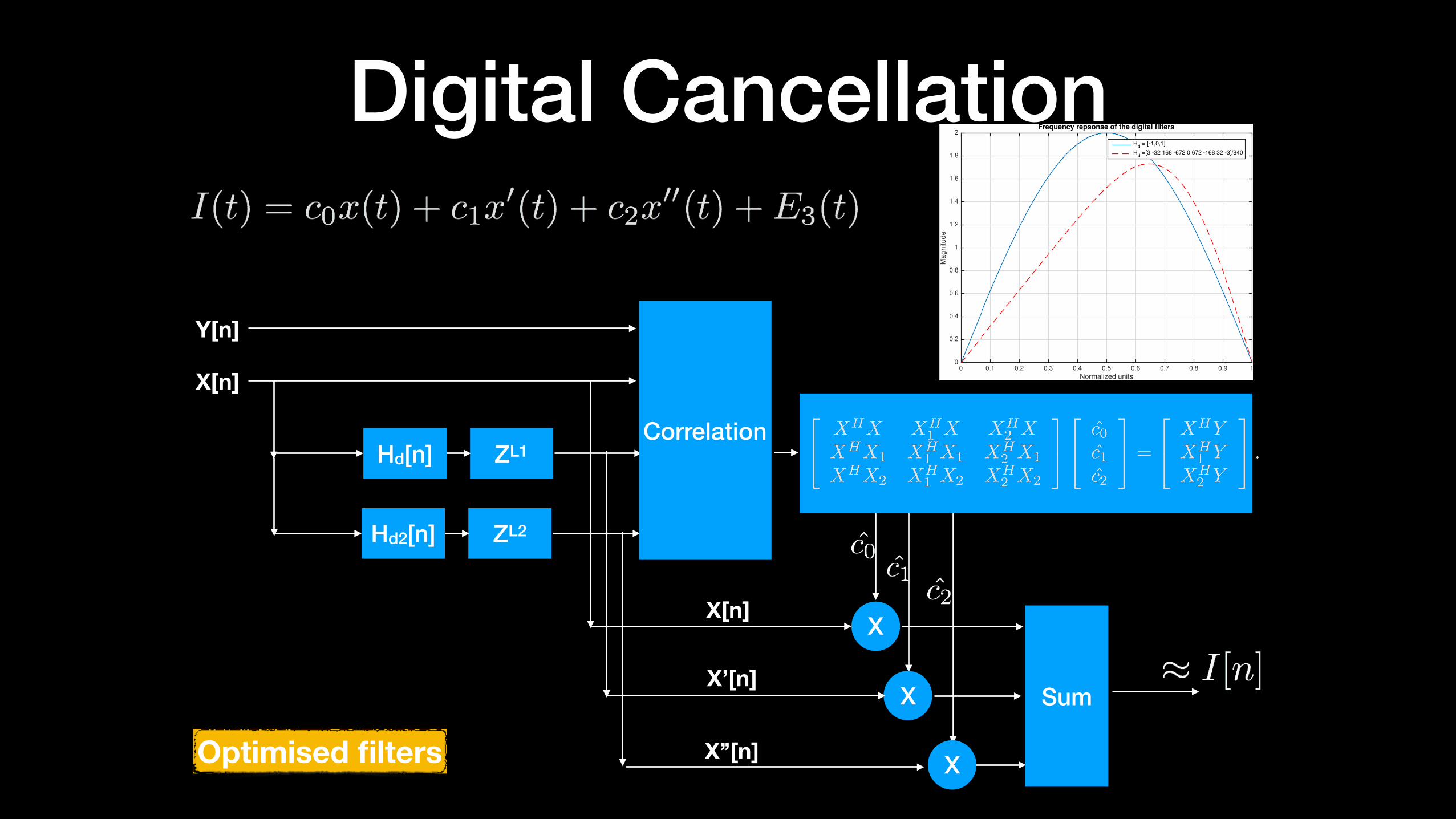
Digital Cancellation 7
received signal, thereby improving the effective receivedsignal-to-noise ratio (SNR).
2) Digital cancellation would require realizing the filter j!,which cannot be realized when the sampling rate is equalto the bandwidth. Realizing an approximate filter wouldrequire oversampling the signal thereby increasing thecomplexity of the ADC.
As shown in Figure 4, the derivative circuit should bebetween the ADC, DAC and the mixers. However, such place-ment is very difficult in off-the shelf equipment (like USRP)and hence, in this paper, for simplicity of implementation werestrict ourselves to the cancellation of the derivative term inthe digital domain.
2) Digital domain cancellation: From (6), the self-interference signal in the baseband is given by I(t) = c0x(t)�c1x
0(t) + eb(t). Theoretically, the RF/analog cancellationshould have removed the component c0x(t). However, in prac-tice, because of the gain and phase quantization of the vectormodulator and device imperfections, there will be a residualsignal component even after RF cancellation. Hence the self-interference before the ADC is r(t) ⇡ a0x(t)�c1x
0(t), wherefor notational simplicity, we have neglected the error termeb(t).
A digital domain differentiator can be realised by any filterwith response j! in the frequency domain. As mentionedpreviously, this filter cannot be realised if the sampling rateis equal to the Nyquist rate of the signal. But a good ap-proximation of the derivative can be obtained if the signalis oversampled2. A simple three tap digital domain filter thatmimics a derivative is
Hd = [�1, 0, 1]. (9)
A better noise-robust nine tap approximation of the derivativefilter [20] is
Hd = [3,�32, 168,�672, 0, 672,�168, 32,�3]/840. (10)
The frequency response of these filters are plotted in Figure 7and it can be observed that an oversampling factor of 4 wouldsuffice for both these filters. The derivative of the transmittedsignal in the digital domain is given by x
0[n] = x[n]⌦Hd[n].Let y[i] denote the received complex samples in the digitaldomain. See Figure 3. In the training phase, the coefficients a0and c1 are chosen so as to minimize the mean squared errorP
N
i=1 |y[i] � a0x[i] � c1x0[i]|2. Let X = [x[1], . . . , x[N ]]T ,
X1 = [x0[1], . . . , x0[N ]]T and let Y = [y[1], . . . , y[N ]]T . Thenleast squares (LS) estimates of a0 and c1 are given by thesolutions of
X
HX X
H
1 X
XHX1 X
H
1 X1
�
| {z }X
a0
c1
�=
X
HY
XH
1 Y
�
| {z }Y
, (11)
where XH represents the conjugate transpose of the vector
X . Note that X will be a 2 ⇥ 2 matrix and Y will be 2 ⇥ 1
2Most receivers oversample the signal for timing and frequency synchro-nization.
Normalized units0 0.1 0.2 0.3 0.4 0.5 0.6 0.7 0.8 0.9 1
Magnitu
de
0
0.2
0.4
0.6
0.8
1
1.2
1.4
1.6
1.8
2Frequency repsonse of the digital filters
Hd = [-1,0,1]
Hd =[3 -32 168 -672 0 672 -168 32 -3]/840
Fig. 7: Frequency response of the derivative filters in (9)and (10). We observe a good linear approximation till thenormalized frequency of 0.3.
vector. Using these estimates of a0 and c1, the reconstructedself-interference signal after the training phase is
I[n] = a0x[n]� c1x0[n], n = N + 1, N + 2, . . . .
I[n] is then subtracted from the received signal y[n] (after thetraining phase) to cancel the self-interference signal.
Complexity: Observe that the inverse of the matrix X canbe precomputed and stored. Only the matrix Y has to becomputed based on the received signal. Computing each termof the matrix Y in (11) requires approximately N multipli-cations and N additions and obtaining the coefficients wouldrequire a 2 ⇥ 2 matrix multiplication with a 2 ⇥ 1 vector.Hence the computational complexity (complex operations) ofthe procedure scales as 4N + 8 irrespective of the number ofmultipaths M in the self-interference channel. The complexityof computing the derivative is 2LN with a filter length L.Hence the total complexity of the proposed digital cancellationis (2L + 4)N + 8 complex operations. On the other handchannel estimation, without any prior model on the channeltaps, assuming a filter length K requires about 2KN + 2K2
complex computations. In earlier implementations, typicallymore than 30 taps are assumed, i.e., K � 30.
We now look at the case, when the second derivative is usedin-addition to the first derivative to approximate the delayedsignal. In this case, the self-interference signal before theADC is I(t) = a0x(t) � c1x
0(t) + c2x00(t) + e2D(t). The
second derivative in the digital domain can be approximatedby passing the signal through the filter [20]
Hd2 = [1, 4, 4,�4, 10,�4, 4, 4, 1]/64.
Let x00[n] = x[n] ⌦ Hd2 [n], and X2 = [x00[1], . . . , x00[N ]]T .
Then the LS estimate of the coefficients are obtained as thesolution of2
4X
HX X
H
1 X XH
2 X
XHX1 X
H
1 X1 XH
2 X1
XHX2 X
H
1 X2 XH
2 X2
3
5
2
4a0
c1
c2
3
5 =
2
4X
HY
XH
1 Y
XH
2 Y
3
5 .
Hd[n] ZL1
Hd2[n] ZL2
X[n]
Correlation
X
X
X
Sum
Y[n]
X[n]
X’[n]
X’’[n]Optimised filters
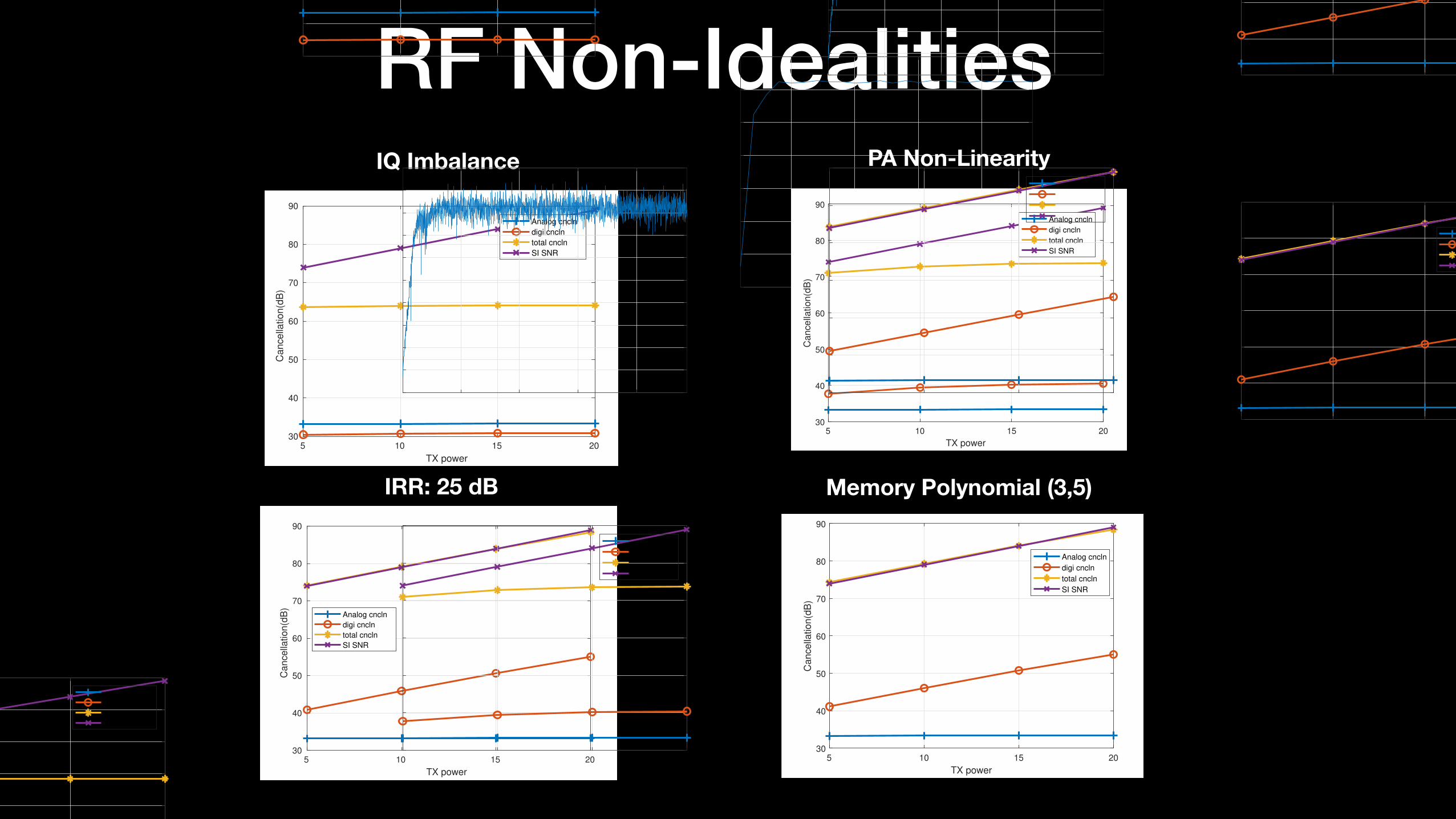
RF Non-Idealities
SI that can be canceled by a radio is limited by its IRR. Similarresults are obtained for an IRR of 30dB which is given inFigure. 3.
In Figure. 4 cancellation is obtained by incorporating theeffects of IQ imbalance into the SI signal model. We observethat with this model the SI signal can be canceled to the noisefloor.
5 10 15 20
TX power
20
30
40
50
60
70
80
90
Ca
nce
llatio
n(d
B)
Analog cncln
digi cncln
total cncln
SI SNR
Fig. 2: Transmit power vs cancellation obtained with a transmitIRR of 25dB. This limits the digital cancellation to 25dB.
5 10 15 20
TX power
30
40
50
60
70
80
90
Ca
nce
llatio
n(d
B)
Analog cncln
digi cncln
total cncln
SI SNR
Fig. 3: Transmit power vs cancellation obtained with a transmitIRR of 30dB. This limits the digital cancellation to 30dB.
B. PA non linearity
The coefficients in the PA model were chosen such thatthe power in the non linear terms were 30 dB below thetransmit power. When the transmit power was 20dBm thepower in the non linear terms were -10dBm. Figure: 7 showsthe cancellation affected by not modeling the effect of non-linearity of the PA and figure Figure: 8 shows the improvementin self-interference cancellation after modeling the effect of thePA non linearity. We observe that we are able to cancel uptothe noise floor with the PA model.
5 10 15 20
TX power
30
40
50
60
70
80
90
Ca
nce
llatio
n(d
B)
Analog cncln
digi cncln
total cncln
SI SNR
Fig. 4: Transmit power vs cancellation obtained with a transmitIRR of 30dB corrected by modeling the effect of IQ imbalancein SI cancellation.
5 10 15 20
nth 10000 samples
10
15
20
25
30
35
40
45
Dig
ital c
an
cella
tion
in d
B
RLS filter convergence
Fig. 5: Convergence of the RLS filter with cancellation aver-aged over 10,000 samples.
C. Joint effect of PA non linearity and IQ imbalance
As mentioned earlier, for the power levels considered,the joint effect of PA non linearity and I/Q imbalance canbe approximately modeled using (15). The cancellation vstransmit power in this case is given in Figure: 9. We observethat the approximate model is sufficient to cancel the self-interference signal to the noise floor.
1) RLS filter: An RLS filter was designed with 24 taps eachused for linear and non-linear basis vectors and single tap firstand second derivatives were modeled. This was sufficient tocancel the self-interference signal to the noise floor for thechannel model considered. A forgetting factor(�) of 0.9995was used for the simulation. The low forgetting factor wasnecessitated by the total number of taps that needed to beestimated. Note that for an RLS filter when � is 0.9995,the number of samples it takes for the memory effect todecay is 1
e is 11�� , which is 2000 samples. To understand the
SI that can be canceled by a radio is limited by its IRR. Similarresults are obtained for an IRR of 30dB which is given inFigure. 3.
In Figure. 4 cancellation is obtained by incorporating theeffects of IQ imbalance into the SI signal model. We observethat with this model the SI signal can be canceled to the noisefloor.
5 10 15 20
TX power
20
30
40
50
60
70
80
90
Cance
llatio
n(d
B)
Analog cncln
digi cncln
total cncln
SI SNR
Fig. 2: Transmit power vs cancellation obtained with a transmitIRR of 25dB. This limits the digital cancellation to 25dB.
5 10 15 20
TX power
30
40
50
60
70
80
90
Cance
llatio
n(d
B)
Analog cncln
digi cncln
total cncln
SI SNR
Fig. 3: Transmit power vs cancellation obtained with a transmitIRR of 30dB. This limits the digital cancellation to 30dB.
B. PA non linearity
The coefficients in the PA model were chosen such thatthe power in the non linear terms were 30 dB below thetransmit power. When the transmit power was 20dBm thepower in the non linear terms were -10dBm. Figure: 7 showsthe cancellation affected by not modeling the effect of non-linearity of the PA and figure Figure: 8 shows the improvementin self-interference cancellation after modeling the effect of thePA non linearity. We observe that we are able to cancel uptothe noise floor with the PA model.
5 10 15 20
TX power
30
40
50
60
70
80
90
Cance
llatio
n(d
B)
Analog cncln
digi cncln
total cncln
SI SNR
Fig. 4: Transmit power vs cancellation obtained with a transmitIRR of 30dB corrected by modeling the effect of IQ imbalancein SI cancellation.
5 10 15 20
nth 10000 samples
10
15
20
25
30
35
40
45
Dig
ital c
ance
llatio
n in
dB
RLS filter convergence
Fig. 5: Convergence of the RLS filter with cancellation aver-aged over 10,000 samples.
C. Joint effect of PA non linearity and IQ imbalance
As mentioned earlier, for the power levels considered,the joint effect of PA non linearity and I/Q imbalance canbe approximately modeled using (15). The cancellation vstransmit power in this case is given in Figure: 9. We observethat the approximate model is sufficient to cancel the self-interference signal to the noise floor.
1) RLS filter: An RLS filter was designed with 24 taps eachused for linear and non-linear basis vectors and single tap firstand second derivatives were modeled. This was sufficient tocancel the self-interference signal to the noise floor for thechannel model considered. A forgetting factor(�) of 0.9995was used for the simulation. The low forgetting factor wasnecessitated by the total number of taps that needed to beestimated. Note that for an RLS filter when � is 0.9995,the number of samples it takes for the memory effect todecay is 1
e is 11�� , which is 2000 samples. To understand the
IQ Imbalance
500 1000 1500 2000
nth 100 samples
0
5
10
15
20
25
30
35
40
45
50
Dig
ital c
an
cella
tion in
dB
RLS filter convergence
Fig. 6: Convergence of the RLS filter, with cancellationaveraged over 100 samples.
5 10 15 20
TX power
30
40
50
60
70
80
90
Cance
llatio
n(d
B)
Analog cncln
digi cncln
total cncln
SI SNR
Fig. 7: Cancellation vs Transmit Power when PA non linearityis not modeled.
convergence behaviour of the designed RLS filter, variationof the digital self-interference cancellation with respect tonumber of samples used for RLS filter estimation was foundout by simulation. This is plotted in figure 5. The cancellationis obtained averaged over 10000 samples. In figure 6 we plotthe cancellation averaged over 100 samples. From these twofigures we can see that the RLS filter converges in about40,000 samples. This corresponds to about 500 µ seconds.
V. CONCLUSION
While a Taylor series approximation results in reduction ofnumber channel coefficients, it does not completely model theself-interference signal as the SI signal is also transformed bythe non-ideal behaviour of RF components. The effect of theseRF impairments in conjunction with the taylor series model isstudied in this work. Simulations were conducted to preciselycontrol and vary the RF impairments and observe the effectof individual impairments in the overall system.
5 10 15 20
TX power
30
40
50
60
70
80
90
Cance
llatio
n(d
B)
Analog cncln
digi cncln
total cncln
SI SNR
Fig. 8: Cancellation vs Transmit Power when PA non linearityis modeled.
5 10 15 20
TX power
30
40
50
60
70
80
90
Cance
llatio
n(d
B)
Analog cncln
digi cncln
total cncln
SI SNR
Fig. 9: Cancellation vs Transmit Power when PA non linearityand IQ imbalance is jointly modeled.
REFERENCES
[1] D. Bharadia, E. McMilin, and S. Katti, “Full duplex radios,” in Proceed-
ings of the ACM SIGCOMM 2013 conference on SIGCOMM. ACM,2013, pp. 375–386.
[2] M. Duarte and A. Sabharwal, “Full-duplex wireless communicationsusing off-the-shelf radios: Feasibility and first results,” in Signals, Systems
and Computers (ASILOMAR), 2010 Conference Record of the Forty
Fourth Asilomar Conference on. IEEE, 2010, pp. 1558–1562.[3] M. Duarte, A. Sabharwal, V. Aggarwal, R. Jana, K. K. Ramakrishnan,
C. W. Rice, and N. K. Shankaranarayanan, “Design and characterizationof a full-duplex multiantenna system for wifi networks,” IEEE Trans-
actions on Vehicular Technology, vol. 63, no. 3, pp. 1160–1177, March2014.
[4] M. Chung, M. S. Sim, J. Kim, D. K. Kim, and C. b. Chae, “Prototypingreal-time full duplex radios,” IEEE Communications Magazine, vol. 53,no. 9, pp. 56–63, September 2015.
500 1000 1500 2000
nth 100 samples
0
5
10
15
20
25
30
35
40
45
50
Dig
ital c
ance
llatio
n in
dB
RLS filter convergence
Fig. 6: Convergence of the RLS filter, with cancellationaveraged over 100 samples.
5 10 15 20
TX power
30
40
50
60
70
80
90
Cance
llatio
n(d
B)
Analog cncln
digi cncln
total cncln
SI SNR
Fig. 7: Cancellation vs Transmit Power when PA non linearityis not modeled.
convergence behaviour of the designed RLS filter, variationof the digital self-interference cancellation with respect tonumber of samples used for RLS filter estimation was foundout by simulation. This is plotted in figure 5. The cancellationis obtained averaged over 10000 samples. In figure 6 we plotthe cancellation averaged over 100 samples. From these twofigures we can see that the RLS filter converges in about40,000 samples. This corresponds to about 500 µ seconds.
V. CONCLUSION
While a Taylor series approximation results in reduction ofnumber channel coefficients, it does not completely model theself-interference signal as the SI signal is also transformed bythe non-ideal behaviour of RF components. The effect of theseRF impairments in conjunction with the taylor series model isstudied in this work. Simulations were conducted to preciselycontrol and vary the RF impairments and observe the effectof individual impairments in the overall system.
5 10 15 20
TX power
30
40
50
60
70
80
90
Cance
llatio
n(d
B)
Analog cncln
digi cncln
total cncln
SI SNR
Fig. 8: Cancellation vs Transmit Power when PA non linearityis modeled.
5 10 15 20
TX power
30
40
50
60
70
80
90
Cance
llatio
n(d
B)
Analog cncln
digi cncln
total cncln
SI SNR
Fig. 9: Cancellation vs Transmit Power when PA non linearityand IQ imbalance is jointly modeled.
REFERENCES
[1] D. Bharadia, E. McMilin, and S. Katti, “Full duplex radios,” in Proceed-
ings of the ACM SIGCOMM 2013 conference on SIGCOMM. ACM,2013, pp. 375–386.
[2] M. Duarte and A. Sabharwal, “Full-duplex wireless communicationsusing off-the-shelf radios: Feasibility and first results,” in Signals, Systems
and Computers (ASILOMAR), 2010 Conference Record of the Forty
Fourth Asilomar Conference on. IEEE, 2010, pp. 1558–1562.[3] M. Duarte, A. Sabharwal, V. Aggarwal, R. Jana, K. K. Ramakrishnan,
C. W. Rice, and N. K. Shankaranarayanan, “Design and characterizationof a full-duplex multiantenna system for wifi networks,” IEEE Trans-
actions on Vehicular Technology, vol. 63, no. 3, pp. 1160–1177, March2014.
[4] M. Chung, M. S. Sim, J. Kim, D. K. Kim, and C. b. Chae, “Prototypingreal-time full duplex radios,” IEEE Communications Magazine, vol. 53,no. 9, pp. 56–63, September 2015.
PA Non-Linearity
IRR: 25 dB Memory Polynomial (3,5)

An Excellent Platform for Full-Duplex Work
RF Blockset + Simulink

Thank You Any Questions/Comments?
Related Documents