PSPICE

Welcome message from author
This document is posted to help you gain knowledge. Please leave a comment to let me know what you think about it! Share it to your friends and learn new things together.
Transcript

PSPICE
What is Spice?
• Spice is the short form of:
– Simulated
– Program with
– Integrated
– Circuit
– Emphasis
PSPICE Programming
• Why PSPICE Programming
• Steps of Programming
• Statements
• Data Statements
• Control Statements
• Example Circuits
Why PSPICE Programming
• Don’t have to draw the circuit
• More control over the parts
• More control over the analysis
• Don’t have to search for parts
• Some SPICE software (HSPICE etc.) don’t have GUI at all
• Quick and efficient
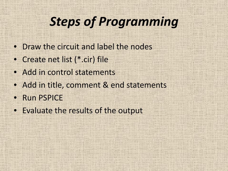
Steps of Programming
• Draw the circuit and label the nodes
• Create net list (*.cir) file
• Add in control statements
• Add in title, comment & end statements
• Run PSPICE
• Evaluate the results of the output
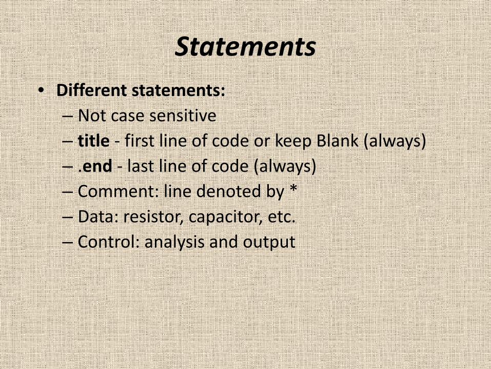
Statements• Different statements:
– Not case sensitive– title ‐ first line of code or keep Blank (always) – .end ‐ last line of code (always)– Comment: line denoted by *– Data: resistor, capacitor, etc.– Control: analysis and output
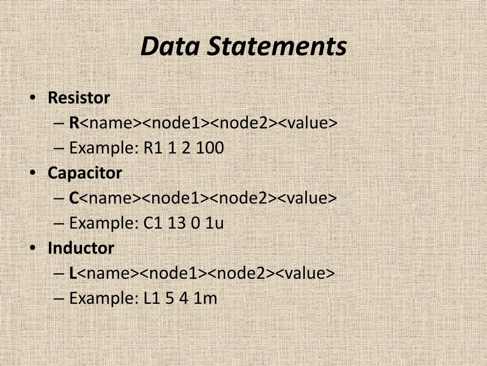
Data Statements
• Resistor– R<name><node1><node2><value>– Example: R1 1 2 100
• Capacitor– C<name><node1><node2><value>– Example: C1 13 0 1u
• Inductor– L<name><node1><node2><value>– Example: L1 5 4 1m
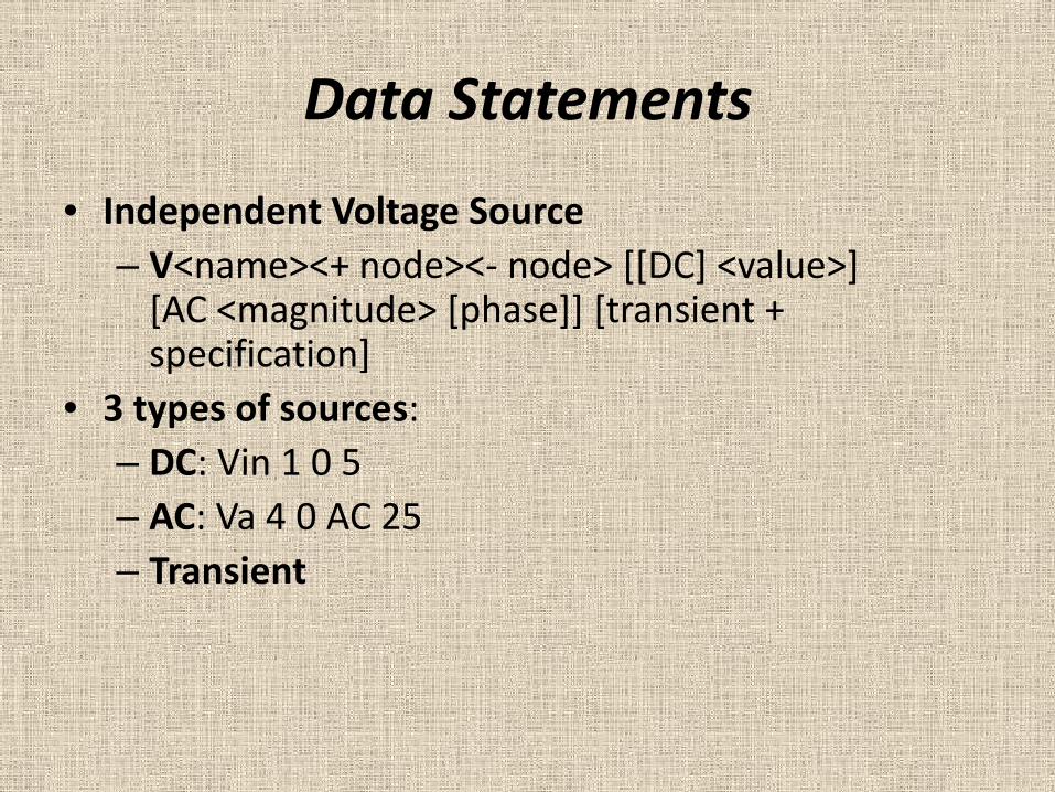
Data Statements
• Independent Voltage Source– V<name><+ node><‐ node> [[DC] <value>] [AC <magnitude> [phase]] [transient + specification]
• 3 types of sources:– DC: Vin 1 0 5– AC: Va 4 0 AC 25– Transient
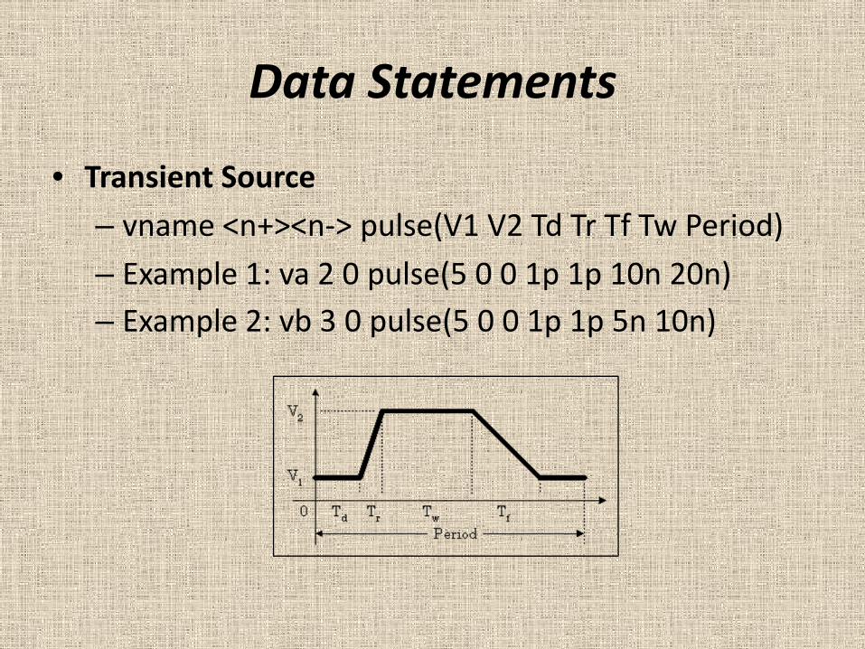
Data Statements
• Transient Source
– vname <n+><n‐> pulse(V1 V2 Td Tr Tf Tw Period)
– Example 1: va 2 0 pulse(5 0 0 1p 1p 10n 20n)– Example 2: vb 3 0 pulse(5 0 0 1p 1p 5n 10n)
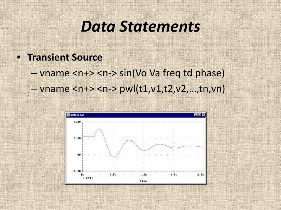
Data Statements
• Transient Source
– vname <n+> <n‐> sin(Vo Va freq td phase)
– vname <n+> <n‐> pwl(t1,v1,t2,v2,…,tn,vn)
Data Statements
• Independent Current Source
– I<name><+ node><‐ node> [[DC] <value>][AC <magnitude> [phase]] [transient + specification]
• Same as Independent Voltage Source
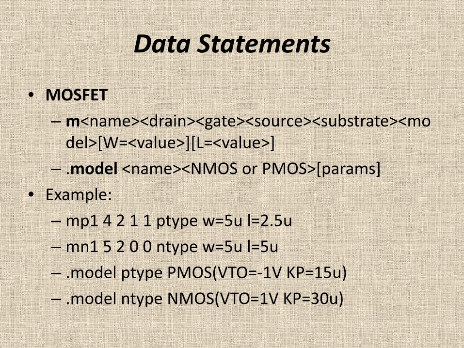
Data Statements
• MOSFET
– m<name><drain><gate><source><substrate><model>[W=<value>][L=<value>]
– .model <name><NMOS or PMOS>[params]
• Example:
– mp1 4 2 1 1 ptype w=5u l=2.5u
– mn1 5 2 0 0 ntype w=5u l=5u
– .model ptype PMOS(VTO=‐1V KP=15u)
– .model ntype NMOS(VTO=1V KP=30u)
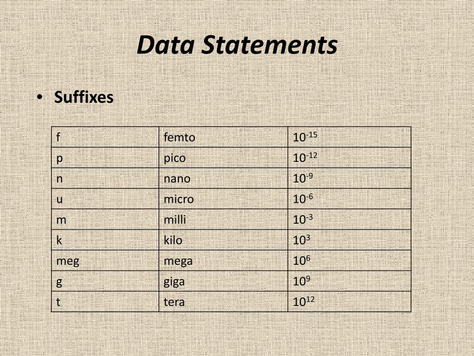
• Suffixes
f femto 10‐15
p pico 10‐12
n nano 10‐9
u micro 10‐6
m milli 10‐3
k kilo 103
meg mega 106
g giga 109
t tera 1012
Data Statements

Control Statements
• Analysis Types
– DC Analysis: .dc
– AC Analysis: .ac
– Transient Analysis: .tran
• Output Format
– Text Output: .print, .plot
– Graph Output: .probe
DC Analysis
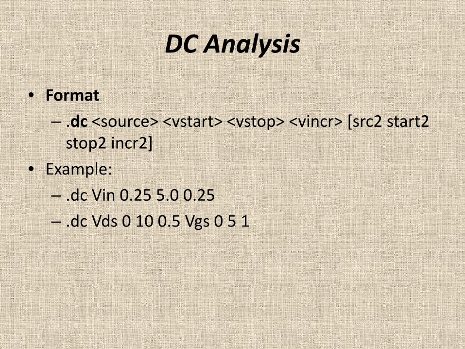
• Format
– .dc <source> <vstart> <vstop> <vincr> [src2 start2 stop2 incr2]
• Example:
– .dc Vin 0.25 5.0 0.25
– .dc Vds 0 10 0.5 Vgs 0 5 1

DC Analysis
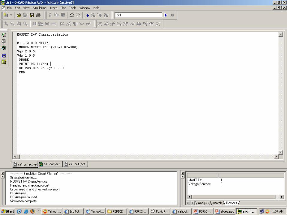
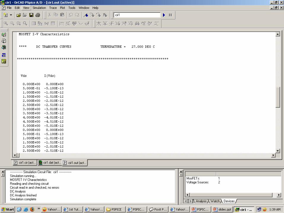
Plot I‐V Characteristics of NMOS
m1 1 2 0 0 ntype.model ntype NMOS(vto=1 kp=30u)vgs 2 0 5vds 1 0 5.probe.print dc i(vds) .dc vds 0 5 .5 vgs 0 5 1.end
ID
G
D
S
1
2
0

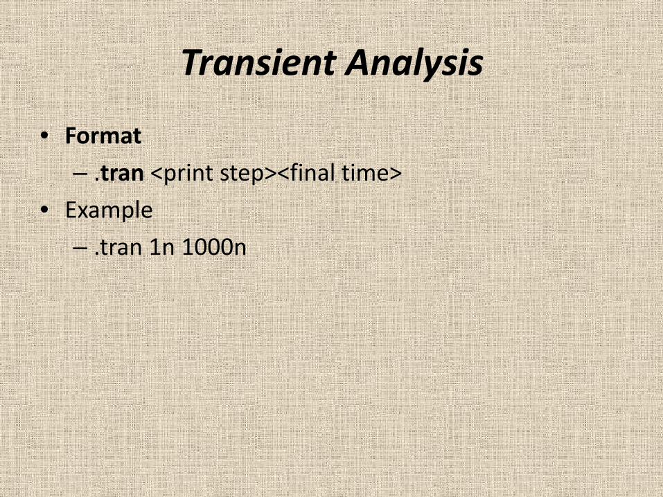
Transient Analysis
• Format
– .tran <print step><final time>
• Example
– .tran 1n 1000n
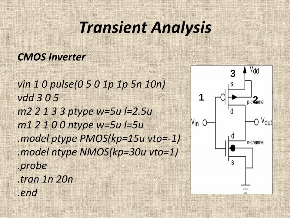
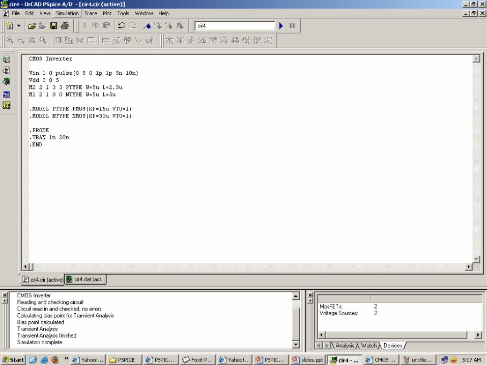
Transient Analysis
CMOS Inverter
vin 1 0 pulse(0 5 0 1p 1p 5n 10n)vdd 3 0 5m2 2 1 3 3 ptype w=5u l=2.5u m1 2 1 0 0 ntype w=5u l=5u.model ptype PMOS(kp=15u vto=‐1).model ntype NMOS(kp=30u vto=1).probe.tran 1n 20n.end
0
2
3
1

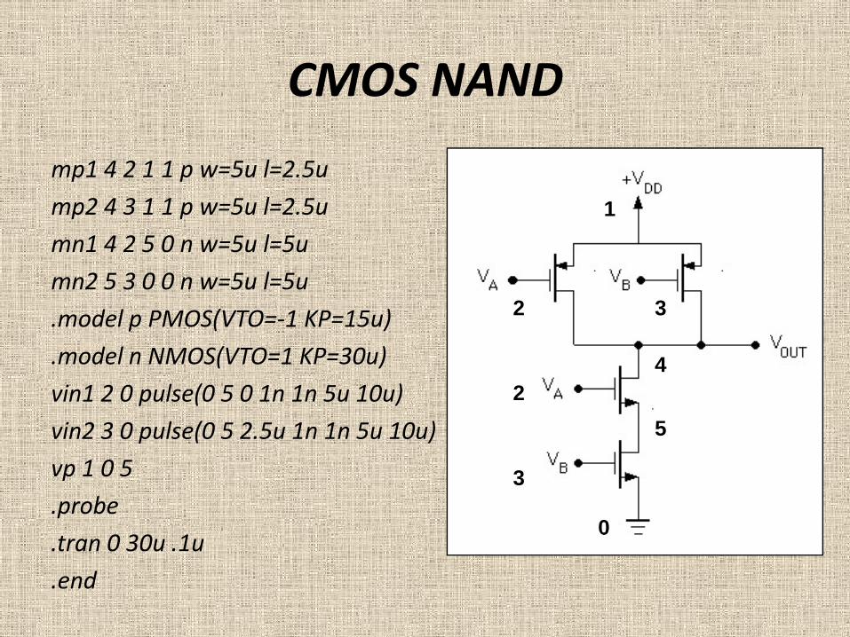
CMOS NAND
mp1 4 2 1 1 p w=5u l=2.5u
mp2 4 3 1 1 p w=5u l=2.5u
mn1 4 2 5 0 n w=5u l=5u
mn2 5 3 0 0 n w=5u l=5u
.model p PMOS(VTO=‐1 KP=15u)
.model n NMOS(VTO=1 KP=30u)
vin1 2 0 pulse(0 5 0 1n 1n 5u 10u)
vin2 3 0 pulse(0 5 2.5u 1n 1n 5u 10u)
vp 1 0 5
.probe
.tran 0 30u .1u
.end
1
2 3
42
3
5
0
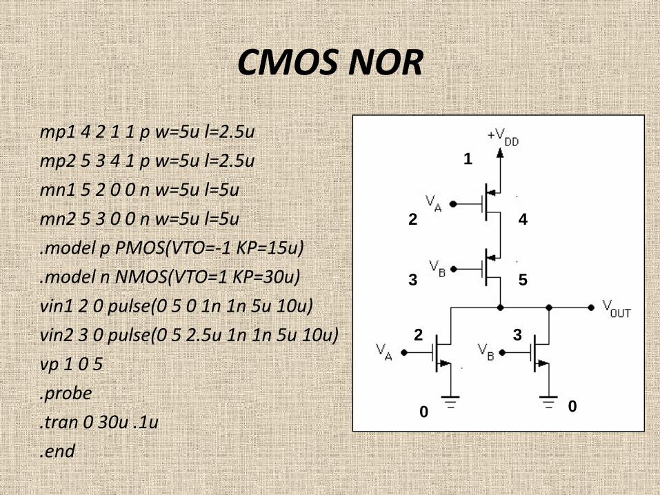
CMOS NOR
mp1 4 2 1 1 p w=5u l=2.5u
mp2 5 3 4 1 p w=5u l=2.5u
mn1 5 2 0 0 n w=5u l=5u
mn2 5 3 0 0 n w=5u l=5u
.model p PMOS(VTO=‐1 KP=15u)
.model n NMOS(VTO=1 KP=30u)
vin1 2 0 pulse(0 5 0 1n 1n 5u 10u)
vin2 3 0 pulse(0 5 2.5u 1n 1n 5u 10u)
vp 1 0 5
.probe
.tran 0 30u .1u
.end
1
2
3
4
5
0 0
2 3
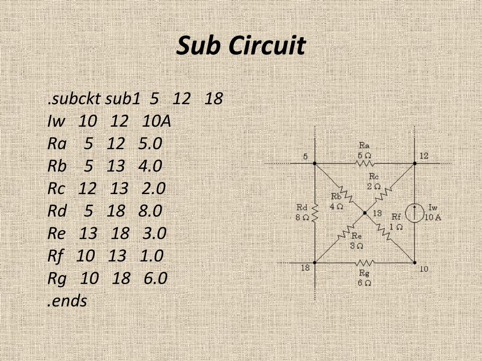
Sub Circuit
.subckt sub1 5 12 18Iw 10 12 10ARa 5 12 5.0Rb 5 13 4.0Rc 12 13 2.0Rd 5 18 8.0Re 13 18 3.0Rf 10 13 1.0Rg 10 18 6.0.ends
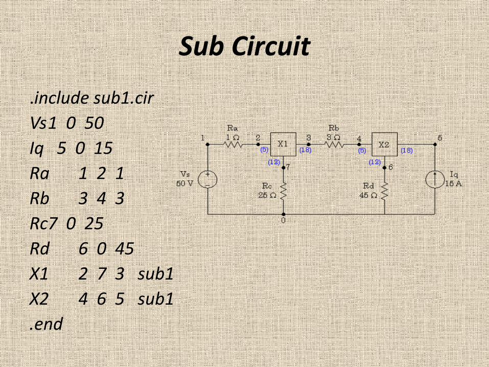
Sub Circuit
.include sub1.cirVs1 0 50Iq 5 0 15Ra 1 2 1Rb 3 4 3Rc7 0 25Rd 6 0 45X1 2 7 3 sub1X2 4 6 5 sub1.end

Thanks
Related Documents