FPGA IMPLEMENTATION OF AN ADAPTIVE HEARING AID ALGORITHM USING BOOTH WALLACE MULTIPLIER A THESIS SUBMITTED IN PARTIAL FULFILLMENT OF THE REQUIREMENTS FOR THE DEGREE OF Master of Technology In VLSI DESIGN and EMBEDDED SYSTEM By NARESH REDDY.N Roll No : 20507001 Department of Electronics & Communication Engineering National Institute of Technology Rourkela 2007

Welcome message from author
This document is posted to help you gain knowledge. Please leave a comment to let me know what you think about it! Share it to your friends and learn new things together.
Transcript

FPGA IMPLEMENTATION OF AN ADAPTIVE HEARING AID ALGORITHM USING BOOTH WALLACE
MULTIPLIER
A THESIS SUBMITTED IN PARTIAL FULFILLMENT
OF THE REQUIREMENTS FOR THE DEGREE OF
Master of Technology
In
VLSI DESIGN and EMBEDDED SYSTEM
By
NARESH REDDY.N Roll No : 20507001
Department of Electronics & Communication Engineering
National Institute of Technology
Rourkela
2007
FPGA IMPLEMENTATION OF AN ADAPTIVE HEARING AID ALGORITHM USING BOOTH WALLACE
MULTIPLIER
A THESIS SUBMITTED IN PARTIAL FULFILLMENT
OF THE REQUIREMENTS FOR THE DEGREE OF
Master of Technology
In
VLSI DESIGN and EMBEDDED SYSTEM
By
NARESH REDDY.N
Under the Guidance of
Prof.K.K.MAHAPATRA
Department of Electronics & Communication Engineering
National Institute of Technology
Rourkela
2007

NATIONAL INSTITUTE OF TECHNOLOGY ROURKELA
CERTIFICATE
This is to certify that the thesis titled “FPGA Implementation of an Hearing Aid Algorithm
Using Booth Wallace Multiplier” submitted by Mr. Naresh Reddy N in partial fulfillment of
the requirements for the award of M.Tech degree in Electronics and Communication Engineering
with specialization “VLSI DESIGN and EMBEDDED SYSTEM” during the session 2006-
2007 at National Institute of Technology, Rourkela (Deemed University) is an authentic work
carried out by him under my supervision and guidance.
To the best of my knowledge, the matter embodied in the thesis has not been submitted to any
other university/institute for the award of any Degree or Diploma.
Prof.K.K.MAHAPATRA
Date: Department of E.C.E National Institute of Technology
Rourkela-769008

CONTENTS
Acknowledgement iv
Abstract vii
List of Figures viii
List of Tables x
1. INTRODUCTION 1
1.1 Motivation 3
1.2 Contributions 3
1.3 Outline 4
2. FUNDAMENTALS OF LOW POWER DESIGN 5
2.1 Design Flow 6
2.2 CMOS Component Model 8
2.2.1 Dynamic power dissipation 8
2.2.2 Static Power Dissipation 12
2.3 Basic Principles of Low Power Design 13
2.3.1 Reduce Voltage and Frequency 14
2.3.2 Reduce capacitance 14
2.3.3 Reduce Leakage and Static Currents 15
3. MULTIPLIERS 16
3.1 Hearing Aid Architecture 17
3.2 Multiplier Background 18
3.3 Speeding up multiplication 20
3.3.1 Sequential multiplier 20
3.3.2 Booth’s Multiplier 21
3.3.3 Wallace multiplier 24
v
3.4 Fast Adders 26

3.4.1 Carry Save Adder Tree 26
3.4.2. Carry Look Ahead Adder (CLA) 27
4. FILTERS 29
4.1 The Adaptive Decorrelator 30
4.2 The Analysis Filter 34
4.3 The Synthesis Filter 37
4.4 High Pass Filter 40
4.5 Analog to Digital Converter 43 4.6 Digital to Analog Converter 44
5. HEARING AID DESIGN 46
5.1 Spectral Sharpening for Speech Enhancement 47
5.2 Spectral Sharpening for Noise Reduction 48
6. DESIGN METHODOLOGY AND SIMULATION RESULTS 51
6.1 The Hardware Description Language 52
6.2 MATLAB Results 56
6.3 VHDL Simulation Results 59
7. CONCLUSION 65
REFERENCES 67
Appendix 69
vi

Acknowledgement
I would like to express my gratitude to my major Prof. K. K. Mahapatra for his
guidance, advice and constant support throughout my thesis work. I would like to thank him for
being my advisor here at National Institute of Technology (Deemed University).
Next, I want to express my respects to Prof. G.S.Rath, Prof. G. Panda, Prof. S.K.
Patra and Dr. S. Meher for teaching me and also helping me how to learn. They have been
great sources of inspiration to me and I thank them from the bottom of my heart.
I would like to thank all faculty members and staff of the Department of Electronics and
Communication Engineering, N.I.T. Rourkela for their generous help in various ways for the
completion of this thesis.
I would also like to mention the names of Jithendra sir, Srikrishna, Balaji, Jagan,
Chaithu, Pandu and Suresh for helping me a lot during the thesis period.
I would like to thank all my friends and especially my classmates for all the thoughtful
and mind stimulating discussions we had, which prompted us to think beyond the obvious. I’ve
enjoyed their companionship so much during my stay at NIT, Rourkela.
I am especially indebted to my parents for their love, sacrifice, and support. They are my
first teachers after I came to this world and have set great examples for me about how to live,
study, and work.
NARESH REDDY N Roll No: 20507001
Dept of ECE, NIT, Rourkela
iv

ABSTRACT
Approximately 10% of the world’s population suffers from some type of hearing loss, yet only
small percentage of this statistic use the hearing aid. The stigma associated with wearing a
hearing aid, customer dissatisfaction with hearing aid performance, the cost and the battery life.
Through the use of digital signal processing the digital hearing aid now offers what the analog
hearing aid cannot offer. It proposes the possibility of flexible gain processing, updating filter
coefficients using adaptive techniques and digital feed back reduction, etc. Currently lot of
attention is being given to low power VLSI design.
Major focus in this thesis is given to the impact of multipliers on the power
consumption of digital hearing aids. At first booth multiplier and booth Wallace multipliers are
designed. The multiplier which consumes less power is taken for designing hearing aid
component. The implementation of the Hearing Aid system includes spectral sharpening for
speech enhancement and spectral sharpening for noise reduction. A fundamental building block,
an adaptive filter, analysis filter, synthesis filter are implemented using Booth multiplier and
Booth Wallace multiplier. The simulation of the hearing aid is done both in MATLAB and
VHDL. The results from MATLAB and VHDL are compared. The hearing aid is constructed,
targeting FPGA. Using the synthesis report and the power calculation report we compare the
relative power consumption of the adaptive decorrelator; analysis filter and synthesis filter for
these multipliers. The results show that the power consumption is reduced using Booth Wallace
multiplier and also that using this multiplier speed is increased. How ever, since the total power
consumption is dominated by the FIR, IIR lattice filters, and the total power saving depends on
the order of the filter.
The hearing aid component is designed in VHDL and implemented in FPGA(VIRTEXII
PRO) kit.
vii

LIST OF FIGURES
Fig no. TITLE Page no. 1.1 Block diagram of hearing aid signal processing 3
2.1 CMOS inverter 9
2.2 CMOS inverter and its transfer curve 11
2.3 Transfer Characteristics of CMOS 11
2.4 Short-circuit current of a CMOS inverter during input transition 12
3.1 The Spectral Sharpening Filter for speech enhancement 17
3.2 Spectral Sharpening for Noise Reduction. 18
3.3 Signed multiplication algorithm 19
3.4 Partial product generation logic 20
3.5 Multiplier bit grouping according to Booth Encoding 22
3.6 Wallace multiplier 25
3.7 Implementation of n bit CSA operation 25
4.1 Block diagram of an adaptive filter 31
4.2 Adaptive gradient lattice decorrelator 32
4.3 Updating the filter coefficients 33
44 Block diagram of the analysis filter [(1-A(z/β)] 35
4.5 Single stage of the analysis filter. 35
4.6 Block diagram of the synthesis filter [1-A(z/γ)]-1 38
4.7 Single stage of the synthesis filter. 39
4.8 The general, causal, length N=M+1, finite-impulse-response 41
4.9 Magnitude response of a high pass FIR filter (cut off frequency 700HZ) 42
4.10 Phase response of a high pass FIR filter (cut off frequency 700HZ). 43
4.11 Impulse response of a high pass FIR filter (cut off frequency 700HZ). 43
5.1 Block diagram of Spectral sharpening for speech enhancement. 47
5.2 Block diagram of Spectral sharpening for noise reduction. 49
6.1 Steps in VHDL or other HDL based design flow 53
viii

6.2 Waveform of the five second speech input 56
6.3 Waveform of the 5 second hearing aid output using parameters β=0.04, γ=0.6, µ=0.98 56
6.4 Waveform of the 5 second hearing aid output using parameters β=0.4, γ=0.6, µ=0.98 57
6.5 Waveform of the 5 second hearing aid output using parameters β=0.04, γ=0.6, µ=0.98 57
6.6 Waveform of the 5 second hearing aid output using parameters β=0.4, γ=0.6, µ=0.98 58
6.7 Waveform of the 5 second hearing aid output using parameters β=0.03, γ=0.7, µ=0.98. 58
6.8 Waveform of the 5 second hearing aid output using parameters β=0.03, γ=0.7, µ=0.98 59
6.9 VirtexIIPRO kit 62
6.10 Hearing aid output in CRO. 62
6.11 Comparison of the input speech signal with the output obtained
using VHDL for 250samples 63
6.12 Comparison of the MATLAB output speech signal with the
output obtained using VHDL for 250 samples 63
6.13 VHDL output of the hearing aid. 64
ix

LIST OF TABLES
Table no. TITLE Page no.
3.1 Booth encoding table 22
3.2 Multiplier recoding for radix-4 booth’s algorithm 23
6.1 Cell Usage for the multipliers in VIRTEXII PRO (XC2VP4-5FF672) 60
6.2 Power consumption and delay for two multipliers with 8X8 bit 60
6.3 Cell Usage for the Hearing Aid Component in VIRTEXII PRO
(XC2VP4-5FF672) 61
x

1
CHAPTER 1
INTRODUCTION

2
Hearing aids are one of many modern, portable, digital systems requiring power efficient
design in order to prolong battery life. Hearing aids perform signal processing functions on
audio signals. With the advent of many new signal processing techniques, their requirement
for higher computational ability has put additional pressure on power consumption. In this
thesis, we are specifically interested on lowering the power consumption of digital hearing
aids. We investigate the use of multipliers for processing audio signals. Through comparison,
we show how the power consumption can be lowered for audio signal processing using
customized multiplier while maintaining the overall signal quality.
Hearing aids are a typical example of a portable device.They includes digital signal
processing algorithms, which demand considerable computing power. Yet, miniature pill
sized batteries store a small amount of energy, limiting their lifetime [7]. Consequently, it is
mandatory to employ low-power design and circuit techniques without neglecting their
impact on area occupation. Hearing impairment is often accompanied with reduced frequency
selectivity which leads to a decreased speech intelligibility in noisy environments. One
possibility to alleviate this deficiency is the spectral sharpening for speech enhancement
based on adaptive filtering [1]; the important frequency contributions for intelligibility
(formants) in the speech are identified and accentuated. Due to area constraints, such
algorithms are usually implemented in totally time-multiplexed architectures, in which
multiple operations are scheduled to run on a few processing units. This work discusses the
power consumption in an FPGA implementation of the speech enhancement algorithm. It
points out that power consumption can be reduced using Booth Wallace multiplier [8].
Several implementations of the algorithm, differing only in the degree of resource sharing are
investigated aiming at power-efficiency maximization. At first an overview of the algorithm
is given. Next the realized architectures are presented.
1.1 MOTIVATION
The need for improved hearing aids is widely attested to by the nationally supported research
efforts worldwide. Over 28 million Americans have hearing impairments severe enough to
cause a communications handicap. While hearing aids are the best means of treatment for the
vast majority of these people, only about 5 million of them own hearing aids, and fewer than
2 million aids are sold annually. Market surveys of hearing aid owners have found that only
slightly more than half (58%) of these people are satisfied with their aids[14].

3
The input signal comes in from the left, is sampled at a rate of 8 kS/s, and is simultaneously
presented to high pass filter and decorrelator. Signal amplification is done using both analysis
filter and synthesis filter.
Figure 1.1 Block diagram of hearing aid signal processing.
1.2 CONTRIBUTIONS
In a digital hearing aid, the resource limitations can be extreme, given that the entire device
(including the battery) needs to fit within the ear canal. As a result, power consumption must
be held to an absolute minimum. In this thesis, we investigate the power savings associated
with constructing the hearing aid using a different multipliers customized to the needs of the
application. Specifically, we compare the relative power consumption of three designs, one
using a shift-add multiplier, Booths multiplier and Booth Wallace multiplier. Each design is
implemented in an FPGA. Since in a channel the total power consumption is dominated by
the FIR, IIR lattice filters, the total power saving depends on the order of the filters.
Our work in this thesis is listed as follows,
1. Implementations of the shift-add multiplier, Booth’s multiplier and Booth Wallace
multiplier in VHDL, with different bit widths.
2. An implementation of a hearing aid channel in MATLAB.
AdaptiveDecorrelator
1-A(z/ )1
1-A(z/ )
K1,k2 ..km
Y[n]
1- z-1
Loudnesscontrol
X[n]

4
3. An implementation of a hearing aid channel using different multipliers in VHDL and
input set on FPGA targets.
4. Comparison of the results obtained using MATLAB and VHDL.
1.3 OUTLINE
This thesis is organized as follows.
Chapter 2 describes the need for low power VLSI design and the factors affecting the power
dissipation in a VLSI chip.
Chapter 3 describes the three Multipliers Shift-Add, Booth’s, Booth Wallace multipliers. Two
adders carry save adder and carry look ahead adder are described.
Chapter 4, we describe the functionality of the Adaptive filter and give a review of the
implementation of the FIR filter, analysis filter and synthesis filter, other fundamental
components in the hearing aid.
Chapter 5, The hearing aid design is presented. Two blocks spectral sharpening for speech
enhancement and spectral sharpening for noise reduction are presented.
Chapter 6, Basic concepts of VHDL and FPGA are given. Simulation results are presented.
Comparison of the hearing aid signal processing using VHDL and MATLAB results are
shown.
Finally, we conclude in Chapter 7.

5
CHAPTER 2FUNDAMENTALS OF LOW POWER
DESIGN

6
Here we discuss ‘power consumption’ and methods for reducing it. Although they may not
explicitly say so, most designers are actually concerned with reducing energy consumption.
This is because batteries have a finite supply of energy (as opposed to power, although
batteries put limits on peak power consumption as well). Energy is the time integral of power;
if power consumption is a constant, energy consumption is simply power multiplied by the
time during which it is consumed. Reducing power consumption only saves energy if the
time required to accomplish the task does not increase too much. A processor that consumes
more power than a competitor's may or may not consume more energy to run a certain
program. For example, even if processor A's power consumption is twice that of processor B,
A's energy consumption could actually be less if it can execute the same program more than
twice as quickly as B.
Therefore, we introduce a metric: energy efficiency. We define the energy efficiency e as the
energy dissipation that is essentially needed to perform a certain function, divided by the
actually used total energy dissipation. The function to be performed can be very broad: it can
be a limited function like a multiply-add operation, but it can also be the complete
functionality of a network protocol. Note that the energy efficiency of a certain function is
independent from the actual implementation and thus independent from the issue whether an
implementation is low power.
It is possible to have two implementations of a certain function that are built with different
building blocks, of which one has high energy efficiency, but dissipates more energy than the
other implementation which has a lower energy efficiency, but is built with low-power
components.
2.1 DESIGN FLOW
The design flow of a system constitutes various levels of abstraction. When a system is
designed with an emphasis on power optimization as a performance goal, then the design
must embody optimization at all levels of the design. In general there are three main levels on
which energy reduction can be incorporated. The system level, the logic level, and the
technological level. For example, at the system level power management can be used to turn
off inactive modules to save power, and parallel hardware may be used to reduce global
interconnect and allow a reduction in supply voltage without degrading system throughput.

7
At the logic level asynchronous design techniques can be used. At the technological level
several optimizations can be applied to chip layout, packaging and voltage reduction.
Low power design problems are broadly classified in to
1. Analysis
2. Optimization
Analysis: These problems are concerned about the accurate estimation of the power or energy
dissipation at different phases of the design process. The purpose is to increase confidence of
the design with the assurance that the power consumption specifications are not violated.
Evidently, analysis techniques differ in their accuracy and efficiency. Accuracy depends on
the availability of design information. In early design phases emphasis is to obtain power
dissipation estimates rapidly with very little available information on the design. As the
design proceeds to reveal lower-level details, a more accurate analysis can be performed.
Analysis techniques also serve as the foundation for design optimization.
Optimization: Optimization is the process of generating the best design, given an
optimization goal, without violating design specifications; an automatic design optimization
algorithm requires a fast analysis engine to evaluate the merits of the design choices. A
decision to apply a particular low power design technique often involves tradeoffs from
different sources pulling in various directions. Major criteria to be considered are the impact
on circuit delays, which directly translates to manufacturing costs. Other factors of chip
design such as design cycle time, testability, quality, reliability, reusability; risk etc may all
be affected by a particular design decision to achieve the low power requirement. The task of
a design engineer is to carefully weigh each design choice with in specification constraints
and select the best implementation.
Before we set to analyze or optimize the power dissipation of a VLSI chip, the basic
understanding of the fundamental circuit theory of power dissipation is imminent. Further is
the summary of the basic power dissipation modes of a digital chip.

8
2.2 CMOS COMPONENT MODEL
Most components are currently fabricated using CMOS technology. Main reasons for this
bias is that CMOS technology is cost efficient and inherently lower power than other
technologies[3].
The sources of energy consumption on a CMOS chip can be classified as
1. STATIC power dissipation, due to leakage current drawn continuously form the power
supply and
2. DYNAMIC power dissipation, due to
- Switching transient current,
- Charging and discharging of load capacitances.
The main difference between them is that dynamic power is frequency dependent, while
static is not. Bias (Pb) and leakage currents (Pl) cause static energy consumption. Short
circuit currents (Psc) and dynamic energy consumption (Pd) is caused by the actual effort of
the circuit to switch.
P = Pd + Psc + Pb + Pl ......................................................................................(2.1)
The contributions of this static consumption are mostly determined at the circuit level. While
statically-biased gates are usually found in a few specialized circuits such as PLAs, their use
has been dramatically reduced in CMOS design. Leakage currents also dissipate static
energy, but are also insignificant in most designs (less than 1%). In general we can say that
careful design of gates generally makes their power dissipation typically a small fraction of
the dynamic power dissipation, and hence will be omitted in further analysis.
2.2.1 Dynamic power dissipation
Dynamic power can be partitioned into power consumed internally by the cell and power
consumed due to driving the load. Cell power is the power used internally by a cell or module
primitive, for example a NAND gate or flip-flop. Load power is used in charging the external
loads driven by the cell, including both wiring and fan out capacitances. So the dynamic
power for an entire chip is the sum of the power consumed by all the cells on the chip and the
power consumed in driving all the load capacitances. During the transition on the input of a

9
CMOS gate both p and n channel devices may conduct simultaneously, briefly establishing a
short from the supply voltage to ground. This effect causes a power dissipation of approx. 10
to 15%.
Figure 2.1: CMOS inverter.
The more dominant component of dynamic power is capacitive power. This component is the
result of charging and discharging parasitic capacitances in the circuit. Every time a
capacitive node switches from ground to Vdd an vice-versa energy is consumed. The
dominant component of energy consumption (85 to 90%) in CMOS is therefore dynamic. A
first order approximation of the dynamic energy consumption of CMOS circuitry is given by
the formula:
Pd = Ceff V 2 f ………………………………………….(2.2)
where Pd is the power in Watts, Ceff is the effective switch capacitance in Farads, V is the
supply voltage in Volts, and f is the frequency of operations in Hertz. The power dissipation
arises from the charging and discharging of the circuit node capacitance found on the output

10
of every logic gate. Every low-to-high logic transition in a digital circuit incurs a voltage
change V, drawing energy from the power supply. Ceff combines two factors C, the
capacitance being charged/discharged, and the activity weighting , which is the probability
that a transition occurs.
Ceff = C.
Short-Circuit Current In CMOS Circuit:
Another component of power dissipation also caused by signal switching called short-circuits
power.
Short-Circuit Current of an Inverter:
Figure shows a simple CMOS inverter operating at Vdd with the transistor threshold voltages
of Vtn and Vtp as marked on the transfer curve. When the input signal level is above Vtn, the
N-transistor is turned on; similarly, when the signal level is below Vtp the P-transistor is
turned on. When the input signal Vi switches, there is a short duration in which the input level
is Vtn and Vtp and both transistors are turned on. This causes a short circuit current from Vdd
to ground and dissipates power. The electrical energy drawn from the source is dissipated as
heat in the P and N transistors.
From the first order analysis of the CMOS transistors model, the time variation of the short-
circuit current during signal transition is shown in the figure. The current is zero when the
inputs signal below Vtn or above Vtp. The current increase as Vi rises beyond Vtn and
decreases as it approaches Vtp. Since the supply voltage is constant, the integration of the
current over time multiplies by the supply voltage is the energy dissipated during the input
transition period.

11
Figure 2.2: CMOS inverter and its transfer curve.
Figure2.3: Transfer Characteristics of CMOS.
Vdd
ip
Vi
ic
C
ip=ic+in
in
Outputvoltage
Vi VdVi
Vd

12
Figure2.4 Short-circuit current of a CMOS inverter during input transition.
2.2.2 Static power dissipation
Strictly speaking, digital CMOS circuits are not supposed to consume static power from
constant static current flow. All non-leakage current in CMOS circuits should only occur in
transient when signals are switching. However, there are times when deviations from CMOS
style circuit design are necessary.
An example is the pseudo NMOS logic. However, for special circuits such as PLAS or
Register files, it may be useful due to its efficient area usage. In such circuits, there is tradeoff
for power and area efficiency.
The pseudo NMOS circuit doesn’t require a p-transistor network and saves half the
transistors required for logic computation as compared to the CMOS logic. The circuit has a
special property that the current only flows when the output is at logic 0.
Vip
Vin
t
Input voltage Vi
ip/in
t
Short-circuit current

13
When the output is at logic1, all the N-transistors are turned off and no static power is
consumed.
Expect leakage current. This property may be exploited in a low power design. If a signal is
known to have very high probability of logic1, say 0.99, it may make sense to implement the
computation in pseudo NMOS logic. Conversely, if the single probability is very close to
zero, we may eliminate the N- transistor network of a CMOS gate and replace it with a load
transistor of N type.
An example where this future can be exploited is the system reset circuitry. The reset signal
has extremely low activation probability (for example, during the power-on phase) which can
benefit from such circuit technique. Other examples where single activation probabilities are
extremely low are: test signals, error detection signals, interrupt signals and exception
handling signals.
2.3 BASIC PRINCIPLES OF LOW POWER DESIGN
Conservation and trade-off are the philosophy behind most low power technique. The
conservation school attempts to reduce power that is wasted with out a due course. The
design skills required are in identifying, analyzing.
This often requires complex trade-offs decisions involving a designer’s overall, intimate
understanding of the design specifications, operating environment and intuition acquired
from past design experience are keys to creative low power techniques.
It should be emphasized that no single low power technique is applicable to all situations.
Design constraints should be viewed from all angles with in the bounds of the design
specification. Low power considerations should be applied at all levels of design abstraction
and design activities. Chip area and speed are the major trade-off considerations but a low
power design decision also affects other aspects such as reliability, testability and design
complexity. Early design decisions have higher impact to the final results and therefore,
power analysis should be initiated early in the design cycle. Maintaining a global view of the
power consumption is important so that a chosen technique does not impose restrictions on
other parts of the system offset its benefits.

14
2.3.1 Reduce Voltage and Frequency
One of the most effective ways of energy reduction of a circuit at the technological level is to
reduce the supply voltage, because the energy consumption drops quadratic ally with the
supply voltage. For example, reducing a supply voltage from 5.0 to 3.3 Volts (a 44%
reduction) reduces power consumption by about 56%. As a result, most processor vendors
now have low voltage versions. The problem that then arises is that lower supply voltages
will cause a reduction in performance. In some cases, low voltage versions are actually 5 Volt
parts that happen to run at the lower voltage. In such cases the system clock must typically be
reduced to ensure correct operation. Therefore, any such voltage reduction must be balanced
against any performance drop. To compensate and maintain the same throughput, extra
hardware can be added. This is successful up to the point where the extra control, clocking
and routing circuitry adds too much overhead [58]. In other cases, vendors have introduced
‘true’ low voltage versions of their processors that run at the same speed as their 5 Volt
counterparts. The majority of the techniques employing concurrency or redundancy incur an
inherent penalty in area, as well as in capacitance and switching activity. If the voltage is
allowed to vary, then it is typically worthwhile to sacrifice increased capacitance and
switching activity for the quadratic power improvement offered by reduced voltage. The
variables voltage and frequency have a trade-off in delay and energy consumption. Reducing
clock frequency f alone does not reduce energy, since to do the same work the system must
run longer. As the voltage is reduced, the delay increases. A common approach to power
reduction is to first increase the performance of the module – for example by adding parallel
hardware, and then reduce the voltage as much as possible so that the required performance is
still reached. Therefore, major themes in many power optimization techniques are to optimize
the speed and shorten the critical path, so that the voltage can be reduced. These techniques
often translate in larger area requirements; hence there is a new trade-off between area and
power.
2.3.2Reduce capacitance
Reducing parasitic capacitance in digital design has always been a good way to improve
performance as well as power. However, a blind reduction of capacitance may not achieve

15
the desired results in power dissipation the real goal is to reduce the product of capacitance
and its witching frequency. Singles with high switching frequency should be routed with
minimum parasitic capacitance to conserve power. Conversely, nodes with large parasitic
capacitance should not be allowed to switch at high frequency. Capacitance reduction can be
achieved at most design abstraction levels: material, process technology, physical design
(floor planning, placement and routing) circuit techniques, transistor sizing, logic
restructuring, and architecture transformation and alternative computation algorithms.
2.3.3 Reduce Leakage and Static CurrentsLeakage current, whether reverse biased junction or sub threshold current, is generally not
very useful in digital design. However, designers often have very little control over the
leakage current of the digital circuit. Fortunately, the leakage power dissipation of a CMOS
digital circuit is several orders of magnitude smaller than the dynamic power. The leakage
power problem mainly appears in very low frequency circuits or ones with “sleep modes”
where dynamic activities are suppressed. Most leakage reduction techniques are applied at
low level design abstraction such as process, device and circuit design. Memory chips that
have very high device density are most susceptible to high leakage power.
Transistor sizing, layout techniques and careful circuit design can reduce static current.
Circuit modules that consume static current should be turned off if not used. Sometimes,
static current depends on the logic state of its output and we can consider reversing the signal
polarity to minimize the probability of static current flow.

16
CHAPTER 3
MULTIPLIERS
17
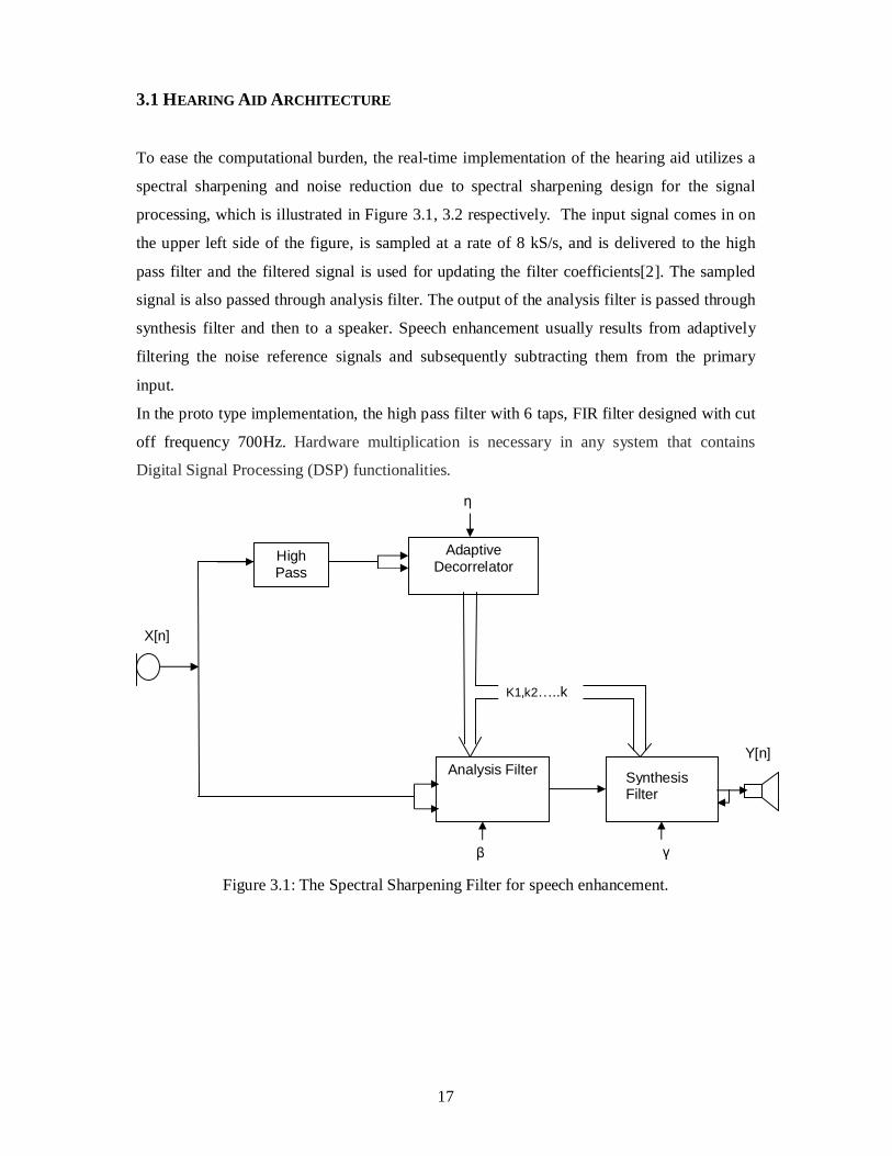
3.1 HEARING AID ARCHITECTURE
To ease the computational burden, the real-time implementation of the hearing aid utilizes a
spectral sharpening and noise reduction due to spectral sharpening design for the signal
processing, which is illustrated in Figure 3.1, 3.2 respectively. The input signal comes in on
the upper left side of the figure, is sampled at a rate of 8 kS/s, and is delivered to the high
pass filter and the filtered signal is used for updating the filter coefficients[2]. The sampled
signal is also passed through analysis filter. The output of the analysis filter is passed through
synthesis filter and then to a speaker. Speech enhancement usually results from adaptively
filtering the noise reference signals and subsequently subtracting them from the primary
input.
In the proto type implementation, the high pass filter with 6 taps, FIR filter designed with cut
off frequency 700Hz. Hardware multiplication is necessary in any system that contains
Digital Signal Processing (DSP) functionalities.
Figure 3.1: The Spectral Sharpening Filter for speech enhancement.
AdaptiveDecorrelator
Analysis Filter
K1,k2 ..km
HighPassfilter
Y[n]
X[n]
SynthesisFilter

18
Figure3.2: Spectral Sharpening for Noise Reduction.
3.2. Multiplier Background
3.2.1. Basic binary multiplier
The shift-add Multiplier scheme is the most basic of unsigned Integer multiplication
algorithms[4].
The operation of multiplication is rather simple in digital electronics. It has its origin from the
classical algorithm for the product of two binary numbers. This algorithm uses addition and
shift left operations to calculate the product of two numbers. Two examples are presented
below.
Basic binary multiplication
The left example shows the multiplication procedure of two unsigned binary digits while the
one on the right is for signed multiplication. The first digit is called Multiplicand and the
second Multiplier. The only difference between signed and unsigned multiplication is that we
AdaptiveDecorrelator
b(1-z -1]
[1-az -1)1-A(z/ )
1
1-A(z/ )
X[n]
K1,k2 ..km
Y[n]

19
have to extend the sign bit in the case of signed one, as depicted in the given right example in
PP row 3. Based upon the above procedure, we can deduce an algorithm for any kind of
multiplication which is shown in Figure 3.3. Here, we assume that the MSB represents the
sign of digit.
Figure 3.3: Signed multiplication algorithm
3.2.2. Partial product generationPartial product generation is the very first step in binary multiplier. These are the
intermediate terms which are generated based on the value of multiplier. If the multiplier bit
is ‘0’, then partial product row is also zero, and if it is ‘1’, then the multiplicand is copied as
it is. From the 2nd bit multiplication onwards, each partial product row is shifted one unit to
the left as shown in the above mentioned example. In signed multiplication, the sign bit is
also extended to the left. Partial product generators for a conventional multiplier consist of a
series of logic AND gates as shown in Figure 3.4.
START
CheckMSB of
Both digits
Final addition
Product
Negative results
Positiveresults
Calculate partial products

20
Figure 3.4: Partial product generation logic
The main operation in the process of multiplication of two numbers is addition of the partial
products. Therefore, the performance and speed of the multiplier depends on the performance
of the adder that forms the core of the multiplier. To achieve higher performance, the
multiplier must be pipelined. Throughput is often more critical than the cycle response in
DSP designs. In this case, latency in the multiply operation is the price for a faster clock rate.
This is accomplished in a multiplier by breaking the carry chain and inserting flip-flops at
strategic locations. Care must be taken that all inputs to the adder are created by signals at the
same stage of the pipeline. Delay at this point is referred to as latency.
3.3 SPEEDING UP MULTIPLICATION
Multiplication involves two basic operations - generation of partial products and their
accumulation. Two ways to speed up multiplication
1. Reducing number of partial products and/or
2. Accelerating accumulation
3.3.1 Sequential multiplier - generates partial products sequentially and adds each newly
generated product to previously accumulated partial product.
Example: add and shift method.
Shift - Adder Multiplier:
Y
X7X6 X5 X4 X3 X2 X1 X0
PP0PP1PP2PP3PP4PP5PP6PP7

21
The following notation is used in our discussion of multiplication algorithms:
a Multiplicand a(k-1)a(k-2) ... a(1)a(0)
x Multiplier x(k-1)x(k-2) ... x(1)x(0)
P Product (a x x) a(2k-1)a(2k-2) ... a(1)a(0)
Sequential or bit-at-a-time multiplication can be done by keeping a cumulative partial product
(initialized to 0) and successively adding to it the properly shifted terms x(j)a. Since each
successive number to be added to the cumulative partial product is shifted by one bit with
respect to the preceding one, a simpler approach is to shift the cumulative partial product by
one bit in order to align its bits with those of the next partial product.
Parallel multiplier - Generates partial products in parallel, accumulates using a fast multi-
operand adder. Number of partial products can be reduced by examining two or more bits of
a multiplier at a time.
Example: Booth’s algorithm reduces number of multiplications to n/2
Where n is the total number of bits in a multiplier
3.3.2Booth’s Multiplier:
In add and shift algorithm the initial partial product is taken as zero. In each step of the
algorithm, LSB bit of the multiplier is tested, discarding the bit which was previously tested,
and hence generating the individual partial products. These partial products are shifted and
added at each step and the final product is obtained after n steps for nxn multiplication. The
main disadvantage of this algorithm is that it can be used only for unsigned numbers[10]. The
range of the input for a ‘n’ bit multiplication is from 0 to 2n-1
A better algorithm which handles both signed and unsigned integers uniformly is Booth’s
algorithm. Booth encoding is a method used for the reduction of the number of partial
products proposed by A.D. Booth in 1950.
X=-2mXm + 2m-1 xm-1 + 2m-2 Xm-2+…….
Rewriting above equation using 2a=2 a+1 -2a leads to
X=-2m(xm-1 –xm)+2m-1(Xm-2+Xm-1)+2m-2(Xm-3-Xm-2)

22
Considering the first 3 bits of X, we can determine whether to add Y, 2Y or 0 to partial
product. The grouping of X bits is shown in Figure 3.5
Figure 3.5: Multiplier bit grouping according to Booth Encoding
The multiplier X is segmented into groups of three bits (Xi+1, Xi, Xi-1) and each group of
bits is associated with its own partial product row using Table 1.
Table3.1 : Booth encoding table
Booth’s algorithm is based on the fact that fewer partial products have to be generated for
groups of consecutive ‘0’ in the multiplier there is no need to generate any new partial
product. For every ‘0’ bit in the multiplier, the previously accumulated partial product needs
only to be shifted by one bit to the right. The above can be implemented by recoding the
multiplier as shown in the table 3.1.
X0 X-1X1X2X3X4X5X6x7
Group0
Group1
Group2
Group3

23
S.NO mri+1 mri mri-1 Recoded digit Operation on the multiplicand
1 0 0 0 0 0 X multiplicand
2 0 0 1 +1 +1 X multiplicand
3 0 1 0 +1 +1 X multiplicand
4 0 1 1 +2 +2 X multiplicand
5 1 0 0 -2 -2 X multiplicand
6 1 0 1 -1 -1 X multiplicand
7 1 1 0 -1 -1 X multiplicand
8 1 1 1 0 0 X multiplicand
Table3.2: Multiplier recoding for radix-4 booth’s algorithm
It is based on portioning the multiplier in to overlapping group of 3- bits and each group is
decoded to generate corresponding partial product. Each recoded digit performs a certain
operation on the multiplicand shown above in the table:3.2
The primary advantage of using this multiplication scheme is that it reduces the number of
partial products generated by half the number.
For example consider 6X6 bit multiplication, number of partial products involved will be 3
where as in Add- Shift algorithm six partial products are needed.
Example :
A 01 00 01 17 Multiplicand
X x 11 01 11 -9 Multiplier
-A +2A -A 0peration
Add –A + 10 11 11
2 bit shift 11 10 11 11
Add 2A 10 00 10
01 11 01 11
2 bit shift 00 01 11 01 11
Add –A + 10 11 11
11 01 10 01 11 -153
24
n/2=3 steps;2 multiplier bits in each step
All shift operations are 2 bit position shifts
Accumulation of the partial products in multiplication is accelerated by adding all the partial
products at a time.
Example:
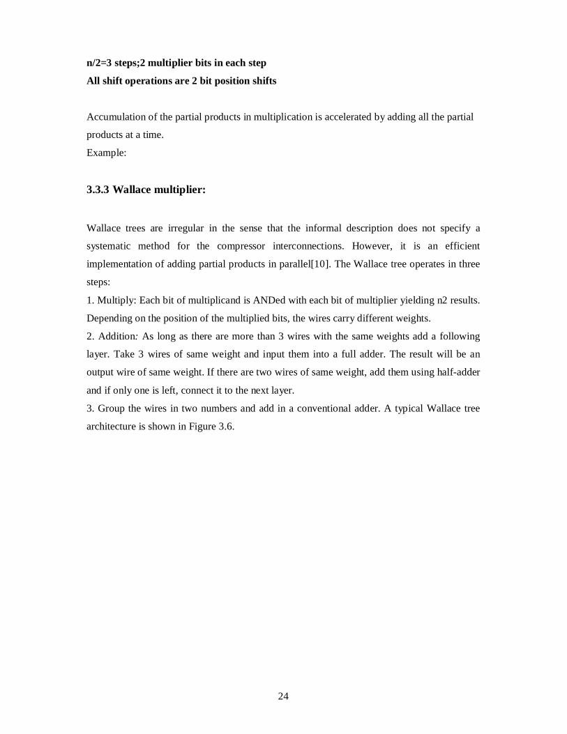
3.3.3 Wallace multiplier:
Wallace trees are irregular in the sense that the informal description does not specify a
systematic method for the compressor interconnections. However, it is an efficient
implementation of adding partial products in parallel[10]. The Wallace tree operates in three
steps:
1. Multiply: Each bit of multiplicand is ANDed with each bit of multiplier yielding n2 results.
Depending on the position of the multiplied bits, the wires carry different weights.
2. Addition: As long as there are more than 3 wires with the same weights add a following
layer. Take 3 wires of same weight and input them into a full adder. The result will be an
output wire of same weight. If there are two wires of same weight, add them using half-adder
and if only one is left, connect it to the next layer.
3. Group the wires in two numbers and add in a conventional adder. A typical Wallace tree
architecture is shown in Figure 3.6.

25
Fig3.6: Wallace multiplier
In the above diagram ABO-AB7 represents the partial products
Wallace multipliers consist of AND-gates, carry save adders and a carry propagate
adder.
Fig3.7: Implementation of n bit CSA operation
The n-bit CSA consists of disjoint full adders (FA’s). It consumes three -bit input vectors and
produces two outputs, i.e., n-bit sum vector S and n-bit carry vector C. Unlike the normal
FULLADDER
FULLADDER
FULLADDER
CoS0C1Sn-2Cn-1
Sn-1C0
CIZoYoXoZn-2Yn-2Xn-2Zn-1Yn-1Xn-1

26
adders [e.g., ripple-carry adder (RCA) and carry-look ahead adder (CLA)], a CSA contains
no carry propagation. Consequently, the CSA has the same propagation delay as only one FA
delay and the delay is constant for any value of n. For sufficiently large n, the CSA
implementation becomes much faster and also relatively smaller in size than the
implementation of normal adders. In Wallace multiplier carry save adders are used, and one
carry propagate adder is used as shown in the figure3.7.The basic idea in Wallace multiplier
is that all the partial products are added at the same time instead of adding one at a time. This
speeds up the multiplication process.
3.4 FAST ADDERS
The final step in completing the multiplication procedure is to add the final terms in the final
adder. This is normally called “Vector-merging” adder. The choice of the final adder depends
on the structure of the accumulation array.
3.4.1 Carry Save Adder Tree (CSAT)
Carry Save Adder (CSA) can be used to reduce the number of addition cycles as well as to
make each cycle faster. Figure 3.7 shows the implementation of the n-bit carry save adder.
Carry save adder is also called a compressor. A full adder takes 3 inputs and produces 2
outputs i.e. sum and carry, hence it is called a 3:2 compressor. In CSA, the output carry is not
passed to the neighboring cell but is saved and passed to the cell one position down. In order
to add the partial products in correct order, Carry save adder tree (CSAT) is used. In carry-
save adder (CSA) architecture, one adds the bits in each column of the first three partial
products independently (by full adders). From there on, the resulting arrays of sum and carry
bits and the next partial product are added by another array of full adders[10]. This continues
until all of the partial products are condensed into one array of sum bits and one array of
carry bits. A fast adder (carry select or look-ahead) is finally used to produce the final
answer. The advantage of this method is the possibility of regular custom layout. The
disadvantage of the CSA method is the amount of delay of producing the final answer.
Because, the critical path is equivalent to first traversing all CSA arrays and then going
through the final fast adder. In contrast, in Wallace tree architecture, all the bits of all of the
partial products in each column are added together in parallel and independent of other
columns. Then, a fast adder is used to produce the final result similar to the CSA method. The

27
advantage of Wallace tree architecture is speed. This advantage becomes more pronounced
for multipliers of bigger than 16 bits. However, building a regular layout becomes a challenge
in this case. It can be seen that changing the Wallace tree multiplier into a
multiplier/accumulator is quite simple. One needs to include the incoming data for
accumulation in the set of partial products at the input of the Wallace tree section; and the
Wallace tree will treat it as another Partial product. Also, merging multiple parallel
multipliers and adders is as simple. It only needs to include all partial product bits in the same
column in the inputs to the Wallace tree adders.
3.4.2. Carry Look Ahead Adder (CLA)
The concept behind the CLA is to get rid of the rippling carry present in a conventional adder
design. The rippling of carry produces unnecessary delay in the circuit. For fast applications,
a better design is required. The carry-look-ahead adder solves this problem by calculating the
carry signals in advance, based on the input signals. It is based on the fact that a carry signal
will be generated in two cases:
(1) when both bits Ai and Bi are 1, or
(2) when one of the two bits is 1 and the carry-in (carry of the previous stage) is 1.
For a conventional adder the expressions for sum and carry signal can be written as follows.
S = A⊕ B ⊕ C …………………………………...(3.1)
C = AB + BC + AC …………………………………..(3.2)
It is useful from an implementation perspective to define S and Co as functions of some
intermediate signals G (generate), D (delete) and P (propagate). G=1 means that a carry bit
will be generated, P=1 means that an incoming carry will be propagated to C0. These signals
are computed as
Gi = Ai.Bi …………………………………………..(3.3)
Pi = Ai ⊕ Bi ………………………………………..(3.4)
We can write S and C0 in terms of G and P.
C0(G,P) = G + PC …………………………………….(3.5)
S(G,P) = P ⊕ C ……………………………………..(3.6)

28
Lets assume that the delay through an AND gate is one gate delay and through an XOR gate
is two gate delays. Notice that the Propagate and Generate terms only depend on the input
bits and thus will be valid after two and one gate delay, respectively. If one uses the above
expression to calculate the carry signals, one does not need to wait for the carry to ripple
through all the previous stages to find its proper value. Let’s apply this to a 4-bit adder to
make it clear.
C1 = G0 + P0.C0 .
C2 = G1 + P1.C1 = G1 + P1.G0 + P1.P0.C0
C3 = G2 + P2.G1 + P2.P1.G0 + P2.P1.P0.C0
C4 = G3 + P3.G2 + P3.P2.G1 + P3P2.P1.G0 + P3P2.P1.P0.C0
Notice that the carry-out bit, Ci+1, of the last stage will be available after four delays (two
gate delays to calculate the Propagate signal and two delays as a result of the AND and OR
gate). The Sum signal can be calculated as follows,
Si = Ai ⊕ Bi ⊕ Ci = Pi⊕ Ci …………………………...(3.7)
The Sum bit will thus be available after two additional gate delays (due to the XOR gate) or a
total of six gate delays after the input signals Ai and Bi have been applied. The advantage is
that these delays will be the same independent of the number of bits one needs to add, in
contrast to the ripple counter. The carry-look ahead adder can be broken up in two modules:
(1) the Partial Full Adder, which generates Si, Pi and Gi and (2) the Carry Look-ahead Logic,
which generates the carry-out bits.

29
CHAPTER 4
FILTERS

30
4.1 THE ADAPTIVE DECORRELATOR
An adaptive filter is a filter which self-adjusts its transfer function according to an optimizing
algorithm. Because of the complexity of the optimizing algorithms, most adaptive filters are
digital filters that perform digital signal processing and adapt their performance based on the
input signal. By way of contrast, a non-adaptive filter has static filter coefficients (which
collectively form the transfer function).
For some applications, adaptive coefficients are required since some parameters of the
desired processing operation (for instance, the properties of some noise signal) are not known
in advance. In these situations it is common to employ an adaptive filter, which uses feedback
to refine the values of the filter coefficients and hence its frequency response.
Generally speaking, the adapting process involves the use of a cost function, which is a
criterion for optimum performance of the filter (for example, minimizing the noise
component of the input), to feed an algorithm, which determines how to modify of the filter
coefficients to minimize the cost on the next iteration. The block diagram, shown in the
following figure 4.1, serves as a foundation for particular adaptive filter realizations, such as
Least Mean Squares (LMS) and Recursive Least Squares (RLS). The idea behind the block
diagram is that a variable filter extracts an estimate of the desired signal.
Applications of adaptive filters
1.Channel equalization
2.Channel identification
3.Noise cancellation
4.Signal prediction
5.Adaptive Feedback Cancellation

31
Figure4.1 Block diagram of an adaptive filter
From the block diagram shown in figure 4.1 we take the following assumptions:
1. The input signal is the sum of a desired signal d(n) and interfering noise v(n)
x(n) = d(n) + v(n) ………………………………………….(4.1)
2. The variable filter has a Finite Impulse Response (FIR) structure. For such structures the
impulse response is equal to the filter coefficients. The coefficients for a filter of order p are
defined as
Wn(0)=[wn(0),wn(1),……….wn(p)] T …………………………….(4.2)
3. The error signal or cost function is the difference between the desired and the estimated
signal.
( ) ( ) ( )^
e n d n d n= − ……………………………………..(4.3)
The variable filter estimates the desired signal by convolving the input signal with the
impulse response. In vector notation this is expressed as
( ) ( )( )^
Tn n X nWd n =
………………………………………..(4.4)
Where
X(n)=[x(n),x(n-1),………..,x(n-p)]T ………………………………..(4.5)
is an input signal vector. Moreover, the variable filter updates the filter coefficients at every
time instant
Wn+1=Wn+ ∆ Wn…………………………………………..(4.6)
Variable filter Wn
UpdateAlgorithm
+X(n) d(n)
-
+
e(n)
nW∆
( )^
d n

32
where ∆ Wn is a correction factor for the filter coefficients. The adaptive algorithm generates
this correction factor based on the input and error signals. LMS and RLS define two different
coefficient update algorithms.
The speech signal to be transmitted is spectrally masked by noise. By using an adaptive filter,
we can attempt to minimize the error by finding the correlation between the noise at the
signal microphone and the (correlated) noise at the reference microphone. In this particular
case the error does not tend to zero as we note the signal d(k) = x(k) + n(k) whereas the input
signal to the filter is x(k) and n(k) does not contain any speech. Therefore it is not possible to
"subtract" any speech when forming e(k) = d(k) - ( )^
d n . Hence in minimising the power of
the error signal e(k) we note that only the noise is removed and e(k) =~ x(k).
Figure 4.2: Adaptive gradient lattice decorrelator
Figure4.2 depicts the structure of the adaptive gradient lattice decorrelator. The illustration
shows three stages only with indices 1, i and m. good results typically require a filter order
m=8…10 for speech sampled at 8KHz[2]. The output signal with vanishing autocorrelation is
computed on the upper signal path by subtracting from the input sample suitable fractions of
the signal values on the lower path.
X[n]
Z -1
+
X
X
+
+
X
X
+
k1 K2 Km
Z -1
+
X
X
+
Z -1

33
The multipliers k1,………..km are iteratively computed
Ki[n]:=Ki[n-1]+ Ki[n] …………………………….(4.7)
every sampling interval n. the details of this process are illustrated in figure 4.3 for the i-th
stage. Input and output values on upper and lower signal path to and from the i-th stage
contribute to the computation of the update value Ki.
Figure4.3: Updating the filter coefficients
Both output values are multiplied with the input values on the opposite path and then
summed up to form the numerator in the subsequent computation of the update value. The
denominator 2 is iteratively computed.2 [n] := . 2 [n-1] + 2 [n] …………………………….(4.8)
+
Z -
1+
X
X
X XX
X
+ +
+ / +
Z -
1
X
Z -1
2
2
ki
Ki
-
+
-
Z -1
Z -1
Z -1

34
The incremental value equals the sum of the two squared input values. The iterative
computation of the denominator defines an exponentially decaying window which
progressively decreases the influence of past contributions[12].
The computationally expensive division yields fast converging filter coefficients Ki
independent of the varying input signal power level. This remarkable property is
indispensable for good enhancement results. It is also clear contrast to simpler algorithms
replacing the division by a multiplication with a small convergence constant 0<µ<<1.
The longest delay through a string of lattice filters extends from the output of the storage
element in the first lattice filter, through a multiplication with the first reflection coefficient,
then through an addition for each stage of the lattice filter until the output is produced in the
final stage. For a large number of lattice filter stages, this longest delay can be reduced by a
lattice filter optimization for speed which defers the final carry propagating addition until
after the final lattice filter stage. This requires the transmission of an additional value
between lattice filter stages. The multiplication process is speeded using booth multiplier and
the accumulation process is done faster using the Wallace multiplier.
4.2THE ANALYSIS FILTER
The analysis filter H(z)=[(1-A(z/ )] is illustrated in figure4.4. Its structure is similar to that
of the adaptive decorrelator shown in fig4.2
The only difference is the multiplication with the filter parameter following every shift
element z-1 on the lower signal path. Furthermore, the analysis filter does not need a separate
circuitry for coefficient update. It instead requires and therefore copies the filter coefficients
k1, k2…..km computed by the unmodified ( =1) filter structure, i.e., the adaptive
decorrelator.

35
Figure 4.4: The analysis filter [(1-A(z/ )].
Figure 4.5: Single stage of the analysis filter.
Km
Z -1+
X
X
+
X Z -1
X
+
X
K1 K2
+
-
+
-
Z -1+
X
X
+
X
+
-
+
-
+
-
-------
+
+
X
X
z-1
fm-1(n)
bm-1(n)
Km
fm(n)
bm(n)

36
The two mathematical equations for the single stage analysis filter is shown below.
1 1
1 1
( ) ( ) ( 1)( ) ( 1) ( )
m m m m
m m m m
f n f n k b nb n b n k f n
− −
− −
= − −
= − −
Some characteristics of the Lattice predictor:
1. It is the most efficient structure for generating simultaneously the forward and backward
prediction errors.
2. The lattice structure is modular: increasing the order of the filter requires adding only one
extra module, leaving all other modules the same.
3. The various stages of a lattice are decoupled from each other in the following sense: The
memory of the lattice (storing b0(n ¡ 1); : : : ; bm¡1(n ¡ 1)) contains orthogonal variables,
thus the information contained in x(n) is splitted in m pieces, which reduces gradually the
redundancy of the signal.
4. The similar structure of the lattice filter stages makes the filter suitable for VLSI
implementation.
Lattice filters typically find use in such applications as predictive filtering, adaptive filtering,
and speech processing. One desirable feature of lattice filters are their use of reflection
coefficients as the filter parameter. Algorithms exist to compute reflection coefficients to
obtain the optimal linear filter for a given filter order. Reflection coefficients have the
additional property that for some applications, the optimal reflection coefficients remain
unchanged when going from a lower order filter to a higher order filter. Thus, when adding
additional filter stages, only the reflection coefficients for the added stages need to be
computed. The straight forward implementation of a lattice filter would be composed of two
multipliers, two adders and a latch per lattice filter stage as shown in figure 4.5. The longest
timing path to the output of a string of lattice filters starts at the multiply of the first lattice
filter stage and propagates through the adders of each lattice filter stage. The delay for an n
stage conventional lattice filter is equal to the delay of one multiply and n CLAs.
The modification with filter parameter causes the analysis filter to produce an output signal
with reduced formants instead of a signal with completely flat spectral envelope as produced
by the adaptive decorrelator.

37
4.3THE SYNTHESIS FILTER
When considering IIR filters, the direct form filter is the common structure of choice. This is
true, in general, because when designing an algorithm which adapts the parameters ak and bk ,
the coefficients of the difference equation, described below, are manipulated directly.
Yk+a1YK-1+…………+amYk-m = b0 Uk+b1 Uk-1+…………+bm Un-m
Some problems exist in using the direct form filter for adaptive applications. First of all,
ensuring stability of a time-varying direct form filter can be a major difficulty. It is often
computationally a burden because the polynomial, A(z), made up of the ak parameters, must
be checked to see if it is minimum phase at each iteration. Even if the stability was assured
during adaptation, round off error causing limit cycles can plague the filter.
Parallel and cascade forms are often used as alternatives for direct form filters. These consist
of an interconnection of first and second order filter sections, whose sensitivity to round off
errors tends to be less drastic than for the direct form filter. Since the filter is broken down
into a factored form, the round off error associated with each factorization only affects that
term. In the direct form filter, the factors are lumped together so that round off error in each
term affects all of the factors in turn.
A larger problem exists for both parallel and cascade forms: the mapping from transfer
function space to parameter space is not unique. Whenever the mapping from the transfer
function space to the parameter space is not unique, additional saddle points in the error
surface appear that would not be present if the mapping had been unique. The addition of
these saddle points can slow down the convergence speed if the parameter trajectories wander
close to these saddle points. For this reason, these filter forms are considered unsuitable for
adaptive filtering.
A tapped-state lattice form has many of the desirable properties associated with common
digital filters and avoids the problems discussed above. Due to the computational structure,
the round off error in this filter is inherently low.
Direct implementation of the IIR filter can lead to instabilities if it is quantized. The filter is
stable using the following structure. The structure of the synthesis filter [1-A(z/ )]-1 is shown
in figure3.6. The synthesis filter also requires and copies the filter coefficients k1,k2,……km
from the adaptive decorrelator at every sampling interval. The structure in figure4.6 also

38
shows a synthesis filter modified by the multiplication with the filter parameter succeeding
every shift element z-1 on the lower signal path. The unmodified synthesis filter ( =1)
restores the original formants in the output when a signal with flat spectral envelope is fed to
its input. The modification with a parameter value less than unity causes the synthesis filter to
produce an output signal with partially restored formants only. The spectral sharpening effect
results from a suitable choice of both filter parameters 0< <1. Experiments with one
adaptive filter only failed in producing satisfactory speech enhancement results.
Figure 4.6: The synthesis filter [1-A(z/ )]-1
Z -1
+
X
X
+
X
+
+
+
-
+Z -1
X
X
+
X
+
+
+
-
Z -1
X
+
X
+
+
Km K2 K1

39
Figure 4.7: Single stage of the synthesis filter.
The two mathematical equations for the single stage synthesis filter is shown below.
1 1
1 1
( ) ( ) ( 1)( ) ( 1) ( )
m m m m
m m m m
f n f n k b ng n g n k f n
− −
− −
= + −
= − −
The computational complexity of a digital filter structure is given by the total number of
multipliers and the total number of two input adders required for its implementation which
roughly provides an indication of its cost of implementation. The synthesis filter is stable if
the magnitudes of all multiplier coefficients in the realization are less than unity.i.e., -
1<Km<1 for m=M,M-1,………
+
+
X
X
Z-1
fm-1(n) fm(n)
gm(n) gm-1(n)
Km

40
4.4 HIGH PASS FILTER
In signal processing, there are many instances in which an input signal to a system contains
extra unnecessary content or additional noise which can degrade the quality of the desired
portion. In such cases we may remove or filter out the useless samples. For example, in the
case of the telephone system, there is no reason to transmit very high frequencies since most
speech falls within the band of 700 to 3,400 Hz. Therefore, in this case, all frequencies above
and below that band are filtered out. The frequency band between 700 and 3,400 Hz, which
isn’t filtered out, is known as the pass band, and the frequency band that is blocked out is
known as the stop band. FIR, Finite Impulse Response, filters are one of the primary types of
filters used in Digital Signal Processing. FIR filters are said to be finite because they do not
have any feedback. Therefore, if you send an impulse through the system (a single spike)
then the output will invariably become zero as soon as the impulse runs through the filter.
There are a few terms used to describe the behavior and performance of FIR filter including
the following:
• Filter Coefficients - The set of constants, also called tap weights, used to multiply
against delayed sample values. For an FIR filter, the filter coefficients are, by
definition, the impulse response of the filter.
• Impulse Response – A filter’s time domain output sequence when the input is an
impulse. An impulse is a single unity-valued sample followed and preceded by zero-
valued samples. For an FIR filter the impulse response of a FIR filter is the set of
filter coefficients.
• Tap – The number of FIR taps, typically N, tells us a couple things about the filter.
Most importantly it tells us the amount of memory needed, the number of calculations
required, and the amount of "filtering" that it can do. Basically, the more taps in a
filter results in better stop band attenuation (less of the part we want filtered out), less
rippling (less variations in the pass band), and steeper roll off (a shorter transition
between the pass band and the stop band).
• Multiply-Accumulate (MAC) – In the context of FIR Filters, a "MAC" is the
operation of multiplying a coefficient by the corresponding delayed data sample and
accumulating the result. There is usually one MAC per tap.

41
Figure 4.8: The general, causal, length N=M+1, finite-impulse-response
Figure4.8 gives the signal flow graph for a general finite-impulse-response filter (FIR). Such
a filter is also called a transversal filter, or a tapped delay line. The implementation is one
example of a direct-form implementation of a digital filter. The impulse response h(n) is
obtained at the output when the input signal is the impulse signal =[1 0 0 0…]. If the kth tap
is denoted bk, then it is obvious from figure3.8 above that the impulse response signal is
given by
In other words, the impulse response simply consists of the tap coefficients, prep ended and
appended by zeros.
Convolution Representation of FIR Filters : Note that the output of the kth delay element in
figure is x(n-k),k=0,1,2…..m , where x(n) is the input signal amplitude at time n. The output
signal y (n) is therefore
Y(n)=b0x(n)+b1x(n-1)+b2x(n-2)+...........+bm x(n-m)
=0
( )M
mm
b x n m=
−∑
= ( ) ( )m
h m x n m∞
=−∞
−∑
=(h * x)(n)
Where we have used the convolution operator * to denote the convolution of h and x, as
defined in above Equation. An FIR filter thus operates by convolving the input signal x(n)

42
with the filter's impulse response h(n).The transfer function of an FIR filter is given by the z
transform of its impulse response.
0
( )M
n nn n
n nH Z h z b z
∞− −
=−∞ =
=∑ ∑@
Thus, the transfer function of every length N=M+1 FIR filter is an Mth-order polynomial in
Z.
The order of a filter is defined as the order of its transfer function. Note from Figure4.8 that
the order is also the total number of delay elements in the filter. When the number of
delay elements in the implementation is equal to the filter order, the filter implementation is
said to be canonical with respect to delay. It is not possible to implement a given transfer
function in fewer delays than the transfer function order, but it is possible (and sometimes
even desirable) to have extra delays.
Figure 4.9 shows the magnitude response of a FIR HIGH PASS FILTER with cutoff
frequency of 700HZ. The sampling frequency considered here is 8000hz. The order of the
filter is five, hence six coefficients are generated. Figure4.10 shows the phase response and
figure 4.11 shows the impulse response of the high pass filter.
Figure 4.9 : Magnitude response of an high pass FIR filter(cut off frequency 700HZ)

43
Figure 4.10: Phase response of a high pass FIR filter (cut off frequency 700HZ).
Figure 4.11: Impulse response of a high pass FIR filter (cut off frequency 700HZ).
4.5 ANALOG TO DIGITAL CONVERTOR.
A device for converting the information contained in the value or magnitude of some
characteristic of an input signal, compared to a standard or reference, to information in the
form of discrete states of a signal, usually with numerical values assigned to the various
combinations of discrete states of the signal. Analog-to-digital (A/D) converters are used to
transform analog information, such as audio signals or measurements of physical variables

44
(for example, temperature, force, or shaft rotation) into a form suitable for digital handling,
which might involve any of these operations: (1) processing by a computer or by logic
circuits, including arithmetical operations, comparison, sorting, ordering, and code
conversion, (2) storage until ready for further handling, (3) display in numerical or graphical
form, and (4) transmission.
If a wide-range analog signal can be converted, with adequate frequency, to an appropriate
number of two-level digits, or bits, the digital representation of the signal can be transmitted
through a noisy medium without relative degradation of the fine structure of the original
signal. Conversion involves quantizing and encoding. Quantizing means partitioning the
analog signal range into a number of discrete quanta and determining to which quantum the
input signal belongs. Encoding means assigning a unique digital code to each quantum and
determining the code that corresponds to the input signal. The most common system is
binary, in which there are 2n quanta (where n is some whole number), numbered
consecutively; the code is a set of n physical two-valued levels or bits (1 or 0) corresponding
to the binary number associated with the signal quantum.
The A-D converter used here is AD9240.
The resolution for this ADC is 14bit; the sampling rate is 10MSP and the input range is 0-5V.
Here the ADC is buffered by using Rail-to-Rail amplifier AD8052. AD8052 is useful in
various applications such as imaging, communications, and medical and data acquisition
systems.
4.6 DIGITAL TO ANALOG CONVERTOR
A device for converting information in the form of combinations of discrete (usually binary)
states or a signal to information in the form of the value or magnitude of some characteristics
of a signal, in relation to a standard or reference. Most often, it is a device which has
electrical inputs representing a parallel binary number, and an output in the form of voltage or
current.
Digital-to-analog (D/A) converters (sometimes called DACs) are used to present the results
of digital computation, storage, or transmission, typically for graphical display or for the
control of devices that operate with continuously varying quantities. D/A converter circuits

45
are also used in the design of analog-to-digital converters that employ feedback techniques,
such as successive-approximation and counter-comparator types. In such applications, the
D/A converter may not necessarily appear as a separately identifiable entity.
The fundamental circuit of most D/A converters involves a voltage or current reference; a
resistive “ladder network” that derives weighted currents or voltages, usually as discrete
fractions of the reference; and a set of switches, operated by the digital input, that determines
which currents or voltages will be summed to constitute the output. The output of the D/A
converter is proportional to the product of the digital input value and the reference.
The device used for D-A conversion is AD-7541A. The resolution for this DAC is 12bit; the
conversion time is 100ns, settling time of 600ns and the analog output range is 0-5v.

46
CHAPTER 5
HEARING AID DESIGN

47
5.1 SPECTRAL SHARPENING FOR SPEECH ENHANCEMENTSpeech enhancement usually results from adaptively filtering the noise reference
signals and subsequently subtracting them from the primary input. How ever, a procedure for
speech enhancement based on a single audio path is presented here. It is there fore applicable
for real world situations. An example of such a situation is using hearing aid equipment. The
hearing impaired person could place additional microphones close to noise sources only
rarely. Current hearing aid equipment comprise filtering and amplifying the speech signal and
thus suggest that hearing impairment is just a more or less reduced sensitivity to sound
pressure in various frequency intervals. This view however neglects the loss of frequency
discrimination which can be efficiently compensated by the spectral sharpening technique
presented. The idea of spectral sharpening originates from the adaptive post filtering method
in modern speech coding schemes at bit rates around 8kb/s and lower. With these algorithms
speech is encoded segment by segment. The linear prediction filter
A(z)=a1z-1 + a2z-2+…..+ amz-m
Is any way computed in every speech segment for the encoding process, and post- filtering with
the transfer function
1 ( )( )
1 ( )
zAH z zA
β
γ
−=
−
and constant filter parameters 0< < <1 is subsequently performed with a moderate
computational increase.
Figure5.1: Block diagram of Spectral sharpening for speech enhancement.
AdaptiveDecorrelator
1-A(z/ )1
1-A(z/ )
K1,k2 ..km
Y[n]
1- z-1
Loudnesscontrol
X[n]

48
Figure5.1 shows the block diagram of spectral sharpening of speech sharpening for speech
enhancement. The speech signal x[n] from the microphone splits into three distinct paths.
The signal on the lowest path passes through the analysis filter [(1-A(z/ )] and subsequently
through the synthesis filter [1-A(z/ )]-1. Both filters are implemented as lattice filters with the
analysis and synthesis structures respectively. They both require the identical set of reflection
coefficients k1,k2,…..km.
m represents the number of stages .
Which is updated every sampling interval by the adaptive decorrelator shown on the middle
path of figure4.1. The filter parameters b and y do not vary with time.
A high pass filter 1- z-1 is shown in front of the adaptive decorrelator, where x=1 may be
chosen for simplicity. The high pass filter is used in order to compensate the spectral tilt of
natural speech: the average power of the speech signal decreases above 1 KHz at a rate of ~ 10
db per octave. The adaptive transfer function
1 ( )( )
1 ( )
zAH z zA
β
γ
−=
−
enhances this spectral tilt even more when the filter coefficients k1,k2,……..km are computed
from the speech signal x[n] directly. Efficient speech enhancement requires however that the
various formants are more or less uniformly emphasized, regardless of their relative power
level. This is possible with the use of the high pass filter. It compensates at least partially the
original spectral tilt.
The decorrelator on the middle signal path of the figure is an adaptive gradient lattice filter. It
produces an output signal with vanishing autocorrelation by updating its filter coefficients
every sampling interval to the continuously changing input signal characteristics. The output
signal is not required in this application, however. The updated filter coefficients k1,k2……km
are of interest only for the use in the analysis and synthesis filter.
5.2 SPECTRAL SHARPENING FOR NOISE REDUCTION
The block diagram of the spectral sharpening process for noise reduction is illustrated in
figure5.2. The arrangement of adaptive decorrelator, analysis and synthesis filters agrees with
the former block diagram in figure 5.1: but there are various differences:

49
1 no loudness control,.
2 the input signal x[n] goes directly to the adaptive decorrelator, and
3 a high pass filter precedes the analysis and synthesis filters.
1
1(1 )1
( ) b zhp az
H z−
−−
−=
The reasons for these differences are as follows: as mentioned in the previous section the
spectral sharpening process
1 ( )( )
1 ( )
zAH z zA
β
γ
−=
−
introduces a signal dependent amplification: signal segments with strong formant structure
are amplified more than segments with a rather flat spectral envelop. In the sequel it is
assumed that back ground noise is the major source for signal degradation and that its
spectrum reveals relatively flat resonances only. Speech segments with strong resonances
clearly profit in this situation. They experience a remarkable amplification compared to noisy
segments. The loudness compensation of the previous block diagram is consequently omitted
in order to preserve this effect.
Figure 5.2: Block diagram of Spectral sharpening for noise reduction.
AdaptiveDecorrelator
b(1-z -1]
[1-az -1)1-A(z/ )
1
1-A(z/ )
X[n]
K1,k2 ..km
Y[n]

50
Best results require that the input signal is directly fed to the adaptive decorrelator. Only
negligible amplification is then applied to noisy signal segments as a consequence of their
assumed approximately flat spectrum. The spectral sharpening process further enhances the
spectral tilt of speech when the filter parameters are estimated from the speech signal without
prior compensation.
The high pass filter which preceded the adaptive decorrelator in the figure 5.1 has been
shifted to the bottom signal path in figure5. 2 in order to avoid the scheme from producing a
dull sound.

51
CHAPTER 6DESIGN METHODOLOGY AND
SIMULATION RESULTS

52
6.1 THE HARDWARE DESCRIPTION LANGUAGE:
As the integrated circuit technology has improved to allow more and more components on a
chip, digital systems have continued to grow in complexity. As digital systems have become
more complex, detailed design of the systems at the gate and flip-flop level has become very
tedious and time consuming. For this reason, use of hardware description languages in the
digital design process continues to grow in importance. A hardware description language
allows a digital design system to be designed and debugged at a higher level before
conversion to the gate and flip-flop level. Use of synthesis CAD tools to do this conversion is
becoming more wide spread. This is analogous to writing software programs in a high level
language such as C and then using a computer to convert the programs to machine language.
The two most popular hardware description languages are VHDL and Verilog.
VHDL is a hardware description language used to describe the behavior and structure of
digital systems. The acronym VHDL stands for VHSIC Hard ware Description Language,
and VHSIC in turn stands for very high speed integrated circuit. However, VHDL is a
general purpose hardware description language, which can be used to describe and simulate
the operation of a wide variety of digital systems, ranging in complexity from a few gates to
an interconnection of many complex integrated circuits. VHDL was originally developed for
the military to allow a uniform method for specifying digital systems. The VHDL language
has since become IEEE standard, and it is widely used in industry.
VHDL can describe a digital system at several different levels- behavioral, dataflow and
structural. For example, a binary adder could be described at the behavioral level in terms of
its function of adding two binary numbers, with out giving any implementation details. The
same adder could be described at the data flow level by giving the logic equations for the
adder. Finally, the adder could be described at the structural level by specifying the
interconnections of the gates that comprise the adder.
VHDL leads naturally to a top-down design methodology, in which the system is first
specified at a high level and tested using a simulator. After the system is debugged at this
level the design can gradually be refined eventually leading to structural description.

53
The language has the following feature:
§ Designs may be decomposed hierarchically
§ Each designs element has both a well-defined interface (for connecting in it other
elements) and a precise behavioral specification (for simulating it).
§ Behavioral specifications can use either an algorithm or an actual hardware structure
to define an element’s operation. For example an element can be defined initially by
an algorithm to allow design verification of higher-level elements that use it: later the
algorithmic definition can be replaced by hardware structure.
§ Concurrency timing and clocking can all be modular. VHDL handles asynchronous as
well as synchronous sequential- circuit structures.
§ The logical operation and timing behavior of a design can be simulated.
While the VHDL language and simulation environment were important innovations by
themselves, VHDL’s utility and popularity took a quantum leap with the commercial
development of VHDL synthesis tools. These programs can create logic – circuit structures
directly from VHDL behavioral description using VHDL, simulate and synthesize anything
from a simple combinational circuit to a complete microprocessor system on chip.
Figure6.1 steps in VHDL or other HDL based design flow
A programmable logic device or PLD is an electronic component used to build digital
circuits. Unlike a logic gate, which has a fixed function, a PLD has an undefined function at
the time of manufacture. Before the PLD can be used in a circuit it must be programmed.
Programmability of logic means that new chip designs can be tested and easily changed
without incurring the huge photo mask costs for chips completed in a semiconductor fab. In
addition, memory-based PLDs can be reprogrammed over and over. Figure 6.1 contains a block
Hierarchy /Block
Coding Simulation /Verification
Compilation
Synthesis Fitting/Place TimingVerification

54
diagram of a hypothetical CPLD. Each of the four logic blocks shown there is the equivalent
of one PLD. However, in an actual CPLD there may be more (or less) than four logic blocks.
Note also that these logic blocks are themselves comprised of macro cells and interconnect
wiring, just like an ordinary PLD.
Unlike the programmable interconnect within a PLD, the switch matrix within a CPLD may
or may not be fully connected. In other words, some of the theoretically possible connections
between logic block outputs and inputs may not actually be supported within a given CPLD.
The effect of this is most often to make 100% utilization of the macro cells very difficult to
achieve. Some hardware designs simply won't fit within a given CPLD, even though there are
sufficient logic gates and flip-flops available.
Because CPLDs can hold larger designs than PLDs, their potential uses are more varied.
They are still sometimes used for simple applications like address decoding, but more often
contain high-performance control-logic or complex finite state machines. At the high-end (in
terms of numbers of gates), there is also a lot of overlap in potential applications with
FPGAs. Traditionally, CPLDs have been chosen over FPGAs whenever high-performance
logic is required. Because of its less flexible internal architecture, the delay through a CPLD
(measured in nanoseconds) is more predictable and usually shorter.
FIELD Programmable Gate Arrays
Field Programmable Gate Arrays (FPGAs) can be used to implement just about any hardware
design. One common use is to prototype a lump of hardware that will eventually find its way
into an ASIC. The development of the FPGA was distinct from the PLD/CPLD. There are
three key parts of its structure: logic blocks, interconnect, and I/O blocks. The I/O blocks
form a ring around the outer edge of the part. Each of these provides individually selectable
input, output, or bi-directional access to one of the general-purpose I/O pins on the exterior of
the FPGA package. Inside the ring of I/O blocks lies a rectangular array of logic blocks. And
connecting logic blocks to logic blocks and I/O blocks to logic blocks is the programmable
interconnect wiring. The FPGA we have used here is VIRTEXII pro.

55
VIRTEXII PRO FPGA
Configurable Logic Blocks (CLBs):
CLB resources include four slices and two 3-state buffers.
Each slice is equivalent and contains:
• Two function generators (F & G)
• Two storage elements
• Arithmetic logic gates
• Large multiplexers
• Wide function capability
• Fast carry look-ahead chain
• Horizontal cascade chain (OR gate)
Configuration
Virtex-II Pro devices are configured by loading the bit stream into internal configuration
memory using one of the following modes:
• Slave-serial mode
• Master-serial mode
• Slave Select MAP mode
• Master Select MAP mode
• Boundary-Scan mode (IEEE 1532)
ORDERING INFORMATION

56
6.2. MATLAB Results
6.2.1 Spectral Sharpening for Speech Enhancement in MATLAB
The speech signal for 5seconds is recorded using wave record function in MATLAB. This
speech signal is sampled at 8 kS/s and is taken as input for the hearing aid design. The
figure6.1 shows the waveform of the five second recorded speech input.
Figure 6.1 Waveform of the five second speech input
The sampled signal is given as input to the hearing aid, spectral sharpening for speech
enhancement shown in figure. The result obtained is shown in the figure and is for the single
stage. Here we can see from the figure 6.2 that the output is almost doubled. The selection of
values effect the spectral sharpening process.
The parameters are =0.04, =0.6,µ=0.98
Figure 6.2 Waveform of the 5 second hearing aid output using parameters
=0.04, =0.6,µ=0.98

57
If =0.4, =0.6,µ=0.98 then for single stage hearing aid design the output is as shown in
figure6.3.
The output obtained is amplified by certain factor which is less than twice.
Figure 6.3 Waveform of the 5 second hearing aid output using parameters
=0.4, =0.6,µ=0.98
Figure6.4 shows the result obtained using 8stages.we can see that the output is amplified by
more than twice. The parameters are =0.04, =0.6,µ=0.98
Figure 6.4 Waveform of the 5 second hearing aid output using parameters
=0.04, =0.6,µ=0.98
As the number of stages increases the amplification factor also increases. From the figure6.2
we can see that using the parameters =0.04, =0.6,µ=0.98 for single stage the output obtained
is almost doubled and using the same parameters for the 8 stages the output obtained is more
than double.

58
If =0.4, =0.6,µ=0.98 then for eight stage hearing aid design the output is as shown in
figure6.5.
The output obtained is amplified by certain factor which is less than twice but greater than
single stage output.
Figure 6.5 Waveform of the 5 second hearing aid output using parameters =0.4, =0.6,µ=0.98
6.1.2 Spectral Sharpening for Noise Reduction
The same input is applied for the noise reduction process as shown in figure. The number of
stages taken is eight. The output obtained using MATLAB for the parameters
=0.03, =0.7,µ=0.98 is shown in figure 6.6
Figure 6.6 Waveform of the 5 second hearing aid output using parameters
=0.03, =0.7,µ=0.98.

59
If =0.3, =0.7,µ=0.98 then for eight stage hearing aid design the output is as shown in
figure6.7.
The output obtained is same as that of the original input speech signal and the only difference
is that noise is reduced.
Figure 6.7 Waveform of the 5 second hearing aid output using parameters
=0.03, =0.7,µ=0.98
6.2 VHDL SIMULATION RESULTS.
6.2.1 Multipliers
The table below compares the cell usage of the three multipliers (SHIFT/ADD, BOOTH’S
and BOOTH WALLACE multiplier) for 8bit by 8bit multiplication and 16bit by 16 bit
multiplication. From the table we can see that the booth Wallace multiplier uses less
hardware compared to that of the shift/add multiplier and booth multiplier. The details are
given in appendix.

60
CELLUSUAGE
Shift/add
multiplier(8x8)
Shift/Add
Multiplier(16x16)
Booth’smultiplier
(8x8)
Booth’smultiplier
(16x16)
BoothWallace
Multiplier(8x8)
BoothWallace
Multiplier(16x16)
BELS 240 1000 333 975 167 697
LUT-1 1 1 0 0 0 0
LUT-2 14 1 37 36 5 9
LUT-3 34 186 28 66 51 234
LUT-4 74 290 116 399 83 328
MUXCY 56 240 64 228 0 0
MUXF5 11 27 14 2 28 126
XOR CY 49 225 61 219 0 0
Table6.1: Cell Usage for the three multipliers in VIRTEXII PRO (XC2VP4-5FF672)
Cellsused
Slices 4-LUT IO Delay
BoothWallace
multiplier
76 139 32 20.62ns
Booth’smultiplier
109 192 32 24.41ns
Table 6.2 Power consumption and delay for two multipliers with 8X8 bits.

61
From the table 6.2 we can see that the using the booth Wallace multiplier consumes less
power compared to the booth multiplier and also that booth Wallace multiplier is faster than
booth multiplier. Hence the Booth Wallace multiplier is used for hearing aid design in
VHDL.
Cells used Slices SliceFlip
Flops
4-LUT logic Shiftregisters
IO
BoothWallace
multiplier
2583 196 4885 4866 19 32
Booth’smultiplier
2684 183 5003 4979 24 32
Table6.3: Cell Usage for the Hearing Aid Component in VIRTEXII PRO (XC2VP4-5FF672)

62
6.8VirtexIIPRO kit
6.9 Hearing aid output in CRO.

63
6.2.2 Spectral Sharpening for Speech Enhancement in vhdl The amplitude values of the speech signal sampled at 8KS/s is rounded to 8 bits and stored in
a text file for VHDL simulation. The hearing aid is designed in VHDL and is tested using
different multipliers.
The first 250 samples are taken as input for the hearing aid in VHDL .The output obtained
through simulation is stored in a text file. The text file is read in MATLAB and is plotted as
shown in the figure6.10. The parameters used in VHDL are =0.04, =0.6, µ=0.98.
6.10 Comparison of the input speech signal with the output obtained using VHDL for 250
samples.

64
Figure 6.11 Comparison of the MATLAB output speech signal with the output obtained using
VHDL for 250 samples.
From the figure we can see that the output obtained using VHDL is slightly less in magnitude
than MATLAB output. This is due to rounding of the values and due to fixed point
multiplication. But from the figure 6.11 we see that the VHDL output follows the MATLAB
output.
Figure6.12 VHDL output of the hearing aid.

65
CHAPTER 7CONCLUSION

66
In this thesis, the power savings associated with constructing a hearing aid using a different
multipliers customized to the needs of the application is investigated.
The hearing aid component for single stage and for multistage are executed in MATLAB. We
can see that the amplification depends on parameters of the analysis and synthesis filters and
also on the number of stages taken to implement the design.
Specifically, we compare the relative power consumption of two designs, one using the
Booth’s multiplier, and the other using Booth Wallace multiplier. Each design is targeted in
to an FPGA implementation. The synthesis report after simulation is used to evaluate relative
power consumption. A hearing aid component, two multipliers, is implemented and
evaluated. The hearing aid channel is also constructed. The implementation using the Booth
Wallace multiplier is shown to provide significant power savings over that of booth
multiplier. The power consumed is more using Booth multiplier than booth Wallace and is
slower, shift/add multiplier is slower and consumes more power than booth Wallace
multiplier. Since the total power consumption is dominated by the FIR, IIR lattice filters, the
total power saving is on the order of the filters. Although the specific results presented for
hearing aid component in VHDL section are limited to a single stage, using the results of
single stage hearing aid in VHDL, we can compute the relative power savings for the hearing
aid for multistage processing.
The VHDL code for hearing aid component is dumped in VIRTEXII PRO kit and analyzed.

67
REFERENCES
1. F.Buergin, F.Carbognani and M.Hediger. Low Power Architecture Trade-offs in a
VLSI Implementation of an Adaptive Hearing Aid Algorithm. In IEEE, pages 558-
561, July 2006.
2. A. Schaub and P. Straub. Spectral sharpening for speech enhancement/noise
reduction. In IEEE Acoustics, Speech and Signal Processing (ICASSP-91), pages
993–996, April 1991.
3. A. P. Chandrakasan and R. W. Brodersen. Low Power Digital CMOS Design. Kluwer
Academic Publishers, Boston, Massachusetts, 1995.
4. A. D. Booth, “A signed binary multiplication technique”, Quart. J.Math., vol. IV, pt.
2, 1951.
5. L. P. Rubinfield, “A proof of the modified booth’s algorithm for multiplication,”
IEEE Trans. Computers, vol. 37, 1988.
6. Edwards,. “Signal Processing Techniques for a DSP Hearing Aid”, IEEE International
Symposium on Circuits and Systems, June 1998.
7. Eric Hemmeter. Reducing power consumption using customized numerical
representations in digital hearing aids. Master’s thesis, Washington University, May
2003.
8. M.J.Liao, C.F.Su, Chang and Allen Wu “A carry select adder optimization technique
for high-performance Booth-encoded Wallace tree multipliers” IEEE International
Symposium on Circuits and Systems 2002.
9. J. Wassner, H. Kaeslin, N. Felber, and W. Fichtner. Waveform coding for low-power
digital filtering of speech data. IEEE Transactions on Signal Processing, 51(6):1656–
1661, June 2003.

68
10. M.J.Liao, C.F.Su, Chang and Allen Wu “A carry select adder optimization technique
for high-performance Booth-encoded Wallace tree multipliers” IEEE International
Symposium on Circuits and Systems 2002.
11. Wallace, C.S., “A suggestion for a fast multiplier”, IEEE Trans. Electron. Compute.,
vol. EC-13, pp. 14-17, 1964.
12. Regalia, Phillip A., Adaptive IIR Filtering in Signal Processing and Control, Marcel
Dekker, Inc., 1995.
13. M. Nayeri and W. Jenkins, 1989, “Alternate realizations of adaptive IIR filters and
properties of their performance surfaces”, IEEE Transactions on Circuits and
Systems, Vol. 36, pp. 485-496.
14. Othman O.Khalifa, M.H Makhtar, and M.S. Baharom, “Hearing Aids System for
Impaired People”, International journal of computing and Information
science,vol.2,no.1, pp 23-26,2004.
15. “Digital system design using VHDL”, Charles H Roth, Jr.Thomson Brooks/Cole.
16. “Principles of CMOS VLSI Design, A Systems perspective”, N.H.E.Weste and
K.Eshraghian. 3rd ed. Pearson education 2003.
17. “Digital integrated circuits”, J.Rabey, 3rd ed. Prentice Hall-2003.
18. J. A. Maxwell and P. M. Zurek, “Reducing acoustic feedback in hearing aids,” IEEE
Trans. Speech Audio Processing, vol. 3, pp. 304–313, July 1993.
19. Sankarayya, N., Roy, K., and Bhattacharya, D. “Algorithms for Low-Power and
High-Speed FIR Filter Realization Using Differential Coefficients”. IEEE Trans. on
Circuits and Systems, Vol. 44, No. 6, pp. 488-497, Jun. 1997.
20. http://www.xilinx.com /

69
APPENDIX
VIRTEXII-PRO DEVICE UTILIZATION SUMMARY
Booth Wallace multiplier
Selected Device : 2vp4ff672-5
Number of Slices: 76 out of 3008 2%
Number of 4 input LUTs: 139 out of 6016 2%
Number of IOs: 32
Number of bonded IOBs: 32 out of 348 9%
Speed Grade: -5
Maximum combinational path delay: 20.621ns
Booth Wallace multiplierSelected Device : 2vp4fg256-5
Number of Slices: 109 out of 3008 3%
Number of 4 input LUTs: 192 out of 6016 3%
Number of IOs: 33
Number of bonded IOBs: 33 out of 140 23%
Maximum combinational path delay: 24.412ns
Highpass filter using BOOTH multiplierSelected Device : 2vp4ff672-5
Number of Slices: 241 out of 3008 8%
Number of Slice Flip Flops: 41 out of 6016 0%
Number of 4 input LUTs: 446 out of 6016 7%
Number of IOs: 25
Number of bonded IOBs: 25 out of 348 7%
Number of GCLKs: 1 out of 16 6%
Minimum period: 61.917ns (Maximum Frequency: 16.151MHz)
Minimum input arrival time before clock: 1.810ns
Maximum output required time after clock: 65.296ns

70
Synthesis filterSelected Device : 2vp4ff672-5
Number of Slices: 175 out of 3008 5%
Number of Slice Flip Flops: 32 out of 6016 0%
Number of 4 input LUTs: 323 out of 6016 5%
Number of IOs: 41
Number of bonded IOBs: 41 out of 348 11%
Number of GCLKs: 1 out of 16 6%
Speed Grade: -5
Minimum period: 83.074ns (Maximum Frequency: 12.037MHz)
Minimum input arrival time before clock: 1.681ns
Maximum output required time after clock: 26.924ns
Updating filter coefficients
Selected Device : 2vp4ff672-5
Number of Slices: 1695 out of 3008 56%
Number of Slice Flip Flops: 104 out of 6016 1%
Number of 4 input LUTs: 3159 out of 6016 52%
Number of IOs: 33
Number of bonded IOBs: 33 out of 348 9%
Number of MULT18X18s: 3 out of 28 10%
Number of GCLKs: 1 out of 16 6%
Speed Grade: -5
Minimum period: 457.801ns (Maximum Frequency: 2.184MHz)
Minimum input arrival time before clock: 257.223ns
Maximum output required time after clock: 4.061ns
Decorrelator filterSelected Device : 2vp4ff672-5
Number of Slices: 164 out of 3008 5%
Number of 4 input LUTs: 292 out of 6016 4%
Number of IOs: 40
Number of bonded IOBs: 40 out of 348 11%
Maximum combinational path delay: 30.211ns

71
Hearing aid using booth’s multiplierSelected Device : 2vp4ff672-5
Number of Slices: 2684 out of 3008 89%
Number of Slice Flip Flops: 183 out of 6016 3%
Number of 4 input LUTs: 5003 out of 6016 83%
Number used as logic: 4979
Number used as Shift registers: 24
Number of IOs: 32
Number of bonded IOBs: 25 out of 348 7%
Number of MULT18X18s: 3 out of 28 10%
Number of GCLKs: 2 out of 16 12%
Speed Grade: -5
Minimum period: 644.955ns (Maximum Frequency: 1.550MHz)
Minimum input arrival time before clock: 3.176ns
Maximum output required time after clock: 76.333ns
Maximum combinational path delay: 4.548ns
Hearing aid using booth Wallace multiplier
Selected Device : 2vp4ff672-5
Number of Slices: 2583 out of 3008 85%
Number of Slice Flip Flops: 196 out of 6016 3%
Number of 4 input LUTs: 4885 out of 6016 81%
Number used as logic: 4866
Number used as Shift registers: 19
Number of IOs: 33
Number of bonded IOBs: 33 out of 348 9%
Number of MULT18X18s: 3 out of 28 10%
Number of GCLKs: 1 out of 16 6%
Minimum period: 605.505ns (Maximum Frequency: 1.652MHz)
Minimum input arrival time before clock: 18.453ns
Maximum output required time after clock: 22.736ns
Related Documents