Printable phosphorescent organic light-emitting devices Sean Xia (SID Member) Kwang-Ohk Cheon Jason J. Brooks (SID Member) Mark Rothman, Tan Ngo Patrick Hett, Raymond C. Kwong Mike Inbasekaran (SID Member) Julie J. Brown (SID Member) Takuya Sonoyama, Masaki Ito Shunichi Seki, Satoru Miyashita Abstract — A new approach to full-color printable phosphorescent organic light-emitting devices (P 2 OLEDs) is reported. Unlike conventional solution-processed OLEDs that contain conjugated poly- mers in the emissive layer, the P 2 OLED’s emissive layer consists of small-molecule materials. A red P 2 OLED that exhibits a luminous efficiency of 11.6 cd/A and a projected lifetime of 100,000 hours from an initial luminance of 500 cd/m 2 , a green P 2 OLED with a luminous efficiency of 34 cd/A and a projected lifetime of 63,000 hours from an initial luminance of 1000 cd/m 2 , a light-blue P 2 OLED with a luminous efficiency of 19 cd/A and a projected lifetime 6000 hours from an initial luminance of 500 cd/m 2 , and a blue P 2 OLED with a luminous efficiency of 6.2 cd/A and a projected lifetime of 1000 hours from an initial luminance of 500 cd/m 2 is presented. Keywords — OLED, PHOLED, solution process, ink-jet printing, phosphorescence, lifetime. DOI # 10.1889/JSID17.2.167 1 Introduction Phosphorescent organic light-emitting devices (PHOLEDs) can achieve up to four times the efficiency of fluorescent OLEDs 1 demonstrating nearly 100% internal quantum effi- ciency. 2 These highly efficient devices provide an enabling technology for portable electronic devices, large-area dis- plays, and lighting panels. The operational stability of blue PHOLEDs has been a challenge to their wide-spread accep- tance for commercial applications although recent progress has been reported. 3 However, through the development of materials and device architectures, red and green PHOLEDs fabricated by vacuum thermal evaporation (VTE) demon- strate sufficiently long lifetimes to meet a number of display applications. For example, highly efficient [~20% external quantum efficiency (EQE)] red and green PHOLEDs exhibiting lifetimes in excess of 200,000 hours at 1000 cd/m 2 with very low driving voltages have been achieved. 4 Table 1 summarizes a subset of the commercial green and red PHOLED performance from Universal Display Corp. The use of VTE and associated processes such as fine shadow masking to achieve high-resolution large-area dis- plays is considered by many in the industry to be technically challenging to scale above Gen 3 or 4 sized motherglass. Solution-processing is an alternate thin-film deposition technique that has the potential to address this challenge in large-scale manufacturing. Until recently, solution-process- ing has been used primarily for polymeric light-emitting devices (PLEDs). Polymeric emissive materials form uni- form films upon solution-casting but they can not be processed by vacuum sublimation due to their high molecular weight. In addition, the low triplet energy of a conventional conju- gated polymer backbone is unsuitable for high-efficiency green and blue PHOLEDs due to quenching of the triplet emission. 5 Therefore, developing materials for solution- processable small-molecule emissive layers with high effi- ciency is desirable. Among various solution-processing techniques, ink-jet printing is of particular interest. This technique has potential for direct-patterning of emissive layers for large-area processing with high resolution. Full- Extended revised version of a paper presented at Display Week 2008 (SID ‘08) held May 20–23, 2008 in Los Angeles, California. S. Xia, K-O. Cheon, J. J. Brooks, M. Rothman, T. Ngo, P. Hett, R. C. Kwong, M. Inbasekaran, and J. J. Brown are with Universal Display Corp., 375 Philips Blvd., Ewing, NJ 08618-1428 U.S.A.; telephone 609/671-0980, fax –0995, e-mail: [email protected]. T. Sonoyama, M. Ito, S. Seki, and S. Miyashita are with Seiko-Epson Corp., 281 Fujimi, Fujimi-machi, Suwa-gun, Nagano 399-0293, Japan. © Copyright 2009 Society for Information Display 1071-0922/09/1702-0167$1.00 TABLE 1 — Commercial green and red PHOLED performance. Journal of the SID 17/2, 2009 167

Welcome message from author
This document is posted to help you gain knowledge. Please leave a comment to let me know what you think about it! Share it to your friends and learn new things together.
Transcript
Printable phosphorescent organic light-emitting devices
Sean Xia (SID Member)Kwang-Ohk CheonJason J. Brooks (SID Member)Mark Rothman, Tan NgoPatrick Hett, Raymond C. KwongMike Inbasekaran (SID Member)Julie J. Brown (SID Member)Takuya Sonoyama, Masaki ItoShunichi Seki, Satoru Miyashita
Abstract — A new approach to full-color printable phosphorescent organic light-emitting devices(P2OLEDs) is reported. Unlike conventional solution-processed OLEDs that contain conjugated poly-mers in the emissive layer, the P2OLED’s emissive layer consists of small-molecule materials. A redP2OLED that exhibits a luminous efficiency of 11.6 cd/A and a projected lifetime of 100,000 hoursfrom an initial luminance of 500 cd/m2, a green P2OLED with a luminous efficiency of 34 cd/A anda projected lifetime of 63,000 hours from an initial luminance of 1000 cd/m2, a light-blue P2OLEDwith a luminous efficiency of 19 cd/A and a projected lifetime 6000 hours from an initial luminanceof 500 cd/m2, and a blue P2OLED with a luminous efficiency of 6.2 cd/A and a projected lifetime of1000 hours from an initial luminance of 500 cd/m2 is presented.
Keywords — OLED, PHOLED, solution process, ink-jet printing, phosphorescence, lifetime.
DOI # 10.1889/JSID17.2.167
1 IntroductionPhosphorescent organic light-emitting devices (PHOLEDs)can achieve up to four times the efficiency of fluorescentOLEDs1 demonstrating nearly 100% internal quantum effi-ciency.2 These highly efficient devices provide an enablingtechnology for portable electronic devices, large-area dis-plays, and lighting panels. The operational stability of bluePHOLEDs has been a challenge to their wide-spread accep-tance for commercial applications although recent progresshas been reported.3 However, through the development ofmaterials and device architectures, red and green PHOLEDsfabricated by vacuum thermal evaporation (VTE) demon-strate sufficiently long lifetimes to meet a number of displayapplications. For example, highly efficient [~20% externalquantum efficiency (EQE)] red and green PHOLEDsexhibiting lifetimes in excess of 200,000 hours at 1000 cd/m2
with very low driving voltages have been achieved.4 Table 1summarizes a subset of the commercial green and redPHOLED performance from Universal Display Corp.
The use of VTE and associated processes such as fineshadow masking to achieve high-resolution large-area dis-plays is considered by many in the industry to be technicallychallenging to scale above Gen 3 or 4 sized motherglass.Solution-processing is an alternate thin-film depositiontechnique that has the potential to address this challenge inlarge-scale manufacturing. Until recently, solution-process-ing has been used primarily for polymeric light-emittingdevices (PLEDs). Polymeric emissive materials form uni-form films upon solution-casting but they can not be processedby vacuum sublimation due to their high molecular weight.In addition, the low triplet energy of a conventional conju-gated polymer backbone is unsuitable for high-efficiencygreen and blue PHOLEDs due to quenching of the tripletemission.5 Therefore, developing materials for solution-processable small-molecule emissive layers with high effi-ciency is desirable. Among various solution-processingtechniques, ink-jet printing is of particular interest. Thistechnique has potential for direct-patterning of emissivelayers for large-area processing with high resolution. Full-
Extended revised version of a paper presented at Display Week 2008 (SID ‘08) held May 20–23, 2008 in Los Angeles, California.
S. Xia, K-O. Cheon, J. J. Brooks, M. Rothman, T. Ngo, P. Hett, R. C. Kwong, M. Inbasekaran, and J. J. Brown are with Universal Display Corp., 375Philips Blvd., Ewing, NJ 08618-1428 U.S.A.; telephone 609/671-0980, fax –0995, e-mail: [email protected].
T. Sonoyama, M. Ito, S. Seki, and S. Miyashita are with Seiko-Epson Corp., 281 Fujimi, Fujimi-machi, Suwa-gun, Nagano 399-0293, Japan.
© Copyright 2009 Society for Information Display 1071-0922/09/1702-0167$1.00
TABLE 1 — Commercial green and red PHOLED performance.
Journal of the SID 17/2, 2009 167
color display prototypes have been demonstrated using thistechnology.6
We have recently reported printable phosphorescentorganic light-emitting devices (P2OLEDs) through solu-tion-processing.7 The emissive layer of the P2OLEDs con-sists of only small-molecule materials. P2OLEDs have thepotential to combine the advantages of small-molecule VTEPHOLEDs, such as high efficiency and long lifetime, withthe advantages of solution-processing such as scalability andefficient material utilization. In this paper, we report on thedevelopment of high-efficiency red, green, and blueP2OLEDs. Device and thin-film properties will be dis-cussed for P2OLED materials fabricated by both spin-coat-ing and ink-jet printing.
2 ExperimentalP2OLEDs discussed in this paper are bottom-emittingdevices fabricated on glass substrates. The solution proc-essed layers described here were deposited using a spin-coating or ink-jet-printing method. The anode used forspin-coating devices was a 120-nm-thick layer of indium tinoxide (ITO) for red and green devices or an 80-nm-thicklayer for blue devices, and the cathode was a bi-layer of LiF(0.7 nm)/aluminum (100 nm) deposited in high vacuum
(<10–7-Torr base pressure). The devices have the followingarchitecture: ITO/HIL/HTL/ EML/BL/ETL/LiF/Al, whereHIL is the hole-injection layer, HTL is the hole-transportlayer, EML is the emissive layer, BL is a blocking layer, andETL is an electron-transport layer. The HIL, HTL, andEML were deposited by solution-processing. The BL andETL were deposited by VTE. The P2OLEDs were encapsu-lated in a dry-nitrogen atmosphere (<1 ppm for H2O andO2) using a glass lid and a UV-cured epoxy edge seal. A CaOgetter was added inside the package to react with any by-products of the epoxy cure and any residual water presentwithin the encapsulated volume.
The electroluminescent (EL) spectra were measuredwith a Photo Research 705 spectrophotometer. The current-density–voltage–luminance (JVL) characteristics weremeasured with a calibrated large-area Si photodiode, aKeithley 236 source measurement unit, and a Keithley 2400source meter. The lifetimes were measured in an in-house-designed lifetest system at a constant dc current drive atroom temperature.
3 Results and discussionMultilayer formation by solution-processing poses signifi-cant challenges because the solvent from the material being
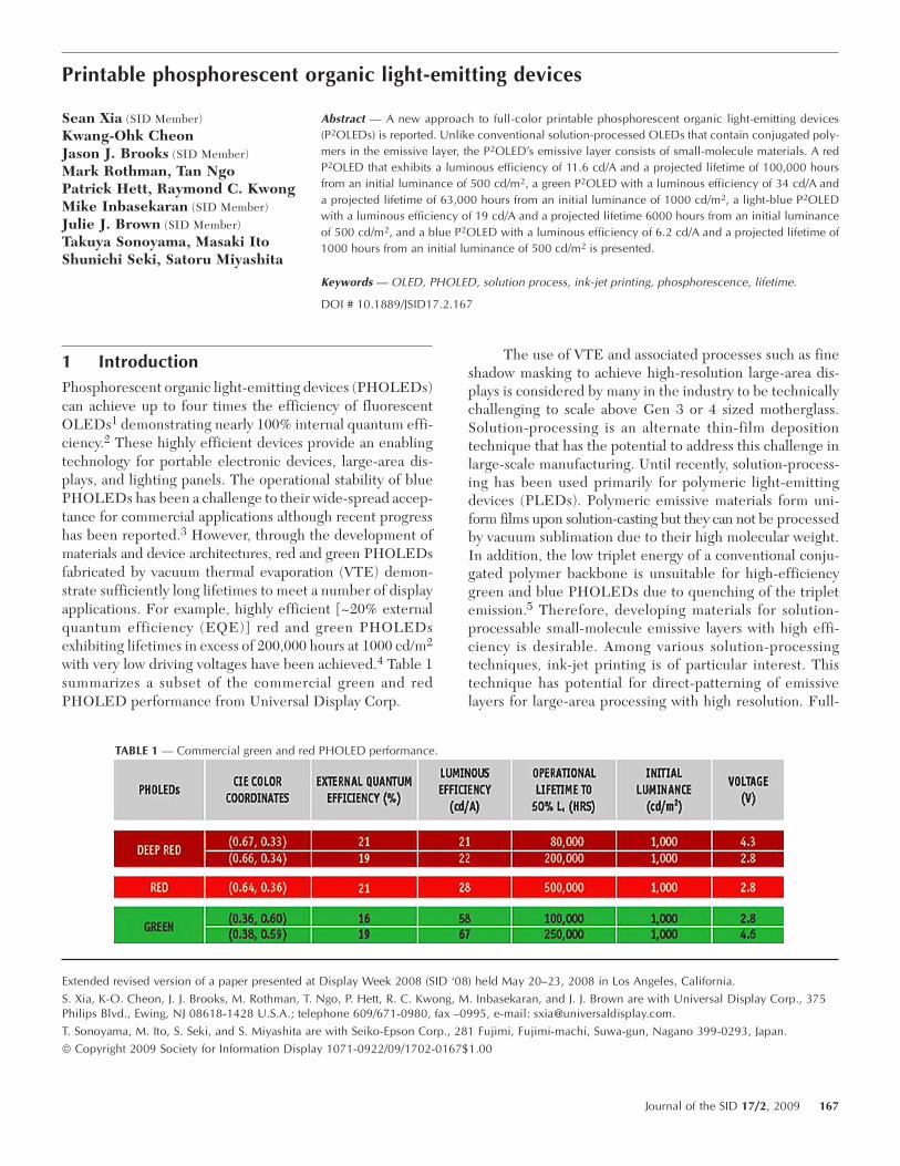
FIGURE 1 — AFM images of spin-coated and VTE films. The dimension of the images is 10 × 10 µm2. (a) VTE HTL on top of thespin-coated HIL; (b) spin-coated HTL on top of spin-coated HIL; (c) VTE EML on top of spin-coated HIL and HTL; (d) spin-coatedEML on top of spin-coated HIL and HTL.
168 Xia et al. / Printable phosphorescent organic LEDs
deposited may dissolve or damage underlying organic lay-ers. Therefore, the preceding organic layer should be ren-dered insoluble to subsequent solution processes. Throughspecific materials design and process optimization, the firstthree layers, i.e., HIL, HTL, and EML, were successfullyfabricated by solution-processing. The surface morpholo-gies of these films were studied by atomic force microscopy(AFM) and compared to analogous vacuum thermal evapo-rated (VTE) films. The results are shown in Fig. 1. Figure1(a) shows the AFM image of a bilayer film with a VTE HTLon top of a spin-coated HIL. The film showed uniform mor-phology with a surface roughness (RMS) of around 1.223nm. The spin-coated HTL on top of spin-coated HIL filmhad a surface roughness with an RMS of around 2.096 nmas shown in Fig. 1(b). Both films showed uniform surfacemorphology. The slightly higher roughness of the spin-coated HTL film may be due to heat treatment after filmformation. The AFM images of Figs. 1(c) and 1(d) comparethe VTE EML and spin-coated EML deposited on spin-coated HIL and HTL, respectively. Interestingly, the sur-face roughness decreased after the spin-coating of theemissive layer when compared to the roughness of theunderlying HTL. The RMS value is around 0.459 nm for thespin-coated EML. The RMS for the VTE EML is around1.636 nm, similar to the roughness of the underlying solu-tion-processed HTL. Both deposition techniques resultedin EML with smooth surfaces without measurable phaseseparation or recrystallization. Phase separation and recrys-tallizaton that occur during film formation is a concern for asmall-molecule host and dopant systems and may result innon-uniform emission pattern and poor device operationallifetime. However, through the careful selection of materi-als, excellent compatibility of amorphous small-moleculehost and dopant can be achieved, allowing for high-qualitysolution-processed films.
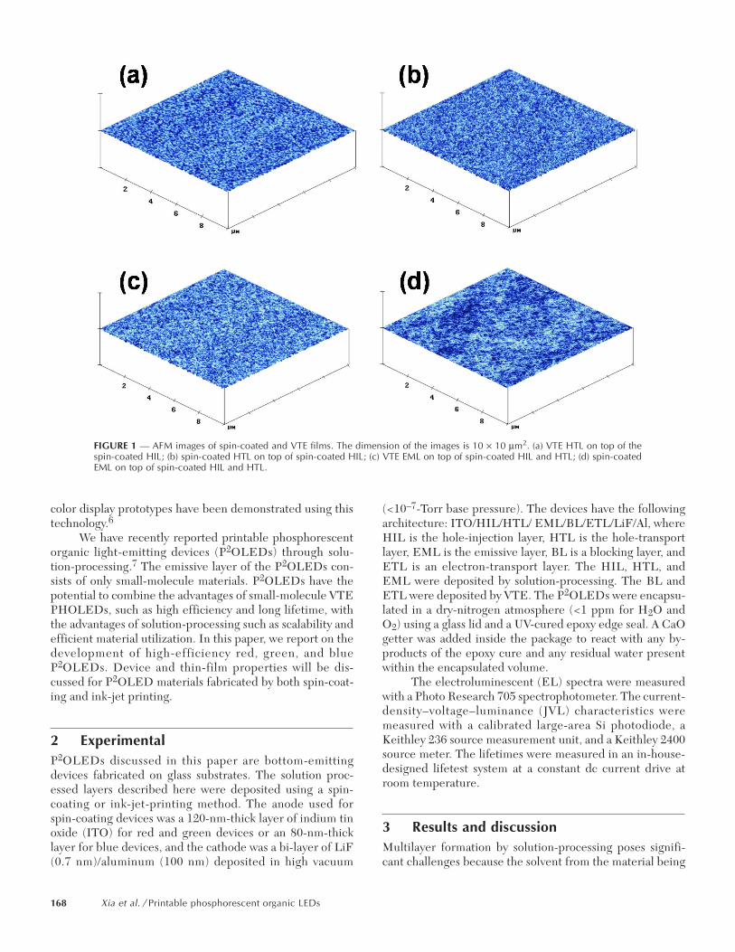
To understand the performance difference betweenVTE devices and solution-processed devices, it is importantto investigate the photophysical properties of the EML. Twoidentical EML films consisting of host and dopant weredeposited on glass substrates using either spin-coating orvacuum thermal evaporation. The photoluminescenceintensity for both films was measured under the same con-ditions. Figure 2 shows the PL intensity of the two films.The solution-processed EML clearly has slightly higher in-tensity compared to the VTE EML. The excited-state life-time of the two films was also measured. The spin-coatedEML had a lifetime of 1.12 µsec and the VTE EML had alifetime of 1.01 µsec. These results indicated that the spin-coated EML has less quenching compared to that of theVTE film. This may be due to better dispersion of thedopant in the spin-coated EML, resulting in less aggrega-tion and less quenching.
Red, green, light-blue, and blue P2OLEDs were fab-ricated by spin-coating. The efficiencies and electrolumi-nescence (EL) spectra are shown in Figs. 3–6. The ELspectra were measured at a current density of 10 mA/cm2.
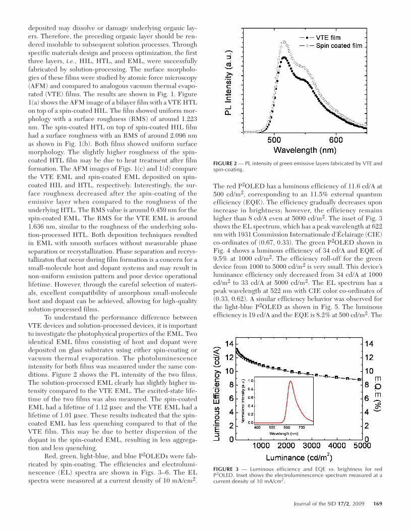
The red P2OLED has a luminous efficiency of 11.6 cd/A at500 cd/m2, corresponding to an 11.5% external quantumefficiency (EQE). The efficiency gradually decreases uponincrease in brightness; however, the efficiency remainshigher than 8 cd/A even at 5000 cd/m2. The inset of Fig. 3shows the EL spectrum, which has a peak wavelength at 622nm with 1931 Commission Internationale d’Éclairage (CIE)co-ordinates of (0.67, 0.33). The green P2OLED shown inFig. 4 shows a luminous efficiency of 34 cd/A and EQE of9.5% at 1000 cd/m2. The efficiency roll-off for the greendevice from 1000 to 5000 cd/m2 is very small. This device’sluminance efficiency only decreased from 34 cd/A at 1000cd/m2 to 33 cd/A at 5000 cd/m2. The EL spectrum has apeak wavelength at 522 nm with CIE color co-ordinates of(0.33, 0.62). A similar efficiency behavior was observed forthe light-blue P2OLED as shown in Fig. 5. The luminousefficiency is 19 cd/A and the EQE is 8.2% at 500 cd/m2. The
FIGURE 2 — PL intensity of green emissive layers fabricated by VTE andspin-coating.
FIGURE 3 — Luminous efficiency and EQE vs. brightness for redP2OLED. Inset shows the electroluminescence spectrum measured at acurrent density of 10 mA/cm2.
Journal of the SID 17/2, 2009 169
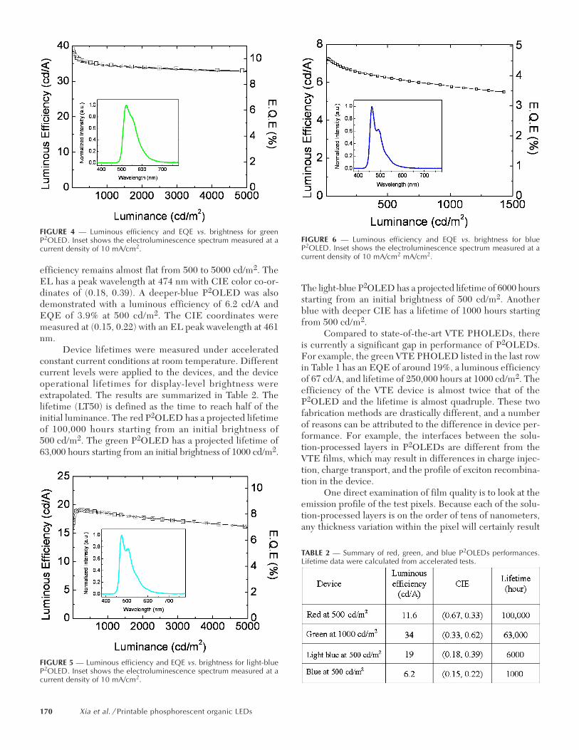
efficiency remains almost flat from 500 to 5000 cd/m2. TheEL has a peak wavelength at 474 nm with CIE color co-or-dinates of (0.18, 0.39). A deeper-blue P2OLED was alsodemonstrated with a luminous efficiency of 6.2 cd/A andEQE of 3.9% at 500 cd/m2. The CIE coordinates weremeasured at (0.15, 0.22) with an EL peak wavelength at 461nm.
Device lifetimes were measured under acceleratedconstant current conditions at room temperature. Differentcurrent levels were applied to the devices, and the deviceoperational lifetimes for display-level brightness wereextrapolated. The results are summarized in Table 2. Thelifetime (LT50) is defined as the time to reach half of theinitial luminance. The red P2OLED has a projected lifetimeof 100,000 hours starting from an initial brightness of500 cd/m2. The green P2OLED has a projected lifetime of63,000 hours starting from an initial brightness of 1000 cd/m2.
The light-blue P2OLED has a projected lifetime of 6000 hoursstarting from an initial brightness of 500 cd/m2. Anotherblue with deeper CIE has a lifetime of 1000 hours startingfrom 500 cd/m2.
Compared to state-of-the-art VTE PHOLEDs, thereis currently a significant gap in performance of P2OLEDs.For example, the green VTE PHOLED listed in the last rowin Table 1 has an EQE of around 19%, a luminous efficiencyof 67 cd/A, and lifetime of 250,000 hours at 1000 cd/m2. Theefficiency of the VTE device is almost twice that of theP2OLED and the lifetime is almost quadruple. These twofabrication methods are drastically different, and a numberof reasons can be attributed to the difference in device per-formance. For example, the interfaces between the solu-tion-processed layers in P2OLEDs are different from theVTE films, which may result in differences in charge injec-tion, charge transport, and the profile of exciton recombina-tion in the device.
One direct examination of film quality is to look at theemission profile of the test pixels. Because each of the solu-tion-processed layers is on the order of tens of nanometers,any thickness variation within the pixel will certainly result
FIGURE 4 — Luminous efficiency and EQE vs. brightness for greenP2OLED. Inset shows the electroluminescence spectrum measured at acurrent density of 10 mA/cm2.
FIGURE 5 — Luminous efficiency and EQE vs. brightness for light-blueP2OLED. Inset shows the electroluminescence spectrum measured at acurrent density of 10 mA/cm2.
FIGURE 6 — Luminous efficiency and EQE vs. brightness for blueP2OLED. Inset shows the electroluminescence spectrum measured at acurrent density of 10 mA/cm2 mA/cm2.
TABLE 2 — Summary of red, green, and blue P2OLEDs performances.Lifetime data were calculated from accelerated tests.
170 Xia et al. / Printable phosphorescent organic LEDs

in non-uniform emission pattern. Figure 7 shows the imagesof red, green, and light-blue 6.35-mm2 P2OLED test pixels.In each case, the P2OLEDs showed uniform emission with-out any bright spots or dark area, indicating that the solu-tion-processed layers are of high quality as confirmed byAFM studies.
Although the results of P2OLED performances arenot yet competitive with state-of-the-art VTE PHOLEDs,the improvement in device performance has been signifi-cant, considering the short development period. Figure 8shows the lifetime progress of red, green, and light-blueP2OLEDs over the past 1.5 years. As can be seen, for redP2OLEDs, lifetime has improved five times, from 20,000hours in January 2007 to 100,000 hours in May 2008. Thelifetime of green P2OLEDs improved from 6000 hours to63,000 hours during this same period, and the lifetime oflight blue P2OLEDs improved from 1000 to 6000 hours.With better understanding of the device operational anddegradation mechanisms and with continued improvementin materials and fabrication processes, device performancesare expected to improve even further to meet entry com-mercial requirements.
P2OLEDs have also been demonstrated by using ink-jet-printing technology. One of the key advantages of usingsmall-molecule ink is the versatility of solvent selection andink formulation. Unlike polymer inks, whose viscosity increasesdramatically with increasing concentration, the viscosity ofsmall-molecule inks varies only slightly over a wide concen-tration range. This feature makes small-molecule systemsvery suitable for ink-jet printing. Figure 9 shows the thick-ness profile measured by a surface profilometer of the solu-
FIGURE 7 — Emission images of red, green, and blue P2OLEDs testpixels fabricated by spin-coating, each are 6.35 mm2 in area.
FIGURE 8 — Lifetime progress for (a) red, (b) green, and (c) light-blueP2OLEDs.
FIGURE 9 — Thickness profile of ink-jet-printed layers of a greenP2OLED.
Journal of the SID 17/2, 2009 171
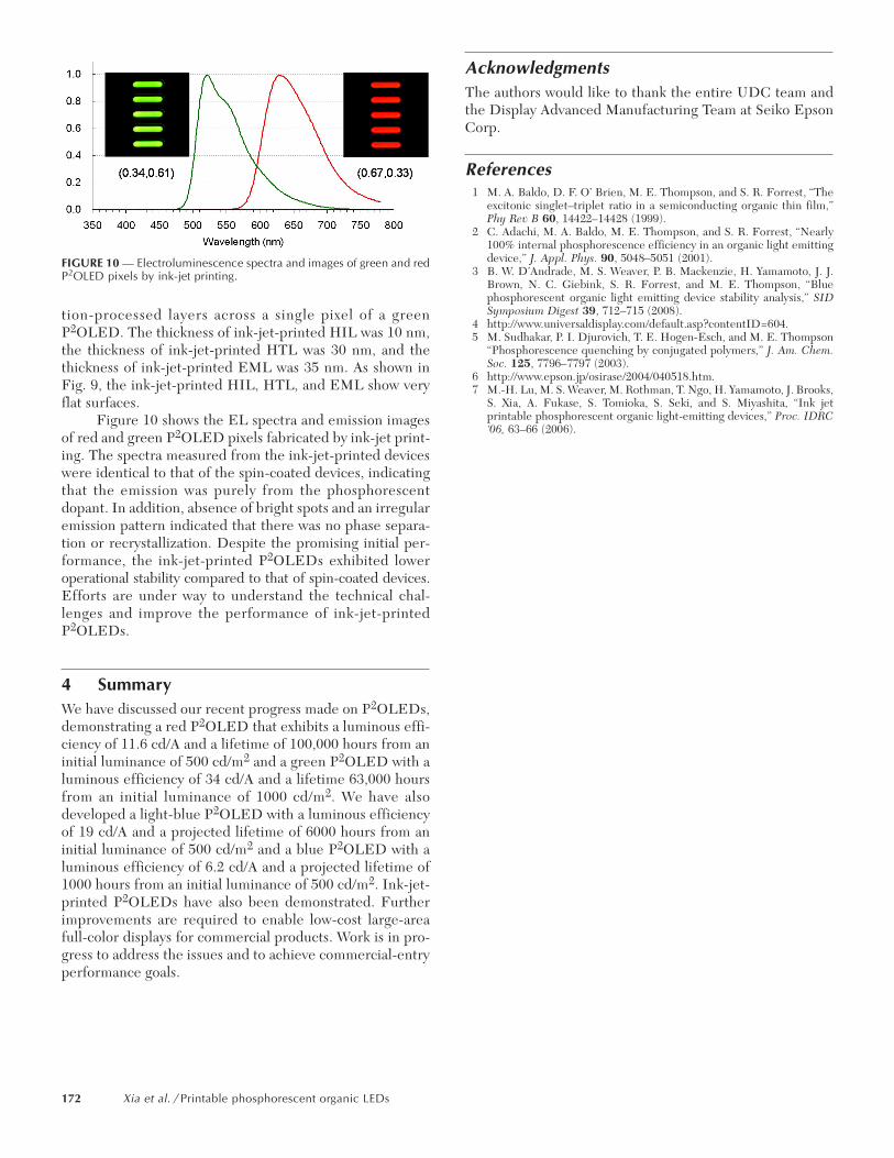
tion-processed layers across a single pixel of a greenP2OLED. The thickness of ink-jet-printed HIL was 10 nm,the thickness of ink-jet-printed HTL was 30 nm, and thethickness of ink-jet-printed EML was 35 nm. As shown inFig. 9, the ink-jet-printed HIL, HTL, and EML show veryflat surfaces.
Figure 10 shows the EL spectra and emission imagesof red and green P2OLED pixels fabricated by ink-jet print-ing. The spectra measured from the ink-jet-printed deviceswere identical to that of the spin-coated devices, indicatingthat the emission was purely from the phosphorescentdopant. In addition, absence of bright spots and an irregularemission pattern indicated that there was no phase separa-tion or recrystallization. Despite the promising initial per-formance, the ink-jet-printed P2OLEDs exhibited loweroperational stability compared to that of spin-coated devices.Efforts are under way to understand the technical chal-lenges and improve the performance of ink-jet-printedP2OLEDs.
4 SummaryWe have discussed our recent progress made on P2OLEDs,demonstrating a red P2OLED that exhibits a luminous effi-ciency of 11.6 cd/A and a lifetime of 100,000 hours from aninitial luminance of 500 cd/m2 and a green P2OLED with aluminous efficiency of 34 cd/A and a lifetime 63,000 hoursfrom an initial luminance of 1000 cd/m2. We have alsodeveloped a light-blue P2OLED with a luminous efficiencyof 19 cd/A and a projected lifetime of 6000 hours from aninitial luminance of 500 cd/m2 and a blue P2OLED with aluminous efficiency of 6.2 cd/A and a projected lifetime of1000 hours from an initial luminance of 500 cd/m2. Ink-jet-printed P2OLEDs have also been demonstrated. Furtherimprovements are required to enable low-cost large-areafull-color displays for commercial products. Work is in pro-gress to address the issues and to achieve commercial-entryperformance goals.
AcknowledgmentsThe authors would like to thank the entire UDC team andthe Display Advanced Manufacturing Team at Seiko EpsonCorp.
References1 M. A. Baldo, D. F. O’ Brien, M. E. Thompson, and S. R. Forrest, “The
excitonic singlet–triplet ratio in a semiconducting organic thin film,”Phy Rev B 60, 14422–14428 (1999).
2 C. Adachi, M. A. Baldo, M. E. Thompson, and S. R. Forrest, “Nearly100% internal phosphorescence efficiency in an organic light emittingdevice,” J. Appl. Phys. 90, 5048–5051 (2001).
3 B. W. D’Andrade, M. S. Weaver, P. B. Mackenzie, H. Yamamoto, J. J.Brown, N. C. Giebink, S. R. Forrest, and M. E. Thompson, “Bluephosphorescent organic light emitting device stability analysis,” SIDSymposium Digest 39, 712–715 (2008).
4 http://www.universaldisplay.com/default.asp?contentID=604.5 M. Sudhakar, P. I. Djurovich, T. E. Hogen-Esch, and M. E. Thompson
“Phosphorescence quenching by conjugated polymers,” J. Am. Chem.Soc. 125, 7796–7797 (2003).
6 http://www.epson.jp/osirase/2004/040518.htm.7 M.-H. Lu, M. S. Weaver, M. Rothman, T. Ngo, H. Yamamoto, J. Brooks,
S. Xia, A. Fukase, S. Tomioka, S. Seki, and S. Miyashita, “Ink jetprintable phosphorescent organic light-emitting devices,” Proc. IDRC‘06, 63–66 (2006).
FIGURE 10 — Electroluminescence spectra and images of green and redP2OLED pixels by ink-jet printing.
172 Xia et al. / Printable phosphorescent organic LEDs
Related Documents

![Light Emitting Devices - Royal Society of ChemistryS1 Supporting Information Phenanthro[9,10-d]triazole and imidazole Derivatives: High Triplet Energy Host Materials for Blue Phosphorescent](https://static.cupdf.com/doc/110x72/611184481156272d2b22c9fc/light-emitting-devices-royal-society-of-s1-supporting-information-phenanthro910-dtriazole.jpg)