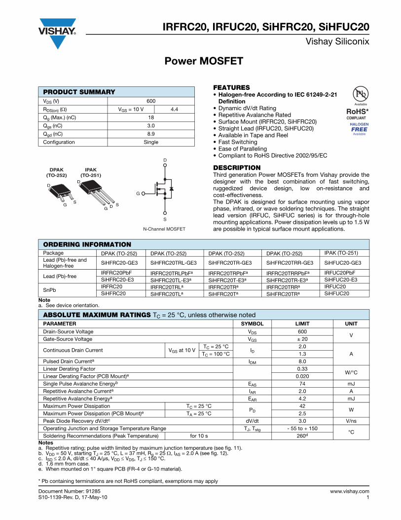
Document Number: 91285 www.vishay.com S10-1139-Rev. D, 17-May-10 1 Power MOSFET IRFRC20, IRFUC20, SiHFRC20, SiHFUC20 Vishay Siliconix FEATURES • Halogen-free According to IEC 61249-2-21 Definition • Dynamic dV/dt Rating • Repetitive Avalanche Rated • Surface Mount (IRFRC20, SiHFRC20) • Straight Lead (IRFUC20, SiHFUC20) • Available in Tape and Reel • Fast Switching • Ease of Paralleling • Compliant to RoHS Directive 2002/95/EC DESCRIPTION Third generation Power MOSFETs from Vishay provide the designer with the best combination of fast switching, ruggedized device design, low on-resistance and cost-effectiveness. The DPAK is designed for surface mounting using vapor phase, infrared, or wave soldering techniques. The straight lead version (IRFUC, SiHFUC series) is for through-hole mounting applications. Power dissipation levels up to 1.5 W are possible in typical surface mount applications. Note a. See device orientation. Notes a. Repetitive rating; pulse width limited by maximum junction temperature (see fig. 11). b. V DD = 50 V, starting T J = 25 °C, L = 37 mH, R g = 25 Ω, I AS = 2.0 A (see fig. 12). c. I SD ≤ 2.0 A, dI/dt ≤ 40 A/μs, V DD ≤ V DS , T J ≤ 150 °C. d. 1.6 mm from case. e. When mounted on 1" square PCB (FR-4 or G-10 material). PRODUCT SUMMARY V DS (V) 600 R DS(on) (Ω) V GS = 10 V 4.4 Q g (Max.) (nC) 18 Q gs (nC) 3.0 Q gd (nC) 8.9 Configuration Single N-Channel MOSFET G D S DPAK (TO-252) IPAK (TO-251) G D S S D G D ORDERING INFORMATION Package DPAK (TO-252) DPAK (TO-252) DPAK (TO-252) DPAK (TO-252) IPAK (TO-251) Lead (Pb)-free and Halogen-free SiHFRC20-GE3 SiHFRC20TRL-GE3 SiHFRC20TR-GE3 SiHFRC20TRR-GE3 SiHFUC20-GE3 Lead (Pb)-free IRFRC20PbF IRFRC20TRLPbF a IRFRC20TRPbF a IRFRC20TRRPbF a IRFUC20PbF SiHFRC20-E3 SiHFRC20TL-E3 a SiHFRC20T-E3 a SiHFRC20TR-E3 a SiHFUC20-E3 SnPb IRFRC20 IRFRC20TRL a IRFRC20TR a IRFRC20TRR a IRFUC20 SiHFRC20 SiHFRC20TL a SiHFRC20T a SiHFRC20TR a SiHFUC20 ABSOLUTE MAXIMUM RATINGS T C = 25 °C, unless otherwise noted PARAMETER SYMBOL LIMIT UNIT Drain-Source Voltage V DS 600 V Gate-Source Voltage V GS ± 20 Continuous Drain Current V GS at 10 V T C = 25 °C I D 2.0 A T C = 100 °C 1.3 Pulsed Drain Current a I DM 8.0 Linear Derating Factor 0.33 W/°C Linear Derating Factor (PCB Mount) e 0.020 Single Pulse Avalanche Energy b E AS 74 mJ Repetitive Avalanche Current a I AR 2.0 A Repetitive Avalanche Energy a E AR 4.2 mJ Maximum Power Dissipation T C = 25 °C P D 42 W Maximum Power Dissipation (PCB Mount) e T A = 25 °C 2.5 Peak Diode Recovery dV/dt c dV/dt 3.0 V/ns Operating Junction and Storage Temperature Range T J , T stg - 55 to + 150 °C Soldering Recommendations (Peak Temperature) for 10 s 260 d * Pb containing terminations are not RoHS compliant, exemptions may apply

Welcome message from author
This document is posted to help you gain knowledge. Please leave a comment to let me know what you think about it! Share it to your friends and learn new things together.
Transcript
Document Number: 91285 www.vishay.comS10-1139-Rev. D, 17-May-10 1
Power MOSFET
IRFRC20, IRFUC20, SiHFRC20, SiHFUC20Vishay Siliconix
FEATURES• Halogen-free According to IEC 61249-2-21
Definition• Dynamic dV/dt Rating• Repetitive Avalanche Rated• Surface Mount (IRFRC20, SiHFRC20)• Straight Lead (IRFUC20, SiHFUC20)• Available in Tape and Reel• Fast Switching• Ease of Paralleling• Compliant to RoHS Directive 2002/95/EC
DESCRIPTIONThird generation Power MOSFETs from Vishay provide thedesigner with the best combination of fast switching,ruggedized device design, low on-resistance andcost-effectiveness.The DPAK is designed for surface mounting using vaporphase, infrared, or wave soldering techniques. The straightlead version (IRFUC, SiHFUC series) is for through-holemounting applications. Power dissipation levels up to 1.5 Ware possible in typical surface mount applications.
Notea. See device orientation.
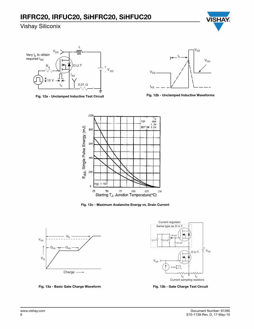
Notesa. Repetitive rating; pulse width limited by maximum junction temperature (see fig. 11).b. VDD = 50 V, starting TJ = 25 °C, L = 37 mH, Rg = 25 Ω, IAS = 2.0 A (see fig. 12).c. ISD ≤ 2.0 A, dI/dt ≤ 40 A/μs, VDD ≤ VDS, TJ ≤ 150 °C.d. 1.6 mm from case.e. When mounted on 1" square PCB (FR-4 or G-10 material).
PRODUCT SUMMARYVDS (V) 600
RDS(on) (Ω) VGS = 10 V 4.4
Qg (Max.) (nC) 18
Qgs (nC) 3.0
Qgd (nC) 8.9
Configuration Single
N-Channel MOSFET
G
D
S
DPAK(TO-252)
IPAK(TO-251)
G D SS
D
G
D
ORDERING INFORMATIONPackage DPAK (TO-252) DPAK (TO-252) DPAK (TO-252) DPAK (TO-252) IPAK (TO-251)Lead (Pb)-free and Halogen-free SiHFRC20-GE3 SiHFRC20TRL-GE3 SiHFRC20TR-GE3 SiHFRC20TRR-GE3 SiHFUC20-GE3
Lead (Pb)-freeIRFRC20PbF IRFRC20TRLPbFa IRFRC20TRPbFa IRFRC20TRRPbFa IRFUC20PbFSiHFRC20-E3 SiHFRC20TL-E3a SiHFRC20T-E3a SiHFRC20TR-E3a SiHFUC20-E3
SnPbIRFRC20 IRFRC20TRLa IRFRC20TRa IRFRC20TRRa IRFUC20SiHFRC20 SiHFRC20TLa SiHFRC20Ta SiHFRC20TRa SiHFUC20
ABSOLUTE MAXIMUM RATINGS TC = 25 °C, unless otherwise notedPARAMETER SYMBOL LIMIT UNIT
Drain-Source Voltage VDS 600V
Gate-Source Voltage VGS ± 20
Continuous Drain Current VGS at 10 VTC = 25 °C
ID2.0
ATC = 100 °C 1.3Pulsed Drain Currenta IDM 8.0Linear Derating Factor 0.33
W/°C Linear Derating Factor (PCB Mount)e 0.020Single Pulse Avalanche Energyb EAS 74 mJ Repetitive Avalanche Currenta IAR 2.0 A Repetitive Avalanche Energya EAR 4.2 mJ Maximum Power Dissipation TC = 25 °C
PD42
W Maximum Power Dissipation (PCB Mount)e TA = 25 °C 2.5Peak Diode Recovery dV/dtc dV/dt 3.0 V/ns Operating Junction and Storage Temperature Range TJ, Tstg - 55 to + 150
°C Soldering Recommendations (Peak Temperature) for 10 s 260d
* Pb containing terminations are not RoHS compliant, exemptions may apply
www.vishay.com Document Number: 912852 S10-1139-Rev. D, 17-May-10
IRFRC20, IRFUC20, SiHFRC20, SiHFUC20Vishay Siliconix
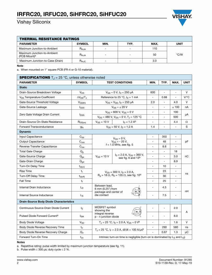
Notea. When mounted on 1" square PCB (FR-4 or G-10 material).
Notesa. Repetitive rating; pulse width limited by maximum junction temperature (see fig. 11).b. Pulse width ≤ 300 μs; duty cycle ≤ 2 %.
THERMAL RESISTANCE RATINGSPARAMETER SYMBOL MIN. TYP. MAX. UNIT
Maximum Junction-to-Ambient RthJA - - 110
°C/WMaximum Junction-to-Ambient (PCB Mount)a RthJA - - 50
Maximum Junction-to-Case (Drain) RthJC - - 3.0
SPECIFICATIONS TJ = 25 °C, unless otherwise notedPARAMETER SYMBOL TEST CONDITIONS MIN. TYP. MAX. UNIT
Static
Drain-Source Breakdown Voltage VDS VGS = 0 V, ID = 250 μA 600 - - V
VDS Temperature Coefficient ΔVDS/TJ Reference to 25 °C, ID = 1 mA - 0.88 - V/°C
Gate-Source Threshold Voltage VGS(th) VDS = VGS, ID = 250 μA 2.0 - 4.0 V
Gate-Source Leakage IGSS VGS = ± 20 V - - ± 100 nA
Zero Gate Voltage Drain Current IDSS VDS = 600 V, VGS = 0 V - - 100
μA VDS = 480 V, VGS = 0 V, TJ = 125 °C - - 500
Drain-Source On-State Resistance RDS(on) VGS = 10 V ID = 1.2 Ab - - 4.4 Ω
Forward Transconductance gfs VDS = 50 V, ID = 1.2 A 1.4 - - S
Dynamic
Input Capacitance Ciss VGS = 0 V, VDS = - 25 V,
f = 1.0 MHz, see fig. 5
- 350 -
pFOutput Capacitance Coss - 48 -
Reverse Transfer Capacitance Crss - 8.6 -
Total Gate Charge Qg
VGS = 10 V ID = 2.0 A, VDS = 360 V, see fig. 6 and 13b
- - 18
nC Gate-Source Charge Qgs - - 3.0
Gate-Drain Charge Qgd - - 8.9
Turn-On Delay Time td(on)
VDD = 300 V, ID = 2.0 A, Rg = 18 Ω, RD = 135 Ω, see fig. 10b
- 10 -
nsRise Time tr - 23 -
Turn-Off Delay Time td(off) - 30 -
Fall Time tf - 25 -
Internal Drain Inductance LD Between lead,6 mm (0.25") from package and center of die contact
- 4.5 -nH
Internal Source Inductance LS - 7.5 -
Drain-Source Body Diode Characteristics
Continuous Source-Drain Diode Current IS MOSFET symbolshowing the integral reversep - n junction diode
- - 2.0A
Pulsed Diode Forward Currenta ISM - - 8.0
Body Diode Voltage VSD TJ = 25 °C, IS = 2.0 A, VGS = 0 Vb - - 1.6 V
Body Diode Reverse Recovery Time trrTJ = 25 °C, IF = 2.0 A, dI/dt = 100 A/μsb
- 290 580 ns
Body Diode Reverse Recovery Charge Qrr - 0.67 1.3 μC
Forward Turn-On Time ton Intrinsic turn-on time is negligible (turn-on is dominated by LS and LD)
D
S
G
S
D
G
Document Number: 91285 www.vishay.comS10-1139-Rev. D, 17-May-10 3
IRFRC20, IRFUC20, SiHFRC20, SiHFUC20Vishay Siliconix
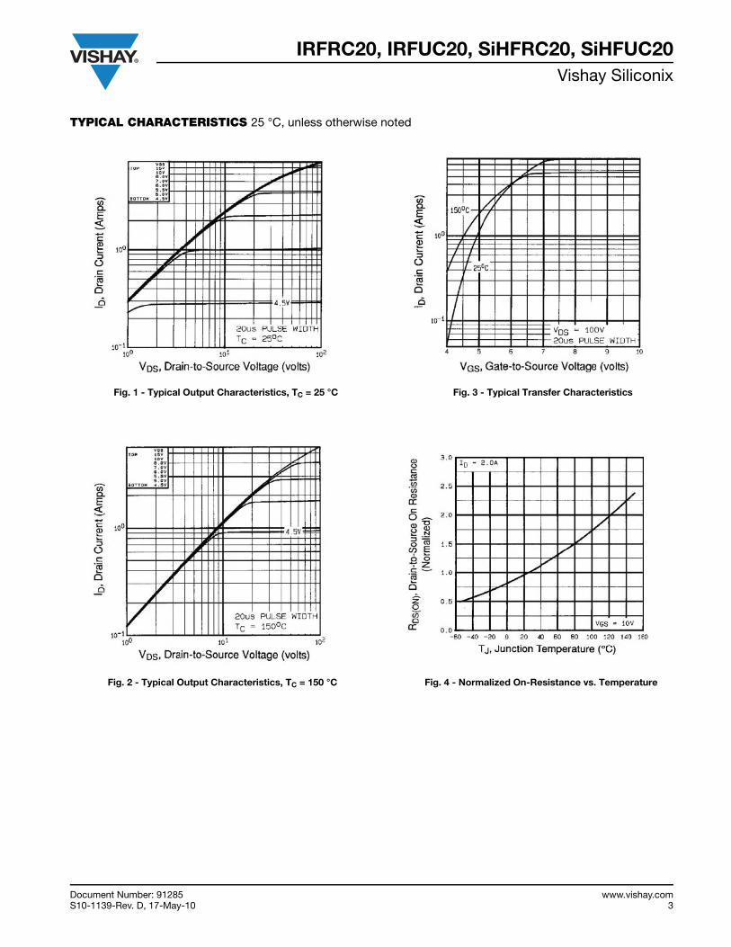
TYPICAL CHARACTERISTICS 25 °C, unless otherwise noted
Fig. 1 - Typical Output Characteristics, TC = 25 °C
Fig. 2 - Typical Output Characteristics, TC = 150 °C
Fig. 3 - Typical Transfer Characteristics
Fig. 4 - Normalized On-Resistance vs. Temperature
www.vishay.com Document Number: 912854 S10-1139-Rev. D, 17-May-10
IRFRC20, IRFUC20, SiHFRC20, SiHFUC20Vishay Siliconix
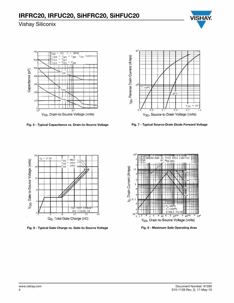
Fig. 5 - Typical Capacitance vs. Drain-to-Source Voltage
Fig. 6 - Typical Gate Charge vs. Gate-to-Source Voltage
Fig. 7 - Typical Source-Drain Diode Forward Voltage
Fig. 8 - Maximum Safe Operating Area
Document Number: 91285 www.vishay.comS10-1139-Rev. D, 17-May-10 5
IRFRC20, IRFUC20, SiHFRC20, SiHFUC20Vishay Siliconix
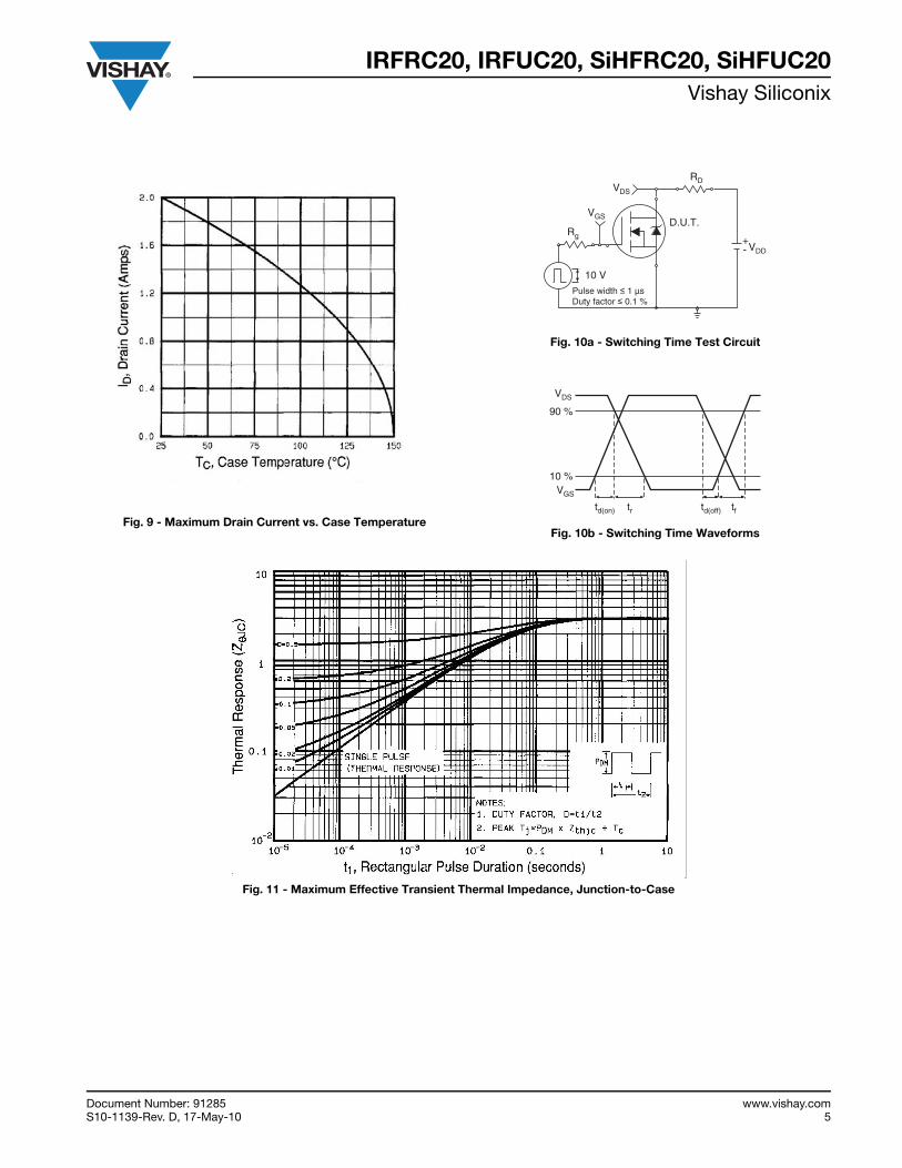
Fig. 9 - Maximum Drain Current vs. Case Temperature
Fig. 10a - Switching Time Test Circuit
Fig. 10b - Switching Time Waveforms
Fig. 11 - Maximum Effective Transient Thermal Impedance, Junction-to-Case
Pulse width ≤ 1 µsDuty factor ≤ 0.1 %
RD
VGS
Rg
D.U.T.
10 V
+-
VDS
VDD
VDS
90 %
10 %VGS
td(on) tr td(off) tf
www.vishay.com Document Number: 912856 S10-1139-Rev. D, 17-May-10
IRFRC20, IRFUC20, SiHFRC20, SiHFUC20Vishay Siliconix
Fig. 12a - Unclamped Inductive Test Circuit Fig. 12b - Unclamped Inductive Waveforms
Fig. 12c - Maximum Avalanche Energy vs. Drain Current
Fig. 13a - Basic Gate Charge Waveform Fig. 13b - Gate Charge Test Circuit
Rg
IAS
0.01 Ωtp
D.U.T
LVDS
+
-VDD
10 V
Vary tp to obtainrequired IAS
IAS
VDS
VDD
VDS
tp
QGS QGD
QG
VG
Charge
VGS
D.U.T.
3 mA
VGS
VDS
IG ID
0.3 µF0.2 µF
50 kΩ
12 V
Current regulator
Current sampling resistors
Same type as D.U.T.
+
-
Document Number: 91285 www.vishay.comS10-1139-Rev. D, 17-May-10 7
IRFRC20, IRFUC20, SiHFRC20, SiHFUC20Vishay Siliconix
Fig. 14 - For N-Channel
Vishay Siliconix maintains worldwide manufacturing capability. Products may be manufactured at one of several qualified locations. Reliability data for Silicon
Technology and Package Reliability represent a composite of all qualified locations. For related documents such as package/tape drawings, part marking, and
reliability data, see www.vishay.com/ppg?91285.
P.W.Period
dI/dt
Diode recoverydV/dt
Ripple ≤ 5 %
Body diode forward drop
Re-appliedvoltage
Reverserecoverycurrent
Body diode forwardcurrent
VGS = 10 Va
ISD
Driver gate drive
D.U.T. lSD waveform
D.U.T. VDS waveform
Inductor current
D = P.W.Period
+
-
+
+
+-
-
-
Peak Diode Recovery dV/dt Test Circuit
VDD
• dV/dt controlled by Rg
• Driver same type as D.U.T.• ISD controlled by duty factor “D”• D.U.T. - device under test
D.U.T.Circuit layout considerations
• Low stray inductance• Ground plane• Low leakage inductance
current transformer
Rg
Notea. VGS = 5 V for logic level devices
VDD
Document Number: 91344 www.vishay.comRevision: 15-Sep-08 1
Package InformationVishay Siliconix
TO-252AA (HIGH VOLTAGE)
Notes1. Package body sizes exclude mold flash, protrusion or gate burrs. Mold flash, protrusion or gate burrs shall not exceed 0.10 mm per side.2. Package body sizes determined at the outermost extremes of the plastic body exclusive of mold flash, gate burrs and interlead flash, but
including any mismatch between the top and bottom of the plastic body.3. The package top may be smaller than the package bottom.4. Dimension "b" does not include dambar protrusion. Allowable dambar protrusion shall be 0.10 mm total in excess of "b" dimension at maximum
material condition. The dambar cannot be located on the lower radius of the foot.
E
b3
L3
L4
b2
e
b
D H
E1
D1
A
c2
L1
L2
c
A1
Lθ
MILLIMETERS INCHES
DIM. MIN. MAX. MIN. MAX.
E 6.40 6.73 0.252 0.265
L 1.40 1.77 0.055 0.070
L1 2.743 REF 0.108 REF
L2 0.508 BSC 0.020 BSC
L3 0.89 1.27 0.035 0.050
L4 0.64 1.01 0.025 0.040
D 6.00 6.22 0.236 0.245
H 9.40 10.40 0.370 0.409
b 0.64 0.88 0.025 0.035
b2 0.77 1.14 0.030 0.045
b3 5.21 5.46 0.205 0.215
e 2.286 BSC 0.090 BSC
A 2.20 2.38 0.087 0.094
A1 0.00 0.13 0.000 0.005
c 0.45 0.60 0.018 0.024
c2 0.45 0.58 0.018 0.023
D1 5.30 - 0.209 -
E1 4.40 - 0.173 -
θ 0' 10' 0' 10'
ECN: S-81965-Rev. A, 15-Sep-08DWG: 5973
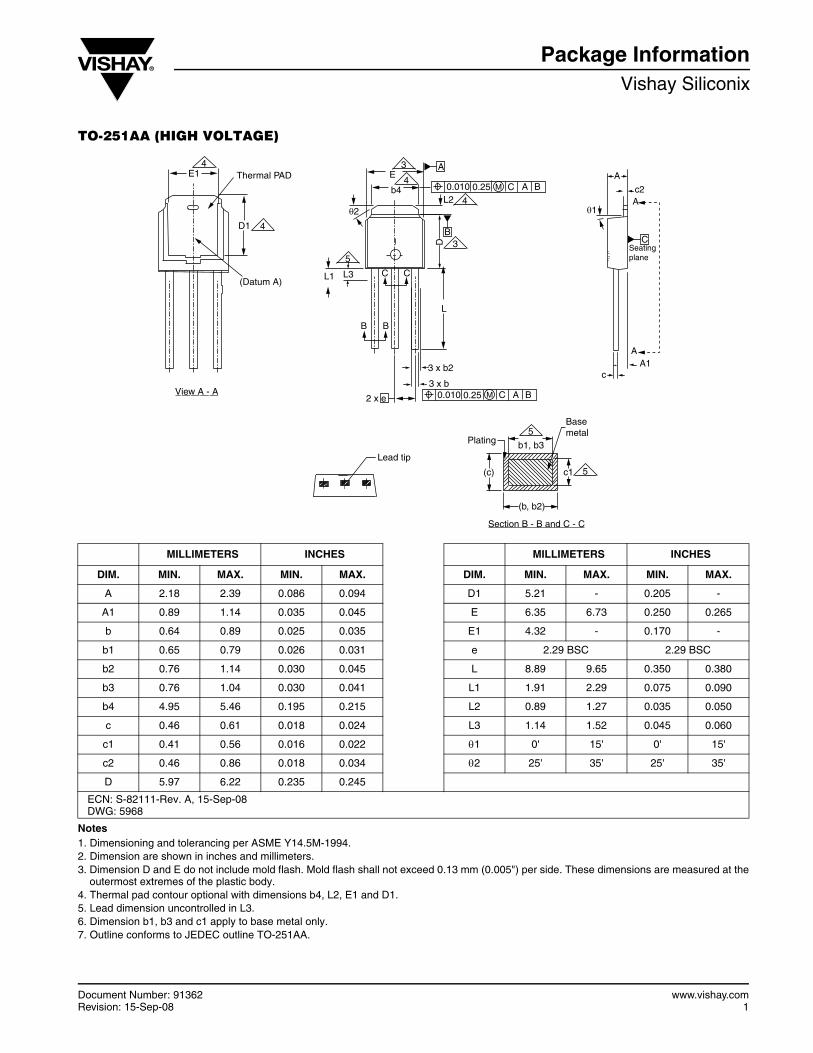
Document Number: 91362 www.vishay.comRevision: 15-Sep-08 1
Package InformationVishay Siliconix
TO-251AA (HIGH VOLTAGE)
Notes1. Dimensioning and tolerancing per ASME Y14.5M-1994.2. Dimension are shown in inches and millimeters.3. Dimension D and E do not include mold flash. Mold flash shall not exceed 0.13 mm (0.005") per side. These dimensions are measured at the
outermost extremes of the plastic body.4. Thermal pad contour optional with dimensions b4, L2, E1 and D1.5. Lead dimension uncontrolled in L3.6. Dimension b1, b3 and c1 apply to base metal only.7. Outline conforms to JEDEC outline TO-251AA.
Basemetal
Plating b1, b3
(b, b2)
c1(c)
Section B - B and C - C
D
A
c2
c
Lead tip
5
5
(Datum A)
Thermal PADE1
4D1
View A - A
A1A
A
CSeatingplane
C C
B B
θ1θ2
B
4
4
4
3
5
L1
L
L3
3 x b2
3 x b
3
b4
E
2 x e 0.010 C BM A0.25
0.010 BA0.25L2
A
CM
MILLIMETERS INCHES MILLIMETERS INCHES
DIM. MIN. MAX. MIN. MAX. DIM. MIN. MAX. MIN. MAX.
A 2.18 2.39 0.086 0.094 D1 5.21 - 0.205 -
A1 0.89 1.14 0.035 0.045 E 6.35 6.73 0.250 0.265
b 0.64 0.89 0.025 0.035 E1 4.32 - 0.170 -
b1 0.65 0.79 0.026 0.031 e 2.29 BSC 2.29 BSC
b2 0.76 1.14 0.030 0.045 L 8.89 9.65 0.350 0.380
b3 0.76 1.04 0.030 0.041 L1 1.91 2.29 0.075 0.090
b4 4.95 5.46 0.195 0.215 L2 0.89 1.27 0.035 0.050
c 0.46 0.61 0.018 0.024 L3 1.14 1.52 0.045 0.060
c1 0.41 0.56 0.016 0.022 θ1 0' 15' 0' 15'
c2 0.46 0.86 0.018 0.034 θ2 25' 35' 25' 35'
D 5.97 6.22 0.235 0.245
ECN: S-82111-Rev. A, 15-Sep-08DWG: 5968
Legal Disclaimer Noticewww.vishay.com Vishay
Revision: 12-Mar-12 1 Document Number: 91000
DisclaimerALL PRODUCT, PRODUCT SPECIFICATIONS AND DATA ARE SUBJECT TO CHANGE WITHOUT NOTICE TO IMPROVERELIABILITY, FUNCTION OR DESIGN OR OTHERWISE.
Vishay Intertechnology, Inc., its affiliates, agents, and employees, and all persons acting on its or their behalf (collectively,“Vishay”), disclaim any and all liability for any errors, inaccuracies or incompleteness contained in any datasheet or in any otherdisclosure relating to any product.
Vishay makes no warranty, representation or guarantee regarding the suitability of the products for any particular purpose orthe continuing production of any product. To the maximum extent permitted by applicable law, Vishay disclaims (i) any and allliability arising out of the application or use of any product, (ii) any and all liability, including without limitation special,consequential or incidental damages, and (iii) any and all implied warranties, including warranties of fitness for particularpurpose, non-infringement and merchantability.
Statements regarding the suitability of products for certain types of applications are based on Vishay’s knowledge of typicalrequirements that are often placed on Vishay products in generic applications. Such statements are not binding statementsabout the suitability of products for a particular application. It is the customer’s responsibility to validate that a particularproduct with the properties described in the product specification is suitable for use in a particular application. Parametersprovided in datasheets and/or specifications may vary in different applications and performance may vary over time. Alloperating parameters, including typical parameters, must be validated for each customer application by the customer’stechnical experts. Product specifications do not expand or otherwise modify Vishay’s terms and conditions of purchase,including but not limited to the warranty expressed therein.
Except as expressly indicated in writing, Vishay products are not designed for use in medical, life-saving, or life-sustainingapplications or for any other application in which the failure of the Vishay product could result in personal injury or death.Customers using or selling Vishay products not expressly indicated for use in such applications do so at their own risk and agreeto fully indemnify and hold Vishay and its distributors harmless from and against any and all claims, liabilities, expenses anddamages arising or resulting in connection with such use or sale, including attorneys fees, even if such claim alleges that Vishayor its distributor was negligent regarding the design or manufacture of the part. Please contact authorized Vishay personnel toobtain written terms and conditions regarding products designed for such applications.
No license, express or implied, by estoppel or otherwise, to any intellectual property rights is granted by this document or byany conduct of Vishay. Product names and markings noted herein may be trademarks of their respective owners.
Material Category PolicyVishay Intertechnology, Inc. hereby certifies that all its products that are identified as RoHS-Compliant fulfill thedefinitions and restrictions defined under Directive 2011/65/EU of The European Parliament and of the Councilof June 8, 2011 on the restriction of the use of certain hazardous substances in electrical and electronic equipment(EEE) - recast, unless otherwise specified as non-compliant.
Please note that some Vishay documentation may still make reference to RoHS Directive 2002/95/EC. We confirm thatall the products identified as being compliant to Directive 2002/95/EC conform to Directive 2011/65/EU.
Related Documents